JP4337222B2 - Projection display - Google Patents
Projection displayDownload PDFInfo
- Publication number
- JP4337222B2 JP4337222B2JP2000074366AJP2000074366AJP4337222B2JP 4337222 B2JP4337222 B2JP 4337222B2JP 2000074366 AJP2000074366 AJP 2000074366AJP 2000074366 AJP2000074366 AJP 2000074366AJP 4337222 B2JP4337222 B2JP 4337222B2
- Authority
- JP
- Japan
- Prior art keywords
- liquid crystal
- light
- crystal panel
- optical shutter
- level
- Prior art date
- Legal status (The legal status is an assumption and is not a legal conclusion. Google has not performed a legal analysis and makes no representation as to the accuracy of the status listed.)
- Expired - Fee Related
Links
- 239000004973liquid crystal related substanceSubstances0.000claimsdescription261
- 230000003287optical effectEffects0.000claimsdescription174
- 238000005286illuminationMethods0.000claimsdescription33
- 210000001747pupilAnatomy0.000claimsdescription32
- 239000004983Polymer Dispersed Liquid CrystalSubstances0.000claimsdescription13
- 230000003247decreasing effectEffects0.000claimsdescription9
- 230000000903blocking effectEffects0.000claimsdescription6
- 239000004988Nematic liquid crystalSubstances0.000claimsdescription3
- 238000002834transmittanceMethods0.000description30
- 238000003491arrayMethods0.000description15
- 230000008859changeEffects0.000description15
- 230000007423decreaseEffects0.000description14
- 238000010586diagramMethods0.000description14
- 230000000694effectsEffects0.000description12
- 230000009467reductionEffects0.000description6
- 230000005540biological transmissionEffects0.000description5
- 238000006243chemical reactionMethods0.000description5
- 238000001514detection methodMethods0.000description5
- 238000003384imaging methodMethods0.000description5
- 230000010287polarizationEffects0.000description4
- 230000008901benefitEffects0.000description2
- 230000004907fluxEffects0.000description2
- 230000004048modificationEffects0.000description2
- 238000012986modificationMethods0.000description2
- 238000010438heat treatmentMethods0.000description1
- 238000004519manufacturing processMethods0.000description1
- 239000000463materialSubstances0.000description1
- 239000011159matrix materialSubstances0.000description1
- QSHDDOUJBYECFT-UHFFFAOYSA-NmercuryChemical compound[Hg]QSHDDOUJBYECFT-UHFFFAOYSA-N0.000description1
- 229910052753mercuryInorganic materials0.000description1
- 229910001507metal halideInorganic materials0.000description1
- 150000005309metal halidesChemical class0.000description1
- 230000002093peripheral effectEffects0.000description1
- 230000004044responseEffects0.000description1
- 239000000758substrateSubstances0.000description1
- 229910052724xenonInorganic materials0.000description1
- FHNFHKCVQCLJFQ-UHFFFAOYSA-Nxenon atomChemical compound[Xe]FHNFHKCVQCLJFQ-UHFFFAOYSA-N0.000description1
Images


Classifications
- H—ELECTRICITY
- H04—ELECTRIC COMMUNICATION TECHNIQUE
- H04N—PICTORIAL COMMUNICATION, e.g. TELEVISION
- H04N9/00—Details of colour television systems
- H04N9/12—Picture reproducers
- H04N9/31—Projection devices for colour picture display, e.g. using electronic spatial light modulators [ESLM]
- H04N9/3102—Projection devices for colour picture display, e.g. using electronic spatial light modulators [ESLM] using two-dimensional electronic spatial light modulators
- H04N9/312—Driving therefor
- H04N9/3126—Driving therefor for spatial light modulators in series
Landscapes
- Liquid Crystal (AREA)
- Engineering & Computer Science (AREA)
- Multimedia (AREA)
- Signal Processing (AREA)
- Projection Apparatus (AREA)
- Liquid Crystal Display Device Control (AREA)
- Transforming Electric Information Into Light Information (AREA)
- Control Of Indicators Other Than Cathode Ray Tubes (AREA)
Description
Translated fromJapanese【0001】
【発明の属する技術分野】
本発明は、液晶パネルを空間光変調素子として用いた投射型表示装置に関する。
【0002】
【従来の技術】
画像をスクリーンに拡大投影することにより大画面を実現する投射型表示装置が、屋内外用の大画面の画像表示装置として普及している。この投射型表示装置は、CRTの蛍光面からの出射光をスクリーンに投射するもの(CRTプロジェクタ装置)と、光源からの出射光を空間光変調素子で変調してスクリーンに投射するものとに大別されるが、後者では、液晶パネルを空間光変調素子として用いるもの(液晶プロジェクタ装置)が主流になっている。
【0003】
図13は、従来の液晶プロジェクタ装置の光学系の構成例を示す。光源51から出射した光(非偏光)が、光源からの出射光を液晶パネルに導く光学系である照明光学系(図ではそのうちの集光レンズ52のみを示している)を経て、TN(ツイストネマティック)液晶を用いた透過型の液晶パネル53に入射する。液晶パネル53では、この入射光のうちの一方の振動方向の直線偏光のみが、表面の偏光板(偏光子)を経て液晶層を通過する。この直線偏光は、映像信号のレベルに応じて液晶パネル53に印加される駆動電圧によって変調され(振動方向が最大90゜回転し)、液晶パネル53の反対側の表面の偏光板(検光子)で検光される。こうして液晶パネル53を透過した光が、液晶パネルからの出射光をスクリーンに導く光学系である投射光学系(図ではそのうちの投射レンズ54のみを示している)を経てスクリーン(図示略)に投射される。
【0004】
【発明が解決しようとする課題】
液晶プロジェクタ装置には、CRTプロジェクタ装置と比較して、小型・軽量な装置で大画面を実現できるという利点や、光源や照明光学系を液晶パネルとは独立して設けるのでそれらの改良による高輝度化が容易であるという利点がある。
【0005】
しかし、その反面、従来の液晶プロジェクタ装置には、低輝度部分での階調表現が劣るという欠点や、黒色の浮きが発生するのでコントラストが低いという欠点があった。
【0006】
低輝度の部分での階調表現が劣る原因は、液晶パネルの印加電圧−透過率特性にある。液晶パネルの印加電圧−透過率特性は、図14に例示するように、透過率が高い(図では90%以上の)範囲(すなわち高輝度部分)では、印加電圧の変化に対する透過率の変化が緩やかであるのに対し、透過率が低い(図では10%から90%の)範囲(すなわち低輝度部分)では、印加電圧の変化に対する透過率の変化が急峻になっている。(図14の横軸上において印加電圧が増大する向きは、液晶パネルの種類によって、左向きと右向きとの両方があり得る)。
【0007】
しかも、この印加電圧−透過率特性は、液晶層の厚さ(すなわち液晶パネルのセルギャップの大きさ)と高い相関を持つので、個々の液晶パネル毎に(したがって個々の液晶プロジェクタ装置毎に)多少ばらつきがあるとともに、1つの液晶パネルでも部位によって多少ばらつきがある。そのため、低輝度部分では、印加電圧を制御することにより輝度を細かく調整することが困難である(すなわち階調表現が劣る)。
【0008】
なお、この低輝度部分での階調表現が劣るという欠点は、もともと輝度の低い画像を表示する場合だけでなく、液晶プロジェクタ装置の輝度調整用釦を操作して輝度を下げる場合にも現れていた。すなわち、従来の液晶プロジェクタ装置では、輝度調整用釦で輝度を下げる操作が行われた場合、液晶パネルの透過率が低くなるように印加電圧を変化させていたので、図14のような印加電圧−透過率特性から、やはり階調表現が劣ってしまう。
【0009】
次に、黒色の浮きが発生する原因は、液晶パネルの電極基板上の配向膜にもたせたプレチルト角(配向膜と液晶分子とのなす角度)にある。液晶パネルでは、入射した直線偏光の振動方向を液晶層内で回転させない(または90゜回転させる)ときにも、このプレチルト角の存在により、入射した直線偏光が楕円偏光になってしまうことがある。低輝度部分でこの現象が起きると、楕円偏光が部分的に検光子を通過して投射レンズに入射してしまうので、黒色の浮きが発生してコントラストが低下する。
【0010】
そして、液晶プロジェクタ装置では、より明るい画像を表示することを目的として、照明光学系のFナンバを小さくすることにより光源からの光の液晶パネルへの入射角を大きくする傾向にあるが、この入射角が大きくなるにつれて、プレチルトを原因とするコントラストの低下の度合いは顕著になることが知られている。図15は、このコントラストの低下の度合いと液晶パネルへの入射角との関係(「コントラスト視野角特性」と呼ぶことにする)を例示したものである。液晶パネルのパネル面に平行な方向での光の入射方向φにかかわらず、入射角θが大きくなるほどコントラストCRが低くなっている。ただし、同一の入射角θの値に対するコントラストCRの値は入射方向φによって異なっており、全ての入射方向φに亘ってコントラストCRの値が等しい入射角θの値を結んだ線(「等コントラスト線」と呼ぶことにする)は、縦横比が概ね1:2程度の楕円形や長方形に近似した形状をしている。
【0011】
このように、従来の液晶プロジェクタ装置には、低輝度部分での階調表現が劣るという欠点や、コントラストが低いという欠点があった。これに対し、こうした欠点を解消する試みも従来から全くなされていないわけではない。例えば特開平6−102484号公報には、光出力レベルの可変な光源を設け、所定期間毎に、映像信号のピークレベルが所定の基準レベルよりも低い場合に、この光源の出力レベルを小さくするとともに、映像信号のレベルを大きくして液晶パネルを駆動するようにした液晶プロジェクタ装置が開示されている。
【0012】
この液晶プロジェクタ装置では、映像信号のピークレベルが基準レベルよりも低い場合には(すなわち低輝度部分では)、光源の出力レベルを小さくするのでスクリーンへの投射光量が減少するとともに、映像信号のレベルを大きくして液晶パネルを駆動するので液晶パネルの透過率が高くなる。したがって、低輝度部分でも、図14の印加電圧−透過率特性特性のうち印加電圧の変化に対する透過率の変化が緩やかである範囲を利用して、輝度を細かく調整することができるようになる(すなわち階調表現が改善される)。
【0013】
しかし、この液晶プロジェクタ装置では、スクリーンへの投射光量の減少を、出力レベルの可変な光源を設けることによって実現している。一般に液晶プロジェクタ装置では、光源として、高い発光効率を有する放電ランプ(超高圧水銀ランプ,メタルハライドランプまたはキセノンランプ等)が用いられることが多いが、こうした放電ランプの光出力レベルを可変にした場合には、放電ランプの電源部の構成が複雑になってしまう。
【0014】
また、この液晶プロジェクタ装置では、もともと輝度の低い画像を表示する場合ではなく液晶プロジェクタ装置の輝度調整用釦を操作して輝度を下げる場合には、階調表現が改善されない。
【0015】
また、この液晶プロジェクタ装置では、光源の出力レベルを小さくした際に、図16に示すように、液晶パネルへの入射角が小さい光の液晶パネルへの入射光量も、この入射角が大きい光の液晶パネルへの入射光量も、均等に減少する。そのため、光源の出力レベルを小さくしても、液晶パネルへの入射角が大きい光(すなわち、図15に示したようなコントラスト視野角特性から、コントラストを低下させる度合いの大きい光)が依然としてある程度液晶パネルに入射するので、黒色の浮きの発生によるコントラストの低下は抑制されない。
【0016】
本発明は、上述の点に鑑み、液晶プロジェクタ装置において、光源の構成の複雑化を招くことなく、低輝度部分の階調表現を改善することや、黒色の浮きの発生によるコントラストの低下を抑制することを課題としてなされたものである。
【0017】
【課題を解決するための手段】
この課題を解決するために、本出願人は、入射光を変調して出射する液晶パネルと、光源からの出射光をこの液晶パネルに入射させる照明光学系と、この液晶パネルからの出射光をスクリーンに導く投射光学系とを有する投射型表示装置(すなわち液晶プロジェクタ装置)において、この液晶パネルへの入射角の大きい光の順に遮断する光シャッタを、照明光学系と投射光学系とのいずれか一方に配置し、所定期間毎に、外部から供給される映像信号のピークレベルを検出し、そのピークレベルが所定の基準レベルよりも小さい場合に、この光シャッタで光を遮断させるとともに、この映像信号のレベルを増大させてこの液晶パネルを駆動させる制御手段を備えたものを提案する。
【0018】
この液晶プロジェクタ装置では、液晶パネルへの入射角の大きい光の順に遮断する光シャッタが、照明光学系と投射光学系とのいずれか一方に配置される。そして、制御手段により、所定期間毎に、外部から供給される映像信号のピークレベルが検出され、そのピークレベルが所定の基準レベルよりも小さい場合に、この光シャッタで光が遮断されるとともに、この映像信号のレベルが増大されて液晶パネルが駆動されることにより液晶パネルの透過率が高くなる。
【0019】
このように、外部から供給される映像信号のピークレベルが基準レベルよりも低い期間では(すなわち低輝度部分では)、光シャッタで光が遮断されることによりスクリーンへの投射光量が減少するとともに、液晶パネルの透過率が高くなる。
【0020】
したがって、低輝度部分でも、出力レベルの可変な光源を設けることによる光源の構成の複雑化を招くことなく、図14のような印加電圧−透過率特性特性のうち印加電圧の変化に対する透過率の変化が緩やかである範囲(透過率が高い範囲)を利用して、輝度を細かく調整することができる(すなわち階調表現が改善される)。
【0021】
そして、この液晶プロジェクタ装置では、光シャッタが液晶パネルへの入射角の大きい光の順に遮断するので、低輝度部分では、図15のようなコントラスト視野角特性から、コントラストを低下させる度合いの大きい光のほうが、コントラストを低下させる度合いの小さい光よりも多く遮断されるようになる。これにより、コントラストを低下させる度合いの大きい光のスクリーンへの投射量が、コントラストを低下させる度合いの小さい光のスクリーンへの投射量よりも多く減少するので、黒色の浮きの発生によるコントラストの低下が抑制される。
【0022】
なお、一例として、この光シャッタを、液晶パネルのコントラスト視野角特性に基づき、液晶パネルへの入射角が大きく、コントラストを低下させる度合いの大きい光の順に遮断するように構成することが好適である。それにより、液晶パネルへの入射角が大きくコントラストを低下させる度合いの大きい光の順に光シャッタで遮断されてスクリーンに投射されなくなるので、黒色の浮きの発生によるコントラストの低下が一層よく抑制されるようになる。
【0023】
また、一例として、この光シャッタを、照明光学系の略瞳位置と投射光学系の略瞳位置とのいずれか一方に配置することが好適である。
【0024】
ここで、光学系の瞳位置を通過する光束の断面形状と、結像位置でのその光の角度分布とには、光学系の瞳位置において任意の断面形状で光束を通過させると、結像位置でのその光の角度分布がその断面形状と相似形になるという関係がある。したがって、照明光学系の略瞳位置にこの光シャッタを配置した場合には、液晶パネルに入射(結像)する光の角度分布が、光シャッタを通過する光の断面形状と略相似形になり、その角度分布を越える入射角では液晶パネルに光が入射しなくなる。また、投射光学系の略瞳位置にこの光シャッタを配置した場合にも、液晶パネルに入射した光のうち、光シャッタを通過する光の断面形状と略相似形の角度分布を越える入射角の光は、液晶パネルから出射しても光シャッタを通過しなくなる(したがってスクリーンに投射されなくなる)。
【0025】
したがって、いずれの場合にも、例えば円形の断面形状の光を通過させるように光シャッタを構成することにより、液晶パネルへの入射角の大きい光の順に遮断することが容易になり、また例えば液晶パネルの等コントラスト線(図15参照)に略等しい断面形状の光を通過させるように光シャッタを構成することにより、コントラストを低下させる度合いの大きい光の順に遮断することが容易になる。
【0026】
また、一例として、この制御手段を、ピークレベルが基準レベルよりも小さい場合に、ピークレベル,基準レベルをそれぞれVp,Vmaxとして、(1−Vp/Vmax)の値に応じた量の光を光シャッタで遮断させるとともに、外部から供給される映像信号のレベルをVmax/Vp倍に増大させて液晶パネルを駆動させるように構成することが好適である。
【0027】
液晶パネルから投射レンズを経てスクリーンに投影される画像の明るさは、この光シャッタでの光の通過率と、液晶パネルを駆動する映像信号のレベルの増大率との積によって決定される。したがって、このように(1−Vp/Vmax)の値に応じた量の光を光シャッタで遮断させる(すなわちVp/Vmaxの値に応じた量の光を光シャッタで通過させる)とともに、液晶パネルを駆動する映像信号のレベルをVmax/Vp倍に増大させることにより、スクリーンに投影される画像の明るさが、この光シャッタで光を遮断しないとともにもとの映像信号のレベルのままで液晶パネルを駆動する場合の明るさからずれることが抑制される。(光シャッタでちょうど(1−Vp/Vmax)の量の光を遮断させた場合には、光シャッタの通過率(Vp/Vmax)×レベルの増大率(Vmax/Vp)=1となるので、スクリーンに投影される画像の明るさを、この光シャッタで光を全く遮断しないとともにもとの映像信号のレベルのままで液晶パネルを駆動する場合と同じにすることができる。)
【0028】
また、この光シャッタを、例えばツイストネマティック液晶を用いた液晶パネルで光を遮断するように構成するか、あるいは別の例として高分子分散液晶を用いた液晶パネルで光を遮断するように構成することが好適である。
【0029】
こうした液晶パネルで光シャッタで光を遮断することにより、機械的に動作する部品で光を遮断するよりも、光シャッタの高速動作が可能になる。したがって、映像信号のレベルの変化にすばやく応答して、光を遮断するか否か、どの程度の量の光を遮断するかを切り換えることができるようになる。
【0030】
また、こうした液晶パネルで光シャッタを構成する場合には、一例として、複数の同心の固定パターン電極を有する液晶パネルを用いることが好適である。それにより、液晶パネルで光シャッタを構成する場合の光シャッタの構造や制御が簡単になる。
【0049】
【発明の実施の形態】
以下、本発明の実施の形態を図を用いて説明する。
図1は、本発明に係る液晶プロジェクタ装置の構成例を示す。この液晶プロジェクタ装置の光学系は、光源1と、照明光学系2と、空間光変調素子としての透過型の液晶パネル3と、投射光学系(図にはそのうちの投射レンズ4のみを示している)とに大別される。
【0050】
光源1は、放電ランプ5と、放電ランプ5の光(非偏光)を一定方向に指向させる反射鏡6とで構成されている。
【0051】
照明光学系2には、最も光源1寄りの位置に、光源1からの出射光のうちP偏光を通過させS偏光を反射するPBS(偏光ビームスプリッタ)7と、PBS7で反射されたS偏光をPBS7からのP偏光の出射方向と同じ方向に反射する反射鏡8と、反射鏡8で反射されたS偏光が入射する1/2波長板9とが設けられている。
【0052】
光源1からの出射光のうちのP偏光は、PBS7をそのまま通過する。他方、光源1からの出射光のうちのS偏光は、PBS7で反射され、反射鏡8でPBS7からのP偏光の出射方向と同じ方向に反射された後、1/2波長板9でP偏光にされる。これにより、光源1から出射した非偏光は、P偏光に変換されて、PBS7及び1/2波長板9から同じ方向に出射する。
【0053】
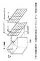
PBS7に対する反射鏡8及び1/2波長板9の配置は、図2に示すように、PBS7から出射したP偏光と1/2波長板9から出射したP偏光とを合わせた光束の断面形状が、液晶パネル3の等コントラスト線(図15に示したような楕円形や長方形に近似した形状)の縦横比と略等しい縦横比(約1:2とする)の楕円形になるように決定されている。
【0054】
図1に示すように、照明光学系2のうちPBS7,反射鏡8及び1/2波長板9よりも液晶パネル3寄りの位置には、マイクロレンズアレイ10,マイクロレンズアレイ11,光シャッタ12,集光レンズ13が順に設けられている。PBS7から出射したP偏光と1/2波長板9から出射したP偏光とは、マイクロレンズアレイ10に入射する。
【0055】
マイクロレンズアレイ10,11は、それぞれ小さな(例えば直径1〜5mm程度の)レンズ10a,11aを複数個アレイ状に配列したものである(図では便宜上個々のレンズ10a,11aを実際よりも大きく描いている)。
【0056】
図2に示すように、全てのレンズ10a,11aを合わせた形状は、それぞれ縦横比約1:2(液晶パネル3の等コントラスト線と略等しい縦横比)の長方形になっている。マイクロレンズアレイ10,11は、この長方形の長辺の方向を、PBS7から出射したP偏光と1/2波長板9から出射したP偏光とを合わせた光束の断面である略楕円形の長辺の方向と一致させてそれぞれ配置されている。
【0057】
マイクロレンズアレイ10のレンズ10aの形状は、レンズ10aからの光が液晶パネル3のパネル面上に集光されるようにするために、液晶パネル3のパネル面と相似形の長方形になっている。
【0058】
マイクロレンズアレイ11は、マイクロレンズアレイ10のレンズ10aの略焦点位置に配置されている。マイクロレンズアレイ11のレンズ11aの形状は、レンズ10aと一対一に対応して、対応するレンズ10aからの光をできるだけ多く入射できる形状になっている(図2では長方形になっているが、例えば円形であってもよい)。
【0059】
ここで、この照明光学系2のように2つのマイクロレンズアレイと集光レンズとを順に配置した光学系では、2番目のマイクロレンズアレイの位置は光学系の瞳位置の近傍になる(2番目のマイクロレンズアレイよりも僅かに集光レンズ寄りの位置が瞳位置になる)。したがって、この液晶プロジェクタ装置では、マイクロレンズアレイ11は照明光学系2の瞳位置の近傍に位置している。
【0060】
そして、光学系の瞳位置を通過する光束の断面形状と、結像位置でのその光の角度分布とには、図3に示すように、光学系の瞳位置において任意の断面形状(例えば矩形や円形)で光束を通過させると、結像位置でのその光の角度分布がその断面形状と相似形になるという関係がある。
【0061】
光源1からの出射光の断面形状をPBS7,反射鏡8及び1/2波長板9により縦横比約1:2(液晶パネル3の等コントラスト線と略等しい縦横比)の略楕円形にし、且つ、マイクロレンズアレイ10,11の全てのレンズ10a,11aを合わせた形状をそれぞれ縦横比約1:2の長方形にしたのは、照明光学系2の瞳位置の近傍に位置するマイクロレンズアレイ11から液晶パネル3の等コントラスト線と略等しい縦横比の略楕円形の断面形状の光束を出射させることにより、この図3の関係を利用して、液晶パネル3に入射(結像)する光の角度分布を、液晶パネル3の等コントラスト線に近似した形状にするためである。
【0062】
図1に示すように、マイクロレンズアレイ11の各レンズ11aから出射した光は、光シャッタ12に入射する。光シャッタ12は、照明光学系2の瞳位置(マイクロレンズアレイ11よりも僅かに集光レンズ13寄りの位置)に配置されている。図4は、光シャッタ12の構成例を示す。同図Aに示すように、光シャッタ12は、TN液晶を用いた透過型の液晶パネル(以下「シャッタ用液晶パネル」と呼ぶ)21と、シャッタ用液晶パネル21に駆動電圧を印加する液晶駆動回路22とで構成されている。
【0063】
シャッタ用液晶パネル21は、透明な固定パターン電極群23と透明なコモン電極24とで液晶層25を挟んだものである。シャッタ用液晶パネル21の両側の表面には、P偏光のみを通過させる偏光板(偏光子,検光子)(図示略)が設けられている。
【0064】
固定パターン電極群23は、図4Bに示すように、固定パターン電極23aを中心として、リング状の固定パターン電極23b,23c,23d,23eを互いに接するようにして同心に配列したものである。各固定パターン電極23a〜23eの形状は、液晶パネル3の等コントラスト線と略等しい形状(縦横比が概ね1:2程度の楕円形や長方形に近似した形状)になっている。この形状の長辺の方向は、マイクロレンズアレイ10,11の長方形の長辺の方向と一致している。
【0065】
シャッタ用液晶パネル21は、マイクロレンズアレイ11からの出射光が、この固定パターン電極23a〜23eの領域に入射するように配置されている。全ての固定パターン電極23a〜23eを合わせた面積は、この入射光の光束の断面積と略等しくなっている。また、各固定パターン電極23a〜23eの面積は互いに略等しくなっている。パネル面上の固定パターン電極23a〜23eの周辺の領域には、光を遮断する材料が用いられている。
【0066】
液晶駆動回路22には、この液晶プロジェクタ装置に外部から供給される映像信号Vinに基づき、映像信号処理回路14(図1)から制御信号が与えられる。図5は、この映像信号処理回路14の構成例を示す。映像信号処理回路14は、ピークレベル検出回路31,ゲインレベル算出回路32及び映像信号振幅変換回路33で構成されている。ピークレベル検出回路31では、1フレーム分の時間(例えばNTSC方式の映像信号Vinでは1/30秒間)に入力される映像信号Vin毎に、そのピークレベルVpが検出される。このピークレベルVpは、スクリーンに投影される各フレーム毎の画像の明るさの最大レベルに対応するものである。
【0067】
ゲインレベル算出回路32では、この1フレーム分の時間毎に、ピークレベル検出回路31で検出されたピークレベルVpと、基準レベルVmaxとが比較される。この基準レベルVmaxは、この液晶プロジェクタ装置に外部から供給される映像信号の予想される最大レベルよりも低く(例えばこの最大レベルを100とすると80程度に)設定されている。そしてゲインレベル算出回路32では、Vp≧Vmaxのとき、ゲインレベルGs=1に設定され、他方、Vp<Vmaxのとき、ゲインレベルGs=Vp/Vmax(すなわち0≦Gs<1)に設定される。したがって、映像信号Vinのうちの高輝度部分(高輝度のフレームの部分)ではゲインレベルGsが1になり、他方、映像信号Vinのうちの低輝度部分(低輝度のフレームの部分)ではゲインレベルGsがVp/Vmaxになる。
【0068】
映像信号振幅変換回路33では、映像信号Vinの全体のレベルを、ゲインレベル算出回路32で設定されたゲインレベルGsの逆数である1/Gs倍に変換した映像信号Vcが作成される。したがって、映像信号Vinのうちの高輝度部分では、映像信号Vcは映像信号Vinそのままのレベルとなり、他方、映像信号Vinのうちの低輝度部分では、映像信号Vcは映像信号Vinの全体のレベルをVmax/Vp倍に増大させたものとなる。この映像信号Vcは、液晶パネル3を駆動する液晶駆動回路15(図1)に送られる。
【0069】
図4の液晶駆動回路22には、この映像信号処理回路14のゲインレベル算出回路32で設定されたゲインレベルGsを示す信号が、制御信号として与えられる。液晶駆動回路22では、このゲインレベルGsの値に応じて、次のような場合分けをして、シャッタ用液晶パネル21の固定パターン電極23a〜23e及びコモン電極24に駆動電圧を印加する。
【0070】
(a)Gs=1のとき、全ての固定パターン電極23a〜23eの部分で光を透過させるような(すなわち光シャッタ12での光の通過率が100%になるような)駆動電圧を印加する。
(b)0.75≦Gs<1のとき、固定パターン電極23a〜23dの部分では光を透過させ、固定パターン電極23eの部分では光を透過させないような(すなわち光シャッタ12での光の通過率が80%になるような)駆動電圧を印加する。
(c)0.5≦Gs<0.75のとき、固定パターン電極23a〜23cの部分では光を透過させ、固定パターン電極23d及び23eの部分では光を透過させないような(すなわち光シャッタ12での光の通過率が60%になるような)駆動電圧を印加する。
(d)0.25≦Gs<0.5のとき、固定パターン電極23a及び23bの部分では光を透過させ、固定パターン電極23c〜23eの部分では光を透過させないような(すなわち光シャッタ12での光の通過率が40%になるような)駆動電圧を印加する。
(e)0<Gs<0.25のとき、固定パターン電極23aの部分では光を透過させ、固定パターン電極23b〜23eの部分では光を透過させないような(すなわち光シャッタ12での光の通過率が20%になるような)駆動電圧を印加する。
(f)Gs=0のとき、全ての固定パターン電極23a〜23eの部分で光を透過させないような(すなわち光シャッタ12での光の通過率が0%になるような)駆動電圧を印加する。
【0071】
したがって、光シャッタ12では、映像信号Vinのうちの高輝度部分では、入射光の通過率が100%になり(上記(a))、他方、映像信号Vinのうちの低い輝度部分では、輝度の低さに応じて、図6に示すように入射光が周辺部分から順に遮断されることにより、入射光の通過率が80%,60%,40%,20%,0%と減少する(上記(b)〜(f))。
【0072】
そして、高輝度部分では、最も外側の固定パターン電極23eの輪郭形状を断面形状とする光束が光シャッタ12を通過する。また、低輝度部分では、輝度の低さに応じて、固定パターン電極23d,23c,23bまたは23aの輪郭形状を断面形状とする光束(すなわち、液晶パネル3の等コントラスト線と略等しい形状を維持しつつ、輝度の低さに応じて面積が狭くなる光束)が光シャッタ12を通過する。
【0073】
このように、光シャッタ12を照明光学系2の瞳位置に配置するとともに、光シャッタ12を通過する光束の断面形状を液晶パネル3の等コントラスト線と略等しい形状にしたのは、やはり、図3に示した瞳位置での光束の断面形状と結像位置での光の角度分布との関係を利用して、液晶パネル3に入射(結像)する光の角度分布を、液晶パネル3の等コントラスト線と略等しい形状にして、その角度分布を越える入射角では液晶パネル3に光を入射させないようにするためである。
【0074】
また、映像信号Vinの輝度の低さに応じて、光シャッタ12を通過する光束を、液晶パネル3の等コントラスト線と略等しい形状を維持しつつ面積が狭くなるようにしたのは、輝度の低さに応じて、コントラストを低下させる度合いの大きい入射角の光の順に(例えば図15ではCR=5,10,20,…の等コントラスト線に対応する入射角の光の順に)液晶パネル3に入射させないようにするためである。
【0075】
図1に示すように、光シャッタ12を通過した光は、集光レンズ13で空間的に重畳されて、液晶パネル3に入射する。液晶パネル3は、TN液晶を用いたアクティブマトリクス駆動方式のものであり、図15に示したようなコントラスト視野角特性を有している(但し、図15では等コントラスト線(縦横比が概ね1:2程度の楕円形や長方形に近似した形状)の長辺の方向が液晶パネルの底辺の方向と異なっているが、ここではこの2つの方向が一致しているものとする)。
【0076】
液晶パネル3には、映像信号処理回路14(図5)で作成された映像信号Vcのレベルに応じた駆動電圧が、液晶駆動回路15から印加される。したがって、映像信号Vinのうちの高輝度部分では、映像信号Vinそのままのレベルに応じた駆動電圧が液晶パネル3に印加され、他方、映像信号Vinのうちの低輝度部分では、映像信号Vinの全体のレベルをVmax/Vp倍に増大させたレベルに応じた駆動電圧が液晶パネル3に印加される。
【0077】
液晶パネル3では、液晶パネル3への入射光のうちのP偏光のみが、表面の偏光板(偏光子)を経て液晶層を通過する。この直線偏光は、液晶駆動回路15から印加される駆動電圧によって変調され(振動方向が最大90゜回転し)、液晶パネル3の反対側の表面の偏光板(検光子)で検光されることにより、図14のような印加電圧−透過率特性で液晶パネル3を透過する。
【0078】
図1に示すように、液晶パネル3を透過した光は、投射レンズ4に入射してスクリーン(図示略)に投射される。
【0079】
次に、この液晶プロジェクタ装置の動作を説明する。
光源1から光が出射すると、その出射光が、PBS7,反射鏡8及び1/2波長板9により、P偏光に変換され、且つ、縦横比約1:2(液晶パネル3の等コントラスト線と略等しい縦横比)の略楕円形の断面形状の光束にされて、マイクロレンズアレイ10に入射する。
【0080】
このマイクロレンズアレイ10への入射光は、マイクロレンズアレイ10のレンズ10a(図2)で集光されて、マイクロレンズアレイ11の対応するレンズ11a(図2)に入射する。マイクロレンズアレイ10,11の全てのレンズ10a,11aを合わせた形状がそれぞれ縦横比約1:2の長方形になっているので、マイクロレンズアレイ11から出射する光束の断面形状も縦横比約1:2の略楕円形になる。
【0081】
マイクロレンズアレイ11からの出射光は、光シャッタ12に入射する。
ここで、この液晶プロジェクタ装置に外部から供給される映像信号Vinのうちの高輝度部分では、映像信号処理回路14(図5)によりゲインレベルGs=1に設定されるので、光シャッタ12では光が全く遮断されない。したがって、光シャッタ12を通過する光束の断面形状は、シャッタ用液晶パネル21(図4)の最も外側の固定パターン電極23eの輪郭形状になる。
【0082】
その結果、液晶パネル3には、図7Aに示すように固定パターン電極23eの輪郭形状と相似形の角度分布(すなわち液晶パネル3の等コントラスト線と略等しい形状の角度分布)で光が入射する。
【0083】
そして、この高輝度部分では、ゲインレベルGs=1なので、映像信号処理回路14で、映像信号Vinそのままのレベルの映像信号Vcが作成される。したがって、液晶パネル3には、映像信号Vinそのままのレベルに応じた駆動電圧(図14のような印加電圧−透過率特性において高い透過率に対応した駆動電圧)が、液晶駆動回路15から印加される。
【0084】
他方、この映像信号Vinのうちの低輝度部分では、映像信号処理回路14によりゲインレベルGs=Vp/Vmaxに設定されるので、光シャッタ12を通過する光束の断面形状は、輝度の低さに応じて、シャッタ用液晶パネル21(図4)の固定パターン電極23d,23c,23bまたは23aの輪郭形状(液晶パネル3の等コントラスト線と略等しい形状を維持しつつ、面積を狭くした形状)になる。
【0085】
その結果、液晶パネル3には、図7Bに示すように固定パターン電極23d,23c,23bまたは23aの輪郭形状と相似形の角度分布(すなわち、液晶パネル3の等コントラスト線と略等しい形状の角度分布であるとともに、コントラストを低下させる度合いの大きい入射角の光の順に液晶パネル3に入射しなくなるような角度分布)で光が入射する。その結果、輝度の低さに応じて、コントラストを低下させる度合いの大きい入射角の光の順に、液晶パネル3に入射しなくなる(すなわちスクリーンに投射されなくなる)。
【0086】
そして、この低輝度部分では、ゲインレベルGs=Vp/Vmaxなので、映像信号処理回路14で、映像信号Vinの全体のレベルをVmax/Vp倍に増大させた映像信号Vcが作成される。したがって、液晶パネル3には、このVmax/Vp倍に増大させたレベルに応じた駆動電圧(やはり図14のような印加電圧−透過率特性において高い透過率に対応した駆動電圧)が、液晶駆動回路15から印加される。その結果、やはり液晶パネル3の透過率が高くなる。
【0087】
このように、この液晶プロジェクタ装置では、映像信号Vinのうちの低輝度部分で、コントラストを低下させる度合いの大きい光の順に光シャッタ12で遮断されることによりスクリーンに投射されなくなるとともに、液晶パネル3の透過率が高くなる。
【0088】
これにより、低輝度部分でも、出力レベルの可変な光源を設ける場合のような光源の構成の複雑化を招くことなく、液晶パネル3の印加電圧−透過率特性特性のうちの印加電圧の変化に対する透過率の変化が緩やかである範囲を利用して、輝度を細かく調整することができるようになっている(すなわち低輝度部分の階調表現が改善されている)。
【0089】
そして、映像信号Vinのうちの低輝度部分では、マイクロレンズアレイ11からの出射光が、液晶パネル3の視野角特性に応じて、コントラストを低下させる度合いの大きい光の順に、照明光学系2の瞳位置に位置する光シャッタ12で遮断される。
【0090】
これにより、低輝度部分では、コントラストを低下させる度合いの大きい光の順に液晶パネル3に入射されなくなる(すなわちスクリーンに投射されなくなる)ので、黒色の浮きの発生によるコントラストの低下が抑制されている。
【0091】
また、照明光学系2の瞳位置に光シャッタ12を配置しているので、図4に示したように液晶パネル3の等コントラスト線に略等しい断面形状の光を通過させるように光シャッタ12を構成することにより、コントラストを低下させる度合いの大きい光の順に光シャッタ12で遮断することが容易になっている。
【0092】
また、液晶パネル3から投射レンズ4を経てスクリーンに投影される画像の明るさは、光シャッタ12での光の通過率と映像信号Vinに対する映像信号Vcのレベルの増大率との積によって決定されるが、低輝度部分では、Vp/Vmaxの値に応じた量の光が光シャッタ12で通過するとともに、映像信号Vcのレベルが映像信号VinのレベルのVmax/Vp倍になるので、スクリーンに投影される画像の明るさが、光シャッタ12で光を全く遮断しないとともに映像信号Vcのレベルを映像信号Vinと同じにした場合の明るさからずれることが抑制されている。
【0093】
すなわち、ゲインレベルGsの値がちょうど0.8,0.6,0.4,0.2になる場合には、前述の(b)〜(e)のようにそれぞれ光シャッタの通過率が80%,60%,40%,20%になるとともに、映像信号Vcのレベルが映像信号Vinのレベルの映像信号Vinのレベルのそれぞれ1/0.8,1/0.6,1/0.4,1/0.2倍になることにより、この通過率×レベルの増大率=1となるので、スクリーンに投影される画像の明るさが、光シャッタ12で光を全く遮断しないとともに映像信号Vcのレベルを映像信号Vinと同じにした場合と同じになる。また、ゲインレベルGsがそれ以外の値になる場合でも、この通過率×レベルの増大率が1から大きくずれることはないので、スクリーンに投影される画像の明るさが、光シャッタ12で光を全く遮断しないとともに映像信号Vcのレベルを映像信号Vinと同じにした場合の明るさからずれることが抑制されている。
【0094】
また、図4に示したように液晶パネルで光を遮断するように光シャッタ12を構成しているので、機械的に動作する部品で光を遮断する場合よりも、光シャッタ12の高速動作が可能である。したがって、映像信号Vinのレベルの変化にすばやく応答して、光を遮断するか否か、どの程度の量の光を遮断するかを切り換えることができるようになっている。
【0095】
また、このシャッタ用液晶パネルとして、複数の同心の固定パターン電極を有する液晶パネルを用いているので、光シャッタ12の構造や制御が簡単になっている。
【0096】
しかも、この液晶プロジェクタ装置では、PBS7,反射鏡8及び1/2波長板9という3つの光学素子だけの組み合わせにより、光源1からの出射光がP偏光に変換される。したがって、例えば既存の偏光変換素子のような構成が複雑であるとともに高価な光学素子を用いて光源1からの出射光をP偏光に変換する場合と比較して、光学系の複雑化やコスト高を招くことなく、光源1からの出射光の利用効率が高まって、より明るい画像がスクリーンに表示される。
【0097】
また、この液晶プロジェクタ装置では、PBS7から出射したP偏光と1/2波長板9から出射したP偏光とを合わせた光束の断面形状を縦横比1:2(液晶パネル3の等コントラスト線と略等しい縦横比)の略楕円形にし、且つ、マイクロレンズアレイ10,11の全てのレンズ10a,11aを合わせた形状を縦横比1:2の長方形にすることにより、照明光学系2の瞳位置の近傍に位置するマイクロレンズアレイ11から、縦横比約1:2の略楕円形の断面形状の光束が出射する。(したがって、仮に光シャッタ12が存在しなかったとした場合にも、液晶パネル3への入射光の角度分布は、図7Cに示すように、液晶パネル3の等コントラスト線に近似した形状になる。)
【0098】
このように、マイクロレンズアレイ11からの出射光の断面形状が液晶パネル3の等コントラスト線に近似しているとともに、光シャッタ12を通過する光の断面形状もこの等コントラスト線と略等しくなっているので、光シャッタ12の全ての固定パターン電極23a〜23eの部分で光を透過させる場合(前述の(a)の場合)には、マイクロレンズアレイ11からの出射光のほとんど全てが光シャッタ12を通過する。したがって、この点からも、光の利用効率が高まって、明るい画像がスクリーンに表示されるようになっている。
【0099】
なお、以上の例では、液晶パネル3の等コントラスト線の長辺の方向が、液晶パネル3の底辺の方向と一致しているものとして説明を行った。これに対し、この2つの方向が異なっている場合には、マイクロレンズアレイ10,11の形状を変更するとともに、液晶パネル3の配置を変更する必要がある。
【0100】
図8は、この場合のマイクロレンズアレイ10,11の形状を示す。このマイクロレンズアレイ10,11では、レンズ10a,11aがマイクロレンズアレイ10,11の底辺10b,11bに対してそれぞれ斜め方向に配列されており、全てのレンズ10a,11aを合わせた形状が、それぞれ縦横比約1:2(液晶パネル3の等コントラスト線と略等しい縦横比)の略長方形になっている。底辺10b,11bの方向に対するレンズ10a,11aの配列方向の角度は、液晶パネル3の底辺の方向に対する液晶パネル3の等コントラスト線の長辺の方向の角度と一致した角度になっている。(図でも便宜上個々のレンズ10a,11aを大きく描いているが、個々のレンズ10a,11aは実際はこれよりもかなり小さいので、全てのレンズ10a,11aを合わせた形状を略長方形にすることは容易である。また、この場合にも、レンズ11aの形状はやはり円形であってもよい。)
【0101】
図9は、この場合の液晶パネル3の配置例を示している。液晶パネル3は、等コントラスト線の長辺の方向を、光シャッタ12を通過する光束の断面形状の長辺の方向と一致させるように、パネル面に平行な面上で底辺3aを傾けて配置されている。
【0102】
マイクロレンズアレイ10,11を図8のような形状にするとともに液晶パネル3を図9のように配置することにより、液晶パネル3の等コントラスト線の長辺の方向が液晶パネル3の底辺の方向と異なっている場合にも、液晶パネル3への入射光の角度分布が液晶パネル3の等コントラスト線と略等しい形状になるとともに、マイクロレンズアレイ10のレンズ10aからの光が液晶パネル3に集光されるようになる。
【0103】
また、以上の例では、光源1から出射された非偏光を、PBS7,反射鏡8及び1/2波長板9によりP偏光に変換している。しかし、別の例として、PBS7,反射鏡8及び1/2波長板9を設けないようにしてもよく、あるいはまた、PBS7,反射鏡8及び1/2波長板9の代わりに既存の偏光変換素子を用いて光源1からの出射光をP偏光に変換してもよい。その場合にもやはり、前述のような液晶駆動回路15の制御に基づく光シャッタ12及び液晶パネル3の動作により、低輝度部分の階調表現が改善されるとともに、黒色の浮きの発生によるコントラストの低下が抑制される。
【0104】
また、以上の例では、照明光学系2の瞳位置の近傍に位置するマイクロレンズアレイ11から、液晶パネル3の等コントラスト線と略等しい縦横比の略楕円形の断面形状の光束が出射するようにしている。しかし、別の例として、照明光学系の瞳位置の近傍に位置するマイクロレンズアレイから、光源1から出射したままの断面形状の光束を出射させるようにしてもよい。その場合にもやはり、前述のような液晶駆動回路15の制御に基づく光シャッタ12及び液晶パネル3の動作により、低輝度部分の階調表現が改善されるとともに、黒色の浮きの発生によるコントラストの低下が抑制される。
【0105】
図10は、PBS7,反射鏡8及び1/2波長板9を設けないとともに、照明光学系の瞳位置の近傍に位置するマイクロレンズアレイから、光源1から出射したままの断面形状の光束を出射させるようにした場合の液晶プロジェクタ装置の構成例を示したものであり、図1と共通する部分には同一の符号を付している。
【0106】
この液晶プロジェクタ装置の照明光学系16にはマイクロレンズアレイ17,マイクロレンズアレイ18,光シャッタ12,集光レンズ13が順に設けられており、光源1からの出射光が直接マイクロレンズアレイ17に入射する。マイクロレンズアレイ17,マイクロレンズアレイ18は、全てのレンズを合わせた形状がマイクロレンズアレイ10,11におけるような縦横比約1:2の長方形(図2)になっていない点を除いては、マイクロレンズアレイ10,11と同様の構成及び配置になっている。
【0107】
この液晶プロジェクタ装置では、光源1から出射したままの断面形状の非偏光がマイクロレンズアレイ18から光シャッタ12に入射するが、やはり、液晶駆動回路15の制御に基づく光シャッタ12及び液晶パネル3の動作により、低輝度部分の階調表現が改善されるとともに、黒色の浮きの発生によるコントラストの低下が抑制される。
【0108】
また、以上の例では、映像信号処理回路14により、液晶プロジェクタ装置に外部から供給される映像信号Vinのピークレベルを検出し、このピークレベルが基準レベルよりも小さい場合に、光シャッタ12で光を遮断させるとともに、映像信号のレベルVinを増大させて液晶パネル3を駆動させている。しかし、別の例として、図11に示すように、液晶プロジェクタ装置の輝度調整用釦41で輝度を下げる操作が行われたことに基づき、その操作量に応じてゲインレベルGs(0≦Gs≦1)を設定するゲインレベル算出回路42を設け、このゲインレベルGsの値に応じて前述の(a)〜(f)のように光シャッタ12で光を遮断するようにしてもよい。
【0109】
それにより、輝度を下げるように輝度調整用釦41を操作した場合に、従来のように液晶パネル3の透過率が低くなるように印加電圧(液晶駆動回路15から液晶パネル3に印加される駆動電圧)が変化する代わりに、その操作量に応じて、コントラストを低下させる度合いの大きい光の順にスクリーンに投射されなくなる。したがって、光源1の構成の複雑化を招くことなく、図14の印加電圧−透過率特性特性のうちの印加電圧の変化に対する透過率の変化が緩やかである範囲を利用して、輝度を細かく調整することができるようになり(すなわち階調表現が改善され)、且つ、黒色の浮きの発生によるコントラストの低下が抑制される。
【0110】
また、以上の例では、シャッタ用液晶パネル21の固定パターン電極の数を5つにしているが、この固定パターン電極の数を例えば3つや4つにしてもよく、あるいは6つ以上にしてもよい。この固定パターン電極の数を6つ以上にした場合には、スクリーンに投影される画像の明るさが、光シャッタ12で光を全く遮断しないとともに映像信号Vcのレベルを映像信号Vinと同じにした場合の明るさからずれることが、一層よく抑制されるようになる。
【0111】
また、以上の例では、TN液晶を用いた液晶パネルで光を遮断するように光シャッタ12を構成しているが、別の例として、高分子分散液晶(PDLC)を用いた液晶パネルで光を遮断するように光シャッタ12を構成してもよい。
【0112】
高分子分散液晶は、駆動電圧の非印加時には白濁になっており、駆動電圧を印加すると透明に変化するものである。駆動電圧の非印加時には、図12に示すように、高分子分散液晶43への入射光が、高分子分散液晶43から拡散されて出射する。したがって、高分子分散液晶43からの出射光のうち図1の集光レンズ13に入射する光の割合が少なくなるので、液晶パネル3への入射光量が減少する(すなわち光シャッタ12での光の通過率が下がる)。他方、駆動電圧の印加時には、高分子分散液晶43からの出射光が拡散されることがないので、液晶パネル3への入射光量は減少しない。
【0113】
この高分子分散液晶を用いた液晶パネルは、TN液晶を用いた液晶パネルと異なり、偏光子や検光子が不要である。したがって、高分子分散液晶を用いた液晶パネルで光シャッタ12を構成すれば、偏光子や検光子で光の吸収されることがないので、より明るい画像がスクリーンに表示されるようになる。
【0114】
あるいはまた、液晶パネル以外で光を遮断するように光シャッタ12を構成してもよい。特に、図11の例のように輝度調整用釦41の操作に応じて光シャッタ12で光を遮断する場合には、光シャッタ12にあまり高速動作が要求されないので、機械的に動作する部品で光を遮断するように光シャッタ12を構成してもよい。
【0115】
また、以上の例では、照明光学系2の瞳位置に光シャッタ12を配置しているが、照明光学系2の瞳位置の代わりに、投射光学系の瞳位置のほうに光シャッタ12を配置してもよい。そうした場合にも、液晶パネル3に入射した光のうちの、光シャッタ12を通過する光の断面形状と略相似形の角度分布を越える入射角の光は、液晶パネル3から出射しても光シャッタ12を通過しなくなる(したがってスクリーンに投射されなくなる)ので、照明光学系2の瞳位置に光シャッタ12を配置した場合と同様に、黒色の浮きの発生によるコントラストの低下が抑制される。ただし、照明光学系2の瞳位置に光シャッタ12を配置するほうが、液晶パネル3への入射光が減少するので、液晶パネル3の光による加熱を防止することができる。
【0116】
あるいはまた、照明光学系2や投射光学系のうちの瞳位置以外の位置に、液晶パネル3のコントラスト視野角特性に応じて、コントラストを低下させる度合いの大きい光の順に遮断する光シャッタを設けてもよい。
【0117】
また、以上の例では、液晶パネル3のコントラスト視野角特性に応じて、コントラストを低下させる度合いの大きい光の順に遮断する光シャッタを設けているが、液晶パネルへの入射角の大きい光の順に遮断する光シャッタを設けてもよい。例えば光シャッタ12のように複数の固定パターン電極を同心に配列した液晶パネルで光を遮断する光シャッタにおいて入射角の大きい光の順に遮断するためには、固定パターン電極の形状を円形にすればよい。そうした場合にも、この光シャッタで光を遮断させると、図15のようなコントラスト視野角特性から、コントラストを低下させる度合いの大きい光のほうが、コントラストを低下させる度合いの小さい光よりも多く遮断されるようになる。したがって、コントラストを低下させる度合いの大きい光のスクリーンへの投射量が、コントラストを低下させる度合いの小さい光のスクリーンへの投射量よりも多く減少するので、やはり黒色の浮きの発生によるコントラストの低下が抑制される。
【0118】
また、以上の例では、1フレーム分の時間毎に映像信号処理回路14で映像信号VinのピークレベルVpを検出して基準レベルVpと比較しているが、1フレーム分以外の所定時間毎に映像信号処理回路14でこの検出及び比較を行うようにしてもよい。
【0119】
また、以上の例では、単板透過型液晶プロジェクタ装置に本発明を適用しているが、3板透過型液晶プロジェクタ装置や、単板反射型液晶プロジェクタ装置や、3板反射型液晶プロジェクタ装置にも本発明を適用してよい。
【0120】
また、以上の例では、光源1からの出射光の断面形状をPBS7,反射鏡8及び1/2波長板9により縦横比約1:2(液晶パネル3の等コントラスト線と略等しい縦横比)の略楕円形にし、且つ、マイクロレンズアレイ10,11の全てのレンズ10a,11aを合わせた形状をそれぞれ縦横比約1:2の長方形にすることにより、マイクロレンズアレイ11から、液晶パネル3の等コントラスト線と略等しい縦横比の略楕円形の断面形状の光束を出射させている。しかし、これに限らず、光源1からの出射光の断面形状をそれほど厳密にPBS7,反射鏡8及び1/2波長板9により液晶パネル3の等コントラスト線と略等しい縦横比の略楕円形にしなくてもよく、レンズ10a,11aを合わせた形状もそれほど厳密に液晶パネル3の等コントラスト線と略等しい縦横比の長方形にしなくてもよい。
【0121】
その場合にも、PBS7及び1/2波長板9の両方から光が出射するので、マイクロレンズアレイ10には、一方向(PBS7と1/2波長板9とが並んだ方向)に広がった断面形状の光束が入射する。したがって、マイクロレンズアレイ10からマイクロレンズアレイ11にもこの一方向に広がった断面形状の光束が入射するので、マイクロレンズアレイ11からもこの一方向に広がった断面形状の光束が出射する。その結果、液晶パネル3に入射する光の角度分布も、一方向に広がった形状(すなわち、光源1からの出射光そのままの断面形状の光束がマイクロレンズアレイ11から出射する場合よりも、図14に示したような液晶パネル3の等コントラスト線に近い形状)になる。
【0122】
これにより、図14に示したような液晶パネルのコントラスト視野角特性から、やはりコントラストを低下させる度合いの大きい光の液晶パネルへの入射量が減少するので、黒色の浮きの発生によるコントラストの低下が抑制される。
【0123】
また、以上の例では、光源1からの出射光をPBS7を用いてP偏光とS偏光とに分離しているが、P偏光を通過させるとともにS偏光を反射するPBS以外の偏光子(例えば偏光板)を用いて光源1からの出射光をP偏光とS偏光とに分離してもよい。
【0124】
また、以上の例では、PBS7,反射鏡8で反射されたS偏光を1/2波長板9に入射させているが、このS偏光を1/2波長板以外の移相子(すなわち直線偏光の振動方向を90度以外の角度だけ回転させるもの)に入射させてもよい。その場合にも、このS偏光がこの移相子で振動方向を回転される(すなわちP偏光成分を含むようになる)ので、光源1から出射した非偏光が、P偏光成分を多く含む光に変換される。したがって、やはり光源1からの出射光の利用効率が高まって、より明るい画像がスクリーンに表示される。
【0125】
また、本発明は、以上の例に限らず、本発明の要旨を逸脱することなく、その他様々の構成をとりうることはもちろんである。
【0126】
【発明の効果】
以上のように、本発明に係る投射型表示装置によれば、外部から供給される映像信号のうちの低輝度部分でも、出力レベルの可変な光源を設けることによる光源の構成の複雑化を招くことなく、輝度を細かく調整することができる(すなわち階調表現を改善できる)という効果が得られる。
【0127】
そして、低輝度部分では、液晶パネルへの入射角の大きい光の順に光シャッタで遮断されてスクリーンに投射されなくなるので、黒色の浮きの発生によるコントラストの低下を抑制できるという効果が得られる。
【0128】
なお、光シャッタを、液晶パネルのコントラスト視野角特性に応じて、コントラストを低下させる度合いの大きい光の順に遮断するように構成すれば、コントラストを低下させる度合いの大きい光の順に遮断されてスクリーンに投射されなくなるので、黒色の浮きの発生によるコントラストの低下を一層よく抑制できるという効果が得られる。
【0129】
また、光シャッタを、照明光学系の略瞳位置と投射光学系の略瞳位置とのいずれか一方に配置すれば、液晶パネルへの入射角の大きい光の順に遮断することや、コントラストを低下させる度合いの大きい光の順に遮断することが容易になるという効果も得られる。
【0130】
また、制御手段を、ピークレベルが基準レベルよりも小さい場合に、ピークレベル,基準レベルをそれぞれVp,Vmaxとして、(1−Vp/Vmax)の値に応じた量の光を光シャッタで遮断させるとともに、外部から供給される映像信号のレベルをVmax/Vp倍に増大させて液晶パネルを駆動させるように構成すれば、スクリーンに投影される画像の明るさが、光シャッタで光を遮断しないとともにもとの映像信号のレベルのままで液晶パネルを駆動する場合の明るさからずれることを抑制できるという効果も得られる。
【0131】
また、液晶パネルで光を遮断するように光シャッタを構成すれば、映像信号のレベルの変化にすばやく応答して、光を遮断するか否か、どの程度の量の光を遮断するかを切り換えることができるという効果も得られる。
【0132】
また、複数の同心の固定パターン電極を有する液晶パネルを用いれば、液晶パネルで光シャッタを構成する場合の光シャッタの構造や制御が簡単になるという効果も得られる。
【0133】
次に、本発明に係る投射型表示装置によれば、輝度を下げるように輝度調整用の操作手段が操作された際に、出力レベルの可変な光源を設けることによる光源の構成の複雑化を招くことなく、階調表現を改善できるという効果が得られる。
【0134】
そして、液晶パネルへの入射角の大きい光の順に遮断されてスクリーンに投射されなくなるので、黒色の浮きの発生によるコントラストの低下を抑制できるという効果が得られる。
【0135】
次に、本発明に係る投射型表示装置によれば、液晶パネルのコントラスト視野角特性に応じてコントラストを低下させる度合いの大きい光の順に遮断する光シャッタで光を遮断することにより、出力レベルの可変な光源を設けることによる光源の構成の複雑化を招くことなく、低輝度部分の階調表現を改善できるという効果が得られる。
【0136】
そして、液晶パネルのコントラスト視野角特性に応じて、コントラストを低下させる度合いの大きい光の順に遮断されてスクリーンに投射されなくなるので、黒色の浮きの発生によるコントラストの低下が非常によく抑制できるという効果が得られる。
【0137】
次に、本発明に係る投射型表示装置によれば、黒色の浮きの発生によるコントラストの低下を抑制できるとともに、光学系の複雑化やコスト高を招くことなく、光源からの出射光の利用効率を高めて、より明るい画像をスクリーンに表示できるという効果が得られる。
【図面の簡単な説明】
【図1】本発明の液晶プロジェクタ装置の構成例を示す図である。
【図2】図1のPBSの透過光及び1/2波長板9の出射光と、図1のマイクロレンズアレイの形状及び配置とを示す図である。
【図3】光学系の瞳位置を通過する光束の断面形状と結像位置でのその光の角度分布との関係を示す図である。
【図4】図1の光シャッタの構成例を示す図である。
【図5】図1の映像信号処理回路の構成例を示す図である。
【図6】図1の光シャッタでの入射光の遮断の様子を示す図である。
【図7】図1の液晶パネルへの入射光の角度分布を示す図である。
【図8】図1のマイクロレンズアレイの変更例を示す図である。
【図9】図1の液晶パネルの配置の変更例を示す図である。
【図10】本発明の液晶プロジェクタ装置の別の構成例を示す図である。
【図11】本発明の液晶プロジェクタ装置の別の構成例を示す図である。
【図12】高分子分散液晶から電圧の非印加時に出射する光を示す図である。
【図13】従来の液晶プロジェクタ装置の光学系の構成例を示す例である。
【図14】液晶パネルの印加電圧−透過率特性特性を例示する図である。
【図15】液晶パネルのコントラスト視野角特性を例示する図である。
【図16】光出力レベルの可変な光源による減光の様子を示す図である。
【符号の説明】
1 光源、 2,16 照明光学系、 3 液晶パネル、 3a 液晶パネルの底辺、 4 投射レンズ、 5 放電ランプ、 6,8 反射鏡、 7 PBS(偏光ビームスプリッタ)、 9 1/2波長板、 10,11,17,18マイクロレンズアレイ、 10a,11a マイクロレンズアレイのレンズ、12 光シャッタ、 13 集光レンズ、 14 映像信号処理回路、 15,22 液晶駆動回路、 21 シャッタ用液晶パネル、 23 固定パターン電極群、 23a〜23e 固定パターン電極、 24 コモン電極、 25 液晶層、 31 ピークレベル検出回路、 32,42 ゲインレベル算出回路、 33 映像信号振幅変換回路、 41 輝度調整用釦、 43 高分子分散液晶[0001]
BACKGROUND OF THE INVENTION
The present invention relates to a projection display device using a liquid crystal panel as a spatial light modulation element.
[0002]
[Prior art]
Projection-type display devices that realize a large screen by enlarging and projecting an image on a screen are widely used as large-screen image display devices for indoor and outdoor use. This projection type display device is divided into a type that projects light emitted from a fluorescent screen of a CRT onto a screen (CRT projector device) and a type that projects light emitted from a light source by a spatial light modulation element and projects it onto a screen. In the latter case, those using a liquid crystal panel as a spatial light modulation element (liquid crystal projector device) are the mainstream.
[0003]
FIG. 13 shows a configuration example of an optical system of a conventional liquid crystal projector apparatus. Light (non-polarized light) emitted from the light source 51 passes through an illumination optical system (only the condensing lens 52 is shown in the figure) that is an optical system that guides the light emitted from the light source to the liquid crystal panel, and TN (twisted). The incident light enters the transmissive liquid crystal panel 53 using nematic liquid crystal. In the liquid crystal panel 53, only the linearly polarized light in one vibration direction of the incident light passes through the liquid crystal layer through the polarizing plate (polarizer) on the surface. This linearly polarized light is modulated by a driving voltage applied to the liquid crystal panel 53 in accordance with the level of the video signal (the vibration direction rotates up to 90 °), and a polarizing plate (analyzer) on the surface on the opposite side of the liquid crystal panel 53 Is analyzed. The light transmitted through the liquid crystal panel 53 is projected onto a screen (not shown) through a projection optical system (only the projection lens 54 is shown in the figure) that is an optical system for guiding the light emitted from the liquid crystal panel to the screen. Is done.
[0004]
[Problems to be solved by the invention]
Compared to CRT projector devices, the liquid crystal projector device has the advantage that a large screen can be realized with a small and light device, and the light source and illumination optical system are provided independently from the liquid crystal panel, so that the high brightness by improving them There is an advantage that it is easy to make.
[0005]
On the other hand, the conventional liquid crystal projector device has the disadvantage that the gradation expression in the low luminance portion is inferior, and the contrast is low because black floating occurs.
[0006]
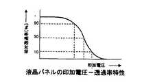
The cause of the poor gradation expression in the low-luminance part is the applied voltage-transmittance characteristics of the liquid crystal panel. As illustrated in FIG. 14, the applied voltage-transmittance characteristics of the liquid crystal panel are such that the change in transmittance with respect to the change in applied voltage is in a range where the transmittance is high (90% or more in the figure) (that is, a high luminance portion). On the other hand, in the range where the transmittance is low (in the figure, from 10% to 90%) (that is, the low luminance portion), the change in transmittance with respect to the change in applied voltage is steep. (The direction in which the applied voltage increases on the horizontal axis in FIG. 14 can be both leftward and rightward depending on the type of the liquid crystal panel).
[0007]
In addition, this applied voltage-transmittance characteristic has a high correlation with the thickness of the liquid crystal layer (that is, the size of the cell gap of the liquid crystal panel), and therefore, for each individual liquid crystal panel (and therefore for each individual liquid crystal projector device). There is some variation, and even one liquid crystal panel has some variation depending on the part. For this reason, it is difficult to finely adjust the luminance by controlling the applied voltage in the low luminance part (that is, the gradation expression is inferior).
[0008]
The disadvantage that the gradation expression in the low-brightness part is inferior appears not only when displaying a low-brightness image but also when lowering the brightness by operating the brightness adjustment button of the liquid crystal projector device. It was. That is, in the conventional liquid crystal projector apparatus, when the operation of lowering the brightness is performed with the brightness adjustment button, the applied voltage is changed so that the transmittance of the liquid crystal panel is lowered. -The gradation expression is also inferior due to the transmittance characteristic.
[0009]
Next, the cause of black floating is the pretilt angle (angle formed between the alignment film and liquid crystal molecules) on the alignment film on the electrode substrate of the liquid crystal panel. In the liquid crystal panel, even when the vibration direction of the incident linearly polarized light is not rotated (or rotated by 90 °) in the liquid crystal layer, the incident linearly polarized light may become elliptically polarized light due to the presence of the pretilt angle. . When this phenomenon occurs in the low-luminance portion, elliptically polarized light partially passes through the analyzer and enters the projection lens, and black float occurs and the contrast decreases.
[0010]
In the liquid crystal projector device, for the purpose of displaying a brighter image, the incident angle of light from the light source to the liquid crystal panel tends to be increased by decreasing the F number of the illumination optical system. It is known that the degree of contrast decrease due to pretilt becomes more significant as the angle increases. FIG. 15 illustrates the relationship between the degree of contrast reduction and the angle of incidence on the liquid crystal panel (referred to as “contrast viewing angle characteristics”). Regardless of the incident direction φ of light in the direction parallel to the panel surface of the liquid crystal panel, the contrast CR decreases as the incident angle θ increases. However, the contrast CR value with respect to the same incident angle θ value differs depending on the incident direction φ, and a line connecting the values of the incident angles θ with the same contrast CR value in all incident directions φ (“equal contrast” The line is referred to as a “line”) and has a shape approximating an ellipse or rectangle having an aspect ratio of about 1: 2.
[0011]
As described above, the conventional liquid crystal projector has the disadvantage that the gradation expression in the low luminance portion is inferior and the contrast is low. On the other hand, no attempt has been made to eliminate these drawbacks. For example, in Japanese Patent Laid-Open No. 6-102484, a light source having a variable light output level is provided, and the output level of the light source is reduced when the peak level of the video signal is lower than a predetermined reference level every predetermined period. In addition, a liquid crystal projector device is disclosed in which the liquid crystal panel is driven by increasing the level of the video signal.
[0012]
In this liquid crystal projector device, when the peak level of the video signal is lower than the reference level (that is, in the low luminance part), the output level of the light source is reduced, so that the amount of light projected onto the screen decreases and the level of the video signal Is increased to drive the liquid crystal panel, so that the transmittance of the liquid crystal panel is increased. Therefore, even in the low-luminance portion, the luminance can be finely adjusted using the range in which the change in transmittance with respect to the change in applied voltage is gentle among the applied voltage-transmittance characteristics shown in FIG. That is, gradation expression is improved).
[0013]
However, in this liquid crystal projector device, the amount of light projected onto the screen is reduced by providing a light source with a variable output level. In general, in a liquid crystal projector apparatus, a discharge lamp having a high luminous efficiency (such as an ultra-high pressure mercury lamp, a metal halide lamp or a xenon lamp) is often used as a light source. When the light output level of such a discharge lamp is made variable, This complicates the configuration of the power supply unit of the discharge lamp.
[0014]
In addition, in this liquid crystal projector device, the gradation expression is not improved when the luminance adjustment button of the liquid crystal projector device is operated to lower the luminance, rather than displaying an originally low luminance image.
[0015]
Further, in this liquid crystal projector device, when the output level of the light source is reduced, as shown in FIG. 16, the amount of light incident on the liquid crystal panel with a small incident angle on the liquid crystal panel is also large. The amount of light incident on the liquid crystal panel is also reduced equally. Therefore, even if the output level of the light source is reduced, light having a large incident angle to the liquid crystal panel (that is, light having a high degree of lowering the contrast due to the contrast viewing angle characteristics as shown in FIG. 15) is still liquid crystal to some extent. Since the light enters the panel, a decrease in contrast due to the occurrence of black float is not suppressed.
[0016]
In view of the above-described points, the present invention improves the gradation expression of a low-luminance part and suppresses a decrease in contrast due to the occurrence of black float without complicating the configuration of the light source in the liquid crystal projector apparatus. It was made as an issue to do.
[0017]
[Means for Solving the Problems]
In order to solve this problem, the applicant of the present invention modulates incident light to emit a liquid crystal panel, an illumination optical system that makes the emitted light from the light source enter the liquid crystal panel, and the emitted light from the liquid crystal panel. In a projection display device (that is, a liquid crystal projector device) having a projection optical system that leads to a screen, an optical shutter that blocks light in the order of large incident angles on the liquid crystal panel is either an illumination optical system or a projection optical system. It is arranged on one side, and the peak level of the video signal supplied from the outside is detected every predetermined period, and when the peak level is smaller than the predetermined reference level, the light is shut off by this optical shutter, and this video A device having a control means for driving the liquid crystal panel by increasing the signal level is proposed.
[0018]
In this liquid crystal projector device, an optical shutter that blocks light in the descending order of the incident angle to the liquid crystal panel is disposed in either the illumination optical system or the projection optical system. Then, the control means detects the peak level of the video signal supplied from the outside every predetermined period, and when the peak level is smaller than the predetermined reference level, the light is blocked by this optical shutter, When the level of the video signal is increased and the liquid crystal panel is driven, the transmittance of the liquid crystal panel is increased.
[0019]
As described above, in a period in which the peak level of the video signal supplied from the outside is lower than the reference level (that is, in a low-luminance portion), the amount of light projected onto the screen is reduced by blocking the light with the optical shutter, and The transmittance of the liquid crystal panel is increased.
[0020]
Therefore, the transmittance of the applied voltage-transmittance characteristic characteristic as shown in FIG. 14 is not affected by the complexity of the light source configuration by providing the light source having a variable output level even in the low luminance portion. The luminance can be finely adjusted (that is, the gradation expression is improved) using a range where the change is gentle (a range where the transmittance is high).
[0021]
In this liquid crystal projector device, since the optical shutter blocks light in the order of large incident angle to the liquid crystal panel, light with a high degree of lowering contrast from the contrast viewing angle characteristics as shown in FIG. More light is blocked than light with a low degree of lowering the contrast. As a result, the amount of light projected to the screen with a high degree of lowering the contrast is reduced more than the amount of light projected to the screen with a lower degree of lowering the contrast. It is suppressed.
[0022]
As an example, this optical shutter is used for the contrast viewing angle characteristics of liquid crystal panels.Based on ,The incident angle to the liquid crystal panel is large, It is preferable to configure so as to block light in order of decreasing degree of contrast. Thereby,Large incident angle on LCD panel Since the light having a higher degree of lowering the contrast is cut off by the optical shutter in order and is not projected onto the screen, the lowering of the contrast due to the occurrence of black float is further suppressed.
[0023]
Further, as an example, it is preferable that this optical shutter is disposed at either one of the approximate pupil position of the illumination optical system and the approximate pupil position of the projection optical system.
[0024]
Here, the cross-sectional shape of the light beam that passes through the pupil position of the optical system and the angular distribution of the light at the imaging position indicate that if the light beam passes through the optical system at the pupil position with an arbitrary cross-sectional shape, the image is formed. There is a relationship that the angular distribution of the light at the position is similar to the cross-sectional shape. Therefore, when this optical shutter is arranged at a substantially pupil position of the illumination optical system, the angular distribution of the light incident (imaged) on the liquid crystal panel is substantially similar to the cross-sectional shape of the light passing through the optical shutter. When the incident angle exceeds the angular distribution, no light enters the liquid crystal panel. Further, even when this optical shutter is disposed at a substantially pupil position of the projection optical system, an incident angle exceeding an angular distribution substantially similar to the cross-sectional shape of the light passing through the optical shutter out of the light incident on the liquid crystal panel. Even if the light is emitted from the liquid crystal panel, it does not pass through the optical shutter (thus, it is not projected onto the screen).
[0025]
Accordingly, in any case, by configuring the optical shutter so as to pass light having a circular cross-sectional shape, for example, it becomes easy to block light in the order of light having a large incident angle to the liquid crystal panel. By configuring the optical shutter to pass light having a cross-sectional shape substantially equal to the isocontrast line (see FIG. 15) of the panel, it becomes easy to block the light in the order of decreasing degree of contrast.
[0026]
Further, as an example, when the peak level is smaller than the reference level, the control means emits an amount of light corresponding to the value of (1-Vp / Vmax), with the peak level and the reference level being Vp and Vmax, respectively. It is preferable that the liquid crystal panel is driven by blocking with a shutter and increasing the level of a video signal supplied from outside by Vmax / Vp times.
[0027]
The brightness of the image projected from the liquid crystal panel through the projection lens onto the screen is determined by the product of the light transmission rate at this optical shutter and the rate of increase in the level of the video signal that drives the liquid crystal panel. Accordingly, in this way, an amount of light corresponding to the value of (1−Vp / Vmax) is blocked by the optical shutter (that is, an amount of light corresponding to the value of Vp / Vmax is passed by the optical shutter), and the liquid crystal panel By increasing the level of the video signal for driving the image by Vmax / Vp times, the brightness of the image projected on the screen does not block the light with this optical shutter, and the liquid crystal panel remains at the level of the original video signal Deviation from the brightness when driving is suppressed. (When the amount of light (1-Vp / Vmax) is blocked by the optical shutter, the optical shutter passing rate (Vp / Vmax) × level increase rate (Vmax / Vp) = 1), (The brightness of the image projected on the screen can be made the same as when the liquid crystal panel is driven while keeping the level of the original video signal while the light shutter does not block the light at all.)
[0028]
The optical shutter is configured to block light with a liquid crystal panel using twisted nematic liquid crystal, for example, or as another example, configured to block light with a liquid crystal panel using polymer dispersed liquid crystal. Is preferred.
[0029]
By blocking light with an optical shutter in such a liquid crystal panel, the optical shutter can be operated at a higher speed than when light is blocked with a mechanically operated component. Therefore, it is possible to quickly respond to a change in the level of the video signal and switch whether to block light or how much light is blocked.
[0030]
When an optical shutter is configured with such a liquid crystal panel, for example, it is preferable to use a liquid crystal panel having a plurality of concentric fixed pattern electrodes. This simplifies the structure and control of the optical shutter when the optical shutter is configured with a liquid crystal panel.
[0049]
DETAILED DESCRIPTION OF THE INVENTION
Hereinafter, embodiments of the present invention will be described with reference to the drawings.
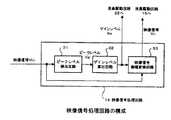
FIG. 1 shows a configuration example of a liquid crystal projector device according to the present invention. The optical system of the liquid crystal projector device includes a
[0050]
The
[0051]
In the illumination optical system 2, PBS (polarization beam splitter) 7 that passes P-polarized light and reflects S-polarized light out of the light emitted from the
[0052]
P-polarized light out of the light emitted from the
[0053]
As shown in FIG. 2, the arrangement of the reflecting
[0054]
As shown in FIG. 1, in the illumination optical system 2, a
[0055]
Each of the
[0056]
As shown in FIG. 2, the combined shape of all the lenses 10a and 11a is a rectangle having an aspect ratio of about 1: 2 (an aspect ratio substantially equal to the isocontrast line of the liquid crystal panel 3). The
[0057]
The shape of the lens 10a of the
[0058]
The microlens array 11 is disposed at a substantially focal position of the lens 10 a of the
[0059]
Here, in an optical system in which two microlens arrays and a condenser lens are arranged in order as in the illumination optical system 2, the position of the second microlens array is in the vicinity of the pupil position of the optical system (second The position slightly closer to the condenser lens than the microlens array is the pupil position). Therefore, in this liquid crystal projector device, the microlens array 11 is located in the vicinity of the pupil position of the illumination optical system 2.
[0060]
As shown in FIG. 3, the cross-sectional shape of the light beam passing through the pupil position of the optical system and the angular distribution of the light at the imaging position are arbitrary cross-sectional shapes (for example, rectangular) at the pupil position of the optical system. Or a circular beam), the angular distribution of the light at the imaging position is similar to the cross-sectional shape.
[0061]
The cross-sectional shape of the emitted light from the
[0062]
As shown in FIG. 1, the light emitted from each lens 11 a of the microlens array 11 enters the
[0063]
The shutter
[0064]
As shown in FIG. 4B, the fixed
[0065]
The shutter
[0066]
The liquid
[0067]
In the gain
[0068]
In the video signal
[0069]
A signal indicating the gain level Gs set by the gain
[0070]
(A) When Gs = 1, a driving voltage is applied so that light is transmitted through all the
(B) When 0.75 ≦ Gs <1, light is transmitted through the fixed
(C) When 0.5 ≦ Gs <0.75, light is transmitted through the portions of the fixed
(D) When 0.25 ≦ Gs <0.5, light is transmitted through the portions of the fixed
(E) When 0 <Gs <0.25, light is transmitted through the portion of the fixed
(F) When Gs = 0, a driving voltage is applied so that light is not transmitted through all the
[0071]
Therefore, in the
[0072]
In the high-luminance portion, a light beam whose cross-sectional shape is the contour shape of the outermost fixed pattern electrode 23e passes through the
[0073]
As described above, the
[0074]
In addition, the area of the light flux passing through the
[0075]
As shown in FIG. 1, the light that has passed through the
[0076]
A driving voltage corresponding to the level of the video signal Vc created by the video signal processing circuit 14 (FIG. 5) is applied from the liquid
[0077]
In the
[0078]
As shown in FIG. 1, the light transmitted through the
[0079]
Next, the operation of this liquid crystal projector device will be described.
When light is emitted from the
[0080]
The incident light on the
[0081]
Light emitted from the microlens array 11 enters the
Here, in the high luminance portion of the video signal Vin supplied from the outside to the liquid crystal projector device, the gain level Gs = 1 is set by the video signal processing circuit 14 (FIG. 5). Is not blocked at all. Accordingly, the cross-sectional shape of the light beam passing through the
[0082]
As a result, as shown in FIG. 7A, light is incident on the
[0083]
In this high luminance portion, since the gain level Gs = 1, the video signal Vc having the level as it is is generated by the video
[0084]
On the other hand, in the low luminance portion of the video signal Vin, the gain level Gs = Vp / Vmax is set by the video
[0085]
As a result, the
[0086]
In this low luminance portion, since the gain level Gs = Vp / Vmax, the video
[0087]
As described above, in this liquid crystal projector device, in the low luminance portion of the video signal Vin, the light is not projected onto the screen by being blocked by the
[0088]
Thereby, even in a low-luminance portion, the change in the applied voltage among the applied voltage-transmittance characteristic characteristics of the
[0089]
In the low-luminance portion of the video signal Vin, the light emitted from the microlens array 11 is emitted from the illumination optical system 2 in the order of light having a high degree of reduction in contrast according to the viewing angle characteristics of the
[0090]
Thereby, in the low-luminance part, the light having a higher degree of lowering the contrast is not incident on the liquid crystal panel 3 (that is, no longer projected onto the screen), so that the lowering of the contrast due to the occurrence of the black float is suppressed.
[0091]
In addition, since the
[0092]
The brightness of the image projected from the
[0093]
That is, when the value of the gain level Gs is just 0.8, 0.6, 0.4, and 0.2, the pass rate of the optical shutter is 80 as in (b) to (e) described above. %, 60%, 40%, and 20%, and the level of the video signal Vc is 1 / 0.8, 1 / 0.6, and 1 / 0.4, respectively, of the level of the video signal Vin. , 1 / 0.2 times, this passage rate × level increase rate = 1, so that the brightness of the image projected on the screen does not block the light by the
[0094]
Also, as shown in FIG. 4, the
[0095]
Further, since the liquid crystal panel having a plurality of concentric fixed pattern electrodes is used as the shutter liquid crystal panel, the structure and control of the
[0096]
In addition, in this liquid crystal projector device, the light emitted from the
[0097]
Further, in this liquid crystal projector device, the cross-sectional shape of the light beam obtained by combining the P-polarized light emitted from the
[0098]
As described above, the cross-sectional shape of the light emitted from the microlens array 11 approximates the isocontrast line of the
[0099]
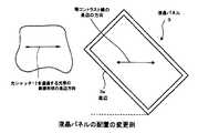
In the above example, the description has been given on the assumption that the direction of the long side of the isocontrast line of the
[0100]
FIG. 8 shows the shape of the
[0101]
FIG. 9 shows an arrangement example of the
[0102]
The
[0103]
In the above example, non-polarized light emitted from the
[0104]
In the above example, a light beam having a substantially elliptical cross-sectional shape having an aspect ratio substantially equal to the isocontrast line of the
[0105]
In FIG. 10, the
[0106]
The illumination optical system 16 of the liquid crystal projector device is provided with a microlens array 17, a microlens array 18, an
[0107]
In this liquid crystal projector device, the non-polarized light having the cross-sectional shape as it is emitted from the
[0108]
Further, in the above example, the video
[0109]
As a result, when the
[0110]
In the above example, the number of the fixed pattern electrodes of the shutter
[0111]
In the above example, the
[0112]
The polymer-dispersed liquid crystal is white turbid when no driving voltage is applied, and changes to transparent when the driving voltage is applied. When the drive voltage is not applied, the incident light to the polymer dispersed
[0113]
Unlike a liquid crystal panel using TN liquid crystal, a liquid crystal panel using this polymer dispersed liquid crystal does not require a polarizer or an analyzer. Therefore, if the
[0114]
Alternatively, the
[0115]
In the above example, the
[0116]
Alternatively, an optical shutter is provided at a position other than the pupil position in the illumination optical system 2 and the projection optical system, in accordance with the contrast viewing angle characteristics of the
[0117]
In the above example, an optical shutter is provided that blocks light in order of decreasing degree of contrast according to the contrast viewing angle characteristics of the
[0118]
In the above example, the video
[0119]
In the above example, the present invention is applied to a single-plate transmissive liquid crystal projector device. However, the present invention is applied to a three-plate transmissive liquid crystal projector device, a single-plate reflective liquid crystal projector device, and a three-plate reflective liquid crystal projector device. The present invention may also be applied.
[0120]
In the above example, the cross-sectional shape of the light emitted from the
[0121]
Even in that case, since light is emitted from both the
[0122]
As a result, the amount of incident light on the liquid crystal panel, which has a high degree of lowering the contrast, decreases from the contrast viewing angle characteristics of the liquid crystal panel as shown in FIG. It is suppressed.
[0123]
In the above example, the light emitted from the
[0124]
In the above example, the S-polarized light reflected by the
[0125]
Further, the present invention is not limited to the above examples, and it is needless to say that various other configurations can be taken without departing from the gist of the present invention.
[0126]
【The invention's effect】
As described above, according to the projection display device of the present invention, the configuration of the light source is complicated by providing the light source having a variable output level even in the low luminance portion of the video signal supplied from the outside. Therefore, there is an effect that the luminance can be finely adjusted (that is, the gradation expression can be improved).
[0127]
In the low-luminance portion, since the light having a large incident angle to the liquid crystal panel is blocked by the optical shutter and is not projected onto the screen, an effect of suppressing the decrease in contrast due to the occurrence of black float is obtained.
[0128]
In addition, if the optical shutter is configured to block in the order of light having a high degree of reducing the contrast in accordance with the contrast viewing angle characteristics of the liquid crystal panel, the light shutter is blocked in the order of light having the high degree of reducing the contrast and is blocked on the screen. Since it is not projected, the effect that the reduction in contrast due to the occurrence of black float can be further suppressed can be obtained.
[0129]
In addition, if the optical shutter is arranged at one of the approximate pupil position of the illumination optical system and the approximate pupil position of the projection optical system, the light is blocked in the order of the light having the large incident angle to the liquid crystal panel, and the contrast is reduced. It is also possible to obtain an effect that it becomes easy to block the light in the descending order of the degree of light.
[0130]
In addition, when the peak level is smaller than the reference level, the control means sets the peak level and the reference level to Vp and Vmax, and blocks the amount of light corresponding to the value of (1−Vp / Vmax) with the optical shutter. In addition, if the liquid crystal panel is driven by increasing the level of the video signal supplied from the outside by Vmax / Vp times, the brightness of the image projected on the screen does not block the light with the optical shutter. There is also an effect that it is possible to suppress deviation from the brightness when the liquid crystal panel is driven with the original video signal level.
[0131]
In addition, if the optical shutter is configured to block light on the liquid crystal panel, it responds quickly to changes in the level of the video signal and switches whether to block light or how much light is blocked. The effect that it can be also obtained.
[0132]
In addition, when a liquid crystal panel having a plurality of concentric fixed pattern electrodes is used, an effect that the structure and control of the optical shutter when the optical shutter is configured by the liquid crystal panel can be simplified.
[0133]
Next, according to the projection type display device of the present invention, when the brightness adjusting operation means is operated so as to lower the brightness, the configuration of the light source is complicated by providing a light source having a variable output level. There is an effect that gradation expression can be improved without incurring.
[0134]
And since it is interrupted | blocked in order of the light with a large incident angle to a liquid crystal panel, and is no longer projected on a screen, the effect that the fall of contrast by generation | occurrence | production of a black float can be suppressed is acquired.
[0135]
Next, according to the projection type display device according to the present invention, the output level of the output level is reduced by blocking light with an optical shutter that blocks light in order of decreasing degree of contrast according to the contrast viewing angle characteristics of the liquid crystal panel. By providing a variable light source, the gradation expression of the low-luminance portion can be improved without complicating the configuration of the light source.
[0136]
And, according to the contrast viewing angle characteristics of the liquid crystal panel, since the light with a high degree of reducing the contrast is cut off in order and is not projected on the screen, the effect of reducing the contrast due to the occurrence of black floating can be suppressed very well Is obtained.
[0137]
Next, according to the projection type display device of the present invention, it is possible to suppress the decrease in contrast due to the occurrence of black floating, and the use efficiency of the emitted light from the light source without incurring the complexity and cost of the optical system. It is possible to obtain an effect that a brighter image can be displayed on the screen.
[Brief description of the drawings]
FIG. 1 is a diagram showing a configuration example of a liquid crystal projector device of the present invention.
2 is a diagram showing the transmitted light of the PBS of FIG. 1 and the emitted light of the half-
FIG. 3 is a diagram showing the relationship between the cross-sectional shape of a light beam passing through the pupil position of the optical system and the angular distribution of the light at the imaging position.
4 is a diagram illustrating a configuration example of the optical shutter in FIG. 1;
5 is a diagram illustrating a configuration example of a video signal processing circuit in FIG. 1. FIG.
6 is a view showing a state of blocking incident light by the optical shutter of FIG. 1. FIG.
7 is a diagram showing an angular distribution of incident light on the liquid crystal panel of FIG. 1. FIG.
FIG. 8 is a diagram showing a modification of the microlens array of FIG.
FIG. 9 is a diagram illustrating a modification example of the arrangement of the liquid crystal panel of FIG. 1;
FIG. 10 is a diagram showing another configuration example of the liquid crystal projector apparatus of the present invention.
FIG. 11 is a diagram showing another configuration example of the liquid crystal projector device of the present invention.
FIG. 12 is a diagram showing light emitted from a polymer-dispersed liquid crystal when no voltage is applied.
FIG. 13 is an example showing a configuration example of an optical system of a conventional liquid crystal projector apparatus.
FIG. 14 is a diagram illustrating an applied voltage-transmittance characteristic characteristic of a liquid crystal panel.
FIG. 15 is a diagram illustrating contrast viewing angle characteristics of a liquid crystal panel.
FIG. 16 is a diagram showing how light is reduced by a light source having a variable light output level.
[Explanation of symbols]
DESCRIPTION OF
Claims (7)
Translated fromJapanese前記液晶パネルへの入射角の大きい光の順に遮断する光シャッタを、前記照明光学系と前記投射光学系とのいずれか一方に配置し、
所定期間毎に、外部から供給される映像信号のピークレベルを検出し、該ピークレベルが所定の基準レベルよりも小さい場合に、前記光シャッタで光を遮断させるとともに、該映像信号のレベルを増大させて前記液晶パネルを駆動させる制御手段を備えた
投射型表示装置。A projection type display device having a liquid crystal panel that modulates and emits incident light, an illumination optical system that causes the light emitted from a light source to enter the liquid crystal panel, and a projection optical system that guides the light emitted from the liquid crystal panel to a screen In
An optical shutter that blocks in order of light having a large incident angle to the liquid crystal panel is disposed in one of the illumination optical system and the projection optical system,
The peak level of the video signal supplied from the outside is detected every predetermined period, and when the peak level is smaller than the predetermined reference level, the light is blocked by the optical shutter and the level of the video signal is increased. Control means for driving the liquid crystal panel
Throw Cum-type display device.
前記光シャッタは、前記液晶パネルのコントラスト視野角特性に基づき、前記液晶パネルへの入射角が大きく、コントラストを低下させる度合いの大きい光の順に遮断する
投射型表示装置。The projection display device according to claim 1,
Based on the contrast viewing angle characteristics of the liquid crystal panel, the optical shutter blocks light in the order of light having a largeincident angle on the liquid crystal panel and a large degree of decreasingthe contrast.
Throw Cum-type display device.
前記光シャッタは、前記照明光学系の略瞳位置と前記投射光学系の略瞳位置とのいずれか一方に配置されている
投射型表示装置。In the projection type display device according to claim 1 or 2,
The optical shutter is disposed at either one of a substantially pupil position of the illumination optical system and a substantially pupil position of the projection optical system.
Throw Cum-type display device.
前記制御手段は、前記ピークレベルが前記基準レベルよりも小さい場合に、該ピークレベル,該基準レベルをそれぞれVp,Vmaxとして、(1−Vp/Vmax)の値に応じた量の光を前記光シャッタで遮断させるとともに、前記映像信号のレベルをVmax/Vp倍に増大させて前記液晶パネルを駆動させる
投射型表示装置。In the projection type display apparatus in any one of Claims 1 thru | or 3,
When the peak level is smaller than the reference level, the control means sets the peak level and the reference level to Vp and Vmax, and emits an amount of light corresponding to a value of (1−Vp / Vmax). The liquid crystal panel is driven by blocking with a shutter and increasing the level of the video signal by Vmax / Vp times.
Throw Cum-type display device.
前記光シャッタは、ネマティック液晶を用いた液晶パネルで光を遮断する
投射型表示装置。In the projection type display apparatus in any one of Claims 1 thru | or 4,
The optical shutter blocks light with a liquid crystal panel using nematic liquid crystal.
Throw Cum-type display device.
前記光シャッタは、高分子分散液晶を用いた液晶パネルで光を遮断する
投射型表示装置。In the projection type display apparatus in any one of Claims 1 thru | or 4,
The optical shutter blocks light with a liquid crystal panel using polymer dispersed liquid crystal.
Throw Cum-type display device.
前記液晶パネルは、複数の同心の固定パターン電極を有する
投射型表示装置。In the projection type display device according to claim 5 or 6,
The liquid crystal panel has a plurality of concentric fixed pattern electrodes.
Throw Cum-type display device.
Priority Applications (1)
| Application Number | Priority Date | Filing Date | Title |
|---|---|---|---|
| JP2000074366AJP4337222B2 (en) | 2000-03-16 | 2000-03-16 | Projection display |
Applications Claiming Priority (1)
| Application Number | Priority Date | Filing Date | Title |
|---|---|---|---|
| JP2000074366AJP4337222B2 (en) | 2000-03-16 | 2000-03-16 | Projection display |
Publications (2)
| Publication Number | Publication Date |
|---|---|
| JP2001264728A JP2001264728A (en) | 2001-09-26 |
| JP4337222B2true JP4337222B2 (en) | 2009-09-30 |
Family
ID=18592437
Family Applications (1)
| Application Number | Title | Priority Date | Filing Date |
|---|---|---|---|
| JP2000074366AExpired - Fee RelatedJP4337222B2 (en) | 2000-03-16 | 2000-03-16 | Projection display |
Country Status (1)
| Country | Link |
|---|---|
| JP (1) | JP4337222B2 (en) |
Families Citing this family (15)
| Publication number | Priority date | Publication date | Assignee | Title |
|---|---|---|---|---|
| US6947025B2 (en) | 2001-10-09 | 2005-09-20 | Seiko Epson Corporation | Lighting apparatus and projection type display, and driving method therefore |
| US7136035B2 (en) | 2001-12-11 | 2006-11-14 | Seiko Epson Corporation | Projection type display, a display and a drive method thereof |
| US20050213044A1 (en)* | 2002-03-14 | 2005-09-29 | Koninklijke Philips Electronics N.V. | Projection device having a mode selection unit |
| US7220006B2 (en) | 2003-08-08 | 2007-05-22 | Allen Eddie E | Method and apparatus for increasing effective contrast ratio and brightness yields for digital light valve image projectors |
| JP2005203859A (en)* | 2004-01-13 | 2005-07-28 | Olympus Corp | Projector |
| JP2005215475A (en)* | 2004-01-30 | 2005-08-11 | Seiko Epson Corp | projector |
| JP4539099B2 (en)* | 2004-02-03 | 2010-09-08 | セイコーエプソン株式会社 | Projection type display device, control method for projection type display device, and image output device |
| KR100670008B1 (en)* | 2004-11-26 | 2007-01-19 | 삼성전자주식회사 | Optical engine, projection apparatus having same and optical engine control method of projection apparatus |
| US7226172B2 (en)* | 2005-01-12 | 2007-06-05 | Colorlink, Inc. | Illumination attenuation system |
| JP4839672B2 (en)* | 2005-02-03 | 2011-12-21 | 株式会社ニコン | Display device |
| JP4158776B2 (en) | 2005-03-09 | 2008-10-01 | セイコーエプソン株式会社 | Image display device and projector |
| JP2008292725A (en)* | 2007-05-24 | 2008-12-04 | Sanyo Electric Co Ltd | Illumination apparatus and projection type image display apparatus |
| JP5267250B2 (en)* | 2009-03-18 | 2013-08-21 | セイコーエプソン株式会社 | Light control device and lighting device for projector using the light control device |
| JP5343917B2 (en)* | 2010-04-22 | 2013-11-13 | 株式会社Jvcケンウッド | Video display device |
| JP5793691B2 (en)* | 2010-07-02 | 2015-10-14 | パナソニックIpマネジメント株式会社 | Projection display device |
- 2000
- 2000-03-16JPJP2000074366Apatent/JP4337222B2/ennot_activeExpired - Fee Related
Also Published As
| Publication number | Publication date |
|---|---|
| JP2001264728A (en) | 2001-09-26 |
Similar Documents
| Publication | Publication Date | Title |
|---|---|---|
| US6854851B2 (en) | Projection display | |
| JP5191771B2 (en) | Surface illumination device and liquid crystal display device using the same | |
| JP4337222B2 (en) | Projection display | |
| CN1936698B (en) | Lighting apparatus and projection type display, and driving method therefore | |
| US7226172B2 (en) | Illumination attenuation system | |
| JP3019574B2 (en) | Projection display device | |
| KR100394283B1 (en) | Presentation system with overhead projector | |
| US7385565B2 (en) | Projection-type display apparatus | |
| JPH05241103A (en) | Projection type liquid crystal display device | |
| US9028074B2 (en) | Image display system and control apparatus | |
| JP2001249400A (en) | Projection display device | |
| JP2005024686A (en) | Projection type video display device | |
| JP3473557B2 (en) | Lighting device and projector | |
| JP2003107422A (en) | Liquid crystal projector | |
| JP3791377B2 (en) | Liquid crystal display element and display device using the same | |
| JP4082027B2 (en) | Illumination device and projector using the same | |
| JPH0554677B2 (en) | ||
| JP2001264727A (en) | Projection type display device | |
| JP3654798B2 (en) | Image display device and lighting device | |
| JP2001343623A (en) | Liquid crystal projector device and method for improving contrast | |
| JP4396213B2 (en) | Image display device | |
| KR100293103B1 (en) | LCD Display | |
| TWI892011B (en) | Projection system | |
| WO2005060268A1 (en) | Brightness regulation in lcd projection systems | |
| US20030201961A1 (en) | Projection system and method for reflection-type liquid crystal display |
Legal Events
| Date | Code | Title | Description |
|---|---|---|---|
| A621 | Written request for application examination | Free format text:JAPANESE INTERMEDIATE CODE: A621 Effective date:20061221 | |
| A977 | Report on retrieval | Free format text:JAPANESE INTERMEDIATE CODE: A971007 Effective date:20080922 | |
| A131 | Notification of reasons for refusal | Free format text:JAPANESE INTERMEDIATE CODE: A131 Effective date:20080930 | |
| A521 | Written amendment | Free format text:JAPANESE INTERMEDIATE CODE: A523 Effective date:20081201 | |
| TRDD | Decision of grant or rejection written | ||
| A01 | Written decision to grant a patent or to grant a registration (utility model) | Free format text:JAPANESE INTERMEDIATE CODE: A01 Effective date:20090609 | |
| A01 | Written decision to grant a patent or to grant a registration (utility model) | Free format text:JAPANESE INTERMEDIATE CODE: A01 | |
| A61 | First payment of annual fees (during grant procedure) | Free format text:JAPANESE INTERMEDIATE CODE: A61 Effective date:20090622 | |
| FPAY | Renewal fee payment (event date is renewal date of database) | Free format text:PAYMENT UNTIL: 20120710 Year of fee payment:3 | |
| FPAY | Renewal fee payment (event date is renewal date of database) | Free format text:PAYMENT UNTIL: 20130710 Year of fee payment:4 | |
| R250 | Receipt of annual fees | Free format text:JAPANESE INTERMEDIATE CODE: R250 | |
| R250 | Receipt of annual fees | Free format text:JAPANESE INTERMEDIATE CODE: R250 | |
| LAPS | Cancellation because of no payment of annual fees |