JP4336232B2 - Touch panel - Google Patents
Touch panelDownload PDFInfo
- Publication number
- JP4336232B2 JP4336232B2JP2004096230AJP2004096230AJP4336232B2JP 4336232 B2JP4336232 B2JP 4336232B2JP 2004096230 AJP2004096230 AJP 2004096230AJP 2004096230 AJP2004096230 AJP 2004096230AJP 4336232 B2JP4336232 B2JP 4336232B2
- Authority
- JP
- Japan
- Prior art keywords
- film
- touch panel
- transparent conductive
- conductive film
- protective sheet
- Prior art date
- Legal status (The legal status is an assumption and is not a legal conclusion. Google has not performed a legal analysis and makes no representation as to the accuracy of the status listed.)
- Expired - Fee Related
Links
Images


Classifications
- G—PHYSICS
- G06—COMPUTING OR CALCULATING; COUNTING
- G06F—ELECTRIC DIGITAL DATA PROCESSING
- G06F3/00—Input arrangements for transferring data to be processed into a form capable of being handled by the computer; Output arrangements for transferring data from processing unit to output unit, e.g. interface arrangements
- G06F3/01—Input arrangements or combined input and output arrangements for interaction between user and computer
- G06F3/03—Arrangements for converting the position or the displacement of a member into a coded form
- G06F3/041—Digitisers, e.g. for touch screens or touch pads, characterised by the transducing means
- G06F3/045—Digitisers, e.g. for touch screens or touch pads, characterised by the transducing means using resistive elements, e.g. a single continuous surface or two parallel surfaces put in contact
Landscapes
- Engineering & Computer Science (AREA)
- General Engineering & Computer Science (AREA)
- Theoretical Computer Science (AREA)
- Human Computer Interaction (AREA)
- Physics & Mathematics (AREA)
- General Physics & Mathematics (AREA)
- Position Input By Displaying (AREA)
- Push-Button Switches (AREA)
Description
Translated fromJapanese本発明はタッチパネルに係り、特に、PDA(Personal Digital assistant)、ノート型パーソナルコンピュータ等において液晶パネルの表示面上に配置されて表示面にペンを使用して直接入力する入力デバイスとして用いられるタッチパネルであり、X−Y座標の検出原理がアナログ抵抗膜式であって、入力点の座標の検出方式が一般的であるペン入力型アナログ抵抗膜式のタッチパネルに関する。 The present invention relates to a touch panel, and more particularly to a touch panel that is arranged on a display surface of a liquid crystal panel in a PDA (Personal Digital assistant), a notebook personal computer, and the like and is used as an input device that directly inputs a display surface using a pen. Further, the present invention relates to a pen input type analog resistance film type touch panel in which the detection principle of XY coordinates is an analog resistance film type and the detection method of the coordinates of an input point is general.
PDA、ノート型パーソナルコンピュータ等の小型であることが要求される電子機器においては、タッチパネルについてもサイズが小型であることが要求される。タッチパネルのサイズを小型化には、入力点の座標の検出方式が一般的なものであることが望ましい。ガラス板の周囲のデッドスペースを小さく出来るからである。なお、一般的な入力点の座標の検出方式は、X座標の検出はフィルム上の透明導電膜の電位勾配を利用し、Y座標の検出はガラス板上の透明導電膜の電位勾配を利用して行う方式である。 In electronic devices that are required to be small, such as PDAs and notebook personal computers, the touch panel is also required to be small in size. In order to reduce the size of the touch panel, it is desirable that the coordinate detection method of the input point is a general one. This is because the dead space around the glass plate can be reduced. As a general input point coordinate detection method, X coordinate detection uses the potential gradient of the transparent conductive film on the film, and Y coordinate detection uses the potential gradient of the transparent conductive film on the glass plate. This is a method to be performed.
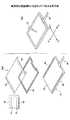
図1及び図2は従来の入力点の座標の検出方式が一般的であるペン入力型アナログ抵抗膜式のタッチパネル10を示す。Xは長い辺に沿う方向、Yは短い辺に沿う方向である。タッチパネル10は、基板である四角形状のガラス板11の上面に、フィルム20が枠状の両面接着テープ19によって接着してあり、フィルム20が空気層18を介してガラス板11を覆っており、フレキシブルケーブル16が延びている構成である。ガラス板11の上面には、透明導電膜12が形成してあり、且つ、多数のドットスペーサ13が分散して形成してあり、且つY方向上対向する辺に沿って細長い電極14,15が形成してある。フィルム20は、PET(Polyethylene terephthalate)フィルム本体21の下面に透明導電膜22が密着して形成してあり、且つPETフィルム本体21の上面にハードコート層としてのアクリル樹脂層23がPETフィルム本体21の表面を保護するために形成してあり、且つ、X方向上対向する辺に沿って細長い電極24,25が形成してある構成である。 FIG. 1 and FIG. 2 show a pen input type analog resistance film
タッチパネル10は図2に示すように液晶パネル30の上面に搭載されて且つカバー31で周囲を覆われて、PDAを構成する。操作者はポリアセタール製のペン35を使用して、フィルム20の上面に文字を書いたり、フィルム20の上面の所定の場所を押し付けたりする入力操作を行う。 As shown in FIG. 2, the
ペン35を押し付けると、図2中、二点鎖線で示すように、フィルム20が撓んで、ペン35を押し付けた位置のフィルム20の透明導電膜22がガラス板11の透明導電膜12に接触する。 When the
電極14,15間に電圧を印加するとフィルム20の透明導電膜22によってX方向に電位勾配ができ、接触点の電位がガラス板11の透明導電膜12を通じて検出され、所定の分圧を表す数式から、押し付け点(接触点)のX座標が分かる。電極24,25間に電圧を印加するとガラス板11の透明導電膜12によってY方向に電位勾配ができ、接触点の電位がフィルム20の透明導電膜22を通じて検出され、所定の分圧を表す数式から、押し付け点(接触点)のY座標が分かる。
ここで、透明導電膜12、22は硬い物質であるため、物理的作用によって剥離や亀裂を起こしやすい性質がある。ここで、フィルム20はペン35によって押し付けられる場所が撓まされるため、撓まされた場所のフィルム20上の透明導電膜22は引っ張り応力を作用され、PDAを長く使用しているうちに、徐々に剥離や亀裂が発生する。フィルム20上の透明導電膜22に剥離や亀裂が発生すると、透明導電膜22の抵抗分布が変化し、ペン35を押し付けた位置のX座標とタッチパネル10から出力される信号としてのX座標との間に誤差が発生し出して、タッチパネル10に要求される特性の一つであるリニアリティが低下してリニアリティを表す数値が増加する。市場が要求するリニアリティは例えば1%以下である。よって、PDAの使用期間が長くなると、リニアリティの低下が現われ、リニアリティが仕様から外れる程度にまで低下すると、PDAがペンの操作とは異なった動作を起こすようになり、タッチパネル10は寿命に到る。なお、PDAを通常に使用している限りにおいては、タッチパネル10の寿命は十分に長く、特に問題はない。 Here, since the transparent
本発明者は、PDAを使用している人を観察して、操作者の癖にもよるところであるけれども、例えば電話等をしながら入力目的ではなくて無意識にペン35をカバー31の縁に沿って往復移動させてタッチパネル10の同じ個所を直線を描くように往復させて繰り返して擦る操作が行われていることが分かった。この操作はタッチパネル10を傷める苛酷な操作である。 The present inventor observes the person using the PDA and depends on the operator's habit. For example, while making a call or the like, the inventor unconsciously moves the
このようなタッチパネル10にとって苛酷な操作がなされると、フィルム20上の透明導電膜22に比較的早期に剥離や亀裂が発生してしまい、リニアリティが低下してタッチパネル10は予定よりも早くに寿命となってしまう。 When such a severe operation is performed on the
図1中、40は従来のタッチパネル用保護シートを示す。タッチパネル用保護シートは、PDAのオプション部品の一つであり、タッチパネルの表面に傷及び汚れ等が付かないようにタッチパネルの表面を保護するべく、図2に示すように、タッチパネルの表面に貼り付けられて使用され、特に、使用環境が厳しい屋外設置端末や、ファーストフード店用端末、厨房用端末等で使用される。汚れた場合には、剥がして、新しいものと交換される。貼り付け、剥がしは、PDAのユーザが行う。従来の保護シート40は、その全面に粘着層部41を有する構成である。このため、貼り付けのときに、空気が閉じ込められた気泡が形成され易くなり、この気泡が目だってしまうという問題があった。また、従来の保護シート40は、タッチパネルの表面を保護するだけであり、他の働きはなかった。 In FIG. 1,
本発明は、上記の点に鑑みなされたものであり、苛酷な操作に耐え得るタッチパネルを提供することを目的とする。 The present invention has been made in view of the above points, and an object of the present invention is to provide a touch panel that can withstand severe operations.
そこで、上記課題を解決するため、本発明は、フィルム本体の裏面に透明導電膜を有し表面側をペンによって押され或いは擦られて操作されるフィルムを備えたタッチパネルにおいて、該フィルムは、該フィルム本体の表面に、耐熱アクリル系樹脂製の表面層を有し、該フィルム本体の裏面側については、耐熱アクリル系樹脂製の裏面層を有し、該裏面層の下面に前記透明導電膜を有することを特徴とする。To solve the above problems, the present invention provides a touch panel having a film which is operated surface side has a transparent conductive film on the back surfaceof the film body is pressed by the pen or rubbed with, the film,the The surface of the film body has a surface layer made of heat-resistant acrylic resin, and the back side of the film body has a back surface layer made of heat-resistant acrylic resin, and the transparent conductive film is formed on the lower surface of the back surface layer. It is characterized byhaving .
本発明によれば、フィルム本体の表面に耐熱アクリル系樹脂製の表面層を有し、且つ、フィルム本体の裏面側に耐熱アクリル系樹脂製の裏面層を有することによって、フィルムはペンを操作したときの摩擦熱の発生を抑制する構造を有するようになり、ペンで同じ個所を繰り返してなぞる操作を行った場合であっても、透明導電膜のうちペンを操作した個所に作用する熱応力を従来に比べて抑えることが出来、よって、透明導電膜の劣化の進行を抑えることが出来る。これによって、タッチパネルのリニアリティが長期に亘って良好に維持され、タッチパネルの長寿命化を達成することが出来る。According to the present invention, thefilm has a surface layer made of a heat-resistant acrylic resin on the surface of the film body, and the film has a pen operatedby having a back layer made of heat-resistant acrylic resin on the back side of the film body . heat acting on the point of generation of frictional heatbecomes so that the have a suppressingstructure, even when performing the operation of tracing repeat the same place with the pen, which operates the pen of the transparent conductive film when The stress can be suppressed as compared with the conventional case, and thus the progress of the deterioration of the transparent conductive film can be suppressed. As a result, the linearity of the touch panel is well maintained over a long period of time, and the life of the touch panel can be extended.
次に本発明の実施の形態について説明する。 Next, an embodiment of the present invention will be described.
説明の便宜上、解決手段を突き止めるための実験について説明する。 For convenience of explanation, an experiment for ascertaining a solution will be described.
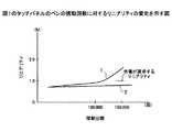
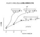
先ずは、25℃である通常の温度環境下で、図1の従来のタッチパネル10に対してペン35で同じ個所を往復させて繰り返して擦る操作を行って、リニアリティの増加の進み具合を見てみた。この場合には、リニアリティは、図3中、線Iで示すように、徐々に増加して、擦る回数が10万回を越えると、1%を越えてしまう。 First, in a normal temperature environment of 25 ° C., an operation of reciprocating and rubbing the same portion with the
上記と同じ実験を−10℃である低温度環境下で行った。この場合には、リニアリティは、図3中、線IIで示すように、擦る回数が増えても初期の状態に保たれ、擦る回数が10万回を越えても、1%以下に維持されていた。 The same experiment as described above was performed in a low temperature environment of −10 ° C. In this case, as indicated by line II in FIG. 3, the linearity is maintained in the initial state even when the number of rubbing increases, and is maintained at 1% or less even when the number of rubbing exceeds 100,000. It was.
これは、環境温度が25℃である場合には、PETフィルム本体21のうちペン35が擦る部分に摩擦熱が発生してその部分が熱膨張し、熱膨張した部分に対応する透明導電膜22に引張応力が作用し、これが原因で透明導電膜22に剥離や亀裂が発生し、これに対して、環境温度が−10℃である場合には、温度が−10℃と低温であるため、PETフィルム本体21のうちペン35が擦る部分に摩擦熱が発生しても直ぐに冷却されてしまい、PETフィルム本体21が熱膨張を起こさず、よって、透明導電膜22に引張応力が発生しないためであると理解出来る。 This is because, when the environmental temperature is 25 ° C., frictional heat is generated in the portion of the PET film
即ち、透明導電膜22に剥離や亀裂が発生することを抑制するには、透明導電膜22の厚みを厚くするなどして透明導電膜22の機械的強度を上げることが有効であるように考えるのが一般的であるが、これは誤りであり、透明導電膜22の厚さを厚くしても問題は解決出来ず、PETフィルム本体21の熱による膨張を抑えることによって、問題が解決出来ることが分かった。 That is, it is considered effective to increase the mechanical strength of the transparent
本発明は上記の実験の結果に基づくものである。 The present invention is based on the results of the above experiments.
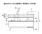
図4及び図5は本発明の実施例1になるタッチパネル50を示す。タッチパネル50は、入力点の座標の検出方式が一般的なものであって、且つ、ペン入力型であってアナログ抵抗膜式である。タッチパネル50は、PETフィルム本体61の上面のハードコート層が、耐熱アクリル系樹脂の層63である点が、図1及び図2に示すタッチパネル10とは相違する。X1−X2は長い辺に沿う方向、Y1−Y2は短い辺に沿う方向である。タッチパネル50は、基板である四角形状のガラス板51の上面に、フィルム60が枠状の両面接着テープ59によって接着してあり、フィルム60が空気層58を介してガラス板51を覆っており、フレキシブルケーブル56が延びている構成である。ガラス板51の上面には、透明導電膜(ITO膜)52が形成してあり、且つ、多数のドットスペーサ53が分散して形成してあり、且つY方向上対向する辺に沿って細長い電極54,55が形成してある。フィルム60は、PETフィルム本体61の下面に透明導電膜(ITO膜)62が密着して形成してあり、且つPETフィルム本体61の上面にハードコート層としての耐熱アクリル系樹脂の層63がPETフィルム本体61の表面を保護するために形成してあり、且つ、X方向上対向する辺に沿って細長い電極64、65が形成してある構成である。層63を構成する耐熱アクリル系樹脂は、100℃時の加熱収縮率が0.5%以下であり、ポリアセタール製のペン75に対する摩擦係数が1.0以下(ASTMD(American Society for Testing and Materials D)1894)である。4 and 5 show the
タッチパネル50は図5に示すように液晶パネル70の上面に搭載されて且つカバー71で周囲を覆われて、PDA72を構成する。操作者はポリアセタール製のペン75を使用して、フィルム60の上面に文字を書いたり、フィルム60の上面の所定の場所を押し付けたりする入力操作を行う。 The
ペン75を押し付けると、図5中、二点鎖線で示すように、フィルム60が撓んで、ペン75を押し付けた位置のフィルム60の透明導電膜62がガラス板51の透明導電膜52に接触する。 When the
電極54,55間に電圧を印加するとフィルム60の透明導電膜62によってX方向に電位勾配ができ、接触点の電位がガラス板51の透明導電膜52を通じて検出され、所定の分圧を表す数式から、押し付け点(接触点)のX座標が分かる。電極64,65間に電圧を印加するとガラス板51の透明導電膜52によってY方向に電位勾配ができ、接触点の電位がフィルム60の透明導電膜62を通じて検出され、所定の分圧を表す数式から、押し付け点(接触点)のY座標が分かる。 When a voltage is applied between the
次に、ペン75でもってタッチパネル50の同じ個所を往復させて繰り返して擦る操作をおこなった場合について説明する。 Next, the case where the
通常のアクリル系樹脂層はポリアセタール製のペン75に対する摩擦係数が1.0より大きいのに対して、耐熱アクリル系樹脂層63はポリアセタール製のペン75に対する摩擦係数が1.0以下と従来に比べて小さいため、摩擦熱の発生が抑えられ、よって、PETフィルム本体61の熱膨張が抑えられ、よって透明導電膜62に作用する応力が抑えられる。これによって、透明導電膜62に剥離や亀裂が発生することが抑制される。 While the normal acrylic resin layer has a friction coefficient with respect to the
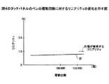
25℃の温度環境下で、図4及び図5に示すタッチパネル50に対してペン75で同じ個所を往復させて繰り返して擦る操作を行って、リニアリティの増加の進み具合を見てみた。この場合には、リニアリティは、図6中、線IIIで示すように、初期の状態に保たれ、擦る回数が10万回を越えても、1%以下に維持されていた。 Under the temperature environment of 25 ° C., the
図7は本発明の実施例2になるタッチパネル50Aを示す。タッチパネル50Aは、図4及び図5に示すタッチパネル50とは、フィルム60Aが相違する。フィルム60Aは、PETフィルム本体61の下面に透明導電膜62が密着して形成してあり、且つPETフィルム本体61の上面に、耐熱アクリル系樹脂層81及びアクリル樹脂層83の順で重ねて形成してある構造である。フィルム60Aは、図4に示すフィルム60と比較すると、アクリル樹脂層83を追加して有する構造であり、図1に示すフィルム20と比較すると、アクリル樹脂層83とPETフィルム本体61との間に、耐熱アクリル系樹脂層81を追加して有する構造である。FIG. 7 shows a
耐熱アクリル系樹脂層81は、ペン75の繰り返し操作によってアクリル樹脂層83に局部的に発生した摩擦熱を、フィルム60Aの面方向に熱伝導させて分散させる働きをする。 The heat-resistant
よって、PETフィルム本体61の局部的な熱膨張が抑えられ、よって透明導電膜62に作用する応力が抑えられる。これによって、透明導電膜62に剥離や亀裂が発生することが抑制される。 Therefore, local thermal expansion of the PET film
図8は本発明の実施例3になるタッチパネル50Bを示す。タッチパネル50Bは、図4及び図5に示すタッチパネル50とは、フィルム60Bが相違する。フィルム60Bは、PETフィルム本体61Bの下面に透明導電膜62が密着して形成してあり、且つPETフィルム本体61Bの上面にアクリル樹脂層83が形成してあり、PETフィルム本体61Bの厚さtは、従来が200μmよりも薄いのに対して、厚さを増して200〜500μmである構造である。 FIG. 8 shows a
フィルム60Bは、図1に示すPETフィルム本体21と比較すると、PETフィルム本体61Bの厚さが二倍程度に厚くなっている構造である。The
厚みのあるPETフィルム本体61Bは、ペン75の繰り返し操作によってアクリル樹脂層83に局部的に発生した摩擦熱を、フィルム60Bの面方向や厚み方向に熱伝導させて分散させる働きをする。The thick
よって、PETフィルム本体61Bの局部的な熱膨張が抑えられ、よって透明導電膜62には応力が局部的に集中して作用することが回避され、これによって、透明導電膜62に剥離や亀裂が発生することが抑制される。 Therefore, local thermal expansion of the PET film
図9は本発明の実施例4になるタッチパネル50Cを示す。タッチパネル50Cは、図4及び図5に示すタッチパネル50とは、フィルム60Cが相違する。フィルム60Cは、耐熱PETフィルム本体61Cの下面に透明導電膜62が密着して形成してあり、且つ耐熱PETフィルム本体61Cの上面に、アクリル樹脂層83が形成してある構造である。フィルム60Cは、図1に示すフィルム20と比較すると、PETフィルム本体21に代えて、耐熱PETフィルム本体61Cを有する構造である。FIG. 9 shows a touch panel 50C according to the fourth embodiment of the present invention. The touch panel 50C is different from the
耐熱PETフィルム本体61Cは、100℃時の加熱収縮率が0.5%以下であり、ポリアセタール製のペン75に対する摩擦係数が1.0以下(ASTMD1894)である
耐熱PETフィルム本体61Cは、ペン75の繰り返し操作によってアクリル樹脂層83に局部的に発生した摩擦熱を、フィルム60Cの面方向に熱伝導させて分散させる働きをする。The heat-resistant
よって、PETフィルム本体61Cの局部的な熱膨張が抑えられ、よって透明導電膜62には応力が局部的に集中して作用することが回避され、これによって、透明導電膜62に剥離や亀裂が発生することが抑制される。 Therefore, local thermal expansion of the PET film
図10は本発明の実施例5になるタッチパネル50Dを示す。タッチパネル50Dは、図4及び図5に示すタッチパネル50とは、フィルム60Dが相違する。フィルム60Dは、PETフィルム本体61の下面に耐熱アクリル系樹脂層91が形成してあり、この耐熱アクリル系樹脂層91の下面に透明導電膜62が密着して形成してあり、且つPETフィルム本体61の上面に、アクリル樹脂層83が形成してある構造である。フィルム60Dは、図1に示すフィルム20と比較すると、耐熱アクリル系樹脂層91をPETフィルム本体61と透明導電膜62との間に追加的に有する構造である。 FIG. 10 shows a touch panel 50D according to the fifth embodiment of the present invention. The touch panel 50D is different from the
耐熱アクリル系樹脂層91は、ペン75の繰り返し操作によってアクリル樹脂層83に局部的に発生した摩擦熱を、フィルム60Dの面方向に熱伝導させて分散させる働きをする。 The heat-resistant acrylic resin layer 91 functions to disperse the heat of friction generated locally in the
よって、PETフィルム本体61の局部的な熱膨張が抑えられ、よって透明導電膜62には応力が局部的に集中して作用することが回避され、これによって、透明導電膜62に剥離や亀裂が発生することが抑制される。 Therefore, local thermal expansion of the PET film
図11は本発明の実施例6になるタッチパネル50Eを示す。タッチパネル50Eは、図4及び図5に示すタッチパネル50とは、フィルム60Eが相違する。フィルム60Eは、PETフィルム本体61の下面に耐熱アクリル系樹脂層91が形成してあり、この耐熱アクリル系樹脂層91の下面に透明導電膜62が密着して形成してあり、且つPETフィルム本体61の上面に、耐熱アクリル系樹脂層81が形成してある構造である。フィルム60Eは、図4に示すフィルム60と比較すると、耐熱アクリル系樹脂層91をPETフィルム本体61と透明導電膜62との間に追加的に有する構造である。FIG. 11 shows a
耐熱アクリル系樹脂層81はその摩擦係数が小さいという特性によってペン75を繰り返し操作した場合に耐熱アクリル系樹脂層81に局部的に発生する摩擦熱を抑える働きをする。また、下面側の耐熱アクリル系樹脂層91は、耐熱アクリル系樹脂層81に局部的に発生した摩擦熱を、フィルム60Eの面方向に熱伝導させて分散させる働きをする。The heat-resistant
よって、PETフィルム本体61の局部的な熱膨張が抑えられ、よって透明導電膜62には応力が局部的に集中して作用することが回避され、これによって、透明導電膜62に剥離や亀裂が発生することが抑制される。 Therefore, local thermal expansion of the PET film
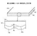
図12は本発明の実施例7になるタッチパネル用保護シート100を示す。保護シート100は透明であるPETフィルム本体101の裏面にストライプ状の微粘着層部102を有する構成である。微粘着層部102は梨地パターンで表してあり、PETフィルム本体101に部分的に設けてある。以下の図面においても、微粘着層部102は梨地パターンで表す。 FIG. 12 shows a touch panel
微粘着層部102がストライプ状であるため、保護シート100をタッチパネル50上に貼り付けるときに、微粘着層部がPETフィルム本体101の全面に形成されている構成に比較して、気泡の発生及び異物の巻き込みは起き難い。 Since the slightly
保護シート100のタッチパネル50上への貼り付けを保護シート100の一端側からストライプの長手方向に進めることによって、貼り付けは円滑に行われる。また、微粘着層部102がストライプ状であるため、貼り付けた保護シート100を部分的に剥離することも容易である。 By affixing the
また、PETフィルム本体101は、図13に示すように、粗さRaが50μm程度の粗い裏面101aを有している。これにより、保護シート100をタッチパネル50上に貼り付けた状態において、タッチパネル50の表面とPETフィルム本体101の裏面101aとの間の隙間が不均一となって、目障りとなるニュートンリングが現れることが防止される。 Further, as shown in FIG. 13, the PET film
なお、PETフィルム本体101の表面にハードコート層114を有していてもよい。 Note that a
図14は本発明の実施例8になるタッチパネル用保護シート110を示す。保護シート110は透明であるPETフィルム本体111の裏面に格子状の微粘着層部112を有する構成である。 FIG. 14 shows a touch panel
微粘着層部112が格子状であるため、保護シート100をタッチパネル50上に貼り付けるときに、貼り付けを格子単位で行うことが可能であり、気泡の発生及び異物の巻き込みは起き難い。また貼り付けた保護シート110を格子単位で剥離することが可能である。Since the slightly
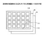
図15(A)は本発明の実施例9になるタッチパネル用保護シート120を示す。保護シート120は、透明であるPETフィルム本体121の裏面に微粘着層部122を有する構成である。この保護シート120は、図15(B)に示すように、液晶パネル70とこの上面側のタッチパネル50とよりなる構造のPDA72の表示・入力部73の上面に、即ち、タッチパネル50の上面に接着されて取り付けられる。 FIG. 15A shows a touch panel
液晶パネル70の破線で囲む部分は、PDA72の電源をオンとしたときに表示される画像キー130〜135である。画像キー130〜134は使用頻度の高いキーである。画像キー135はシステムダウンキーであり、誤った入力操作が不都合を招くキーである。A portion surrounded by abroken line of the
微粘着層部122は、画像キー130〜134に対応する部分を除いた部分に形成してある。即ち、微粘着層部122は、PETフィルム本体121の周囲の部分と、隣り合う画像キー130〜134の境の部分と、且つ、画像キー135に対応する部分に形成してある。122aはPETフィルム本体121の周囲の部分の微粘着層部分、122bは隣り合う画像キー130〜134の境の部分の微粘着層部分、122cは画像キー135に対応する部分の微粘着層部分である。 The slightly
図15(B)は保護シート120が貼られて取り付けられた状態を示す。微粘着層部122が形成してある部分が部分的であるため、保護シート120をタッチパネル50上に貼り付けるときに、気泡の発生及び異物の巻き込みは起き難い。 FIG. 15B shows a state where the
PDAの電源がオンとされた使用状態において、保護シート120及びタッチパネル50を通して液晶パネル70の画像キー130〜135を見ることが可能であり、保護シート120の上面から画像キー130〜135が押し付け操作される。 When the PDA is turned on, the
画像キー130〜134の部分については、PETフィルム本体121とタッチパネル50とは間に空気層138を介在させて対向している状態となっており、入力するのに必要な入力荷重は10〜100grであり通常である。 Regarding the
しかし、画像キー135の部分については、PETフィルム本体121とタッチパネル50との間が微粘着層部分122cでもって占められている状態となっており、保護シート120は空気層138が介在している部分に比較して撓みにくくなっており、入力荷重は40〜150grと通常よりも高くなっている。よって、画像キー135については無意識に触れた程度では入力されず、意識して押した場合に初めて入力され、誤って、PDAがシステムダウンされる不都合は起き難くなる。 However, the portion of the
ここで、保護シート120のうち微粘着層部122の部分を頻繁に押す操作を行うと微粘着層部がタッチパネル50から剥離して剥離した部分に空気が進入して保護シート120の上面から見た場合に、頻繁に押し操作をした部分が白濁してくる場合がある。しかし、上記の保護シート120は頻繁に押す操作が繰り返される画像キー130〜134の部分については微粘着層部が存在しないため、上記の白濁するという不都合は起きない。また、画像キー135は頻繁には押されないキーであるので、微粘着層部分122cが存在しても、上記の白濁には到らない。 Here, when the operation of frequently pressing the portion of the slightly
なお、保護シート120は、画像キー135に対応する微粘着層部分122cを無くして、全ての画像キー130〜135の部分を微粘着層部分が存在しない構造とすることも出来、或いは、逆に全ての画像キー130〜135の部分に微粘着層部分が存在する構造とすることも出来る。 The
また、保護シート120が貼られた状態でタッチパネル50の完成品とすることも出来る。 Moreover, it can also be set as the finished product of the
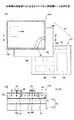
図16(A)、(B)は本発明の実施例10になるタッチパネル用保護シート140を示す。保護シート140は、透明であるPETフィルム本体141の表面にハードコート142を有し、PETフィルム本体141の裏面の全面にドットスペーサ144を有し、且つ、PETフィルム本体141の裏面の周囲に微粘着層部143を有する構成である。この保護シート140は、その周囲の部分を、液晶パネル70とこの上面側のタッチパネル50とよりなる構造のPDA72の表示・入力部73の上面に、即ち、タッチパネル50の上面に接着されて取り付けられる。液晶パネル70は図15(A)に示すと同様に画像キー130〜135を表示する。Figure 16(A), (B) shows a touch panel
ドットスペーサ144は、標準の高さh2を有し、標準のピッチp2で分散して配置してある。但し、PETフィルム本体141の裏面のうち画像キー135に対応する領域145については、ドットスペーサ144は、上記のピッチp2よりも広いピッチp3でもって、配置してある。 The dot spacers 144 have a standard height h2 and are distributed at a standard pitch p2. However, in the
図17(A),(B)に示すように、保護シート140が押されて撓まされたときに、ドットスペーサ144がタッチパネル50の上側のフィルム60の上面を押し、フィルム60を撓ませる。よって、ドットスペーサ144付きの保護シート140を設けることによって、保護シートを設けない場合に比較して、入力荷重が軽減される。As shown in FIGS. 17A and 17B, when the
ここで、ドットスペーサ144のピッチと入力荷重との関係について説明する。図18に示すように、ドットスペーサ144のピッチが狭いと、入力荷重が増加し、ドットスペーサ144のピッチを広くすると、入力荷重が低くなる。Here, the relationship between the pitch of the
よって、画像キー130〜134の部分については、ドットスペーサ144がピッチp3で分散して配置してあるため、入力荷重は10〜100grであり略通常である。Therefore, the portion of the image key 130-134, since the
しかし、画像キー135の部分については、ドットスペーサ144がピッチp2で分散して配置してあるため、入力荷重は40〜150grと通常よりも高くなっている。よって、画像キー135については無意識に触れた程度では入力されず、意識して押した場合に初めて入力され、誤って、PDAがシステムダウンされる不都合は起き難くなる。However, the portion of the
なお、保護シート140のうち画像キー130〜134に対向する部分についても、使用頻度等に応じてドットスペーサ144のピッチを変えてもよい。 Note that the pitch of the
図19(A)、(B)は本発明の実施例11になるタッチパネル用保護シート150を示す。保護シート150は、透明であるPETフィルム本体151の表面にハードコート152を有し、PETフィルム本体151の裏面の全面にドットスペーサ154a,ドットスペーサ154bを有し、且つ、PETフィルム本体151の裏面の周囲に微粘着層部153を有する構成である。この保護シート150は、その周囲の部分を、液晶パネル70とこの上面側のタッチパネル50とよりなる構造のPDAの表示・入力部73の上面に、即ち、タッチパネル50の上面に接着されて取り付けられる。液晶パネル70は図15(A)に示すと同様に画像キー130〜135を表示する。Figure 19(A), (B) shows a touch panel
ドットスペーサ154aは、標準のスペーサ高さh2を有し、標準のピッチp2で分散して配置してある。但し、PETフィルム本体151の裏面のうち画像キー135に対応する領域155については、高さh2よりも低い高さh3を有するドットスペーサ154bが標準のピッチp2で配置してある。The
ここで、ドットスペーサの高さと入力荷重との関係について説明する。図20に示すように、ドットスペーサのピッチが一定である条件で、ドットスペーサの高さが高いと、入力荷重が低下し、ドットスペーサの高さが低いと、入力荷重が高くなる。 Here, the relationship between the height of the dot spacer and the input load will be described. As shown in FIG. 20, when the dot spacer pitch is constant and the dot spacer pitch is high, the input load decreases, and when the dot spacer height is low, the input load increases.
よって、画像キー130〜134の部分については、高さがh2であるドットスペーサ154aが分散して配置してあるため、入力荷重は10〜100grであり略通常である。 Therefore, since the
しかし、画像キー135の部分については、高さがh2よりも低いh3であるドットスペーサ154bが分散して配置してあるため、入力荷重は40〜150grと通常よりも高くなっている。よって、画像キー135については無意識に触れた程度では入力されず、意識して押した場合に初めて入力され、誤って、PDA72がシステムダウンされる不都合は起き難くなる。However, since the
なお、保護シート140のうち画像キー130〜134に対向する部分についても、使用頻度等に応じて高さの異なるドットスペーサを設けてもよい。
変えてもよい。In addition, dot spacers having different heights may be provided on portions of the
You may change it.
図21は本発明の実施例12になるタッチパネル用保護シート160を示す。保護シート160は、透明であるPETフィルム本体161の表面にハードコート162を有し、PETフィルム本体161の裏面の全面にドットスペーサを高さとピッチとの両方を変えて配置してあり、且つ、PETフィルム本体161の下面の周囲に微粘着層部163を有する構成である。 FIG. 21 shows a touch panel
領域200については、高さがh2のドットスペーサ154aが標準のピッチp2で分散してあり、領域201については、高さがh3のドットスペーサ154bがピッチp3で分散してあり、領域202については、高さがh1のドットスペーサ154cがピッチp1で分散してある。領域201は入力荷重が通常よりも高くなり、領域202は入力荷重が通常よりも低くなる。領域202を頻繁に入力操作を行う画像キーに対応する部分に配置することによって、操作者は疲れにくくなり、PDAは操作性が向上する。For the
50、50A〜50E タッチパネル
51 ガラス板
52 透明導電膜(ITO膜)
59 両面接着テープ
60、60A〜60E フィルム
61、61B PETフィルム本体
61C 耐熱PETフィルム本体
62 透明導電膜(ITO膜)
63、81、91 耐熱アクリル系樹脂の層
72 PDA
100、110、120、140、150、160 タッチパネル用保護シート
102,112,122c,143,153,163 微粘着層部
144、154a,154b ドットスペーサ50, 50A-
59 Double-sided
63, 81, 91 Heat-resistant
100, 110, 120, 140, 150, 160 Protective sheet for
Claims (2)
Translated fromJapanese該フィルムは、該フィルム本体の表面に、耐熱アクリル系樹脂製の表面層を有し、該フィルム本体の裏面側については、耐熱アクリル系樹脂製の裏面層を有し、該裏面層の下面に前記透明導電膜を有することを特徴とするタッチパネル。In the touch panel provided with a film having a transparent conductive film onthe back surface of thefilm body and operated by being pressed or rubbed with a pen on the surface side,
The film hasa surface layer made of a heat-resistant acrylic resin on the surface of the film body, and the back side of the film body has a back layer made of a heat-resistant acrylic resin, on the lower surface of the back layer. A touch panelcomprising the transparent conductive film .
フィルム本体の表面に、耐熱アクリル系樹脂製の表面層を有し、該フィルム本体の裏面側に、耐熱アクリル系樹脂製の裏面層を有し、且つ、該裏面層の下面に前記透明導電膜を有することを特徴とするタッチパネル用フィルム。The surface of the film body has a surface layer made of a heat-resistant acrylic resin, the back surface side of the film body has a back layer made of heat-resistant acrylic resin, and the transparent conductive film on the lower surface of the back surface layer A film for a touch panel comprising:
Priority Applications (3)
| Application Number | Priority Date | Filing Date | Title |
|---|---|---|---|
| JP2004096230AJP4336232B2 (en) | 2004-03-29 | 2004-03-29 | Touch panel |
| US10/870,029US7432913B2 (en) | 2004-03-29 | 2004-06-18 | Touch panel, film therefor, and protection sheet therefor that can extend the life cycle of the touch panel |
| US12/199,384US7636084B2 (en) | 2004-03-29 | 2008-08-27 | Touch panel, film therefor, and protection sheet therefor that can extend the life cycle of the touch panel |
Applications Claiming Priority (1)
| Application Number | Priority Date | Filing Date | Title |
|---|---|---|---|
| JP2004096230AJP4336232B2 (en) | 2004-03-29 | 2004-03-29 | Touch panel |
Related Child Applications (1)
| Application Number | Title | Priority Date | Filing Date |
|---|---|---|---|
| JP2009066168ADivisionJP4768041B2 (en) | 2009-03-18 | 2009-03-18 | Protective sheet for touch panel |
Publications (3)
| Publication Number | Publication Date |
|---|---|
| JP2005284603A JP2005284603A (en) | 2005-10-13 |
| JP2005284603A5 JP2005284603A5 (en) | 2009-02-05 |
| JP4336232B2true JP4336232B2 (en) | 2009-09-30 |
Family
ID=34989213
Family Applications (1)
| Application Number | Title | Priority Date | Filing Date |
|---|---|---|---|
| JP2004096230AExpired - Fee RelatedJP4336232B2 (en) | 2004-03-29 | 2004-03-29 | Touch panel |
Country Status (2)
| Country | Link |
|---|---|
| US (2) | US7432913B2 (en) |
| JP (1) | JP4336232B2 (en) |
Families Citing this family (19)
| Publication number | Priority date | Publication date | Assignee | Title |
|---|---|---|---|---|
| US7609512B2 (en)* | 2001-11-19 | 2009-10-27 | Otter Products, Llc | Protective enclosure for electronic device |
| KR20070047668A (en)* | 2005-11-02 | 2007-05-07 | 삼성에스디아이 주식회사 | Flat panel display for reducing the temperature difference |
| US20080107830A1 (en)* | 2006-11-03 | 2008-05-08 | Motorola, Inc. | Image-providing apparatus and method for communication device |
| KR101356777B1 (en)* | 2006-12-13 | 2014-01-27 | 삼성디스플레이 주식회사 | Touch screen panel |
| KR100984071B1 (en)* | 2007-03-30 | 2010-09-30 | 후지쯔 콤포넌트 가부시끼가이샤 | Touch panel |
| JP4993613B2 (en)* | 2008-02-29 | 2012-08-08 | 株式会社ジャパンディスプレイイースト | Manufacturing method of display device |
| US20100052879A1 (en)* | 2008-08-29 | 2010-03-04 | Nanos Steven G | Apparatus and Method for the Tactile Identification of Keys and Regions of a Touch-Responsive Device |
| KR101007471B1 (en) | 2008-10-08 | 2011-01-12 | 이한준 | Method for manufacturing protective cover glass substrate by joining two glass substrates and using the protective cover glass substrate applied to flat panel display |
| KR101558915B1 (en)* | 2009-03-27 | 2015-10-13 | 삼성디스플레이 주식회사 | Touch screen module with protective window |
| US20110088844A1 (en)* | 2009-10-16 | 2011-04-21 | Apple Inc. | Thermally activated adhesive and fixture for improving registration accuracy between assembled parts |
| US20110147438A1 (en)* | 2009-12-23 | 2011-06-23 | Carl Ludwig Deppisch | Clad solder thermal interface material |
| KR101643377B1 (en)* | 2010-02-26 | 2016-07-28 | 삼성전자주식회사 | Foldable touch screen display apparatus |
| JP5758881B2 (en)* | 2010-03-29 | 2015-08-05 | 株式会社きもと | Newton ring prevention sheet, manufacturing method thereof, and touch panel |
| WO2011138200A1 (en)* | 2010-05-06 | 2011-11-10 | Iee International Electronics & Engineering S.A. | Input device |
| LU91702B1 (en)* | 2010-06-21 | 2011-12-22 | Iee Sarl | Input device |
| KR101119355B1 (en)* | 2010-09-09 | 2012-03-07 | 삼성전기주식회사 | Touch panel |
| JP2013065117A (en)* | 2011-09-15 | 2013-04-11 | Fujitsu Component Ltd | Touch panel |
| JP5534619B2 (en)* | 2012-10-18 | 2014-07-02 | 任天堂株式会社 | Protective sheet mounting structure |
| KR20170101881A (en)* | 2014-12-17 | 2017-09-06 | 미쯔비시 케미컬 주식회사 | Image display apparatus provided with touch panel |
Family Cites Families (16)
| Publication number | Priority date | Publication date | Assignee | Title |
|---|---|---|---|---|
| JPS61237313A (en) | 1985-04-12 | 1986-10-22 | シャープ株式会社 | thin film touch panel |
| JPH03216718A (en) | 1990-01-22 | 1991-09-24 | Toray Ind Inc | Pressure sensitive input tablet |
| JPH0931421A (en) | 1995-07-20 | 1997-02-04 | Mitsubishi Electric Corp | Surface protection sheet |
| JP3426847B2 (en) | 1996-05-14 | 2003-07-14 | アルプス電気株式会社 | Coordinate input device |
| JPH09235525A (en) | 1996-02-29 | 1997-09-09 | Sumiron:Kk | Film roll for coating film protection |
| KR100630147B1 (en)* | 1998-09-10 | 2006-10-02 | 군제 가부시키가이샤 | Touch panel |
| JP2001060144A (en) | 1999-08-24 | 2001-03-06 | Nissha Printing Co Ltd | High durability input device |
| JP2002197924A (en) | 2000-12-26 | 2002-07-12 | Bridgestone Corp | Transparent conductive film, method for producing the same, and touch panel |
| WO2003014202A1 (en)* | 2001-08-07 | 2003-02-20 | Teijin Dupont Films Japan Limited | Biaxially oriented layered polyester film and film with hard coat layer |
| JP2003157149A (en) | 2001-09-06 | 2003-05-30 | Nissha Printing Co Ltd | Touch panel having high durability |
| WO2003023594A1 (en)* | 2001-09-06 | 2003-03-20 | Nissha Printing Co., Ltd. | Touch panel having high durability |
| CN1321971C (en)* | 2001-10-10 | 2007-06-20 | Jsr株式会社 | Norbornene derivative and norbornene polymer obtained therefrom through ring opening polymerization |
| KR100479474B1 (en)* | 2001-12-26 | 2005-03-30 | 엘지.필립스 엘시디 주식회사 | Touch Panel and Fabricated Method of Dot Spacer Thereof |
| KR101082239B1 (en)* | 2002-11-11 | 2011-11-09 | 미츠비시 레이온 가부시키가이샤 | Acrylic Resin Resin Boards Transparent Electrode Boards for Touch Panels Touch Panels and Processes for Production of Them |
| JP2004259256A (en)* | 2003-02-05 | 2004-09-16 | Nitto Denko Corp | Transparent laminate, pen input image display device, and image display method |
| US7289111B2 (en)* | 2004-03-25 | 2007-10-30 | International Business Machines Corporation | Resistive touch pad with multiple regions of sensitivity |
- 2004
- 2004-03-29JPJP2004096230Apatent/JP4336232B2/ennot_activeExpired - Fee Related
- 2004-06-18USUS10/870,029patent/US7432913B2/ennot_activeExpired - Fee Related
- 2008
- 2008-08-27USUS12/199,384patent/US7636084B2/ennot_activeExpired - Fee Related
Also Published As
| Publication number | Publication date |
|---|---|
| US7636084B2 (en) | 2009-12-22 |
| JP2005284603A (en) | 2005-10-13 |
| US20050212776A1 (en) | 2005-09-29 |
| US7432913B2 (en) | 2008-10-07 |
| US20080309642A1 (en) | 2008-12-18 |
Similar Documents
| Publication | Publication Date | Title |
|---|---|---|
| JP4336232B2 (en) | Touch panel | |
| JP7079767B2 (en) | Keyboard with adaptive input sequence | |
| KR100893498B1 (en) | Touch panel | |
| EP2703963B1 (en) | Spacer-less input device | |
| EP2573660B1 (en) | Touch panel and portable device using the same | |
| US20040125086A1 (en) | Touch input device having removable overlay | |
| US20110012842A1 (en) | Touch panel using tempered glass | |
| US20110304579A1 (en) | Touch panel | |
| TWI361997B (en) | ||
| JP2005530996A (en) | Touch sensor | |
| JP2011048541A (en) | Touch panel-equipped display device | |
| CN101587401B (en) | Touch Panel and Display Device | |
| JP2004070802A (en) | Transparent touch panel | |
| JP4768041B2 (en) | Protective sheet for touch panel | |
| CN102667694A (en) | Input device, display device, and portable terminal | |
| KR101084802B1 (en) | Touch screen device | |
| US20110242011A1 (en) | Touch input device | |
| KR100896458B1 (en) | Touch panel | |
| CN105929580A (en) | Resistive touch display device | |
| EP2169520A2 (en) | Touch panel using tempered glass | |
| KR100893499B1 (en) | Touch panel | |
| JP2012048274A (en) | Input device and display having the same | |
| JP2012248010A (en) | Input device, display apparatus, and equipment | |
| US20130134025A1 (en) | Resistive touch display panel having anti-scrape layer | |
| US20110291957A1 (en) | Touch-type transparent keyboard |
Legal Events
| Date | Code | Title | Description |
|---|---|---|---|
| A621 | Written request for application examination | Free format text:JAPANESE INTERMEDIATE CODE: A621 Effective date:20070112 | |
| A521 | Request for written amendment filed | Free format text:JAPANESE INTERMEDIATE CODE: A523 Effective date:20081212 | |
| A131 | Notification of reasons for refusal | Free format text:JAPANESE INTERMEDIATE CODE: A131 Effective date:20090120 | |
| A521 | Request for written amendment filed | Free format text:JAPANESE INTERMEDIATE CODE: A523 Effective date:20090318 | |
| TRDD | Decision of grant or rejection written | ||
| A01 | Written decision to grant a patent or to grant a registration (utility model) | Free format text:JAPANESE INTERMEDIATE CODE: A01 Effective date:20090623 | |
| A01 | Written decision to grant a patent or to grant a registration (utility model) | Free format text:JAPANESE INTERMEDIATE CODE: A01 | |
| A61 | First payment of annual fees (during grant procedure) | Free format text:JAPANESE INTERMEDIATE CODE: A61 Effective date:20090626 | |
| FPAY | Renewal fee payment (event date is renewal date of database) | Free format text:PAYMENT UNTIL: 20120703 Year of fee payment:3 | |
| R150 | Certificate of patent or registration of utility model | Free format text:JAPANESE INTERMEDIATE CODE: R150 | |
| FPAY | Renewal fee payment (event date is renewal date of database) | Free format text:PAYMENT UNTIL: 20120703 Year of fee payment:3 | |
| FPAY | Renewal fee payment (event date is renewal date of database) | Free format text:PAYMENT UNTIL: 20130703 Year of fee payment:4 | |
| R250 | Receipt of annual fees | Free format text:JAPANESE INTERMEDIATE CODE: R250 | |
| R250 | Receipt of annual fees | Free format text:JAPANESE INTERMEDIATE CODE: R250 | |
| S531 | Written request for registration of change of domicile | Free format text:JAPANESE INTERMEDIATE CODE: R313531 | |
| R350 | Written notification of registration of transfer | Free format text:JAPANESE INTERMEDIATE CODE: R350 | |
| R250 | Receipt of annual fees | Free format text:JAPANESE INTERMEDIATE CODE: R250 | |
| R250 | Receipt of annual fees | Free format text:JAPANESE INTERMEDIATE CODE: R250 | |
| LAPS | Cancellation because of no payment of annual fees |