JP4332174B2 - Input device and manufacturing method thereof - Google Patents
Input device and manufacturing method thereofDownload PDFInfo
- Publication number
- JP4332174B2 JP4332174B2JP2006325611AJP2006325611AJP4332174B2JP 4332174 B2JP4332174 B2JP 4332174B2JP 2006325611 AJP2006325611 AJP 2006325611AJP 2006325611 AJP2006325611 AJP 2006325611AJP 4332174 B2JP4332174 B2JP 4332174B2
- Authority
- JP
- Japan
- Prior art keywords
- conductive film
- base material
- conductive
- input device
- wiring
- Prior art date
- Legal status (The legal status is an assumption and is not a legal conclusion. Google has not performed a legal analysis and makes no representation as to the accuracy of the status listed.)
- Expired - Fee Related
Links
Images


Classifications
- G—PHYSICS
- G06—COMPUTING OR CALCULATING; COUNTING
- G06F—ELECTRIC DIGITAL DATA PROCESSING
- G06F3/00—Input arrangements for transferring data to be processed into a form capable of being handled by the computer; Output arrangements for transferring data from processing unit to output unit, e.g. interface arrangements
- G06F3/01—Input arrangements or combined input and output arrangements for interaction between user and computer
- G06F3/03—Arrangements for converting the position or the displacement of a member into a coded form
- G06F3/041—Digitisers, e.g. for touch screens or touch pads, characterised by the transducing means
- G06F3/044—Digitisers, e.g. for touch screens or touch pads, characterised by the transducing means by capacitive means
- G06F3/0445—Digitisers, e.g. for touch screens or touch pads, characterised by the transducing means by capacitive means using two or more layers of sensing electrodes, e.g. using two layers of electrodes separated by a dielectric layer
Landscapes
- Engineering & Computer Science (AREA)
- General Engineering & Computer Science (AREA)
- Theoretical Computer Science (AREA)
- Human Computer Interaction (AREA)
- Physics & Mathematics (AREA)
- General Physics & Mathematics (AREA)
- Position Input By Displaying (AREA)
Description
Translated fromJapanese本発明は、指などの操作体が接触あるいは接近したこと平面電極を用いて検出する静電式の入力装置の製造方法に係わり、特に、機器内部から発生する輻射ノイズの影響を押さえるシールド層を有する入力装置及びその製造方法に関する。 The present invention relates to a method for manufacturing an electrostatic input device that detects that an operating body such as a finger is in contact or approached by using a planar electrode, and in particular, a shield layer that suppresses the influence of radiation noise generated from inside the device. It is related with the input device which has, and its manufacturing method.
以下に示す特許文献には透明な容量検出型のセンサに関する発明が開示されている。例えば特許文献1の図6に示すように、センサは透明な絶縁体の表面に積層された透明なX導体トレースと裏面に積層されたY導体トレースとを有して構成されている。さらに、センサの下層側には均一層からなる透明な導体が設けられている。このセンサでは前記導体を接地することにより、下部側の位置に設けられた電気回路(例えば、表示装置など)から生じる電気ノイズ源から前記センサを隔離できるようになっている。
一般に電子機器では電圧や電流を変化させて信号を伝送する。電圧や電流を変化させた場合、ラインからの電磁波(輻射ノイズ)が発生する。この輻射ノイズが強いと近くのセンサに悪影響を与えるため、センサの精度を低下させる。したがって、センサと電気回路との間に接地された透明な導体からなるシールド層を配置することは、輻射ノイズの影響がセンサに及ばないようにするための手段としては有効である。 In general, electronic devices transmit signals by changing voltage or current. When voltage or current is changed, electromagnetic waves (radiation noise) from the line are generated. If this radiation noise is strong, it will adversely affect nearby sensors, reducing the accuracy of the sensor. Therefore, disposing a shield layer made of a transparent conductor grounded between the sensor and the electric circuit is effective as a means for preventing the influence of radiation noise from affecting the sensor.
しかし、特許文献1に示すセンサは、前記X、Yの導体トレースがそれぞれ別個に用意された透明な基板の上に形成した後、間に絶縁体を介在させた状態で両基板を両側から貼り合わせることにより製造されるため、製造コストの高騰を抑え難いという問題がある。 However, in the sensor disclosed in
本発明は上記従来の課題を解決するためのものであり、輻射ノイズの影響を抑えるシールド層を備える安価な静電式の入力装置及びその製造方法を提供することを目的としている。 The present invention has been made to solve the above-described conventional problems, and an object thereof is to provide an inexpensive electrostatic input device including a shield layer that suppresses the influence of radiation noise and a method for manufacturing the same.
また本発明はXY型とは異なる平面電極を用いた静電式の入力装置においては、平面電極と対向配置されたシールド電極自体の電位がふら付くと、検出値が不安定になりやすいという問題もある。 Further, in the electrostatic input device using the planar electrode different from the XY type according to the present invention, if the potential of the shield electrode itself arranged opposite to the planar electrode fluctuates, the detection value tends to become unstable. There is also.
本発明は、平面電極を用いた静電式の入力装置において、安定して動作する入力装置及びその製造方法を提供することを目的としている。 An object of the present invention is to provide an input device that operates stably in an electrostatic input device using planar electrodes, and a method for manufacturing the same.
本発明は、操作体との間での静電容量変化を検出するセンサ部を有する入力装置において、
透明な基材の表裏両面に導電膜が夫々設けられ、
前記基材の表面には、前記導電膜が区画溝によって所定形状に分離されることにより前記センサ部を構成する複数の電極部及び配線導電膜が形成されており、
前記基材の裏面には、前記表面に形成された前記複数の電極部を重ねたときに、同一の形状及び配列で重なり合う複数の電極部及び前記基材の周辺部以外の位置に配置された前記電極部から前記周辺部へ延びる複数の配線導電膜と、前記周辺部に枠状に形成された導通パターンとが設けられ、
前記基材の両面に形成された複数の電極部及び複数の配線導電膜は、前記基材の一方の面から照射されて他方の面に抜けるレーザ光によって前記基材の表裏両面に設けられた導電膜に同時に形成される前記区画溝により分離されたものであり、
前記周辺部に設けられた前記複数の電極部と前記複数の配線導電膜とが前記導通パターンを介して導通接続されて、前記基材の裏面に形成されている全ての前記電極部が同電位に設定されていることを特徴とするものである。The present invention provides an input device having a sensor unit that detects a change in capacitance with an operating body.
Conductive films are provided on both sides of thetransparent base material,
On the surface of the base material, the conductive film is separated into a predetermined shape by a partition groove,and a plurality of electrode partsand a wiring conductive film that form the sensor partare formed ,
On the back surface of thebase material , when the plurality of electrode portions formed on the front surface are overlapped, theyare arranged at positions other than the plurality of electrode portions overlapping in the same shape and arrangement andthe peripheral portion of the base material. A plurality of wiring conductive films extending from the electrode part to the peripheral part, and a conductive pattern formed in a frame shape on the peripheral part are provided,
The plurality of electrode portions and the plurality of wiring conductive films formed on both surfaces of the base material are provided on both front and back surfaces of the base material by laser light that is irradiated from one surface of the base material and exits to the other surface. Separated by the partition grooves formed simultaneously in the conductive film,
The plurality of electrode portions provided in the peripheral portion and the plurality of wiring conductive films are conductively connected through the conductive pattern, and all the electrode portions formed on the back surface of the base material have the same potential. It is characterizedby being set to .
本発明の入力装置では、基材の表面に配置される電極部と基材の裏面に配置される電極部とを同一形状、同一配列とすることができる。このため、各電極部によって形成される各センサ部の静電容量Cが一定以上とすることができ、安定性の良いタッチセンサとすることができる。 In the input device of the present invention, the electrode portions arranged on the surface of the substrate and the electrode portions arranged on the back surface of the substrate can have the same shape and the same arrangement. For this reason, the electrostatic capacitance C of each sensor part formed by each electrode part can be set to a certain level or more, and a touch sensor with good stability can be obtained.
また本発明は、操作体との間での静電容量変化を検出するセンサ部を有する入力装置の製造方法において、
(a)透明な基材の両面に導電膜を形成する工程、
(b) レーザ光を一方の導電膜に向けて照射して前記両面の導電膜に対して同時に区画溝を形成し、複数の所定形状の区画からなる前記センサ部を構成する電極部と配線導電膜を形成する工程、
(c) 前記一方の導電膜に形成された一部の前記配線導電膜上に絶縁層を形成する工程、
(d) 絶縁層上に、前記個々の電極部の夫々に対して電気的に接続される配線パターンを形成する工程、
(e) 他方の導電膜に、前記区画溝により分離された個々の電極部間を導通接続する導通パターンを形成する工程、
の順で行われることを特徴とするものである。Further, the present invention provides a method for manufacturing an input device having a sensor unit that detects a change in capacitance with an operating body.
(A) forming a conductive film on both surfaces of atransparent substrate;
(B) A laser beam is irradiated towardone of the conductive films to form partition groovessimultaneously on the conductive films on both sides, and the electrode section and the wiring conductor constituting the sensor section composed of a plurality of sections having a predetermined shape a process thatform the membrane,
(C) forming an insulating layer on a part of the wiring conductive film formed on the one conductive film;
(D) forming a wiring pattern electrically connected to each of the individual electrode portions on the insulating layer;
(E) forming a conductive pattern for conductively connecting the individual electrode parts separated by the partitioning groove on the other conductive film;
It is characterizedby beingperformed in the order of .
本発明では、製造工程の一部を省略化ないしは簡略化することができるため、製造コストの高騰を抑えることができる。 In the present invention, since a part of the manufacturing process can be omitted or simplified, an increase in manufacturing cost can be suppressed.
上記においては、前記(e)工程の後に、
(f) 前記一方の導電膜を透明な絶縁層で覆う工程、
(g) 前記他方の導電膜を透明な絶縁層で覆う工程、
を有するものが好ましい。In the above,after the step (e),
(F) step of covering with a transparent insulating layerprior SL one conductive film,
(G) covering the other conductive film with a transparent insulating layer;
Those having the following are preferred.
上記において、例えば、
前記(c)の工程の後に前記(e)の工程が行われ、その後に前記(d)の工程が行われるものとすることができる。In the above, for example,
The step (e) is performed after the step (c), and then the step (d) is performed.
あるいは、前記(b)の工程の後に前記(e)の工程が行われ、その後に前記(c)の工程、前記(d)の工程が行われるものとすることもできる。 Alternatively, the step (e) may be performed after the step (b), and then the step (c) and the step (d) may be performed.
本発明では、誤動作が少なく、安定して動作する静電式の入力装置とすることができる。 In the present invention, it is possible to provide an electrostatic input device that operates stably with few malfunctions.
また本発明では、製造に要する時間を短縮化することができるとともに、製造工程を簡略化することができるため、製造コストの高騰を抑えることが可能となる。 In addition, according to the present invention, it is possible to shorten the time required for manufacturing and simplify the manufacturing process, thereby suppressing an increase in manufacturing cost.
図1は本発明の実施の形態としてのタッチセンサ(平面電極を用いた静電式の入力装置)を示す平面図であり、図1Aは表面を示す平面図、図1Bは裏面を示す背面図、図2は第1の実施の形態としての入力装置の一部を拡大して示す部分断面図である。なお、各図におけるX方向は横方向、Y方向は縦方向、Z方向は膜厚方向(Z)を示し、各方向は残り2つの方向に対し直交関係にある。前記膜厚方向(Z)のうち、Z1方向は指やペンなどの操作体が位置する上方を示しており、Z2方向は液晶表示装置20などが配置される下方を示している。 FIG. 1 is a plan view showing a touch sensor (an electrostatic input device using planar electrodes) as an embodiment of the present invention, FIG. 1A is a plan view showing a front surface, and FIG. 1B is a rear view showing a back surface. FIG. 2 is an enlarged partial cross-sectional view showing a part of the input device as the first embodiment. In each figure, the X direction is the horizontal direction, the Y direction is the vertical direction, the Z direction is the film thickness direction (Z), and each direction is orthogonal to the remaining two directions. Among the film thickness directions (Z), the Z1 direction indicates the upper side where an operating body such as a finger or a pen is positioned, and the Z2 direction indicates the lower side where the liquid
本実施形態におけるタッチセンサ(平面電極を用いた静電式の入力装置)TSは、液晶などの表示装置の上に積層された状態で、例えば携帯電話機、PDAなどからなる電子機器に搭載される。タッチセンサは、人の指やペンなどの操作体が指し示した前記表示装置上の座標位置を検出し、この入力情報を電子機器内の制御部に与える機能を有するものである。 The touch sensor (electrostatic input device using a planar electrode) TS in the present embodiment is mounted on an electronic device such as a mobile phone or a PDA in a state of being stacked on a display device such as a liquid crystal. . The touch sensor has a function of detecting a coordinate position on the display device indicated by an operation body such as a human finger or a pen, and providing the input information to a control unit in the electronic device.
図1A、図1Bおよび図2に示すように、本実施形態におけるタッチセンサTSは、基材1、導電膜2A,2B、絶縁層6、配線パターン7、さらにはフレキシブルケーブル12などを有して構成される。 As shown in FIG. 1A, FIG. 1B, and FIG. 2, the touch sensor TS in this embodiment includes a
基材1は、例えばポリエチレンテレフタレート(PET)など透明性および絶縁性を有するシート状の部材で形成される。また基材1は可撓性であることが好ましい。前記基材1が可撓性を有する場合には、タッチセンサTSを曲面の筐体に取り付けることができる等、取り付けの自由度を向上させる上で好適である。The
前記導電膜2Aは透明な基材1の上面に対し、例えばITOなどからなる透明な薄い金属膜として形成されている。前記導電膜2Aには、例えば図1Aに示すように、縦方向及び横方向を長手方向とする複数の区画溝3と、前記複数の区画溝3により分離され且つマトリックス状に配列された複数の電極部4(個別に、4a〜4oで示す)と、前記電極部4a〜4o以外の部分で且つ区画溝3内に形成された配線導電膜5などが設けられている。個々の電極部4a〜4oは、所定の面積を有する略長方形からなる透明電極で形成され、それぞれセンサ部として機能している。なお、各電極部4a〜4oはある程度の面積を有していればよく、電極部4a〜4oがすべて同じ形状および同じ面積で構成されていなくてもよい。The
X1方向の端部およびX2方向の端部では、隣り合う電極部4どうしの間、すなわち区画溝3や配線導電膜5の上部に絶縁層6が部分的に積層されている。そして、この絶縁層6の上には複数の配線パターン7が形成されている。個々の配線パターン7の一端7aは前記電極部4a〜4oのいずれかに夫々接続されており、他端は基材1に接続されたフレキシブルケーブル12を介してタッチセンサTSの外部に引き出されている。そして、これら導電膜2A、絶縁層6および配線パターン7の上、すなわち最上層は透明レジスト材などからなる保護層9で覆われている。 At the end portion in the X1 direction and the end portion in the X2 direction, the insulating
この実施の形態では、基材1の下面側には上記導電膜2A同様の構成からなる導電膜2Bが設けられている。すなわち導電膜2BはITOなど透明な薄い金属膜で形成されている。前記導電膜2Bには、上記同様の区画溝3、電極部4および配線導電膜5が形成されている。 In this embodiment, a
ただし、図1Bに示すように、基材1の裏面側の4つの周辺部には、導通パターン8が枠状に積層されている。導通パターン8は、前記区画溝3によって分離された各電極部4および各配線導電膜5の間を互いに導通接続しており、導電膜2B全体が等しい電位に設定されている。 However, as shown in FIG. 1B,
本実施の形態において、導電膜2BはグランドGNDを構成しており、液晶表示装置20と導電膜2A側の個々の電極部4a〜4oとの間に介在している。このため,導電膜2Bは液晶表示装置20などからの輻射ノイズがセンサ部に与える影響を小さくするシールド層としての機能を有する。In the present embodiment, the
タッチセンサTSでは、導電膜2Aを形成する個々の各電極部4a〜4oと前記グランドGNDを形成する導電膜2Bとの間に所定の電圧が印加される。このとき、導電膜2A側の各電極部4a〜4oと導電膜2B側のグランドGNDとの間に静電容量Cが夫々形成される。 In the touch sensor TS, a predetermined voltage is applied between each of the
操作体が、前記保護層9の表面のいずれかの位置に接すると、操作体と対向するいずれかの導電膜2A側の電極部4と導電膜2B側のグランドGNDとの間に形成された静電容量Cの容量が変化する。このため、図示しない検出回路を用いて前記静電容量Cの変化を検出することにより、前記操作体の位置(XY平面上の位置)を求めることが可能となっている。 When the operating body is in contact with any position on the surface of the
ところで、この種のタッチセンサTSでは、操作者がタッチセンサTSを備えた電子機器を把持すると、指などの操作体はタッチセンサTSの裏側にも接する。このとき、タッチセンサTSの裏側に位置する操作体と基材1の裏側に位置する導電膜2Bとの間の距離が近いと、操作体と導電膜2Bとの間に不要な静電結合が形成され、前記導電膜2Bの電位(グランドGNDの電位)がふら付きやすくなる。このため、場合によってはタッチセンサTSの検出精度が低下する可能性がある。よって、グランドGNDを構成する導電膜2Bと操作体が触れるタッチセンサTSの裏面との間の距離は離れていること(厚いこと)が好ましい。 By the way, in this type of touch sensor TS, when an operator holds an electronic device including the touch sensor TS, an operation body such as a finger also contacts the back side of the touch sensor TS. At this time, if the distance between the operation body located on the back side of the touch sensor TS and the
そこで、本発明では前記導電膜2Bの表面に、透明レジスト材からなる感度調整層10を設けた構成としている。これにより、操作者がタッチセンサTSを把持したときに、操作体とグランドGNDを構成する導電膜2Bとの間に静電結合が形成され難くなり、前記導電膜2Bの電位を安定させることが可能となる。よって、タッチセンサTSの検出精度を高めることが可能となる。Accordingly, in thepresent invention , the
次に、タッチセンサの製造方法について説明する。
図3Aないし図3Gは本発明の実施の形態としての第1の製造方法を工程別に示すタッチセンサの部分断面図である。Next, a method for manufacturing a touch sensor will be described.
3A to 3G are partial cross-sectional views of the touch sensor showing the first manufacturing method according to the embodiment of the present invention by process.
図3Aに示すように、第1の工程では、例えばPET(ポリエチレンテレフタレート)などからなる基材1を用意し、前記基材1の表裏両面に導電膜2A,2Bを形成する。この導電膜2A,2BはITO(酸化インジウムスズ、Indium TinOxide)である。基材1への導電膜2A,2Bの成膜は、例えば真空蒸着法により酸素雰囲気中でITOを蒸着し、その後、大気中で加熱後酸化する方法でITOフィルムを生成する。または放電ガスとしてのArガス中に、若干のガスを混合してDCグロー放電を起こし、生成しAr+カチオンによるITOターゲットのスパッタリングにより、ITO薄膜を基材1に形成する(スパッタ法)。あるいは、圧力勾配型アーク放電ガンを用いて、ITOの蒸発と蒸気の活性化を同時に行うイオンプレーティング法を用いるものであってもよい。なお、市販されている透明導電性フィルムを購入するものであってもよい。 As shown in FIG. 3A, in the first step, a
図3Bに示すように、第2の工程では前記導電膜2A,2Bに複数の区画溝3を図示しないレーザ装置を用いて形成する。レーザ装置からのレーザ光は、基材1を貫通するように一方の面から他方の面に向けて射出される。本実施の形態では、基材1の上方の位置から、Z1側の前記導電膜2Aに向けて出射される。レーザ光は導電膜2Aを切断した後、基材1を膜厚(Z)方向に通り抜けて裏面に設けられた導電膜2Bを切断する。よって、レーザ光を、前記導電膜2A上を横方向及び縦方向に予めプログラミングされた所定の形状に沿って移動させることにより、図1に示すような複数の区画溝3、電極部4(4a〜4o)および配線導電膜5を表裏両面に同時に形成することができる。すなわち、基材1の表面側の前記導電膜2Aに形成された複数の前記区画溝3、電極部4および配線導電膜5と、基材2の裏面側の前記導電膜2Bに形成された複数の前記区画溝3、電極部4および配線導電膜5とは同一形状および同一配列であり、両導電膜2A,2Bに形成された形状は板厚方向において互いに重なり合う。このように、本発明では、膜厚(Z)方向において重なり合う個々の電極部4が互いに同じ形状および同じ配列であるため、導電膜2Aと導電膜2Bとの間に形成される個々の静電容量Cのすべてを一定値以上に設定することができる。よって、安定的に動作するタッチセンサTSとすることができる。As shown in FIG. 3B, in the second step, a plurality of
第3の工程では、図3Cに示すように前記導電膜2A上に絶縁レジスト材などをスクリーン印刷等することにより絶縁層6を形成する。なお、本実施の形態では前記絶縁層6は基材1の周囲の各辺に沿って印刷されている。 In the third step, as shown in FIG. 3C, the insulating
第4の工程では、図3Dに示すように前記絶縁層6の上に配線パターン7がAgインクなどを用いて形成される。このとき、配線パターン7の一端7aは電極部4a〜4oのいずれかに接続される。また配線パターン7の他端は前記絶縁層6の上を引き回され、基材1に設けられたフレキシブルケーブル12とのコネクタ13に接続される。 In the fourth step, as shown in FIG. 3D, a
第5の工程では、図3Eに示すように裏面側の前記導電膜2B上にAgインクなどが印刷されて、グランドGND用の導通パターン8が形成される。これにより、前記区画溝3によって分離された複数の電極部4a〜4oおよび配線導電膜5が導通接続される。すなわち、前記導電膜2B全体が電気的に接続され、グランドGNDに設定することが可能となる。 In the fifth step, as shown in FIG. 3E, Ag ink or the like is printed on the
タッチセンサTSの製造は、上記第1ないし第5の工程により動作可能な程度の製造は完了する。ただし、タッチセンサTSの表面には配線パターン7が露出されたままであり、裏面にはグランドGND用の導通パターン8が露出されたままである。この状態では、配線パターン間の短絡事故やゴミなどが付着などの問題が起こり易く、品質低下の原因を招く可能性がある。そこで、以下の工程を続けて行う。 The touch sensor TS is manufactured to such an extent that it can be operated by the first to fifth steps. However, the
第6の工程では、図3Fに示すように最上層に絶縁性を有する透明レジスト材が印刷されて保護層9が形成される。 In the sixth step, as shown in FIG. 3F, an insulating transparent resist material is printed on the uppermost layer to form the
そして、第7の工程では、図3Gに示すように最下層に絶縁性を有する透明レジスト材が所定の膜厚寸法で印刷されて感度調整層10が形成され、タッチセンサTSが完成する。前記感度調整層10を所定の膜厚で形成することにより、タッチセンサTSを有する電子機器の背面に位置する操作体とグランドGND用の導通パターン8との間の距離を、導通パターン8の電位がふら付かない程度に設定することができる。これにより、タッチセンサTSの誤動作が少なく検出精度を高めることが可能となる。 In the seventh step, as shown in FIG. 3G, a transparent resist material having insulating properties is printed with a predetermined film thickness on the lowermost layer to form the
以上のように、本発明の第1の製造方法では、誤動作が少なく且つ高い検出精度を有するタッチセンサを効率良く製造することができる。As described above, in the first manufacturing method of thepresent invention , it is possible to efficiently manufacture a touch sensor with few malfunctions and high detection accuracy.
すなわち、従来は、1番目の工程で第1の基材の一方の面に導電膜を形成し、2番目の工程で第2の基材に導電膜を形成し、3番目の工程では第1の基材と第2の基材とを張り合わせ、4番目の工程で第1の基材の導電膜にエッチング等により区画溝3、各電極部4a〜4oおよび配線導電膜5などを形成するという工程を経ることが必要であった。 That is, conventionally, a conductive film is formed on one surface of the first base material in the first step, a conductive film is formed on the second base material in the second step, and the first step is performed in the third step. The base material and the second base material are bonded together, and in the fourth step, the
しかし、本発明では、第1の工程中において前記1番目と3番目の工程を同時に行い、第2の工程ではレーザを用いることにより、一度の作業で導電膜2Aと導電膜2Bの双方に区画溝3、各電極部4a〜4oおよび配線導電膜5などを同時に形成することが可能である。このため、本発明の製造方法では、製造工程を大幅に省略化ないしは簡略化することができる。よって、本発明では製造に要する時間を短縮化および製造コストを低廉化に寄与することが可能となる。However, in thepresent invention , the first and third steps are simultaneously performed in the first step, and the laser is used in the second step, so that both the
上記実施の形態に示す第1の製造方法では、絶縁層6上に配線パターン7を形成し(第4の工程、図3D)、次に導電膜2B上に導通パターン8を形成する(第5の工程、図3E)という順番で説明したが、第4の工程と第5の工程とは互いに入れ替えてもよい。すなわち、先に導電膜2B上に導通パターン8を形成(第5の工程)し、その後に絶縁層6上に配線パターン7を形成する(第4の工程)ようにしてもよい。 In the first manufacturing method shown in the above embodiment, the
あるいは、導電膜2A,2Bを形成した(第2の工程)後に導電膜2B上に導通パターン8を形成する工程(第5の工程)を行い、次に導電膜2A上に絶縁層6を形成し(第3の工程)、続いて絶縁層6上に配線パターン7を形成する工程(第4の工程)を行うという順番であってもよい。 Alternatively, after forming the
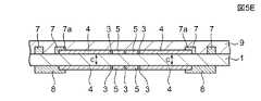
図4は第2の実施の形態としての入力装置(タッチセンサ)の一部を拡大して示す部分断面図、図5Aないし図5Fは、本発明の第2の実施の形態としての第2の製造方法を工程別に示すタッチセンサの部分断面図である。なお、以下においては、第1の実施の形態で示した同一の部材については、同一の符号を付して説明する。 FIG. 4 is an enlarged partial sectional view showing a part of an input device (touch sensor) as a second embodiment, and FIGS. 5A to 5F show a second embodiment as a second embodiment of the present invention. It is a fragmentary sectional view of the touch sensor which shows a manufacturing method according to a process. In the following, the same members shown in the first embodiment will be described with the same reference numerals.
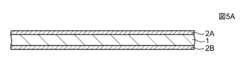
第2の実施の形態に示すタッチセンサTS2(図4参照)が、上記第1の実施の形態に示すタッチセンサTS(図2参照)と異なる点は、前記タッチセンサTS2では主に前記タッチセンサTSが有していた絶縁層6を有さない構成とした点にある。なお、第2の実施の形態に示すタッチセンサTS2のその他の構成は、上記第1の実施の形態に示すタッチセンサTS同様である。 The touch sensor TS2 shown in the second embodiment (see FIG. 4) is different from the touch sensor TS shown in the first embodiment (see FIG. 2) in that the touch sensor TS2 mainly uses the touch sensor TS2. The structure is that the TS does not have the insulating
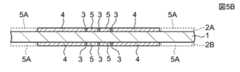
次に、図5Aないし図5Fを用いて、第2の実施の形態に示すタッチセンサTS2の製造方法(第2の製造方法)について説明する。 Next, a manufacturing method (second manufacturing method) of the touch sensor TS2 shown in the second embodiment will be described with reference to FIGS. 5A to 5F.
図5Aに示すように、第1の工程では、上記第1の実施の形態同様に例えばPET(ポリエチレンテレフタレート)などからなる基材1が用意され、前記基材1の表裏両面にITOからなる導電膜2A,2Bを形成する。 As shown in FIG. 5A, in the first step, a
図5Bに示すように、第2の工程では上記第1の実施の形態同様に図示しないレーザ装置を用いて前記導電膜2A,2Bに複数の区画溝3を形成する。これにより、基材1の表裏両面に複数の電極部4(4a〜4o)および配線導電膜5が同一形状および同一配列で形成される。ただし、第2の実施の形態では、前記配線導電膜5のうち、図5Bに破線で示す複数の電極部4(4a〜4o)の両端に位置する配線導電膜5A,5Aは除去されて基板1が露出される点が上記第1に実施の形態と相違している。 As shown in FIG. 5B, in the second step, a plurality of
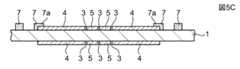
第3の工程では、図5Cに示すように基材1の表面に配線パターン7がAgインクなどを用いて印刷形成される。このとき、配線パターン7の一端7aは電極部4a〜4oのいずれかに接続される。また配線パターン7の他端は前記基材1の表面上を引き回され、上記第1の実施の形態同様に基材1に設けられるフレキシブルケーブル12とのコネクタ13に接続される(図示せず)。 In the third step, as shown in FIG. 5C, the
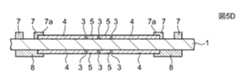
第4の工程では、図5Dに示すように基材1の裏面上にAgインクなどが印刷されて、グランドGND用の導通パターン8が形成される。これにより、基材1の裏面側において前記区画溝3によって分離された複数の電極部4a〜4oおよび配線導電膜5が導通接続される。すなわち、前記導電膜2B全体が電気的に接続され、グランドGNDに設定される。 In the fourth step, as shown in FIG. 5D, Ag ink or the like is printed on the back surface of the
そして、第1の実施の形態同様に、第5の工程では図5Eに示すように最上層に絶縁性を有する透明レジスト材が印刷されて保護層9が形成され、続く第6の工程では図5Fに示すように最下層に絶縁性を有する透明レジスト材が所定の膜厚寸法で印刷されて感度調整層10が形成され、タッチセンサTSが完成する。 As in the first embodiment, in the fifth step, as shown in FIG. 5E, an insulating transparent resist material is printed on the uppermost layer to form the
前記感度調整層10を所定の膜厚で形成することにより、タッチセンサTSを有する電子機器の背面に位置する操作体とグランドGND用の導通パターン8との間の距離を、導通パターン8の電位がふら付かない程度に設定することができる。これにより、タッチセンサTSの誤動作が少なく検出精度を高めることが可能となる。 By forming the
第2の実施の形態に示すタッチセンサTS2では、上記第1の実施の形態に示すタッチセンサTSに比較して、前記絶縁層6を有しない分だけ厚さ寸法を薄くすることが可能である。さらには、第2の実施の形態に示す製造方法では、上記第1の実施の形態に比較して絶縁層6を形成する工程を不要とすることが可能であり、この点で製造コストを安価とすることができる。 In the touch sensor TS2 shown in the second embodiment, the thickness dimension can be reduced by the amount not having the insulating
1 基材
2A,2B 導電膜
3 区画溝3
4,4a〜4o 電極部
5 配線導電膜
6 絶縁層
7 配線パターン
8 導通パターン
9 保護層
10 感度調整層
12 フレキシブルケーブル
20 液晶表示装置
TS タッチセンサ(入力装置)1
4, 4a to 4o
Claims (7)
Translated fromJapanese透明な基材の表裏両面に導電膜が夫々設けられ、
前記基材の表面には、前記導電膜が区画溝によって所定形状に分離されることにより前記センサ部を構成する複数の電極部及び配線導電膜が形成されており、
前記基材の裏面には、前記表面に形成された前記複数の電極部を重ねたときに、同一の形状及び配列で重なり合う複数の電極部及び前記基材の周辺部以外の位置に配置された前記電極部から前記周辺部へ延びる複数の配線導電膜と、前記周辺部に枠状に形成された導通パターンとが設けられ、
前記基材の両面に形成された複数の電極部及び複数の配線導電膜は、前記基材の一方の面から照射されて他方の面に抜けるレーザ光によって前記基材の表裏両面に設けられた導電膜に同時に形成される前記区画溝により分離されたものであり、
前記周辺部に設けられた前記複数の電極部と前記複数の配線導電膜とが前記導通パターンを介して導通接続されて、前記基材の裏面に形成されている全ての前記電極部が同電位に設定されていることを特徴とする入力装置。In an input device having a sensor unit for detecting a capacitance change with an operating body,
Conductive films are provided on both sides of thetransparent base material,
On the surface of the base material, the conductive film is separated into a predetermined shape by a partition groove,and a plurality of electrode partsand a wiring conductive film that form the sensor partare formed ,
On the back surface of thebase material , when the plurality of electrode portions formed on the front surface are overlapped, theyare arranged at positions other than the plurality of electrode portions overlapping in the same shape and arrangement andthe peripheral portion of the base material. A plurality of wiring conductive films extending from the electrode part to the peripheral part, and a conductive pattern formed in a frame shape on the peripheral part are provided,
The plurality of electrode portions and the plurality of wiring conductive films formed on both surfaces of the base material are provided on both front and back surfaces of the base material by laser light that is irradiated from one surface of the base material and exits to the other surface. Separated by the partition grooves formed simultaneously in the conductive film,
The plurality of electrode portions provided in the peripheral portion and the plurality of wiring conductive films are conductively connected through the conductive pattern, and all the electrode portions formed on the back surface of the base material have the same potential. An input device characterizedby being set to .
(a)透明な基材の両面に導電膜を形成する工程、
(b) レーザ光を一方の導電膜に向けて照射して前記両面の導電膜に対して同時に区画溝を形成し、複数の所定形状の区画からなる前記センサ部を構成する電極部と配線導電膜を形成する工程、
(c) 前記一方の導電膜に形成された一部の前記配線導電膜上に絶縁層を形成する工程、
(d) 絶縁層上に、前記個々の電極部の夫々に対して電気的に接続される配線パターンを形成する工程、
(e) 他方の導電膜に、前記区画溝により分離された個々の電極部間を導通接続する導通パターンを形成する工程、
の順で行われることを特徴とする入力装置の製造方法。In the manufacturing method of the input device having the sensor unit for detecting the capacitance change with the operating body,
(A) forming a conductive film on both surfaces of atransparent substrate;
(B) A laser beam is irradiated towardone of the conductive films to form partition groovessimultaneously on the conductive films on both sides, and the electrode section and the wiring conductor constituting the sensor section composed of a plurality of sections having a predetermined shape a process thatform the membrane,
(C) forming an insulating layer on a part of the wiring conductive film formed on the one conductive film;
(D) forming a wiring pattern electrically connected to each of the individual electrode portions on the insulating layer;
(E) forming a conductive pattern for conductively connecting the individual electrode parts separated by the partitioning groove on the other conductive film;
The manufacturing method of the input device characterizedby thesebeing performed in order .
(f) 前記一方の導電膜を透明な絶縁層で覆う工程、
(g) 前記他方の導電膜を透明な絶縁層で覆う工程、
を有する請求項4記載の入力装置の製造方法。After the step (e),
(F) step of covering with a transparent insulating layerprior SL one conductive film,
(G) covering the other conductive film with a transparent insulating layer;
The manufacturing method of the input device of Claim4 which has these.
Priority Applications (2)
| Application Number | Priority Date | Filing Date | Title |
|---|---|---|---|
| JP2006325611AJP4332174B2 (en) | 2006-12-01 | 2006-12-01 | Input device and manufacturing method thereof |
| US11/945,836US20080129317A1 (en) | 2006-12-01 | 2007-11-27 | Input device and method of manufacturing the same |
Applications Claiming Priority (1)
| Application Number | Priority Date | Filing Date | Title |
|---|---|---|---|
| JP2006325611AJP4332174B2 (en) | 2006-12-01 | 2006-12-01 | Input device and manufacturing method thereof |
Publications (2)
| Publication Number | Publication Date |
|---|---|
| JP2008140130A JP2008140130A (en) | 2008-06-19 |
| JP4332174B2true JP4332174B2 (en) | 2009-09-16 |
Family
ID=39474973
Family Applications (1)
| Application Number | Title | Priority Date | Filing Date |
|---|---|---|---|
| JP2006325611AExpired - Fee RelatedJP4332174B2 (en) | 2006-12-01 | 2006-12-01 | Input device and manufacturing method thereof |
Country Status (2)
| Country | Link |
|---|---|
| US (1) | US20080129317A1 (en) |
| JP (1) | JP4332174B2 (en) |
Families Citing this family (63)
| Publication number | Priority date | Publication date | Assignee | Title |
|---|---|---|---|---|
| US7663607B2 (en) | 2004-05-06 | 2010-02-16 | Apple Inc. | Multipoint touchscreen |
| CN104965621B (en) | 2006-06-09 | 2018-06-12 | 苹果公司 | Touch screen LCD and its operating method |
| US8259078B2 (en) | 2006-06-09 | 2012-09-04 | Apple Inc. | Touch screen liquid crystal display |
| CN102981678B (en) | 2006-06-09 | 2015-07-22 | 苹果公司 | Touch screen liquid crystal display |
| US9710095B2 (en) | 2007-01-05 | 2017-07-18 | Apple Inc. | Touch screen stack-ups |
| WO2009154794A1 (en)* | 2008-06-20 | 2009-12-23 | University Of Central Florida Research Foundation, Inc. | Solar energy converter with improved photovoltaic efficiency, frequency conversion and thermal management permiting super highly concentrated cellection |
| US20100066683A1 (en)* | 2008-09-17 | 2010-03-18 | Shih-Chang Chang | Method for Transferring Thin Film to Substrate |
| JP5263766B2 (en)* | 2008-09-17 | 2013-08-14 | 株式会社ザクティ | Capacitive touchpad device |
| JP2010198615A (en)* | 2009-02-20 | 2010-09-09 | Acrosense Technology Co Ltd | Capacitive touch panel |
| JP4775722B2 (en)* | 2009-02-23 | 2011-09-21 | 大日本印刷株式会社 | Touch panel sensor, laminate for manufacturing touch panel sensor, and method for manufacturing touch panel sensor |
| US9317140B2 (en) | 2009-03-30 | 2016-04-19 | Microsoft Technology Licensing, Llc | Method of making a multi-touch input device for detecting touch on a curved surface |
| US8982051B2 (en) | 2009-03-30 | 2015-03-17 | Microsoft Technology Licensing, Llc | Detecting touch on a surface |
| JP5366051B2 (en) | 2009-04-20 | 2013-12-11 | 株式会社ジャパンディスプレイ | Information input device, display device |
| US8956718B2 (en) | 2009-06-19 | 2015-02-17 | Apple Inc. | Transparent conductor thin film formation |
| JP5486854B2 (en)* | 2009-06-29 | 2014-05-07 | 株式会社ジャパンディスプレイ | Information input device, display device |
| JP5473456B2 (en)* | 2009-07-29 | 2014-04-16 | 京セラ株式会社 | Capacitive touch panel and display device including the same |
| GB2472613B (en)* | 2009-08-11 | 2015-06-03 | M Solv Ltd | Capacitive touch panels |
| CN102648446B (en) | 2009-10-23 | 2016-01-20 | 万佳雷射有限公司 | Capacitive touch screen |
| JP5300684B2 (en)* | 2009-10-27 | 2013-09-25 | 株式会社ジャパンディスプレイウェスト | Capacitance input device, method of manufacturing capacitance input device, and electro-optical device with input function |
| KR20120117762A (en)* | 2009-11-27 | 2012-10-24 | 도판 인사츠 가부시키가이샤 | Transparent conductive laminate, method for producing same, and electrostatic capacitance type touch panel |
| WO2011070801A1 (en) | 2009-12-10 | 2011-06-16 | 凸版印刷株式会社 | Conductive substrate, method for producing same, and touch panel |
| JP5606093B2 (en)* | 2010-02-17 | 2014-10-15 | アルプス電気株式会社 | Input device |
| TW201145132A (en)* | 2010-03-11 | 2011-12-16 | Alps Electric Co Ltd | Translucent inputting device |
| CN101807133A (en)* | 2010-03-22 | 2010-08-18 | 牧东光电(苏州)有限公司 | Method for processing induction layer of touch panel |
| TWI474377B (en)* | 2010-03-25 | 2015-02-21 | Winsky Technology Ltd | A method of patterning a substrate and a method of manufacturing a capacitive touch panel |
| CN102236484B (en)* | 2010-04-30 | 2015-03-11 | 永恒科技有限公司 | Method for patterning substrate and method for manufacturing capacitive touch panel |
| US8723046B2 (en) | 2010-06-22 | 2014-05-13 | Nissha Printing Co., Ltd. | Narrow frame touch input sheet with good anticorrosion property and manufacturing method thereof |
| KR101525953B1 (en) | 2010-11-30 | 2015-06-09 | 닛토덴코 가부시키가이샤 | Display panel device having touch input function |
| JP5715393B2 (en)* | 2010-12-06 | 2015-05-07 | クラリオン株式会社 | Touch panel device and in-vehicle device |
| US8804056B2 (en) | 2010-12-22 | 2014-08-12 | Apple Inc. | Integrated touch screens |
| JP5490034B2 (en)* | 2011-02-08 | 2014-05-14 | 信越ポリマー株式会社 | Method for manufacturing conductive pattern forming substrate and conductive pattern forming substrate |
| GB2487962B (en)* | 2011-02-11 | 2016-10-12 | M-Solv Ltd | Method for making a two-layer capacitive touch sensor panel |
| TWI428667B (en) | 2011-06-09 | 2014-03-01 | Shih Hua Technology Ltd | Method for making touch panel |
| TWI447978B (en) | 2011-06-09 | 2014-08-01 | Shih Hua Technology Ltd | Method for making touch panel |
| TWI457808B (en) | 2011-06-09 | 2014-10-21 | Shih Hua Technology Ltd | Touch screen |
| TWI425562B (en) | 2011-06-09 | 2014-02-01 | Shih Hua Technology Ltd | Method for making touch panel |
| TWI512555B (en)* | 2011-06-09 | 2015-12-11 | Shih Hua Technology Ltd | Touch panel and method for making the same |
| TWI528388B (en) | 2011-06-09 | 2016-04-01 | 識驊科技股份有限公司 | Pattern conductive element |
| KR101373088B1 (en)* | 2011-09-08 | 2014-03-11 | 히타치 어플라이언스 가부시키가이샤 | Refrigerator |
| CN103959216A (en) | 2011-10-25 | 2014-07-30 | 尤尼皮克塞尔显示器有限公司 | Polarizer capacitive touch screen |
| US9256311B2 (en)* | 2011-10-28 | 2016-02-09 | Atmel Corporation | Flexible touch sensor |
| CN103105962B (en)* | 2011-11-09 | 2016-04-06 | 宸鸿科技(厦门)有限公司 | Contact panel, touch electrode structure and preparation method thereof |
| JP2013109460A (en)* | 2011-11-18 | 2013-06-06 | Shin Etsu Polymer Co Ltd | Transparent wiring sheet |
| CN102981060B (en)* | 2012-09-07 | 2014-12-03 | 清华大学 | Graphene quantum capacity measurement device and preparing method thereof |
| CN102929470A (en)* | 2012-11-21 | 2013-02-13 | 南京华显高科有限公司 | Method and structure for improving anti-interference of capacitive touch screen |
| JP2014109991A (en)* | 2012-12-04 | 2014-06-12 | Panasonic Corp | Touch panel, touch panel unit and electronic apparatus |
| GB2509985A (en)* | 2013-01-22 | 2014-07-23 | M Solv Ltd | Method of forming patterns on coatings on opposite sides of a transparent substrate |
| JPWO2014132623A1 (en)* | 2013-02-27 | 2017-02-02 | 凸版印刷株式会社 | Touch panel and touch panel manufacturing method |
| JP2014170334A (en)* | 2013-03-04 | 2014-09-18 | Alps Electric Co Ltd | Capacitance touch panel, and handheld electronic apparatus using the same |
| DE102013104644B4 (en)* | 2013-05-06 | 2020-06-04 | Polylc Gmbh & Co. Kg | Layer electrode for touch screens |
| US9140737B2 (en)* | 2013-05-21 | 2015-09-22 | Nokia Technologies Oy | Capacitive touch sensor |
| TWI502429B (en)* | 2013-06-13 | 2015-10-01 | Sipix Technology Inc | Touch-control display and fabrication method thereof |
| JP6307766B2 (en)* | 2014-02-21 | 2018-04-11 | 積水ポリマテック株式会社 | Touch sensor manufacturing method and touch sensor |
| GB2529156B (en) | 2014-08-08 | 2018-02-07 | M-Solv Ltd | Double far-side laser ablation |
| JP6563254B2 (en)* | 2015-06-03 | 2019-08-21 | 日東電工株式会社 | Laminated body, method for manufacturing touch panel sensor, and touch panel sensor |
| JP6431610B2 (en) | 2015-08-18 | 2018-11-28 | アルプス電気株式会社 | Capacitive input device |
| JP6610159B2 (en)* | 2015-10-20 | 2019-11-27 | Tdk株式会社 | Thin film capacitor |
| JP6986393B2 (en)* | 2016-11-15 | 2021-12-22 | ビアメカニクス株式会社 | Substrate processing method |
| CN109144333A (en)* | 2017-06-15 | 2019-01-04 | 上海峰宁信息科技股份有限公司 | A kind of method that the realization of metal mesh opening touch control film electronic blackboard is bonded entirely |
| CN116540891A (en) | 2017-08-01 | 2023-08-04 | 株式会社和冠 | Sensor for detecting pen signal sent by pen |
| JP7059042B2 (en)* | 2018-01-10 | 2022-04-25 | 株式会社ワコム | Sensor panel |
| JP6733693B2 (en)* | 2018-03-19 | 2020-08-05 | Smk株式会社 | Touch panel manufacturing method |
| CN109633278B (en)* | 2018-12-25 | 2021-05-14 | 伟宸科技(武汉)有限公司 | Capacitor device |
Family Cites Families (10)
| Publication number | Priority date | Publication date | Assignee | Title |
|---|---|---|---|---|
| US4090092A (en)* | 1976-07-16 | 1978-05-16 | General Electric Company | Shielding arrangement for a capacitive touch switch device |
| GB2244164A (en)* | 1990-05-18 | 1991-11-20 | Philips Electronic Associated | Fingerprint sensing |
| US5420428A (en)* | 1993-05-05 | 1995-05-30 | Radiant Technologies, Inc. | Infra-red sensing array |
| GB9725571D0 (en)* | 1997-12-04 | 1998-02-04 | Philips Electronics Nv | Electronic apparatus comprising fingerprint sensing devices |
| US6222376B1 (en)* | 1999-01-16 | 2001-04-24 | Honeywell International Inc. | Capacitive moisture detector and method of making the same |
| US7256589B2 (en)* | 2001-04-27 | 2007-08-14 | Atrua Technologies, Inc. | Capacitive sensor system with improved capacitance measuring sensitivity |
| TW583592B (en)* | 2002-04-03 | 2004-04-11 | Lightuning Tech Inc | Capacitive fingerprint sensor |
| US7609178B2 (en)* | 2006-04-20 | 2009-10-27 | Pressure Profile Systems, Inc. | Reconfigurable tactile sensor input device |
| US8354143B2 (en)* | 2005-05-26 | 2013-01-15 | Tpk Touch Solutions Inc. | Capacitive touch screen and method of making same |
| US20080047764A1 (en)* | 2006-08-28 | 2008-02-28 | Cypress Semiconductor Corporation | Temperature compensation method for capacitive sensors |
- 2006
- 2006-12-01JPJP2006325611Apatent/JP4332174B2/ennot_activeExpired - Fee Related
- 2007
- 2007-11-27USUS11/945,836patent/US20080129317A1/ennot_activeAbandoned
Also Published As
| Publication number | Publication date |
|---|---|
| JP2008140130A (en) | 2008-06-19 |
| US20080129317A1 (en) | 2008-06-05 |
Similar Documents
| Publication | Publication Date | Title |
|---|---|---|
| JP4332174B2 (en) | Input device and manufacturing method thereof | |
| EP3089008B1 (en) | Touch input device | |
| CN105260058B (en) | Electrode slice for detecting pressure and the touch input device including the electrode slice | |
| EP3048514B1 (en) | Touch input device | |
| EP2980685B1 (en) | Touch input device | |
| US9006598B2 (en) | Conductive structure and method of manufacturing the same | |
| US8717332B2 (en) | Planar element, and touch switch | |
| US9411473B2 (en) | Touch device and manufacturing method thereof | |
| US20170102823A1 (en) | Electrode sheet and touch input device | |
| US8643607B2 (en) | Touch panel and manufacturing method of the same | |
| CN106802746B (en) | Touch panel and image display device including the same | |
| US20100053114A1 (en) | Touch panel apparatus and method for manufacturing the same | |
| JP2008225821A (en) | Input device | |
| JP2009169720A (en) | Touch sensor | |
| KR20160048424A (en) | Touch input device | |
| CN108664158B (en) | touch display | |
| CN206209685U (en) | A kind of touch display screen and display device | |
| TW201837678A (en) | Wiring body, wiring board and touch sensor | |
| CN110275650B (en) | Touch sensing device, touch display panel and touch display panel mother board | |
| KR102082485B1 (en) | Transparent electrode and electronic device including the same | |
| KR20160034240A (en) | Smartphone | |
| KR101077675B1 (en) | Manufacturing apparatus of coordinate detecting device | |
| CN111045553A (en) | Touch display panel and touch display device | |
| US20090283339A1 (en) | Coordinate detecting device | |
| KR101734989B1 (en) | Touch input device |
Legal Events
| Date | Code | Title | Description |
|---|---|---|---|
| A621 | Written request for application examination | Free format text:JAPANESE INTERMEDIATE CODE: A621 Effective date:20080828 | |
| A977 | Report on retrieval | Free format text:JAPANESE INTERMEDIATE CODE: A971007 Effective date:20090105 | |
| A131 | Notification of reasons for refusal | Free format text:JAPANESE INTERMEDIATE CODE: A131 Effective date:20090120 | |
| A521 | Written amendment | Free format text:JAPANESE INTERMEDIATE CODE: A523 Effective date:20090313 | |
| TRDD | Decision of grant or rejection written | ||
| A01 | Written decision to grant a patent or to grant a registration (utility model) | Free format text:JAPANESE INTERMEDIATE CODE: A01 Effective date:20090616 | |
| A01 | Written decision to grant a patent or to grant a registration (utility model) | Free format text:JAPANESE INTERMEDIATE CODE: A01 | |
| A61 | First payment of annual fees (during grant procedure) | Free format text:JAPANESE INTERMEDIATE CODE: A61 Effective date:20090619 | |
| R150 | Certificate of patent or registration of utility model | Free format text:JAPANESE INTERMEDIATE CODE: R150 | |
| FPAY | Renewal fee payment (event date is renewal date of database) | Free format text:PAYMENT UNTIL: 20120626 Year of fee payment:3 | |
| LAPS | Cancellation because of no payment of annual fees |