JP4332113B2 - Direct conversion receiver - Google Patents
Direct conversion receiverDownload PDFInfo
- Publication number
- JP4332113B2 JP4332113B2JP2004531927AJP2004531927AJP4332113B2JP 4332113 B2JP4332113 B2JP 4332113B2JP 2004531927 AJP2004531927 AJP 2004531927AJP 2004531927 AJP2004531927 AJP 2004531927AJP 4332113 B2JP4332113 B2JP 4332113B2
- Authority
- JP
- Japan
- Prior art keywords
- signal
- direct conversion
- conversion receiver
- phase
- baseband
- Prior art date
- Legal status (The legal status is an assumption and is not a legal conclusion. Google has not performed a legal analysis and makes no representation as to the accuracy of the status listed.)
- Expired - Fee Related
Links
- 238000006243chemical reactionMethods0.000titleclaimsdescription40
- 230000010363phase shiftEffects0.000claimsdescription19
- 230000010355oscillationEffects0.000claimsdescription16
- 238000000034methodMethods0.000claimsdescription14
- 230000003044adaptive effectEffects0.000claimsdescription2
- 238000010586diagramMethods0.000description7
- 238000004891communicationMethods0.000description4
- 238000005070samplingMethods0.000description2
- 230000005540biological transmissionEffects0.000description1
- 239000006227byproductSubstances0.000description1
- 230000001934delayEffects0.000description1
- 238000001514detection methodMethods0.000description1
- 238000004519manufacturing processMethods0.000description1
- 239000000047productSubstances0.000description1
Images


Classifications
- H—ELECTRICITY
- H04—ELECTRIC COMMUNICATION TECHNIQUE
- H04B—TRANSMISSION
- H04B1/00—Details of transmission systems, not covered by a single one of groups H04B3/00 - H04B13/00; Details of transmission systems not characterised by the medium used for transmission
- H04B1/06—Receivers
- H04B1/16—Circuits
- H04B1/26—Circuits for superheterodyne receivers
- H—ELECTRICITY
- H04—ELECTRIC COMMUNICATION TECHNIQUE
- H04B—TRANSMISSION
- H04B1/00—Details of transmission systems, not covered by a single one of groups H04B3/00 - H04B13/00; Details of transmission systems not characterised by the medium used for transmission
- H04B1/06—Receivers
- H04B1/16—Circuits
- H04B1/30—Circuits for homodyne or synchrodyne receivers
Landscapes
- Engineering & Computer Science (AREA)
- Computer Networks & Wireless Communication (AREA)
- Signal Processing (AREA)
- Superheterodyne Receivers (AREA)
Description
Translated fromJapanese本発明はダイレクトコンバージョン受信機に関し、より詳しくはDCオフセット成分を軽減するダイレクトコンバージョン受信機アーキテクチャに関する。 The present invention relates to a direct conversion receiver, and more particularly to a direct conversion receiver architecture that reduces DC offset components.
従来のラジオ受信機は一般的にスーパーヘテロダイン・アーキテクチャを採用している。そのようなアーキテクチャでは、受信機は受信したRF信号を中間周波数(IF)にダウンコンバートする。更なる処理を経て、IF信号はベースバンド信号へ変換される。一方、ダイレクトコンバージョン受信機は受信したRF信号をたった1回の処理でベースバンドに変換する。なぜならダイレクトコンバージョン受信機はRF信号を中間周波数に変換しないからであり、それらは”ゼロIF”受信機としても知られる。受信機の各処理段階は必然的に雑音を生成し多くのコンポーネントを必要とするとすれば、相当の努力がダイレクトコンバージョン受信機の設計に注がれている。 Conventional radio receivers generally employ a superheterodyne architecture. In such an architecture, the receiver downconverts the received RF signal to an intermediate frequency (IF). Through further processing, the IF signal is converted into a baseband signal. On the other hand, the direct conversion receiver converts the received RF signal into baseband by a single process. Because direct conversion receivers do not convert RF signals to intermediate frequencies, they are also known as "zero IF" receivers. Given that each processing stage of the receiver inevitably generates noise and requires many components, considerable effort is devoted to the design of direct conversion receivers.
ダイレクトコンバージョン受信機の魅力に富むS/N、及び生産上の利点にも関わらず、局部発振(LO)の自己混合(self-mixing)から発生するDCオフセットの問題、LOの低雑音増幅器(LNA)への漏れ、偶数次の歪み、及びAM信号を妨害する包路線検波のために、無線端末のようなほとんどの活用はスーパーヘテロダイン受信方式を使い続けている。また、重要な問題はLOの1/fノイズ、相互混合(reciprocal mixing)、及びLOのスプリアス信号から発生する。 Despite the attractive S / N and production advantages of direct conversion receivers, the problem of DC offsets arising from local oscillation (LO) self-mixing, LO low noise amplifier (LNA) ), Even order distortion, and envelope detection that interferes with AM signals, most applications such as wireless terminals continue to use superheterodyne reception schemes. Important issues also arise from LO 1 / f noise, reciprocal mixing, and LO spurious signals.
LOの自己混合はダイレクトコンバージョン受信機に次のように発生する。ミキサは1つの端子に搬送周波数で受信したRF信号を受信し、他方の端子にも搬送周波数かそれに近い周波数のLO信号を受信する。この局部発振信号は一般的に受信したRF信号よりも非常に大きな電力であり、不可避的反動的にRF端子に伝わる。このようにして自己混合する。この自己混合の過程において、LO信号のような正弦波は調和して、DCオフセット成分を生成する。そのようなベースバンドのDCオフセット成分は、特に現代デジタル通信システムに共通の高速処理においてデジタル信号の復調を妨害する。 LO self-mixing occurs in the direct conversion receiver as follows. The mixer receives the RF signal received at the carrier frequency at one terminal and the LO signal at or near the carrier frequency at the other terminal. This local oscillation signal is generally much larger in power than the received RF signal, and inevitably reacts to the RF terminal. Self-mixing in this way. In this self-mixing process, sine waves such as LO signals harmonize to produce a DC offset component. Such baseband DC offset components interfere with the demodulation of digital signals, especially in the high speed processing common to modern digital communication systems.
従って、DCオフセットの問題を軽減するダイレクトコンバージョン受信機を改良する技術が必要である。 Therefore, there is a need for a technique for improving a direct conversion receiver that reduces the problem of DC offset.
本発明の第1の態様に従って、ダイレクトコンバージョン受信機は局部発振信号を提供する発振器を含む。移相器はLO信号を受信して前記LO信号と実質的に90°の位相差を有する移相信号を提供するために形成される。受信機はLO信号と入力RF信号とを混合し、ミキサの第1入力端子に混合信号を提供する。ミキサは移相信号を受信するための第2の端子を含み、第1の入力端子及び第2の入力端子へ入力される信号の乗算信号(product)であるベースバンド出力信号を提供する。In accordance with a first aspect of the invention, a direct conversion receiver includes an oscillator that provides a local oscillation signal. A phase shifter is configured to receive the LO signal and provide aphase shift signal having a phase difference of substantially 90 ° with the LO signal. The receiver mixes the LO signal and the input RF signal and provides the mixed signal to the first input terminal of the mixer. The mixer includes a second terminal for receiving thephase-shifted signal and provides a baseband output signal that is a product of signals input to the first input terminal and the second input terminal.
本発明の他の態様に従って、RF信号を直接ダウンコンバートする方法を提供する。この方法では、前記RF信号は混合信号を生成するためにLO信号と混合される。前記LO信号はまた、直交信号を提供するために実質的に90°移相される。前記直交信号と前記混合信号はベースバンド出力信号を生成するため互いに掛け合わされる。 In accordance with another aspect of the present invention, a method for directly downconverting an RF signal is provided. In this method, the RF signal is mixed with the LO signal to produce a mixed signal. The LO signal is also phase shifted substantially 90 ° to provide a quadrature signal. The quadrature signal and the mixed signal are multiplied together to produce a baseband output signal.
本発明は添付した図面と一体である以下の詳細な説明を考慮したときに、より完全に理解されるであろう。 The present invention will be more fully understood when the following detailed description is considered in conjunction with the accompanying drawings.
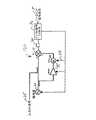
図1はミキサ20からのベースバンド信号出力15のDCオフセット成分を軽減するダイレクトコンバージョン受信機10のブロック図である。ミキサ20は両側波帯及び側波帯のいずれかでよく、そのベースバンド信号出力は、そのRF入力端子21及び局部発振(LO)入力端子22の入力との乗算信号を表す。ダイレクトコンバージョン受信機10は、ミキサ20のRF入力端子21へ接続される搬送周波数の入力RF信号25を受信する。入力RF信号25はアンテナ(図示されていない)で受信され、ミキサ20に接続される前に、ダイレクトコンバージョン受信機先行技術において慣習的に行われるようにフィルタ及び低雑音増幅器による処理を経てもよい。ダイレクトコンバージョン受信機10は信号源30を含み、これは電圧制御発振器(VCO)又は適切なLO出力の似たような発振器であってよい。例えば、これは正弦波出力35であってよい。LO出力のタイプは入力RF信号25に含まれる特殊な変調に依存するであろうことは当業者に認識されるであろう。正弦波出力35及び入力RF信号25は、ミキサ20のRF入力端子に接続する前にRF結合器40を通して混合される。RF結合器40の設計は、入力RF信号25及び正弦波出力35を伝搬するために選定された導波管のタイプ(ストリップ線路、同軸ケーブル、又はマイクロストリップのような)に依存し、当業者に良く知られている。言い換えると、用いられる導波管のタイプは搬送周波数、信号電力値、空間関係、及び他の良く知られた設計上の選択に依存する。FIG. 1 is a block diagram of a
RF入力端子21への接続に加えて、正弦波出力35はRF結合器55へも接続される。RF結合器55の代わりに信号分配器を使用してもよいことは認識されるであろう。正弦波出力35はこのRF結合器55を通って移相器45へ接続される。移相器45は、ミキサ20のLO入力端子22へ直交局部発振信号50を提供するために、正弦波出力35を90°移相するよう設定される。移相器45は個別部品として示されているが、ミキサ20と一体であってよい。そのような設計は、直交局部発振信号50がRF入力端子21へ伝わりこれにより自己混合をしてベースバンド信号出力15における不要なDCオフセット成分を生成する機会を最小化する。もう1つの方法として、直交局部発振信号50がRF入力端子21へ放出的に又は反動的に伝達するのを最小化するため、移相器45をミキサ20のLO入力端子22にできるだけ近くに配置すればよい。 In addition to the connection to the
有利なことに、源信号35及び直交局部発振信号50は、以下の数学的算出により表されるベースバンド信号出力15にDCオフセット成分を生成しない。RF端子21への入力をfr(t)と、LO入力端子22への入力をfl(t)と、ベースバンド信号出力15をfx(t)とすると、
fx(t)=(mfr(t))*(nfl(t))となり、
ここで、m,n=...,−2,−1,0,1,2,...であり、
以下の算出においては、簡単にするためにm=n=1だと仮定するが、異なる値をとっても類似する結果となる。搬送周波数をωRFと、キャリア位相をψRFとし、入力RF信号25が、fRF(t)=Acos(ωRFt+ψRF)で表され、正弦波出力35が、Bcos(ωLOt)で表されるなら、
fr(t)=Acos(ωRFt+ψRF)+Bcos(ωLOt)
となる。
正弦波出力35が上記のように与えられるとすれば、直交局部発振信号は、理想的には、Bsin(ωLOt)として表される。しかし、移相誤差及び、振幅損失又は利得を考慮するため、移相器45により提供される移相をψbとすると、直交局部発振信号はCcos(ωLOt−ψb)により表される。直交誤差項をεbとし、ψb=90°−εbとしてこれらの式を考えると、fX(t)は、DCオフセット項、2倍周波数項、DC周波数オフセット項、及び2倍周波数オフセット・プラス・オフセット項の合計として表されることとなる。Advantageously, the source signal 35 and the quadrature local oscillator signal 50 do not generate a DC offset component in the
fx (t) = (mfr (t)) * (nfl (t))
Where m, n = ..., -2, -1, 0, 1, 2, ...,
In the following calculation, it is assumed that m = n = 1 for simplicity, but similar results are obtained even if different values are taken. The carrier frequency is ωRF , the carrier phase is ψRF , the input RF signal 25 is represented by fRF (t) = A cos (ωRF t + ψRF ), and the sine wave output 35 is B cos (ωLO t). If represented
fr (t) = A cos (ωRF t + φRF ) + B cos (ωLO t)
It becomes.
If the sine wave output 35 is given as described above, the orthogonal local oscillation signal is ideally represented as Bsin (ωLO t). However, in order to consider thephase shift error and the amplitude loss or gain, if the phase shift provided by the
DCオフセット項
fX(t)=(AB/2)(cos(εb−90°))
2倍周波数項
+(AB/2)cos(2ωLOt+90°−εb))
周波数オフセット項
+(BC/2)cos((ωRF−ωLO)t+ψRF−90°+εb)
2倍周波数プラス・オフセット項
+(BC/2)cos(2(ωRF+ωLO)t+ψRF+90°+εb)DC offset term fX (t) = (AB / 2) (cos (εb −90 °))
Double frequency term
+ (AB / 2) cos (2ωLO t + 90 ° −εb ))
Frequency offset term
+ (BC / 2) cos ((ωRF −ωLO ) t + ψRF −90 ° + εb )
Double frequency plus offset term
+ (BC / 2) cos (2 (ωRF + ωLO ) t + ψRF + 90 ° + εb )
2倍周波数(高周波数)項は容易にフィルタされ、又は他の方法で除去される。仮に移相器45が直交誤差項をゼロ若しくは非常に小さく保つように形成されているならば、DCオフセット項はゼロ若しくは非常に小さなものである。これは周波数オフセット項だけを残し、この項はωRFとωLO間の差だけDCから周波数オフセットしたダウンコンバートされた入力RF信号を表す。そして受信機10からのベースバンド信号出力は、(BC/2)cos((ωRF−ωLO)t+ψRF−90°+εb)として表されうる。Double frequency (high frequency) terms are easily filtered or otherwise removed. If the
前記DCオフセット項は、直交誤差項がゼロ若しくは非常に小さいものであるときにだけ軽減される。仮にεb−90°<−90°である場合、前記DCオフセット項はマイナスになることに注意されたい。逆にεb−90°>−90°である場合、前記DCオフセット項はプラスになる。図2において、この特性は移相フィードバックループ60が移相器45を制御する指令を送り、直交誤差項εbを十分に小さく保ち、ベースバンド信号出力15におけるDCオフセット成分を軽減する。例えば、移相フィードバックループ60はオンオフ制御ループを形成してよく、仮にDCオフセット成分がプラスであれば移相器45が追加の所定の遅延量、例えば1°位相を遅らせて直交局部発振信号を調整する。逆に、仮にDCオフセット成分がマイナスであれば移相器45は所定の量、例えば1°位相を進めて直交局部発振信号を調整する。所定の移相量を使用する方法よりも、移相量が予定されないような適応性のある制御方法又はファジー制御方法を使用してもよい。図2に示したダイレクトコンバージョン受信機100には、信号源30は電圧制御発振器(VCO)65によって表されている。The DC offset term is reduced only when the orthogonal error term is zero or very small. Note that if εb −90 ° <−90 °, the DC offset term is negative. Conversely, if εb −90 °> −90 °, the DC offset term is positive. In FIG. 2, this characteristic sends a command for the phase
ベースバンド信号出力15はアナログ信号なので,移相制御ループ60をアナログドメインで実行してよい。もう1つの方法として、ベースバンド信号出力15をデジタル化して、移相制御ループ60をデジタルドメインで実行してもよい。図3において、ダイレクトコンバージョン受信機110は、ベースバンド信号出力15をデジタル化するアナログ−デジタル・コンバーター70を含む。デジタル信号プロセッサ80は、デジタル化されたベースバンド信号出力15を受信し(低域通過フィルタ又は2倍周波数成分を除去する帯域通過フィルタは図示されていないことに注意されたい)、DC周波数オフセット項及びDCオフセット項を検波するために離散フーリエ変換(DFT)を行う。DFTのサンプリング周波数は、エイリアシングを生じずにDC周波数オフセット項を検波するのに適した大きさのDFTウィンドウをかけるために選択されればよい。適切なサンプリング周波数は、搬送周波数ωRFと正弦波出力/局部発振周波数ωLOの間の差に依存する。例えば、PCS(Personal Communication Services)のアプリケーションではωRFは1.8GHzでありえ、この場合ωLOはωRFマイナス・オフセット(20MHzのような)にセットされうる。そしてDFTウィンドウをおよそ25MHzに設定することができる。DC周波数オフセット成分の検波に加えて、前記DFTをDCオフセット項の大きさ及び相(プラス又はマイナス)を検波するために用いることもできる。そして、検波したDCオフセット項を前述したように移相器45を調整する移相制御ループ60に用いてよい。Since the
ここに開示したダイレクトコンバージョン受信機は、I/Q変調通信システムの同相(I)アーム(arm)および直交(Q)アーム双方に実施されてもよいことに注意されたい。通信システムのIアームとQアーム間の利得及び不整合が復調信号にイメージ及び他の不要な副産物を生成することは良く知られている。従って、ダイレクトコンバージョン受信機120はデジタル制御された減衰器72を含み、直交局部発振信号50の振幅を調整してこれらイメージを最小化する。図4において、減衰器72の代わりにデジタル制御された増幅器75を用いてダイレクトコンバージョン受信機120を形成してもよい。増幅器75はプラス又はマイナス利得の一方を有すればよく、必要に応じて直交局部発振信号50の振幅に作用すればよい。代わりに、図5のダイレクトコンバージョン受信機140に示すようにデジタル制御された増幅器75を配置してRF出力35を調整してもよい。更に代わりとして、図6のダイレクトコンバージョン受信機150に示すようにデジタル制御された増幅器75により両信号を調整してもよい。Note that the direct conversion receiver disclosed herein may be implemented in both in-phase (I) and quadrature (Q) arms of an I / Q modulation communication system. It is well known that gains and mismatches between the I and Q arms of a communication system produce images and other unwanted by-products in the demodulated signal. Accordingly, the
従って、本発明は特定の実施態様について説明されたが、この説明は本発明の適用の一例であるだけであってこれに限定されるものではない。その結果、本発明の範囲は特許請求の範囲に記載される。 Thus, although the invention has been described with reference to specific embodiments, this description is only an example of the invention's application and should not be taken as a limitation. As a result, the scope of the invention is set forth in the appended claims.
Claims (14)
Translated fromJapanese局部発振(LO)信号を提供する発振器と、
前記LO信号を受信して前記LO信号と実質的に90°の位相差を有する移相信号を提供する移相器と、
前記LO信号及びRF信号の双方を受信する第1の入力端子、及び前記移相信号を受信する第2の端子を有し、前記第1の入力端子へ入力される信号と前記第2の入力端子へ入力される信号の乗算信号(product)であるベースバンド出力信号を提供するミキサとを有することを特徴とするダイレクトコンバージョン受信機。A direct conversion receiver,
An oscillator that provides a local oscillation (LO) signal;
Aphase shifter that receives the LO signal and provides aphase shift signal having a phase difference of substantially 90 ° with the LO signal;
A first input terminal that receives both the LO signal and the RF signal, and a second terminal that receives thephase-shifted signal, anda signal input to the firstinput terminal and the second input direct conversion receiver; and a mixer to provide a baseband output signal is asignal of the multiplication signal (product) to be inputted to the terminal.
ダウンコンバートによりRF信号から生成された信号を、前記RF信号の周波数とLO信号の周波数の間の差によって測定される離散周波数で検波することができ、且つデジタル化された前記ベースバンド出力信号を処理するデジタル信号プロセッサとを更に有することを特徴とする請求項1に記載のダイレクトコンバージョン受信機。An analog-to-digital converter for digitizing the baseband output signal;
The signal generated from the RF signal by down-conversion can be detected at a discrete frequency measured bythe difference between the frequency of the RF signal andthe frequency of the LO signal , and the digitized baseband output signal is The direct conversion receiver according to claim 1, further comprising a digital signal processor for processing.
(a)移相信号を生成するために局部発振(LO)信号を実質的に90°移相する過程と、
加算信号を生成するために前記RF信号を前記LO信号に混合する過程と、
ベースバンド信号出力を生成するために前記加算信号と前記移相信号の乗算信号を形成する過程とを有することを特徴とする方法。A method for directly down-converting an RF signal,
(A) a process of substantially shifting the local oscillation(LO) signal by 90 ° to generate aphase shift signal;
Comprising the steps of mixingthe RF signaltothe LOsignal to produce asum signal,
Method characterized by having a process of forming a product signalof theaddition signaland thephasesignal to generate a baseband signal output.
検波した前記DCオフセットを最小化するために、過程(a)によって生成された前記移相信号の移相量を調整する過程とを更に有することを特徴とする請求項11に記載の方法。Detecting a DC offset of the baseband signal output;
The method of claim 11, further comprising adjusting aphase shift amount of thephaseshift signal generated by the step (a) in order to minimize the detected DC offset.
(b)ダウンコンバートによりRF信号から生成された信号を検波するために、デジタル化された前記ベースバンド信号出力を処理する過程とを更に有することを特徴とする請求項11に記載の方法。Digitizing the baseband signal output;
The method of claim 11, further comprising: (b) processing the digitized baseband signal output to detecta signal generated from the RF signal by down-conversion .
Applications Claiming Priority (2)
| Application Number | Priority Date | Filing Date | Title |
|---|---|---|---|
| US10/231,813US6745020B2 (en) | 2002-08-29 | 2002-08-29 | Direct downconversion receiver |
| PCT/US2003/027115WO2004021584A2 (en) | 2002-08-29 | 2003-08-28 | Direct downconversion receiver |
Publications (2)
| Publication Number | Publication Date |
|---|---|
| JP2005537723A JP2005537723A (en) | 2005-12-08 |
| JP4332113B2true JP4332113B2 (en) | 2009-09-16 |
Family
ID=31976823
Family Applications (1)
| Application Number | Title | Priority Date | Filing Date |
|---|---|---|---|
| JP2004531927AExpired - Fee RelatedJP4332113B2 (en) | 2002-08-29 | 2003-08-28 | Direct conversion receiver |
Country Status (7)
| Country | Link |
|---|---|
| US (1) | US6745020B2 (en) |
| EP (1) | EP1535400A4 (en) |
| JP (1) | JP4332113B2 (en) |
| KR (1) | KR100994581B1 (en) |
| AU (1) | AU2003268266B2 (en) |
| MX (1) | MXPA05002286A (en) |
| WO (1) | WO2004021584A2 (en) |
Families Citing this family (7)
| Publication number | Priority date | Publication date | Assignee | Title |
|---|---|---|---|---|
| WO2005029719A2 (en)* | 2003-09-18 | 2005-03-31 | Thomson Licensing | Broad distribution bi-directional user terminal at configurable broadcast frequencies |
| US7424066B2 (en)* | 2005-01-21 | 2008-09-09 | Analog Devices, Inc. | Receiver structures for selectable direct conversion and low intermediate frequency operational modes |
| US7885632B2 (en)* | 2005-05-20 | 2011-02-08 | Omniphase Research Laboratories, Inc. | Automated noise measurement system |
| AU2008206142A1 (en)* | 2007-01-17 | 2008-07-24 | Omniphase Research Laboratories, Inc. | Automated noise measurement system |
| US8248297B1 (en) | 2011-04-11 | 2012-08-21 | Advanced Testing Technologies, Inc. | Phase noise measurement system and method |
| EP2584651B1 (en) | 2011-10-18 | 2015-07-01 | Imec | Method for beamforming and device using the same |
| US9154217B1 (en)* | 2013-10-29 | 2015-10-06 | Anokiwave, Inc. | Direct conversion remote satellite communications terminal |
Family Cites Families (9)
| Publication number | Priority date | Publication date | Assignee | Title |
|---|---|---|---|---|
| US4944025A (en)* | 1988-08-09 | 1990-07-24 | At&E Corporation | Direct conversion FM receiver with offset |
| US5263194A (en)* | 1990-03-07 | 1993-11-16 | Seiko Corp. | Zero if radio receiver for intermittent operation |
| US5617451A (en)* | 1993-09-13 | 1997-04-01 | Matsushita Electric Industrial Co., Ltd. | Direct-conversion receiver for digital-modulation signal with signal strength detection |
| GB2286950B (en)* | 1994-02-22 | 1998-06-17 | Roke Manor Research | A direct conversion receiver |
| US5918167A (en)* | 1997-03-11 | 1999-06-29 | Northern Telecom Limited | Quadrature downconverter local oscillator leakage canceller |
| JP3413060B2 (en)* | 1997-05-13 | 2003-06-03 | 松下電器産業株式会社 | Direct conversion receiver |
| GB2332109B (en)* | 1997-12-04 | 2001-06-27 | Nec Technologies | Direct conversion receiver pre-selection |
| GB9804708D0 (en)* | 1998-03-05 | 1998-04-29 | Nec Technologies Uk Ltd | Radio transmitter/reciever channel selection |
| US6393372B1 (en) | 1999-05-17 | 2002-05-21 | Eugene Rzyski | Automated frequency stepping noise measurement system |
- 2002
- 2002-08-29USUS10/231,813patent/US6745020B2/ennot_activeExpired - Lifetime
- 2003
- 2003-08-28MXMXPA05002286Apatent/MXPA05002286A/enactiveIP Right Grant
- 2003-08-28EPEP03749220Apatent/EP1535400A4/ennot_activeWithdrawn
- 2003-08-28JPJP2004531927Apatent/JP4332113B2/ennot_activeExpired - Fee Related
- 2003-08-28KRKR1020057003523Apatent/KR100994581B1/ennot_activeExpired - Fee Related
- 2003-08-28WOPCT/US2003/027115patent/WO2004021584A2/enactiveApplication Filing
- 2003-08-28AUAU2003268266Apatent/AU2003268266B2/ennot_activeCeased
Also Published As
| Publication number | Publication date |
|---|---|
| AU2003268266B2 (en) | 2007-11-22 |
| WO2004021584A2 (en) | 2004-03-11 |
| JP2005537723A (en) | 2005-12-08 |
| MXPA05002286A (en) | 2005-10-18 |
| AU2003268266A1 (en) | 2004-03-19 |
| KR20050055719A (en) | 2005-06-13 |
| EP1535400A2 (en) | 2005-06-01 |
| EP1535400A4 (en) | 2009-06-17 |
| US20040043743A1 (en) | 2004-03-04 |
| US6745020B2 (en) | 2004-06-01 |
| KR100994581B1 (en) | 2010-11-15 |
| WO2004021584A3 (en) | 2004-04-29 |
Similar Documents
| Publication | Publication Date | Title |
|---|---|---|
| US7376170B2 (en) | Digital imbalance correction method and device in a receiver for multi-carrier applications | |
| JP4593430B2 (en) | Receiving machine | |
| US7203466B2 (en) | Transmitting and receiving unit | |
| US5828955A (en) | Near direct conversion receiver and method for equalizing amplitude and phase therein | |
| KR100475124B1 (en) | Direct conversion receiver for calibrating phase and gain mismatch | |
| US8315338B2 (en) | Orthogonality detector, and quadrature demodulator and sampling quadrature demodulator using detector thereof | |
| JP3928898B2 (en) | Integrated image rejection mixer | |
| US7362826B2 (en) | Receiver including an oscillation circuit for generating an image rejection calibration tone | |
| US6289048B1 (en) | Apparatus and method for improving dynamic range in a receiver | |
| EP1478097B1 (en) | Direct conversion receiver comprising DC offset reducing system and transmitter | |
| US20060198475A1 (en) | Apparatus and method for compensating iq imbalance in ofdm system with carrier frequency offset | |
| US7164329B2 (en) | Tunable phase shifer with a control signal generator responsive to DC offset in a mixed signal | |
| US6304751B1 (en) | Circuits, systems and methods for digital correction of phase and magnitude errors in image reject mixers | |
| KR100429329B1 (en) | Mixer Circuit with Spurious Rejection by using Mismatch Compensation | |
| US20090286499A1 (en) | High dynamic range receiver | |
| JPH11136038A (en) | Wireless receiver and method for wireless receiver | |
| JP4332113B2 (en) | Direct conversion receiver | |
| JP4009827B2 (en) | Signal processing device | |
| US20030228860A1 (en) | Integrated radio-frequency receiver | |
| US20040248535A1 (en) | Receiver | |
| PH12013000150A1 (en) | Direct downconversion receiver | |
| JPH0351125B2 (en) | ||
| KR20080067168A (en) | Broadband receiver |
Legal Events
| Date | Code | Title | Description |
|---|---|---|---|
| A621 | Written request for application examination | Free format text:JAPANESE INTERMEDIATE CODE: A621 Effective date:20060828 | |
| A711 | Notification of change in applicant | Free format text:JAPANESE INTERMEDIATE CODE: A711 Effective date:20070815 | |
| A521 | Request for written amendment filed | Free format text:JAPANESE INTERMEDIATE CODE: A821 Effective date:20070815 | |
| A521 | Request for written amendment filed | Free format text:JAPANESE INTERMEDIATE CODE: A523 Effective date:20071114 | |
| A521 | Request for written amendment filed | Free format text:JAPANESE INTERMEDIATE CODE: A821 Effective date:20071114 | |
| A131 | Notification of reasons for refusal | Free format text:JAPANESE INTERMEDIATE CODE: A131 Effective date:20080924 | |
| A601 | Written request for extension of time | Free format text:JAPANESE INTERMEDIATE CODE: A601 Effective date:20081223 | |
| A602 | Written permission of extension of time | Free format text:JAPANESE INTERMEDIATE CODE: A602 Effective date:20090107 | |
| A601 | Written request for extension of time | Free format text:JAPANESE INTERMEDIATE CODE: A601 Effective date:20090123 | |
| A602 | Written permission of extension of time | Free format text:JAPANESE INTERMEDIATE CODE: A602 Effective date:20090130 | |
| A601 | Written request for extension of time | Free format text:JAPANESE INTERMEDIATE CODE: A601 Effective date:20090223 | |
| A602 | Written permission of extension of time | Free format text:JAPANESE INTERMEDIATE CODE: A602 Effective date:20090302 | |
| A521 | Request for written amendment filed | Free format text:JAPANESE INTERMEDIATE CODE: A523 Effective date:20090323 | |
| TRDD | Decision of grant or rejection written | ||
| A01 | Written decision to grant a patent or to grant a registration (utility model) | Free format text:JAPANESE INTERMEDIATE CODE: A01 Effective date:20090602 | |
| A01 | Written decision to grant a patent or to grant a registration (utility model) | Free format text:JAPANESE INTERMEDIATE CODE: A01 | |
| A61 | First payment of annual fees (during grant procedure) | Free format text:JAPANESE INTERMEDIATE CODE: A61 Effective date:20090619 | |
| R150 | Certificate of patent or registration of utility model | Free format text:JAPANESE INTERMEDIATE CODE: R150 | |
| FPAY | Renewal fee payment (event date is renewal date of database) | Free format text:PAYMENT UNTIL: 20120626 Year of fee payment:3 | |
| LAPS | Cancellation because of no payment of annual fees |