JP4328906B2 - Bus control method and apparatus, and digital camera - Google Patents
Bus control method and apparatus, and digital cameraDownload PDFInfo
- Publication number
- JP4328906B2 JP4328906B2JP2001323375AJP2001323375AJP4328906B2JP 4328906 B2JP4328906 B2JP 4328906B2JP 2001323375 AJP2001323375 AJP 2001323375AJP 2001323375 AJP2001323375 AJP 2001323375AJP 4328906 B2JP4328906 B2JP 4328906B2
- Authority
- JP
- Japan
- Prior art keywords
- module
- request
- dma
- permission period
- modules
- Prior art date
- Legal status (The legal status is an assumption and is not a legal conclusion. Google has not performed a legal analysis and makes no representation as to the accuracy of the status listed.)
- Expired - Fee Related
Links
Images


Landscapes
- Television Signal Processing For Recording (AREA)
- Studio Devices (AREA)
- Bus Control (AREA)
Description
Translated fromJapanese【0001】
【発明の属する技術分野】
本発明はバス制御方法及び装置並びにデジタルカメラに係り、特に複数のモジュールが同じデータバスを共有するシステムにおいて、該データバスを有効に使用するためのバス制御技術に関する。
【0002】
【従来の技術】
特開平7−141287号公報は、DMA転送によって発生する資源の占有を回避するため、CPUがデータ転送に直接的に関与するアクセス方式を採用しており、CPUの転送動作にスレーブ同期するスレーブコントローラによってI/OからメモリへのDMA転送を行うように構成されている。
【0003】
特開平10−27155号公報に開示されたデータ転送制御装置は、並列動作する複数のデータ処理ユニットが単一のデータバスに接続されており、データ転送制御ユニットが各データ処理ユニットへのデータの入出力を基本動作クロックに同期して実行するように構成される。
【0004】
特開平11−272606号公報に開示されたバス制御装置は、プロセッサ、DMAコントローラ(DMAC)等の複数のバスマスタを有し、プロセッサがメモリ又はI/Oとの間でデータ転送をするときは、それぞれのシステムバス制御部がアクセス可能な最小限の時間幅でシステムバスにアクセスするように構成されるとともに、DMACがメモリとI/Oとの間でデータ転送するときは、それぞれのシステムバス制御部がアクセス可能な最小限の時間幅でシステムバスにアクセスするように構成されている。
【0005】
【発明が解決しようとする課題】
上述した公報にも示されている通り、複数のモジュールが共通のデータバスに接続されているシステムにおいて、DMA転送を行う場合は、DMACが各モジュールからのDMA要求の調停を行い、DMA転送が可能なモジュールに対してバスの使用許可(バス権)を与えてDMA転送を行っている。この場合、早くDMA要求を出したモジュール又は優先順位の高いモジュールがデータバスを連続で占有し、他のモジュールのDMA転送が不可能となる場合があった。
【0006】
本発明はこのような事情に鑑みてなされたもので、複数のモジュールがデータバスを共有し、かつ効率よくDMA転送を行うことを可能にし、特定のモジュールがデータバスを占有することによって起こるシステムの不整合を回避し得るバス制御方法及び装置並びにこれを適用したデジタルカメラを提供することを目的とする。
【0007】
【課題を解決するための手段】
前記目的を達成するために、請求項1に記載の発明は、DMA要求を行う複数のモジュールが同じデータバスを使用してDMA転送を行うデータ転送システムのバス制御方法であって、前記複数のモジュールが前記データバスに接続されて構成されるデータ転送システムの構成及び処理の内容に応じて各モジュールに対して設定された、各モジュールがDMA要求を出すことができる要求許可期間のタイムスパンと、前記データ転送システムの構成及び処理の内容に応じて、各モジュールに対して所定の周期で要求許可期間が与えられるように設定された前記要求許可期間の付与タイミングとに従って各モジュールの要求許可期間を管理し、前記管理の下で各モジュールが要求許可期間内にDMA要求を出すようにし、第1のモジュールがDMA要求を出したときに、前記データバスが前記複数のモジュールのうちの前記第1のモジュール以外のモジュールのうちのいずれかによって使用中でない場合には、前記第1のモジュールがDMA要求を出し次第、該DMA要求に係るDMA転送を許可する一方、第1のモジュールが要求許可期間内にDMA要求を出したときに、前記データバスが前記複数のモジュールのうちの前記第1のモジュール以外の第2のモジュールによって使用中の場合には、前記第1のモジュールを待ち状態とし、前記第2のモジュールによるDMA転送が終了した後に、前記待ち状態とした第1のモジュールのDMA要求に係るDMA転送を許可することを特徴とする。
【0008】
本発明によれば、各モジュールについてDMA要求を出してよい期間(要求許可期間)を予め設定し、この要求許可期間以外の期間はそのモジュールからDMA要求を出すことができないようになっている。要求許可期間の長さ(タイムスパン)及び要求許可期間を与える周期(又はタイミング)については設計者が適宜設定することができる。システムの構成や処理の内容等を考慮して適切なタイムスパン及び要求許可期間の付与周期が設定される。各モジュールに与える要求許可期間が重複しなければDMA要求も競合しないため、各モジュールは一定のサイクルでDMA転送を実行できる。2つ以上のモジュールに対して同じタイミングで要求許可期間を与える場合は、DMA要求の競合が起こり得るが、その場合は予め定められているDMAの優先順位に従って制御する。
【0009】
このように、本発明はDMA要求を行う各モジュールについてDMA要求を行うタイムスパンを設定し、各モジュールが予め定められたタイミングでDMA要求を出すようにしたので、それぞれのモジュールが一定のタイミングで必ずDMA転送を行うことが可能になり、システム全体の性能を向上することが可能となる。
請求項2に記載の発明は、請求項1に係るバス制御方法において、前記要求許可期間が、同じ付与タイミングで前記複数のモジュールのうちの一部の複数のモジュールに付与されることを特徴とする。
請求項3に記載の発明は、請求項2に係るバス制御方法において、同じ付与タイミングで要求許可期間が付与されている複数のモジュールからのDMA要求が競合した場合には、優先順位が高いモジュールからのDMA要求に係るDMA転送を許可することを特徴とする。
【0010】
上述の方法発明を具現化する装置を提供するため、請求項4に記載の発明に係るバス制御装置は、DMA要求を行う複数のモジュールと、前記複数のモジュールが接続されている共通のデータバスと、各モジュールから出されるDMA要求を調停し、DMA転送可能なモジュールに対して前記データバスの使用許可を与え、当該モジュールによるDMA転送の実施を制御するDMAコントローラと、各モジュールがDMA要求を出すことができる要求許可期間を管理する要求許可期間管理手段であって、前記複数のモジュールが前記データバスに接続されて構成されるデータ転送システムの構成及び処理の内容に応じて、各モジュールに対して設定された前記要求許可期間のタイムスパンと、前記データ転送システムの構成及び処理の内容に応じて、各モジュールに対して所定の周期で要求許可期間が与えられるように設定された前記要求許可期間の付与タイミングとに従って、各モジュールの要求許可期間を管理し、各モジュールに対して要求許可期間を示す信号を与える要求許可期間管理手段と、第1のモジュールがDMA要求を出したときに、前記データバスが前記複数のモジュールのうちの前記第1のモジュール以外のモジュールのうちのいずれかによって使用中でない場合には、前記第1のモジュールがDMA要求を出し次第、該DMA要求に係るDMA転送を許可する一方、第1のモジュールが要求許可期間内にDMA要求を出したときに、前記データバスが前記複数のモジュールのうちの前記第1のモジュール以外の第2のモジュールによって使用中の場合には、前記第1のモジュールを待ち状態とし、前記第2のモジュールによるDMA転送が終了した後に、前記待ち状態とした第1のモジュールのDMA要求に係るDMA転送を許可する要求許可手段とを備えたことを特徴とする。
【0011】
請求項5に記載の発明は、請求項4において、前記要求許可期間管理手段がシーケンサであることを特徴とする。
請求項6に記載の発明は、請求項4又は5に係るバス制御装置において、前記要求許可期間管理手段が同じ付与タイミングで前記複数のモジュールのうちの一部の複数のモジュールに前記要求許可期間を付与することを特徴とする。
請求項7に記載の発明は、請求項6に係るバス制御装置において、同じ付与タイミングで要求許可期間が付与されている複数のモジュールからのDMA要求が競合した場合には、前記要求許可手段が優先順位が高いモジュールからのDMA要求に係るDMA転送を許可することを特徴とする。
【0012】
請求項8に記載の発明は、上述したバス制御装置をデジタルカメラに適用したものであり、該デジタルカメラは、光学像を電気信号に変換する撮像手段と、前記撮像手段から得られた画像信号をデジタル信号に変換するA/D変換手段と、前記A/D変換手段から出力された画像信号を基に所定の信号形式に変換する信号処理手段と、前記DMAコントローラの制御に従って画像信号を一時的に記憶するメモリと、前記信号処理手段で得た画像信号を圧縮する圧縮処理手段と、前記圧縮された画像信号を記録媒体に記録する記録手段と、カメラ本体の動作を制御する制御手段としての演算処理装置とを備え、前記A/D変換手段を介して取得される画像信号の取り込み処理、前記信号処理手段における信号処理、前記圧縮処理手段における圧縮処理、前記記録手段による記録処理及び前記演算処理装置の処理に関して、それぞれ前記要求許可期間管理手段の管理の下でDMA転送が実施されることを特徴としている。
【0013】
請求項9に係るデジタルカメラは、上述の構成に加えて、前記記録媒体に格納されている圧縮画像信号を伸長する伸長処理手段と、前記撮像手段を介して取得した画像及び前記記録媒体に格納されている画像を表示可能な画像表示手段と、前記画像表示手段に対して表示用の信号を出力する表示制御手段とを備え、前記伸長処理手段における伸長処理並びに前記画像表示手段への画像表示処理に関して、それぞれ前記要求許可期間管理手段の管理の下でDMA転送が実施されることを特徴としている。
【0014】
請求項10に記載の態様は、請求項8又は9に係るデジタルカメラにおいて、前記撮像手段を介して記録用の画像を取り込む撮影モードと、前記記録媒体に格納されている画像を前記画像表示手段に表示させる再生モードとが選択的に切り替え可能であり、選択されるモードに応じて前記タイムスパン及び前記付与タイミングのうち少なくとも一方の設定内容が変更されることを特徴としている。
【0015】
【発明の実施の形態】
以下添付図面に従って本発明に係るバス制御方法及び装置並びにデジタルカメラの好ましい実施の形態について説明する。
【0016】
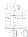
図1は本発明の実施形態に係るデータバス接続例を示すブロック図である。このシステムは、複数のモジュール1、モジュール2、…モジュールnが共通のデータバス10に接続された構造を有し、データバス10には当該データバス10を介したデータ送受信を制御するバスインターフェースとしてのDMA(Direct Memory Access)コントローラ12の他、CPU(中央演算処理装置)20、メモリコントローラ24及び外部デバイスコントローラ30が接続されている。なお、モジュール1〜nのみならず、CPU20及び外部デバイスコントローラ30もDMA要求を行う「モジュール」として扱うことができる。
【0017】
メモリコントローラ24はメモリ34に対するデータの読み書き動作を制御する。外部デバイスコントローラ30は、例えば、メモリカード、液晶ディスプレイなどの外部デバイス(図1中不図示)と接続され、外部デバイスへのデータ出力又は外部デバイスからのデータの読み込み制御等を行う。
【0018】
DMA要求を行うモジュール(1,2,…n,20,30)は、優先順位が定められており、DMAコントローラ12は、複数のモジュールからのDMA要求が競合した場合に、優先順位の最も高いモジュールのDMA要求に対して許可を与える。DMA要求に対する許可が与えられたモジュールは、データバス10を独占的に使用してメモリ34にアクセスし、データの読み書きを行う。
【0019】
本システムでは、各モジュール(1,2,…n,20,30)がDMA要求を出すことができるタイムスパン(要求許可期間)を管理するための手段としてシーケンサ40が設けられている。シーケンサ40には、各モジュール(1,2,…n,20,30)についてDMA要求を行うことができる期間が予め設定されている。それぞれのモジュールに与えられる要求許可期間は互いに重複しないタイミングで設定してもよいし、同じタイミングで複数のモジュールに要求許可期間を設定してもよい。
【0020】
要求許可期間が重複する設定においてDMA要求が競合した場合はDMAの優先順位に従って制御される。DMA要求許可期間の長さや許可を与える順序などの設定は適宜変更可能であり、各モジュールの処理内容や処理速度・優先順位等を考慮して適切な値に設定される。シーケンサ40は、その設定内容に従って各モジュール(1,2,…n,20,30)に対してDMA要求の出力を許可する信号を与える。
【0021】
各モジュール(1,2,…n,20,30)は、シーケンサ40から通告される要求許可期間内にDMA要求を出すことにより、必ずデータバス10を使用する機会が与えられる。したがって、優先順位が低いモジュールに対しても要求許可期間を適切に配分することによって、これら低順位モジュールも一定のタイミングでDMA転送を行うことが可能となり、システム全体の性能を向上させることができる。
【0022】
次に、上記の如く構成されたシステムの動作について説明する。説明を簡単にするために対象を簡略化し、モジュール1、モジュール2及びCPU20からDMA要求があった場合のデータバス10の使用例を説明する。なお、DMAの優先順位は、モジュール1>モジュール2>CPU20の順番とする。
【0023】
まず、比較のために、図2を用いて従来のバス制御方式によるデータバスの使用例を説明する。従来は「要求許可期間」という設定はなされておらず、単に優先順位に従ってデータバスを使用するモジュールが決定されていた。図2によれば、[1] のタイミングでモジュール1とCPUが同時にDMA要求を出す。[2] のタイミングで優先順位の高いモジュール1のDMA要求に対して許可が下りる。このときCPUは待ち状態となる。[3] のタイミングでモジュール2がDMA要求を出す。このとき、データバスはモジュール1によって使用中であるため、モジュール2は待ち状態となる。モジュール1がデータバスを使用している期間中に、モジュール1が[4] のタイミングで再度DMA要求を出している。[5] のタイミングでモジュール1のDMA転送(最初のDMA要求に係る転送処理)を終了するが、この時点で、モジュール1、モジュール2及びCPUがDMA要求を出しているので、[6] のタイミングで優先順位の高いモジュール1のDMA要求に対して再度許可が下り、モジュール2とCPUは待ち状態となる。
【0024】
[7] のタイミングでモジュール1のDMA転送が終了する。このとき、モジュール2とCPUがDMA要求を出しているが、[8] のタイミングで優先順位の高いモジュール2のDMA要求に対して許可が下り、CPUは待ち状態となる。モジュール2がデータバスを使用している期間中に、モジュール2が[9] のタイミングで再度DMA要求を出している。[10]のタイミングでモジュール2のDMA転送(最初のDMA要求に係る転送処理)を終了するが、この時点でモジュール2及びCPUがDMA要求を出しているので、[11]のタイミングで優先順位の高いモジュール2のDMA要求に対して再度許可が下り、CPUは待ち状態となる。
【0025】
[12] のタイミングでモジュール2のDMA転送が終了すると、この時点ではCPUのみがDMA要求を出している状態になるため、[13]のタイミングでCPUのDMAに対して許可が下りる。これにより、CPUがデータバスを使用する機会が与えられる。CPUがデータバスを使用して必要なデータ転送を実行し、[14]のタイミングでCPUのDMA転送が終了する。
【0026】
上記のように、従来の方式では、各モジュールからのDMA要求に対して、優先順位のみでDMAの許否が判断されるため、優先順位の低いモジュール(図2においてCPU)は、他の全ての上位モジュールがデータバスを使用していない場合にのみ、データバスの使用が許可されることになる。したがって、DMA転送を行うモジュールが増加するとシステム全体の性能を向上するのは困難であった。
【0027】
このような課題を解決すべく、本実施形態ではDMA要求を行うそれぞれのモジュールに対してDMA要求許可期間の設定を行うシーケンサ40を備えている。
【0028】
図3は、本発明の実施形態に係るバス制御方式によるデータバスの使用例である。同図によれば、シーケンサ40によって「モジュール1」→「CPU」→「モジュール2」→「モジュール1」→…という順番で循環式に要求許可期間が設定されている。モジュール1の要求許可期間内に[1] のタイミングでモジュール1がDMA要求を出す。[2] のタイミングでモジュール1のDMA要求に対して許可が下りる。モジュール1に許可が下りると、モジュール1がデータバス10を使用する。
【0029】
モジュール1の要求許可期間が終了し、続いてCPU20の要求許可期間となる。CPU20の要求許可期間内に[3] のタイミングでCPU20がDMA要求を出す。このとき、データバス10はモジュール1によって使用中であるため、CPU20は待ち状態となる。[4] のタイミングでモジュール1のDMA転送が終了すると、[5] のタイミングでCPU20のDMA要求に対して許可が下りる。こうして、CPU20によってデータバス10が使用される。
【0030】
CPU20の要求許可期間が終了するとモジュール2の要求許可期間となる。モジュール2の要求許可期間内に[6] のタイミングでモジュール2がDMA要求を出す。このとき、CPU20によってデータバス10が使用中であるため、モジュール2は待ち状態となる。やがて[7] のタイミングでCPU20のDMA転送が終了する。そして、[8] のタイミングでモジュール2のDMA要求に対して許可が下りる。これにより、モジュール2がデータバス10を使用する。
【0031】
また、モジュール2の要求許可期間終了後にモジュール1の要求許可期間となるが、当該モジュール1の要求許可期間内における[8] のタイミングでモジュール1がDMA要求を出す。しかし、このときデータバス10はモジュール2によって使用中であるため、モジュール1は待ち状態となる。
【0032】
[9] のタイミングでモジュール2のDMA転送が終了すると、[10]のタイミングでモジュール1のDMA要求に対して許可が下りる。これにより、モジュール1がデータバス10を使用する。
【0033】
モジュール1の要求許可期間終了後はCPU20の要求許可期間となるが、この期間内にCPU20がDMA要求を出さなかった場合、[11]のタイミングでモジュール2の要求許可期間に切り替わる。このモジュール2の要求許可期間中[12]のタイミングでモジュール1のDMA転送が終了すると同時に、モジュール2がDMA要求を出す。これにより、[13]のタイミングでモジュール2のDMA要求に許可が下り、モジュール2 がデータバス10を使用してデータ転送を実行する。その後、[14]のタイミングでモジュール2 のDMA転送が終了する。
【0034】
このように本実施形態によれば、各モジュールについて要求許可期間を設定し、シーケンサ40によって要求許可期間のサイクルを管理する構成にしたので、DMA要求の集中を回避してバスを効率良く使用できる。
【0035】
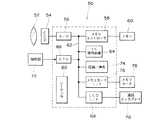
次に、本発明をデジタルカメラに適用した例を説明する。図4はデジタルカメラの構成を示すブロック図である。カメラ50は、撮影レンズ52の後方に撮像デバイスとしてのCCDイメージセンサ(以下、CCDという。)54を備えている。撮影レンズ52を介してCCD54の受光面に結像された被写体像は、CCD54の各フォトセンサ(感光画素)によって入射光量に応じた量の信号電荷に変換される。なお、CCD54は、シャッターゲートパルスのタイミングによって各フォトセンサの電荷蓄積時間(シャッタースピード)を制御する、いわゆる電子シャッター機能を有している。
【0036】
各フォトセンサに蓄積された信号電荷は、図示せぬCCDドライバから与えられるパルスに基づいて信号電荷に応じた電圧信号(画像信号)として順次読み出される。CCD54から出力された画像信号は、相関二重サンプリング(CDS)処理、色分離処理及び各色信号のゲイン調整等の所定のアナログ信号処理が施された後、A/D変換器56によりデジタル信号に変換される。デジタル信号に変換された画像信号は、メモリコントローラ58を介してメモリ60に格納される。
【0037】
メモリ60に格納されたデータは、データバス62を介して信号処理部64に送られる。信号処理部64は、輝度・色差(YC)信号生成回路、ガンマ補正回路、シャープネス補正回路、コントラスト補正回路、ホワイトバランス補正回路等を含むデジタルシグナルプロセッサ(DSP)で構成された画像処理手段であり、CPU66からのコマンドに従って画像信号を処理する。
【0038】
信号処理部64に入力された画像データは、輝度信号(Y信号)及び色差信号(Cr,Cb 信号)に変換されるとともに、ガンマ補正等の所定の処理が施された後、メモリ60に格納される。撮影画像を表示出力する場合、メモリ60から画像データが読み出され、表示用の所定方式の信号(例えば、NTSC方式のカラー複合映像信号)に変換された後、LCDインターフェース68を介して液晶ディスプレイ(LCD)70に出力される。こうして、当該画像データの画像内容が液晶ディスプレイ70に表示される。
【0039】
CCD54から出力される画像信号によってメモリ60内の画像データが定期的に書き換えられ、その画像データから生成される映像信号が液晶ディスプレイ70に供給されることにより、CCD54が撮像するリアルタイム画像(ムービー画像)が液晶ディスプレイ70に表示される。
【0040】
操作部72は、シャッターボタン、電源スイッチ、モード切換スイッチ、十字ボタンその他の各種操作スイッチを含むブロックである。カメラ50の制御部としてのCPU66は操作部72から受入する信号に基づき、対応する回路の動作を制御するとともに、液晶ディスプレイ70における表示の制御、ストロボ発光制御、オートフォーカス(AF)制御、自動露出(AE)制御、データ通信制御、及び記録処理の制御など撮影動作の制御を行う。すなわち、CPU66はシャッターボタンの「半押し」操作に応動して取り込んだ画像データから焦点評価演算やAE演算などの各種演算を行い、その演算結果に基づいてレンズ駆動部(不図示)を制御して撮影レンズ52を合焦位置に移動させる一方、絞り駆動部(不図示)を制御するとともに、CCD54の電荷蓄積時間を制御する。
【0041】
シャッターボタンが「全押し」操作されると、撮影開始指示(レリーズON)信号が発せられる。CPU66は、レリーズON信号の受け付けに応動して記録用の画像データの取り込みを開始するとともに、圧縮伸長回路74にコマンドを送る。これにより圧縮伸長回路74は、メモリ60に保持されている画像データをJPEGその他の所定の形式に従って圧縮する。
【0042】
圧縮された画像データは、メモリカードインターフェース76を介してメモリカード78記録される。記録媒体としては、スマートメディア、PCカード、コンパクトフラッシュ、磁気ディスク、光ディスク、光磁気ディスク、メモリスティックなど種々の形態を適用できる。使用される媒体に応じた信号処理手段とインターフェースが適用される。異種、同種の記録メディアを問わず、複数の媒体を装着可能な構成にしてもよい。また、画像を保存する手段は、リムーバブルメディアに限らず、カメラ50に内蔵された記録媒体(内蔵メモリ)であってもよい。内蔵メモリに画像を保存する態様の場合、データをパソコン等の外部機器に転送するための通信用インターフェースが設けられる。
【0043】
再生モード時には、メモリカード78から画像データが読み出され、読み出された画像データは、圧縮伸長回路74によって伸長処理された後、LCDインターフェース68を介して液晶ディスプレイ70に再生出力される。
【0044】
シーケンサ80は、DMA要求モジュールとしての信号処理部64、圧縮伸長回路74、メモリカードインターフェース76及びLCDインターフェース68の各回路ブロックの要求許可期間を管理する。
【0045】
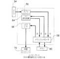
次に、上記の如く構成されたカメラ50における動作モード毎のデータの流れを説明する。図5は、ムービーモード(リアルタイム画像表示モード)におけるデータの流れを示している。ムービーモードでは、CCD54から出力された画像信号はA/D変換器56によってデジタル信号に変換され、このA/D変換出力がメモリコントローラ58を介してメモリ60に記憶される(符号▲1▼)。
【0046】
メモリ60に記憶されたデータは、メモリコントローラ58を介して読み出され、信号処理部64へ送られる(符号▲2▼)。信号処理部64は、読み込んだ画像データを基にYC変換処理、その他所定の信号処理を施す。所定の信号処理を経たデータは、メモリコントローラ58を介してメモリ60に書き戻される(符号▲3▼)。こうして、メモリ60に格納された画像データは、メモリコントローラ58を介して読み出され、LCDインターフェース68に送られる(符号▲4▼)。そして、表示用の映像信号に変換された後、液晶ディスプレイ70に供給される。
【0047】
図5に示した動作においてDMA優先順位は、A/D変換器56からのデータ取り込み▲1▼>信号処理部64へのデータ転送(YC処理のRead),信号処理部64からメモリ60へのデータ転送(YC処理のWrite )▲3▼>LCDインターフェース68へのデータ転送▲4▼の順に設定されている。なお、▲2▼と▲3▼は優劣無しとする。
【0048】
図6及び図7にはムービーモードにおける要求許可期間のタイミング(周期)の例が示されている。図6に示した〔例1〕は、各処理モジュールに対する要求許可期間を重複させずに順次処理を行う設定例である。すなわち、まずA/D変換器56に対して要求許可期間が与えられ、A/D変換出力をメモリ60に書き込む処理を行う。以下順次CPU→YC処理(Read) →CPU→YC処理(Write)→CPU→LCD→CPUの順に要求許可期間が切り替わり、再び先頭のA/Dに戻る。図6に示した通り、重複しない要求許可期間が循環式に切り替えられることにより、その順序に従って処理が進行する。
【0049】
図7に示した〔例2〕は、同タイミングで複数のモジュールに対して要求許可期間を与える例である。同図によれば、YC処理のReadとYC処理のWrite については重複的に要求許可期間が与えられる。重複タイミング時はDMAの優先順位に従って処理されるが、YC処理のReadとYC処理のWrite については必ず異なるタイミングで実施されるためDMA要求は競合しない。
【0050】
図8は記録用の静止画取り込みモードにおけるデータの流れを示している。取り込みモードでは、CCD54から出力された画像信号はA/D変換器56によってデジタル信号に変換され、このA/D変換出力がメモリコントローラ58を介してメモリ60に記憶される(符号▲1▼)。メモリ60に記憶されたデータは、メモリコントローラ58を介して読み出され、信号処理部64へ送られる(符号▲2▼)。信号処理部64は、読み込んだ画像データを基にYC変換処理その他所定の信号処理を施す。所定の信号処理を経たデータは、メモリコントローラ58を介してメモリ60に書き戻される(符号▲3▼)。
【0051】
こうして、メモリ60に格納された画像データは、メモリコントローラ58を介して読み出され、圧縮伸長回路74へ送られる(符号▲4▼)。圧縮伸長回路74において圧縮された画像データは、メモリコントローラ58を介して再びメモリ60に書き込まれる(符号▲5▼)。その後、圧縮データは、メモリコントローラ58を介してメモリ60から読み出され、メモリカードインターフェース76に送られる(符号▲6▼)。そして、メモリカードインターフェース76を介して圧縮画像データがメモリカード78に書き込まれる。
【0052】
図8に示した動作においてDMA優先順位は、A/D変換器56からのデータ取り込み▲1▼>信号処理部64へのデータ転送(YC処理Read)▲2▼,信号処理部64からメモリ60へのデータ転送(YC処理Write )▲3▼>圧縮伸長回路74へのデータ転送(圧縮Read)▲4▼,圧縮伸長回路74からメモリ60へのデータ転送(圧縮Write )▲5▼>メモリカードインターフェース76へのデータ転送▲6▼の順に設定されている。なお、▲2▼と▲3▼は優劣が無く、▲4▼と▲5▼も優劣は無いものとする。
【0053】
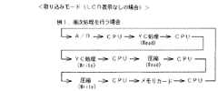
図9及び図10には取り込みモード(LCD表示なしの場合)における要求許可期間のタイミング(周期)の例が示されている。図9に示した〔例1〕は、各処理モジュールに対する要求許可期間を重複させずに順次処理を行う設定例である。図9に示した順序に従って要求許可期間が循環式に切り替わり、画像取り込みの処理が進行する。
【0054】
図10に示した〔例2〕は、同タイミングで複数のモジュールに対して要求許可期間を与える例である。同図によれば、YC処理Readと圧縮Read及びメモリカードインターフェースへの転送処理の三工程について同じタイミングで要求許可期間が与えられる。同様に、YC処理Write 、圧縮Write 及びメモリカードへの書き込み処理の三工程についても同じタイミングで要求許可期間が設定されている。DMA要求が競合した場合はDMAの優先順位に従って制御され、順位の高いモジュールに対して許可が下る。
【0055】
図11は再生モードにおけるデータの流れを示している。再生モードでは、メモリカード78に記録されている画像データがメモリカードインターフェース76を介して読み出される。この読み出されたデータ(圧縮データ)は、メモリコントローラ58を介してメモリ60に格納される(符号▲1▼)。次いで、メモリコントローラ58は、メモリ60内の圧縮データを読み出し、これを圧縮伸長回路74に転送する(符号▲2▼)。圧縮伸長回路74で伸長処理された画像データはメモリコントローラ58を介してメモリ60に送られる(符号▲3▼)。
【0056】
そして、メモリ60に記憶されたデータは、メモリコントローラ58を介して読み出され、LCDインターフェース68に送られる(符号▲4▼)。そして、表示用の映像信号に変換された後、液晶ディスプレイ70に供給される。
【0057】
図11に示した動作においてDMA優先順位は、カードインターフェース取り込み▲1▼>圧縮伸長回路74へのデータ転送(伸長Read)▲2▼,圧縮伸長回路74からメモリ60へのデータ転送(伸長Write )▲3▼>LCDインターフェース68へのデータ転送▲4▼の順に設定されている。なお、▲2▼と▲3▼は優劣が無いものとする。
【0058】
図12及び図13には再生モード(LCD表示優先の場合)における要求許可期間のタイミング(周期)の例が示されている。図12に示した〔例1〕は、各処理モジュールに対する要求許可期間を重複させずに順次処理を行う設定例である。図12に示した順序に従って要求許可期間が循環式に切り替わり、画像再生の処理が進行する。
【0059】
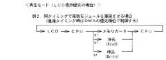
図13に示した〔例2〕は、同タイミングで複数のモジュールに対して要求許可期間を与える例である。同図によれば、メモリカードインターフェースからの取り込みと伸長Read及び伸長Write の各工程について同じタイミングで要求許可期間が与えられる。DMA要求が競合した場合はDMAの優先順位に基づいて制御される。
【0060】
図5乃至図13で説明したように、カメラ50の各動作モードに応じてDMA優先順位の設定並びに各モジュールの要求許可期間の設定が変更される。
【0061】
【発明の効果】
以上説明したように本発明によれば、複数のモジュールでデータバスを共有するシステムにおいて、各モジュールがDMA要求を出せるタイムスパン(要求許可期間)の設定を可能とする手段を設け、各モジュールが予め設定されたタイミングでDMA要求を出すようにしたので、DMA要求が時間的に分散され、バスレートを効率的に使用でき、システム全体の性能向上を図ることができる。
【図面の簡単な説明】
【図1】本発明の実施形態に係るデータバス接続例を示すブロック図
【図2】従来のバス制御方式によるデータバスの使用例を示すタイミングチャート
【図3】本発明の実施形態に係るバス制御方式によるデータバスの使用例を示すタイミングチャート
【図4】本発明を適用したデジタルカメラの構成を示すブロック図
【図5】図4に示したカメラのムービーモードにおけるデータの流れを示すブロック図
【図6】ムービーモードにおける要求許可期間の周期(例1)を示す図
【図7】ムービーモードにおける要求許可期間の周期(例2)を示す図
【図8】図4に示したカメラの取り込みモードにおけるデータの流れを示すブロック図
【図9】取り込みモードにおける要求許可期間の周期(例1)を示す図
【図10】取り込みモードにおける要求許可期間の周期(例2)を示す図
【図11】図4に示したカメラの再生モードにおけるデータの流れを示すブロック図
【図12】再生モードにおける要求許可期間の周期(例1)を示す図
【図13】再生モードにおける要求許可期間の周期(例2)を示す図
【符号の説明】
1…モジュール、2…モジュール、10…データバス、12…DMAコントローラ、20…CPU、24…メモリコントローラ、30…外部デバイスコントローラ、34…メモリ、40…シーケンサ、50…カメラ、54…CCD、56…A/D変換器、58…メモリコントローラ、60…メモリ、62…データバス、64…信号処理部、66…CPU、70…液晶ディスプレイ、74…圧縮伸長回路、76…メモリカードインターフェース、78…メモリカード、80…シーケンサ[0001]
BACKGROUND OF THE INVENTION
The present invention relates to a bus control method and apparatus and a digital camera, and more particularly to a bus control technique for effectively using the data bus in a system in which a plurality of modules share the same data bus.
[0002]
[Prior art]
Japanese Patent Laid-Open No. 7-141287 adopts an access method in which the CPU is directly involved in data transfer in order to avoid the occupation of resources generated by DMA transfer, and a slave controller that performs slave synchronization with the transfer operation of the CPU Is configured to perform DMA transfer from the I / O to the memory.
[0003]
In the data transfer control device disclosed in Japanese Patent Laid-Open No. 10-27155, a plurality of data processing units operating in parallel are connected to a single data bus, and the data transfer control unit transmits data to each data processing unit. The input / output is configured to execute in synchronization with the basic operation clock.
[0004]
The bus control device disclosed in Japanese Patent Application Laid-Open No. 11-272606 has a plurality of bus masters such as a processor and a DMA controller (DMAC), and when the processor transfers data to or from a memory or I / O, Each system bus control unit is configured to access the system bus in a minimum time width that can be accessed, and when the DMAC transfers data between the memory and the I / O, each system bus control The system bus is configured to be accessed in a minimum time width that can be accessed by the unit.
[0005]
[Problems to be solved by the invention]
As shown in the above publication, when DMA transfer is performed in a system in which a plurality of modules are connected to a common data bus, the DMAC arbitrates the DMA request from each module, and the DMA transfer is performed. DMA transfer is performed by giving a bus use permission (bus right) to a possible module. In this case, a module that issued a DMA request earlier or a module with a higher priority occupies the data bus continuously, and DMA transfer of other modules may not be possible.
[0006]
The present invention has been made in view of such circumstances, and enables a plurality of modules to share a data bus and perform DMA transfer efficiently, and a system that occurs when a specific module occupies the data bus. An object of the present invention is to provide a bus control method and apparatus capable of avoiding inconsistency of the above and a digital camera to which the bus control method and apparatus are applied.
[0007]
[Means for Solving the Problems]
In order to achieve the above object, the invention according to
[0008]
According to the present invention, a period during which a DMA request can be issued for each module (request permission period) is set in advance, and a DMA request cannot be issued from that module during a period other than the request permission period. The length of the request permission period (time span) and the period (or timing) for giving the request permission period can be appropriately set by the designer. Appropriate time span and request grant period are set in consideration of the system configuration and processing contents. If the request permission periods given to the modules do not overlap, the DMA request does not compete, so that each module can execute the DMA transfer in a fixed cycle. When request permission periods are given to two or more modules at the same timing, DMA request contention may occur. In this case, control is performed according to a predetermined DMA priority order.
[0009]
As described above, in the present invention, the time span for performing a DMA request is set for each module that performs a DMA request, and each module issues a DMA request at a predetermined timing. The DMA transfer can be performed without fail, and the performance of the entire system can be improved.
According to a second aspect of the present invention, in the bus control method according to the first aspect, the request permission period is given to some of the plurality of modules at the same grant timing. To do.
According to a third aspect of the present invention, in the bus control method according to thesecond aspect , when DMA requestsfrom a plurality of modules to which a request permission period is granted at thesame grant timing compete, a module having a higher priority The DMA transfer according to the DMA request from is permitted.
[0010]
In order to provide an apparatus that embodies the above-described method invention, a bus control device according to the invention described in
[0011]
The invention according to
According to a sixth aspect of the present invention, in the bus control device according to the fourth or fifth aspect, the request permission period is added to some of the plurality of modules at the same grant timing by the request permission period management means. It is characterized by giving.
According to a seventh aspect of the present invention, in the bus control device according to thesixth aspect, whenthe DMA requestsfrom a plurality of modules to which the request permission period is granted at thesame grant timing conflict, the request grant means It is characterized in that DMA transfer related to a DMA request from a module having a high priority is permitted.
[0012]
According to aneighth aspect of the present invention, the above-described bus control device is applied to a digital camera. The digital camera includes an imaging unit that converts an optical image into an electrical signal, and an image signal obtained from the imaging unit. A / D conversion means for converting the signal into a digital signal, signal processing means for converting the signal into a predetermined signal format based on the image signal output from the A / D conversion means, and the image signal temporarily according to the control of the DMA controller A memory for storing data, a compression processing means for compressing an image signal obtained by the signal processing means, a recording means for recording the compressed image signal on a recording medium, and a control means for controlling the operation of the camera body pressure in thea processing unit, the incorporation process of the image signal acquired through the a / D converting means, signal processing in the signal processing means, the compression processing unit Process, in relation to the processing of the recording processing and the processing unit by the recording means, a DMA transfer under the control of each of the requests permission period management means is characterized by being carried out.
[0013]
In addition to the above-described configuration, a digital camera according to aninth aspect of the present invention stores an expansion processing unit that expands a compressed image signal stored in the recording medium, an image acquired via the imaging unit, and the recording medium an image display unit capable of displaying an image being said anda display control means for outputting display signals to the image display means, image display of the decompression process and the image display means in the decompression processing unit With respect to processing, DMA transfer is performed under the management of the request permission period management means.
[0014]
The aspect of
[0015]
DETAILED DESCRIPTION OF THE INVENTION
Preferred embodiments of a bus control method and apparatus and a digital camera according to the present invention will be described below with reference to the accompanying drawings.
[0016]
FIG. 1 is a block diagram showing a data bus connection example according to an embodiment of the present invention. This system has a structure in which a plurality of
[0017]
The
[0018]
Modules (1, 2,... N, 20, 30) that perform DMA requests have priorities determined, and the
[0019]
In this system, a
[0020]
When DMA requests compete in a setting where request permission periods overlap, control is performed according to the priority of DMA. Settings such as the length of the DMA request permission period and the order in which permission is given can be changed as appropriate, and are set to appropriate values in consideration of the processing contents, processing speed, priority, etc. of each module. The
[0021]
Each module (1, 2,... N, 20, 30) is always given an opportunity to use the
[0022]
Next, the operation of the system configured as described above will be described. In order to simplify the description, the object is simplified, and an example of using the
[0023]
First, for comparison, an example of using a data bus according to a conventional bus control system will be described with reference to FIG. Conventionally, the setting of “request permission period” has not been made, and a module that uses a data bus is simply determined in accordance with the priority order. According to FIG. 2, the
[0024]
The DMA transfer of
[0025]
When the DMA transfer of the
[0026]
As described above, according to the conventional method, whether or not DMA is permitted is determined only by the priority order with respect to the DMA request from each module. Therefore, the module having a low priority order (CPU in FIG. 2) The use of the data bus is permitted only when the upper module does not use the data bus. Therefore, it is difficult to improve the performance of the entire system as the number of modules that perform DMA transfer increases.
[0027]
In order to solve such a problem, the present embodiment includes a
[0028]
FIG. 3 is a usage example of the data bus according to the bus control system according to the embodiment of the present invention. According to the figure, the request permission periods are set in a cyclic manner by the
[0029]
The request permission period for
[0030]
When the request permission period of the
[0031]
Also, after the request permission period of
[0032]
When the DMA transfer of
[0033]
After the request permission period of
[0034]
As described above, according to the present embodiment, since the request permission period is set for each module and the cycle of the request permission period is managed by the
[0035]
Next, an example in which the present invention is applied to a digital camera will be described. FIG. 4 is a block diagram showing the configuration of the digital camera. The
[0036]
The signal charge accumulated in each photosensor is sequentially read out as a voltage signal (image signal) corresponding to the signal charge based on a pulse supplied from a CCD driver (not shown). The image signal output from the
[0037]
The data stored in the
[0038]
The image data input to the
[0039]
The image data in the
[0040]
The
[0041]
When the shutter button is “fully pressed”, a shooting start instruction (release ON) signal is issued. In response to accepting the release ON signal, the
[0042]
The compressed image data is recorded on the
[0043]
In the playback mode, image data is read from the
[0044]
The
[0045]
Next, a data flow for each operation mode in the
[0046]
Data stored in the
[0047]
In the operation shown in FIG. 5, the DMA priority order is as follows: data acquisition from the A / D converter 56 {1}> data transfer to the signal processing unit 64 (Read of YC processing),
[0048]
6 and 7 show examples of timing (cycle) of the request permission period in the movie mode. [Example 1] illustrated in FIG. 6 is a setting example in which processing is sequentially performed without overlapping request permission periods for each processing module. That is, first, a request permission period is given to the A /
[0049]
[Example 2] shown in FIG. 7 is an example in which request permission periods are given to a plurality of modules at the same timing. According to the figure, the request permission period is given redundantly for the read of the YC process and the write of the YC process. At the time of duplication, processing is performed according to the priority of DMA, but DMA request does not compete because YC processing Read and YC processing Write are always executed at different timings.
[0050]
FIG. 8 shows a data flow in the still image capturing mode for recording. In the capture mode, the image signal output from the
[0051]
Thus, the image data stored in the
[0052]
In the operation shown in FIG. 8, the DMA priority order is as follows: data fetch from the A / D converter 56 (1)> data transfer to the signal processor 64 (YC process Read) (2),
[0053]
FIG. 9 and FIG. 10 show examples of timings (cycles) of the request permission period in the capture mode (when there is no LCD display). [Example 1] illustrated in FIG. 9 is a setting example in which processing is sequentially performed without overlapping request permission periods for each processing module. According to the order shown in FIG. 9, the request permission period is switched to a cyclic type, and the image capturing process proceeds.
[0054]
[Example 2] shown in FIG. 10 is an example in which request permission periods are given to a plurality of modules at the same timing. According to the figure, the request permission period is given at the same timing for the three steps of YC processing Read, compression Read, and transfer processing to the memory card interface. Similarly, the request permission period is set at the same timing for the three steps of YC processing Write, compression writing, and memory card writing processing. When a DMA request conflicts, control is performed according to the priority of DMA, and permission is given to a module having a higher order.
[0055]
FIG. 11 shows the data flow in the playback mode. In the reproduction mode, the image data recorded on the
[0056]
The data stored in the
[0057]
In the operation shown in FIG. 11, the DMA priority order is as follows: card interface capture (1)> data transfer to the compression / decompression circuit 74 (decompression Read) (2), data transfer from the compression /
[0058]
12 and 13 show examples of timing (period) of the request permission period in the reproduction mode (in the case of LCD display priority). [Example 1] shown in FIG. 12 is a setting example in which processing is sequentially performed without overlapping request permission periods for each processing module. According to the order shown in FIG. 12, the request permission period is switched to a cyclic type, and the image reproduction process proceeds.
[0059]
[Example 2] shown in FIG. 13 is an example in which request permission periods are given to a plurality of modules at the same timing. According to the figure, a request permission period is given at the same timing for each process of fetching from the memory card interface and decompression Read and decompression Write. When DMA requests conflict, control is performed based on the priority of DMA.
[0060]
As described with reference to FIGS. 5 to 13, the setting of the DMA priority order and the setting of the request permission period of each module are changed according to each operation mode of the
[0061]
【The invention's effect】
As described above, according to the present invention, in a system in which a data bus is shared by a plurality of modules, a means for enabling setting of a time span (request permission period) in which each module can issue a DMA request is provided. Since the DMA request is issued at a preset timing, the DMA request is temporally distributed, the bus rate can be used efficiently, and the performance of the entire system can be improved.
[Brief description of the drawings]
FIG. 1 is a block diagram showing an example of data bus connection according to an embodiment of the present invention. FIG. 2 is a timing chart showing an example of use of a data bus according to a conventional bus control system. FIG. 4 is a block diagram showing a configuration of a digital camera to which the present invention is applied. FIG. 5 is a block diagram showing a data flow in the movie mode of the camera shown in FIG. 6 is a diagram showing a cycle (example 1) of a request permission period in the movie mode. FIG. 7 is a diagram showing a cycle (example 2) of a request permission period in the movie mode. FIG. 9 is a block diagram showing the flow of data in the mode. FIG. 9 is a diagram showing a cycle of the request permission period in the capture mode (Example 1). FIG. 11 is a block diagram showing the flow of data in the playback mode of the camera shown in FIG. 4. FIG. 12 is a diagram showing the cycle of request permission period (example 1) in the playback mode. FIG. 13 is a diagram showing a period of request permission period (example 2) in the reproduction mode.
DESCRIPTION OF
Claims (10)
Translated fromJapanese前記複数のモジュールが前記データバスに接続されて構成されるデータ転送システムの構成及び処理の内容に応じて各モジュールに対して設定された、各モジュールがDMA要求を出すことができる要求許可期間のタイムスパンと、前記データ転送システムの構成及び処理の内容に応じて、各モジュールに対して所定の周期で要求許可期間が与えられるように設定された前記要求許可期間の付与タイミングとに従って各モジュールの要求許可期間を管理し、
前記管理の下で各モジュールが要求許可期間内にDMA要求を出すようにし、
第1のモジュールがDMA要求を出したときに、前記データバスが前記複数のモジュールのうちの前記第1のモジュール以外のモジュールのうちのいずれかによって使用中でない場合には、前記第1のモジュールがDMA要求を出し次第、該DMA要求に係るDMA転送を許可する一方、第1のモジュールが要求許可期間内にDMA要求を出したときに、前記データバスが前記複数のモジュールのうちの前記第1のモジュール以外の第2のモジュールによって使用中の場合には、前記第1のモジュールを待ち状態とし、
前記第2のモジュールによるDMA転送が終了した後に、前記待ち状態とした第1のモジュールのDMA要求に係るDMA転送を許可することを特徴とするバス制御方法。A data transfer system bus control method in which a plurality of modules performing a DMA request perform a DMA transfer using the same data bus,
A request permission period set for each module according to the configuration of the data transfer system configured by connecting the plurality of modules to the data bus and the content of the processing, so that each module can issue a DMA request. According to the time span and the grant timing of the request permission period set so that the request permission period is given to each module in a predetermined cycle according to the configuration and processing contents of the data transfer system . Manage the request grant period,
Under the management, each module issues a DMA request within the request grant period,
If the data bus is not in use byany of the plurality of modules other than the first modulewhen the first module issues a DMA request , the first module There soon issue a DMA request, while allowing DMA transfer according to the DMA request,when the first module issues a DMA request in the request permission period,the first of the data busof the plurality of modules byone of the secondmodules except when inuse, a state waiting for the first module,
A bus control method for permitting DMA transfer related to the DMA request of the first module in the waiting state after DMA transfer by the second module is completed.
前記複数のモジュールが接続されている共通のデータバスと、
各モジュールから出されるDMA要求を調停し、DMA転送可能なモジュールに対して前記データバスの使用許可を与え、当該モジュールによるDMA転送の実施を制御するDMAコントローラと、
各モジュールがDMA要求を出すことができる要求許可期間を管理する要求許可期間管理手段であって、前記複数のモジュールが前記データバスに接続されて構成されるデータ転送システムの構成及び処理の内容に応じて、各モジュールに対して設定された前記要求許可期間のタイムスパンと、前記データ転送システムの構成及び処理の内容に応じて、各モジュールに対して所定の周期で要求許可期間が与えられるように設定された前記要求許可期間の付与タイミングとに従って、各モジュールの要求許可期間を管理し、各モジュールに対して要求許可期間を示す信号を与える要求許可期間管理手段と、
第1のモジュールがDMA要求を出したときに、前記データバスが前記複数のモジュールのうちの前記第1のモジュール以外のモジュールのうちのいずれかによって使用中でない場合には、前記第1のモジュールがDMA要求を出し次第、該DMA要求に係るDMA転送を許可する一方、第1のモジュールが要求許可期間内にDMA要求を出したときに、前記データバスが前記複数のモジュールのうちの前記第1のモジュール以外の第2のモジュールによって使用中の場合には、前記第1のモジュールを待ち状態とし、前記第2のモジュールによるDMA転送が終了した後に、前記待ち状態とした第1のモジュールのDMA要求に係るDMA転送を許可する要求許可手段と、
を備えたことを特徴とするバス制御装置。A plurality of modules that perform DMA requests;
A common data bus to which the plurality of modules are connected;
A DMA controller that arbitrates a DMA request issued from each module, gives a permission to use the data bus to a module capable of DMA transfer, and controls execution of DMA transfer by the module;
Request permission period management means for managing a request permission period during which each module can issue a DMA request, wherein the plurality of modules are connected to the data bus, and the configuration and processing contents of the data transfer system are configured. Accordingly, the request permission period is given to each module at a predetermined cycle according to the time span of the request permission period set for each module and the configuration and processing contents of the data transfer system. Request permission period management means for managing the request permission period of each module in accordance with therequest permission period grant timing set in (1 ) and giving a signal indicating the request permission period to each module;
If the data bus is not in use byany of the plurality of modules other than the first modulewhen the first module issues a DMA request , the first module When the first module issues a DMA request, the data bus permits the DMA transfer according to the DMA request, while the first bus issues a DMA request within the requestgrant period, the data bus is the first of theplurality of modules. when in use byone of the second moduleexceptmodule, a state waiting for the first module, after the DMA transfer is completed by the second module, the first module and the waiting state Request permitting means for permitting DMA transfer according to the DMA request;
A bus control device comprising:
光学像を電気信号に変換する撮像手段と、
前記撮像手段から得られた画像信号をデジタル信号に変換するA/D変換手段と、
前記A/D変換手段から出力された画像信号を基に所定の信号形式に変換する信号処理手段と、
前記DMAコントローラの制御に従って画像信号を一時的に記憶するメモリと、
前記信号処理手段で得た画像信号を圧縮する圧縮処理手段と、
前記圧縮された画像信号を記録媒体に記録する記録手段と、
カメラ本体の動作を制御する制御手段としての演算処理装置とを備え、
前記A/D変換手段を介して取得される画像信号の取り込み処理、前記信号処理手段における信号処理、前記圧縮処理手段における圧縮処理、前記記録手段による記録処理及び前記演算処理装置の処理に関して、それぞれ前記要求許可期間管理手段の管理の下でDMA転送が実施されることを特徴とするデジタルカメラ。A digital camera equipped with the bus control device according to any one of claims 4 to 7, wherein the digital camera includes:
Imaging means for converting an optical image into an electrical signal;
A / D conversion means for converting an image signal obtained from the imaging means into a digital signal;
Signal processing means for converting to a predetermined signal format based on the image signal output from the A / D conversion means;
A memory for temporarily storing image signals according to the control of the DMA controller;
Compression processing means for compressing the image signal obtained by the signal processing means;
Recording means for recording the compressed image signal on a recording medium;
An arithmetic processing unit as a control means for controlling the operation of the camera body,
Regarding image signal acquisition processing acquired via the A / D conversion means, signal processing in the signal processing means, compression processing in the compression processing means, recording processing by the recording means, and processing of the arithmetic processing unit, respectively A digital camera, wherein DMA transfer is performed under the control of the request permission period management means.
前記撮像手段を介して取得した画像及び前記記録媒体に格納されている画像を表示可能な画像表示手段と、
前記画像表示手段に対して表示用の信号を出力する表示制御手段とを備え、
前記伸長処理手段における伸長処理並びに前記画像表示手段への画像表示処理に関して、それぞれ前記要求許可期間管理手段の管理の下でDMA転送が実施されることを特徴とする請求項8記載のデジタルカメラ。Decompression processing means for decompressing a compressed image signal stored in the recording medium;
Image display means capable of displaying an image acquired via the imaging means and an image stored in the recording medium;
Display control means for outputting a display signal to the image display means,
9. The digital camera according to claim 8, wherein DMA transfer is performed under the management of the request permission period management unit with respect to the decompression processing in the decompression processing unit and the image display processing on the image display unit.
Priority Applications (1)
| Application Number | Priority Date | Filing Date | Title |
|---|---|---|---|
| JP2001323375AJP4328906B2 (en) | 2001-10-22 | 2001-10-22 | Bus control method and apparatus, and digital camera |
Applications Claiming Priority (1)
| Application Number | Priority Date | Filing Date | Title |
|---|---|---|---|
| JP2001323375AJP4328906B2 (en) | 2001-10-22 | 2001-10-22 | Bus control method and apparatus, and digital camera |
Publications (2)
| Publication Number | Publication Date |
|---|---|
| JP2003132007A JP2003132007A (en) | 2003-05-09 |
| JP4328906B2true JP4328906B2 (en) | 2009-09-09 |
Family
ID=19140272
Family Applications (1)
| Application Number | Title | Priority Date | Filing Date |
|---|---|---|---|
| JP2001323375AExpired - Fee RelatedJP4328906B2 (en) | 2001-10-22 | 2001-10-22 | Bus control method and apparatus, and digital camera |
Country Status (1)
| Country | Link |
|---|---|
| JP (1) | JP4328906B2 (en) |
Families Citing this family (10)
| Publication number | Priority date | Publication date | Assignee | Title |
|---|---|---|---|---|
| JP2005078161A (en)* | 2003-08-28 | 2005-03-24 | Canon Inc | Recording device |
| JP2006039672A (en)* | 2004-07-22 | 2006-02-09 | Olympus Corp | Bus request control circuit |
| JP4792766B2 (en)* | 2005-02-25 | 2011-10-12 | カシオ計算機株式会社 | Data transfer device and imaging device |
| JP5224492B2 (en)* | 2005-12-16 | 2013-07-03 | カシオ計算機株式会社 | Image data transfer control device, image data transfer method, and camera having the image data transfer device |
| JP5125890B2 (en)* | 2008-08-28 | 2013-01-23 | 富士通セミコンダクター株式会社 | Arbitration device and electronic device |
| CN101673252B (en)* | 2008-09-08 | 2012-05-23 | 安辰电脑股份有限公司 | Dma system |
| WO2013015052A1 (en) | 2011-07-28 | 2013-01-31 | 富士フイルム株式会社 | Camera control system and method of controlling operation thereof |
| JP5891769B2 (en)* | 2011-12-19 | 2016-03-23 | 株式会社リコー | Image forming apparatus and image forming method |
| JP2016151949A (en)* | 2015-02-18 | 2016-08-22 | ファナック株式会社 | Dma controller |
| JP6556022B2 (en) | 2015-10-30 | 2019-08-07 | キヤノン株式会社 | Image processing apparatus and image processing method |
- 2001
- 2001-10-22JPJP2001323375Apatent/JP4328906B2/ennot_activeExpired - Fee Related
Also Published As
| Publication number | Publication date |
|---|---|
| JP2003132007A (en) | 2003-05-09 |
Similar Documents
| Publication | Publication Date | Title |
|---|---|---|
| US6963374B2 (en) | Method for live view display and digital camera using same | |
| US7573504B2 (en) | Image recording apparatus, image recording method, and image compressing apparatus processing moving or still images | |
| JP3720268B2 (en) | Image processing device | |
| US7365777B2 (en) | Digital camera | |
| JP4328906B2 (en) | Bus control method and apparatus, and digital camera | |
| US20110193988A1 (en) | Semiconductor device and semiconductor integrated circuit | |
| US9363440B2 (en) | Imaging device and imaging method that sets a phase difference between first and second synchronization signals | |
| WO2020170729A1 (en) | Image-capturing element, image-capturing device, image-capturing element operation method, and program | |
| JP4284458B2 (en) | Digital camera | |
| JP3806698B2 (en) | Electronic camera | |
| JP4298358B2 (en) | Image processing system | |
| US20030043291A1 (en) | Digital camera apparatus | |
| JP2013211724A (en) | Imaging apparatus | |
| JP2013211715A (en) | Imaging device | |
| JP4487454B2 (en) | Electronic camera and control IC for electronic camera | |
| JP6447595B2 (en) | Control device, process execution device, control method, process execution method, and control system | |
| JP2021082878A (en) | Imaging device | |
| JP3962440B2 (en) | Image processing device | |
| JP3858447B2 (en) | Electronic camera device | |
| KR20000017456A (en) | Video signal processing circuit and image pickup apparatususing the circuit | |
| US11314664B2 (en) | Memory access device, image processing device and imaging device | |
| JP4069000B2 (en) | Digital camera | |
| JP2000316121A (en) | Multiple access mode picture buffer | |
| JP4677581B2 (en) | Data transfer control device and data transfer method | |
| Kao et al. | Reusable embedded software platform for versatile single-sensor digital cameras |
Legal Events
| Date | Code | Title | Description |
|---|---|---|---|
| A621 | Written request for application examination | Free format text:JAPANESE INTERMEDIATE CODE: A621 Effective date:20040227 | |
| A977 | Report on retrieval | Free format text:JAPANESE INTERMEDIATE CODE: A971007 Effective date:20060811 | |
| A131 | Notification of reasons for refusal | Free format text:JAPANESE INTERMEDIATE CODE: A131 Effective date:20060829 | |
| A521 | Request for written amendment filed | Free format text:JAPANESE INTERMEDIATE CODE: A523 Effective date:20061030 | |
| A711 | Notification of change in applicant | Free format text:JAPANESE INTERMEDIATE CODE: A712 Effective date:20061204 | |
| A131 | Notification of reasons for refusal | Free format text:JAPANESE INTERMEDIATE CODE: A131 Effective date:20070705 | |
| A521 | Request for written amendment filed | Free format text:JAPANESE INTERMEDIATE CODE: A523 Effective date:20070903 | |
| A131 | Notification of reasons for refusal | Free format text:JAPANESE INTERMEDIATE CODE: A131 Effective date:20080604 | |
| A521 | Request for written amendment filed | Free format text:JAPANESE INTERMEDIATE CODE: A523 Effective date:20080801 | |
| TRDD | Decision of grant or rejection written | ||
| A01 | Written decision to grant a patent or to grant a registration (utility model) | Free format text:JAPANESE INTERMEDIATE CODE: A01 Effective date:20090519 | |
| A01 | Written decision to grant a patent or to grant a registration (utility model) | Free format text:JAPANESE INTERMEDIATE CODE: A01 | |
| A61 | First payment of annual fees (during grant procedure) | Free format text:JAPANESE INTERMEDIATE CODE: A61 Effective date:20090601 | |
| R150 | Certificate of patent or registration of utility model | Free format text:JAPANESE INTERMEDIATE CODE: R150 | |
| FPAY | Renewal fee payment (event date is renewal date of database) | Free format text:PAYMENT UNTIL: 20120626 Year of fee payment:3 | |
| FPAY | Renewal fee payment (event date is renewal date of database) | Free format text:PAYMENT UNTIL: 20120626 Year of fee payment:3 | |
| FPAY | Renewal fee payment (event date is renewal date of database) | Free format text:PAYMENT UNTIL: 20130626 Year of fee payment:4 | |
| R250 | Receipt of annual fees | Free format text:JAPANESE INTERMEDIATE CODE: R250 | |
| R250 | Receipt of annual fees | Free format text:JAPANESE INTERMEDIATE CODE: R250 | |
| R250 | Receipt of annual fees | Free format text:JAPANESE INTERMEDIATE CODE: R250 | |
| R250 | Receipt of annual fees | Free format text:JAPANESE INTERMEDIATE CODE: R250 | |
| LAPS | Cancellation because of no payment of annual fees |