JP4326604B2 - Method for manufacturing semiconductor device - Google Patents
Method for manufacturing semiconductor deviceDownload PDFInfo
- Publication number
- JP4326604B2 JP4326604B2JP28255997AJP28255997AJP4326604B2JP 4326604 B2JP4326604 B2JP 4326604B2JP 28255997 AJP28255997 AJP 28255997AJP 28255997 AJP28255997 AJP 28255997AJP 4326604 B2JP4326604 B2JP 4326604B2
- Authority
- JP
- Japan
- Prior art keywords
- electrode
- film
- semiconductor
- crystal structure
- layer
- Prior art date
- Legal status (The legal status is an assumption and is not a legal conclusion. Google has not performed a legal analysis and makes no representation as to the accuracy of the status listed.)
- Expired - Fee Related
Links
- 239000004065semiconductorSubstances0.000titleclaimsdescription160
- 238000000034methodMethods0.000titleclaimsdescription73
- 238000004519manufacturing processMethods0.000titleclaimsdescription46
- 239000010408filmSubstances0.000claimsdescription240
- 239000003990capacitorSubstances0.000claimsdescription84
- 230000015572biosynthetic processEffects0.000claimsdescription51
- 239000013078crystalSubstances0.000claimsdescription33
- 239000010409thin filmSubstances0.000claimsdescription30
- 239000012535impuritySubstances0.000claimsdescription29
- 230000003197catalytic effectEffects0.000claimsdescription24
- 238000005530etchingMethods0.000claimsdescription24
- 238000010438heat treatmentMethods0.000claimsdescription24
- 238000000059patterningMethods0.000claimsdescription24
- 239000000758substrateSubstances0.000claimsdescription21
- 238000002425crystallisationMethods0.000claimsdescription14
- 230000008025crystallizationEffects0.000claimsdescription14
- 238000000137annealingMethods0.000claimsdescription9
- 230000001737promoting effectEffects0.000claimsdescription6
- OFIYHXOOOISSDN-UHFFFAOYSA-NtellanylidenegalliumChemical compound[Te]=[Ga]OFIYHXOOOISSDN-UHFFFAOYSA-N0.000claimsdescription5
- 239000010410layerSubstances0.000description230
- 239000011159matrix materialSubstances0.000description31
- 230000008569processEffects0.000description30
- OAICVXFJPJFONN-UHFFFAOYSA-NPhosphorusChemical compound[P]OAICVXFJPJFONN-UHFFFAOYSA-N0.000description27
- 229910052581Si3N4Inorganic materials0.000description27
- 238000005247getteringMethods0.000description27
- HQVNEWCFYHHQES-UHFFFAOYSA-Nsilicon nitrideChemical compoundN12[Si]34N5[Si]62N3[Si]51N64HQVNEWCFYHHQES-UHFFFAOYSA-N0.000description27
- 229910052698phosphorusInorganic materials0.000description26
- 239000011574phosphorusSubstances0.000description26
- PXHVJJICTQNCMI-UHFFFAOYSA-NNickelChemical compound[Ni]PXHVJJICTQNCMI-UHFFFAOYSA-N0.000description23
- 230000001681protective effectEffects0.000description17
- ZOXJGFHDIHLPTG-UHFFFAOYSA-NBoronChemical compound[B]ZOXJGFHDIHLPTG-UHFFFAOYSA-N0.000description16
- 229910052796boronInorganic materials0.000description16
- 229910052710siliconInorganic materials0.000description16
- XUIMIQQOPSSXEZ-UHFFFAOYSA-NSiliconChemical compound[Si]XUIMIQQOPSSXEZ-UHFFFAOYSA-N0.000description15
- 229910021417amorphous siliconInorganic materials0.000description15
- 239000010703siliconSubstances0.000description15
- VYPSYNLAJGMNEJ-UHFFFAOYSA-Nsilicon dioxideInorganic materialsO=[Si]=OVYPSYNLAJGMNEJ-UHFFFAOYSA-N0.000description14
- 229910052814silicon oxideInorganic materials0.000description11
- 229910021419crystalline siliconInorganic materials0.000description10
- 230000000694effectsEffects0.000description10
- 150000002500ionsChemical class0.000description10
- 239000011229interlayerSubstances0.000description9
- 230000005684electric fieldEffects0.000description8
- 238000005468ion implantationMethods0.000description7
- 229910021420polycrystalline siliconInorganic materials0.000description7
- XYFCBTPGUUZFHI-UHFFFAOYSA-NPhosphineChemical compoundPXYFCBTPGUUZFHI-UHFFFAOYSA-N0.000description6
- 230000015556catabolic processEffects0.000description6
- 239000007789gasSubstances0.000description6
- 229910052759nickelInorganic materials0.000description6
- 230000007423decreaseEffects0.000description5
- 239000011521glassSubstances0.000description5
- 229910052751metalInorganic materials0.000description5
- 239000002184metalSubstances0.000description5
- 239000010936titaniumSubstances0.000description5
- IJGRMHOSHXDMSA-UHFFFAOYSA-NAtomic nitrogenChemical compoundN#NIJGRMHOSHXDMSA-UHFFFAOYSA-N0.000description4
- 239000000969carrierSubstances0.000description4
- 229910052732germaniumInorganic materials0.000description4
- 239000004973liquid crystal related substanceSubstances0.000description4
- 230000004048modificationEffects0.000description4
- 238000012986modificationMethods0.000description4
- KDLHZDBZIXYQEI-UHFFFAOYSA-NPalladiumChemical compound[Pd]KDLHZDBZIXYQEI-UHFFFAOYSA-N0.000description3
- 239000011248coating agentSubstances0.000description3
- 238000000576coating methodMethods0.000description3
- 239000000470constituentSubstances0.000description3
- 238000013461designMethods0.000description3
- 230000006866deteriorationEffects0.000description3
- 238000010586diagramMethods0.000description3
- 238000009792diffusion processMethods0.000description3
- GNPVGFCGXDBREM-UHFFFAOYSA-Ngermanium atomChemical compound[Ge]GNPVGFCGXDBREM-UHFFFAOYSA-N0.000description3
- 230000006872improvementEffects0.000description3
- 229910000073phosphorus hydrideInorganic materials0.000description3
- 238000009832plasma treatmentMethods0.000description3
- BASFCYQUMIYNBI-UHFFFAOYSA-NplatinumChemical compound[Pt]BASFCYQUMIYNBI-UHFFFAOYSA-N0.000description3
- 239000010453quartzSubstances0.000description3
- 230000009467reductionEffects0.000description3
- OKTJSMMVPCPJKN-UHFFFAOYSA-NCarbonChemical compound[C]OKTJSMMVPCPJKN-UHFFFAOYSA-N0.000description2
- GYHNNYVSQQEPJS-UHFFFAOYSA-NGalliumChemical compound[Ga]GYHNNYVSQQEPJS-UHFFFAOYSA-N0.000description2
- 239000004642PolyimideSubstances0.000description2
- 230000001133accelerationEffects0.000description2
- 238000001994activationMethods0.000description2
- 239000010407anodic oxideSubstances0.000description2
- 229910052787antimonyInorganic materials0.000description2
- WATWJIUSRGPENY-UHFFFAOYSA-Nantimony atomChemical compound[Sb]WATWJIUSRGPENY-UHFFFAOYSA-N0.000description2
- 229910052785arsenicInorganic materials0.000description2
- RQNWIZPPADIBDY-UHFFFAOYSA-Narsenic atomChemical compound[As]RQNWIZPPADIBDY-UHFFFAOYSA-N0.000description2
- QVGXLLKOCUKJST-UHFFFAOYSA-Natomic oxygenChemical compound[O]QVGXLLKOCUKJST-UHFFFAOYSA-N0.000description2
- 230000008901benefitEffects0.000description2
- 229910052799carbonInorganic materials0.000description2
- 239000003054catalystSubstances0.000description2
- 150000001875compoundsChemical class0.000description2
- 239000010949copperSubstances0.000description2
- 230000007547defectEffects0.000description2
- 229910052733galliumInorganic materials0.000description2
- 239000010931goldSubstances0.000description2
- 229910052736halogenInorganic materials0.000description2
- 150000002367halogensChemical class0.000description2
- 229910052738indiumInorganic materials0.000description2
- APFVFJFRJDLVQX-UHFFFAOYSA-Nindium atomChemical compound[In]APFVFJFRJDLVQX-UHFFFAOYSA-N0.000description2
- 238000002347injectionMethods0.000description2
- 239000007924injectionSubstances0.000description2
- 230000001678irradiating effectEffects0.000description2
- 229910052757nitrogenInorganic materials0.000description2
- 229910052760oxygenInorganic materials0.000description2
- 239000001301oxygenSubstances0.000description2
- 230000003071parasitic effectEffects0.000description2
- 230000002093peripheral effectEffects0.000description2
- 239000012071phaseSubstances0.000description2
- 229920001721polyimidePolymers0.000description2
- 229920005591polysiliconPolymers0.000description2
- 238000000926separation methodMethods0.000description2
- 238000010532solid phase synthesis reactionMethods0.000description2
- 238000003860storageMethods0.000description2
- 229910052715tantalumInorganic materials0.000description2
- GUVRBAGPIYLISA-UHFFFAOYSA-Ntantalum atomChemical compound[Ta]GUVRBAGPIYLISA-UHFFFAOYSA-N0.000description2
- 239000004925Acrylic resinSubstances0.000description1
- 229920000178Acrylic resinPolymers0.000description1
- 229930091051ArenineNatural products0.000description1
- 241001239379Calophysus macropterusSpecies0.000description1
- VYZAMTAEIAYCRO-UHFFFAOYSA-NChromiumChemical compound[Cr]VYZAMTAEIAYCRO-UHFFFAOYSA-N0.000description1
- RYGMFSIKBFXOCR-UHFFFAOYSA-NCopperChemical compound[Cu]RYGMFSIKBFXOCR-UHFFFAOYSA-N0.000description1
- XEEYBQQBJWHFJM-UHFFFAOYSA-NIronChemical compound[Fe]XEEYBQQBJWHFJM-UHFFFAOYSA-N0.000description1
- 229910016024MoTaInorganic materials0.000description1
- ZOKXTWBITQBERF-UHFFFAOYSA-NMolybdenumChemical compound[Mo]ZOKXTWBITQBERF-UHFFFAOYSA-N0.000description1
- 239000004952PolyamideSubstances0.000description1
- 229910020286SiOxNyInorganic materials0.000description1
- RTAQQCXQSZGOHL-UHFFFAOYSA-NTitaniumChemical compound[Ti]RTAQQCXQSZGOHL-UHFFFAOYSA-N0.000description1
- NIXOWILDQLNWCW-UHFFFAOYSA-Nacrylic acid groupChemical groupC(C=C)(=O)ONIXOWILDQLNWCW-UHFFFAOYSA-N0.000description1
- 230000004913activationEffects0.000description1
- 229910045601alloyInorganic materials0.000description1
- 239000000956alloySubstances0.000description1
- 150000001408amidesChemical class0.000description1
- 239000007864aqueous solutionSubstances0.000description1
- 238000005229chemical vapour depositionMethods0.000description1
- 229910052804chromiumInorganic materials0.000description1
- 239000011651chromiumSubstances0.000description1
- 229910017052cobaltInorganic materials0.000description1
- 239000010941cobaltSubstances0.000description1
- GUTLYIVDDKVIGB-UHFFFAOYSA-Ncobalt atomChemical compound[Co]GUTLYIVDDKVIGB-UHFFFAOYSA-N0.000description1
- 239000002131composite materialSubstances0.000description1
- 229910052802copperInorganic materials0.000description1
- 238000006356dehydrogenation reactionMethods0.000description1
- 238000011161developmentMethods0.000description1
- 239000003989dielectric materialSubstances0.000description1
- 238000001312dry etchingMethods0.000description1
- 238000004870electrical engineeringMethods0.000description1
- 238000007715excimer laser crystallizationMethods0.000description1
- 238000002474experimental methodMethods0.000description1
- 230000005669field effectEffects0.000description1
- PCHJSUWPFVWCPO-UHFFFAOYSA-NgoldChemical compound[Au]PCHJSUWPFVWCPO-UHFFFAOYSA-N0.000description1
- 229910052737goldInorganic materials0.000description1
- 239000003779heat-resistant materialSubstances0.000description1
- 238000007689inspectionMethods0.000description1
- 239000012212insulatorSubstances0.000description1
- 238000005224laser annealingMethods0.000description1
- 238000002789length controlMethods0.000description1
- 239000000463materialSubstances0.000description1
- 238000005259measurementMethods0.000description1
- 239000000203mixtureSubstances0.000description1
- 229910052750molybdenumInorganic materials0.000description1
- 239000011733molybdenumSubstances0.000description1
- FBMUYWXYWIZLNE-UHFFFAOYSA-Nnickel phosphideChemical compound[Ni]=P#[Ni]FBMUYWXYWIZLNE-UHFFFAOYSA-N0.000description1
- RUFLMLWJRZAWLJ-UHFFFAOYSA-Nnickel silicideChemical compound[Ni]=[Si]=[Ni]RUFLMLWJRZAWLJ-UHFFFAOYSA-N0.000description1
- 229910021334nickel silicideInorganic materials0.000description1
- 230000003287optical effectEffects0.000description1
- 230000001590oxidative effectEffects0.000description1
- 229910052763palladiumInorganic materials0.000description1
- 229910052697platinumInorganic materials0.000description1
- 229920002647polyamidePolymers0.000description1
- 239000011347resinSubstances0.000description1
- 229920005989resinPolymers0.000description1
- 238000005070samplingMethods0.000description1
- 239000000243solutionSubstances0.000description1
- 241000894007speciesSpecies0.000description1
- 238000004528spin coatingMethods0.000description1
- 238000004544sputter depositionMethods0.000description1
- MZLGASXMSKOWSE-UHFFFAOYSA-Ntantalum nitrideChemical compound[Ta]#NMZLGASXMSKOWSE-UHFFFAOYSA-N0.000description1
- 238000002230thermal chemical vapour depositionMethods0.000description1
- 229910052719titaniumInorganic materials0.000description1
- WFKWXMTUELFFGS-UHFFFAOYSA-NtungstenChemical compound[W]WFKWXMTUELFFGS-UHFFFAOYSA-N0.000description1
- 229910052721tungstenInorganic materials0.000description1
- 239000010937tungstenSubstances0.000description1
- 238000007740vapor depositionMethods0.000description1
- 239000012808vapor phaseSubstances0.000description1
- 229910052727yttriumInorganic materials0.000description1
Images


Landscapes
- Liquid Crystal (AREA)
- Recrystallisation Techniques (AREA)
- Shift Register Type Memory (AREA)
- Thin Film Transistor (AREA)
Description
Translated fromJapanese【0001】
【発明が属する技術分野】
本願発明は結晶構造を有する半導体薄膜を利用した半導体装置およびその作製方法に関する。特に、逆スタガ構造の薄膜トランジスタ(以下、TFTと略記する)を用いた半導体装置に関する。
【0002】
なお、本明細書中において「半導体装置」とは、半導体特性を利用して動作させる装置全てを指す。従って本明細書に記載されたTFT、AMLCD(アクティブマトリクス型液晶表示装置)及び電子機器は全て半導体装置の範疇に含むものとする。
【0003】
【従来の技術】
従来より、アクティブマトリクス型液晶表示装置(以下、AMLCDと略記する)のスイッチング素子としてTFTが利用されている。現在では非晶質珪素膜(アモルファスシリコン膜)を活性層として利用したTFTで回路構成を行う製品が市場を占めている。特に、TFT構造としては製造工程の簡単な逆スタガ構造が多く採用されている。
【0004】
しかし、年々AMLCDの高性能化が進み、TFTに求められる動作性能(特に動作速度)は厳しくなる傾向にある。そのため、非晶質珪素膜を用いたTFTの動作速度では十分な性能を有する素子を得ることが困難となった。
【0005】
そこで、非晶質珪素膜に代わって多結晶珪素膜(ポリシリコン膜)を利用したTFTが脚光を浴び、多結晶珪素膜を活性層とするTFTの開発が著しい勢いで進んできている。現在では、その一部で製品化も行われている。
【0006】
活性層として多結晶珪素膜を利用した逆スタガ型TFTの構造については既に多くの発表がなされている。例えば、「Fabrication of Low-Temperature Bottom-Gate Poly-Si TFTs on Large-Area Substrate by Linear-Beam Excimer Laser Crystallization and Ion Doping Method:H.Hayashi et.al.,IEDM95,PP829-832,1995」などの報告がある。
【0007】
同報告書では多結晶珪素膜を利用した逆スタガ構造の典型的な例(Fig.4 )を説明しているが、この様な構造の逆スタガ構造(いわゆるチャネルストップ型)では様々な問題も抱えている。
【0008】
まず、活性層全体が50nm程度と極めて薄いのでチャネル形成領域とドレイン領域との接合部において衝突電離(Impact Ionization )が発生し、ホットキャリア注入などの劣化現象が顕著に現れてしまう。そのため、大きなLDD領域(Light Doped Drain region)を形成する必要性が生じる。
【0009】
そして、このLDD領域の制御性が最も重大な問題となる。LDD領域は不純物濃度と領域の長さの制御が非常に微妙であり、特に長さ制御が問題となる。現状ではマスクパターンによってLDD領域の長さを規定する方式が採られているが、微細化が進めば僅かなパターニング誤差が大きなTFT特性の差を生む。
【0010】
活性層の膜厚のバラツキによるLDD領域のシート抵抗のバラツキも深刻な問題となる。さらに、ゲイト電極のテーパー角度等のバラツキもLDD領域の効果のバラツキを招く要因となりうる。
【0011】
また、LDD領域を形成するためにはパターニング工程が必要であり、それはそのまま製造工程の増加、スループットの低下を招く。上記報告書に記載された逆スタガ構造では、最低でもマスク6枚(ソース/ドレイン電極形成まで)が必要であると予想される。
【0012】
以上の様に、チャネルストップ型の逆スタガ構造ではチャネル形成領の両側に横方向の平面内でLDD領域を形成しなくてはならず、再現性あるLDD領域を形成することは非常に困難である。
【0013】
また、従来AMLCDでは液晶層に保持した電荷の漏れを補うため、補助容量を各画素に設ける構造となっている。
【0014】
【本発明が解決しようとする課題】
本願発明では、非常に簡易な製造工程によって、量産性が高く、且つ、信頼性及び再現性の高い半導体装置を作製する技術を提供することを課題とし、画素マトリクス回路に、TFTボトムゲイト型TFTと共に補助容量を作製する際に、工程を複雑化せずに、特にマスク数を増加することのなく作製可能な半導体装置の構成及びその作製方法を提供することにある。
【0015】
【課題を解決するための手段】
本明細書で開示する発明の構成は、複数のゲイト配線と、複数のソース配線と、各画素に配置されたボトムゲイト型薄膜トランジスタ及び画素電極に接続された補助容量とを有する画素マトリクス回路を備えた半導体装置であって、
前記薄膜トランジスタのソース領域と、ドレイン領域と、少なくとも1つのチャネル形成領域とが形成される薄膜半導体層は結晶構造を有し、
前記ソース領域及びドレイン領域は、ゲイト絶縁膜に向かって少なくとも第1の導電層、当該第1の導電層よりも高抵抗な第2の導電層及び前記チャネル形成領域と同一導電型の第1の半導体層からなる積層構造を有し、
前記第1及び第2の導電層に導電性を付与する不純物の濃度プロファイルは、前記第1の導電層から前記第2の導電層にかけて連続的に変化し、
前記補助容量は、ゲイト配線と同一の導電膜でなる第1の電極と、前記第1の電極に接する誘電体と、前記誘電体に接し、前記チャネル形成領域と同一導電型の第2の半導体層でなる第2の電極とを有することを特徴とする。
【0016】
また、他の発明の構成は、上記の構成を有する画素マトリクス回路において、補助容量の第2の電極に半導体層を用いる代わりに、前記ソース配線と共通の導電膜から形成することを特徴とする。
【0017】
また、他の発明の構成は、上記の構成を有する画素マトリクス回路において、画素電極と補助容量の第2の電極は前記ソース配線と共通の導電膜から形成することを特徴とする。
【0018】
また、他の発明の構成は、上記のマトリクス回路において、前記補助容量の一方の電極は前記ゲイト配線と共通の導電膜から形成され、前記画素電極は前記補助容量の誘電体と接する領域を有し、画素電極を補助容量の一方に電極に用いることを特徴とする半導体装置。
【0019】
また、作製方法に関する発明の構成は、
絶縁表面を有する基板上に、前記ゲイト配線、前記補助容量の第1の電極を形成する工程と、
前記ゲイト配線、前記第1の電極を覆う絶縁層を形成する工程と、
前記絶縁層上に非晶質半導体膜を形成する工程と、
前記非晶質半導体膜に対して結晶化を助長する触媒元素を添加し、加熱処理により結晶構造を有する半導体膜を得る工程と、
前記結晶構造を有する半導体膜に対して15族のみ或いは13族及び15族から選ばれた不純物を添加して、導電層を形成する工程と、
加熱処理により前記導電層に、前記結晶構造を有する半導体膜中の前記触媒元素をゲッタリングさせる工程と、
前記結晶構造を有する半導体膜をパターニングして、前記薄膜トランジスタのチャネル形成領域を構成する第1の薄膜半導体層と、前記絶縁層を介して前記第1の電極と重なる第2の薄膜半導体層とを形成する工程と、
前記ソース配線と、前記第1の薄膜半導体層上に薄膜トランジスタのソース領域、ドレイン領域が形成される領域を少なくとも覆う第1の導電膜と、前記第2の薄膜半導体層の表面を覆う第2の導電膜とを形成する工程と、
前記第1の導電膜をマスクとして、前記第1の薄膜半導体層をエッチングして、前記薄膜トランジスタのチャネル形成領域を形成する工程とを有し、
前記第2の薄膜半導体層には前記補助容量の第2の電極が形成されることを特徴とする。
【0020】
上記の作製方法によって、補助容量の一方の電極は半導体層に形成されるが、本発明の作製方法に関する他の構成は、前記ソース配線と、前記薄膜トランジスタのソース電極及びドレイン電極と共に、前記補助容量の第2の電極を形成して、ソース配線と共通の導電膜を補助容量の電極に用いる。
【0021】
さらに、他の方法では、前記画素電極を画素TFT及び補助容量の誘電体に接するように形成することで、画素電極を補助容量の電極に用いる。
【0022】
【発明の実施の形態】
以上の構成からなる本願発明の実施の形態について、以下に記載する実施例、特に実施例13以降において詳細な説明を行うこととする。
【0023】
【実施例】
以下、図1〜21を用いて本発明の実施例を詳細に説明する。
【0024】
〔実施例1〕 本願発明の代表的な実施例について、図1〜3を用いて説明する。まず、図1を用いて本願発明の半導体装置の作製方法を説明する。
【0025】
ガラス基板(または石英、シリコン基板)101上に珪素を主成分とする絶縁膜でなる下地膜102を形成する。その上に導電性膜でなるゲイト電極(第1配線)103を形成する。
【0026】
ゲイト電極103の線幅は1〜10μm(代表的には3〜5μm)とする。また、膜厚は 200〜500 nm(代表的には 250〜300 nm)とする。本実施例では 250nm厚のTa/TaN(タンタル/窒化タンタル)積層膜を用いて線幅3μmのゲイト電極を形成する。
【0027】
また、ゲイト電極103としては、少なくとも 600℃(好ましくは 800℃)の温度に耐えうる耐熱性を有する材料(タンタル、タングステン、チタン、クロム、モリブデン、導電性シリコン等)を用いる。その理由は後述する。ここで1回目のパターニング工程(ゲイト電極形成)が行われる。
【0028】
次に、窒化珪素膜104(膜厚は0〜200 nm、代表的には25〜100 nm、好ましくは50nm)、SiOx Ny で示される酸化窒化珪素膜又は酸化珪素膜(膜厚は 150〜300 nm、代表的には200 nm)105からなるゲイト絶縁層を形成し、その上に珪素を主成分とする非晶質半導体膜106を形成する。本実施例では非晶質珪素膜を例とするが他の化合物半導体膜(ゲルマニウムを含有する非晶質珪素膜等)を用いても良い。
【0029】
また、本願発明はチャネルエッチ型のボトムゲイト構造であるので、非晶質珪素膜106の膜厚は厚く形成しておく。膜厚範囲は 100〜600 nm(典型的には 200〜300 nm、好ましくは250 nm)とする。本実施例では200 nmとする。また、後述するが、最適な膜厚は本願発明のTFTにどの様なオフセット領域、LDD領域を設けるかによって適宜決定する必要がある。
【0030】
なお、本実施例では減圧熱CVD法により非晶質珪素膜106を成膜するが、成膜の際に炭素、酸素、窒素といった不純物の濃度を徹底的に管理することが望ましい。これらの不純物が多いと後の結晶化を阻害する恐れがある。
【0031】
本実施例では成膜した非晶質珪素膜中における各不純物の濃度が、炭素及び窒素が 5×10¹⁸atoms/cm3 未満(代表的には 5×10¹⁷atoms/cm3 以下)、酸素が 1.5×10¹⁹atoms/cm3 未満(代表的には 1×10¹⁸atoms/cm3 以下)となる様に制御する。この様な管理を行っておけば最終的にTFTのチャネル形成領域中に含まれる不純物濃度は上記範囲内に収まる。
【0032】
こうして図1(A)の状態が得られる。その次に、珪素の結晶化を助長する触媒元素(代表的にはニッケル)を含んだ溶液をスピンコート法により塗布し、Ni(ニッケル)含有層107を形成する。詳細な条件は本発明者らによる特開平7-130652号公報記載の技術(ここでは同公報の実施例1)を参照すると良い。なお、同公報の実施例2に記載された技術を用いても良い。(図1(B))
【0033】
なお、同公報ではNiを含んだ水溶液を塗布する手段を示しているが、以下の添加手段を用いることも可能である。
(1)イオン注入法又はイオンドーピング法による直接的添加。
(2)Ni電極を用いたプラズマ処理による添加。
(3)CVD法、スパッタ法または蒸着法によるNi膜またはNix Siy (ニッケルシリサイド)膜の形成。
【0034】
また、珪素の結晶化を助長する触媒元素としては、Ni以外にもGe(ゲルマニウム)、Co(コバルト)、白金(Pt)、パラジウム(Pd)、鉄(Fe)、銅(Cu)、金(Au)、鉛(Pb)等を用いることができる。
【0035】
Ni含有層107を形成したら、 450〜500 ℃2時間程の加熱処理(水素出し工程)の後、 500〜700 ℃(代表的には 550〜600 ℃)の温度で 2〜12時間(代表的には 4〜8 時間)の加熱処理を行い、結晶構造を有する半導体膜(本実施例の場合には結晶性珪素膜(ポリシリコン膜))108を得る。本実施例の場合、結晶化は非晶質珪素膜106の表面近傍から始まり、概略矢印の方向に向かって進行する。(図1(C))
【0036】
次に、レーザー光またはそれと同等の強度を持つ強光を照射することにより結晶性珪素膜108の結晶性の改善工程を行う。ここでは粒内欠陥の低減、不整合粒界の低減及び非晶質成分の結晶化などが行われ、非常に結晶性に優れた結晶性珪素膜109が得られる。(図1(D))
【0037】
次に、15族から選ばれた元素(代表的にはリン、砒素またはアンチモン)をイオン注入法(質量分離あり)またはイオンドーピング法(質量分離なし)により添加する。本実施例では結晶性珪素膜109の表面から深さ30〜100nm (代表的には30〜50nm)の範囲において、リン濃度が 1×10¹⁹〜3×10²¹atoms/cm3 、代表的には 1×10〜1×10²¹atoms/cm3 となる様に調節する。
【0038】
本実施例ではこの様にして形成された高濃度のリンを含む領域110をn+層(または第1の導電層)と呼ぶ。この層の厚さは30〜100nm (代表的には30〜50nm)の範囲で決定する。この場合、n+層110は後にソース/ドレイン電極の一部として機能する。本実施例では30nm厚のn+層を形成する。
【0039】
また、n+層110の下に形成される低濃度にリンを含む領域111をn-層(または第2の導電層)と呼ぶ。この場合、n-層111はn+層110よりも高抵抗となり、後に電界緩和のためのLDD領域として機能する。本実施例では30nm厚のn-層を形成する。(図1(E))
【0040】
またn-層404の下には、リン濃度が極端に低下した領域及びそのさらに下層は真性または実質的に真性な領域120が形成される。このような領域をi層120と呼ぶ。
【0041】
また、この時、リンを添加する際の深さ方向の濃度プロファイルが非常に重要である。この事について図4を用いて説明する。なお、図4に示す濃度プロファイルは加速電圧を80keV 、RF電力を20Wとしてイオンドーピング法によりフォスフィン(PH3 )を添加した場合の例である。
【0042】
図4において、401は結晶性珪素膜、402は添加されたリンの濃度プロファイルを示している。この濃度プロファイルはRF電力、添加イオン種、加速電圧等の設定条件によって決定される。
【0043】
この時、濃度プロファイル402のピーク値はn+層403内部又は界面近傍にあり、結晶性珪素膜401の深くにいく程(ゲイト絶縁膜に向かうほど)、リン濃度は低下する。この時、リン濃度は膜内部全域に渡って連続的に変化するためn+層403の下には必ずn-層404が形成される。
【0044】
そして、このn-層404の内部においてもリン濃度は連続的に低下していく。本実施例では、リン濃度が 1×10¹⁹atoms/cm3 を超える領域をn+層403として考え、 5×10¹⁷〜 1×10¹⁹atoms/cm3 の濃度範囲にある領域をn-層404として考えている。ただし、明確な境界は存在しないため、目安として考えている程度である。
【0045】
また、リン濃度が極端に低下した領域及びそのさらに下層は真性または実質的に真性な領域(i層)405となる。なお、真性な領域とは意図的に不純物が添加されない領域を言う。また、実質的に真性な領域とは、不純物濃度(ここではリン濃度)が珪素膜のスピン密度以下である領域又は不純物濃度が 1×10¹⁴〜5×10¹⁷atoms/cm3 の範囲で一導電性を示す領域を指す。
【0046】
この様な真性または実質的に真性な領域はn-層404の下に形成されるが、、i層405は基本的にチャネル形成領域と同一導電型の半導体層から構成される。即ち、チャネル形成領域が弱いn型又はp型を示す様な場合には、同様の導電型を示す。
【0047】
この様に、n+層110の形成にイオン注入法またはイオンドーピング法を用いることによりn+層110の下にn-層111を形成することができる。従来の様にn+層を成膜で設けた場合にはこの様な構成は実現できない。また、イオン添加時の条件を適切に設定することでn+層110とn-層111の厚さ制御を容易に行うことができる。
【0048】
特に、n-層111の厚さは後にLDD領域の厚さとなるため、非常に精密な制御が必要である。イオンドーピング法等では添加条件の設定によって深さ方向の濃度プロファイルが精密に制御できるので、LDD領域の厚さ制御が容易に行える。本願発明ではn-層111の厚さを30〜200 nm(代表的には50〜150 nm)の範囲で調節すれば良い。
【0049】
図4では、ドーピング工程が1度の場合の濃度プロファイルを示しているが、ドーピング工程を複数に分けることで、n+層403、n-層402の厚さを制御することもできる。例えば、高ドーズ量で比較的浅い箇所、n+層403を形成すべき深さに濃度プロファイルのピークが位置するようなドーピングと、低ドーズ量で比較的深い箇所、n-層402を形成すべき深さに濃度プロファイルのピークが位置するドーピングを行えばよい。
【0050】
次に、図1(E)の状態が得られたら、 500〜700 ℃(代表的には 600〜650 ℃)の温度で 0.5〜8 時間(代表的には 1〜4 時間)の加熱処理(ファーネスアニール)を行い、結晶性珪素膜のリンが添加されていない領域中のNiを、リンが添加されたn+層110及びn-層111へと移動させる。即ちNiは概略矢印の方向に向かって拡散して、n+層110及びn-層111にゲッタリングされて、チャネル形成領域が形成されるi層120のニッケル濃度が低減される。(図2(A))
【0051】
本実施例のゲッタリング工程によって、i層120のニッケル濃度は、SIMSのよる測定では、5×10¹⁷atoms/cm3 以下にまで低減されている。更に本実施例のゲッタリクング技術によって、ニッケル濃度はi層120のスピン密度以下まで、1×10¹⁴atoms/cm3 以下まで低減することが可能である。
【0052】
この様に、本実施例はn+層110及びn-層111、に含まれたリンによってNiをゲッタリングさせる点、即ちn+/n-層をゲッタリング領域として活用する点に大きな特徴がある。また、Niをゲッタリングしたn+/n-層の一部はそのままソース/ドレイン領域を構成する第1及び第2の導電層として残るが、ゲッタリング後は不活性なリン化ニッケルとなるので問題はない。
【0053】
また、この場合、Niが移動すべき距離は結晶性珪素膜の膜厚分に相当する距離でしかないので非常に速やか(短時間のうち)にゲッタリングが終了する。そのため、(1)添加するリン濃度の低減、(2)加熱処理温度の低下、(3)加熱処理時間の短縮化を実現しうる。
【0054】
なお、本実施例ではガラス基板上にTFTを作製するのでガラスの耐熱性でプロセス最高温度が決定されてしまう。しかしながら、基板として石英基板など耐熱性の高い基板を用いれば、ゲッタリングのための加熱処理の最高温度を 1000 ℃(好ましくは 800℃)にまで上げることができる。温度が 800℃を超えるとゲッタリング領域から被ゲッタリング領域へのリンの逆拡散が起こり始めるので好ましくない。
【0055】
また、ゲイト電極103の耐熱性を少なくとも 600℃(好ましくは 800℃)の温度に耐えうる様にしたのは、このゲッタリング工程を考慮しての事である。勿論、ゲッタリング工程をファーネスアニールによらず、ランプアニール等で行う場合にはゲイト電極の許容範囲も広がる。
【0056】
こうして、i層120中の触媒元素をn+/n-層にゲッタリングさせた後、結晶性珪素膜のパターニングを行い、島状半導体層112を形成する。この時、最終的にTFTが完成した時にキャリアの移動方向に対して垂直な方向の長さ(チャネル幅(W))が1〜30μm(代表的には10〜20μm)となる様に調節する。ここで2回目のパターニング工程が行われる。(図2(B))
【0057】
ここで図面上には図示されないが、露出したゲイト絶縁層の一部をエッチングし、ゲイト電極(第1配線)と次に形成する電極(第2配線)との電気的接続をとるためのコンタクトホール(図2(D)の119で示される領域)を開口する。ここで3回目のパターニング工程が行われる。
【0058】
次に、導電性を有する金属膜(図示せず)を成膜し、パターニングによりソース電極113、ドレイン電極114を形成する。本実施例ではTi(50nm)/Al( 200〜300 nm)/Ti(50nm)の3層構造からなる積層膜を用いる。また、上述の様にゲイト電極と電気的に接続するための配線も同時に形成されている。ここで4回目のパターニング工程が行われる。(図2(C))
【0059】
また、後述するが、ゲイト電極103の真上の領域、即ちソース電極113とドレイン電極114とで挟まれた領域(以下、チャネルエッチ領域と呼ぶ)115の長さ(C1 で示される)が後にチャネル形成領域とオフセット領域の長さを決定する。C1 は2〜20μm(代表的には5〜10μm)の範囲から選べるが、本実施例ではC1 =4μmとする。
【0060】
次に、ソース電極113及びドレイン電極114をマスクとしてドライエッチングを行い、自己整合的に島状半導体層112をエッチングする。そのため、チャネルエッチ領域115のみでエッチングが進行する。(図2(D))
【0061】
この時、n+層110、n-層111は完全にエッチングされ、真性または実質的に真性なi層120のみが残された形でエッチングを止める。本願発明では最終的に10〜100 nm(代表的には10〜75nm、好ましくは15〜45nm)の半導体層のみを残す。本実施例では30nm厚の半導体層を残すことにする。
【0062】
こうして島状半導体層112のエッチング(チャネルエッチ工程)が終了したら、保護膜116として酸化珪素膜また窒化珪素膜を形成して、図2(D)に示す様な構造の逆スタガ型TFTを得る。
【0063】
この状態において、チャネルエッチされた島状半導体層112のうち、ゲイト電極113の真上に位置する領域はチャネル形成領域117となる。本実施例の構成ではゲイト電極幅がチャネル形成領域の長さに対応し、L1 で示される長さをチャネル長と呼ぶ。また、ゲイト電極113の端部よりも外側に位置する領域118は、ゲイト電極113からの電界が及ばず、オフセット領域となる。この長さはX1 で示される。
【0064】
本実施例の場合、ゲイト電極113の線幅(L1 に相当する)が3μmであり、チャネルエッチ領域115の長さ(C1 )が4μmであるので、オフセット領域の長さ(X1 )は 0.5μmとなる。
【0065】
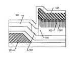
ここで、ドレイン領域(ドレイン電極114と接する半導体層)を拡大したものを図3に示す。図3において、103はゲイト電極、301はチャネル形成領域、302はn+層(ソースまたはドレイン電極)、303、304は膜厚の異なるオフセット領域、305はn-層(LDD領域)である。
【0066】
なお、ここでは説明しないがソース領域(ソース電極113と接する半導体層)も同様の構造を有している。
【0067】
また、図3に示す構造は模式的に記されているが、各領域の膜厚関係には注意が必要である。本願発明を構成するにあたって最も好ましい構成は、膜厚の厚さがn+層302<n-層305<オフセット領域(i層)304の関係にある場合である。
【0068】
なぜならばn+層302は電極として機能するだけなので薄くで十分である。一方、n-層305及びオフセット領域304は電界緩和を効果的に行うために適切な厚さが必要である。
【0069】
本実施例の構成では、チャネル形成領域301からn+領域302に至るまでに膜厚の異なる二つのオフセット領域303、304及びLDD領域305が存在する。なお、303はマスク合わせにより形成される膜面方向のオフセット領域であり、マスクオフセット領域と呼ぶ。
【0070】
また、304はi層の膜厚分に相当する膜厚方向のオフセット領域であり、厚さオフセット領域と呼ぶ。厚さオフセット領域304の厚さは100 〜300 nm(代表的には 150〜200nm )の範囲で決定すれば良い。ただし、チャネル形成領域の膜厚よりも膜厚をが厚くする必要がある。チャネル形成領域よりも膜厚が薄いと良好なオフセット効果を望めない。
【0071】
この様なオフセット+LDDからなる構造を本発明者らはHRD(High Resistance Drain )構造と呼び、通常のLDD構造とは区別して考えている。本実施例の場合、HRD構造はマスクオフセット+厚さオフセット+LDDの3段構造で構成されることになる。
【0072】
この時、LDD領域303はLDD領域の膜厚及び不純物濃度によって制御されるため、非常に再現性が高く、特性バラツキが小さいという利点を有する。パターニングによって形成されたLDD領域ではパターニング誤差による特性バラツキが問題となることは従来例で述べた通りである。
【0073】
なお、マスクオフセット領域303の長さ(X1 )はパターニングによって制御されるため、パターニングやガラスの縮み等による誤差の影響を受ける。しかしながら、その後に厚さオフセット領域304とLDD領域305とが存在するので誤差による影響は緩和され、特性バラツキを小さくすることができる。
【0074】
なお、マスクオフセットの長さ(X1 )はチャネル長(L1 )とチャネルエッチ領域の長さ(C1 )を用いて(C1 −L1 )/2で表される。従って、ソース/ドレイン電極形成時のパターニング工程によって所望のオフセット長(X1 )を設定することが可能である。本実施例の構成ではオフセット長(X1 )は 0.3〜3μm(代表的には1〜2μm)とすることができる。
【0075】
なお、図2(D)に示す様な構造の逆スタガ型TFTは、従来の非晶質珪素膜を活性層(島状半導体層)として利用したTFTでは実現できない。なぜならば、非晶質珪素膜を用いる場合、ソース/ドレイン電極とゲイト電極とがオーバーラップする様な構造にしないとキャリア(電子または正孔)の移動度が極めて遅くなってしまうからである。
【0076】
ソース/ドレイン電極とゲイト電極とがオーバーラップする様な構造にしたとしても非晶質珪素膜を用いたTFTのモビリティ(電界効果移動度)はせいぜい1〜10cm2 /Vs程度である。それに対して本実施例の様な構造を採用してしまってはモビリティが低すぎてスイッチング素子として機能しない。
【0077】
ところが、本願発明では活性層として結晶性珪素膜を利用しているのでキャリア移動度が十分に速い。従って、本実施例の様な構造としても十分なモビリティを得ることが可能である。即ち、本実施例の構造は半導体層として結晶構造を有する半導体膜を用いたからこそ実現できるのである。
【0078】
また、本実施例の逆スタガ型TFTは、HRD構造を有しているので衝突電離によるホットキャリア注入などの劣化現象に対して非常に強く、高い信頼性を有している。しかも、LDD領域の効果が支配的な上、そのLDD領域が非常に制御性よく形成されているので特性バラツキが非常に小さい。
【0079】
そのため、本実施例の様な構造は高耐圧を必要とし、高い動作速度はそれほど必要としない様な回路を構成するTFTに好適である。
【0080】
また、本実施例の作製工程に示した様に、図2(D)に示した構造の逆スタガ型TFTを得るのに4枚のマスクしか必要としていない。これは従来のチャネルストップ型TFTが6枚マスクを必要としていた事を考えると、スループット及び歩留りが飛躍的に向上することを意味している。
【0081】
以上の様に、本実施例の構成によれば量産性の高い作製工程によって、高い信頼性と再現性を有するボトムゲイト型TFTを作製することが可能である。
【0082】
なお、本実施例の作製工程に従って作製したボトムゲイト型TFT(Nチャネル型TFT)のモビリティは30〜250cm2 /Vs (代表的には10〜150cm2 /Vs )、しきい値電圧は0〜3Vを実現しうる。
【0083】
〔実施例2〕
本実施例では本願発明の構成において、実施例1とは異なる構成例を示す。TFTの作製工程は基本的には実施例1に従えば良いので、本実施例では必要な部分のみを説明することにする。
【0084】
まず、実施例1の作製工程に従って図5(A)の状態を得る。ここで実施例1と異なる点は、ソース電極501、ドレイン電極502を形成する際にチャネルエッチ領域500の長さをC2 とする点にある。この時、C2 はゲイト電極幅よりも狭く、2〜9μm(代表的には2〜4μm)の範囲で選ばれる。即ち、ゲイト電極とソース/ドレイン電極とがオーバーラップする様に設けることが本実施例の特徴となる。
【0085】
この状態で実施例1に示した様にチャネルエッチ工程を行い、保護膜を設けると図5(B)の状態を得る。この時、503で示される領域がチャネル形成領域となり、そのチャネル長はL2 (=C2 )で表される。また、マスク設計によりオーバーラップさせた領域(マスクオーバーラップ領域と呼ぶ)504の長さ(Y2)はゲイト電極幅をEとすると、(E−L2 )/2で表される。
【0086】
図5(C)はドレイン領域の拡大図であるが、TFT動作時のキャリアは、チャネル形成領域503(厚さ50nm)、マスクオーバーラップ領域504(厚さ160 nm)、LDD領域505(厚さ50nm)を通ってn+層506(厚さ40nm)、ドレイン電極502へと到達する。
【0087】
なお、この場合、マスクオーバーラップ領域504にもゲイト電極からの電界が形成されるが、LDD領域505に近づくにつれて電界は弱まるので、その様な領域は実質的にLDD領域と同様の機能を持つ。勿論、さらにLDD領域505に近づけば完全に電界が形成されなくなり、オフセット(厚さオフセット)領域としても機能しうる。
【0088】
この様に本実施例の構造ではHRD構造が、オーバーラップによる実質的なLDD+厚さオフセット+低濃度不純物によるLDDで構成される。また、オーバーラップ領域504の膜厚が薄い場合には、オーバーラップによる実質的なLDD+低濃度不純物によるLDDのみからなるLDD構造もとりうる。
【0089】
本実施例の構成においても、オーバーラップ領域504、LDD領域505がそれぞれの膜厚で制御されるので非常に特性バラツキが小さい。また、オーバーラップ領域の長さ(Y2 )はパターニング等による誤差を含むが、オーバーラップによるLDD、厚さ方向のオフセット及び低濃度不純物によるLDDはその様な誤差の影響を受けないのでY2 の誤差による特性バラツキは緩和される。
【0090】
なお、本実施例の様な構造はオフセット成分が少なく、高い動作速度を必要とする様な回路を構成するTFTに好適である。
【0091】
また、本実施例の構造では衝突電離によってチャネル形成領域内に蓄積した少数キャリアが速やかにソース電極へと引き抜かれるので基板浮遊効果を起こしにくいという利点を有する。そのため、動作速度が速い上に非常に耐圧特性の高いTFTを実現することが可能である。
【0092】
〔実施例3〕 本実施例では本願発明の構成において、実施例1、2とは異なる構成例を示す。TFTの作製工程は基本的には実施例1に従えば良いので、本実施例では必要な部分のみを説明することにする。
【0093】
まず、実施例1の作製工程に従って図6(A)の状態を得る。ここで実施例1と異なる点は、ソース電極601、ドレイン電極602を形成する際にチャネルエッチ領域600の長さをC3 とする点にある。この時、C3 はゲイト電極幅と一致させるため、1〜10μm(代表的には3〜5μm)となる。
【0094】
この状態で実施例1に示した様にチャネルエッチ工程を行い、保護膜を設けると図6(B)の状態を得る。この時、603で示される領域がチャネル形成領域となり、そのチャネル長はL3 (=C3 )で表される。
【0095】
図6(C)はドレイン領域の拡大図であるが、TFT動作時のキャリアは、チャネル形成領域603(厚さ100 nm)、厚さオフセット領域604(厚さ150 nm)、LDD領域605(厚さ100 nm)を通ってn+層606(厚さ50nm)、ドレイン電極602へと到達する。即ち、本実施例の構造ではHRD構造が厚さオフセット+LDDの2段構造で構成される。
【0096】
本実施例の構成においても、厚さオフセット領域604、LDD領域605がそれぞれの膜厚で制御されるので非常に特性バラツキが小さい。また、十分な耐圧特性を得ることが可能である。
【0097】
〔実施例4〕 本実施例では本願発明の構成において、実施例1〜3とは異なる構成例を示す。TFTの作製工程は基本的には実施例1に従えば良いので、本実施例では必要な部分のみを説明することにする。
【0098】
まず、実施例1の作製工程に従って図7(A)の状態を得る。ここで実施例1と異なる点は、ソース電極701、ドレイン電極702を形成する際にソース電極またはドレイン電極のいずれか一方をゲイト電極にオーバーラップさせ、他方はオーバーラップさせない構成とする点にある。
【0099】
なお、本実施例ではチャネルエッチ領域700の長さをC4 とする。この時、C4 は1〜10μm(代表的には3〜6μm)の範囲で選ばれる。
【0100】
この状態で実施例1に示した様にチャネルエッチ工程を行い、保護膜を設けると図7(B)の状態を得る。この時、703で示される領域がチャネル形成領域となり、そのチャネル長はL4 (=C4 −X4 )で表される。
【0101】
ここで、X4はマスクオフセット領域704の長さである。X4 の数値範囲については実施例1を参考にすれば良い。また、マスクオーバーラップ領域705の長さの数値範囲は実施例2を参考にすれば良い。
【0102】
本実施例は、実施例1で説明したHRD構造と実施例2で説明したHRD構造(またはLDD構造)とを組み合わせた構成である。構造的な説明は実施例1及び実施例2で既に説明したのでここでの説明は省略する。
【0103】
本実施例の様な構造を採用する場合、特にソース領域に実施例2に示したHRD構造(またはLDD構造)を用い、ドレイン領域に実施例1で説明したHRD構造を用いることが好ましい。
【0104】
例えば、ドレイン領域側のチャネル端部(接合部)では特に電界集中が激しく、実施例1に示した様な抵抗成分の多いHRD構造が望ましい。逆に、ソース側ではそこまでの高耐圧対策は必要ないので、実施例2に示した様な抵抗成分の少ないHRD(またはLDD)構造が適している。
【0105】
なお、本実施例において、ソース/ドレイン領域側のいずれか一方に実施例2の構成を組み合わせることも可能である。この様に、実施例1〜3に示したHRD構造またはLDD構造を実施者が適宜選択してソース/ドレイン領域に採用し、回路設計を鑑みて最適な構造を設計すれば良い。この場合、32 =9通りの組み合わせパターンが可能である。
【0106】
〔実施例5〕 本実施例では実施例1〜4に示した構成のボトムゲイト型TFTを用いてCMOS回路(インバータ回路)を構成する場合の例について図8を用いて説明する。なお、CMOS回路は同一基板上に形成されたNチャネル型TFTとPチャネル型TFTとを相補的に組み合わせて構成する。
【0107】
図8は実施例4に示した構成を利用したCMOS回路であり、801はPチャネル型TFTのソース電極、802はNチャネル型TFTのソース電極、803はN/P共通のドレイン電極である。
【0108】
また、Nチャネル型TFTは実施例1で説明した作製工程によってn+層804、805、n-層806、807が形成されている。一方、Pチャネル型TFTの方にはp++層808、809、p-層810、811が形成されている。
【0109】
なお、同一基板上にCMOS回路を作製することは非常に容易である。本願発明の場合、まず、実施例1の工程に従って図2(B)の状態を得る。
【0110】
この状態ではN型/P型関係なく15族から選ばれた元素が全面に添加されているが、Pチャネル型TFTを作製する場合にはNチャネル型TFTとする領域をレジストマスク等で隠して13族から選ばれた元素(代表的にはボロン、インジウムまたはガリウム)を添加すれば良い。
【0111】
本実施例ではボロンを例にとるが、この時、ボロンはリンの濃度以上に添加して導電性を反転させなければならない。また、n+層及びn-層全てを完全にp++層及びp-層に反転させるためには、ボロン添加時の濃度プロファイルを調節してリンの添加深さよりも深く添加することが重要である。
【0112】
従って、ボロンの膜中における濃度プロファイルは図9の様になる。図9において、900は半導体層、901はボロン添加前のリンの濃度プロファイル、902はボロン添加後のボロンの濃度プロファイル、903はp++層、904はp-層、905はi層である。
【0113】
この時、p++層903の厚さは10〜150 nm(代表的には50〜100 nm)とし、p++層のボロンの濃度は、3×10¹⁹〜1×10²²atoms/cm3 、代表的には3×10¹⁹〜3×10²¹atoms/cm3 となる様に調節する。
【0114】
他方、p-層904の厚さは30〜300 nm(代表的には 100〜200 nm)とし、そのボロンの濃度は、5×10¹⁷〜3×10¹⁹atoms/cm3 となる様に調節する。する。ただし、Pチャネル型TFTは元来劣化に強いのでp-層をLDD領域として利用する必要性は必ずしもない。わざわざp-層904の膜厚について言及したのは、イオン注入法等の添加手段を用いる限り、連続的に変化する濃度勾配によって必ずp-層が形成されるからである。
【0115】
ところで、本実施例ではNチャネル型TFTとPチャネル型TFTのどちらもソース領域側には実施例2に示した構成のHRD構造(オーバーラップ領域を利用したタイプ)を用い、ドレイン領域側には実施例1に示した構成のHRD構造(マスクオフセットを利用したタイプ)を設けている。
【0116】
そのため、上面図で明らかな様にPチャネル型TFTのソース領域側にはYiの長さを持つオーバーラップ領域を有し、ドレイン領域側にはXiの長さを持つマスクオフセット領域を有している。また、Nチャネル型TFTのソース領域側にはYjの長さを持つオーバーラップ領域を有し、ドレイン領域側にはXjの長さを持つマスクオフセット領域を有している。
【0117】
この時、XiとXj、YiとYjの長さはそれぞれマスク設計によって自由に調節できる。従って、それぞれの長さは回路構成の必要に応じて適宜決定すれば良く、Nチャネル型とPチャネル型とで揃える必要はない。
【0118】
また、この様な構造ではCMOS回路の共通ドレインとなる領域の耐圧特性を高くすることができるので、動作電圧の高い回路を構成する場合において、非常に有効な構成である。
【0119】
なお、実施例1〜4に示した構成のTFTを用いたCMOS回路の構成を図8に示したが、これ以外の全ての組み合わせも可能であることは言うまでもない。可能な構成パターンとしては、一つのTFTについて9通りあるので、CMOS回路では92 =81通りがある。これらの複数の組み合わせの中から、回路が必要する性能に応じて最適な組み合わせを採用していけば良い。
【0120】
また、本実施例に示した様に本願発明はPチャネル型TFTにも容易に適用することができる。その場合、本願発明のボトムゲイト型TFT(Pチャネル型TFT)のモビリティは30〜150cm2/Vs (代表的には10〜100cm cm2/Vs )、し
きい値電圧は−1〜−3Vを実現しうる。
【0121】
〔実施例6〕 本実施例では、珪素の結晶化を助長する触媒元素としてGe(ゲルマニウム)を利用した場合の例をついて説明する。Geを利用する場合、汎用性の高さからイオン注入法、イオンドーピング法またはプラズマ処理による添加を行うことが好ましい。また、Geを含む雰囲気中で熱処理を行うことで気相から添加することも可能である。
【0122】
GeはSi(シリコン)と同じ14族に属する元素であるため、Siとの相性が非常に良い。GeとSiとの化合物(SixGe1-xで示される。ただし0<X<1)は本願発明の半導体層として活用することもできることは既に述べた。
【0123】
そのため、本実施例の様にGeを用いた非晶質珪素膜の結晶化を行った場合、結晶化後に触媒元素をゲッタリングする必要性がない。勿論、ゲッタリング工程を行っても構わないが、TFT特性に影響はない。
【0124】
従って、ゲッタリング工程の加熱処理を省略することができるので製造工程のスループットが大幅に向上する。また、SixGe1-x膜を用いたTFTは高いモビリティを示すことが知られているので、珪素膜中におけるGeの含有量が適切であれば動作速度の向上も期待しうる。
【0125】
なお、本実施例の構成は実施例1〜5のいずれの構成に対しても適用することが可能である。
【0126】
〔実施例7〕 本実施例では、本願発明のTFTに対してしきい値電圧を制御するための工夫を施した場合の例について説明する。
【0127】
しきい値電圧を制御するために13族(代表的にはボロン、インジウム、ガリウム)または15族(代表的にはリン、砒素、アンチモン)から選ばれた元素をチャネル形成領域に対して添加する技術はチャネルドープと呼ばれている。
【0128】
本願発明に対してチャネルドープを行うことは有効であり、以下に示す2通りの方法が簡易で良い。
【0129】
まず、非晶質珪素膜を成膜する時点において成膜ガスにしきい値電圧を制御するための不純物を含むガス(例えばジボラン、フォスフィン等)を混在させ、成膜と同時に所定量を含有させる方式がある。この場合、工程数を全く増やす必要がないが、N型及びP型の両TFTに対して同濃度が添加されるため、両者で濃度を異ならせるといった要求には対応できない。
【0130】
次に、図2(D)で説明した様なチャネルエッチ工程(チャネル形成領域の形成工程)が終了した後で、ソース/ドレイン電極をマスクとしてチャネル形成領域(またはチャネル形成領域とマスクオフセット領域)に対して選択的に不純物添加を行う方式がある。
【0131】
添加方法はイオン注入法、イオンドーピング法、プラズマ処理法、気相法(雰囲気からの拡散)、固相法(膜中からの拡散)など様々な方法を用いることができるが、チャネル形成領域が薄いので、気相法や固相法等の様にダメージをあたえない方法が好ましい。
【0132】
なお、イオン注入法等を用いる場合には、TFT全体を覆う保護膜を設けてから行えばチャネル形成領域のダメージを減らすことができる。
【0133】
また、不純物を添加した後はレーザーアニール、ランプアニール、ファーネスアニールまたはそれらを組み合わせて不純物の活性化工程を行う。この時、チャネル形成領域が受けたダメージも殆ど回復する。
【0134】
本実施例を実施する場合、チャネル形成領域には1×10¹⁵〜 5×10¹⁸atoms/cm3 (代表的には 1×10¹⁵〜 5×10¹⁷atoms/cm3 )の濃度でしきい値電圧を制御するための不純物を添加すれば良い。
【0135】
そして、本実施例を本願発明のTFTに実施した場合、Nチャネル型TFTのしきい値電圧を 0.5〜2.5 Vの範囲に収めることができる。また、Pチャネル型TFTに適用した場合にはしきい値電圧を-0.1〜-2.0Vの範囲に収めることが可能である。
【0136】
なお、本実施例の構成は実施例1〜6のいずれの構成との組み合わせも可能である。また、実施例5のCMOS回路に適用する場合、N型TFTとP型TFTとで添加濃度や添加する不純物の種類を異なるものとすることもできる。
【0137】
〔実施例8〕 図2(D)に示した構造では、島状半導体層を完全に囲む様にしてソース電極113とドレイン電極114とが形成されている。本実施例ではこれとは別の構成について説明する。
【0138】
図10(A)に示す構造は、基本的には図2(D)と似ているが、ソース電極11及びドレイン電極12の形状が異なる点に特徴がある。即ち、一部において島状半導体層(厳密にはソース/ドレイン領域)よりもaで示される距離だけ内側にソース電極11及びドレイン電極12が形成されている。
【0139】
また、13で示される領域は、チャネル形成領域14と同じ膜厚を有する領域であり、距離aの幅を持つ。図面上では模式的に表しているが、距離aは1〜300 μm(代表的には10〜200 μm)である。
【0140】
ここで作製工程と照らし合わせて本実施例の特徴を説明する。本実施例では図10(B)に示す様にソース電極11及びドレイン電極12を形成する。ここで15は島状半導体層であり、端部16が露出する。
【0141】
この状態でチャネルエッチ工程を行うと、ソース電極11及びドレイン電極12がマスクとなって自己整合的に島状半導体層15がエッチングされる。この場合、端部16も同時にエッチングされる。
【0142】
この様にして図10(A)の様な構造が得られる。従って、端部16がチャネル形成領域14と同じ膜厚を有することは明らかである。
【0143】
この島状半導体層の突出部13を形成する理由は以下の2つがある。
(1)チャネルエッチ工程におけるエッチングモニタとして利用する。
(2)後工程で保護膜や層間絶縁膜を形成する際に、島状半導体層の段差によるカバレッジ不良を低減する。
【0144】
エッチングモニタとしては、製造過程における抜き取り検査によってチャネル形成領域が適切な膜厚となっているかどうかを検査する場合に用いる。
【0145】
なお、本実施例の構成は実施例1〜7のいずれの構成とも組み合わせることが可能である。
【0146】
〔実施例9〕 本実施例では実施例5に示したCMOS回路(インバータ回路)の回路構成の例について図11を用いて説明する。
【0147】
図11(A)に示すのは、図8に示したものと同一構造のCMOS回路である。この場合、回路構成はゲイト電極20、N型TFTの半導体層21、P型TFTの半導体層22、N型TFTのソース電極23、P型TFTのソース電極24、共通ドレイン電極25から構成される。
【0148】
なお、各端子部a、b、c、dはそれぞれ図11(C)に示したインバータ回路の端子部a、b、c、dに対応している。
【0149】
次に、図11(B)に示すのは、N型TFTとP型TFTとでドレイン領域となる半導体層を共通化した場合の例である。各符号は図11(A)で説明した符号に対応している。
【0150】
図11(B)の構造ではTFT同士を非常に高い密度で形成することができるため、回路を高集積化する場合などに非常に有効である。共通化した半導体層はPN接合を形成するが問題とはならない。
【0151】
〔実施例10〕 本実施例では、実施例1〜5の構成のTFT及びCMOS回路を作製する過程において、加熱処理の手段としてランプアニールを用いる場合の例を示す。
【0152】
ランプアニールとしてはRTA(Rapid Thermal Anneal)による熱処理が知られている。これは赤外ランプからの強光を照射することにより短時間(数秒から数十秒)で高温の加熱処理を行う技術であり、スループットが非常に良い。また、赤外光以外に補助的に紫外光を用いる場合もある。
【0153】
本願発明においては、非晶質半導体膜の結晶化工程、結晶性半導体膜の結晶性改善工程、触媒元素のゲッタリング工程、しきい値制御のための不純物の活性化工程等に加熱処理を行う。この様な時に本実施例を利用することができる。
【0154】
なお、本実施例の構成と他の実施例の構成とは自由に組み合わせることが可能である。
【0155】
〔実施例11〕 本実施例では実施例1とは異なる手段で触媒元素のゲッタリングを行う場合について説明する。
【0156】
実施例1では15族から選ばれた元素のみを利用してゲッタリング工程を行っているが、触媒元素のゲッタリング工程は13族及び15族から選ばれた元素が添加された状態でも実施することができる。
【0157】
その場合、まず図1(E)に示す状態を得たら、Nチャネル型TFTとなる領域のみをレジストマスクで隠して次にボロンを添加する。即ち、Nチャネル型TFTとなる領域にはリンのみが存在し、Pチャネル型TFTとなる領域にはボロンのみが存在する。
【0158】
そして、その状態で加熱処理を行い、触媒元素のゲッタリング工程を実施すれば良い。本発明者らの実験ではリンのみによるゲッタリング効果よりもリン+ボロンによるゲッタリング効果の方が効果が高いことが確かめられている。ただし、ボロンのみではゲッタリング効果はなく、リン+リンよりも高濃度のボロンという組み合わせの時に高いゲッタリング効果を示した。
【0159】
なお、本実施例の構成と他の実施例の構成とは自由に組み合わせることが可能である。
【0160】
〔実施例12〕 基板として耐熱性の高い石英基板やシリコン基板を用いている場合、n+導電層及びn-導電層を形成する前にハロゲン元素を含む酸化性雰囲気中で700 〜1100℃程度の加熱処理を行うことも有効である。これはハロゲン元素による金属元素のゲッタリング効果を利用する技術である。
【0161】
また、この技術と実施例11に示した様なゲッタリング工程とを併用することでさらに徹底的に非晶質半導体膜の結晶化に利用した触媒元素を除去することができる。こうして、触媒元素を少なくともチャネル形成領域から徹底的に除去しておけば信頼性の高い半導体装置を得ることができる。
【0162】
〔実施例13〕 本実施例は、実施例1〜4で説明したTFTを画素マトリクス回路の画素TFTに適用したものであり、ここでは、TFTを実施例4で示したオフセット構造とオーバーラップ構造を複合した構造とする。
【0163】
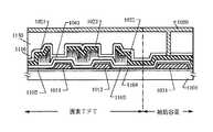
図12は、本実施例の画素マトリクス回路の1画素の模式的な平面図であり、図13は断面図である。画素マトリクス回路の各画素には、画素TFTと補助容量が形成されている。画素マトリクス回路には、画素TFTのオン/オフを制御する信号を入力するための複数のゲイト配線1010がX方向に平行に配列され、画像信号を入力するための複数のソース配線1020がY方向に平行に配列されている。
【0164】
画素マトリクス回路の作製工程は実施例1と同様の工程条件にて作製されるため、本実施例の作製工程の説明は簡略化する。ガラス基板1101表面には、酸化珪素膜でなる下地膜1102が形成されている。下地膜1102上には、1層目の配線として、ゲイト配線1010及びゲイト配線1010と平行に容量配線30とが形成されている。1層目の配線を構成する導電膜として、下層にTaN膜、上層にTa膜でなる積層膜を用いる。ゲイト配線1010には、TFTのゲイト電極1011、1012が一体的に形成され、容量配線1030には補助容量の下部電極となる容量電極1031が一体的に形成されている。
【0165】
第1層目の配線・電極上には、窒化珪素膜1103および窒化酸化珪素膜1104でなるゲイト絶縁層が形成される。絶縁層1103、1104上には、画素TFTの半導体層1041が形成される。本実施例では、画素TFTはゲイト電極1011を有するTFTと、ゲイト電極1012を有するTFTとが直列に接続された構成となる、いわゆるマルチゲイト型とすることによりリーク電流の低減を図る。
【0166】
2層目の配線として、Ti/Al/Tiの積層膜でなるソース配線1020、ソース電極1021、ドレイン電極1022、マスク電極1023が形成されている。ソース電極1021はデータ配線1020と一体的に形成されている。ソース配線1020は、ゲイト配線1010及び容量配線1030に対して格子を成すように配置され、これら配線1010、1030とはゲイト絶縁層のみによって絶縁されている。
【0167】
このため、1層目の配線1010、1030と、2層目の配線1020間の寄生容量を小さくするため、ゲイト絶縁層の厚さをトップゲイト型TFTと比較して厚めにする。ここでは厚さを0.3〜0.8μm、代表的には0.4〜0.5μmとする。よって、ゲイト絶縁層と構成する1層目の窒化珪素膜1103の厚さを0〜500nm、代表的には25〜300nmする。2層目の窒化酸化珪素膜(もしくは酸化珪素膜)1104の厚さを0〜800nm、代表的には150〜500nmとする。ここでは、窒化珪素膜1103の厚さを150nmとし、窒化酸化珪素膜1104の厚さを300nmとする。
【0168】
2層目の電極1021、1022、1023をマスクにして、画素TFTの半導体層1041はチャネルエッチングが施されている。マスク電極1023の電位はフローティングとされ、半導体層1041に電圧を印加する機能はなく、チャネルエッチ工程時にマスクとして機能するものである。ここでは、ソース電極1021、ドレイン電極1022をゲイト電極1011、1021に対してオフセットし、他方、マスク電極23はゲイト電極1011、1021に対してオーバーラップするように形成する。
【0169】
この構造において、ソース領域、およびドレイン領域には、実施例1で説明したオフセット型のHRDが形成され、高耐圧対策が施されている。他方、マスク電極1023の下層の不純物領域は2つのTFTの連結部に相当し、キャリアの経路としてのみ機能するため、高移動度が最優先される。従って、この不純物領域には実施例2で説明したオーバーラップ型のHRD領域を設け、移動度の向上を図る。
【0170】
なお、画素マトリクス回路では画素電極に極性が交互に反転するように電圧を印加するため、正負双方の極性の電圧に対しても画素TFTの特性が等しくなるようにするのが好ましい。本実施例では、ソース領域とドレイン領域に形成されるオフセット領域の長さが等しくなるように、またマスク電極1023の両側に形成されるオーバーラップ領域の長さが等しくなるように設計する。
【0171】
実施例1、2で示したように、オフセット長及びオーバーラップ長は1層目、2層目の配線のパターンによって決定され、それぞれ0.3〜3μmをとることができる。ここではオフセット長、オーバーラップ長をそれぞれ1μmとする。また画素TFTの場合には、チャネル幅及びチャネル長が1〜10μmとなるようにする。ここでは、チャネル幅を5μmとし、チャネル長を3μmとする。チャネル長を3μmとするため、ゲイト電極1011、1012幅は3μmとする。なお、マスク電極1023の両側のオーバーラップ長は実施例3に示すように、ゼロとなるようにしてもよい。
【0172】
マスク電極1023はゲイト電極1011、1021に対してオーバーラップされて配置されているので、マスク電極1023とゲイト電極1011、1012間の寄生容量を小さくするため、マスク電極1023は半導体層1041の幅よりも狭くする。
【0173】
他方、補助容量において、ドレイン電極1022は容量電極1031と対向するように形成されている。この構造により、ドレイン電極1022と容量電極1031を対向電極とし、ゲイト絶縁層1103、1104を誘電体とする補助容量が形成される。実施例1で示したように、画素TFTは4枚のマスクで形成でき、また、補助容量1030を追加してもマスクパターンの変更のみであり、マスク数は増加しないことは明らかである。これは従来のチャネルストップ型TFTだけを作製するのに、6枚マスクを必要としていた事を考えると、スループット及び歩留りが飛躍的に向上することを意味している。
【0174】
画素TFT、補助容量を覆って、厚さ100〜250nmの窒化酸化珪素または窒化珪素でなる保護膜1116が形成される。ここでは、厚さ200nmの窒化酸化珪素膜を形成する。
【0175】
保護膜1116上に、画素電極1050の下地となる厚さ0.8〜1.5μmの層間絶縁膜1130が形成される。層間絶縁膜1130としては、平坦な表面を得られる塗布膜が好ましい。塗布膜の1つとして、ポリイミド、ポリアミド、ポリイミドアミド、アクリル等の樹脂膜や、PSGや酸化珪素等の酸化珪素系の塗布膜が使用できる。本実施例では、層間絶縁膜1130としてアクリル樹脂膜を1.0μmの厚さに形成する。
【0176】
そして、層間絶縁膜1130および保護膜1117にドレイン電極1022に達するコンタクトホールを形成する。ここでマスク数は5となる。次に透明導電膜として厚さ100〜150nmのITO膜を形成する。ここでは、120nmの厚さに成膜し、パターニングして画素電極1050を形成する。これでマスク数が6になる。以上の工程により、画素マトリクス回路が完成する。なお、画素電極1050の材料をAl等の金属膜として、反射電極を作製しても良い。
【0177】
補助容量の誘電体を窒化珪素膜1103と窒化酸化珪素膜(酸化珪素膜)1104の2層の絶縁体としたが、下層の窒化珪素膜1103のみを用いることも可能である。この場合には、図2(B)に示す島状半導体層のパターニング後に、半導体層をマスクにして露出されている窒化酸化珪素膜1104をエッチングにより除去し、この後2層目の配線となるソース配線1020、電極1021、1022、1023を形成する。ただし窒化酸化珪素膜1104をエッチングするには、窒化珪素膜1103がエッチングストッパーとして機能するようなエッチングガスもしくはエッチャントを用いる必要がある。また、窒化酸化珪素膜1104がよりエッチングしやすくなるように、その組成を調整したり、窒化酸化珪素膜の代わりに酸化珪素膜を成膜するのも有効である。
【0178】
実施例5及び9で説明したように、nチャネル型の画素TFTとCMOSTFTでなるインバータ回路を同時に形成することが可能である。この技術を用いて、図示していないが画素マトリクス回路を駆動する周辺駆動回路も同一基板1101上に形成されている。周辺駆動回路に配置されるTFTは高速動作を優先させるため、ソース/ドレイン領域はオーバーラップ構造とするのがよい。
【0179】
本実施例の画素TFTは2つのゲイト電極を有するマルチゲイト型としたが、ゲイト電極数は2に限定されるものではなく、1もしくは2以上とすることができる。何れのゲイト電極数でも、ソース配線1020及び画素電極1050によって電圧が印加されるソース及びドレイン領域はオフセット構造とし高耐圧対策を施すと良い。またゲイト数が2以上の場合にはソース及びドレイン領域以外の不純物領域が半導体層に形成されるが、この不純物領域はゲイト電極に対して、オーバーラップさせるか、もしくは実施例3で示したようにオフセット長及びオーバーラップ長がゼロとなるように形成して、高移動度を優先すると良い。
【0180】
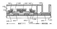
〔実施例14〕 本実施例では実施例13の補助容量の変形例を示す。図14に本実施例の画素マトリクス回路の断面図を示す。なお図14おいて、図12、13と同じ符号は実施例13と同じ構成要素であり、実施例13と異なるのは、画素TFTの半導体層1241及びドレイン電極1222のパターンである。
【0181】
本実施例では、図2(B)に示す島状半導体層をパターニング工程によって、半導体層を容量電極31と対向するように形成する。そして、ドレイン電極1222を容量電極1031に部分的にオーバーラップするように形成する。島状半導体層を電極1021、1023、1222をマスクにしてチャネルエッチングを施す。この結果、半導体層1241はチャネルエッチングにより、容量電極1031上には真性又は実質的に真性なi層でなるi型領域1242が形成される。このi型領域1242は画素TFTのチャネル形成領域とほぼ同じ膜厚であり、同様な機能を有する
【0182】
容量電極1031により電圧を印加すると、i型領域1242にはチャネルが形成される。更にドレイン電極1222と容量電極1031がオーバーラップしている半導体層1241のi層、即ち図5のマスクオーバーラップ領域にもチャネルが形成される。これらチャネルが補助容量の上部電極として機能する。補助容量の上部電極と画素電極1050の接続構造は、図5に図示されたチャネル形成領域とドレイン電極との接続構造と同じである。図5を参照すると、i層でなるi型領域1242(503)、マスクオーバーラップ領域(504)、n-層でなるLDD領域(505)、n+層(506)、ドレイン電極1222(502)、画素電極1050の順になる。
【0183】
ここでは、補助容量の上部電極の主要な部分がi型領域1242になるように、マスクオーバーラップ領域長を設定するのが好ましく、0.3〜3μm程度とする。またドレイン電極1222と容量電極1031をオーバーラップ構造としたのは、画素電極1050間と上記の補助容量の上部電極間の抵抗が小さくなるようにするためである。なお、i型領域1224により低い電圧でチャネルを形成するには、実施例7で示したしきい値制御対策を施すことが好ましい。
【0184】
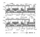
〔実施例15〕 図15に本実施例の画素マトリクス回路の断面図を示す。本実施例では実施例14と同様に画素TFTの半導体層のi層を補助容量の上部電極に用いる例を示す。なお、図15において、図14と同じ符号は実施例14と同じ構成要素である。実施例14と異なるのは、画素TFTの半導体層1341及びドレイン電極1322のパターンである。
【0185】
実施例14では容量電極1031と対向する半導体層1241にチャネルエッチングが施されているが、本実施例では容量電極と対向する半導体層1341にチャネルエッチングを施さないようにする。そのためドレイン電極1322は容量電極1031と対向する半導体層1342の表面を覆うように形成される。
【0186】
この構造において、補助容量の上部電極は、容量電極1031の電圧によって半導体層1342のi層に形成されるチャネルとなる。このチャネルが形成される領域は、実施例2で説明したオーバーラップ領域504(図5参照)に対応する。従って、補助容量の上部電極と画素電極1050接続構造は、図5を参照すると、i層でなるマスクオーバーラップ領域(504)、n-層でなるLDD領域(505)、n+層(506)、ドレイン電極1322(502)、画素電極1050の順になる。
【0187】
補助容量と上部電極となる半導体層1341のi層(マスクオーバーラップ領域)により低い電圧でチャネルを形成するには、実施例7で示したしきい値制御を対策を施すことが好ましい。
【0188】
〔実施例16〕 図16に本実施例の画素マトリクス回路の断面図を示す。本実施例は実施例15の変形例である。図16おいて、図15と同じ符号は実施例15と同じ構成要素であり、実施例15と異なるのは、画素TFTにおいては、半導体層1441及びドレイン電極1422のパターンと、画素電極1450の接続構造であり、更に補助容量においては、画素TFTと分離して、半導体層1442と第2層目の電極1424が形成されている点である。
【0189】
本実施例では、図2(B)に示す島状半導体層のパターニング工程において、画素TFTの半導体層1441の原型となる島状領域と、補助容量の半導体層1442を形成する。つぎに2層目の配線ソース電極1022、マスク電極1023、ドレイン電極1422及び電極1424を形成する。電極1424は補助容量の半導体層1424がチャネルエッチングされないように、半導体層1424を被覆している。チャネルエッチングを行うことにより、画素TFTの半導体層1441が形成される。
【0190】
次に保護膜1116、層間絶縁膜1130を形成する。保護膜1116、層間絶縁膜1130にドレイン電極1422、補助容量の電極1424に達するコンタクトホールを形成した後、画素電極1450を形成する。図16(A)に示すように画素電極1450はドレイン電極1422及び電極1422と電気的に接続される。
【0191】
補助容量の構造は実施例15と実質的に同様であり、補助容量の上部電極は、半導体層1442のi層に形成されるチャネルである。このi層は図5のマスクオーバーラップ領域に対応する。補助容量の上部電極と画素電極1450の接続構造は、半導体層1442のi層でなるマスクオーバーラップ領域(504)、n-層でなるLDD領域(505)、n+層(506)、電極1424(502
)、画素電極1450の順になる。
【0192】
なお、本実施例ではn+層が電極として機能できる。よって図16(B)に示すように、画素電極1450用のコンタクトホールを形成する工程において、電極1424にもエッチングして、半導体層1424のn+層を接続する。
【0193】
また、図16(A)、(B)において半導体層1442にはチャネルエッチングを施さないようにしたが、画素電極1450との接続部を少なくとも覆うようにして、実施例8に示すように半導体層1442の側面に突出部を形成し、半導体層1442の段差を緩和しても良い。
【0194】
〔実施例17〕 図17に本実施例の画素マトリクス回路の断面図を示す。本実施例は実施例16の変形例である。図17おいて図16と同じ符号は実施例16と同じ構成要素であり、実施例16と異なるのは、実施例16の補助容量の半導体層1442と電極1424を形成しない点と、画素電極1550の接続構造である。
【0195】
本実施例では画素電極1550を補助容量の上部電極とする。画素電極1550用のコンタクトホールを形成する工程において、層間絶縁膜1130、窒化酸化珪素膜でなる保護膜1116及びゲイト絶縁層の第2層1104がエッチングされるため、補助容量の誘電体はゲイト絶縁膜の第1層の窒化珪素膜1103となる。
【0196】
なお、本実施例では補助容量の誘電体に、窒化珪素膜1103、窒化酸化珪素膜(酸化珪素膜)1104、保護膜1116が使用できる。
【0197】
例えば、画素電極1550用のコンタクトホールを形成する際に、層間絶縁膜1130と保護膜1116のマスクパターンと変えて、補助容量のコンタクトホールの保護膜1116を除去しないようにすることで、列記した3つの膜を補助容量の誘電体に使用できる。
【0198】
例えば、保護膜1116を窒化珪素膜として、コンタクトホール形成工程では、ゲイト絶縁層の2層目の酸化窒化珪素膜(酸化珪素膜)1104がエッチングストッパーとなるような、エッチングガスもしくはエッチャントを使用すれば、が酸化窒化珪素膜(酸化珪素膜)11140及び窒化珪素膜1103を補助容量の誘電体とすることができる。
【0199】
〔実施例18〕 本実施例は実施例17の変形例である。実施例17では、補助容量の電極としてゲイト配線1010と別途に容量配線1030が必要であったが、本実施例では容量配線を省略する例を示す。図20に本実施例の画素マトリクス回路の平面図を示し、図18に模式的な断面図を示す。図20、図18において図17と同じ符号は同じ構成要素を示す。
【0200】
図20に示すように、本実施例のゲイト配線1210には画素TFTのゲイト電極1211、1212、及び補助容量の電極1231が一体的に形成されている。補助容量の電極として容量電極1231と画素電極1231を用いる点は実施例17と同様であるが、画素電極1231は次段もしくは前段のゲイト配線1230に形成された容量電極1231と対向している。
【0201】
図18は画素電極1650Bを有する画素の断面図に対応する。図20に示すように、画素電極1650Bは前段(次段)のゲイト配線1210Aに形成された容量電極1231Aと対向して、ゲイト絶縁層1103、1104を誘電体とする補助容量が形成される。またゲイト配線1210Bに形成された容量電極1231Bには次段(前段)の画素電極1650と対向している。
【0202】
また、本実施例の容量電極1231は、画素電極がドレイン電極と補助容量とでは異なる接続部を有する場合に適用することができ、実施例16にも適用可能である。図19(A)、(B)は、本実施例を実施例16(図16)に適用した場合の、画素マトリクス回路の断面図を示す。なお、図19の符号は図18を準用する。
【0203】
〔実施例19〕 第1層目の配線である容量配線・電極1030、1031の材料を陽極酸化可能な金属膜で形成することによって、容量電極1031の表面を陽極酸化して、陽極酸化膜を形成できる。この陽極酸化膜を補助容量の誘電体として用いることが可能である。
【0204】
実施例1で述べたリンゲッタリング工程に耐え、陽極酸化可能な金属膜として、Ta膜、MoTa合金膜等を用いることができる。本実施例の1層目の配線に用いたTaN/Taの積層膜も陽極酸化可能である。
【0205】
例えば本実施例を図17、18に示す画素マトリクス回路に応用した場合には、画素電極1550、1650用のコンタクトホールを形成する工程において、窒化珪素膜1103まで除去することにより、補助容量の誘電体を陽極酸化膜のみにすることができる。
【0206】
〔実施例20〕 図21を用いて、本実施例の表示装置を備えた電子機器を説明する。本実施例では、本発明による液晶表示装置を適用しうる応用製品(電気光学装置)について、実施例で示したAMLCDは様々な電子機器のディスプレイに利用される。なお、本実施例で挙げる電子機器とは、AMLCDを表示装置として搭載した製品を指す。
【0207】
本発明を応用した電気工学装置としてはビデオカメラ、スチルカメラ、プロジェクタ、ヘッドマウントディスプレイ、カーナビゲイション、パーソナルコンピュータ、携帯情報端末(モバイルコンピュータ、携帯電話)等が挙げられる。
【0208】
図21(A)はモバイルコンピュータ(モービルコンピュータ)であり、本体2001、カメラ部2002、受像部2003、操作スイッチ2004、表示装置2005で構成される。本発明は表示装置2005に適用される。
【0209】
図21(B)はヘッドマウントディスプレイであり、本体2201、表示装置2102、バンド部2103で構成される。本発明を表示装置2012に適用することができる。
【0210】
図21(C)は携帯電話であり、本体2201、音声出力部2202、音声入力部2203、表示装置2204、操作スイッチ2205、アンテナ2206で構成される。本発明を表示装置2204に適用される。
【0211】
図21(D)はビデオカメラであり、本体2301、表示装置2302、音声入力部2303、操作スイッチ2304、バッテリー2305、受像部2306で構成される。本発明を表示装置2302に適用される。
【0212】
図21(E)はリア型プロジェクタであり、本体2401、光源2402、表示装置2403、偏光ビームスプリッタ2404、リフレクタ2405、2406、スクリーン2407で構成される。本発明は表示装置2403に適用される。
【0213】
図21(F)はフロント型プロジェクタであり、本体2501、光源2502、表示装置2503、光学系2504、スクリーン2505で構成される。本発明は表示装置2502に適用される。
【0214】
以上のように、本発明の適用範囲は極めて広く、あらゆる分野の表示装置を搭載される電子機器に応用可能である。また、電光掲示板、宣伝広告用の表示装置に応用もできる。
【0215】
【発明の効果】
本願発明を実施することで、非常に少ないマスク数(典型的には4枚)で量産性の高い半導体装置を作製することができる。
【0216】
また、チャネル形成領域とソース/ドレイン電極間に、特性バラツキの小さい電界緩和層(LDD領域、マスクオフセット領域、厚さオフセット領域等)が形成できるので、信頼性が高く且つ再現性の高い半導体装置を実現することが可能である。
【図面の簡単な説明】
【図1】 薄膜トランジスタの作製工程を示す図。
【図2】 薄膜トランジスタの作製工程を示す図。
【図3】 薄膜トランジスタの構成を示す拡大図。
【図4】 膜中の濃度プロファイルを示す図。
【図5】 薄膜トランジスタの構成を示す図。
【図6】 薄膜トランジスタの構成を示す図。
【図7】 薄膜トランジスタの構成を示す図。
【図8】 CMOS回路の構成を示す図。
【図9】 膜中の濃度プロファイルを示す図。
【図10】 薄膜トランジスタの構成を示す図。
【図11】 CMOS回路の構成を示す図。
【図12】 画素マトリクス回路の1画素の平面図。
【図13】 画素マトリクス回路の1画素の断面図。
【図14】 画素マトリクス回路の1画素の断面図。
【図15】 画素マトリクス回路の1画素の断面図。
【図16】 画素マトリクス回路の1画素の断面図。
【図17】 画素マトリクス回路の1画素の断面図。
【図18】 画素マトリクス回路の1画素の断面図。
【図19】 画素マトリクス回路の1画素の断面図。
【図20】 画素マトリクス回路の1画素の平面図。
【図21】 表示装置を備えた電子機器の模式図。
【符号の説明】
101 基板
102 下地膜
103 ゲイト電極
104 窒化珪素膜
105 酸化窒化珪素膜
106 非晶質半導体膜
107 ニッケル含有層
108 結晶性半導体膜
109 結晶性半導体膜
110 n+層(第1導電層)
111 n-層(第2導電層)
112 島状半導体層
113 ソース電極
114 ドレイン電極
115 チャネルエッチ領域
116 保護膜
117 チャネル形成領域
118 マスクオフセット領域
119 コンタクトホール[0001]
[Technical field to which the invention belongs]
The present invention relates to a semiconductor device using a semiconductor thin film having a crystal structure and a manufacturing method thereof. In particular, the present invention relates to a semiconductor device using an inverted staggered thin film transistor (hereinafter abbreviated as TFT).
[0002]
Note that in this specification, “semiconductor device” refers to all devices that operate using semiconductor characteristics. Accordingly, TFTs, AMLCDs (active matrix liquid crystal display devices), and electronic devices described in this specification are all included in the category of semiconductor devices.
[0003]
[Prior art]
Conventionally, a TFT is used as a switching element of an active matrix liquid crystal display device (hereinafter abbreviated as AMLCD). At present, products having a circuit configuration with TFTs using an amorphous silicon film (amorphous silicon film) as an active layer occupy the market. In particular, as the TFT structure, an inverted stagger structure with a simple manufacturing process is often employed.
[0004]
However, as the performance of AMLCDs increases year by year, the operating performance (especially the operating speed) required for TFTs tends to be severe. Therefore, it has become difficult to obtain an element having sufficient performance at the operating speed of a TFT using an amorphous silicon film.
[0005]
Therefore, TFTs using a polycrystalline silicon film (polysilicon film) instead of an amorphous silicon film have attracted attention, and development of TFTs using a polycrystalline silicon film as an active layer has been proceeding at a remarkable pace. At present, some of them are commercialized.
[0006]
Many presentations have already been made on the structure of an inverted staggered TFT using a polycrystalline silicon film as an active layer. For example, “Fabrication of Low-Temperature Bottom-Gate Poly-Si TFTs on Large-Area Substrate by Linear-Beam Excimer Laser Crystallization and Ion Doping Method: H. Hayashi et.al., IEDM95, PP829-832, 1995” There is a report.
[0007]
This report describes a typical example of an inverted stagger structure using a polycrystalline silicon film (Fig. 4), but there are various problems with such an inverted stagger structure (so-called channel stop type). I have it.
[0008]
First, since the entire active layer is as thin as about 50 nm, impact ionization occurs at the junction between the channel formation region and the drain region, and a deterioration phenomenon such as hot carrier injection appears remarkably. Therefore, it becomes necessary to form a large LDD region (Light Doped Drain region).
[0009]
The controllability of the LDD region becomes the most serious problem. In the LDD region, the control of the impurity concentration and the length of the region is very delicate, and the length control is particularly problematic. At present, a method of defining the length of the LDD region by a mask pattern is adopted. However, as the miniaturization proceeds, a slight patterning error causes a large difference in TFT characteristics.
[0010]
Variation in sheet resistance in the LDD region due to variation in the thickness of the active layer is also a serious problem. Further, variations such as the taper angle of the gate electrode can also cause variations in the effect of the LDD region.
[0011]
Further, in order to form the LDD region, a patterning process is necessary, which directly increases the manufacturing process and decreases the throughput. In the inverted stagger structure described in the above report, it is expected that at least six masks (up to source / drain electrode formation) are required.
[0012]
As described above, in the channel stop type inverted stagger structure, the LDD regions must be formed in the lateral plane on both sides of the channel formation region, and it is very difficult to form a reproducible LDD region. is there.
[0013]
Further, the conventional AMLCD has a structure in which an auxiliary capacitor is provided in each pixel in order to compensate for leakage of charges held in the liquid crystal layer.
[0014]
[Problems to be solved by the present invention]
It is an object of the present invention to provide a technique for manufacturing a semiconductor device with high productivity and high reliability and reproducibility by a very simple manufacturing process. In a pixel matrix circuit, a TFT bottom gate type TFT is provided. At the same time, it is an object of the present invention to provide a configuration of a semiconductor device and a manufacturing method thereof that can be manufactured without complicating the process and in particular without increasing the number of masks when manufacturing an auxiliary capacitor.
[0015]
[Means for Solving the Problems]
The configuration of the invention disclosed in this specification includes a pixel matrix circuit having a plurality of gate wirings, a plurality of source wirings, a bottom gate thin film transistor disposed in each pixel, and an auxiliary capacitor connected to the pixel electrode. A semiconductor device,
The thin film semiconductor layer in which the source region, the drain region, and at least one channel formation region of the thin film transistor are formed has a crystal structure,
The source and drain regions are at least a first conductive layer toward the gate insulating film, a second conductive layer having a higher resistance than the first conductive layer, and a first conductive layer having the same conductivity type as the channel forming region. It has a laminated structure consisting of semiconductor layers,
The impurity concentration profile that imparts conductivity to the first and second conductive layers continuously changes from the first conductive layer to the second conductive layer,
The auxiliary capacitor includes a first electrode made of the same conductive film as the gate wiring, a dielectric in contact with the first electrode, and a second semiconductor in contact with the dielectric and having the same conductivity type as the channel formation region And a second electrode formed of a layer.
[0016]
Another configuration of the invention is characterized in that, in the pixel matrix circuit having the above-described configuration, a semiconductor layer is used for the second electrode of the auxiliary capacitor, instead of a conductive film common to the source wiring. .
[0017]
According to another aspect of the present invention, in the pixel matrix circuit having the above structure, the pixel electrode and the second electrode of the auxiliary capacitor are formed of a conductive film common to the source wiring.
[0018]
According to another aspect of the invention, in the matrix circuit, one electrode of the auxiliary capacitor is formed of a conductive film common to the gate wiring, and the pixel electrode has a region in contact with a dielectric of the auxiliary capacitor. A pixel device is used as an electrode for one of the auxiliary capacitors.
[0019]
In addition, the configuration of the invention related to the manufacturing method is as follows:
Forming the gate wiring and the first electrode of the auxiliary capacitance on a substrate having an insulating surface;
Forming an insulating layer covering the gate wiring and the first electrode;
Forming an amorphous semiconductor film on the insulating layer;
Adding a catalyst element for promoting crystallization to the amorphous semiconductor film, and obtaining a semiconductor film having a crystal structure by heat treatment;
Adding an impurity selected from only
A step of gettering the catalytic element in the semiconductor film having the crystal structure to the conductive layer by heat treatment;
The semiconductor film having the crystal structure is patterned to form a first thin film semiconductor layer that forms a channel formation region of the thin film transistor, and a second thin film semiconductor layer that overlaps the first electrode with the insulating layer interposed therebetween Forming, and
A first conductive film covering at least a region where a source region and a drain region of a thin film transistor are formed on the first thin film semiconductor layer; and a second cover covering a surface of the second thin film semiconductor layer. Forming a conductive film;
Etching the first thin film semiconductor layer using the first conductive film as a mask to form a channel formation region of the thin film transistor,
The second electrode of the auxiliary capacitor is formed on the second thin film semiconductor layer.
[0020]
Although one electrode of the auxiliary capacitor is formed in the semiconductor layer by the above manufacturing method, another structure relating to the manufacturing method of the present invention is the auxiliary capacitor together with the source wiring and the source electrode and the drain electrode of the thin film transistor. The second electrode is formed, and the conductive film common to the source wiring is used as the auxiliary capacitor electrode.
[0021]
In another method, the pixel electrode is used as an auxiliary capacitor electrode by forming the pixel electrode in contact with the pixel TFT and the dielectric of the auxiliary capacitor.
[0022]
DETAILED DESCRIPTION OF THE INVENTION
The embodiment of the present invention having the above-described configuration will be described in detail in the examples described below, particularly in the example 13 and later.
[0023]
【Example】
Hereinafter, embodiments of the present invention will be described in detail with reference to FIGS.
[0024]
[Example 1] A typical example of the present invention will be described with reference to FIGS. First, a method for manufacturing a semiconductor device of the present invention will be described with reference to FIGS.
[0025]
A
[0026]
The line width of the
[0027]
As the
[0028]
Next, a silicon nitride film 104 (film thickness is 0 to 200 nm, typically 25 to 100 nm, preferably 50 nm), a silicon oxynitride film or a silicon oxide film (film thickness is 150 to 300) indicated by SiOxNy nm, typically 200 nm) 105 is formed, and an
[0029]
Further, since the present invention has a channel etch type bottom gate structure, the
[0030]
In this embodiment, the
[0031]
In this example, the concentration of each impurity in the formed amorphous silicon film is 5 × 10 5 for carbon and nitrogen.18 atoms / cmThree Less than (typically 5 × 10¹⁷ atoms / cmThree Below), oxygen is 1.5 × 10¹⁹ atoms / cmThree Less than (typically 1x10¹⁸ atoms / cmThree The following is controlled. If such management is performed, the impurity concentration finally contained in the channel formation region of the TFT falls within the above range.
[0032]
In this way, the state of FIG. Next, a solution containing a catalytic element (typically nickel) that promotes crystallization of silicon is applied by a spin coating method to form a Ni (nickel) -containing
[0033]
In this publication, although means for applying an aqueous solution containing Ni is shown, the following addition means may be used.
(1) Direct addition by ion implantation or ion doping.
(2) Addition by plasma treatment using a Ni electrode.
(3) Formation of Ni film or Nix Siy (nickel silicide) film by CVD method, sputtering method or vapor deposition method.
[0034]
In addition to Ni, catalytic elements that promote crystallization of silicon include Ge (germanium), Co (cobalt), platinum (Pt), palladium (Pd), iron (Fe), copper (Cu), gold ( Au), lead (Pb), or the like can be used.
[0035]
After the Ni-containing
[0036]
Next, the crystallinity improvement process of the
[0037]
Next, an element selected from Group 15 (typically phosphorus, arsenic or antimony) is added by an ion implantation method (with mass separation) or an ion doping method (without mass separation). In this embodiment, the phosphorus concentration is 1 × 10 × 10 within the range of 30 to 100 nm (typically 30 to 50 nm) from the surface of the
[0038]
In this embodiment, the
[0039]
N+ A
[0040]
N- Under the
[0041]
At this time, the concentration profile in the depth direction when phosphorus is added is very important. This will be described with reference to FIG. The concentration profile shown in FIG. 4 is phosphine (PH) by ion doping with an acceleration voltage of 80 keV and an RF power of 20 W.Three ) Is added.
[0042]
In FIG. 4, 401 indicates a crystalline silicon film, and 402 indicates a concentration profile of added phosphorus. This concentration profile is determined by setting conditions such as RF power, added ion species, and acceleration voltage.
[0043]
At this time, the peak value of the concentration profile 402 is n+ The phosphor concentration decreases with increasing depth in the crystalline silicon film 401 (or toward the gate insulating film) inside the
[0044]
And this n- Even within the
[0045]
Further, the region where the phosphorus concentration is extremely lowered and the lower layer thereof become an intrinsic or substantially intrinsic region (i layer) 405. Note that an intrinsic region is a region to which no impurity is intentionally added. In addition, a substantially intrinsic region is a region where the impurity concentration (phosphorus concentration in this case) is lower than the spin density of the silicon film or the impurity concentration is 1 × 10¹⁴ ~ 5x10¹⁷ atoms / cmThree A region showing one conductivity in the range of.
[0046]
Such intrinsic or substantially intrinsic regions are n- Although formed under the
[0047]
In this way, n+ By using an ion implantation method or an ion doping method to form the
[0048]
In particular, n- Since the thickness of the
[0049]
FIG. 4 shows a concentration profile when the doping process is performed once, but by dividing the doping process into a plurality of steps, n+ Layer 403, n- The thickness of layer 402 can also be controlled. For example, n+ Doping such that the peak of the concentration profile is located at the depth at which the
[0050]
Next, when the state shown in FIG. 1E is obtained, heat treatment is performed at a temperature of 500 to 700 ° C. (typically 600 to 650 ° C.) for 0.5 to 8 hours (typically 1 to 4 hours). Furnace annealing) is performed, and Ni in the region of the crystalline silicon film to which phosphorus is not added is changed to n in which phosphorus is added.+
[0051]
By the gettering process of the present embodiment, the nickel concentration of the
[0052]
Thus, the present embodiment is n+ Layers 110 and n- The point at which Ni is gettered by the phosphorus contained in
[0053]
In this case, since the distance that Ni should move is only a distance corresponding to the thickness of the crystalline silicon film, gettering is completed very quickly (within a short time). Therefore, (1) a decrease in the concentration of phosphorus to be added, (2) a decrease in the heat treatment temperature, and (3) a reduction in the heat treatment time can be realized.
[0054]
In this embodiment, since the TFT is manufactured on the glass substrate, the maximum process temperature is determined by the heat resistance of the glass. However, if a highly heat-resistant substrate such as a quartz substrate is used as the substrate, the maximum temperature for heat treatment for gettering can be increased to 1000 ° C. (preferably 800 ° C.). If the temperature exceeds 800 ° C., the reverse diffusion of phosphorus from the gettering region to the gettering region begins to occur, which is not preferable.
[0055]
The reason why the heat resistance of the
[0056]
Thus, the catalytic element in the
[0057]
Here, although not shown in the drawing, a part of the exposed gate insulating layer is etched to make electrical connection between the gate electrode (first wiring) and the electrode (second wiring) to be formed next. A hole (a region indicated by 119 in FIG. 2D) is opened. Here, a third patterning step is performed.
[0058]
Next, a conductive metal film (not shown) is formed, and the source electrode 113 and the
[0059]
As will be described later, the length (C) of a region (hereinafter referred to as a channel etch region) 115 directly above the
[0060]
Next, dry etching is performed using the source electrode 113 and the
[0061]
At this time, n+ Layers 110, n- Layer 111 is completely etched, stopping the etching leaving only intrinsic or substantially intrinsic i-
[0062]
When the etching of the island-shaped semiconductor layer 112 (channel etch process) is completed in this way, a silicon oxide film or a silicon nitride film is formed as the
[0063]
In this state, in the channel-etched island-
[0064]
In this embodiment, the line width (L1 Is 3 μm and the length of the channel etch region 115 (C1 ) Is 4 μm, the length of the offset region (X1 ) Is 0.5μm.
[0065]
Here, an enlarged view of the drain region (semiconductor layer in contact with the drain electrode 114) is shown in FIG. In FIG. 3, 103 is a gate electrode, 301 is a channel formation region, 302 is n+ Layer (source or drain electrode), 303 and 304 are offset regions having different film thicknesses, and 305 is n- Layer (LDD region).
[0066]
Note that although not described here, the source region (semiconductor layer in contact with the source electrode 113) also has a similar structure.
[0067]
Further, although the structure shown in FIG. 3 is schematically shown, attention should be paid to the film thickness relationship in each region. The most preferable configuration for configuring the present invention is that the thickness of the film is n.+
[0068]
Because n+ Since the
[0069]
In the configuration of this embodiment, the
[0070]
[0071]
The present inventors call such a structure composed of offset + LDD as an HRD (High Resistance Drain) structure, and distinguish it from a normal LDD structure. In the case of the present embodiment, the HRD structure is constituted by a three-stage structure of mask offset + thickness offset + LDD.
[0072]
At this time, since the
[0073]
Note that the length of the mask offset region 303 (X1 ) Is controlled by patterning, and therefore is affected by errors due to patterning and shrinkage of glass. However, since the thickness offset
[0074]
Note that the length of the mask offset (X1 ) Is the channel length (L1 ) And channel etch region length (C1 ) (C1 -L1 ) / 2. Therefore, a desired offset length (X1 ) Can be set. In the configuration of this embodiment, the offset length (X1 ) Can be 0.3 to 3 μm (typically 1 to 2 μm).
[0075]
Note that an inverted staggered TFT having a structure as shown in FIG. 2D cannot be realized by a conventional TFT using an amorphous silicon film as an active layer (island semiconductor layer). This is because, when an amorphous silicon film is used, the mobility of carriers (electrons or holes) becomes extremely slow unless the source / drain electrode and the gate electrode overlap each other.
[0076]
Even if the source / drain electrode and the gate electrode overlap each other, the mobility (field effect mobility) of the TFT using the amorphous silicon film is at most 1 to 10 cm.2 It is about / Vs. On the other hand, if the structure as in this embodiment is adopted, the mobility is too low to function as a switching element.
[0077]
However, since the crystalline silicon film is used as the active layer in the present invention, the carrier mobility is sufficiently fast. Therefore, sufficient mobility can be obtained even with the structure as in this embodiment. That is, the structure of this embodiment can be realized only by using a semiconductor film having a crystal structure as a semiconductor layer.
[0078]
In addition, since the inverted staggered TFT of this embodiment has an HRD structure, it is very strong against deterioration phenomena such as hot carrier injection due to impact ionization and has high reliability. Moreover, the effect of the LDD region is dominant, and the LDD region is formed with very good controllability, so that the variation in characteristics is very small.
[0079]
For this reason, the structure as in this embodiment is suitable for a TFT that constitutes a circuit that requires a high breakdown voltage and does not require a high operation speed.
[0080]
Further, as shown in the manufacturing process of this embodiment, only four masks are required to obtain an inverted staggered TFT having the structure shown in FIG. This means that the throughput and the yield are dramatically improved considering that the conventional channel stop type TFT requires six masks.
[0081]
As described above, according to the structure of this embodiment, a bottom gate type TFT having high reliability and reproducibility can be manufactured by a manufacturing process with high mass productivity.
[0082]
Note that the mobility of a bottom gate type TFT (N-channel type TFT) manufactured according to the manufacturing process of this example is 30 to 250 cm.2 / Vs (typically 10-150cm2 / Vs), the threshold voltage can be 0-3V.
[0083]
[Example 2]
In the present embodiment, a configuration example different from the first embodiment in the configuration of the present invention is shown. Since the TFT manufacturing process may basically follow the first embodiment, only necessary portions will be described in this embodiment.
[0084]
First, the state shown in FIG. 5A is obtained in accordance with the manufacturing process of Example 1. Here, the difference from the first embodiment is that the length of the
[0085]
In this state, when the channel etch process is performed as shown in the first embodiment and a protective film is provided, the state shown in FIG. 5B is obtained. At this time, a region indicated by 503 is a channel formation region, and the channel length is L2 (= C2 ). Further, the length (Y2) of an overlapped region (referred to as a mask overlap region) 504 by mask design is (E−L) where E is the gate electrode width.2 ) / 2.
[0086]
FIG. 5C is an enlarged view of the drain region. In the TFT operation, carriers are channel formation region 503 (thickness 50 nm), mask overlap region 504 (thickness 160 nm), and LDD region 505 (thickness). 50nm) through n+ The layer 506 (thickness 40 nm) reaches the
[0087]
In this case, an electric field from the gate electrode is also formed in the
[0088]
As described above, in the structure of this embodiment, the HRD structure is constituted by substantial LDD due to overlap + LDD due to thickness offset + low concentration impurities. Further, when the thickness of the
[0089]
Even in the configuration of the present embodiment, the
[0090]
Note that the structure as in this embodiment is suitable for a TFT constituting a circuit that has a small offset component and requires a high operating speed.
[0091]
In addition, the structure of this embodiment has an advantage that the substrate floating effect is unlikely to occur because minority carriers accumulated in the channel formation region due to impact ionization are quickly extracted to the source electrode. Therefore, it is possible to realize a TFT having a high operation speed and a very high breakdown voltage characteristic.
[0092]
[Embodiment 3] This embodiment shows a configuration example different from
[0093]
First, the state shown in FIG. 6A is obtained in accordance with the manufacturing process of Example 1. Here, the difference from the first embodiment is that when the
[0094]
In this state, when the channel etch process is performed as shown in the first embodiment and a protective film is provided, the state shown in FIG. 6B is obtained. At this time, a region indicated by 603 becomes a channel formation region, and the channel length is LThree (= CThree ).
[0095]
FIG. 6C is an enlarged view of the drain region. In the TFT operation, carriers are channel formation region 603 (thickness 100 nm), thickness offset region 604 (thickness 150 nm), and LDD region 605 (thickness). 100 nm) through n+ The layer 606 (thickness 50 nm) reaches the
[0096]
Also in the configuration of this embodiment, the thickness offset
[0097]
[Embodiment 4] This embodiment shows a configuration example different from
[0098]
First, the state of FIG. 7A is obtained in accordance with the manufacturing process of Example 1. Here, the difference from the first embodiment is that when the source electrode 701 and the
[0099]
In this embodiment, the length of the
[0100]
In this state, a channel etch process is performed as shown in
[0101]
Here, X4 is the length of the mask offset
[0102]
In this example, the HRD structure described in Example 1 and the HRD structure (or LDD structure) described in Example 2 are combined. Since the structural description has already been described in the first and second embodiments, the description thereof is omitted here.
[0103]
When the structure as in this embodiment is employed, it is particularly preferable to use the HRD structure (or LDD structure) shown in Embodiment 2 for the source region and the HRD structure described in
[0104]
For example, an electric field concentration is particularly intense at the channel end (junction) on the drain region side, and an HRD structure having a large resistance component as shown in the first embodiment is desirable. On the other hand, since there is no need for such a high withstand voltage countermeasure on the source side, an HRD (or LDD) structure with a small resistance component as shown in the second embodiment is suitable.
[0105]
In this embodiment, the configuration of Embodiment 2 can be combined with either one of the source / drain regions. As described above, the HRD structure or the LDD structure shown in the first to third embodiments may be appropriately selected by the practitioner and used in the source / drain region, and an optimum structure may be designed in view of circuit design. In this case, 32 = 9 possible combination patterns.
[0106]
[Embodiment 5] In this embodiment, an example in which a CMOS circuit (inverter circuit) is formed using bottom gate type TFTs having the configurations shown in
[0107]
FIG. 8 shows a CMOS circuit using the configuration shown in the fourth embodiment, in which 801 is a source electrode of a P-channel TFT, 802 is a source electrode of an N-channel TFT, and 803 is a drain electrode common to N / P.
[0108]
In addition, the N-channel TFT is formed by the manufacturing process described in
[0109]
Note that it is very easy to manufacture a CMOS circuit on the same substrate. In the case of the present invention, first, the state of FIG.
[0110]
In this state, an element selected from the
[0111]
In this embodiment, boron is taken as an example. At this time, boron must be added to a concentration higher than that of phosphorus to reverse the conductivity. N+ Layers and n- Completely p all layers++ Layer and p- In order to reverse the layer, it is important to adjust the concentration profile at the time of boron addition and add it deeper than the addition depth of phosphorus.
[0112]
Therefore, the concentration profile of boron in the film is as shown in FIG. In FIG. 9, 900 is a semiconductor layer, 901 is a phosphorus concentration profile before boron addition, 902 is a boron concentration profile after boron addition, and 903 is p++ Layer, 904 is p- Layer 905 is the i layer.
[0113]
At this time, p++ The thickness of the
[0114]
On the other hand, p- The thickness of the
[0115]
By the way, in this embodiment, both the N-channel TFT and the P-channel TFT use the HRD structure (type using an overlap region) having the structure shown in Embodiment 2 on the source region side, and on the drain region side. The HRD structure (type using mask offset) having the configuration shown in the first embodiment is provided.
[0116]
Therefore, as is apparent from the top view, there is Y on the source region side of the P-channel TFT.i The overlap region has a length ofi A mask offset region having a length of In addition, there is Y on the source region side of the N-channel TFT.j The overlap region has a length ofj A mask offset region having a length of
[0117]
At this time, Xi And Xj , Yi And Yj The length of each can be freely adjusted by mask design. Therefore, each length may be determined as appropriate according to the circuit configuration, and it is not necessary to arrange the lengths of the N-channel type and the P-channel type.
[0118]
In addition, with such a structure, the breakdown voltage characteristics of the region serving as the common drain of the CMOS circuit can be increased, which is a very effective configuration when configuring a circuit with a high operating voltage.
[0119]
Although the configuration of the CMOS circuit using the TFT having the configuration shown in Examples 1 to 4 is shown in FIG. 8, it goes without saying that all other combinations are possible. Since there are nine possible configuration patterns for one TFT, it is 9 in the CMOS circuit.2 There are 81 ways. Among these combinations, an optimal combination may be adopted according to the performance required by the circuit.
[0120]
Further, as shown in this embodiment, the present invention can be easily applied to a P-channel TFT. In that case, the mobility of the bottom gate type TFT (P channel type TFT) of the present invention is 30 to 150 cm.2 / Vs (typically 10-100cm cm2 / Vs)
The threshold voltage can be −1 to −3V.
[0121]
[Example 6] In this example, an example in which Ge (germanium) is used as a catalytic element for promoting crystallization of silicon will be described. In the case of using Ge, addition by ion implantation, ion doping, or plasma treatment is preferably performed because of its high versatility. Moreover, it is also possible to add from the vapor phase by performing a heat treatment in an atmosphere containing Ge.
[0122]
Since Ge is an element belonging to the
[0123]
Therefore, when the amorphous silicon film using Ge is crystallized as in this embodiment, there is no need to getter the catalytic element after crystallization. Of course, a gettering step may be performed, but the TFT characteristics are not affected.
[0124]
Accordingly, the heat treatment in the gettering process can be omitted, and the throughput of the manufacturing process is greatly improved. Six Ge1-x Since a TFT using a film is known to exhibit high mobility, an improvement in operation speed can be expected if the Ge content in the silicon film is appropriate.
[0125]
Note that the configuration of this embodiment can be applied to any of the configurations of the first to fifth embodiments.
[0126]
[Embodiment 7] In this embodiment, an example will be described in which a device for controlling the threshold voltage is applied to the TFT of the present invention.
[0127]
In order to control the threshold voltage, an element selected from group 13 (typically boron, indium, gallium) or group 15 (typically phosphorus, arsenic, antimony) is added to the channel formation region. The technique is called channel doping.
[0128]
Channel doping is effective for the present invention, and the following two methods may be simple.
[0129]
First, at the time of forming an amorphous silicon film, a gas containing impurities for controlling a threshold voltage (for example, diborane, phosphine, etc.) is mixed in a film forming gas, and a predetermined amount is included simultaneously with film formation. There is. In this case, it is not necessary to increase the number of processes at all, but since the same concentration is added to both the N-type and P-type TFTs, it is not possible to meet the demand for different concentrations between the two.
[0130]
Next, after the channel etching step (channel forming region forming step) as described in FIG. 2D is completed, the channel forming region (or the channel forming region and the mask offset region) is formed using the source / drain electrodes as a mask. There is a method of selectively adding impurities.
[0131]
As an addition method, various methods such as an ion implantation method, an ion doping method, a plasma treatment method, a gas phase method (diffusion from an atmosphere), and a solid phase method (diffusion from the film) can be used. Since it is thin, a method that does not give damage, such as a gas phase method or a solid phase method, is preferable.
[0132]
Note that when an ion implantation method or the like is used, damage to the channel formation region can be reduced if a protective film that covers the entire TFT is provided.
[0133]
Further, after the impurity is added, an impurity activation step is performed by laser annealing, lamp annealing, furnace annealing, or a combination thereof. At this time, the damage received by the channel formation region is almost recovered.
[0134]
When this embodiment is implemented, the channel formation region has a size of 1 × 10¹⁵ ~ 5 × 10¹⁸ atoms / cmThree (Typically 1 × 10¹⁵ to 5 × 10¹⁷ atoms / cmThree ) To add an impurity for controlling the threshold voltage.
[0135]
When this embodiment is applied to the TFT of the present invention, the threshold voltage of the N-channel TFT can be kept in the range of 0.5 to 2.5V. When applied to a P-channel TFT, the threshold voltage can be kept within the range of -0.1 to -2.0V.
[0136]
In addition, the structure of a present Example can be combined with any structure of Examples 1-6. Further, when applied to the CMOS circuit of Example 5, the N-type TFT and the P-type TFT can have different addition concentrations and different types of impurities to be added.
[0137]
Example 8 In the structure shown in FIG. 2D, the source electrode 113 and the
[0138]
The structure shown in FIG. 10A is basically similar to FIG. 2D, but is characterized in that the shapes of the
[0139]
A region indicated by 13 is a region having the same film thickness as the
[0140]
Here, the characteristics of this embodiment will be described in the light of the manufacturing process. In this embodiment, the
[0141]
When the channel etch process is performed in this state, the island-
[0142]
In this way, a structure as shown in FIG. Therefore, it is clear that the
[0143]
There are the following two reasons for forming the protruding
(1) Used as an etching monitor in a channel etch process.
(2) When a protective film or an interlayer insulating film is formed in a later process, coverage defects due to steps in the island-shaped semiconductor layer are reduced.
[0144]
The etching monitor is used when inspecting whether or not the channel formation region has an appropriate film thickness by sampling inspection in the manufacturing process.
[0145]
In addition, the structure of a present Example can be combined with any structure of Examples 1-7.
[0146]
[Embodiment 9] In this embodiment, an example of the circuit configuration of the CMOS circuit (inverter circuit) shown in Embodiment 5 will be described with reference to FIG.
[0147]
FIG. 11A shows a CMOS circuit having the same structure as that shown in FIG. In this case, the circuit configuration includes a
[0148]
Note that the terminal portions a, b, c, and d correspond to the terminal portions a, b, c, and d of the inverter circuit shown in FIG.
[0149]
Next, FIG. 11B shows an example in which a semiconductor layer serving as a drain region is shared between an N-type TFT and a P-type TFT. Each code corresponds to the code described in FIG.
[0150]
In the structure shown in FIG. 11B, TFTs can be formed at a very high density, which is very effective when a circuit is highly integrated. The common semiconductor layer forms a PN junction, but this is not a problem.
[0151]
[Embodiment 10] In this embodiment, an example in which lamp annealing is used as a heat treatment means in the process of manufacturing TFTs and CMOS circuits having the configurations of
[0152]
As lamp annealing, heat treatment by RTA (Rapid Thermal Anneal) is known. This is a technique for performing high-temperature heat treatment in a short time (several seconds to several tens of seconds) by irradiating strong light from an infrared lamp, and has a very high throughput. In addition to infrared light, ultraviolet light may be used supplementarily.
[0153]
In the present invention, heat treatment is performed in the crystallization process of the amorphous semiconductor film, the crystallinity improvement process of the crystalline semiconductor film, the gettering process of the catalytic element, the impurity activation process for threshold control, and the like. . In this case, the present embodiment can be used.
[0154]
Note that the configuration of this embodiment and the configurations of other embodiments can be freely combined.
[0155]
[Embodiment 11] In this embodiment, a case where gettering of a catalytic element is performed by means different from
[0156]
In Example 1, the gettering process is performed using only elements selected from
[0157]
In that case, after obtaining the state shown in FIG. 1E, only the region to be an N-channel TFT is hidden with a resist mask, and then boron is added. That is, only phosphorus exists in a region to be an N-channel TFT, and only boron exists in a region to be a P-channel TFT.
[0158]
Then, heat treatment may be performed in that state to perform a catalyst element gettering step. In our experiment, it has been confirmed that the gettering effect by phosphorus + boron is higher than the gettering effect by phosphorus alone. However, there was no gettering effect with boron alone, and a high gettering effect was obtained when the combination of boron and phosphorus at a higher concentration than phosphorus was used.
[0159]
Note that the configuration of this embodiment and the configurations of other embodiments can be freely combined.
[0160]
[Example 12] When a quartz substrate or a silicon substrate having high heat resistance is used as the substrate, n+ Conductive layer and n- It is also effective to perform a heat treatment at about 700 to 1100 ° C. in an oxidizing atmosphere containing a halogen element before forming the conductive layer. This is a technique that utilizes the gettering effect of a metal element by a halogen element.
[0161]
Further, by using this technique in combination with the gettering process as shown in
[0162]
[Embodiment 13] In this embodiment, the TFT described in
[0163]
FIG. 12 is a schematic plan view of one pixel of the pixel matrix circuit of this embodiment, and FIG. 13 is a cross-sectional view. In each pixel of the pixel matrix circuit, a pixel TFT and an auxiliary capacitor are formed. In the pixel matrix circuit, a plurality of
[0164]
Since the manufacturing process of the pixel matrix circuit is manufactured under the same process conditions as in the first embodiment, the description of the manufacturing process in this embodiment is simplified. A
[0165]
A gate insulating layer made of the
[0166]
As the second-layer wiring, a
[0167]
Therefore, in order to reduce the parasitic capacitance between the first-
[0168]
Channel etching is performed on the
[0169]
In this structure, the offset type HRD described in the first embodiment is formed in the source region and the drain region, and measures against high breakdown voltage are taken. On the other hand, the impurity region under the
[0170]
In the pixel matrix circuit, since the voltage is applied to the pixel electrode so that the polarities are alternately reversed, it is preferable that the characteristics of the pixel TFT be equal to both positive and negative voltages. In this embodiment, the length of the offset region formed in the source region and the drain region is designed to be equal, and the length of the overlap region formed on both sides of the
[0171]
As shown in the first and second embodiments, the offset length and the overlap length are determined by the wiring pattern of the first layer and the second layer, and can be 0.3 to 3 μm, respectively. Here, the offset length and the overlap length are each 1 μm. In the case of the pixel TFT, the channel width and the channel length are set to 1 to 10 μm. Here, the channel width is 5 μm and the channel length is 3 μm. In order to set the channel length to 3 μm, the width of the
[0172]
Since the
[0173]
On the other hand, in the auxiliary capacitor, the
[0174]
A
[0175]
An interlayer insulating
[0176]
Then, a contact hole reaching the
[0177]
Although the auxiliary capacitor dielectric is a two-layer insulator of the
[0178]
As described in the fifth and ninth embodiments, an inverter circuit composed of an n-channel pixel TFT and a CMOS TFT can be formed at the same time. Using this technique, a peripheral drive circuit for driving the pixel matrix circuit is also formed on the
[0179]
Although the pixel TFT of this embodiment is a multi-gate type having two gate electrodes, the number of gate electrodes is not limited to two and can be one or two or more. Regardless of the number of gate electrodes, the source and drain regions to which a voltage is applied by the
[0180]
[Embodiment 14] In this embodiment, a modification of the auxiliary capacitor of
[0181]
In this embodiment, the island-shaped semiconductor layer shown in FIG. 2B is formed by a patterning process so that the semiconductor layer faces the capacitor electrode 31. Then, the
[0182]
When a voltage is applied by the
[0183]
Here, it is preferable to set the mask overlap region length so that the main part of the upper electrode of the auxiliary capacitor becomes the i-
[0184]
Example 15 FIG. 15 is a cross-sectional view of a pixel matrix circuit of this example. In this embodiment, an i layer of the semiconductor layer of the pixel TFT is used as the upper electrode of the auxiliary capacitor as in the case of the
[0185]
In Example 14, channel etching is performed on the
[0186]
In this structure, the upper electrode of the auxiliary capacitor becomes a channel formed in the i layer of the semiconductor layer 1342 by the voltage of the
[0187]
In order to form a channel at a low voltage by the i layer (mask overlap region) of the
[0188]
Example 16 FIG. 16 is a cross-sectional view of a pixel matrix circuit of this example. This embodiment is a modification of the fifteenth embodiment. In FIG. 16, the same reference numerals as those in FIG. 15 denote the same constituent elements as in the
[0189]
In this embodiment, in the island-shaped semiconductor layer patterning step shown in FIG. 2B, an island-shaped region serving as a prototype of the
[0190]
Next, a
[0191]
The structure of the auxiliary capacitor is substantially the same as that of the fifteenth embodiment, and the upper electrode of the auxiliary capacitor is a channel formed in the i layer of the
) And the
[0192]
In this embodiment, n+ The layer can function as an electrode. Accordingly, as shown in FIG. 16B, in the step of forming a contact hole for the
[0193]
In FIGS. 16A and 16B, the
[0194]
[Embodiment 17] FIG. 17 shows a sectional view of a pixel matrix circuit of this embodiment. This embodiment is a modification of the sixteenth embodiment. In FIG. 17, the same reference numerals as those in FIG. 16 denote the same constituent elements as those in the sixteenth embodiment. The difference from the sixteenth embodiment is that the auxiliary
[0195]
In this embodiment, the pixel electrode 1550 is an upper electrode of an auxiliary capacitor. In the step of forming a contact hole for the pixel electrode 1550, the
[0196]
In this embodiment, a
[0197]
For example, when the contact hole for the pixel electrode 1550 is formed, the mask pattern of the
[0198]
For example, the
[0199]
[Embodiment 18] This embodiment is a modification of Embodiment 17. In the seventeenth embodiment, the
[0200]
As shown in FIG. 20, gate electrodes 1211 and 1212 of the pixel TFT and an electrode 1231 of the auxiliary capacitor are integrally formed on the gate wiring 1210 of this embodiment. The point that the capacitor electrode 1231 and the pixel electrode 1231 are used as the auxiliary capacitor electrode is the same as that of the seventeenth embodiment, but the pixel electrode 1231 is opposed to the capacitor electrode 1231 formed on the gate wiring 1230 at the next stage or the previous stage.
[0201]
FIG. 18 corresponds to a cross-sectional view of a pixel having the
[0202]
Further, the capacitor electrode 1231 of this embodiment can be applied when the pixel electrode has different connection portions between the drain electrode and the auxiliary capacitor, and can also be applied to the
[0203]
[Embodiment 19] The material of the capacitor wirings /
[0204]
A Ta film, a MoTa alloy film, or the like can be used as a metal film that can withstand the ring gettering process described in
[0205]
For example, when this embodiment is applied to the pixel matrix circuit shown in FIGS. 17 and 18, in the step of forming contact holes for the pixel electrodes 1550 and 1650, the
[0206]
[Embodiment 20] An electronic apparatus including the display device of this embodiment will be described with reference to FIG. In this embodiment, the AMLCD shown in the embodiment of the application product (electro-optical device) to which the liquid crystal display device according to the present invention can be applied is used for displays of various electronic devices. Note that the electronic device described in this embodiment refers to a product in which AMLCD is mounted as a display device.
[0207]
Examples of the electrical engineering apparatus to which the present invention is applied include a video camera, a still camera, a projector, a head mounted display, a car navigation system, a personal computer, and a personal digital assistant (mobile computer, mobile phone).
[0208]
FIG. 21A illustrates a mobile computer, which includes a
[0209]
FIG. 21B illustrates a head mounted display which includes a
[0210]
FIG. 21C illustrates a mobile phone, which includes a
[0211]
FIG. 21D illustrates a video camera which includes a
[0212]
FIG. 21E shows a rear projector, which includes a
[0213]
FIG. 21F shows a front projector, which includes a
[0214]
As described above, the applicable range of the present invention is extremely wide, and the present invention can be applied to electronic devices equipped with display devices in various fields. It can also be applied to electronic bulletin boards and display devices for advertising.
[0215]
【The invention's effect】
By implementing the present invention, a semiconductor device with high productivity can be manufactured with a very small number of masks (typically four).
[0216]
In addition, since an electric field relaxation layer (LDD region, mask offset region, thickness offset region, etc.) having small variation in characteristics can be formed between the channel formation region and the source / drain electrodes, the semiconductor device has high reliability and high reproducibility. Can be realized.
[Brief description of the drawings]
FIGS. 1A to 1C illustrate a manufacturing process of a thin film transistor. FIGS.
FIGS. 2A and 2B illustrate a manufacturing process of a thin film transistor. FIGS.
FIG. 3 is an enlarged view showing a structure of a thin film transistor.
FIG. 4 is a diagram showing a concentration profile in a film.
FIG. 5 illustrates a structure of a thin film transistor.
FIG. 6 illustrates a structure of a thin film transistor.
FIG 7 illustrates a structure of a thin film transistor.
FIG. 8 is a diagram showing a configuration of a CMOS circuit.
FIG. 9 is a diagram showing a concentration profile in a film.
FIG. 10 illustrates a structure of a thin film transistor.
FIG. 11 shows a structure of a CMOS circuit.
FIG. 12 is a plan view of one pixel of a pixel matrix circuit.
FIG. 13 is a cross-sectional view of one pixel of a pixel matrix circuit.
FIG. 14 is a cross-sectional view of one pixel of a pixel matrix circuit.
FIG. 15 is a cross-sectional view of one pixel of a pixel matrix circuit.
FIG. 16 is a cross-sectional view of one pixel of a pixel matrix circuit.
FIG. 17 is a cross-sectional view of one pixel of a pixel matrix circuit.
FIG. 18 is a cross-sectional view of one pixel of a pixel matrix circuit.
FIG. 19 is a cross-sectional view of one pixel of a pixel matrix circuit.
FIG. 20 is a plan view of one pixel of the pixel matrix circuit.
FIG. 21 is a schematic view of an electronic device including a display device.
[Explanation of symbols]
101 substrate
102 Base film
103 Gate electrode
104 Silicon nitride film
105 Silicon oxynitride film
106 Amorphous semiconductor film
107 nickel-containing layer
108 crystalline semiconductor film
109 crystalline semiconductor film
110 n+ Layer (first conductive layer)
111 n- Layer (second conductive layer)
112 Island-like semiconductor layer
113 Source electrode
114 Drain electrode
115 channel etch region
116 Protective film
117 channel formation region
118 Mask offset area
119 Contact hole
Claims (10)
Translated fromJapanese絶縁表面を有する基板上に、前記ゲイト配線と、前記補助容量の第1の電極とを形成し、
前記ゲイト配線、及び前記第1の電極を覆う絶縁膜を形成し、
前記絶縁膜上に非晶質半導体膜を形成し、
前記非晶質半導体膜に対して結晶化を助長する触媒元素を有する溶液を塗布又は前記触媒元素を添加し、加熱処理により結晶構造を有する半導体膜を形成し、
前記結晶構造を有する半導体膜に対して15族のみ或いは13族及び15族から選ばれた不純物を添加して、前記結晶構造を有する半導体膜の上部に導電層を形成し、
加熱処理により前記導電層に、前記結晶構造を有する半導体膜中の前記触媒元素をゲッタリングさせ、
前記結晶構造を有する半導体膜をパターニングして、前記薄膜トランジスタのチャネル形成領域を構成する第1の半導体層と、前記絶縁膜を介して前記第1の電極と重なる第2の半導体層と、を形成し、
前記ソース配線と、前記第1の半導体層上に第1の導電膜と、前記第2の半導体層の表面を覆って前記補助容量の第2の電極となる第2の導電膜と、を形成し、
前記第1の導電膜をマスクとして、前記第1の半導体層の上部に設けられた前記導電層をエッチング除去して、前記薄膜トランジスタのチャネル形成領域を形成することを特徴とする半導体装置の作製方法。A method of manufacturing a semiconductor device having a gate wiring, a source wiring, a bottom gate thin film transistor disposed in each pixel, and an auxiliary capacitor connected to the pixel electrode,
Forming the gate wiring and the first electrode of the auxiliary capacitor on a substrate having an insulating surface;
Forming an insulating film covering the gate wiring and the first electrode;
Forming an amorphous semiconductor film on the insulating film;
Applying a solution containing a catalytic element for promoting crystallization to the amorphous semiconductor film or adding the catalytic element, and forming a semiconductor film having a crystal structure by heat treatment,
An impurity selected from only Group 15 or Group 13 and Group 15 is added to thesemiconductor film having the crystal structure, and a conductive layer is formed on thesemiconductor film having the crystal structure ,
By heat treatment, the conductive element is gettered with the catalytic element in the semiconductor film having the crystal structure,
The semiconductor film having the crystal structure is patterned to form a first semiconductor layer that forms a channel formation region of the thin film transistor and a second semiconductor layer that overlaps the first electrode with the insulating film interposed therebetween And
Forming the source wiring, the first conductive film on the first semiconductor layer, and the second conductive film that covers the surface of the second semiconductor layer and serves as the second electrode of the auxiliary capacitor And
Using the first conductive film as a mask, the conductive layerprovided on the first semiconductor layerisremoved by etching to form a channel formation region of the thin film transistor. .
前記第2の半導体層の全表面は前記第2の導電膜に覆われ、
前記チャネル形成領域を形成するとき、前記第2の半導体層の前記第1の電極と対向する領域はエッチングされないことを特徴とする半導体装置の作製方法。In claim 1,
The entire surface of the second semiconductor layer is covered with the second conductive film,
The method for manufacturing a semiconductor device is characterized in that when the channel formation region is formed, a region of the second semiconductor layer facing the first electrode is not etched.
前記第2の半導体層の表面は前記第2の導電膜に選択的に覆われ、
前記チャネル形成領域を形成するとき、エッチングにより前記第2の半導体層には、前記チャネル形成領域とほぼ等しい膜厚の半導体層が形成されることを特徴とする半導体装置の作製方法。In claim 1,
A surface of the second semiconductor layer is selectively covered with the second conductive film;
A method for manufacturing a semiconductor device, wherein, when the channel formation region is formed, a semiconductor layer having a thickness substantially equal to the channel formation region is formed in the second semiconductor layer by etching.
絶縁表面を有する基板上に、前記ゲイト配線と、前記補助容量の第1の電極とを形成し、
前記ゲイト配線、及び前記第1の電極を覆う絶縁膜を形成し、
前記絶縁膜上に非晶質半導体膜を形成し、
前記非晶質半導体膜に対して結晶化を助長する触媒元素を有する溶液を塗布又は前記触媒元素を添加し、加熱処理により結晶構造を有する半導体膜を形成し、
前記結晶構造を有する半導体膜に対して15族のみ或いは13族及び15族から選ばれた不純物を添加して、前記結晶構造を有する半導体膜の上部に導電層を形成し、
加熱処理により前記導電層に、前記結晶構造を有する半導体膜中の前記触媒元素をゲッタリングさせ、
前記結晶構造を有する半導体膜をパターニングして、前記薄膜トランジスタのチャネル形成領域を構成する半導体層を形成し、
前記ソース配線と、前記薄膜トランジスタのソース電極及びドレイン電極と、前記補助容量の第2の電極と、を形成し、
前記ソース電極及びドレイン電極をマスクとして、前記半導体層の上部に設けられた前記導電層をエッチング除去して、前記薄膜トランジスタのチャネル形成領域を形成することを特徴とする半導体装置の作製方法。A method of manufacturing a semiconductor device having a gate wiring, a source wiring, a bottom gate thin film transistor disposed in each pixel, and an auxiliary capacitor connected to the pixel electrode,
Forming the gate wiring and the first electrode of the auxiliary capacitor on a substrate having an insulating surface;
Forming an insulating film covering the gate wiring and the first electrode;
Forming an amorphous semiconductor film on the insulating film;
Applying a solution containing a catalytic element for promoting crystallization to the amorphous semiconductor film or adding the catalytic element, and forming a semiconductor film having a crystal structure by heat treatment,
An impurity selected from only Group 15 or Group 13 and Group 15 is added to thesemiconductor film having the crystal structure, and a conductive layer is formed on thesemiconductor film having the crystal structure ,
By heat treatment, the conductive element is gettered with the catalytic element in the semiconductor film having the crystal structure,
Patterning the semiconductor film having the crystal structure to form a semiconductor layer constituting a channel formation region of the thin film transistor;
Forming the source wiring, the source electrode and the drain electrode of the thin film transistor, and the second electrode of the auxiliary capacitor,
A method for manufacturing a semiconductor device, wherein the channel formation region of the thin film transistor is formed by etching andremoving theconductive layer provided over the semiconductor layer usingthe source electrode and the drain electrode as a mask.
絶縁表面を有する基板上に、前記ゲイト配線と、前記補助容量の第1の電極とを形成し、
前記ゲイト配線、及び前記第1の電極を覆う絶縁膜を形成し、
前記絶縁膜上に非晶質半導体膜を形成し、
前記非晶質半導体膜に対して結晶化を助長する触媒元素を有する溶液を塗布又は前記触媒元素を添加し、加熱処理により結晶構造を有する半導体膜を形成し、
前記結晶構造を有する半導体膜に対して15族のみ或いは13族及び15族から選ばれた不純物を添加して、前記結晶構造を有する半導体膜の上部に導電層を形成し、
加熱処理により前記導電層に、前記結晶構造を有する半導体膜中の前記触媒元素をゲッタリングさせ、
前記結晶構造を有する半導体膜をパターニングして、前記薄膜トランジスタのチャネル形成領域を構成する半導体層を形成し、
前記ソース配線と、前記薄膜トランジスタのソース電極及びドレイン電極と、を形成し、
前記ソース電極及びドレイン電極をマスクとして、前記半導体層の上部に設けられた前記導電層をエッチング除去して、前記薄膜トランジスタのチャネル形成領域を形成し、
前記ドレイン電極に接続される画素電極を形成し、
前記画素電極は前記補助容量の誘電体に接する領域を有することを特徴とする半導体装置の作製方法。A method of manufacturing a semiconductor device having a gate wiring, a source wiring, a bottom gate thin film transistor disposed in each pixel, and an auxiliary capacitor connected to the pixel electrode,
Forming the gate wiring and the first electrode of the auxiliary capacitor on a substrate having an insulating surface;
Forming an insulating film covering the gate wiring and the first electrode;
Forming an amorphous semiconductor film on the insulating film;
Applying a solution containing a catalytic element for promoting crystallization to the amorphous semiconductor film or adding the catalytic element, and forming a semiconductor film having a crystal structure by heat treatment,
An impurity selected from only Group 15 or Group 13 and Group 15 is added to thesemiconductor film having the crystal structure, and a conductive layer is formed on thesemiconductor film having the crystal structure ,
By heat treatment, the conductive element is gettered with the catalytic element in the semiconductor film having the crystal structure,
Patterning the semiconductor film having the crystal structure to form a semiconductor layer constituting a channel formation region of the thin film transistor;
Forming the source wiring and the source and drain electrodes of the thin film transistor;
Using the source electrode and the drain electrode as a mask, the conductive layerprovided on the semiconductor layer isremoved by etching to form a channel formation region of the thin film transistor,
Forming a pixel electrode connected to the drain electrode;
The method for manufacturing a semiconductor device, wherein the pixel electrode has a region in contact with a dielectric of the auxiliary capacitor.
絶縁表面を有する基板上に第1の導電膜を形成し、
前記第1の導電膜に第1のパターニングを行って、前記ゲイト配線と、ゲイト電極と、前記補助容量の第1の電極とを形成し
前記ゲイト配線、前記ゲイト電極、及び前記第1の電極を覆う絶縁膜を形成し、
前記絶縁膜上に非晶質半導体膜を形成し、
前記非晶質半導体膜に対して結晶化を助長する触媒元素を有する溶液を塗布又は前記触媒元素を添加し、加熱処理により結晶構造を有する半導体膜を形成し、
前記結晶構造を有する半導体膜に対して15族のみ或いは13族及び15族から選ばれた不純物を添加して、前記結晶構造を有する半導体膜の上部に導電層を形成し、
加熱処理により前記導電層に、前記結晶構造を有する半導体膜中の前記触媒元素をゲッタリングさせ、
前記結晶構造を有する半導体膜に第2のパターニングを行って、島状にし、
前記第2のパターニングによって露出した前記絶縁膜に第3のパターニングを行って、前記ゲイト電極とのコンタクトホールを形成し、
前記島状にされた結晶構造を有する半導体膜上に第2の導電膜を形成し、
前記第2の導電膜に第4のパターニングを行って、前記ソース配線と、ソース電極及びドレイン電極と、前記補助容量の第2の電極と、を形成し、
前記ソース電極及びドレイン電極をマスクとして、前記島状にされた結晶構造を有する半導体膜の上部に設けられた前記導電層をエッチング除去して、前記薄膜トランジスタのチャネル形成領域を形成することを特徴とする半導体装置の作製方法。A method of manufacturing a semiconductor device having a gate wiring, a source wiring, a bottom gate thin film transistor disposed in each pixel, and an auxiliary capacitor connected to the pixel electrode,
Forming a first conductive film over a substrate having an insulating surface;
The first conductive film is subjected to first patterning to form the gate wiring, the gate electrode, and the first electrode of the auxiliary capacitor, and the gate wiring, the gate electrode, and the first electrode Forming an insulating film covering
Forming an amorphous semiconductor film on the insulating film;
Applying a solution containing a catalytic element for promoting crystallization to the amorphous semiconductor film or adding the catalytic element, and forming a semiconductor film having a crystal structure by heat treatment,
An impurity selected from only Group 15 or Group 13 and Group 15 is added to thesemiconductor film having the crystal structure, and a conductive layer is formed on thesemiconductor film having the crystal structure ,
By heat treatment, the conductive element is gettered with the catalytic element in the semiconductor film having the crystal structure,
Second patterning is performed on the semiconductor film having the crystal structure to form islands,
Performing a third patterning on the insulating film exposed by the second patterning to form a contact hole with the gate electrode;
Forming a second conductive film on the island-shaped semiconductor film having a crystal structure;
Performing a fourth patterning on the second conductive film to form the source wiring, a source electrode and a drain electrode, and a second electrode of the auxiliary capacitance;
The channel formation region of the thin film transistor is formed by etching andremoving theconductive layer provided on the semiconductor film having the island-shaped crystal structure using the source electrode and the drain electrode as a mask. A method for manufacturing a semiconductor device.
前記結晶構造を有する半導体膜にレーザ光又は当該レーザ光と同等の強度を持つ強光を照射することを特徴とする半導体装置の作製方法。In any one of Claims 1 thru | or 7,
A method for manufacturing a semiconductor device, wherein the semiconductor film having a crystal structure is irradiated with laser light or strong light having an intensity equivalent to that of the laser light.
前記結晶構造を有する半導体膜に、ランプアニールを行うことを特徴とする半導体装置の作製方法。In any one of Claims 1 thru | or 7,
A method for manufacturing a semiconductor device, wherein lamp annealing is performed on the semiconductor film having the crystal structure.
前記加熱処理としてランプアニールを用いて、前記導電層に、前記結晶構造を有する半導体膜中の前記触媒元素をゲッタリングさせることを特徴とする半導体装置の作製方法。In any one of Claims 1 thru | or 9,
A method for manufacturing a semiconductor device, wherein lamp annealing is used as the heat treatment, and the catalytic element in the semiconductor film having the crystal structure is gettered to the conductive layer.
Priority Applications (6)
| Application Number | Priority Date | Filing Date | Title |
|---|---|---|---|
| JP28255997AJP4326604B2 (en) | 1997-09-29 | 1997-09-29 | Method for manufacturing semiconductor device |
| US09/157,941US6218219B1 (en) | 1997-09-29 | 1998-09-22 | Semiconductor device and fabrication method thereof |
| KR1019980040089AKR100557212B1 (en) | 1997-09-29 | 1998-09-23 | Semiconductor device and its manufacturing method |
| US09/824,703US6407431B2 (en) | 1997-09-29 | 2001-04-04 | Semiconductor device and fabrication method thereof |
| US10/141,821US6573564B2 (en) | 1997-09-29 | 2002-05-10 | Semiconductor device and fabrication method thereof |
| KR1020050085610AKR100557698B1 (en) | 1997-09-29 | 2005-09-14 | Semiconductor device |
Applications Claiming Priority (1)
| Application Number | Priority Date | Filing Date | Title |
|---|---|---|---|
| JP28255997AJP4326604B2 (en) | 1997-09-29 | 1997-09-29 | Method for manufacturing semiconductor device |
Related Child Applications (1)
| Application Number | Title | Priority Date | Filing Date |
|---|---|---|---|
| JP2004220255ADivisionJP4397753B2 (en) | 2004-07-28 | 2004-07-28 | Semiconductor device |
Publications (3)
| Publication Number | Publication Date |
|---|---|
| JPH11103066A JPH11103066A (en) | 1999-04-13 |
| JPH11103066A5 JPH11103066A5 (en) | 2005-05-26 |
| JP4326604B2true JP4326604B2 (en) | 2009-09-09 |
Family
ID=17654060
Family Applications (1)
| Application Number | Title | Priority Date | Filing Date |
|---|---|---|---|
| JP28255997AExpired - Fee RelatedJP4326604B2 (en) | 1997-09-29 | 1997-09-29 | Method for manufacturing semiconductor device |
Country Status (1)
| Country | Link |
|---|---|
| JP (1) | JP4326604B2 (en) |
Families Citing this family (13)
| Publication number | Priority date | Publication date | Assignee | Title |
|---|---|---|---|---|
| US6587086B1 (en) | 1999-10-26 | 2003-07-01 | Semiconductor Energy Laboratory Co., Ltd. | Electro-optical device |
| US6559594B2 (en)* | 2000-02-03 | 2003-05-06 | Semiconductor Energy Laboratory Co., Ltd. | Light-emitting device |
| US7116318B2 (en)* | 2002-04-24 | 2006-10-03 | E Ink Corporation | Backplanes for display applications, and components for use therein |
| EP1770788A3 (en) | 2005-09-29 | 2011-09-21 | Semiconductor Energy Laboratory Co., Ltd. | Semiconductor device having oxide semiconductor layer and manufacturing method thereof |
| JP5064747B2 (en)* | 2005-09-29 | 2012-10-31 | 株式会社半導体エネルギー研究所 | Semiconductor device, electrophoretic display device, display module, electronic device, and method for manufacturing semiconductor device |
| TWI514347B (en) | 2006-09-29 | 2015-12-21 | Semiconductor Energy Lab | Display device and electronic device |
| JP5888802B2 (en)* | 2009-05-28 | 2016-03-22 | 株式会社半導体エネルギー研究所 | Device having a transistor |
| KR102097932B1 (en) | 2009-07-31 | 2020-04-06 | 가부시키가이샤 한도오따이 에네루기 켄큐쇼 | Semiconductor device and manufacturing method thereof |
| WO2011148537A1 (en)* | 2010-05-24 | 2011-12-01 | シャープ株式会社 | Thin film transistor substrate and method for producing same |
| JP7600292B2 (en)* | 2010-09-13 | 2024-12-16 | 株式会社半導体エネルギー研究所 | Display device |
| US9230994B2 (en) | 2010-09-15 | 2016-01-05 | Semiconductor Energy Laboratory Co., Ltd. | Liquid crystal display device |
| US9466618B2 (en) | 2011-05-13 | 2016-10-11 | Semiconductor Energy Laboratory Co., Ltd. | Semiconductor device including two thin film transistors and method of manufacturing the same |
| TWI665778B (en)* | 2014-02-05 | 2019-07-11 | 日商半導體能源研究所股份有限公司 | Semiconductor device, module and electronic device |
- 1997
- 1997-09-29JPJP28255997Apatent/JP4326604B2/ennot_activeExpired - Fee Related
Also Published As
| Publication number | Publication date |
|---|---|
| JPH11103066A (en) | 1999-04-13 |
Similar Documents
| Publication | Publication Date | Title |
|---|---|---|
| US6573564B2 (en) | Semiconductor device and fabrication method thereof | |
| KR100543102B1 (en) | Semiconductor device and its manufacturing method | |
| KR100567145B1 (en) | Semiconductor device and its manufacturing method | |
| JP3593212B2 (en) | Display device | |
| JP4084080B2 (en) | Method for manufacturing thin film transistor substrate | |
| KR100501867B1 (en) | Top gate type thin film transistor | |
| KR100831881B1 (en) | Thin-film semiconductor device | |
| JP4326604B2 (en) | Method for manufacturing semiconductor device | |
| US20100117155A1 (en) | Semiconductor device and production method thereof | |
| US8258024B2 (en) | Display device and method of manufacturing the same | |
| JP4236716B2 (en) | Semiconductor device | |
| JP4397438B2 (en) | Semiconductor device | |
| WO2006126423A1 (en) | Thin film transistor substrate, liquid crystal display device provided with such thin film transistor substrate and method for manufacturing thin film transistor substrate | |
| JPH1197706A (en) | Semiconductor device and manufacture of the same | |
| JP4397439B2 (en) | Semiconductor device | |
| JP4364930B2 (en) | Semiconductor device | |
| JP4397753B2 (en) | Semiconductor device | |
| KR20020065484A (en) | Thin-film transistor, method of manufacture thereof, and thin-film transistor lcd | |
| JP4080168B2 (en) | Method for manufacturing semiconductor device | |
| JP4286741B2 (en) | Method for manufacturing semiconductor device | |
| JP4437511B2 (en) | Method for manufacturing electro-optical device | |
| JP4514862B2 (en) | Method for manufacturing semiconductor device | |
| JP4257482B2 (en) | THIN FILM TRANSISTOR, ITS MANUFACTURING METHOD, CIRCUIT USING THE SAME, AND LIQUID CRYSTAL DISPLAY DEVICE | |
| JP3934173B2 (en) | Display device | |
| JP4364318B2 (en) | Semiconductor device |
Legal Events
| Date | Code | Title | Description |
|---|---|---|---|
| A521 | Written amendment | Free format text:JAPANESE INTERMEDIATE CODE: A523 Effective date:20040728 | |
| A621 | Written request for application examination | Free format text:JAPANESE INTERMEDIATE CODE: A621 Effective date:20040728 | |
| A977 | Report on retrieval | Free format text:JAPANESE INTERMEDIATE CODE: A971007 Effective date:20060703 | |
| A131 | Notification of reasons for refusal | Free format text:JAPANESE INTERMEDIATE CODE: A131 Effective date:20080318 | |
| A521 | Written amendment | Free format text:JAPANESE INTERMEDIATE CODE: A523 Effective date:20080513 | |
| A131 | Notification of reasons for refusal | Free format text:JAPANESE INTERMEDIATE CODE: A131 Effective date:20080902 | |
| A521 | Written amendment | Free format text:JAPANESE INTERMEDIATE CODE: A523 Effective date:20081006 | |
| TRDD | Decision of grant or rejection written | ||
| A01 | Written decision to grant a patent or to grant a registration (utility model) | Free format text:JAPANESE INTERMEDIATE CODE: A01 Effective date:20090609 | |
| A01 | Written decision to grant a patent or to grant a registration (utility model) | Free format text:JAPANESE INTERMEDIATE CODE: A01 | |
| A61 | First payment of annual fees (during grant procedure) | Free format text:JAPANESE INTERMEDIATE CODE: A61 Effective date:20090610 | |
| FPAY | Renewal fee payment (event date is renewal date of database) | Free format text:PAYMENT UNTIL: 20120619 Year of fee payment:3 | |
| R150 | Certificate of patent or registration of utility model | Free format text:JAPANESE INTERMEDIATE CODE: R150 | |
| FPAY | Renewal fee payment (event date is renewal date of database) | Free format text:PAYMENT UNTIL: 20120619 Year of fee payment:3 | |
| FPAY | Renewal fee payment (event date is renewal date of database) | Free format text:PAYMENT UNTIL: 20120619 Year of fee payment:3 | |
| FPAY | Renewal fee payment (event date is renewal date of database) | Free format text:PAYMENT UNTIL: 20130619 Year of fee payment:4 | |
| FPAY | Renewal fee payment (event date is renewal date of database) | Free format text:PAYMENT UNTIL: 20130619 Year of fee payment:4 | |
| R250 | Receipt of annual fees | Free format text:JAPANESE INTERMEDIATE CODE: R250 | |
| R250 | Receipt of annual fees | Free format text:JAPANESE INTERMEDIATE CODE: R250 | |
| R250 | Receipt of annual fees | Free format text:JAPANESE INTERMEDIATE CODE: R250 | |
| R250 | Receipt of annual fees | Free format text:JAPANESE INTERMEDIATE CODE: R250 | |
| LAPS | Cancellation because of no payment of annual fees |