JP4326064B2 - Electronic component recognition apparatus and method, and electronic component mounter equipped with electronic component recognition apparatus - Google Patents
Electronic component recognition apparatus and method, and electronic component mounter equipped with electronic component recognition apparatusDownload PDFInfo
- Publication number
- JP4326064B2 JP4326064B2JP10122799AJP10122799AJP4326064B2JP 4326064 B2JP4326064 B2JP 4326064B2JP 10122799 AJP10122799 AJP 10122799AJP 10122799 AJP10122799 AJP 10122799AJP 4326064 B2JP4326064 B2JP 4326064B2
- Authority
- JP
- Japan
- Prior art keywords
- electronic component
- mounting
- brightness
- imaging
- recognition
- Prior art date
- Legal status (The legal status is an assumption and is not a legal conclusion. Google has not performed a legal analysis and makes no representation as to the accuracy of the status listed.)
- Expired - Fee Related
Links
Images


Landscapes
- Supply And Installment Of Electrical Components (AREA)
Description
Translated fromJapanese【0001】
【発明の属する技術分野】
本発明は、例えば基板等の被装着体上に実装される電子部品を撮像し認識する電子部品認識装置及び該電子部品認識装置にて実行される電子部品認識方法、並びに上記電子部品認識装置を備えた電子部品実装機に関する。
【0002】
【従来の技術】
プリント基板等の基板の所定位置に電子部品を装着していく電子部品実装機は、従来、例えば図15に示すような構成を有する。即ち、従来の電子部品実装機50は、大別して、当該電子部品実装機50への基板1の搬入、当該電子部品実装機50からの基板1の搬出を行う基板搬送装置2と、該基板搬送装置2における基板搬送路を挟み、該搬送路の例えば左、右両側に配置され、基板1へ実装する電子部品7の供給を行う部品供給装置4、8と、部品供給装置4、8から電子部品7を保持し基板1へ装着する装着ヘッド6と、装着ヘッド6が取り付けられ、互いに直交するX,Y方向へ上記装着ヘッド6を移動させるX,Yロボット5と、装着ヘッド6にて保持された電子部品7の保持姿勢に基づいて基板1上における実装位置を補正するため上記保持姿勢を撮像する部品認識装置10とを備える。
【0003】
ここで、上記部品供給装置4は、電子部品7を保持したテープを巻回したリールを備え該リールから上記テープを繰り出して電子部品7の供給を行うリールタイプの部品供給装置であり、上記部品供給装置8は、格子状に区画された各位置に電子部品7を配列したトレイ3を格納部8aに格納し、所望の電子部品7を有するトレイ3を上記格納部8aより部品供給場所へ配置させることで部品供給を行うトレイタイプの部品供給装置である。又、装着ヘッド6には、例えば吸着動作にて電子部品7の保持を行うノズル6aが、少なくとも1本設けられ、装着ヘッド6内に備わるノズル昇降装置にて、ノズル6aは、基板1の厚み方向に移動可能であり、これにより上記部品供給装置4、8からの電子部品7の保持動作、及び基板1上への電子部品7の実装動作が可能となる。又、X,Yロボット5は、上記装着ヘッド6を有し該装着ヘッド6を上記Y方向へ移動させるY方向移動部5yと、該Y方向移動部5yが取り付けられY方向移動部5yを上記X方向へ移動させるX方向移動部5xとを有する。
【0004】
このように構成される従来の電子部品実装機50は以下のように動作する。
上記X,Yロボット5により位置決めされる装着ヘッド6は、例えば部品供給装置4から、装着する電子部品7を吸着し、X,Yロボット5により部品認識装置10上に移動する。装着ヘッド6のノズル6aにて吸着保持されている電子部品7は、部品認識装置10に備わる照明部によって照らされ部品認識装置10に備わるCCDカメラにて撮像される。該撮像結果に基づいて、ノズル6aに保持されている電子部品7の保持姿勢が求められ、保持されている電子部品7が基板1上の実装位置へ正確に実装できるように、電子部品7の位置補正が行われる。位置補正値は、装着ヘッド6の移動、つまりX,Yロボット5の駆動動作に反映され、電子部品7は、装着ヘッド6の移動により実装位置まで運ばれ、上記基板搬送装置2に備わるXYテーブルに保持された基板1上の上記実装位置に実装されていく。
又、電子部品実装機50の部品認識装置10は、大視野カメラ及び小視野カメラを有するが、部品認識装置10の上記照明部は、上記大視野カメラ、小視野カメラの両方のカメラにおいて一つである。よって、上記照明部からの光は、カメラゲイン及び照明の2系統により決定される。
【0005】
【発明が解決しようとする課題】
しかしながら、上述のように部品認識装置10にて電子部品7を認識するとき、電子部品7のサイズや形の違いにより、照らされる電子部品7における明るさのバラツキ、電子部品7の電極における明るさのバラツキ、電子部品7のボディにおける明るさのバラツキ等の電子部品7に起因するバラツキ、若しくは上記照明部への電力供給のバラツキ、若しくは上記CCDカメラのゲイン設定のバラツキによって、電子部品7における明るさが変化する。よって、この明るさを適確に把握していないことにより、部品認識つまり撮像の不具合が生じたり、電極部を確実に捕らえる程度に部品認識ができないという不具合が生じる。その結果、正確な実装位置へ電子部品7を実装できなくなるという問題や、部品認識率の低下、ひいては生産性の低下を来すという問題があった。
本発明は、このような問題点を解決するためになされたもので、部品認識の精度を向上させることで、実装位置に正確に電子部品を実装可能であり、認識率及び生産性の向上可能な、電子部品認識装置及び方法、並びに電子部品実装機を提供することを目的とする。
【0006】
【課題を解決するための手段】
本発明の第1態様における電子部品認識装置は、被装着体上の実装位置へ実装される前の、部品保持部材に保持された電子部品の保持姿勢と、上記実装位置における実装姿勢とのズレを補正することで上記実装位置への上記電子部品の実装精度を向上させるために使用される、上記保持姿勢を撮像する電子部品認識装置であって、
上記部品保持部材に保持された電子部品の上記保持姿勢を撮像する撮像装置と、
上記撮像装置による上記保持姿勢の撮像のため上記電子部品を照明する照明装置と、
上記照明装置に対して上記電子部品に対する明るさを変化させる明るさ変更装置と、
上記撮像装置にて撮像された上記電子部品の撮像情報における解像度を向上させるため、上記明るさ変更装置を制御して、上記照明装置によって照らされた上記電子部品の電極の撮像情報に基づく寸法について、上記電極の実寸法との誤差を許容範囲内に設定可能とする寸法の領域である実装精度向上領域に設定させる認識制御部と、
を備えたことを特徴とする。
【0007】
又、本発明の第2態様における電子部品認識方法は、被装着体上の実装位置へ実装される前の電子部品の保持姿勢と、上記実装位置における実装姿勢とのズレを補正することで上記実装位置への上記電子部品の実装精度を向上させるとき、上記ズレを求めるための上記保持姿勢を撮像により認識する電子部品認識方法であって、
上記電子部品を撮像したときの上記電子部品の撮像情報における解像度を向上させるため、上記電子部品を撮像するときの上記電子部品における明るさを制御して、照らされた上記電子部品の電極の撮像情報に基づく寸法について、上記電極の実寸法との誤差を許容範囲内に設定可能とする寸法の領域である実装精度向上領域に設定する、
ことを特徴とする。
【0008】
又、本発明の第3態様における電子部品実装機は、上記第1態様の電子部品認識装置と、
上記認識制御部にて制御された上記電子部品の明るさに基づいて撮像された上記電子部品の上記保持姿勢と、上記実装位置における実装姿勢との上記ズレを求める制御装置と、
部品保持部材を有し保持している電子部品を被装着体上の実装位置へ実装する装着ヘッドであって、上記制御装置にて求めた上記ズレに応じて上記制御装置によって上記部品保持部材の動作が制御される装着ヘッドと、
上記装着ヘッドを有し該装着ヘッドを移動させる移動装置であって、上記制御装置にて求めた上記ズレに応じて上記制御装置によって上記装着ヘッドの移動量が制御される装着ヘッド移動装置と、
を備えたことを特徴とする。
【0009】
【発明の実施の形態】
本発明の実施形態である、電子部品認識装置、該電子部品認識装置にて実行される電子部品認識方法、及び上記電子部品認識装置を備えた電子部品実装機について、図を参照しながら以下に説明する。尚、各図において、同じ構成部分については同じ符号を付している。又、上記「課題を解決するための手段」欄に記載した、「部品保持部材」の機能を果たす一例として本実施形態では装着ヘッド106に備わるノズル106aを例に採り、「装着ヘッド移動装置」の機能を果たす一例として本実施形態ではX、Yロボット105を例に採り、「被装着体」の機能を果たす一例として本実施形態では基板を例に採っている。しかしながら、これらの形態に限定されるものではない。例えば上記被装着体としては、基板以外に、例えば液晶パネルや、電子部品等が考えられる。
【0010】
まず、本実施形態の上記電子部品実装機について説明する。
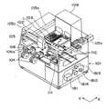
図2に上記電子部品実装機101を示す。電子部品実装機101における基本的な構造は、図15を参照して説明した従来の電子部品実装機50の構造と変わるものではないが、電子部品実装機101では詳細後述する制御装置181、及び電子部品認識装置1810を有する点が特徴の一つである。
上記電子部品実装機101は、大別して、当該電子部品実装機101への基板1の搬入、電子部品実装機101からの基板1の搬出を行う基板搬送装置102と、該基板搬送装置102の基板搬送路を挟み、例えば左、右両側に配置され、基板1へ実装する電子部品7の供給を行う部品供給装置104、108と、部品供給装置104、108から電子部品7を保持し基板1へ装着する装着ヘッド106と、装着ヘッド106が取り付けられ、互いに直交するX,Y方向へ上記装着ヘッド106を移動させるX,Yロボット105と、装着ヘッド106にて保持された電子部品7の保持姿勢を撮像する照明撮像装置110と、上述の各構成部分の動作制御を行う制御装置181とを備える。尚、制御装置181は、記憶部1811を有し、該記憶部1811には、少なくとも、部品供給装置104、108から供給される電子部品7の各部の寸法情報と、いずれの電子部品7を基板1上のいずれの実装位置へどのような順番で実装していくかを示す実装プログラムとが格納されている。又、制御装置181には、例えば実装動作に関する情報を作業者が入力するための操作盤111が接続されている。
【0011】
ここで、上記部品供給装置104は、上述した部品供給装置4と同様のリールタイプの部品供給装置であり、上記部品供給装置108は、上述した部品供給装置8と同様のトレイタイプの部品供給装置である。
上記装着ヘッド106には、本実施形態では吸着動作にて電子部品7の保持を行うノズル106aが、少なくとも1本設けられ、図1に示すように、装着ヘッド106内に備わり上記制御装置181にて動作制御されるノズル昇降装置1062にて、ノズル106aは、基板1の厚み方向に移動可能であり、これにより上記部品供給装置104、108からの電子部品7の保持動作、及び基板1上への電子部品7の実装動作が可能となる。さらに、装着ヘッド106内には、図1に示すように、上記吸着動作用の吸引装置1061が備わるとともに、ノズル106aをその軸回り方向へ回転させる回転装置1063が備わる。該回転装置1063は、ノズル106aに保持された電子部品7の保持姿勢と、基板1上の実装位置における真の実装姿勢とにおける、上記軸回り方向のズレを補正するために、ノズル106aの上記回転を行う。上記吸引装置1061及び回転装置1063は、制御装置181に接続され、制御装置181にてそれぞれ吸引動作及び回転角度が制御される。
尚、上記基板1上の実装位置における真の実装姿勢とは、当該電子部品実装機101に設定されている座標原点を基準として表した、基板1上の実装位置における実装姿勢であり、言わば設計上における実装姿勢である。
【0012】
上記X,Yロボット105は、上記装着ヘッド106を有し、上述のX,Yロボット5と同様に、Y方向移動部105yとX方向移動部105xとを有する。尚、これらY方向移動部105y及びX方向移動部105xは、それぞれ上記制御装置181にてその移動量が制御される。
【0013】
上記照明撮像装置110は、図1、図3及び図4に示すように、上記ノズル106aに保持された電子部品7の保持姿勢を撮像する、例えばCCDカメラを有する撮像装置1101と、256階調にて明るさの変更が可能であり本実施形態ではハロゲンランプにてなる光源を有し、上記撮像動作のときにノズル106aに保持された電子部品7を照明する照明装置1102とを有する。尚、当該電子部品実装機101では、上記照明撮像装置110は、図3に示すように、いわゆる反射式の照明装置1102を有する。即ち、撮像装置1101への入射光入口の近傍において、撮像装置1101を中心としてその周辺部分に、上記照明装置1102が配置され、該照明装置1102から照射された光は、上記ノズル106aに保持されている電子部品7のボディー部7a及び電極7b、並びにノズル106aに設けた反射板に当たり、主に、上記ボディー部7a及び電極7bから反射した光が入射光として撮像装置1101へ入射する。尚、上記反射板は、上記電極7bがより鮮明に撮像されるような色、例えば黒色にて塗装された板材である。
【0014】
又、上述したように、従来の部品認識装置10では電子部品7における明るさが変化することに起因して、実装位置に正確に電子部品を実装できない場合や、認識率及び生産性の低下を来す場合があった。これらの問題点を解決するために、本実施形態では、ノズル106aに保持された電子部品7の保持姿勢をより明確に認識することで、上記保持姿勢と基板1上の実装位置における上記実装姿勢とのズレ量をより正確に求めることを可能とし、その結果、基板1上の実装位置へ電子部品7を正確に実装可能とし上記認識率及び生産性の向上を可能とする。ここで、従来に比べて上記保持姿勢をより明確に認識可能とするため、本実施形態では、部品認識のための明るさの最適化を図る。該最適化が図れるように、本実施形態では以下のように構成している。
【0015】
即ち、上記照明装置1102には、例えば上記光源への電力供給を制御することで上記電子部品7に対する明るさを変化させる明るさ変更装置1812を接続し、撮像装置1101には、該撮像装置1101における上記CCDカメラのゲインを変化させるゲイン変更装置1813を接続するとともに、上記電子部品7を撮像して得られる撮像情報が供給され該撮像情報に基づいて上記明るさ変更装置1812及びゲイン変更装置1813の動作制御を行う認識制御部1814を接続している。
【0016】
ここで、上記認識制御部1814は、上記撮像装置1101にて撮像された電子部品7の撮像情報における解像度を向上させるため、本実施形態では、上記保持姿勢の撮像情報を元に、上記明るさ変更装置1812を制御して電子部品7における明るさを改善し、該改善により、照明装置1102によって照らされた電子部品7の電極7bにおける明るさ、又は電極7bの撮像情報に基づく寸法を実装精度向上領域に設定させる。ここで、上記実装精度向上領域とは、上記ノズル106aに保持されている電子部品7の上記保持姿勢と、基板1上の実装位置における上記実装姿勢とのズレを求めるときに上記保持姿勢の上記撮像情報における解像度を向上させて上記ズレを許容範囲内に設定可能とする上記明るさ又は寸法の領域である。
尚、上記撮像装置1101、照明装置1102、明るさ変更装置1812、ゲイン変更装置1813、及び認識制御部1814にて電子部品認識装置1810を構成する。又、上記認識制御部1814と上記制御装置181とは接続されている。
【0017】
本実施形態では上述のように上記認識制御部1814は、上記撮像装置1101にて撮像された電子部品7の撮像情報における解像度を向上させるため、上記明るさ変更装置1812を制御したが、これに限定されず、上記ゲイン変更装置1813を制御してもよい。さらには、明るさ変更装置1812及びゲイン変更装置1813の両方を制御するようにしてもよい。
【0018】
このように構成された上記電子部品認識装置1810は以下のように動作する。
図5に示すように、ステップ(図5では「S」にて示す)1にて、電子部品7の明るさ調整を行うことが指示され、ステップ2では、X,Yロボット105を駆動して装着ヘッド106のノズル106aにて、例えば部品供給装置104から電子部品7を保持する。次のステップ3では、装着ヘッド106のノズル106aに保持されている電子部品7を、X,Yロボット105を駆動して照明撮像装置110の上方へ移動し、ステップ4にて、照明装置1102から光を電子部品7へあて、電子部品7の認識動作を行う。
【0019】
このとき、上記照明装置1102から発した光の、主に、電子部品7のボディー部7a及び電極7bにおける反射光が撮像装置1101に入る。撮像装置1101に入った光は、上記CCDカメラを構成するCCD素子にて電気信号に変換され、撮像情報として認識制御部1814へ送られる。認識制御部1814では、上記電気信号にてなる上記撮像情報を画像処理して上記ノズル106aに保持されている電子部品7の輪郭若しくは明るさ、又は、輪郭及び明るさを求める。ステップ5では、上記撮像情報、つまり電子部品7の上記輪郭が明瞭か否か、上記明るさが十分か否かが判断される。
このとき、上記輪郭若しくは明るさ、又は、輪郭及び明るさが不明瞭なときには、以下に説明する種々の照度最適化手法の少なくとも一つを使用して、より明確に上記輪郭若しくは明るさ、又は、輪郭及び明るさが求まるように、認識制御部1814は上記明るさ変更装置1812を制御し、変更された明るさによって撮像された上記保持姿勢の撮像情報が認識制御部1814にフィードバックされる。このようなフィードバック制御動作を繰り返すことで、上記輪郭が最も明確になる明るさ、又は認識動作に十分な明るさが得られる。
【0020】
認識制御部1814は、このように最適化された明るさに関する情報を上記ゲイン変更装置1813にも送出する。よって、ゲイン変更装置1813は、上記最適化された明るさに対応した最適ゲインにて上記撮像装置1101に撮像動作を行わせる。
よって、認識制御部1814は、最適化された明るさで、かつ上記最適ゲインにて撮像され得られた電子部品7の輪郭から電子部品7の中心位置を求める。このようにして求まる上記中心位置の精度は、従来に比べて高くなる。求まった上記中心位置の情報は、認識制御部1814から制御装置181へ送出される。
【0021】
このようにして求まった、上記最適化された明るさ及び最適ゲインに関する情報は、撮像した電子部品7と関連付けて、制御装置181の記憶部1811に記憶される(ステップ6)。
尚、より明確に上記輪郭を求めるために、ステップ7では、上述したようにゲイン変更装置1813を、又は、明るさ変更装置1812及びゲイン変更装置1813の両方を制御するようにしてもよい。
【0022】
そして、上記制御装置181では、供給された上記中心位置の情報と、当該電子部品実装機101に設定されている上記座標原点を基準としたときの絶対位置であって、ノズル106aに保持されて電子部品7が照明撮像装置110の上方に配置されたときのノズル106aにおける中心の絶対位置の情報とのズレ量を求める。このようにして求まる上記ズレ量は、電子部品7の中心位置の精度が従来に比べて高い分、従来に比べて高い精度にて求めることができる。
尚、ノズル106aにて電子部品7を保持するとき、設計上、ノズル106aの上記中心と、電子部品7の上記中心位置とが一致するように、ノズル106aは電子部品7を保持可能である。又、ノズル106aに保持されて電子部品7が照明撮像装置110の上方に配置されたときのノズル106aにおける中心の上記絶対位置の情報は、予め制御装置181の上記記憶部1811に記憶されている。
【0023】
以下には、上述した、種々の照度最適化手法について説明する。尚、照度最適化手法は以下のものに限定されるものではなく、当業者が通常行っている公知の種々の手法を使用することもできる。
第1の照度最適化手法では、図6ないし図8に示すように、制御装置181の記憶部1811に予め格納された電子部品7の真の寸法値と、上記撮像情報に基づき認識制御部1814にて求めた電子部品7の寸法値とを比較して、上記撮像情報に基づく寸法値が上記実装精度向上領域内に含まれるように、明るさ変更装置1812に対してフィードバック制御し電子部品7に対する明るさを調整する。
【0024】
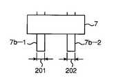
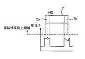
尚、図6には、一部の電極7bの図示を省略した、撮像される電子部品7が示されている。ここで、電極7bの延在方向及び厚み方向に直交する幅寸法であって、電極7b−1の幅寸法を符号201にて、電極7b−2の幅寸法を符号202にて表す。図7には、明るさ変更装置1812を制御する前において、図6に示す電子部品7を撮像したときの撮像情報が示されている。ここで、上記電極7b−1について撮像情報に基づいた上記幅寸法を符号203にて示し、上記電極7b−2について撮像情報に基づいた上記幅寸法を符号204にて示す。図8には、明るさ変更装置1812を制御した後において図6に示す電子部品7を撮像したときの撮像情報が示されている。ここで、上記電極7b−1について撮像情報に基づいた上記幅寸法を符号205にて示し、上記電極7b−2について撮像情報に基づいた上記幅寸法を符号206にて示す。
【0025】
具体的に説明すると、認識制御部1814は、まず、上記幅寸法203と上記幅寸法201とを比較し、上記幅寸法204と上記幅寸法202とを比較する。この結果、上記幅寸法203及び幅寸法204は上記実装精度向上領域内に含まれないと、認識制御部1814は判断し、明るさ変更装置1812を制御して照明装置1102の光源の明るさを変化させる。
そして明るさ変更装置1812の制御後において、認識制御部1814は上記幅寸法205、206と、上記幅寸法201、202とを比較し、上記幅寸法205、206が上記実装精度向上領域に含まれるか否かを判断する。このようにして上記幅寸法205、206が上記実装精度向上領域に含まれるまで、認識制御部1814及び明るさ変更装置1812がフィードバック制御される。
尚、上述のような実装精度向上領域という概念を用いずに、上記幅寸法205、206が上記幅寸法201、202に最も近付くように、上記明るさ変更装置1812を制御してもよい。
又、本実施形態では、上述のように複数の電極7bの幅寸法について比較動作を行うが、いずれか一つの電極7bのみについて比較動作を行っても良い。
【0026】
又、上述のように明るさ変更装置1812が制御され電子部品7に対する明るさが適切になるに従って、図7及び図8に示すように、電極7b−1,7b−2における明るさ、いわゆる照度のレベルが上昇する。この性質を利用して、電極7bにおける照度が実装精度向上領域に含まれるまで、認識制御部1814及び明るさ変更装置1812をフィードバック制御するように構成することもできる。
【0027】
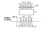
第2の照度最適化手法では、図9に示すように、撮像された電子部品7の複数の電極7bについて同位置におけるそれぞれの明るさがすべて実装精度向上領域に存在するように、認識制御部1814は上記明るさ変更装置1812を制御する。
具体的に説明すると、図9に示す各電極7b−3、7b−4、7b−5、7b−6、7b−7について、仮想の直線216が通過している同位置の明るさがすべて実装精度向上領域に存在するように、認識制御部1814は上記明るさ変更装置1812を制御する。ここで、この第2の照度最適化手法の場合、上記実装精度向上領域とは、上記電極7bにおける明るさが基準値を超える領域である。
尚、本実施形態では、上述のように各電極7b−3、7b−4等における同位置の明るさがすべて実装精度向上領域に存在するように、上記明るさ変更装置1812を制御したが、これに限定されるものではない。即ち、上記制御のために着目している電極7bの数の、例えば過半数、若しくは8割以上、等の数の電極7bの上記同位置における明るさが実装精度向上領域に存在するように上記明るさ変更装置1812を制御するようにしてもよい。
【0028】
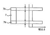
第3の照度最適化手法では、図10に示すように、電極7bの複数箇所における明るさの平均値が実装精度向上領域に存在するように、認識制御部1814は上記明るさ変更装置1812を制御する。
具体的に説明すると、図10に示す電極7b−8の複数の場所221における明るさの平均値が実装精度向上領域に存在するように、認識制御部1814は上記明るさ変更装置1812を制御する。ここで、この第3の照度最適化手法の場合、上記実装精度向上領域とは、上記場所221の明るさの平均値が基準値を超える領域である。
尚、本実施形態では、上述のように一つの電極7b−8について複数の場所221の明るさを使用したが、これに限定するものではなく、例えば各電極7b毎に一つずつ明るさ測定場所を設定してもよいし、各電極7b毎に複数の明るさ測定場所を設定してもよい。
【0029】
第4の照度最適化手法では、基板1上の所定の実装位置へ正確に電子部品7が実装された場合における、当該電子部品7の撮像情報内の電極7bにおける明るさ情報で、種々の形態の電子部品におけるいままでに得られた正常な明るさ情報と、検査対象である電子部品7の撮像情報内における電極7bの明るさ情報とを比較し、検査対象である電子部品7の電極7bの明るさのレベルが上記正常な明るさ情報に基づいて設定した実装精度向上領域に存在するように、認識制御部1814は上記明るさ変更装置1812を制御する。
具体的に説明すると、制御装置181の記憶部1811に、予め、種々の形態の電子部品について、いままでに得られた、図14に示すような正常な明るさ情報を格納しておく。そして、ノズル106aに保持された電子部品7と同じ電子部品における上記正常な明るさ情報と、ノズル106aに保持された電子部品7を撮像して得られた、例えば図13に示すような当該電子部品7の電極7bの明るさとを認識制御部1814は比較し、当該電子部品7の電極7bの明るさのレベルが上記実装精度向上領域に存在するように、上記明るさ変更装置1812を制御する。
尚、このとき、上記正常な明るさ情報とともに、撮像時の電子部品における明るさの情報、若しくは照明装置1102の輝度の情報を記憶しておくことで、新たな電子部品7を撮像するに当たり、認識制御部1814が明るさ変更装置1812を制御するとき、上述のような比較動作を行うことなく、上記明るさの情報、若しくは上記輝度の情報を参照して、明るさ変更装置1812を制御するようにしてもよい。
【0030】
又、電子部品7によっては、撮像されるときの、照明撮像装置110に対するノズル106aの軸回り方向における電子部品7の回転角度により、電子部品7の認識の良否が変化する場合がある。よって、第5の照度最適化手法では、図11、12に示すように、ノズル106aに保持された電子部品7を、上記軸回り方向へー定角度毎に変化させながら撮像を行い、上述の第1〜第4のいずれかの照度最適化手法を用いて、認識制御部1814は明るさ変更装置1812を制御して、各回転動作毎の認識結果を得る。そして、これらの認識結果について、制御装置181は、ノズル106aにおける電子部品7の上記保持姿勢と基板1上の実装位置における上記実装姿勢とのズレ量が最も小さくなる場合を選択し、その場合に対応した回転角度を記憶する。よって、当該電子部品7については、記憶した回転角度にノズル106aを回転させて認識動作を行うことになる。
尚、このように撮像時に電子部品7を回転した場合、基板1への実装時には上記回転角度を考慮する必要があるので、最適な認識が行われたときの角度情報が制御装置181の記憶部1811へ格納される。よって、実装時には、制御装置181は、記憶部1811から上記角度情報を読み出し、該角度を考慮した実装制御を行う。
【0031】
上記第1〜第5の照度最適化手法を実行して得られた、照明装置1102の光源の最適な明るさの情報は、各種の電子部品7毎に、制御装置181の記憶部1811に自動的に記憶される。又、作業者が例えば経験から得た最適な明るさの情報を、作業者が操作盤111から直接、制御装置181へ入力することも可能である。このように、制御装置181へ供給された上記最適な明るさの情報は、以後の部品認識動作に活用される。
【0032】
上記第1〜第5の照度最適化手法において、上述したように明るさ変更装置1812に代えて、若しくは明るさ変更装置1812とともに、ゲイン変更装置1813に対して制御を施しても良い。この場合、撮像装置1101に備わるカメラのゲインを上げると、当該カメラ内部のノイズも同時に上がるというデメリットがある。又、照明装置1102の光源の明るさを増すと上記カメラの感度が飽和し、電極7bの上記幅寸法が1の値よりも太くなる現象(ブルーミング)がある。
そこで、本実施形態の電子部品認識装置1810及び制御装置181では、上記ブルーミングのチェック機能を搭載している。つまり、電子部品7の電極7bについて撮像情報から求めた上記幅寸法値が、設定した基準値を超えたときには照明装置1102の光源の明るさを1段階下げ、かつ上記カメラのゲインを1段階上げることにより、上記ブルーミングの補正処理を行う。
本実施形態の電子部品認識装置1810及び制御装置181では、照明装置1102の光源の明るさを上記基準値に対して飽和状態になるまで調整し、その上で、より最適な撮像情報を得るように、上記カメラゲインによる微調整を自動的に行う。
【0033】
以上説明したような電子部品認識装置1810を有する電子部品実装機101では、以下のように実装動作が行われる。
即ち、図5を参照して上述したように、上記ステップ1〜ステップ6の動作を行うことで、基板1上に実装される電子部品7について適切な、本実施形態では、照明装置1102の光源の明るさが設定され、その設定値が電子部品7と対応付けて上記記憶部1811に記憶されていく。
撮像後、ノズル106aに保持された電子部品7は、制御装置181にて動作制御されることで移動量が制御されるX、Yロボット105にて基板1上の上記実装位置へ運ばれ、かつ必要に応じてノズル106aがその軸回り方向へ回転される。このとき、上記移動量及び回転角度量は、電子部品認識装置1810の認識制御部1814から制御装置181に送出された上記撮像情報に基づいて、上記実装位置への電子部品7の実装精度を向上させるように制御装置181が求めた値である。
【0034】
このように本実施形態の電子部品実装機101によれば、電子部品7の認識動作時における照明装置1102の光源の明るさが自動調整されることから、従来に比べてより正確に部品保持姿勢を認識することができ、又、電子部品7の各電極7bの寸法のバラツキや、電極7bの位置のバラツキ等が存在する場合であっても従来に比べてより正確に部品保持姿勢を認識することができる。したがって、基板1上の実装位置へ電子部品7を移動させるときの移動補正量が従来に比べて正確になる。よって、従来に比べて上記実装位置へより正確に電子部品7を実装可能であり、実装位置に関係する不具合が減少することから実装済み基板の生産性の向上を図ることもできる。
【0035】
又、電子部品認識装置1810を用いることで、基板1のそりの影響や、それぞれの電子部品7のばらつきの影響を補償するための圧力センサなどのハード的な構成要素を使用することなく、最適な実装を行うことができる。このように電子部品認識装置1810を用いることは、電子部品実装機101の寿命、コストに対しても効果を奏する。
【0036】
尚、上述した実装動作では、製品となる回路基板へ電子部品7を実装しながらその都度、照明装置1102の光源の明るさを調整する旨の説明をした。しかしながら、実際的には以下の構成を採るのが好ましい。
予め求めた、実装される各種の電子部品7毎における照明装置1102の光源の適切な明るさの情報が、製品となる回路基板への実装動作開始前に、制御装置181へ供給される。又、上述のように制御装置181には上記実装プログラムが供給されるので、制御装置181より制御される上記認識制御部1814は、これらの上記明るさの情報と、実装プログラムとに基づいて、ノズル106aに保持され照明撮像装置110上に配置された各電子部品7に対応して照明装置1102の光源を適切な明るさに制御する。
このような動作により、様々な種類の電子部品7に対する対応力が増し、生産性を向上させることができる。
【0037】
又、本実施形態の電子部品実装機101は、以下のような変形例として構成することもできる。
本実施形態における照明撮像装置110は、上述のように、いわゆる反射式の照明装置1102を有するが、図4に示すような、いわゆる透過式の照明装置1103を有する照明撮像装置も知られている。このような透過式の照明撮像装置では、ノズル106aに保持された電子部品7が撮像装置1101の上方に配置されたとき、例えばLED(発光ダイオード)を光源として備えたシャッター1103が、シャッター駆動装置1104にて、ノズル106aを左右より挟むように移動してくる。このとき、図4に示すように電子部品7が撮像装置1101とシャッター1103との間に位置し、かつシャッター1103の上記LEDの発光面が撮像装置1101に対向するように、シャッター1103は配置される。
【0038】
一方、最適な撮像情報を得るために、電子部品7の種類に応じて、上記反射型又は上記透過型が好ましいのか、適正がある。
そこで、上記反射型の照明装置1102及び上記透過型の照明装置1103の両方を備えた電子部品認識装置を構成することもできる。このような電子部品認識装置では、一つの電子部品7に対して両方の照明装置1102、1103を順次使用してそれぞれ撮像を行い、上述した第1〜第5の照度最適化手法の少なくとも一つを使用してそれぞれの撮像情報を得る。そして、上記認識制御部1814にて、それぞれの上記撮像情報の内、上記実装精度向上領域に含まれたものの中で最適な撮像情報を提供した場合における光を提供した上記反射型又は透過型の一方を選択する。
よって、このように二つの照明装置1102、1103を備えた電子部品認識装置では、いずれか一方の照明装置を備えた電子部品認識装置に比べて、より高い精度で電子部品7の上記保持姿勢の認識が行えることから、基板1上の実装位置に、より正確に電子部品を実装可能な場合があり、認識率及び生産性の向上を図ることができる場合がある。
【0039】
【発明の効果】
以上、詳述したように、本発明の第1態様の電子部品認識装置、及び第2態様の電子部品認識方法、さらには本発明の第3態様の電子部品実装機によれば、撮像装置、照明装置、明るさ変更装置、及び認識制御部を備え、上記撮像装置にて撮像された電子部品の撮像情報における解像度を向上させるため、上記認識制御部にて上記明るさ変更装置を制御して、上記電子部品における明るさを適切に設定するようにした。したがって、部品保持部材に保持された電子部品の保持姿勢の認識を従来に比べてより高精度にて行うことができる。よって、上記保持姿勢と、被装着体上の実装位置における実装姿勢とのズレを従来に比べてより正確に求めることができ、上記実装位置へ電子部品を移動させるときの移動補正量を従来に比べてより高い精度にて求めることができる。よって、従来に比べて上記実装位置へより正確に電子部品を実装可能であり、実装位置に関係する不具合が減少することから実装済み被装着体の生産性の向上を図ることもできる。
【図面の簡単な説明】
【図1】 本発明の実施形態の電子部品認識装置の構成を示すブロック図である。
【図2】 図1の電子部品認識装置を備えた、本発明の実施形態における電子部品実装機の斜視図である。
【図3】 図1の電子部品認識装置に備わる反射式の照明装置及び撮像装置における撮像動作を説明するための図である。
【図4】 図1の電子部品認識装置の変形例における透過式の照明装置及び撮像装置での撮像動作を説明するための図である。
【図5】 図1の電子部品認識装置を用いた部品認識動作を説明するためのフローチャートである。
【図6】 図1の電子部品認識装置にて実行される第1の照度最適化手法にて撮像される電子部品の平面図である。
【図7】 図6に示す電子部品について、明るさの制御を行う前に撮像した場合における電極の明るさを説明するための図である。
【図8】 図6に示す電子部品について、明るさの制御を行った後に撮像した場合における電極の明るさを説明するための図である。
【図9】 図1の電子部品認識装置にて実行される第2の照度最適化手法にて電子部品を撮像した場合における電極の明るさを説明するための図である。
【図10】 図1の電子部品認識装置にて実行される第3の照度最適化手法を説明するための図である。
【図11】 図1の電子部品認識装置にて実行される第5の照度最適化手法を説明するための図である。
【図12】 図1の電子部品認識装置にて実行される第5の照度最適化手法を説明するための図であって、図11に示す電子部品を回転させた後の状態を示す図である。
【図13】 図1の電子部品認識装置にて実行される第4の照度最適化手法を説明するための図であって、撮像が不適切な場合を示す図である。
【図14】 図1の電子部品認識装置にて実行される第4の照度最適化手法を説明するための図であって、撮像が適切な場合を示す図である。
【図15】 従来の電子部品実装機の斜視図である。
【符号の説明】
1…基板、7…電子部品、7b…電極、
101…電子部品実装機、106…装着ヘッド、106a…ノズル、
181…制御装置、
1101…撮像装置、1102…照明装置、1103…照明装置、
1810…電子部品認識装置、1811…記憶部、1812…明るさ変更装置、
1813…ゲイン変更装置、1814…認識制御部。[0001]
BACKGROUND OF THE INVENTION
The present invention relates to an electronic component recognition device that captures and recognizes an electronic component mounted on a mounted body such as a substrate, an electronic component recognition method executed by the electronic component recognition device, and the electronic component recognition device. The present invention relates to an equipped electronic component mounting machine.
[0002]
[Prior art]
2. Description of the Related Art Conventionally, an electronic component mounting machine that mounts electronic components at predetermined positions on a substrate such as a printed circuit board has a configuration as shown in FIG. That is, the conventional electronic
[0003]
Here, the
[0004]
The conventional electronic
The
The
[0005]
[Problems to be solved by the invention]
However, when the
The present invention has been made to solve such problems, and by improving the accuracy of component recognition, it is possible to accurately mount electronic components at the mounting position, and the recognition rate and productivity can be improved. Another object is to provide an electronic component recognition apparatus and method, and an electronic component mounter.
[0006]
[Means for Solving the Problems]
The electronic component recognition apparatus according to the first aspect of the present invention includes a deviation between a holding posture of the electronic component held by the component holding member and a mounting posture at the mounting position before being mounted at the mounting position on the mounted body. An electronic component recognition apparatus that images the holding posture, which is used to improve mounting accuracy of the electronic component at the mounting position by correcting
An imaging device for imaging the holding posture of the electronic component held by the component holding member;
An illumination device for illuminating the electronic component for imaging the holding posture by the imaging device;
A brightness changing device that changes the brightness of the electronic component with respect to the lighting device;
In order to improve the resolution in the imaging information of the electronic component imaged by the imaging device, the brightness changing device is controlled so that the power of the electronic component illuminated by the illumination device is increased.very Dimensions based on imaging informationabout ,The error with the actual dimensions of the electrode can be set within the allowable range. Recognition control to be set in the mounting accuracy improvement area, which is the dimension areaDepartment and ,
It is provided with.
[0007]
The electronic component recognition method according to the second aspect of the present invention corrects the deviation between the holding posture of the electronic component before being mounted on the mounting position on the mounted body and the mounting posture at the mounting position. An electronic component recognition method for recognizing the holding posture for obtaining the deviation by imaging when improving the mounting accuracy of the electronic component at a mounting position,
In order to improve the resolution in the imaging information of the electronic component when imaging the electronic component, the brightness of the electronic component when imaging the electronic component is controlled.And The above electronic components are illuminatedFor the dimensions based on the imaging information of the poles, the error from the actual dimensions of the electrodes can be set within an allowable range. Set in the mounting accuracy improvement area, which is the dimension area,
It is characterized by that.
[0008]
An electronic component mounting machine according to the third aspect of the present invention includes the electronic component recognition apparatus according to the first aspect,
A control device that obtains the deviation between the holding posture of the electronic component imaged based on the brightness of the electronic component controlled by the recognition control unit and the mounting posture at the mounting position;
A mounting head for mounting an electronic component having a component holding member to a mounting position on a mounted body, wherein the control device causes the component holding member to be mounted according to the deviation obtained by the control device. A mounting head whose operation is controlled;
A moving device that has the mounting head and moves the mounting head, wherein the moving amount of the mounting head is controlled by the control device in accordance with the displacement obtained by the control device; and
It is provided with.
[0009]
DETAILED DESCRIPTION OF THE INVENTION
An electronic component recognition device, an electronic component recognition method executed by the electronic component recognition device, and an electronic component mounter including the electronic component recognition device, which are embodiments of the present invention, will be described below with reference to the drawings. explain. In addition, in each figure, the same code | symbol is attached | subjected about the same component. Further, as an example of fulfilling the function of the “component holding member” described in the “Means for Solving the Problems” section, the
[0010]
First, the electronic component mounting machine of this embodiment will be described.
FIG. 2 shows the electronic
The electronic
[0011]
Here, the
In the present embodiment, the mounting
Note that the true mounting posture at the mounting position on the
[0012]
The X and
[0013]
As shown in FIGS. 1, 3, and 4, the
[0014]
In addition, as described above, in the conventional
[0015]
That is, the
[0016]
Here, in order to improve the resolution in the imaging information of the
The
[0017]
In this embodiment, as described above, the
[0018]
The electronic
As shown in FIG. 5, in step (indicated by “S” in FIG. 5) 1 is instructed to adjust the brightness of the
[0019]
At this time, reflected light of the light emitted from the illuminating
At this time, when the outline or brightness, or the outline and brightness are unclear, use at least one of various illuminance optimization methods described below to clarify the outline or brightness, or The
[0020]
The
Therefore, the
[0021]
Information on the optimized brightness and optimum gain obtained in this way is stored in the
In order to obtain the contour more clearly, in
[0022]
In the
When the
[0023]
Below, the various illumination intensity optimization methods mentioned above are demonstrated. The illuminance optimization method is not limited to the following, and various known methods that are commonly performed by those skilled in the art can also be used.
In the first illuminance optimization method, as shown in FIGS. 6 to 8, the
[0024]
FIG. 6 shows the
[0025]
Specifically, the
After the control of the
Note that the
In the present embodiment, the comparison operation is performed for the width dimensions of the plurality of
[0026]
Further, as shown in FIGS. 7 and 8, the brightness at the
[0027]
In the second illuminance optimization method, as shown in FIG. 9, the recognition control unit is configured so that all the brightness at the same position of the plurality of
More specifically, for each of the
In this embodiment, as described above, the
[0028]
In the third illuminance optimization method, as shown in FIG. 10, the
More specifically, the
In the present embodiment, the brightness of the plurality of
[0029]
In the fourth illuminance optimization method, when the
More specifically, normal brightness information as shown in FIG. 14 obtained for various types of electronic components is stored in the
At this time, by storing information on the brightness of the electronic component at the time of imaging, or information on the luminance of the
[0030]
In addition, depending on the
In addition, when the
[0031]
Information on the optimum brightness of the light source of the
[0032]
In the first to fifth illuminance optimization methods, the
Therefore, the electronic
In the electronic
[0033]
In the
That is, as described above with reference to FIG. 5, the light source of the
After the imaging, the
[0034]
As described above, according to the electronic
[0035]
In addition, by using the electronic
[0036]
In the mounting operation described above, it has been described that the brightness of the light source of the
Information on the appropriate brightness of the light source of the
With such an operation, the ability to cope with various types of
[0037]
Moreover, the electronic
The
[0038]
On the other hand, in order to obtain optimal imaging information, the reflection type or the transmission type is preferable or appropriate depending on the type of the
Therefore, an electronic component recognition device including both the
Therefore, in the electronic component recognition device including the two
[0039]
【The invention's effect】
As described above in detail, according to the electronic component recognition apparatus of the first aspect of the present invention, the electronic component recognition method of the second aspect, and the electronic component mounter of the third aspect of the present invention, the imaging apparatus, An illumination device, a brightness change device, and a recognition control unit are provided, and the brightness control device is controlled by the recognition control unit in order to improve the resolution in the imaging information of the electronic component imaged by the imaging device. The brightness of the electronic component is set appropriately. Accordingly, it is possible to recognize the holding posture of the electronic component held by the component holding member with higher accuracy than in the past. Therefore, the deviation between the holding posture and the mounting posture at the mounting position on the mounted body can be determined more accurately than in the past, and the amount of movement correction when moving the electronic component to the mounting position is conventionally It can be determined with higher accuracy. Therefore, it is possible to mount the electronic component more accurately at the mounting position as compared with the conventional case, and since defects related to the mounting position are reduced, it is possible to improve the productivity of the mounted body to be mounted.
[Brief description of the drawings]
FIG. 1 is a block diagram showing a configuration of an electronic component recognition apparatus according to an embodiment of the present invention.
2 is a perspective view of an electronic component mounting machine according to an embodiment of the present invention that includes the electronic component recognition apparatus of FIG. 1; FIG.
3 is a diagram for explaining an imaging operation in a reflective illumination device and an imaging device provided in the electronic component recognition device in FIG. 1; FIG.
FIG. 4 is a diagram for explaining an imaging operation in a transmissive illumination device and an imaging device in a modification of the electronic component recognition device in FIG. 1;
FIG. 5 is a flowchart for explaining a component recognition operation using the electronic component recognition apparatus of FIG. 1;
6 is a plan view of an electronic component imaged by a first illuminance optimization method executed by the electronic component recognition apparatus in FIG. 1. FIG.
7 is a diagram for explaining the brightness of an electrode when the electronic component shown in FIG. 6 is imaged before brightness control is performed.
8 is a diagram for explaining the brightness of an electrode when the electronic component shown in FIG. 6 is imaged after brightness control is performed.
FIG. 9 is a diagram for explaining the brightness of an electrode when an electronic component is imaged by a second illuminance optimization method executed by the electronic component recognition apparatus of FIG. 1;
10 is a diagram for explaining a third illuminance optimization technique executed by the electronic component recognition apparatus in FIG. 1; FIG.
FIG. 11 is a diagram for explaining a fifth illuminance optimization technique executed by the electronic component recognition apparatus in FIG. 1;
12 is a diagram for explaining a fifth illuminance optimization technique executed by the electronic component recognition apparatus of FIG. 1 and shows a state after the electronic component shown in FIG. 11 is rotated. is there.
13 is a diagram for explaining a fourth illuminance optimization method executed by the electronic component recognition apparatus in FIG. 1, and is a diagram illustrating a case where imaging is inappropriate. FIG.
14 is a diagram for explaining a fourth illuminance optimization technique executed by the electronic component recognition apparatus in FIG. 1, and is a diagram illustrating a case where imaging is appropriate. FIG.
FIG. 15 is a perspective view of a conventional electronic component mounting machine.
[Explanation of symbols]
DESCRIPTION OF
101 ... Electronic component mounting machine, 106 ... Mounting head, 106a ... Nozzle,
181 ... Control device,
1101 ... Imaging device, 1102 ... Illumination device, 1103 ... Illumination device,
1810 ... Electronic component recognition device, 1811 ... Storage unit, 1812 ... Brightness change device,
1813: Gain changing device, 1814: Recognition control unit.
Claims (6)
Translated fromJapanese上記部品保持部材に保持された電子部品の上記保持姿勢を撮像する撮像装置と、
上記撮像装置による上記保持姿勢の撮像のため上記電子部品を照明する照明装置と、
上記照明装置に対して上記電子部品に対する明るさを変化させる明るさ変更装置と、
上記撮像装置にて撮像された上記電子部品の撮像情報における解像度を向上させるため、上記明るさ変更装置を制御して、上記照明装置によって照らされた上記電子部品の電極の撮像情報に基づく寸法について、上記電極の実寸法との誤差を許容範囲内に設定可能とする寸法の領域である実装精度向上領域に設定させる認識制御部と、
を備えたことを特徴とする電子部品認識装置。Before being mounted to the mounting positionon the mountingmember, the above and holding postureof the electroniccomponent held bythe component holdingmember, into the mounting position by correcting the displacement between the mounting posture at the mounting position An electronic component recognition device for imaging the holding posture, which is used to improve mounting accuracy of electronic components,
An imagingequipment for imaging the holding posture of the electronic component held on the component holding member,
And lightingequipment for illuminating the electronic part for imaging of the holding position by the imaging device,
And brightness changeequipment for changing the brightness for the electronic component relative to the illuminating device,
To improve the resolution in the imaging information of the electronic component picked up by the imaging device, and controls the brightness changing device, based on the imaging information of the electronic components of theelectrodes illuminated by the illuminating device dimensionsAbout a recognition controlunit that setsan error with the actual dimension of the electrode within a mounting accuracy improvement area that is an area ofa dimension thatcan be set within an allowable range ;
An electronic component recognition device comprising:
上記実装精度向上領域は、上記電子部品の電極における実際の上記幅寸法に基づいて設定され、上記記憶部に記憶されている、請求項2記載の電子部品認識装置。The recognition control unit has a storage unit for storing the dimensions of the electronic components.
The electronic component recognition apparatus according toclaim 2, wherein the mounting accuracy improvement region is set based on the actual width dimension of the electrode of the electronic component and is stored in the storage unit.
上記認識制御部は、さらに上記ゲイン変更装置を制御して、上記電極における寸法を上記実装精度向上領域に設定させる、請求項1から3のいずれかに記載の電子部品認識装置。A gain changing device for changing the imaging sensitivity of the electronic component with respect to the imaging device;
The electronic component recognition device accordingto claim 1, wherein the recognition control unit further controls the gain changing device to set a dimension of the electrode in the mounting accuracy improvement region .
上記認識制御部にて制御された上記電子部品の明るさに基づいて撮像された上記電子部品の上記保持姿勢と、上記実装位置における実装姿勢との上記ズレを求める制御装置と、 A control device for determining the deviation between the holding posture of the electronic component imaged based on the brightness of the electronic component controlled by the recognition control unit and the mounting posture at the mounting position;
部品保持部材を有し保持している電子部品を被装着体上の実装位置へ実装する装着ヘッドであって、上記制御装置にて求めた上記ズレに応じて上記制御装置によって上記部品保持部材の動作が制御される装着ヘッドと、 A mounting head for mounting an electronic component having a component holding member to a mounting position on a mounted body, wherein the control device causes the component holding member to be mounted according to the deviation obtained by the control device. A mounting head whose operation is controlled;
上記装着ヘッドを有し該装着ヘッドを移動させる移動装置であって、上記制御装置にて求めた上記ズレに応じて上記制御装置によって上記装着ヘッドの移動量が制御される装着ヘッド移動装置と、 A moving device that has the mounting head and moves the mounting head, wherein the moving amount of the mounting head is controlled by the control device in accordance with the displacement obtained by the control device;
を備えたことを特徴とする電子部品実装機。An electronic component mounting machine comprising:
上記電子部品を撮像したときの上記電子部品の撮像情報における解像度を向上させるため、上記電子部品を撮像するときの上記電子部品における明るさを制御して、照らされた上記電子部品の電極の撮像情報に基づく寸法について、上記電極の実寸法との誤差を許容範囲内に設定可能とする寸法の領域である実装精度向上領域に設定する、 In order to improve the resolution in the imaging information of the electronic component when the electronic component is imaged, the brightness of the electronic component when the electronic component is imaged is controlled to image the illuminated electrode of the electronic component For the dimensions based on the information, set the error with the actual dimension of the electrode in the mounting accuracy improvement area, which is an area of a dimension that can be set within an allowable range.
ことを特徴とする電子部品認識方法。 The electronic component recognition method characterized by the above-mentioned.
Priority Applications (1)
| Application Number | Priority Date | Filing Date | Title |
|---|---|---|---|
| JP10122799AJP4326064B2 (en) | 1999-04-08 | 1999-04-08 | Electronic component recognition apparatus and method, and electronic component mounter equipped with electronic component recognition apparatus |
Applications Claiming Priority (1)
| Application Number | Priority Date | Filing Date | Title |
|---|---|---|---|
| JP10122799AJP4326064B2 (en) | 1999-04-08 | 1999-04-08 | Electronic component recognition apparatus and method, and electronic component mounter equipped with electronic component recognition apparatus |
Publications (2)
| Publication Number | Publication Date |
|---|---|
| JP2000294994A JP2000294994A (en) | 2000-10-20 |
| JP4326064B2true JP4326064B2 (en) | 2009-09-02 |
Family
ID=14295023
Family Applications (1)
| Application Number | Title | Priority Date | Filing Date |
|---|---|---|---|
| JP10122799AExpired - Fee RelatedJP4326064B2 (en) | 1999-04-08 | 1999-04-08 | Electronic component recognition apparatus and method, and electronic component mounter equipped with electronic component recognition apparatus |
Country Status (1)
| Country | Link |
|---|---|
| JP (1) | JP4326064B2 (en) |
Families Citing this family (1)
| Publication number | Priority date | Publication date | Assignee | Title |
|---|---|---|---|---|
| CN113276104B (en)* | 2020-02-19 | 2024-08-27 | 总督科技股份有限公司 | Method for calibrating the robotic arm of a wafer transfer mechanism |
- 1999
- 1999-04-08JPJP10122799Apatent/JP4326064B2/ennot_activeExpired - Fee Related
Also Published As
| Publication number | Publication date |
|---|---|
| JP2000294994A (en) | 2000-10-20 |
Similar Documents
| Publication | Publication Date | Title |
|---|---|---|
| EP0730397B1 (en) | Method for mounting components on a substrate and components mounting machine therefor | |
| JP2937785B2 (en) | Component state detection device for mounting machine | |
| WO2013005480A1 (en) | Laser height measuring device and component mounting machine | |
| US20040109172A1 (en) | Electronic parts mounting apparatus and method | |
| JP2015015357A (en) | Mounting device | |
| JP2001237596A (en) | Electronic component mounting apparatus and electronic component mounting method | |
| WO2021019610A1 (en) | Inspection device | |
| JP4308588B2 (en) | Surface mount machine | |
| JP4326064B2 (en) | Electronic component recognition apparatus and method, and electronic component mounter equipped with electronic component recognition apparatus | |
| JP3597611B2 (en) | Illumination device for mark recognition in mounting machine | |
| JPH11289199A (en) | Electronic parts recognizing device | |
| WO2018134862A1 (en) | Imaging device and surface mounting machine employing same | |
| JPH06310899A (en) | Reference point adjusting equipment for part recognizing equipment | |
| JP4715009B2 (en) | How to recognize workpiece reference marks | |
| JP2000307298A (en) | Method of mounting part | |
| JP6974101B2 (en) | Setting device and surface mounter | |
| JPH09321494A (en) | Illumination device for surface mounting machine | |
| JP4704218B2 (en) | Component recognition method, apparatus and surface mounter | |
| JPH1093300A (en) | Component mounting device | |
| JP4056572B2 (en) | Data creation apparatus and method, and electronic component mounting apparatus | |
| JPH08167800A (en) | Component mounting equipment | |
| JPH0451600A (en) | Mounting method for component | |
| JPH09246799A (en) | Device for recognizing part in mounter | |
| JP2008116274A (en) | 3D measuring device for electronic parts | |
| JP3914055B2 (en) | Component mounting equipment |
Legal Events
| Date | Code | Title | Description |
|---|---|---|---|
| A621 | Written request for application examination | Free format text:JAPANESE INTERMEDIATE CODE: A621 Effective date:20060330 | |
| A977 | Report on retrieval | Free format text:JAPANESE INTERMEDIATE CODE: A971007 Effective date:20080916 | |
| A131 | Notification of reasons for refusal | Free format text:JAPANESE INTERMEDIATE CODE: A131 Effective date:20081007 | |
| A521 | Written amendment | Free format text:JAPANESE INTERMEDIATE CODE: A523 Effective date:20081203 | |
| TRDD | Decision of grant or rejection written | ||
| A01 | Written decision to grant a patent or to grant a registration (utility model) | Free format text:JAPANESE INTERMEDIATE CODE: A01 Effective date:20090512 | |
| A01 | Written decision to grant a patent or to grant a registration (utility model) | Free format text:JAPANESE INTERMEDIATE CODE: A01 | |
| A61 | First payment of annual fees (during grant procedure) | Free format text:JAPANESE INTERMEDIATE CODE: A61 Effective date:20090609 | |
| FPAY | Renewal fee payment (event date is renewal date of database) | Free format text:PAYMENT UNTIL: 20120619 Year of fee payment:3 | |
| R150 | Certificate of patent or registration of utility model | Free format text:JAPANESE INTERMEDIATE CODE: R150 | |
| FPAY | Renewal fee payment (event date is renewal date of database) | Free format text:PAYMENT UNTIL: 20120619 Year of fee payment:3 | |
| FPAY | Renewal fee payment (event date is renewal date of database) | Free format text:PAYMENT UNTIL: 20130619 Year of fee payment:4 | |
| LAPS | Cancellation because of no payment of annual fees |