JP4325638B2 - Pulse wave measuring device - Google Patents
Pulse wave measuring deviceDownload PDFInfo
- Publication number
- JP4325638B2 JP4325638B2JP2006122206AJP2006122206AJP4325638B2JP 4325638 B2JP4325638 B2JP 4325638B2JP 2006122206 AJP2006122206 AJP 2006122206AJP 2006122206 AJP2006122206 AJP 2006122206AJP 4325638 B2JP4325638 B2JP 4325638B2
- Authority
- JP
- Japan
- Prior art keywords
- switch
- voltage
- pulse wave
- capacitor
- operational amplifier
- Prior art date
- Legal status (The legal status is an assumption and is not a legal conclusion. Google has not performed a legal analysis and makes no representation as to the accuracy of the status listed.)
- Expired - Fee Related
Links
- 239000003990capacitorSubstances0.000claimsdescription111
- 210000001367arteryAnatomy0.000claimsdescription34
- 238000001514detection methodMethods0.000claimsdescription14
- 238000003825pressingMethods0.000claimsdescription13
- 238000012546transferMethods0.000claimsdescription7
- 238000006243chemical reactionMethods0.000description57
- 238000005259measurementMethods0.000description52
- 238000000034methodMethods0.000description24
- 238000010586diagramMethods0.000description12
- 210000000707wristAnatomy0.000description10
- 238000012545processingMethods0.000description6
- 125000006850spacer groupChemical group0.000description4
- 238000004519manufacturing processMethods0.000description3
- 239000011159matrix materialSubstances0.000description3
- RYGMFSIKBFXOCR-UHFFFAOYSA-NCopperChemical compound[Cu]RYGMFSIKBFXOCR-UHFFFAOYSA-N0.000description2
- 239000011889copper foilSubstances0.000description2
- 239000004065semiconductorSubstances0.000description2
- 206010003210ArteriosclerosisDiseases0.000description1
- 230000001133accelerationEffects0.000description1
- 238000013459approachMethods0.000description1
- 230000004872arterial blood pressureEffects0.000description1
- 208000011775arteriosclerosis diseaseDiseases0.000description1
- 230000003416augmentationEffects0.000description1
- 239000000284extractSubstances0.000description1
- 210000000245forearmAnatomy0.000description1
- 239000004973liquid crystal related substanceSubstances0.000description1
- 230000007257malfunctionEffects0.000description1
- 238000000691measurement methodMethods0.000description1
- 229910044991metal oxideInorganic materials0.000description1
- 150000004706metal oxidesChemical class0.000description1
- 238000012986modificationMethods0.000description1
- 230000004048modificationEffects0.000description1
- 210000002321radial arteryAnatomy0.000description1
- 238000011160researchMethods0.000description1
- 230000000630rising effectEffects0.000description1
- 230000035945sensitivityEffects0.000description1
- 229920002379silicone rubberPolymers0.000description1
- 239000007787solidSubstances0.000description1
- 238000012360testing methodMethods0.000description1
Images


Classifications
- G—PHYSICS
- G01—MEASURING; TESTING
- G01D—MEASURING NOT SPECIALLY ADAPTED FOR A SPECIFIC VARIABLE; ARRANGEMENTS FOR MEASURING TWO OR MORE VARIABLES NOT COVERED IN A SINGLE OTHER SUBCLASS; TARIFF METERING APPARATUS; MEASURING OR TESTING NOT OTHERWISE PROVIDED FOR
- G01D5/00—Mechanical means for transferring the output of a sensing member; Means for converting the output of a sensing member to another variable where the form or nature of the sensing member does not constrain the means for converting; Transducers not specially adapted for a specific variable
- G01D5/12—Mechanical means for transferring the output of a sensing member; Means for converting the output of a sensing member to another variable where the form or nature of the sensing member does not constrain the means for converting; Transducers not specially adapted for a specific variable using electric or magnetic means
- G01D5/14—Mechanical means for transferring the output of a sensing member; Means for converting the output of a sensing member to another variable where the form or nature of the sensing member does not constrain the means for converting; Transducers not specially adapted for a specific variable using electric or magnetic means influencing the magnitude of a current or voltage
- G01D5/24—Mechanical means for transferring the output of a sensing member; Means for converting the output of a sensing member to another variable where the form or nature of the sensing member does not constrain the means for converting; Transducers not specially adapted for a specific variable using electric or magnetic means influencing the magnitude of a current or voltage by varying capacitance
- A—HUMAN NECESSITIES
- A61—MEDICAL OR VETERINARY SCIENCE; HYGIENE
- A61B—DIAGNOSIS; SURGERY; IDENTIFICATION
- A61B5/00—Measuring for diagnostic purposes; Identification of persons
- A61B5/02—Detecting, measuring or recording for evaluating the cardiovascular system, e.g. pulse, heart rate, blood pressure or blood flow
- A61B5/021—Measuring pressure in heart or blood vessels
- A61B5/02108—Measuring pressure in heart or blood vessels from analysis of pulse wave characteristics
- A61B5/02125—Measuring pressure in heart or blood vessels from analysis of pulse wave characteristics of pulse wave propagation time
- G—PHYSICS
- G01—MEASURING; TESTING
- G01L—MEASURING FORCE, STRESS, TORQUE, WORK, MECHANICAL POWER, MECHANICAL EFFICIENCY, OR FLUID PRESSURE
- G01L1/00—Measuring force or stress, in general
- G01L1/14—Measuring force or stress, in general by measuring variations in capacitance or inductance of electrical elements, e.g. by measuring variations of frequency of electrical oscillators
- G01L1/142—Measuring force or stress, in general by measuring variations in capacitance or inductance of electrical elements, e.g. by measuring variations of frequency of electrical oscillators using capacitors
- G01L1/144—Measuring force or stress, in general by measuring variations in capacitance or inductance of electrical elements, e.g. by measuring variations of frequency of electrical oscillators using capacitors with associated circuitry
- G—PHYSICS
- G01—MEASURING; TESTING
- G01L—MEASURING FORCE, STRESS, TORQUE, WORK, MECHANICAL POWER, MECHANICAL EFFICIENCY, OR FLUID PRESSURE
- G01L1/00—Measuring force or stress, in general
- G01L1/14—Measuring force or stress, in general by measuring variations in capacitance or inductance of electrical elements, e.g. by measuring variations of frequency of electrical oscillators
- G01L1/142—Measuring force or stress, in general by measuring variations in capacitance or inductance of electrical elements, e.g. by measuring variations of frequency of electrical oscillators using capacitors
- G01L1/146—Measuring force or stress, in general by measuring variations in capacitance or inductance of electrical elements, e.g. by measuring variations of frequency of electrical oscillators using capacitors for measuring force distributions, e.g. using force arrays
- G—PHYSICS
- G01—MEASURING; TESTING
- G01R—MEASURING ELECTRIC VARIABLES; MEASURING MAGNETIC VARIABLES
- G01R27/00—Arrangements for measuring resistance, reactance, impedance, or electric characteristics derived therefrom
- G01R27/02—Measuring real or complex resistance, reactance, impedance, or other two-pole characteristics derived therefrom, e.g. time constant
- G01R27/26—Measuring inductance or capacitance; Measuring quality factor, e.g. by using the resonance method; Measuring loss factor; Measuring dielectric constants ; Measuring impedance or related variables
- G01R27/2605—Measuring capacitance
Landscapes
- Health & Medical Sciences (AREA)
- Life Sciences & Earth Sciences (AREA)
- Physics & Mathematics (AREA)
- General Physics & Mathematics (AREA)
- Cardiology (AREA)
- Engineering & Computer Science (AREA)
- Biomedical Technology (AREA)
- Molecular Biology (AREA)
- Pathology (AREA)
- Physiology (AREA)
- Vascular Medicine (AREA)
- Heart & Thoracic Surgery (AREA)
- Medical Informatics (AREA)
- Biophysics (AREA)
- Surgery (AREA)
- Animal Behavior & Ethology (AREA)
- General Health & Medical Sciences (AREA)
- Public Health (AREA)
- Veterinary Medicine (AREA)
- Power Engineering (AREA)
- Measuring Pulse, Heart Rate, Blood Pressure Or Blood Flow (AREA)
- Measuring Fluid Pressure (AREA)
Description
Translated fromJapanese本発明は、脈波測定装置に関し、特に、静電容量素子を用いて動脈内の圧力波形を測定する脈波測定装置に関する。 The present invention relates to a pulse wave measurement device, and more particularly to a pulse wave measurement device that measures a pressure waveform in an artery using a capacitance element.
非観血式で簡便に動脈内の圧力波形を得る圧脈波測定法として、非特許文献1に記載されるトノメトリ法が知られている。トノメトリ法では、生体の表面に固形平板を押し当て、この固形平板によって動脈に平坦部が形成される程度に生体の表面を圧迫する。そして、動脈の表面に生じる張力の影響が除外された圧平衡状態を保つことにより、動脈内の圧力変化のみを精度よく安定して測定する。 The tonometry method described in Non-Patent
近年、トノメトリ法によって測定した動脈内の圧力波形から特徴量を算出することにより、生体内の状態を測定する試みがなされている。その試みの一つとして、動脈の硬化度合いを判断する指標であるAI(Augmentation Index)値についての研究が鋭意行なわれている。 In recent years, an attempt has been made to measure a state in a living body by calculating a feature amount from a pressure waveform in an artery measured by a tonometry method. As one of the attempts, research on an AI (Augmentation Index) value, which is an index for judging the degree of arteriosclerosis, has been conducted earnestly.
トノメトリ法を用いて動脈内の圧力波形を測定する条件としては、動脈に平坦部が形成される程度に生体の表面を圧迫することの他に、動脈に形成された平坦部の直上にセンサ素子が配置されることが必要になる。また、精度よく動脈内の圧力波形の測定を行なうためには、動脈に形成された平坦部の幅よりもセンサ素子の幅を小さく構成することが必要であり、そのためにはセンサ素子が動脈径よりも十分に小さいことが必要である。以上を考慮した場合、単一のセンサ素子を動脈に形成された平坦部の直上に位置決めして配置することは非常に困難であるため、微小加工された複数のセンサ素子が配置された圧力センサを動脈の延在方向と略直交するように配置して圧脈波を測定することが現実的である。 As a condition for measuring the pressure waveform in the artery using the tonometry method, in addition to pressing the surface of the living body to such an extent that the flat portion is formed in the artery, the sensor element is directly above the flat portion formed in the artery. Need to be placed. In order to accurately measure the pressure waveform in the artery, it is necessary to make the width of the sensor element smaller than the width of the flat portion formed in the artery. It is necessary to be sufficiently smaller than that. In consideration of the above, it is very difficult to position and arrange a single sensor element directly above a flat portion formed in an artery, so a pressure sensor in which a plurality of micromachined sensor elements are arranged It is practical to measure the pressure pulse wave by arranging the electrodes so as to be substantially orthogonal to the extending direction of the artery.
一般に、圧力を測定するセンシング方式としては、歪み抵抗素子を利用したセンシング方式および静電容量素子を利用したセンシング方式が知られている。静電容量素子を利用したセンシング方式では、センサ素子の構造が歪み抵抗素子に比べて簡素であるため、多額の製造コストを要する半導体製造プロセスを利用することなく安価に製作できるというメリットがある。 In general, as a sensing method for measuring pressure, a sensing method using a strain resistance element and a sensing method using a capacitance element are known. The sensing method using the capacitive element has a merit that it can be manufactured at low cost without using a semiconductor manufacturing process which requires a large manufacturing cost because the structure of the sensor element is simpler than that of the strain resistance element.
たとえば、非特許文献2には、増幅器、コンデンサおよびスイッチ等で構成される電荷電圧変換方式のセンサ装置が開示されている。 For example, Non-Patent
ここで、前述のように複数のセンサ素子が配置された圧力センサを用いる場合、複数のセンサ素子からの出力を選択するマルチプレクサが必要となる。マルチプレクサは、通常MOS(Metal Oxide Semiconductor)プロセスを使用して製造する必要がある。非特許文献2記載のセンサ装置では、MOSプロセスを使用していることから、マルチプレクサが必要となる場合でも製造プロセスの共通化を図ることができ、センサ装置の小型化を図ることができる。 Here, when using a pressure sensor in which a plurality of sensor elements are arranged as described above, a multiplexer for selecting outputs from the plurality of sensor elements is required. The multiplexer usually needs to be manufactured using a metal oxide semiconductor (MOS) process. Since the sensor device described in Non-Patent
非特許文献2記載のセンサ装置は、このように小型化を図ることができ、かつMOSプロセスを使用しているために消費電力が小さいことから、MEMS(Micro Electro Mechanical Systems:微小電気機械システム)圧力センサおよびMEMS加速度センサに採用されている。
ところで、非特許文献2記載のセンサ装置では、並列に配置されたコンデンサおよびスイッチを介して増幅器の出力および入力が接続されることにより、帰還回路が形成されている。このスイッチを切り替えることにより、静電容量素子に蓄えられた電荷に対応する電圧、すなわち静電容量素子の静電容量に対応する電圧がセンサ出力として増幅器から出力される。ここで、帰還回路を構成するスイッチとしては、たとえばMOSアナログスイッチが用いられる。 By the way, in the sensor device described in Non-Patent
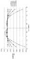
図14は、MOSアナログスイッチのオフ容量のバイアス電圧依存性の一例を示す図である。 FIG. 14 is a diagram illustrating an example of the bias voltage dependence of the off capacitance of the MOS analog switch.
図14を参照して、MOSアナログスイッチはオフ状態においても数pFのオフ容量を有しており、かつスイッチの両端に印加されるバイアス電圧に依存してオフ容量が変化する。 Referring to FIG. 14, the MOS analog switch has an off capacitance of several pF even in the off state, and the off capacitance changes depending on the bias voltage applied to both ends of the switch.
図15は、電荷電圧変換方式のセンサ装置において、図14に示すバイアス電圧依存性を有するMOSアナログスイッチを使用した場合の直線性誤差を示す図である。 FIG. 15 is a diagram showing a linearity error when the MOS analog switch having the bias voltage dependency shown in FIG. 14 is used in the charge-voltage conversion type sensor device.
図15を参照して、非特許文献2記載のセンサ装置等、電荷電圧変換方式のセンサ装置では、MOSアナログスイッチ等、帰還回路を構成するスイッチのオフ容量のバイアス電圧依存性に起因して、増幅器の出力電圧すなわちセンサ装置の出力特性が非線形になってしまう。特に、動脈内の圧力波形を測定する脈波測定装置においては、前述のように微小なセンサ素子を使用するため、良好なセンシング感度を確保するためには、帰還回路を構成するコンデンサの容量を小さくせざるを得ず、MOSアナログスイッチのオフ容量に起因するセンサ出力の誤差が大きくなる。 Referring to FIG. 15, in the sensor device of the charge voltage conversion method, such as the sensor device described in Non-Patent
それゆえに、本発明の目的は、出力特性が非線形になることを防ぎ、脈波検出の誤差を小さくすることが可能な脈波測定装置を提供することである。 SUMMARY OF THE INVENTION Therefore, an object of the present invention is to provide a pulse wave measuring device that can prevent an output characteristic from becoming nonlinear and reduce a pulse wave detection error.
上記課題を解決するために、この発明のある局面に係わる脈波測定装置は、生体の表面に押し当てることにより、動脈内の圧力波形を測定する脈波測定装置であって、動脈内の圧力に応じて静電容量が変化する圧力検出用コンデンサと、反転入力端子が圧力検出用コンデンサの一端に接続され、非反転入力端子が基準電圧に接続される演算増幅器と、一端が演算増幅器の反転入力端子に接続され、他端が演算増幅器の出力に接続される電荷転送用コンデンサと、一端が演算増幅器の反転入力端子に接続される第1のスイッチと、一端が第1のスイッチの他端に接続され、他端が演算増幅器の出力に接続される電圧設定部とを備え、電圧設定部は、第1のスイッチの他端および演算増幅器の出力を接続するか、あるいは第1のスイッチの他端および演算増幅器の出力を非接続として第1のスイッチの他端に所定電圧を印加する。 In order to solve the above-described problem, a pulse wave measuring device according to an aspect of the present invention is a pulse wave measuring device that measures a pressure waveform in an artery by pressing against a surface of a living body. A capacitor for pressure detection whose capacitance changes in accordance with the operational amplifier in which the inverting input terminal is connected to one end of the pressure detecting capacitor and the non-inverting input terminal is connected to the reference voltage, and one end of the operational amplifier is inverted. A charge transfer capacitor connected to the input terminal, the other end connected to the output of the operational amplifier, a first switch connected to the inverting input terminal of the operational amplifier, and one end connected to the other end of the first switch And the other end of the first switch is connected to the output of the operational amplifier, or the other end of the first switch is connected to the output of the operational amplifier. The other end The output of the fine operational amplifier to the other end of the first switch as a non-connected to apply a predetermined voltage.
好ましくは、電圧設定部は、一端が第1のスイッチの他端に接続され、他端が演算増幅器の出力に接続される第2のスイッチと、一端が第1のスイッチの他端に接続され、他端が所定電圧に接続される第3のスイッチとを含む。 Preferably, the voltage setting unit has one end connected to the other end of the first switch, the other end connected to the output of the operational amplifier, and one end connected to the other end of the first switch. And a third switch having the other end connected to a predetermined voltage.
好ましくは、電圧設定部は、一端が第1のスイッチの他端に接続され、他端が演算増幅器の出力に接続される第2のスイッチと、一端が第1のスイッチの他端に接続され、他端が所定電圧に接続される電圧設定用コンデンサとを含む。 Preferably, the voltage setting unit has one end connected to the other end of the first switch, the other end connected to the output of the operational amplifier, and one end connected to the other end of the first switch. And a voltage setting capacitor whose other end is connected to a predetermined voltage.
好ましくは、脈波測定装置は、さらに、圧力検出用コンデンサの他端に充電電圧を印加する充電部と、制御部とを備え、制御部は、充電部、第1のスイッチおよび電圧設定部を制御して、圧力検出用コンデンサの他端に充電電圧を印加し、第1のスイッチをオン状態とし、かつ第1のスイッチの他端および演算増幅器の出力を接続し、その後、第1のスイッチの他端および演算増幅器の出力を非接続とし、その後、第1のスイッチの他端に所定電圧を印加し、かつ充電電圧の印加を停止する。 Preferably, the pulse wave measurement device further includes a charging unit that applies a charging voltage to the other end of the pressure detection capacitor, and a control unit, and the control unit includes the charging unit, the first switch, and the voltage setting unit. Control to apply a charging voltage to the other end of the pressure detecting capacitor, turn on the first switch, and connect the other end of the first switch and the output of the operational amplifier; And the output of the operational amplifier are disconnected from each other, and then a predetermined voltage is applied to the other end of the first switch, and the application of the charging voltage is stopped.
好ましくは、脈波測定装置は、さらに、一端が圧力検出用コンデンサの一端に接続され、他端が演算増幅器の反転入力端子に接続される第4のスイッチを備える。 Preferably, the pulse wave measuring device further includes a fourth switch having one end connected to one end of the pressure detecting capacitor and the other end connected to the inverting input terminal of the operational amplifier.
より好ましくは、脈波測定装置は、さらに、圧力検出用コンデンサの他端に充電電圧を印加する充電部と、制御部とを備え、制御部は、充電部、第1のスイッチ、第4のスイッチおよび電圧設定部を制御して、圧力検出用コンデンサの他端に充電電圧を印加し、第1のスイッチをオン状態とし、第4のスイッチをオン状態とし、かつ第1のスイッチの他端および演算増幅器の出力を接続し、その後、第4のスイッチをオフ状態とし、その後、第1のスイッチの他端および演算増幅器の出力を非接続とし、その後、第1のスイッチの他端に所定電圧を印加し、かつ充電電圧の印加を停止し、その後、第4のスイッチをオン状態とする。 More preferably, the pulse wave measurement device further includes a charging unit that applies a charging voltage to the other end of the pressure detection capacitor, and a control unit, and the control unit includes the charging unit, the first switch, and the fourth switch. By controlling the switch and the voltage setting unit, the charging voltage is applied to the other end of the pressure detecting capacitor, the first switch is turned on, the fourth switch is turned on, and the other end of the first switch And the output of the operational amplifier are connected, and then the fourth switch is turned off, and then the other end of the first switch and the output of the operational amplifier are disconnected, and then the other end of the first switch is predetermined. The voltage is applied and the application of the charging voltage is stopped, and then the fourth switch is turned on.
好ましくは、所定電圧は基準電圧である。 Preferably, the predetermined voltage is a reference voltage.
本発明によれば、出力特性が非線形になることを防ぎ、脈波検出の誤差を小さくすることを防ぐことができる。 According to the present invention, it is possible to prevent the output characteristics from becoming non-linear and to reduce the error of pulse wave detection.
以下、本発明の実施の形態について図面を用いて説明する。なお、図中同一または相当部分には同一符号を付してその説明は繰り返さない。 Hereinafter, embodiments of the present invention will be described with reference to the drawings. In the drawings, the same or corresponding parts are denoted by the same reference numerals and description thereof will not be repeated.
<第1の実施の形態>
[脈波測定装置の構成および基本動作]
図1は、本発明の第1の実施の形態に係る脈波測定装置の外観図である。なお、図1は、センサアレイを手首に押圧した測定状態を示している。図2は、図1に示す測定状態における手首および脈波測定装置の模式断面図である。<First Embodiment>
[Configuration and basic operation of pulse wave measurement device]
FIG. 1 is an external view of a pulse wave measuring apparatus according to the first embodiment of the present invention. FIG. 1 shows a measurement state in which the sensor array is pressed against the wrist. 2 is a schematic cross-sectional view of the wrist and pulse wave measuring device in the measurement state shown in FIG.
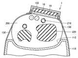
図1および図2を参照して、脈波測定装置100は、被験者の手首において動脈内の圧力波形を測定するためのものである。脈波測定装置100は、載置台110と、センサユニット1と、締付けベルト130とを備える。センサユニット1は、ケーシング122と、押圧カフ18と、センサアレイ19とを含む。 With reference to FIG. 1 and FIG. 2, the pulse
載置台110は、被験者の一方の腕200の手首および前腕を載置するための載置部112を含む。締付けベルト130は、載置台110に載置された腕200の手首部分を固定する。センサユニット1は、締付けベルト130に取付けられ、センサアレイ19を内蔵する。 The mounting table 110 includes a
図1を参照して、載置台110に手首が固定された状態においては、動脈210が腕200の延在方向と平行な方向に位置する。図2を参照して、センサユニット1のケーシング122内に内蔵された押圧カフ18が膨張することにより、センサアレイ19が下降し、手首の表面に向かってセンサアレイ19のセンサ面が押し当てられる。押圧カフ18は、後述する加圧ポンプ15および負圧ポンプ16により内圧が調整される。センサアレイ19は、センサ面に設けられた後述する下部電極31が動脈210の延在方向と略直交する方向に延在するように配置される。 Referring to FIG. 1, in a state where the wrist is fixed to mounting table 110,
押圧時においては、動脈210が橈骨220とセンサアレイ19のセンサ面とによって上下方向から挟み込まれれた状態となり、動脈210に平坦部が形成される。そして、動脈210に形成された平坦部の直上に少なくとも1個のセンサエレメント28が位置することになる。 At the time of pressing, the
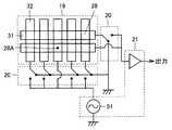
図3は、本発明の第1の実施の形態に係る脈波測定装置におけるセンサアレイ19、マルチプレクサ20およびC−V変換部21の構成を示す図である。図4は、センサアレイ19の外観斜視図である。 FIG. 3 is a diagram showing a configuration of the
図3を参照して、センサアレイ19は、マルチプレクサ20と、C−V変換部21と組み合わされて使用される。C−V変換部21は、充電部51を含む。 Referring to FIG. 3,
図4を参照して、センサアレイ19は、下部電極31と、上部電極32と、スペーサ部材30とを含む。下部電極31は、互いに並走するように行状に設けられた実質的に直線状に延びる複数の帯状銅箔電極からなる。上部電極32は、下部電極31と直交する方向に互いに並走するように列状に設けられた実質的に直線状に延びる複数の帯状銅箔電極からなる。下部電極31および上部電極32の間には、シリコンラバーからなるスペーサ部材30が配置される。 Referring to FIG. 4,
行列状に配置された下部電極31および上部電極32の交差部においては、スペーサ部材30によって所定の距離だけ離れて下部電極31と上部電極32とが対向配置される。これにより、下部電極31および上部電極32の交差部においてセンサエレメント28が形成される。すなわち、センサアレイ19は、行列状に配置された複数個のセンサエレメント28を含む。 At the intersection of the
センサエレメント28は、上部電極32または下部電極31に加わる圧力によって互いに接近する方向に歪むことにより、静電容量が変化する。 The
再び図3を参照して、下部電極31および上部電極32の一方の電極にマルチプレクサ20を介してC−V変換部21が接続される。マルチプレクサ20は、特定の下部電極31および上部電極32を選択する。このような構成により、行列状に配置された複数個のセンサエレメント28のうちのいずれか1個の静電容量をC−V変換部21の出力電圧として得ることが可能になる。たとえば、マルチプレクサ20が、上から2行目の下部電極31と左から3列目の上部電極32とを選択した場合には、センサエレメント28AがC−V変換部21に接続される。したがって、センサアレイ19の任意の位置における圧力波形を測定することが可能になる。なお、図3では上部電極32がマルチプレクサ20を介して充電部51に接続されているが、下部電極31および上部電極32の接続関係を逆にして下部電極31がマルチプレクサ20を介して充電部51に接続される構成であってもよい。 Referring to FIG. 3 again, the
図5は、本発明の第1の実施の形態に係る脈波測定装置の機能ブロック図である。
図5を参照して、脈波測定装置100は、センサユニット1と、表示ユニット3と、載置台110とを備える。表示ユニット3は、操作部24と、表示部25とを含む。センサユニット1は、押圧カフ18と、センサアレイ19とを含む。載置台110は、ROM(Read Only Memory)12と、RAM(Random Access Memory)13と、CPU(Central Processing Unit)(制御部)11と、駆動回路14と、加圧ポンプ15と、負圧ポンプ16と、切り替え弁17と、マルチプレクサ20と、C−V変換部21と、ローパスフィルタ22と、A/D変換部23とを含む。FIG. 5 is a functional block diagram of the pulse wave measurement device according to the first embodiment of the present invention.
Referring to FIG. 5, pulse
操作部24は、外部からの操作を検出し、検出結果を操作信号としてCPU11等に出力する。ユーザは、操作部24を操作して脈波測定に関する各種情報を脈波測定装置100に入力する。 The
表示部25は、動脈位置検出結果および脈波測定結果等の各種情報を外部に出力するためのLED(Light Emitting Diode)と、LCD(Liquid Crystal Display)とを含む。 The
ROM12およびRAM13は、たとえば、脈波測定装置100を制御するためのデータおよびプログラムを記憶する。 ROM12 and RAM13 memorize | store the data and program for controlling the pulse-
駆動回路14は、CPU11からの制御信号に基づいて加圧ポンプ15、負圧ポンプ16および切り替え弁17を駆動する。 The
CPU11は、ROM12にアクセスしてプログラムを読み出し、読み出したプログラムをRAM13上に展開して実行し、脈波測定装置100における各ブロックの制御および演算処理を行なう。また、CPU11は、操作部24から受けたユーザの操作信号に基づいて脈波測定装置100における各ブロックの制御処理を行なう。すなわち、CPU11は、操作部24から受けた操作信号に基づいて制御信号を各ブロックに出力する。また、CPU11は、脈波測定結果等を表示部25に表示する。 The
加圧ポンプ15は、押圧カフ18の内圧を加圧するためのポンプであり、また、負圧ポンプ16は、押圧カフ18の内圧を減圧するためのポンプである。切り替え弁17は、加圧ポンプ15および負圧ポンプ16のいずれかを選択的にエア管6に接続する。 The
押圧カフ18は、センサアレイ19を手首上に押圧させるために加圧調整される空気袋を含む。 The
センサアレイ19は、押圧カフ18の圧力によって被験者の手首等の測定部位に押圧される。センサアレイ19は、押圧された状態で、撓骨動脈を介して被験者の脈波すなわち動脈内の圧力波形を検出する。 The
マルチプレクサ20は、CPU11から受けた制御信号に基づいて、センサアレイ19における複数個のセンサエレメント28のうちのいずれか1個を選択する。C−V変換部21は、マルチプレクサ20が選択したセンサエレメント28の静電容量値を電圧に変換する、すなわち動脈内の圧力波形を表わす、動脈から生体表面に伝達される圧力振動波を電圧信号として出力する(以下、圧力信号とも称する)。 The
ローパスフィルタ22は、C−V変換部21から受けた圧力信号のうち、所定の周波数成分を減衰させる。 The low-
A/D変換部23は、ローパスフィルタ22を通過したアナログ信号である圧力信号をデジタル信号に変換してCPU11に出力する。 The A /
なお、載置台110が表示ユニット3を含む構成であってもよい。また、載置台110がCPU11、ROM12およびRAM13を備える構成としたが、これらを表示ユニット3が含む構成としてもよい。また、CPU11がPC(Personal Computer)と接続されて、各種制御を行なう構成であってもよい。 The mounting table 110 may include the
[脈波測定装置の動作]
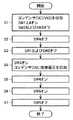
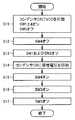
図6は、本発明の第1の実施の形態に係る脈波測定装置が脈波測定を行なう際の動作手順を定めたフローチャートである。図6のフローチャートに示される処理は、CPU11が、ROM22にアクセスしてプログラムを読み出し、読み出したプログラムをRAM23上に展開して実行することによって実現される。[Operation of pulse wave measuring device]
FIG. 6 is a flowchart defining an operation procedure when the pulse wave measuring apparatus according to the first embodiment of the present invention performs pulse wave measurement. The processing shown in the flowchart of FIG. 6 is realized by the
図6を参照して、まず、脈波測定装置100に電源が投入されると、CPU11は、駆動回路14に対して負圧ポンプ16を駆動するように指示する。駆動回路14は、CPU11からの指示に基づいて切り替え弁17を負圧ポンプ16側に切り替え、負圧ポンプ16を駆動する(S101)。駆動された負圧ポンプ16は、切り替え弁17を介して押圧カフ18の内圧が大気圧よりも十分に低くなるように減圧する。このような構成により、センサアレイ19が不用意に突出して誤動作および故障が生じることを回避できる。 Referring to FIG. 6, first, when power is turned on to pulse
CPU11は、センサアレイ19が測定部位に移動したことを検知すると(S102)、脈波測定を開始する。ここで、センサユニット1は、センサアレイ19の移動を検知するための図示しないマイクロスイッチ等を備え、CPU11は、マイクロスイッチの検出信号に基づいてセンサアレイ19の位置を認識する。なお、CPU11は、操作部24に含まれる測定開始スイッチ(図示せず)が押されたことを検知すると、脈波測定を開始する構成であってもよい。 When the
CPU11は、センサアレイ19が測定部位に移動すると(S102でYES)、駆動回路14に対し、加圧ポンプ15を駆動するように指示する。駆動回路14は、CPU11からの指示に基づいて切り替え弁17を加圧ポンプ15側に切り替え、加圧ポンプ15を駆動する(S103)。駆動された加圧ポンプ15は、切り替え弁17を介して押圧カフ18の内圧を加圧し、センサアレイ19を被験者の測定部位の表面に押圧する。 When the
センサアレイ19が測定部位に押圧されると、マルチプレクサ20は、CPU11の制御に基づいて、C−V変換部21に接続するセンサエレメント28を時分割で切り替える。C−V変換部21は、マルチプレクサ20が選択したセンサエレメント28の静電容量値を電圧に変換する。ローパスフィルタ22は、C−V変換部21から受けた圧力信号のうち、所定の周波数成分を減衰させる。A/D変換部23は、ローパスフィルタ22を通過した圧力信号をデジタル情報に変換し、CPU11に出力する。 When the
CPU11は、A/D変換部23から受けたデジタル情報に基づいてセンサエレメント28の位置と圧力信号との関係を表わすトノグラムを作成し、表示部25に表示する(S104)。 The
CPU11は、作成したトノグラムに基づいて、動脈上に位置するセンサエレメント28を検出して選択する(S105)。なお、センサエレメント28を検出する処理については、本願出願人がすでに出願して公開されている特開2004−222847号公報に記載の技術等を用いることができる。 The
また、CPU11は、A/D変換部23から受けたデジタル情報に基づいて、C−V変換部21から出力される圧力信号の直流成分を抽出する(S106)。圧力信号の直流成分は、所定期間の圧力信号の平均値、圧力信号のうちの所定周波数以下の成分すなわち脈波成分を除去した圧力信号、および脈波立上り点すなわち脈波成分が混入する直前の圧力信号レベル等で表わされる。 Further, the
より具体的には、圧力信号の出力変化を所定期間ごとのウィンドウ(区間)に分割し、各ウィンドウ内の平均を算出することで、直流成分を抽出することができる。あるいは、各ウィンドウ内の最大値と最小値との中間値を算出する等を行なっても、同様に直流成分を抽出することができる。なお、上述の所定期間は、被験者の脈拍に拠らない予め脈波測定装置100に設定されている期間であり、一般的な脈拍の間隔以上である1.5秒程度であることが好ましい。 More specifically, the direct current component can be extracted by dividing the output change of the pressure signal into windows (sections) for each predetermined period and calculating the average in each window. Alternatively, the DC component can be similarly extracted by calculating an intermediate value between the maximum value and the minimum value in each window. In addition, the above-mentioned predetermined period is a period set in advance in the pulse
次に、CPU11は、駆動回路14を制御して最適圧力調整を行なう、すなわち圧力信号の直流成分が安定するように押圧カフ18の内圧を調整する(S107)。 Next, the
次に、CPU11は、A/D変換部23から受けたデジタル情報が表わす、現在選択しているC−V変換部21からの圧力信号に基づいて、波形データを取得し、取得した波形データに基づいて脈波を測定する(S108)。 Next, the
そして、CPU11は、脈波測定の終了条件が成立した場合には(S109でYES)、駆動回路14を制御して負圧ポンプ16を駆動し、測定部位に対するセンサアレイ19の押圧状態を解除する(S110)。ここで、脈波測定の終了条件は、予め設定された所定時間(たとえば30秒)の経過であってもよいし、ユーザからの測定終了の指示および測定中断の指示等であってもよい。 When the pulse wave measurement end condition is satisfied (YES in S109), the
一方、CPU11は、所定条件が成立しない場合には(S109でNO)、波形データの転送処理を繰り返し行ない、脈波測定を継続する(S108)。 On the other hand, if the predetermined condition is not satisfied (NO in S109), the
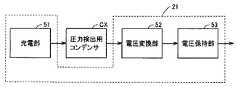
[C−V変換部およびセンサエレメントの構成および基本動作]
図7は、本発明の第1の実施の形態に係る脈波測定装置におけるC−V変換部21およびコンデンサCXの構成を示す機能ブロック図である。[Configuration and basic operation of CV conversion unit and sensor element]
FIG. 7 is a functional block diagram showing configurations of the
図7を参照して、C−V変換部21は、充電部51と、電圧変換部52と、電圧保持部53とを含む。コンデンサ(圧力検出用コンデンサ)CXは、センサエレメント28に対応する。なお、図7では説明を簡単にするためにマルチプレクサ20を図示せず、また、マルチプレクサ20が選択したコンデンサCXのみを示している。 Referring to FIG. 7,
コンデンサCXは、脈波測定装置100のセンサアレイ19が生体の表面に押し当てられた状態において、生体の動脈内の圧力に応じて静電容量が変化する。 Capacitor CX changes its capacitance according to the pressure in the artery of the living body when
充電部51は、コンデンサCXに充電電圧を印加して電荷を蓄える。電圧変換部52は、コンデンサCXに蓄えられた電荷に基づいてコンデンサCXの静電容量を表わす変換電圧を生成し、電圧保持部53に出力する。電圧保持部53は、電圧変換部52から受けた変換電圧を保持するとともにローパスフィルタ22へ出力する。 The charging
図8は、本発明の第1の実施の形態に係る脈波測定装置におけるC−V変換部21およびコンデンサCXの構成を示す回路図である。 FIG. 8 is a circuit diagram showing the configurations of the
図8を参照して、C−V変換部21は、センサエレメント28に対応するコンデンサ(圧力検出用コンデンサ)CXと組み合わせて使用される。C−V変換部21は、コンデンサCCと、電荷転送用コンデンサCFと、コンデンサCH1と、スイッチ(第1のスイッチ)SW1と、スイッチ(第4のスイッチ)SW4と、スイッチSW5と、演算増幅器G1およびG2と、充電部51と、電圧設定部54とを備える。充電部51は、スイッチSW51〜SW54と、電源V1およびV2とを含む。電圧設定部54は、スイッチ(第2のスイッチおよび第3のスイッチ)SW2およびSW3を含む。スイッチSW1〜SW5は、たとえばMOSアナログスイッチである。なお、図8では説明を簡単にするためにマルチプレクサ20を図示せず、また、マルチプレクサ20が選択したコンデンサCXのみを示している。 Referring to FIG. 8,
ここで、演算増幅器G1と、スイッチSW1と、コンデンサCFと、電圧設定部54とが、図7に示す電圧変換部52に対応する。また、スイッチSW5と、コンデンサCH1とが、図7に示す電圧保持部53に対応する。 Here, the operational amplifier G1, the switch SW1, the capacitor CF, and the
演算増幅器G1は、反転入力端子がコンデンサCXの一端およびコンデンサCCの一端に接続され、非反転入力端子が接地電圧(基準電圧)に接続される。コンデンサCFは、一端が演算増幅器G1の反転入力端子に接続され、他端が演算増幅器G1の出力に接続される。スイッチSW1は、一端が演算増幅器G1の反転入力端子に接続され、他端が電圧設定部54の一端に接続される。電圧設定部54は、他端が演算増幅器G1の出力に接続される。 The operational amplifier G1 has an inverting input terminal connected to one end of the capacitor CX and one end of the capacitor CC, and a non-inverting input terminal connected to the ground voltage (reference voltage). One end of the capacitor CF is connected to the inverting input terminal of the operational amplifier G1, and the other end is connected to the output of the operational amplifier G1. The switch SW1 has one end connected to the inverting input terminal of the operational amplifier G1 and the other end connected to one end of the
電圧設定部54において、スイッチSW2は、一端がスイッチSW1の他端に接続され、他端が演算増幅器G1の出力に接続される。スイッチSW3は、一端がスイッチSW1の他端に接続され、他端が接地電圧(基準電圧)に接続される。 In the
スイッチSW5は、一端が演算増幅器G1の出力に接続され、他端がコンデンサCH1の一端および演算増幅器G2の非反転入力端子に接続される。コンデンサCH1の他端が接地電圧に接続される。演算増幅器G2の反転入力端子が演算増幅器G2の出力に接続される。 The switch SW5 has one end connected to the output of the operational amplifier G1, and the other end connected to one end of the capacitor CH1 and the non-inverting input terminal of the operational amplifier G2. The other end of the capacitor CH1 is connected to the ground voltage. The inverting input terminal of the operational amplifier G2 is connected to the output of the operational amplifier G2.
充電部51において、スイッチSW51の一端が電源V1の正電極に接続され、他端がスイッチSW52の一端およびコンデンサCXの他端に接続される。スイッチSW54の一端が電源V2の負電極に接続され、他端がスイッチSW53の一端およびコンデンサCCの他端に接続される。スイッチSW52の他端と、スイッチSW53の他端と、電源V1の負電極と、電源V2の正電極とが接地電圧に接続される。また、電源V1およびV2の出力電圧値はVCCである。 In the charging
コンデンサCCは、カウンタ容量と呼ばれ、コンデンサCXの静電容量のオフセットを調整する目的で配置される。 The capacitor CC is called a counter capacitance, and is arranged for the purpose of adjusting the offset of the capacitance of the capacitor CX.
スイッチSW1〜SW5は、それぞれCPU11から受けた制御信号SC1〜SC5に基づいてオン状態およびオフ状態を切り替える。スイッチSW51〜SW54は、CPU11から受けた図示しない制御信号に基づいてオン状態およびオフ状態を切り替える。 Switches SW1 to SW5 switch between an on state and an off state based on control signals SC1 to SC5 received from
電圧設定部54は、スイッチSW1の他端および演算増幅器G1の出力を接続するか、あるいはスイッチSW1の他端および演算増幅器G1の出力を非接続としてスイッチSW1の他端に接地電圧を印加する。 The
[C−V変換部の動作]
図9は、本発明の第1の実施の形態に係る脈波測定装置が脈波測定を行なう際のC−V変換部21の動作を示すタイムチャートである。VPはコンデンサCXの他端に印加される電圧であり、VNはコンデンサCCの他端に印加される電圧であり、VG1は演算増幅器G1の出力電圧であり、VOUTは演算増幅器G2の出力電圧である。制御信号SC1〜SC5がハイレベルの場合はそれぞれ対応するスイッチSW1〜SW5がオン状態となり、ローレベルの場合はオフ状態となる。[Operation of CV conversion unit]
FIG. 9 is a time chart showing the operation of the
図10は、本発明の第1の実施の形態に係る脈波測定装置が脈波測定を行なう際のC−V変換部21の動作手順を定めたフローチャートである。図10のフローチャートに示される処理は、CPU11が、ROM22にアクセスしてプログラムを読み出し、読み出したプログラムをRAM23上に展開して実行することによって実現される。 FIG. 10 is a flowchart defining the operation procedure of the
図9および図10を参照して、まず、CPU11は、スイッチSW1、SW2およびSW4をオン状態とし、かつスイッチSW3およびSW5をオフ状態とする。また、CPU11は、スイッチSW52およびSW53をオフ状態とし、かつスイッチSW51およびSW54をオン状態とすることにより、コンデンサCXの他端に充電電圧VCCを印加し、かつコンデンサCCの他端に充電電圧−VCCすなわち充電電圧VCCと絶対値が等しくかつ印加方向が逆の電圧を印加する(ステップS1)。 Referring to FIGS. 9 and 10, first,
ここで、演算増幅器G1の非反転入力端子に印加されている電圧すなわち接地電圧が演算増幅器G1の出力から演算増幅器G1の反転入力端子に帰還される。したがって、コンデンサCXに充電電圧VCCに対応する電荷が蓄えられ、また、コンデンサCCに充電電圧−VCCに対応する電荷が蓄えられる。 Here, the voltage applied to the non-inverting input terminal of the operational amplifier G1, that is, the ground voltage is fed back from the output of the operational amplifier G1 to the inverting input terminal of the operational amplifier G1. Therefore, a charge corresponding to the charging voltage VCC is stored in the capacitor CX, and a charge corresponding to the charging voltage −VCC is stored in the capacitor CC.
次に、CPU11は、スイッチSW4をオフ状態とする(ステップS2)。
次に、CPU11は、スイッチSW1およびSW2をオフ状態とすることにより、スイッチSW1の他端および演算増幅器G1の出力を非接続とする(ステップS3)。Next, the
Next, the
次に、CPU11は、スイッチSW3をオン状態とすることにより、スイッチSW1の他端に接地電圧(基準電圧)を印加する。また、CPU11は、スイッチSW52およびSW53をオン状態とし、かつスイッチSW51およびSW54をオフ状態とすることにより、充電電圧VCCおよび−VCCの印加を停止し、コンデンサCXの他端およびコンデンサCCの他端に接地電圧(基準電圧)を印加する(ステップS4)。 Next, the
次に、CPU11は、スイッチSW4をオン状態とする。そうすると、コンデンサCXに蓄えられた電荷量およびコンデンサCCに蓄えられた電荷量の差に対応する電荷がコンデンサCFに移動する。そして、演算増幅器G1からは、コンデンサCFに蓄えられた電荷に対応する電圧が出力電圧G1として出力される(ステップS5)。より詳細には、コンデンサCXの静電容量をCXとし、コンデンサCCの静電容量をCCとし、充電電圧VCCの電圧値をVCCとすると、コンデンサCFに移動する電荷は、(CX−CC)×VCCで表わされる。コンデンサCFに移動した電荷は、コンデンサCFの静電容量をCFとすると、演算増幅器G1によって((CX−CC)/CF)×VCCで表わされる電圧に変換される。 Next, the
次に、CPU11は、スイッチSW5をオン状態とする。これにより、演算増幅器G1の出力電圧に基づいてコンデンサCH1が充電される(ステップS6)。 Next, the
次に、CPU11は、スイッチSW5をオフ状態とする。これにより、演算増幅器G2の非反転入力端子に入力される電圧が固定される。そして、演算増幅器G2からは、コンデンサCH1に蓄えられている電荷に対応する電圧すなわち生体の動脈内の圧力に対応する電圧が出力電圧VOUTとしてローパスフィルタ22に出力される(ステップS7)。 Next, the
CPU11は、ステップS1〜S7の処理を繰り返すことにより、C−V変換部21から出力される圧力信号を更新する。これにより、動脈内の圧力波形が測定される。 CPU11 updates the pressure signal output from the
ところで、非特許文献2記載のセンサ装置等、電荷電圧変換方式のセンサ装置では、MOSアナログスイッチ等、帰還回路を構成するスイッチのオフ容量のバイアス電圧依存性に起因して、増幅器の出力電圧すなわちセンサ装置の出力特性が非線形になってしまうという問題点があった。しかしながら、本発明の第1の実施の形態に係る脈波測定装置では、CPU11は、スイッチSW1およびSW2をオフ状態とすることにより、スイッチSW1の他端および演算増幅器G1の出力を非接続とする。そして、CPU11は、スイッチSW3をオン状態とすることにより、スイッチSW1の他端に所定電圧たとえば接地電圧を印加する。ここで、スイッチSW3をオン状態とするとき、演算増幅器G1の反転入力端子には接地電圧が演算増幅器G1の出力から帰還されており、スイッチSW1の一端には接地電圧が印加されている。このような構成により、電荷転送動作(ステップS5)の際にスイッチSW1の両端に印加されるバイアス電圧を一定値とすることができるため、センサの出力特性が非線形になることを防ぎ、脈波検出の誤差を小さくすることができる。 By the way, in the charge voltage conversion type sensor device such as the sensor device described in
また、本発明の第1の実施の形態に係る脈波測定装置では、CPU11は、スイッチSW1の他端に演算増幅器G1の非反転入力端子に印加されている電圧である接地電圧を印加する構成により、スイッチSW1の両端に同じ電圧を印加することでスイッチSW1のオフ容量をほぼ0とすることができ、センサの出力特性の誤差をさらに小さくすることができる。 In the pulse wave measurement device according to the first embodiment of the present invention, the
また、本発明の第1の実施の形態に係る脈波測定装置は、一端がコンデンサCXの一端に接続され、他端が演算増幅器G1の反転入力端子に接続されるスイッチSW4を備える。そして、CPU11は、コンデンサCXに充電電圧VCCに対応する電荷が蓄えられた後、スイッチSW4をオフ状態とする。そして、スイッチSW1の他端および演算増幅器G1の出力を非接続とし、かつ、スイッチSW1の他端に接地電圧を印加する。その後、CPU11は、スイッチSW4をオン状態として、コンデンサCXに蓄えられた電荷をコンデンサCFに移動する。このように、スイッチSW1の両端に印加されるバイアス電圧を一定値とし、かつオフ容量をほぼ0とすることで、コンデンサCXに蓄えられた電荷量およびコンデンサCCに蓄えられた電荷量の差に対応する電荷をコンデンサCFに移動する際にスイッチSW1のオフ容量にも電荷が移動することを防ぐことができ、電荷移動がコンデンサCFのみに限定されるため、センサ出力の直線性が良好となる。 The pulse wave measuring apparatus according to the first embodiment of the present invention includes a switch SW4 having one end connected to one end of the capacitor CX and the other end connected to the inverting input terminal of the operational amplifier G1. Then, after the electric charge corresponding to the charging voltage VCC is stored in the capacitor CX, the
また、本発明の第1の実施の形態に係る脈波測定装置では、スイッチSW3としてたとえばMOSアナログスイッチを使用する。このような構成では、C−V変換部21を集積回路で構成した場合に同じプロセスでスイッチSW3を構成することができ、C−V変換部の小型化を図ることができる。 In the pulse wave measuring device according to the first embodiment of the present invention, for example, a MOS analog switch is used as the switch SW3. In such a configuration, when the
また、本発明の第1の実施の形態に係る脈波測定装置では、充電電圧の印加を停止するとき、コンデンサCXの他端に基準電圧を印加する。より詳細には、CPU11は、コンデンサCXの他端への充電電圧VCCの印加を停止するとき、コンデンサCXの他端に演算増幅器G1の非反転入力端子に印加されている電圧である接地電圧を印加する。このような構成により、演算増幅器G1を直線性の良い範囲で動作させることができる。 Moreover, in the pulse wave measuring apparatus according to the first embodiment of the present invention, when the application of the charging voltage is stopped, the reference voltage is applied to the other end of the capacitor CX. More specifically, when the
次に、本発明の他の実施の形態について図面を用いて説明する。なお、図中同一または相当部分には同一符号を付してその説明は繰り返さない。 Next, another embodiment of the present invention will be described with reference to the drawings. In the drawings, the same or corresponding parts are denoted by the same reference numerals and description thereof will not be repeated.
<第2の実施の形態>
本実施の形態は、C−V変換部21の構成を変更した脈波測定装置に関する。<Second Embodiment>
The present embodiment relates to a pulse wave measurement device in which the configuration of the
[C−V変換部の構成]
図11は、本発明の第2の実施の形態に係る脈波測定装置におけるC−V変換部21およびコンデンサCXの構成を示す回路図である。[Configuration of CV Conversion Unit]
FIG. 11 is a circuit diagram showing configurations of the
図11を参照して、本発明の第2の実施の形態に係る電圧設定部54は、スイッチSW4の代わりにコンデンサ(電圧設定用コンデンサ)CSを含む。 Referring to FIG. 11,
コンデンサCSは、一端がスイッチSW1の他端およびスイッチSW2の一端に接続され、他端が所定電圧たとえば負電圧VEEに接続されている。 Capacitor CS has one end connected to the other end of switch SW1 and one end of switch SW2, and the other end connected to a predetermined voltage, for example, negative voltage VEE.
[C−V変換部の動作]
図12は、本発明の第2の実施の形態に係る脈波測定装置が脈波測定を行なう際のC−V変換部21の動作を示すタイムチャートである。VPはコンデンサCXの他端に印加される電圧であり、VNはコンデンサCCの他端に印加される電圧であり、VG1は演算増幅器G1の出力電圧であり、VOUTは演算増幅器G2の出力電圧である。制御信号SC1〜SC5がハイレベルの場合はそれぞれ対応するスイッチSW1〜SW5がオン状態となり、ローレベルの場合はオフ状態となる。[Operation of CV conversion unit]
FIG. 12 is a time chart showing the operation of the
図13は、本発明の第2の実施の形態に係る脈波測定装置が脈波測定を行なう際のC−V変換部21の動作手順を定めたフローチャートである。図13のフローチャートに示される処理は、CPU11が、ROM22にアクセスしてプログラムを読み出し、読み出したプログラムをRAM23上に展開して実行することによって実現される。 FIG. 13 is a flowchart that defines the operation procedure of the
図12および図13を参照して、まず、CPU11は、スイッチSW1、SW2およびSW4をオン状態とし、かつスイッチSW5をオフ状態とする。また、CPU11は、スイッチSW52およびSW53をオフ状態とし、かつスイッチSW51およびSW54をオン状態とすることにより、コンデンサCXの他端に充電電圧VCCを印加し、かつコンデンサCCの他端に充電電圧−VCCすなわち充電電圧VCCと絶対値が等しくかつ印加方向が逆の電圧を印加する(ステップS11)。 Referring to FIGS. 12 and 13, first,
ここで、演算増幅器G1の非反転入力端子に印加されている電圧すなわち接地電圧が演算増幅器G1の出力から演算増幅器G1の反転入力端子に帰還される。したがって、コンデンサCXに充電電圧VCCに対応する電荷が蓄えられ、また、コンデンサCCに充電電圧−VCCに対応する電荷が蓄えられる。 Here, the voltage applied to the non-inverting input terminal of the operational amplifier G1, that is, the ground voltage is fed back from the output of the operational amplifier G1 to the inverting input terminal of the operational amplifier G1. Therefore, a charge corresponding to the charging voltage VCC is stored in the capacitor CX, and a charge corresponding to the charging voltage −VCC is stored in the capacitor CC.
次に、CPU11は、スイッチSW4をオフ状態とする(ステップS12)。なお、ステップS11およびS12においては、スイッチSW1およびSW2がオン状態であるため、コンデンサCSにも電荷が蓄えられる。 Next, the
次に、CPU11は、スイッチSW1およびSW2をオフ状態とすることにより、スイッチSW1の他端および演算増幅器G1の出力を非接続とする(ステップS13)。ここで、コンデンサCSに蓄えられた電荷によってスイッチSW1の他端は接地電圧(基準電圧)に保たれる。 Next, the
次に、CPU11は、スイッチSW52およびSW53をオン状態とし、かつスイッチSW51およびSW54をオフ状態とすることにより、充電電圧VCCおよび−VCCの印加を停止し、コンデンサCXの他端およびコンデンサCCの他端に接地電圧(基準電圧)を印加する(ステップS14)。 Next, the
次に、CPU11は、スイッチSW4をオン状態とする。そうすると、コンデンサCXに蓄えられた電荷量およびコンデンサCCに蓄えられた電荷量の差に対応する電荷がコンデンサCFに移動する。そして、演算増幅器G1からは、コンデンサCFに蓄えられた電荷に対応する電圧が出力電圧G1として出力される(ステップS15)。より詳細には、コンデンサCXの静電容量をCXとし、コンデンサCCの静電容量をCCとし、充電電圧VCCの電圧値をVCCとすると、コンデンサCFに移動する電荷は、(CX−CC)×VCCで表わされる。コンデンサCFに移動した電荷は、コンデンサCFの静電容量をCFとすると、演算増幅器G1によって((CX−CC)/CF)×VCCで表わされる電圧に変換される。 Next, the
次に、CPU11は、スイッチSW5をオン状態とする。これにより、演算増幅器G1の出力電圧に基づいてコンデンサCH1が充電される(ステップS16)。 Next, the
次に、CPU11は、スイッチSW5をオフ状態とする。これにより、演算増幅器G2の非反転入力端子に入力される電圧が固定される。そして、演算増幅器G2からは、コンデンサCH1に蓄えられている電荷に対応する電圧すなわち生体の動脈内の圧力に対応する電圧が出力電圧VOUTとしてローパスフィルタ22に出力される(ステップS17)。 Next, the
CPU11は、ステップS11〜S17の処理を繰り返すことにより、C−V変換部21から出力される圧力信号を更新する。これにより、動脈内の圧力波形が測定される。 CPU11 updates the pressure signal output from the
その他の構成および動作は第1の実施の形態に係る脈波測定装置と同様であるため、ここでは詳細な説明を繰り返さない。 Since other configurations and operations are the same as those of the pulse wave measuring apparatus according to the first embodiment, detailed description thereof will not be repeated here.
したがって、本発明の第2の実施の形態に係る脈波測定装置では、第1の実施の形態に係る脈波測定装置と同様に、出力特性が非線形になることを防ぎ、脈波検出の誤差を小さくすることができる。 Therefore, in the pulse wave measurement device according to the second embodiment of the present invention, as in the pulse wave measurement device according to the first embodiment, the output characteristics are prevented from becoming non-linear, and the pulse wave detection error is prevented. Can be reduced.
今回開示された実施の形態はすべての点で例示であって制限的なものではないと考えられるべきである。本発明の範囲は上記した説明ではなくて特許請求の範囲によって示され、特許請求の範囲と均等の意味および範囲内でのすべての変更が含まれることが意図される。 The embodiment disclosed this time should be considered as illustrative in all points and not restrictive. The scope of the present invention is defined by the terms of the claims, rather than the description above, and is intended to include any modifications within the scope and meaning equivalent to the terms of the claims.
1 センサユニット、3 表示ユニット、11 CPU(制御部)、12 ROM、13 RAM、14 駆動回路、15 加圧ポンプ、16 負圧ポンプ、17 切り替え弁、18 押圧カフ、19 センサアレイ、20 マルチプレクサ、21 C−V変換部、22 ローパスフィルタ、23 A/D変換部、24 操作部、25 表示部、26 PCB、27 フレキシブル配線、28,28A センサエレメント、30 スペーサ部材、31 下部電極、32 上部電極、51 充電部、52 電圧変換部、53 電圧保持部、54 電圧設定部、55 差動増幅器、100 脈波測定装置、110 載置台、120 センサユニット、122 ケーシング、130 締付けベルト、200 腕、210 動脈、220 橈骨、CX コンデンサ(圧力検出用コンデンサ)、CC,CH1 コンデンサ、CF 電荷転送用コンデンサ、CS コンデンサ(電圧設定用コンデンサ)、SW1〜SW4 スイッチ(第1〜第4のスイッチ)、SW5,SW51〜SW54 スイッチ、G1〜G2 演算増幅器、V1,V2 電源。 DESCRIPTION OF
Claims (7)
Translated fromJapanese前記動脈内の圧力に応じて静電容量が変化する圧力検出用コンデンサと、
反転入力端子が前記圧力検出用コンデンサの一端に接続され、非反転入力端子が基準電圧に接続される演算増幅器と、
一端が前記演算増幅器の反転入力端子に接続され、他端が前記演算増幅器の出力に接続される電荷転送用コンデンサと、
一端が前記演算増幅器の反転入力端子に接続される第1のスイッチと、
一端が前記第1のスイッチの他端に接続され、他端が前記演算増幅器の出力に接続される電圧設定部とを備え、
前記電圧設定部は、前記第1のスイッチの他端および前記演算増幅器の出力を接続するか、あるいは前記第1のスイッチの他端および前記演算増幅器の出力を非接続として前記第1のスイッチの他端に所定電圧を印加する脈波測定装置。A pulse wave measuring device that measures a pressure waveform in an artery by pressing against the surface of a living body,
A pressure detecting capacitor whose capacitance changes according to the pressure in the artery;
An operational amplifier having an inverting input terminal connected to one end of the pressure sensing capacitor and a non-inverting input terminal connected to a reference voltage;
A charge transfer capacitor having one end connected to the inverting input terminal of the operational amplifier and the other end connected to the output of the operational amplifier;
A first switch having one end connected to the inverting input terminal of the operational amplifier;
A voltage setting unit having one end connected to the other end of the first switch and the other end connected to the output of the operational amplifier;
The voltage setting unit connects the other end of the first switch and the output of the operational amplifier, or disconnects the other end of the first switch and the output of the operational amplifier. A pulse wave measuring device that applies a predetermined voltage to the other end.
一端が前記第1のスイッチの他端に接続され、他端が前記演算増幅器の出力に接続される第2のスイッチと、
一端が前記第1のスイッチの他端に接続され、他端が前記所定電圧に接続される第3のスイッチとを含む請求項1記載の脈波測定装置。The voltage setting unit includes:
A second switch having one end connected to the other end of the first switch and the other end connected to the output of the operational amplifier;
The pulse wave measuring device according to claim 1, further comprising: a third switch having one end connected to the other end of the first switch and the other end connected to the predetermined voltage.
一端が前記第1のスイッチの他端に接続され、他端が前記演算増幅器の出力に接続される第2のスイッチと、
一端が前記第1のスイッチの他端に接続され、他端が前記所定電圧に接続される電圧設定用コンデンサとを含む請求項1記載の脈波測定装置。The voltage setting unit includes:
A second switch having one end connected to the other end of the first switch and the other end connected to the output of the operational amplifier;
The pulse wave measuring device according to claim 1, further comprising a voltage setting capacitor having one end connected to the other end of the first switch and the other end connected to the predetermined voltage.
前記圧力検出用コンデンサの他端に充電電圧を印加する充電部と、
制御部とを備え、
前記制御部は、前記充電部、前記第1のスイッチおよび前記電圧設定部を制御して、
前記圧力検出用コンデンサの他端に前記充電電圧を印加し、前記第1のスイッチをオン状態とし、かつ前記第1のスイッチの他端および前記演算増幅器の出力を接続し、その後、
前記第1のスイッチの他端および前記演算増幅器の出力を非接続とし、その後、
前記第1のスイッチの他端に前記所定電圧を印加し、かつ前記充電電圧の印加を停止する請求項1記載の脈波測定装置。The pulse wave measuring device further includes:
A charging unit for applying a charging voltage to the other end of the pressure detecting capacitor;
A control unit,
The control unit controls the charging unit, the first switch, and the voltage setting unit,
Applying the charging voltage to the other end of the pressure detection capacitor, turning on the first switch, and connecting the other end of the first switch and the output of the operational amplifier;
Disconnect the other end of the first switch and the output of the operational amplifier;
The pulse wave measuring device according to claim 1, wherein the predetermined voltage is applied to the other end of the first switch, and the application of the charging voltage is stopped.
一端が前記圧力検出用コンデンサの一端に接続され、他端が前記演算増幅器の反転入力端子に接続される第4のスイッチを備える請求項1記載の脈波測定装置。The pulse wave measuring device further includes:
The pulse wave measuring device according to claim 1, further comprising a fourth switch having one end connected to one end of the pressure detecting capacitor and the other end connected to an inverting input terminal of the operational amplifier.
前記圧力検出用コンデンサの他端に充電電圧を印加する充電部と、
制御部とを備え、
前記制御部は、前記充電部、前記第1のスイッチ、前記第4のスイッチおよび前記電圧設定部を制御して、
前記圧力検出用コンデンサの他端に前記充電電圧を印加し、前記第1のスイッチをオン状態とし、前記第4のスイッチをオン状態とし、かつ前記第1のスイッチの他端および前記演算増幅器の出力を接続し、その後、
前記第4のスイッチをオフ状態とし、その後、
前記第1のスイッチの他端および前記演算増幅器の出力を非接続とし、その後、
前記第1のスイッチの他端に前記所定電圧を印加し、かつ前記充電電圧の印加を停止し、その後、
前記第4のスイッチをオン状態とする請求項5記載の脈波測定装置。The pulse wave measuring device further includes:
A charging unit for applying a charging voltage to the other end of the pressure detecting capacitor;
A control unit,
The control unit controls the charging unit, the first switch, the fourth switch, and the voltage setting unit,
The charging voltage is applied to the other end of the pressure detecting capacitor, the first switch is turned on, the fourth switch is turned on, and the other end of the first switch and the operational amplifier Connect the output, then
Turn off the fourth switch, then
Disconnect the other end of the first switch and the output of the operational amplifier;
Applying the predetermined voltage to the other end of the first switch and stopping the application of the charging voltage;
The pulse wave measuring device according to claim 5, wherein the fourth switch is turned on.
Priority Applications (7)
| Application Number | Priority Date | Filing Date | Title |
|---|---|---|---|
| JP2006122206AJP4325638B2 (en) | 2006-04-26 | 2006-04-26 | Pulse wave measuring device |
| PCT/JP2007/057380WO2007125728A1 (en) | 2006-04-26 | 2007-04-02 | Pulse wave measuring device |
| CN2007800146425ACN101426421B (en) | 2006-04-26 | 2007-04-02 | Pulse wave measuring device |
| US12/293,233US20090209870A1 (en) | 2006-04-26 | 2007-04-02 | Pulse-wave measurement apparatus |
| EP07740816AEP2014227B1 (en) | 2006-04-26 | 2007-04-02 | Pulse wave measuring device |
| DE602007010759TDE602007010759D1 (en) | 2006-04-26 | 2007-04-02 | PULSE WAVE KNIFE |
| TW096114524ATW200803790A (en) | 2006-04-26 | 2007-04-25 | Pulse measuring device |
Applications Claiming Priority (1)
| Application Number | Priority Date | Filing Date | Title |
|---|---|---|---|
| JP2006122206AJP4325638B2 (en) | 2006-04-26 | 2006-04-26 | Pulse wave measuring device |
Publications (2)
| Publication Number | Publication Date |
|---|---|
| JP2007289501A JP2007289501A (en) | 2007-11-08 |
| JP4325638B2true JP4325638B2 (en) | 2009-09-02 |
Family
ID=38655263
Family Applications (1)
| Application Number | Title | Priority Date | Filing Date |
|---|---|---|---|
| JP2006122206AExpired - Fee RelatedJP4325638B2 (en) | 2006-04-26 | 2006-04-26 | Pulse wave measuring device |
Country Status (7)
| Country | Link |
|---|---|
| US (1) | US20090209870A1 (en) |
| EP (1) | EP2014227B1 (en) |
| JP (1) | JP4325638B2 (en) |
| CN (1) | CN101426421B (en) |
| DE (1) | DE602007010759D1 (en) |
| TW (1) | TW200803790A (en) |
| WO (1) | WO2007125728A1 (en) |
Cited By (1)
| Publication number | Priority date | Publication date | Assignee | Title |
|---|---|---|---|---|
| US9772222B2 (en) | 2014-12-08 | 2017-09-26 | Samsung Electronics Co., Ltd. | Retainer for photoelectric sensor and photoelectric pulse wave measuring apparatus including the same |
Families Citing this family (18)
| Publication number | Priority date | Publication date | Assignee | Title |
|---|---|---|---|---|
| JP4325638B2 (en)* | 2006-04-26 | 2009-09-02 | オムロンヘルスケア株式会社 | Pulse wave measuring device |
| FR2929055B1 (en)* | 2008-03-19 | 2010-05-28 | Commissariat Energie Atomique | SYSTEM FOR CONVERTING CHARGES IN VOLTAGE AND METHOD FOR CONTROLLING SUCH A SYSTEM |
| JP2011004327A (en) | 2009-06-22 | 2011-01-06 | Hamamatsu Photonics Kk | Integration circuit and photodetection device |
| JP5526761B2 (en)* | 2009-12-22 | 2014-06-18 | ソニー株式会社 | Sensor device and information processing device |
| WO2011125725A1 (en)* | 2010-03-31 | 2011-10-13 | 東海ゴム工業株式会社 | Capacitance-type sensor device and capacitance-type sensor capacitance measuring device |
| TW201249399A (en)* | 2011-06-09 | 2012-12-16 | Hon Hai Prec Ind Co Ltd | Electronic apparatus and detecting pulse method thereof |
| WO2013091909A1 (en) | 2011-12-23 | 2013-06-27 | Imec | Method and system for measuring capacitance difference between capacitive elements |
| US8836349B2 (en)* | 2012-08-15 | 2014-09-16 | Robert Bosch Gmbh | Capacitive sensor |
| KR101344405B1 (en) | 2012-11-13 | 2013-12-26 | 김시원 | Blood glucose meter with compensation bias circuit and blood glucose measurement method using same |
| KR101455815B1 (en)* | 2013-04-24 | 2014-11-12 | 주식회사 네오애플 | Pressure Sensor |
| WO2014195578A1 (en)* | 2013-06-03 | 2014-12-11 | Medieta Oy | Blood pressure measurement device |
| JP6240581B2 (en) | 2014-09-24 | 2017-11-29 | 株式会社アドバンテスト | Pulse wave sensor unit |
| CN104579183B (en)* | 2015-01-07 | 2017-11-17 | 复旦大学 | A kind of acquiring biological electric signals AFE(analog front end) using electric capacity passive amplifier as input stage |
| WO2016152714A1 (en)* | 2015-03-20 | 2016-09-29 | 住友理工株式会社 | Capacitive pulse wave measuring device |
| CN106017747A (en)* | 2015-03-25 | 2016-10-12 | 松下知识产权经营株式会社 | Pressure sensor |
| CN104990649B (en)* | 2015-07-29 | 2017-11-17 | 重庆交通大学 | A kind of simple steel strand prestress measurement apparatus and method |
| US10353511B2 (en) | 2016-08-19 | 2019-07-16 | Qualcomm Incorporated | Capacitance-to-voltage modulation circuit |
| US10874307B2 (en)* | 2017-01-24 | 2020-12-29 | Verily Life Sciences Llc | Digital artery blood pressure monitor |
Family Cites Families (8)
| Publication number | Priority date | Publication date | Assignee | Title |
|---|---|---|---|---|
| DE4042335A1 (en)* | 1990-02-12 | 1991-08-14 | Fraunhofer Ges Forschung | PRESSURE SENSOR ARRANGEMENT WITH A PRESSURE SENSOR, A REFERENCE ELEMENT AND A MEASURING CIRCUIT |
| JP2972552B2 (en)* | 1995-05-26 | 1999-11-08 | 日本電気株式会社 | Detection circuit and detection method for capacitive sensor |
| JP3265942B2 (en)* | 1995-09-01 | 2002-03-18 | 株式会社村田製作所 | Micro capacitance detection circuit |
| US5873898A (en)* | 1997-04-29 | 1999-02-23 | Medtronic, Inc. | Microprocessor capture detection circuit and method |
| JP3838201B2 (en) | 2003-01-21 | 2006-10-25 | オムロンヘルスケア株式会社 | Pulse wave detector |
| CN1631319A (en)* | 2003-12-23 | 2005-06-29 | 罗志昌 | Blood flow parameter non-invasive detecting method based on finger tip volume pulsation blood flow wave |
| JP2006020823A (en)* | 2004-07-08 | 2006-01-26 | Omron Healthcare Co Ltd | Array type capacitive pressure pulse wave sensor and pulse wave measuring apparatus equipped with the same |
| JP4325638B2 (en)* | 2006-04-26 | 2009-09-02 | オムロンヘルスケア株式会社 | Pulse wave measuring device |
- 2006
- 2006-04-26JPJP2006122206Apatent/JP4325638B2/ennot_activeExpired - Fee Related
- 2007
- 2007-04-02DEDE602007010759Tpatent/DE602007010759D1/enactiveActive
- 2007-04-02CNCN2007800146425Apatent/CN101426421B/ennot_activeExpired - Fee Related
- 2007-04-02USUS12/293,233patent/US20090209870A1/ennot_activeAbandoned
- 2007-04-02WOPCT/JP2007/057380patent/WO2007125728A1/enactiveApplication Filing
- 2007-04-02EPEP07740816Apatent/EP2014227B1/ennot_activeNot-in-force
- 2007-04-25TWTW096114524Apatent/TW200803790A/enunknown
Cited By (1)
| Publication number | Priority date | Publication date | Assignee | Title |
|---|---|---|---|---|
| US9772222B2 (en) | 2014-12-08 | 2017-09-26 | Samsung Electronics Co., Ltd. | Retainer for photoelectric sensor and photoelectric pulse wave measuring apparatus including the same |
Also Published As
| Publication number | Publication date |
|---|---|
| CN101426421A (en) | 2009-05-06 |
| JP2007289501A (en) | 2007-11-08 |
| CN101426421B (en) | 2011-01-12 |
| DE602007010759D1 (en) | 2011-01-05 |
| EP2014227B1 (en) | 2010-11-24 |
| WO2007125728A1 (en) | 2007-11-08 |
| US20090209870A1 (en) | 2009-08-20 |
| EP2014227A1 (en) | 2009-01-14 |
| EP2014227A4 (en) | 2009-07-22 |
| TW200803790A (en) | 2008-01-16 |
Similar Documents
| Publication | Publication Date | Title |
|---|---|---|
| JP4325638B2 (en) | Pulse wave measuring device | |
| CN100542480C (en) | Blood pressure measuring device and blood pressure measuring method | |
| CA3048964A1 (en) | Blood pressure measurement system using force resistive sensor array | |
| JP6991022B2 (en) | Display control unit and program | |
| JP5561674B2 (en) | Blood pressure measurement system | |
| KR102308547B1 (en) | Portable blood pressure measuring device | |
| CN111542261A (en) | Measuring device and program | |
| JP4363411B2 (en) | Pulse wave measuring device | |
| FI106528B (en) | The measuring arrangement | |
| US20070139385A1 (en) | Signal processing system | |
| Kiran Kolluri et al. | Wearable micro‐electro‐mechanical systems pressure sensors in health care: Advancements and trends—A review | |
| WO2008007549A1 (en) | Pulse wave output device simultaneously outputting pulse waveform and information on pulse wave | |
| CN111033203B (en) | Pressure measuring device and pressure measuring method | |
| JP3821099B2 (en) | Pulse wave measuring device | |
| JP5780505B1 (en) | Pulse wave and pressure detection application device, and blood vessel pulse wave measurement system | |
| Huang et al. | A tactile sensing array integrated with tension sensor for continuously monitoring blood pulse waves | |
| EP1897489A1 (en) | Pulse wave measuring instrument manufacturable at suppressed cost | |
| Ziaie et al. | An implantable pressure sensor cuff for tonometric blood pressure measurement | |
| KR20090030122A (en) | Complex biosignal sensor | |
| US20200221962A1 (en) | Measurement device and measurement method | |
| JP6970605B2 (en) | Blood pressure estimator | |
| JP2017047093A (en) | Pressure gauge, pressure measurement device, and sphygmomanometer | |
| KR200361681Y1 (en) | Sphygmomanometer with three-dimensional positioning function | |
| US20250321148A1 (en) | Design architecture for piezoresistive pressure sensor drivers and power management | |
| JP2001296311A (en) | 3-axis acceleration sensor |
Legal Events
| Date | Code | Title | Description |
|---|---|---|---|
| A621 | Written request for application examination | Free format text:JAPANESE INTERMEDIATE CODE: A621 Effective date:20090406 | |
| TRDD | Decision of grant or rejection written | ||
| A01 | Written decision to grant a patent or to grant a registration (utility model) | Free format text:JAPANESE INTERMEDIATE CODE: A01 Effective date:20090519 | |
| A01 | Written decision to grant a patent or to grant a registration (utility model) | Free format text:JAPANESE INTERMEDIATE CODE: A01 | |
| A61 | First payment of annual fees (during grant procedure) | Free format text:JAPANESE INTERMEDIATE CODE: A61 Effective date:20090601 | |
| FPAY | Renewal fee payment (event date is renewal date of database) | Free format text:PAYMENT UNTIL: 20120619 Year of fee payment:3 | |
| R150 | Certificate of patent or registration of utility model | Free format text:JAPANESE INTERMEDIATE CODE: R150 | |
| LAPS | Cancellation because of no payment of annual fees |