JP4325630B2 - 3D integration device - Google Patents
3D integration deviceDownload PDFInfo
- Publication number
- JP4325630B2 JP4325630B2JP2006069545AJP2006069545AJP4325630B2JP 4325630 B2JP4325630 B2JP 4325630B2JP 2006069545 AJP2006069545 AJP 2006069545AJP 2006069545 AJP2006069545 AJP 2006069545AJP 4325630 B2JP4325630 B2JP 4325630B2
- Authority
- JP
- Japan
- Prior art keywords
- integrated circuit
- opening
- circuit board
- openings
- microstrip line
- Prior art date
- Legal status (The legal status is an assumption and is not a legal conclusion. Google has not performed a legal analysis and makes no representation as to the accuracy of the status listed.)
- Expired - Fee Related
Links
Images


Classifications
- H—ELECTRICITY
- H01—ELECTRIC ELEMENTS
- H01L—SEMICONDUCTOR DEVICES NOT COVERED BY CLASS H10
- H01L25/00—Assemblies consisting of a plurality of semiconductor or other solid state devices
- H01L25/03—Assemblies consisting of a plurality of semiconductor or other solid state devices all the devices being of a type provided for in a single subclass of subclasses H10B, H10D, H10F, H10H, H10K or H10N, e.g. assemblies of rectifier diodes
- H01L25/04—Assemblies consisting of a plurality of semiconductor or other solid state devices all the devices being of a type provided for in a single subclass of subclasses H10B, H10D, H10F, H10H, H10K or H10N, e.g. assemblies of rectifier diodes the devices not having separate containers
- H01L25/065—Assemblies consisting of a plurality of semiconductor or other solid state devices all the devices being of a type provided for in a single subclass of subclasses H10B, H10D, H10F, H10H, H10K or H10N, e.g. assemblies of rectifier diodes the devices not having separate containers the devices being of a type provided for in group H10D89/00
- H01L25/0657—Stacked arrangements of devices
- H—ELECTRICITY
- H01—ELECTRIC ELEMENTS
- H01P—WAVEGUIDES; RESONATORS, LINES, OR OTHER DEVICES OF THE WAVEGUIDE TYPE
- H01P1/00—Auxiliary devices
- H01P1/10—Auxiliary devices for switching or interrupting
- H01P1/15—Auxiliary devices for switching or interrupting by semiconductor devices
- H—ELECTRICITY
- H01—ELECTRIC ELEMENTS
- H01L—SEMICONDUCTOR DEVICES NOT COVERED BY CLASS H10
- H01L23/00—Details of semiconductor or other solid state devices
- H01L23/48—Arrangements for conducting electric current to or from the solid state body in operation, e.g. leads, terminal arrangements ; Selection of materials therefor
- H—ELECTRICITY
- H01—ELECTRIC ELEMENTS
- H01P—WAVEGUIDES; RESONATORS, LINES, OR OTHER DEVICES OF THE WAVEGUIDE TYPE
- H01P1/00—Auxiliary devices
- H01P1/20—Frequency-selective devices, e.g. filters
- H01P1/2005—Electromagnetic photonic bandgaps [EPB], or photonic bandgaps [PBG]
- H—ELECTRICITY
- H01—ELECTRIC ELEMENTS
- H01P—WAVEGUIDES; RESONATORS, LINES, OR OTHER DEVICES OF THE WAVEGUIDE TYPE
- H01P3/00—Waveguides; Transmission lines of the waveguide type
- H01P3/02—Waveguides; Transmission lines of the waveguide type with two longitudinal conductors
- H01P3/08—Microstrips; Strip lines
- H—ELECTRICITY
- H01—ELECTRIC ELEMENTS
- H01L—SEMICONDUCTOR DEVICES NOT COVERED BY CLASS H10
- H01L2225/00—Details relating to assemblies covered by the group H01L25/00 but not provided for in its subgroups
- H01L2225/03—All the devices being of a type provided for in the same main group of the same subclass of class H10, e.g. assemblies of rectifier diodes
- H01L2225/04—All the devices being of a type provided for in the same main group of the same subclass of class H10, e.g. assemblies of rectifier diodes the devices not having separate containers
- H01L2225/065—All the devices being of a type provided for in the same main group of the same subclass of class H10
- H01L2225/06503—Stacked arrangements of devices
- H01L2225/06527—Special adaptation of electrical connections, e.g. rewiring, engineering changes, pressure contacts, layout
- H—ELECTRICITY
- H01—ELECTRIC ELEMENTS
- H01L—SEMICONDUCTOR DEVICES NOT COVERED BY CLASS H10
- H01L2225/00—Details relating to assemblies covered by the group H01L25/00 but not provided for in its subgroups
- H01L2225/03—All the devices being of a type provided for in the same main group of the same subclass of class H10, e.g. assemblies of rectifier diodes
- H01L2225/04—All the devices being of a type provided for in the same main group of the same subclass of class H10, e.g. assemblies of rectifier diodes the devices not having separate containers
- H01L2225/065—All the devices being of a type provided for in the same main group of the same subclass of class H10
- H01L2225/06503—Stacked arrangements of devices
- H01L2225/06541—Conductive via connections through the device, e.g. vertical interconnects, through silicon via [TSV]
- H—ELECTRICITY
- H01—ELECTRIC ELEMENTS
- H01L—SEMICONDUCTOR DEVICES NOT COVERED BY CLASS H10
- H01L2225/00—Details relating to assemblies covered by the group H01L25/00 but not provided for in its subgroups
- H01L2225/03—All the devices being of a type provided for in the same main group of the same subclass of class H10, e.g. assemblies of rectifier diodes
- H01L2225/04—All the devices being of a type provided for in the same main group of the same subclass of class H10, e.g. assemblies of rectifier diodes the devices not having separate containers
- H01L2225/065—All the devices being of a type provided for in the same main group of the same subclass of class H10
- H01L2225/06503—Stacked arrangements of devices
- H01L2225/06555—Geometry of the stack, e.g. form of the devices, geometry to facilitate stacking
- H—ELECTRICITY
- H01—ELECTRIC ELEMENTS
- H01L—SEMICONDUCTOR DEVICES NOT COVERED BY CLASS H10
- H01L2924/00—Indexing scheme for arrangements or methods for connecting or disconnecting semiconductor or solid-state bodies as covered by H01L24/00
- H01L2924/0001—Technical content checked by a classifier
- H01L2924/0002—Not covered by any one of groups H01L24/00, H01L24/00 and H01L2224/00
Landscapes
- Engineering & Computer Science (AREA)
- Microelectronics & Electronic Packaging (AREA)
- Power Engineering (AREA)
- Physics & Mathematics (AREA)
- Computer Hardware Design (AREA)
- General Physics & Mathematics (AREA)
- Condensed Matter Physics & Semiconductors (AREA)
- Electromagnetism (AREA)
- Optics & Photonics (AREA)
- Semiconductor Integrated Circuits (AREA)
- Structure Of Printed Boards (AREA)
- Near-Field Transmission Systems (AREA)
- Production Of Multi-Layered Print Wiring Board (AREA)
Description
Translated fromJapanese本発明は、複数の集積回路基板を積層してなる3次元集積化装置に関し、情報通信機器、ゲーム機器、コンピュータ機器などのシステム、特に、メモリーCPU機能、撮像機能素子及び信号処理装置機能、通信機能などを集約したシステムに用いて好適なもの3次元集積化装置に関するものである。 The present invention relates to a three-dimensional integration device formed by stacking a plurality of integrated circuit boards, and relates to systems such as information communication equipment, game equipment, and computer equipment, in particular, memory CPU functions, imaging function elements, signal processing equipment functions, and communications. The present invention relates to a three-dimensional integration apparatus suitable for use in a system in which functions and the like are integrated.
近年、LSIの高集積化の発展、動作周波数の加速により、LSIのI/Oの本数増加による、物理的信号線取り出しの限界の問題、信号品質(波形劣化)劣化の問題、信号部のI/O部の消費電力の増大の問題などが深刻化しつつある。 In recent years, due to the development of higher integration of LSIs and the acceleration of operating frequency, the problem of the limit of physical signal line extraction, the problem of signal quality (waveform deterioration) degradation, the I The problem of an increase in power consumption in the / O section is becoming serious.
このうち、電波を用いる手法では、
(1)アンテナをチップ上に設ける手法(例えば、非特許文献1参照)、
(2)インダクターの電磁結合を用いる手法(例えば、非特許文献2参照)、
(3)対抗したパッドで構成されたキャパシター結合を用いる方法(例えば、非特許文献3参照)、
などが検討されている。Of these, in the method using radio waves,
(1) A method of providing an antenna on a chip (for example, see Non-Patent Document 1),
(2) Method using electromagnetic coupling of inductor (for example, see Non-Patent Document 2),
(3) A method using capacitor coupling composed of opposed pads (for example, see Non-Patent Document 3),
Etc. are being considered.
しかしながら、上述の如き非特許文献1のようにアンテナをチップ上に設ける手法では、1つのLSIから発せられたアンテナからの出力が、LSI上の配線に電流を誘起してしまうという根本的な問題があり、又、非特許文献3の方法では、2−LSIの対応した結合には良いが、3つ以上のLSIの積層には拡張を確保するのが難しい、あるいは、用いるキャパシターサイズによっては消費電力が大きいなどの問題があった。2のケースにおいては、互いに上下、あるいは、左右に隣接したインダクター間の干渉が問題であった。 However, in the method of providing an antenna on a chip as in
又、このような構成の3次元LSIを搭載した場合、ボード上に搭載された他のLSIや、ボード上の配線、或いは搭載した機器の外部への不要輻射の問題がある。 In addition, when a three-dimensional LSI having such a configuration is mounted, there is a problem of unnecessary radiation to the outside of another LSI mounted on the board, wiring on the board, or mounted equipment.
そこで、本発明の目的は、上述の如き従来の問題点に鑑み、多ピン化、狭ピッチ化されるLSI間の接続の数々の問題を解決するにある。 Accordingly, an object of the present invention is to solve a number of problems related to the connection between LSIs having a large number of pins and a narrow pitch in view of the conventional problems as described above.
また、本発明の目的は、従来、無線接続を行う場合の最も大きな課題であった、LSI上や、無線チャンネル間の干渉、ボード上の他のLSIや配線への干渉などの問題を解決することにある。 In addition, the object of the present invention is to solve problems such as interference on LSIs and between wireless channels, interference on other LSIs and wiring on the board, which has been the biggest problem in the past when performing wireless connection. There is.
本発明の更に他の目的、本発明によって得られる具体的な利点は、以下に説明される実施の形態の説明から一層明らかにされる。 Other objects of the present invention and specific advantages obtained by the present invention will become more apparent from the description of embodiments described below.
本発明に係る3次元集積化装置は、それぞれ1つ以上のグランドプレーンを有し、当該グランドプレーン上の所望の場所に1つ以上の開口部が設けられ、この開口部には上記グランドプレーンと対をなして形成されたマイクロストリップラインの端部が位置され、上記マイクロストリップラインに接続され上記開口部の周囲長λに略相当する周波数にて信号の送信及び/又は受信を行う送信部及び又は受信部が設けられた少なくとも2枚の集積回路基板を積層してなり、各集積回路基板の各開口部は各グランドプレーンと垂直な方向において他の集積回路基板の開口部の少なくとも1つと重なっており、上記各開口部には、それぞれ送信部が接続されたマイクロストリップラインと受信部が接続されたマイクロストリップラインの各一端が形成されており、上記各集積回路基板の1つが信号の送信側として機能するとき他の集積回路基板が受信側として機能し、上記各開口部の周囲長λ(媒質の比誘電率、比透磁率がそれぞれε、μの時λe=λ/√ε・μ)で共振する性質を持ち、上記各開口部の周囲長λに略相当するマイクロ波帯以上の周波数にて、上記各開口部を介して各集積回路基板間で信号を非接触で伝送することを特徴とする。Each of the three-dimensional integration devices according to the present invention has one or more ground planes, and one or more openings are provided at desired locations on the ground plane. A transmitting section for transmitting and / or receiving a signal at a frequency substantially equal to a peripheral length λ of the opening connected to the microstrip line, the ends of the microstrip lines formed in pairs; Alternatively,at least two integrated circuit boards provided with a receiver are stacked, and each opening of each integrated circuit board overlaps at least one of the openings of another integrated circuit board in a direction perpendicular to each ground plane. in which,in each opening, each end of the microstrip line receiver is connected to each transmission unit is connected to microstrip lines form When one of the integrated circuit boards functions as a signal transmission side, the other integrated circuit board functions as a reception side, and the peripheral length λ of each opening (relative permittivity and relative permeability of the medium) Has a property of resonating at λe = λ / √ε · μ) when ε and μ, respectively, and passes through the openingsat frequencies above the microwave band substantially corresponding to the peripheral length λ of the openings. Thus, signals are transmitted in a non-contact manner between the integrated circuit boards.
また、本発明に係る3次元集積化装置において、上記各集積回路基板のうちの少なくとも1つの集積回路基板には、通信波長と同等の周期構造を有するパターンが形成され、上記周期構造は、シリコン基板の底部に形成され、その導電部のパターンが上記シリコン基板自体のキャリア濃度変化によって作製されている。In the three-dimensional integrated device according to the present invention,a pattern having a periodic structure equivalent to a communication wavelength is formed on at least one of the integrated circuit substrates, and the periodic structure is made of silicon. A conductive part pattern is formed on the bottom of the substrate by changing the carrier concentration of the silicon substrate itself.
さらに、本発明に係る3次元集積化装置において、上記各集積回路基板は、少なくとも1つ以上の電源ならびにグランド配線用の貫通ビアを有するシリコン基板からなり、上記貫通ビアに電気的に接続されたバンプを介して積層されている。 Furthermore, in the three-dimensional integrated device according to the present invention, each of the integrated circuit substrates is composed of a silicon substrate having at least one power supply and a through via for ground wiring, and is electrically connected to the through via. They are stacked via bumps.
本発明によれば、簡便な回路で積層されたLSIのチップ間信号伝送を金属的な接合なしで行うことが可能となり、多ピン化、狭ピッチ化されるLSI間の接続の数々の問題を解決することできる。 According to the present invention, it is possible to transmit signals between chips of LSIs stacked with a simple circuit without metallic bonding, and there are a number of problems in connection between LSIs that are multi-pin and narrow pitch. Can be solved.
例えば、その接続コストが高価になる一方で、信頼性としては低下する一方のチップ間積層時の信号I/Oの信頼性を大きく高めることできる。 For example, the reliability of signal I / O at the time of stacking between chips can be greatly increased while the connection cost becomes high and the reliability decreases.
又、LSIの動作速度が高速化することで、I/O部のSignal Integrityの問題などへの配慮が必要となってきているが、無線化を実現する事で実装設計的な工数の大幅削減が可能となる。 In addition, due to the increased operating speed of LSIs, consideration for issues such as signal integrity in the I / O section has become necessary. Is possible.
以上のワイヤレス伝送による3次元化は、バンプ形成や、スルーホール形成といった高価なプロセスを必要とせず、非常にローコストに形成が可能なばかりか、3次元化によって、各LSIチップ間の信号ライン距離が激減される事で、配線負荷が低減し、I/Oの低消費電力化が可能である他、信号伝送歪の観点からも非常有利となる。 The above three-dimensional wireless transmission does not require an expensive process such as bump formation or through-hole formation, and can be formed at a very low cost. As a result of the drastic reduction, the wiring load is reduced, the power consumption of I / O can be reduced, and it is very advantageous from the viewpoint of signal transmission distortion.
また、本発明によれば、従来、無線接続を行う場合の最も大きな課題であった、LSI上や、無線チャンネル間の干渉、ボード上の他のLSIや配線への干渉などの問題が解決される。 In addition, according to the present invention, problems such as interference on LSIs and between wireless channels, interference on other LSIs and wiring on the board, which were the biggest problems in the past when performing wireless connection, are solved. The
以下、本発明の実施の形態について、図面を参照して詳細に説明する。なお、本発明は以下の例に限定されるものではなく、本発明の要旨を逸脱しない範囲で、任意に変更可能であることは言うまでもない。 Hereinafter, embodiments of the present invention will be described in detail with reference to the drawings. Needless to say, the present invention is not limited to the following examples, and can be arbitrarily changed without departing from the gist of the present invention.
本発明は、例えば図1に示すような構成の3次元集積化装置10に適用される。 The present invention is applied to, for example, a three-
図1に示す3次元集積化装置10は、それぞれ1つグランドプレーン11A,11Bを有し、当該グランドプレーン11A,11B上の所望の場所に1つ開口部12A,12Bが設けられ、この開口部12A,12Bには上記グランドプレーン11A,11Bと対をなして形成されたマイクロストリップライン13A,13Bの開放端部が位置され、上記マイクロストリップライン13A,13Bにスイッチ14A,14Bを介して選択的に接続され上記開口部12A,12Bの周囲長λに略相当する周波数にて信号の送信及び受信を行う送信部15A,15B及び受信部16A,16Bが設けられたそれぞれシリコン基板からなる2枚の集積回路基板17A,17Bを積層してなる。上記各集積回路基板17A,17Bの各開口部12A,12Bは、各グランドプレーン11A,11Bと垂直な方向において互いに重なる位置に設けられている。 The three-
このような構成の3次元集積化装置10では、上記マイクロストリップライン13A,13Bの開放端部が位置された各開口部12A,12Bが所謂スロットアンテナとして機能し、上記送信部15A,15B及び受信部16A,16Bにより、上記各開口部12A,12Bの周囲長λに略相当する周波数にて、上記各開口部12A,12Bを介して各集積回路基板間17A,17Bで信号を非接触で伝送することができる。 In the three-
すなわち、上記3次元集積化装置10において、上記マイクロストリップライン13A,13Bと、その開放端部が位置された各開口部12A,12Bは、上記開口部12A,12Bの周囲長λに略相当する周波数にて信号の送信及び受信を行う通信用素子として機能する。 That is, in the three-
この通信用素子は、グランドプレーン11A,11Bの開口部12A,12Bの周囲長λ(媒質の比誘電率、比透磁率がそれぞれε、μの時λe=λ/√ε・μ)で共振する性質を持ち、特にマイクロ波(概略>5GHz)波帯以上で有効な通信素子となる。 This communication element resonates at the peripheral length λ of the
開口部12A,12Bの形状は、細長いスリット状でも、長方形でも、不定形でも何でも良いが、構成される誘電材料の実効比誘電率、比透磁率を、それぞれ4、1とし、正方形を仮定すると正方形の1辺の長さは伝送周波数10GHzのとき約3.75mm、30GHzのとき1.25mm、60GHzの時0.625mmとなりLSI上に複数個の通信用素子を並べることができる。
LSI上に複数個の通信用素子を並べることにより、例えば、図2に示すように、無線共有バス構成を備える3次元集積化装置20とすることができる。 By arranging a plurality of communication elements on an LSI, for example, as shown in FIG. 2, a three-dimensional integrated
図2に示す3次元集積化装置20は、それぞれ1つグランドプレーン21A,21B,21C,21Dを有し、当該グランドプレーン21A,21B,21C,21D上の所望の場所に3つの開口部22A1〜22A3,22B1〜22B3,22C1〜22C3,22D1〜22D3が設けられ、この開口部22A1〜22A3,22B1〜22B3,22C1〜22C3,22D1〜22D3には上記グランドプレーン21A,21B,21C,21Dと対をなして形成されたそれぞれ2本のマイクロストリップライン23A1A,23A1B〜23A3A,23A3B,23B1A,23B1B〜23B3A,23B3B,23C1A,23C1B〜23C3A,23C3B,23D1A,23D1B〜23D3A,23D3Bの各開放端部が位置され、上記各マイクロストリップライン23A1A,〜23A3A,23B1A〜23B3A,23C1A〜23C3A,23D1A〜23D3Aに接続され上記開口部22A1〜22A3,22B1〜22B3,22C1〜22C3,22D1〜22D3の周囲長λに略相当する周波数にて信号の送信を行う各送信部25A1A,〜25A3A,25B1A〜25B3A,25C1A〜25C3A,25D1A〜25D3A及び上記各マイクロストリップライン23A1B,〜23A3B,23B1B〜23B3B,23C1B〜23C3B,23D1B〜23D3Bに接続され上記開口部22A1〜22A3,22B1〜22B3,22C1〜22C3,22D1〜22D3の周囲長λに略相当する周波数にて信号の受信を行う各受信部26A1A,〜26A3A,26B1A〜26B3A,26C1A〜26C3A,26D1A〜26D3Aが設けられた4枚の集積回路基板27A,27B,27C,27Dを積層してなる。上記各集積回路基板27A,27B,27C,27Dの各開口部22A1〜22A3,22B1〜22B3,22C1〜22C3,22D1〜22D3は、各グランドプレーン21A,21B,21C,21Dと垂直な方向において互いに重なる位置に設けられている。The three-
なお、上記各集積回路基板27A,27B,27C,27Dは、図示しない少なくとも1つ以上の電源ならびにグランド配線用の貫通ビアを有するシリコン基板からなり、上記貫通ビアに電気的に接続されたバンプ28を介して積層されている。 Each of the integrated circuit boards 27A, 27B, 27C, and 27D is made of a silicon substrate having at least one power supply and ground wiring through vias (not shown), and
この図2に示した構成の3次元集積化装置20では、上記各集積回路基板27A,27B,27C,27Dは互いに上下に重なっている3組の22A1〜22D1,22A2〜22D2,22A3〜22D3、それぞれ個別に信号の授受が可能な通信チャンネルA、B、Cとして機能する構成となっている。例えば集積回路基板27Aの送信部25A1A,〜25A3AをONとしたとき、各集積回路基板27B,27C,27Dの受信部26B1A〜26B3A,26C1A〜26C3A,26D1A〜26D3Aの何れかをONとすればONとした集積回路基板が集積回路基板27Aの発する信号を受信することが可能である。又、集積回路基板27Aの送信部25A1A,〜25A3AがONの時、各集積回路基板27B,27C,27Dのすべての受信部26B1A〜26B3A,26C1A〜26C3A,26D1A〜26D3AをONとすることも可能であり、この時、集積回路基板27B,27C,27Dは同時受信が可能となって従来型のBUS動作を行うことも可能である。In the three-
又、この3次元集積化装置20では、3組の通信チャンネルA、B、Cがあり、これらの通信チャンネルA、B、Cはそれぞれ独立して信号の授受を行うことが可能である。 The three-
ここで、この3次元集積化装置20は、1つグランドプレーン31を有し、当該グランドプレーン31上の所望の場所に3つの開口部32A1〜32A3が設けられ、この開口部32A1〜32A3には上記グランドプレーン31と対をなして形成されたそれぞれ2本のマイクロストリップライン33A1A,33A1Bの各開放端部が位置され、上記マイクロストリップライン33A1Aに接続され上記開口部32A1〜32A3の周囲長λに略相当する周波数にて信号の送信を行う各送信部35A1A,〜35A3A及び上記各マイクロストリップライン33A1Bに接続され上記開口部32A1〜32A3の周囲長λに略相当する周波数にて信号の受信を行う各受信部36A1A,〜36A3Aが設けられた回路基板30上に実装することにより、回路基板30と上記各集積回路基板27A,27B,27C,27Dとの間で3組の通信チャンネルA、B、Cにより信号の授受を行うようにすることもできる。Here, the three-dimensional
なお、この図2に示した3次元集積化装置20では、一つの開口部に2つのマイクロストリップラインを配し、それぞれ送信部と受信部に接続したが、図1に示した3次元集積化装置10と同様に、LSI内に作成したスイッチにより、一本のマイクロストリップラインを共有するようにしても良い。 In the three-
また、上述の図2に示した3次元集積化装置20では、上記各集積回路基板27A,27B,27C,27D上に設けられている他の回路は、各グランドプレーン21A,21B,21C,21Dによって電界的に遮断され、層間のクロストークを極力押さえることができる。 In the three-
しかしながら、図2の構成においては、各グランドプレーン21A,21B,21C,21Dにより、ニアフィールド電界は遮断できるもののニアフィールドの磁界は遮断できない。 However, in the configuration of FIG. 2, the ground planes 21A, 21B, 21C, and 21D can block the near-field electric field but not the near-field magnetic field.
そこで、積層された上記各集積回路基板27A,27B,27C,27Dを構成しているシリコン基板27を用いて、図3の(A),(B)に示すように、PBG(PhotonicBand Gap)(もしくはEBG;Elctronic Band Gap)構造を作成することにより、磁界をも遮断することができる。Therefore, as shown in FIGS. 3A and 3B, the PBG (PhotonicBand Gap) is formed by using the
元来、導電性シリコン基板は、高周波領域で電磁波を吸収する性質を持っているが、幸いトランジスタを形成する過程で、拡散やイオン注入を用いてP+層、N+層を作成することが可能である。 Originally, conductive silicon substrates have the property of absorbing electromagnetic waves in the high-frequency region. Fortunately, it is possible to create P + and N + layers using diffusion and ion implantation in the process of forming transistors. is there.
この時、ベースとなる基板は、高抵抗基板であることが望ましいが、この基板の裏面に通信波長と同等の周期構造をP+層、もしくはN+層を用いて、図3の如く作成することによりEBGの形成が可能となり、特に積層化された集積回路基板の通信用素子の部分の構造を取り去ることで、局部的な結合のみを強め、不要部分への磁界の染み出しを抑制することができる。 At this time, the base substrate is preferably a high resistance substrate, but a periodic structure equivalent to the communication wavelength is formed on the back surface of the substrate using a P + layer or an N + layer as shown in FIG. EBG can be formed, and in particular, by removing the structure of the communication element portion of the laminated integrated circuit board, only the local coupling can be strengthened and the leakage of the magnetic field to the unnecessary portion can be suppressed. .
ここで、図3の(A),(B)に示すようなPBG構造を作成するには、まず、シリコン基板27の所望の表面に、例えば拡散プロセスや、イオン注入プロセスを用いて図示の如く、導電層29Aの周期構造を作成する。 Here, in order to create the PBG structure as shown in FIGS. 3A and 3B, first, a desired surface of the
次に、シリコン基板27にRIE法(異方性エッチング)などで、貫通ビア29Bを形成、その後、適宜ビア内をCVD法などにより、絶縁膜コート処理を行い、更にめっき法などによりビア内を導電性とする。 Next, a through via 29B is formed on the
この時、シリコン基板27は、高抵抗基板である事が望ましく、又、導電性の貫通ビア29Bは集積回路基板表面の電源、もしくは、グランドに接続する。 At this time, the
このように導電性の貫通ビア29Bを設けた導電層29Aの周期構造29を持ったシリコン基板27は磁界を遮断する性質を持つことができる。 Thus, the
なお、図3の例では、拡散や、イオン注入などによってP+層、N+層などを作成する例を示したが、もちろん、裏面にAu、Cu、Alなどの金属を成膜して周期構造を作成しても良い。 In the example of FIG. 3, an example in which a P + layer, an N + layer, and the like are formed by diffusion, ion implantation, or the like is shown. Of course, a periodic structure is formed by depositing a metal such as Au, Cu, or Al on the back surface. You may create it.
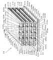
ここで、上述の図2に示した構成の3次元集積化装置20では、上記各集積回路基板27A,27B,27C,27Dは互いに上下に重なっている3組の22A1〜22D1,22A2〜22D2,22A3〜22D3、それぞれ個別に信号の授受が可能な通信チャンネルA、B、Cとして機能する構成について説明したが、本発明は、例えば、図4に示すように、リングバス構成を備える3次元集積化装置40に適用することもできる。Here, in the three-
この図4に示す3次元集積化装置40は、4枚の集積回路基板47A,47B,47C,47Dのうち、2つの集積回路基板上の開口部を共有し、集積回路基板間の信号の授受を行うリングバス構成としたものである。The three-
すなわち、この3次元集積化装置40は、それぞれ1つグランドプレーン41A,41B,41C,41Dを有し、当該グランドプレーン41A,41B,41C,41D上の所望の場所に2〜4個の開口部42A1,42A2,42B1〜42B4,42C1〜42C4,42D1,42D2が設けられ、この開口部42A1,42A2,42B1〜42B4,42C1〜42C4,42D1,42D2には上記グランドプレーン41A,41B,41C,41Dと対をなして形成されたそれぞれマイクロストリップライン43A1,43A2,43B1〜43B4,43C1〜43C4,43D1,43D2の各開放端部が位置され、上記各マイクロストリップライン43A1,43B2,43B3,43C1,43C4,43D2に接続され上記開口部42A1,42B2,42B3,42C1,42C4,42D2の周囲長λに略相当する周波数にて信号の送信を行う各送信部45A,45B2,45B1,45C1,45C2,45D及び上記各マイクロストリップライン43A2,43B1,43B4,43C2,43C3,43D1に接続され上記開口部42A2,42B1,42B4,42C2,42C3,42D1の周囲長λに略相当する周波数にて信号の受信を行う各受信部46A,46B1,46B2,46C2,46C1,46Dが設けられた4枚の集積回路基板47A,47B,47C,47Dを積層してなる。上記集積回路基板47Aの各開口部42A1,42A2は上記集積回路基板47Bの各開口部42B1,42B2と、上記集積回路基板47Bの各開口部42B3,42B4は上記集積回路基板47Cの各開口部42C3,42C4と、上記集積回路基板47Cの各開口部42C1,42C2は上記集積回路基板47Dの各開口部42D1,42D2と、それぞれ、各グランドプレーン41A,41B,41C,41Dと垂直な方向において互いに重なる位置に設けられている。That is, the three-
このような構成の3次元集積化装置40では、基本的に送信スロット、受信スロットを区別し、集積回路基板47Cと集積回路基板47DがスロットAで集積回路基板47Dから集積回路基板47Cへの信号伝送を行い、スロットBで集積回路基板47Cから集積回路基板47Dへの信号伝送を行う。 In the three-
この構成を図示の如く上下に繰り返すことで、リングバス構成をもった3次元集積化装置が実現される。Byrepeating this configurationup and down as shown in the figure, a three-dimensional integrated device having a ring bus configuration is realized.
さらに、このリングバス構成をもった3次元集積化装置40においても、図5に示すように、集積回路基板47A,47B,47C,47Dを構成するシリコン基板に上述の図3の(A),(B)に示したPBG構造と同様に導電性の貫通ビア29Bを設けた導電層29Aの周期構造29を作成することにより、ニアフィールドの磁界を遮断することができる。集積回路基板47A,47B,47C,47Dの開口部42A1,42A2,42B1〜42B4,42C1〜42C4,42D1,42D2に対応する部分のPBG構造は欠落させておくことにより、良好な信号伝送が実現でき、又、PBG構造によって、磁界の離散が抑制される為、チャネル間や、集積回路基板上の配線との干渉が抑えられる他、この集積化装置が搭載されるボード上の配線や、他の集積回路基板との干渉も抑制することができる。Further, also in the three-
10,20,40 3次元集積化装置、11A,11B,21A,21B,21C,21D,41A,41B,41C,41D グランドプレーン、12A,12B,22A1〜22A3,22B1〜22B3,22C1〜22C3,22D1〜22D3,42A1,42A2,42B1〜42B4,42C1〜42C4,42D1,42D2 開口部、13A,13B,23A1A,23A1B〜23A3A,23A3B,23B1A,23B3B〜23B3A,23B3B,23C1A,23C3B〜23C3A,23C3B,23D1A,23D1B〜23D3A,23D3B,43A1,43A2,43B1〜43B4,43C1〜43C4,43D1,43D2 マイクロストリップライン、14A,14B スイッチ、15A,15B,25A1A,〜25A3A,25B1A〜25B3A,25C1A〜25C3A,25D1A〜24D3A,45A,45B1,45B2,45C1,45C2,45D 送信部、16A,16B,26A1A,〜26A3A,26B1A〜26B3A,26C1A〜26C3A,26D1A〜26D3A,46A,46B1,46B2,46C1,46C2,46D 受信部、17A,17B,27A,27B,27C,27D,47A,47B,47C,47D 集積回路基板、27 シリコン基板、28 バンプ、29 周期構造、29A 導電層、29B 貫通ビア10, 20, 40 3D integrated device, 11A, 11B, 21A, 21B, 21C, 21D, 41A, 41B, 41C, 41D ground plane, 12A, 12B, 22A1 to 22A3 , 22B1 to 22B3 , 22C1 to 22C3 , 22D1 to 22D3 , 42A1 , 42A2 , 42B1 to 42B4 ,
Claims (3)
Translated fromJapanese各集積回路基板の各開口部は各グランドプレーンと垂直な方向において他の集積回路基板の開口部の少なくとも1つと重なっており、
上記各開口部には、それぞれ送信部が接続されたマイクロストリップラインと受信部が接続されたマイクロストリップラインの各一端が形成されており、上記各集積回路基板の1つが信号の送信側として機能するとき他の集積回路基板が受信側として機能し、上記各開口部の周囲長λ(媒質の比誘電率、比透磁率がそれぞれε、μの時λe=λ/√ε・μ)で共振する性質を持ち、上記各開口部の周囲長λに略相当するマイクロ波帯以上の周波数にて、上記各開口部を介して各集積回路基板間で信号を非接触で伝送する3次元集積化装置。Each has one or more ground planes, and one or more openings are provided at desired locations on the ground plane. Microstrip line pairs formed with the ground plane are formed in the openings. At least two pieces of transmission units and / or reception units that are located at the ends and are connected to the microstrip line and perform signal transmission and / or reception at a frequency substantially corresponding to the circumferential length λ of the opening are provided. Stacked integrated circuit boards,
Each opening of each integrated circuit board overlaps at least one of the openings of another integrated circuit board in a direction perpendicular to each ground plane,
Each opening is formed with one end of a microstrip line to which a transmission unit is connected and a microstrip line to which a reception unit is connected, and one of the integrated circuit boards functions as a signal transmission side. When the other integrated circuit boardfunctions as the receiving side,it resonates at the peripheral length λ of each opening (λe = λ / √ε · μ when the relative permittivity and relative permeability of the medium are ε and μ, respectively) 3D integration that transmits signals between each integrated circuit board in a non-contact manner through each opening at a frequency equal to or higher than the microwave band corresponding to the peripheral length λ of each opening. Equipment .
Priority Applications (3)
| Application Number | Priority Date | Filing Date | Title |
|---|---|---|---|
| JP2006069545AJP4325630B2 (en) | 2006-03-14 | 2006-03-14 | 3D integration device |
| US11/715,161US8089107B2 (en) | 2006-03-14 | 2007-03-07 | Three-dimensional integrated device |
| KR1020070024246AKR101350653B1 (en) | 2006-03-14 | 2007-03-13 | Three-dimensional integrated device |
Applications Claiming Priority (1)
| Application Number | Priority Date | Filing Date | Title |
|---|---|---|---|
| JP2006069545AJP4325630B2 (en) | 2006-03-14 | 2006-03-14 | 3D integration device |
Publications (2)
| Publication Number | Publication Date |
|---|---|
| JP2007251394A JP2007251394A (en) | 2007-09-27 |
| JP4325630B2true JP4325630B2 (en) | 2009-09-02 |
Family
ID=38516883
Family Applications (1)
| Application Number | Title | Priority Date | Filing Date |
|---|---|---|---|
| JP2006069545AExpired - Fee RelatedJP4325630B2 (en) | 2006-03-14 | 2006-03-14 | 3D integration device |
Country Status (3)
| Country | Link |
|---|---|
| US (1) | US8089107B2 (en) |
| JP (1) | JP4325630B2 (en) |
| KR (1) | KR101350653B1 (en) |
Families Citing this family (26)
| Publication number | Priority date | Publication date | Assignee | Title |
|---|---|---|---|---|
| JP4676238B2 (en)* | 2005-04-18 | 2011-04-27 | 株式会社日立製作所 | Backplane bus main board, and router system and storage system using the same |
| US8348967B2 (en)* | 2007-07-27 | 2013-01-08 | Ethicon Endo-Surgery, Inc. | Ultrasonic surgical instruments |
| EP2217157A2 (en) | 2007-10-05 | 2010-08-18 | Ethicon Endo-Surgery, Inc. | Ergonomic surgical instruments |
| US8168891B1 (en)* | 2007-10-26 | 2012-05-01 | Force10 Networks, Inc. | Differential trace profile for printed circuit boards |
| US10010339B2 (en)* | 2007-11-30 | 2018-07-03 | Ethicon Llc | Ultrasonic surgical blades |
| US8415777B2 (en)* | 2008-02-29 | 2013-04-09 | Broadcom Corporation | Integrated circuit with millimeter wave and inductive coupling and methods for use therewith |
| JP5050986B2 (en)* | 2008-04-30 | 2012-10-17 | ソニー株式会社 | Communications system |
| JP4643691B2 (en)* | 2008-07-31 | 2011-03-02 | 株式会社日立製作所 | Semiconductor integrated circuit device |
| US9089360B2 (en)* | 2008-08-06 | 2015-07-28 | Ethicon Endo-Surgery, Inc. | Devices and techniques for cutting and coagulating tissue |
| JP4977101B2 (en)* | 2008-08-26 | 2012-07-18 | 株式会社東芝 | Multilayer semiconductor device |
| JP5526659B2 (en)* | 2008-09-25 | 2014-06-18 | ソニー株式会社 | Millimeter-wave dielectric transmission device |
| JP5216532B2 (en)* | 2008-10-30 | 2013-06-19 | 株式会社日立製作所 | Semiconductor integrated circuit |
| US8650728B2 (en) | 2009-06-24 | 2014-02-18 | Ethicon Endo-Surgery, Inc. | Method of assembling a transducer for a surgical instrument |
| US8663220B2 (en)* | 2009-07-15 | 2014-03-04 | Ethicon Endo-Surgery, Inc. | Ultrasonic surgical instruments |
| KR101007288B1 (en)* | 2009-07-29 | 2011-01-13 | 삼성전기주식회사 | Printed Circuit Boards and Electronics |
| CN102598262A (en)* | 2009-11-10 | 2012-07-18 | 日本电气株式会社 | Semiconductor device and noise suppression method |
| KR101686582B1 (en)* | 2009-12-22 | 2016-12-15 | 삼성전자주식회사 | Stacked electronic device having inductive coupling communication unit between stacked chips |
| US8469981B2 (en)* | 2010-02-11 | 2013-06-25 | Ethicon Endo-Surgery, Inc. | Rotatable cutting implement arrangements for ultrasonic surgical instruments |
| US8531064B2 (en)* | 2010-02-11 | 2013-09-10 | Ethicon Endo-Surgery, Inc. | Ultrasonically powered surgical instruments with rotating cutting implement |
| WO2012051340A1 (en)* | 2010-10-12 | 2012-04-19 | Analog Devices, Inc. | Microphone package with embedded asic |
| KR101152823B1 (en) | 2010-12-30 | 2012-06-12 | 에스케이하이닉스 주식회사 | Semiconductor chip and stacked semiconductor package having the same |
| JP5644521B2 (en)* | 2011-01-14 | 2014-12-24 | ソニー株式会社 | Signal transmission device and electronic device |
| US9679828B2 (en) | 2012-01-31 | 2017-06-13 | Amit Verma | System-on-chip electronic device with aperture fed nanofilm antenna |
| CN104937768B (en)* | 2012-12-27 | 2018-06-08 | 韩国科学技术院 | Low-power, high-speed multi-channel chip-to-chip interface using dielectric waveguides |
| CN108370083B (en)* | 2015-09-25 | 2021-05-04 | 英特尔公司 | Antenna for platform level wireless interconnect |
| JP7160012B2 (en)* | 2019-10-03 | 2022-10-25 | 株式会社デンソー | electronic controller |
Family Cites Families (16)
| Publication number | Priority date | Publication date | Assignee | Title |
|---|---|---|---|---|
| JPS6459845A (en) | 1987-08-31 | 1989-03-07 | Toshiba Corp | Semiconductor device |
| US5701037A (en) | 1994-11-15 | 1997-12-23 | Siemens Aktiengesellschaft | Arrangement for inductive signal transmission between the chip layers of a vertically integrated circuit |
| US5786979A (en) | 1995-12-18 | 1998-07-28 | Douglass; Barry G. | High density inter-chip connections by electromagnetic coupling |
| FR2743199B1 (en)* | 1996-01-03 | 1998-02-27 | Europ Agence Spatiale | RECEIVE AND / OR TRANSMITTER FLAT MICROWAVE NETWORK ANTENNA AND ITS APPLICATION TO THE RECEPTION OF GEOSTATIONARY TELEVISION SATELLITES |
| KR100207600B1 (en)* | 1997-03-31 | 1999-07-15 | 윤종용 | Cavity-backed microstrip dipole antenna array |
| JP3462062B2 (en) | 1997-12-22 | 2003-11-05 | 京セラ株式会社 | Connection structure of high-frequency transmission line and wiring board |
| JP3965762B2 (en) | 1998-03-13 | 2007-08-29 | 日立化成工業株式会社 | Triplate line interlayer connector |
| JP2000058691A (en)* | 1998-08-07 | 2000-02-25 | Sharp Corp | Millimeter-wave semiconductor device |
| US6717229B2 (en)* | 2000-01-19 | 2004-04-06 | Fabtech, Inc. | Distributed reverse surge guard |
| US7247932B1 (en)* | 2000-05-19 | 2007-07-24 | Megica Corporation | Chip package with capacitor |
| JP2001352206A (en)* | 2000-06-07 | 2001-12-21 | Mitsubishi Electric Corp | High frequency circuit device |
| JP2002198742A (en) | 2000-12-25 | 2002-07-12 | New Japan Radio Co Ltd | Multiplier |
| US6882239B2 (en)* | 2001-05-08 | 2005-04-19 | Formfactor, Inc. | Electromagnetically coupled interconnect system |
| US6627992B2 (en)* | 2001-05-21 | 2003-09-30 | Xytrans, Inc. | Millimeter wave (MMW) transceiver module with transmitter, receiver and local oscillator frequency multiplier surface mounted chip set |
| US6888420B2 (en)* | 2002-11-14 | 2005-05-03 | Hrl Laboratories, Llc | RF MEMS switch matrix |
| US7352056B2 (en)* | 2004-10-13 | 2008-04-01 | Advanced Semiconductor Engineering, Inc. | Semiconductor package structure with microstrip antennan |
- 2006
- 2006-03-14JPJP2006069545Apatent/JP4325630B2/ennot_activeExpired - Fee Related
- 2007
- 2007-03-07USUS11/715,161patent/US8089107B2/ennot_activeExpired - Fee Related
- 2007-03-13KRKR1020070024246Apatent/KR101350653B1/ennot_activeExpired - Fee Related
Also Published As
| Publication number | Publication date |
|---|---|
| KR20070093838A (en) | 2007-09-19 |
| JP2007251394A (en) | 2007-09-27 |
| US8089107B2 (en) | 2012-01-03 |
| US20070215913A1 (en) | 2007-09-20 |
| KR101350653B1 (en) | 2014-01-10 |
Similar Documents
| Publication | Publication Date | Title |
|---|---|---|
| JP4325630B2 (en) | 3D integration device | |
| US9514879B2 (en) | Signal transmission through LC resonant circuits | |
| US8704627B2 (en) | Inductor element, integrated circuit device, and three-dimensional circuit device | |
| US8994470B2 (en) | Circuit substrate having noise suppression structure | |
| JP5512885B2 (en) | Through-via inductors or transformers on high-resistance boards with programmability | |
| KR100838246B1 (en) | Printed Circuit Board with Electromagnetic Bandgap Structure | |
| CN106206539B (en) | Interconnection wiring configuration | |
| NL2029704B1 (en) | Device-to-device communication system, packages, and package system | |
| KR100981143B1 (en) | Integrated circuit antenna structure | |
| KR101587331B1 (en) | Package structures and method of forming package structures | |
| JP2007036722A (en) | Semiconductor device | |
| US20180212306A1 (en) | Antennas for platform level wireless interconnects | |
| JP6658704B2 (en) | Antenna module | |
| EP2860757B1 (en) | Integrated circuit | |
| CN112310627A (en) | Antenna device | |
| Pano et al. | TSV antennas for multi-band wireless communication | |
| KR101046716B1 (en) | Electromagnetic bandgap structures and circuit boards | |
| CN103260340A (en) | Multilayered wiring substrate and electronic apparatus | |
| US11357099B2 (en) | RF package module and electronic device comprising RF package module | |
| WO2012176933A1 (en) | Noise suppression device and multilayer printed circuit board carrying same | |
| JP5054413B2 (en) | Antenna element and semiconductor device | |
| CN105514082A (en) | Inter-chip wireless interconnection structure | |
| TWI602266B (en) | Embedded packages, methods of fabricating the same, electronic systems including the same, and memory cards including the same | |
| EP4033608B1 (en) | Antenna structure and electronic device comprising same | |
| CN108966480B (en) | High frequency system, communication link |
Legal Events
| Date | Code | Title | Description |
|---|---|---|---|
| A977 | Report on retrieval | Free format text:JAPANESE INTERMEDIATE CODE: A971007 Effective date:20071227 | |
| A131 | Notification of reasons for refusal | Free format text:JAPANESE INTERMEDIATE CODE: A131 Effective date:20090217 | |
| A521 | Request for written amendment filed | Free format text:JAPANESE INTERMEDIATE CODE: A523 Effective date:20090420 | |
| TRDD | Decision of grant or rejection written | ||
| A01 | Written decision to grant a patent or to grant a registration (utility model) | Free format text:JAPANESE INTERMEDIATE CODE: A01 Effective date:20090519 | |
| A01 | Written decision to grant a patent or to grant a registration (utility model) | Free format text:JAPANESE INTERMEDIATE CODE: A01 | |
| A61 | First payment of annual fees (during grant procedure) | Free format text:JAPANESE INTERMEDIATE CODE: A61 Effective date:20090601 | |
| FPAY | Renewal fee payment (event date is renewal date of database) | Free format text:PAYMENT UNTIL: 20120619 Year of fee payment:3 | |
| FPAY | Renewal fee payment (event date is renewal date of database) | Free format text:PAYMENT UNTIL: 20120619 Year of fee payment:3 | |
| FPAY | Renewal fee payment (event date is renewal date of database) | Free format text:PAYMENT UNTIL: 20120619 Year of fee payment:3 | |
| FPAY | Renewal fee payment (event date is renewal date of database) | Free format text:PAYMENT UNTIL: 20130619 Year of fee payment:4 | |
| R250 | Receipt of annual fees | Free format text:JAPANESE INTERMEDIATE CODE: R250 | |
| R250 | Receipt of annual fees | Free format text:JAPANESE INTERMEDIATE CODE: R250 | |
| LAPS | Cancellation because of no payment of annual fees |