JP4318913B2 - Application processing equipment - Google Patents
Application processing equipmentDownload PDFInfo
- Publication number
- JP4318913B2 JP4318913B2JP2002376233AJP2002376233AJP4318913B2JP 4318913 B2JP4318913 B2JP 4318913B2JP 2002376233 AJP2002376233 AJP 2002376233AJP 2002376233 AJP2002376233 AJP 2002376233AJP 4318913 B2JP4318913 B2JP 4318913B2
- Authority
- JP
- Japan
- Prior art keywords
- wafer
- substrate
- coating
- cup
- processed
- Prior art date
- Legal status (The legal status is an assumption and is not a legal conclusion. Google has not performed a legal analysis and makes no representation as to the accuracy of the status listed.)
- Expired - Fee Related
Links
Images


Classifications
- H—ELECTRICITY
- H01—ELECTRIC ELEMENTS
- H01L—SEMICONDUCTOR DEVICES NOT COVERED BY CLASS H10
- H01L21/00—Processes or apparatus adapted for the manufacture or treatment of semiconductor or solid state devices or of parts thereof
- H01L21/67—Apparatus specially adapted for handling semiconductor or electric solid state devices during manufacture or treatment thereof; Apparatus specially adapted for handling wafers during manufacture or treatment of semiconductor or electric solid state devices or components ; Apparatus not specifically provided for elsewhere
- H01L21/67005—Apparatus not specifically provided for elsewhere
- H01L21/67011—Apparatus for manufacture or treatment
- H01L21/6715—Apparatus for applying a liquid, a resin, an ink or the like
- G—PHYSICS
- G03—PHOTOGRAPHY; CINEMATOGRAPHY; ANALOGOUS TECHNIQUES USING WAVES OTHER THAN OPTICAL WAVES; ELECTROGRAPHY; HOLOGRAPHY
- G03F—PHOTOMECHANICAL PRODUCTION OF TEXTURED OR PATTERNED SURFACES, e.g. FOR PRINTING, FOR PROCESSING OF SEMICONDUCTOR DEVICES; MATERIALS THEREFOR; ORIGINALS THEREFOR; APPARATUS SPECIALLY ADAPTED THEREFOR
- G03F7/00—Photomechanical, e.g. photolithographic, production of textured or patterned surfaces, e.g. printing surfaces; Materials therefor, e.g. comprising photoresists; Apparatus specially adapted therefor
- G03F7/16—Coating processes; Apparatus therefor
- G03F7/162—Coating on a rotating support, e.g. using a whirler or a spinner
- H—ELECTRICITY
- H01—ELECTRIC ELEMENTS
- H01L—SEMICONDUCTOR DEVICES NOT COVERED BY CLASS H10
- H01L21/00—Processes or apparatus adapted for the manufacture or treatment of semiconductor or solid state devices or of parts thereof
- H01L21/67—Apparatus specially adapted for handling semiconductor or electric solid state devices during manufacture or treatment thereof; Apparatus specially adapted for handling wafers during manufacture or treatment of semiconductor or electric solid state devices or components ; Apparatus not specifically provided for elsewhere
- H01L21/67005—Apparatus not specifically provided for elsewhere
- H01L21/67011—Apparatus for manufacture or treatment
- H01L21/67017—Apparatus for fluid treatment
Landscapes
- Engineering & Computer Science (AREA)
- Physics & Mathematics (AREA)
- General Physics & Mathematics (AREA)
- Condensed Matter Physics & Semiconductors (AREA)
- Manufacturing & Machinery (AREA)
- Computer Hardware Design (AREA)
- Microelectronics & Electronic Packaging (AREA)
- Power Engineering (AREA)
- Coating Apparatus (AREA)
- Exposure Of Semiconductors, Excluding Electron Or Ion Beam Exposure (AREA)
- Materials For Photolithography (AREA)
Description
Translated fromJapanese【0001】
【発明が属する技術分野】
本発明は、被処理基板に塗布膜を形成する塗布処理装置に関する。
【0002】
【従来の技術】
例えば、半導体デバイスの製造工程においては、所謂、フォトリソグラフィー技術を用いて、半導体ウエハに所定の回路パターンを形成している。このフォトリソグラフィー工程においては、ウエハにレジスト膜を形成し、このレジスト膜を所定のパターンで露光し、露光処理されたウエハを現像処理することによって、回路パターンが形成される。
【0003】
ここで、ウエハにレジスト膜を形成する方法としては、略水平姿勢で保持されたウエハの中心部に所定量のレジスト液を供給した後に、ウエハを高速回転させることによってレジスト液をウエハ全体に拡げる、所謂、スピンコート法が広く用いられている。このようなスピンコート法による成膜を行う装置として、例えば、特開2001−189266号公報(特許文献1)には、ウエハの周囲を囲うように配置され、底部から強制的に排気を行うことによって、ウエハの周囲の雰囲気を強制的に排気する処理カップと、この処理カップの内側においてウエハの外周を囲うように配置され、ウエハ付近に生ずる気流を制御する気流制御板と、を有する塗布処理装置が開示されている。
【0004】
【特許文献1】
特開2001−189266号公報(第3頁−第4頁、第1図)
【0005】
【発明が解決しようとする課題】
しかし、このような塗布処理装置においては、排気流路の雰囲気採取口がウエハの端面の近傍に位置しているために、ウエハの端面が排気流路に流れ込む気流によってウエハの周縁部でのレジスト液の乾燥が速くなる。この場合には、ウエハの中心から周縁に向かって流れるレジスト液がウエハの周縁で堆積しやすくなるために、レジスト膜の厚さがウエハの周縁部では中央部よりも厚くなる。近年、回路パターンの微細化と高集積化が進むにつれて形成すべきレジスト膜の厚さが薄くなってきており、僅かなレジスト膜の厚さの不均一が製造歩留まりと製品の品質に大きな影響を与えるようになってきている。
【0006】
本発明はこのような事情に鑑みてなされたものであり、厚さの均一性に優れた塗布膜の形成を可能とする塗布処理装置を提供することを目的とする。
【0007】
【課題を解決するための手段】
すなわち、本発明の第1の観点によれば、被処理基板に所定の塗布液を供給して前記被処理基板を回転することにより前記塗布液を拡げて厚さ分布の均一な塗布膜を形成する塗布処理装置であって、表面に塗布液が供給される被処理基板を略水平姿勢で保持する保持手段と、前記被処理基板を水平面内で回転させる回転手段と、前記保持手段を収容し、底部から排気を行うことによって前記被処理基板の周囲の雰囲気を排気する処理容器と、を具備し、前記処理容器は、筒状の鉛直壁および前記鉛直壁の上端に連設されて内側上方に傾倒した傾斜壁とからなる側壁部を有し、前記側壁部が前記被処理基板の外側を囲うように配置された第1カップと、前記第1カップの内側において前記被処理基板に近接して前記被処理基板を囲うように配置され、断面略三角形で上に凸である上リング部および断面略三角形で下に凸である下リング部から構成された断面略四角形の気流制御部材と、を有し、実質的に前記被処理基板の周囲の雰囲気を排気する排気流路が前記第1カップの側壁部と前記気流制御部材との間に形成され、前記排気流路における雰囲気採取口が前記被処理基板の外方上部に位置し、前記雰囲気採取口が、前記第1カップの上端部と前記気流制御部材の頂点との間に形成されていることを特徴とする塗布処理装置、が提供される。
【0009】
このような塗布処理装置によれば、基板の周囲の雰囲気を排気するに際して、排気される気流の基板の周縁部への影響を小さくすることができる。これによって、基板全体で厚さ分布の均一な塗布膜を形成することができる。
【0010】
【発明の実施の形態】
以下、本発明の実施の形態について図面を参照しながら説明する。ここでは、半導体ウエハにレジスト膜を塗布して塗布膜を形成するレジスト塗布処理ユニットを備え、レジスト膜の形成から現像処理までの一連の処理を行うレジスト塗布・現像処理装置を例に挙げることとする。
【0011】
図1は、レジスト塗布・現像処理システム1を示す概略平面図、図2はその正面図、図3はその背面図である。レジスト塗布・現像処理システム1は、搬送ステーションであるカセットステーション10と、複数の処理ユニットを有する処理ステーション11と、処理ステーション11に隣接して設けられる図示しない露光装置との間でウエハWを受け渡すためのインターフェイスステーション12と、を具備している。
【0012】
カセットステーション10は、ウエハWを複数枚(例えば25枚)収容可能なウエハカセットCRを載置するカセット載置台20を有している。レジスト塗布・現像処理システム1において処理すべきウエハWが収容されたウエハカセットCRは、他のシステムからカセットステーション10のカセット載置台20へ搬入され、逆に、レジスト塗布・現像処理システム1における処理を終えたウエハWが収容されたウエハWが収容されたウエハカセットCRは、カセット載置台20から他のシステムへ搬出される。
【0013】
カセット載置台20上には、図1中X方向に沿って複数(図では4個)の位置決め突起20aが形成されており、位置決め突起20aの位置にウエハカセットCRがそれぞれのウエハ出入口を処理ステーション11側に向けて1列に載置可能となっている。ウエハカセットCRにおいてはウエハWが鉛直方向(Z方向)に配列されている。
【0014】
カセットステーション10はまた、カセット載置台20と処理ステーション11との間にウエハ搬送機構21を備えている。このウエハ搬送機構21は、カセット配列方向(X方向)およびその中のウエハWの配列方向(Z方向)に移動可能であり、かつ、図1中に示されるθ方向に回転可能なウエハ搬送用ピック21aを有している。こうしてウエハ搬送用ピック21aは、カセット載置台20に載置されたウエハカセットCRの所定位置に収容されたウエハWに対して選択的にアクセスすることができ、また、後述する処理ステーション11側の第3の処理部G3に属するアライメントユニット(ALIM)およびエクステンションユニット(EXT)にもアクセスできるようになっている。
【0015】
処理ステーション11は、ウエハWに対してレジスト液の塗布および現像を行う際の一連の工程を実施するための複数の処理ユニットを備え、これらが所定位置に多段に配置されている。各処理ユニットにおいてウエハWは1枚ずつ処理される。この処理ステーション11は、図1に示すように、中心部にウエハ搬送路22aを有しており、この中に主ウエハ搬送機構22が設けられ、ウエハ搬送路22aの周りに全ての処理ユニットが配置された構成となっている。これら複数の処理ユニットは、複数の処理部に分かれており、各処理部は複数の処理ユニットが鉛直方向(Z方向)に沿って多段に配置されている。
【0016】
主ウエハ搬送機構22は、図3に示すように、筒状支持体79の内側にウエハ搬送装置76を鉛直方向(Z方向)に昇降自在に装備している。筒状支持体79は図示しないモータの回転駆動力によって回転可能となっており、それに伴ってウエハ搬送装置76も一体的に回転可能となっている。ウエハ搬送装置76は、搬送基台77の前後方向に移動自在な複数本の保持アーム78を備え、これらの保持アーム78によって各処理ユニット間でのウエハWの受け渡しを実現している。
【0017】
図1に示すように、レジスト塗布・現像処理システム1においては、4個の処理部G1・G2・G3・G4がウエハ搬送路22aの周囲に実際に配置されている。これらのうち、第1および第2の処理部G1・G2はレジスト塗布・現像処理システム1の正面側(図1における手前側)に並列に配置され、第3の処理部G3はカセットステーション10に隣接して配置され、第4の処理部G4はインターフェイスステーション12に隣接して配置されている。また、レジスト塗布・現像処理システム1においては、背面部に第5の処理部G5を配置することができるようになっている。
【0018】
第1の処理部G1では、コータカップ(CP)内でウエハWを図示しないスピンチャックに乗せて所定の処理を行う2台のスピナ型処理ユニットであるレジスト塗布処理ユニット(COT)およびレジストのパターンを現像する現像処理ユニット(DEV)が下から順に2段に重ねられている。第2の処理部G2も同様に、2台のスピナ型処理ユニットとしてレジスト塗布処理ユニット(COT)および現像処理ユニット(DEV)が下から順に2段に重ねられている。なお、レジスト塗布処理ユニット(COT)の構造については後に詳細に説明する。
【0019】
第3の処理部G3においては、図3に示すように、ウエハWを載置台SPに載せて所定の処理を行うオーブン型の処理ユニットが多段に重ねられている。すなわち、レジストの定着性を高めるためのいわゆる疎水化処理を行うアドヒージョンユニット(AD)、位置合わせを行うアライメントユニット(ALIM)、ウエハWの搬入出を行うエクステンションユニット(EXT)、冷却処理を行うクーリングプレートユニット(COL)、レジスト液が塗布されたウエハWまたは露光処理後のウエハWに対して加熱処理を行う4つのホットプレートユニット(HP)が下から順に8段に重ねられている。なお、アライメントユニット(ALIM)の代わりにクーリングプレートユニット(COL)を設け、クーリングプレートユニット(COL)にアライメント機能を持たせてもよい。
【0020】
第4の処理部G4においても、オーブン型の処理ユニットが多段に重ねられている。すなわち、クーリングプレートユニット(COL)、クーリングプレートを備えたウエハ搬入出部であるエクステンション・クーリングプレートユニット(EXTCOL)、エクステンションユニット(EXT)、クーリングプレートユニット(COL)、および4つのホットプレートユニット(HP)が下から順に8段に重ねられている。
【0021】
主ウエハ搬送機構22の背部側に第5の処理部G5を設ける場合に、第5の処理部G5は、案内レール25に沿って主ウエハ搬送機構22から見て側方へ移動できるようになっている。これにより、第5の処理部G5を設けた場合でも、これを案内レール25に沿ってスライドすることによって空間部が確保されるために、主ウエハ搬送機構22に対して背後からメンテナンス作業を容易に行うことができる。
【0022】
インターフェイスステーション12は、奥行方向(X方向)については、処理ステーション11と同じ長さを有している。図1、図2に示すように、このインターフェイスステーション12の正面部には、可搬性のピックアップカセットPRと定置型のバッファカセットBRが2段に配置され、背面部には周辺露光装置23が配設され、中央部にはウエハ搬送機構24が配設されている。このウエハ搬送機構24はウエハ搬送用アーム24aを有しており、このウエハ搬送用アーム24aは、X方向、Z方向に移動して両カセットPR・BRおよび周辺露光装置23にアクセス可能となっている。
【0023】
なお、ウエハ搬送用アーム24aはθ方向に回転可能であり、処理ステーション11の第4の処理部G4に属するエクステンションユニット(EXT)や、さらには隣接する露光装置側のウエハ受け渡し台(図示せず)にもアクセス可能となっている。
【0024】
上述したレジスト塗布・現像処理システム1においては、まず、カセットステーション10において、ウエハ搬送機構21のウエハ搬送用ピック21aがカセット載置台20上の未処理のウエハWを収容しているウエハカセットCRにアクセスして1枚のウエハWを取り出し、第3の処理部G3のエクステンションユニット(EXT)に搬送する。
【0025】
ウエハWは、このエクステンションユニット(EXT)から、主ウエハ搬送機構22のウエハ搬送装置76により、処理ステーション11に搬入される。そして、第3の処理部G3のアライメントユニット(ALIM)によりアライメントされた後、アドヒージョン処理ユニット(AD)に搬送され、そこでレジストの定着性を高めるための疎水化処理(HMDS処理)が施される。この処理は加熱を伴うため、その後ウエハWは、ウエハ搬送装置76によりクーリングプレートユニット(COL)に搬送されて冷却される。
【0026】
アドヒージョン処理ユニット(AD)での処理が終了してクーリングプレートユニット(COL)で冷却されたウエハW、またはアドヒージョン処理ユニット(AD)での処理を行わないウエハWは、引き続き、ウエハ搬送装置76によりレジスト塗布処理ユニット(COT)に搬送され、そこでレジストが塗布され、レジスト膜(塗布膜)が形成される。塗布処理終了後、ウエハWは、第3の処理部G3または第4の処理部G4のホットプレートユニット(HP)へ搬送されて、そこでプリベーク処理され、次いでいずれかのクーリングプレートユニット(COL)に搬送されて、そこで冷却される。
【0027】
冷却されたウエハWは、第3の処理部G3のアライメントユニット(ALIM)に搬送され、そこでアライメントされた後、第4の処理部G4のエクステンションユニット(EXT)を介してインターフェイスステーション12に搬送される。
【0028】
ウエハWは、インターフェイスステーション12において周辺露光装置23により周辺露光されて余分なレジストが除去された後、インターフェイスステーション12に隣接して設けられた図示しない露光装置に搬送され、そこで所定のパターンにしたがってウエハWのレジスト膜に露光処理が施される。
【0029】
露光後のウエハWは、再びインターフェイスステーション12に戻され、ウエハ搬送機構24により、第4の処理部G4に属するエクステンションユニット(EXT)に搬送される。そしてウエハWは、ウエハ搬送装置76により第3の処理部G3または第4の処理部G4のホットプレートユニット(HP)へ搬送されて、そこでポストエクスポージャーベーク処理が施される。ポストエクスポージャーベーク処理においては、ウエハWは所定温度まで冷却されるが、ウエハWはその後に必要に応じてクーリングプレートユニット(COL)に搬送され、そこでさらに冷却処理される。
【0030】
その後、ウエハWは現像処理ユニット(DEV)に搬送され、そこで露光パターンの現像が行われる。現像終了後、ウエハWは第3の処理部G3のホットプレートユニット(HP)へ搬送されて、そこでポストベーク処理が施される。このような一連の処理が終了したウエハWは、第3の処理部G3のエクステンションユニット(EXT)を介してカセットステーション10に戻され、いずれかのウエハカセットCRに収容される。
【0031】
次に、レジスト塗布処理ユニット(COT)について詳細に説明する。図4はレジスト塗布処理ユニット(COT)の概略構造を示す断面図であり、図5は図4中の領域Aの拡大図である。レジスト塗布処理ユニット(COT)は、ウエハWを略水平姿勢で保持するスピンチャック41と、スピンチャック41を回転させる回転機構42と、スピンチャック41を昇降させる昇降機構43と、スピンチャック41を収容する処理カップ50とを具備している。処理カップ50の上方からは、図示しないフィルターファンユニット(FFU)から清浄な空気がダウンフローとして処理カップ50に向けて供給されるようになっている。
【0032】
スピンチャック41に保持されたウエハWの表面にレジスト液を供給するレジスト塗布ノズル91は、ノズル保持アーム92に保持されている。ノズル保持アーム92は、スライド機構や回動機構等の水平方向移動機構と昇降機構(鉛直方向移動機構)とからなるノズル移動機構93によってウエハWの中心部と処理容器の外側の待避位置(図示せず)との間で移動自在であり、かつ、ウエハWの表面に近接または離隔自在となっている。なお、レジスト塗布ノズル91には、レジスト液がレジスト送液装置94から送られるようになっている。
【0033】
スピンチャック41は、図示しない吸引機構によってウエハWを減圧吸着して保持することができるようになっている。スピンチャック41にウエハWを吸着保持し、ウエハWのほぼ中心に所定量のレジスト液を供給した後にスピンチャック41を回転機構42によって回転させることにより、ウエハWにレジスト膜が形成される。このとき、ウエハWから周囲に飛散する余分なレジスト液を処理カップ50によって回収する。
【0034】
処理カップ50は、大略的に、ウエハWの外側を囲うように配置された第1カップ51と、第1カップ51の内側においてウエハWに近接してウエハWを囲うように配置された気流制御部材52と、ウエハWの下側に配置された第2カップ53から構成されている。
【0035】
第1カップ51は、筒状の第1鉛直壁71aおよびこの第1鉛直壁71aの上端に連設されて内側上方に向けて傾倒した第1傾斜壁71bからなる外周壁61aと、第1鉛直壁71aの内側に設けられた円筒状の中間壁61bと、底壁61cとを有している。気流制御部材52は、断面略三角形で上に凸である上リング部材62aおよび断面略三角形で下に凸である下リング部材62bから構成された断面略四角形の形状を有している。上リング部材62aと下リング部材62bは一体的に構成されていてもよい。第2カップ53は、ウエハWの下側から斜め下に外方に向けて拡がる第2傾斜壁63aと、この第2傾斜壁63aの下端に連通する筒状の第2鉛直壁63bと、第1カップ51の中間壁61bの内側に配置された円筒状の内周壁63cとを有している。
【0036】
処理カップ50においては、外周壁61aと気流制御部材52との間に排気流路55が、下リング部材62bと第2傾斜壁63aとの間に排液流路56が、第1鉛直壁71aと第2鉛直壁63bとの間に排気流路55と排液流路56が合流する排気/排液流路57が、外周壁61aと中間壁61bとの間に排液室58が、中間壁61bと内周壁63cとの間に排気室59が、それぞれ形成されている。また、底壁61cには、排液室58が形成されている部分において排液口74が、排気室59が形成されている部分において排気口72がそれぞれ形成されており、排液口74には排液管75が、排気口72には排気管73が、それぞれ取り付けられている。
【0037】
排気管73の下流には図示しない排気装置が設けられており、ウエハWの周囲の雰囲気は、この排気装置を稼働するすることによって排気口72を通して底部から排気される。レジスト塗布処理ユニット(COT)においては、このウエハWの周囲の雰囲気の排気は実質的に排気流路55を通して行われ、ウエハWを回転させた際にウエハWから振り切られるレジスト液の排液は実質的に排液流路56を通して行われる。次にこのことについてさらに詳細に説明する。
【0038】
図5に示されるように、排気流路55における排気の採り入れ口(以下、雰囲気採取口という)55aは、第1カップ51の第1傾斜壁71bの上端部と気流制御部材52の上リング部材62aの頂点との間に形成され、この雰囲気採取口55aはウエハWの外方上部に位置している。また、排液流路56へレジスト液が流れ込むためのレジスト液採取口56aは、ウエハWと気流制御部材52との間に形成されている。
【0039】
気流制御部材52がウエハWに近接して配置されているために、レジスト液採取口56aの幅(γ)は雰囲気採取口55aの幅(α1)よりも狭くなっている。このために、ウエハWの周辺の雰囲気は、雰囲気採取口55aから排気流路55へと流れ込みやすく、逆にレジスト液採取口56aを通して排液流路56へは流れ込み難くなる。このようにして実質的にウエハWの周辺の雰囲気の排気は排気流路55を通して行われるようになる。
【0040】
排気流路55に気流が流れ込む際には、雰囲気採取口55aの近傍で強い排気気流が発生する。しかし、雰囲気採取口55aはウエハWから離れた位置に形成されているために、排気流路55に流れ込む排気気流のウエハWの周縁部への影響は小さくなる。また、レジスト液採取口56aへは気流が流れ込み難いから、レジスト液採取口56aの近傍では強い排気気流は発生しなくなる。こうしてレジスト塗布処理ユニット(COT)を用いたレジスト膜の成膜工程においては、排気気流によるレジスト膜の周縁部の乾燥が抑制されるため、膜厚分布の均一性に優れたレジスト膜を得ることができる。
【0041】
このような効果を実効的に得るために、好ましくは、スピンチャック41を回転させた際にウエハWから振り切られたレジスト液は実質的に下リング部材62bの内側の傾斜面に衝突することによって排液流路56に導かれるように、また、ウエハWの周縁部の近傍を流れる気流は実質的に上リング部材62aの内側の傾斜面に沿って上昇した後に雰囲気採取口55aから排気流路55に流れ込むように、気流制御部材52は、上リング部材62aの内側の角と下リング部材62bの内側の角とが合わされて形成される頂点の高さ位置が、スピンチャック41に保持されたウエハWの表面の高さ位置よりも、例えば0.1mm〜1mm程度高くなるように配置される。また、気流制御部材52は、気流制御部材52の頂点(上リング部材62aの頂点)が第1カップ51の頂点(第1傾斜壁71bの最上部)よりも低い位置にくるように、配置される。
【0042】
気流制御部材52を構成する上リング部材62aの内側の底角θ1は、24度以上34度以下とすることが好ましい。上リング部材62aの底角θ1がこの範囲の値よりも小さくなると、雰囲気採取口55aの位置が下がってウエハWに近づくために排気流路55に流れ込む気流のウエハWの周縁部への影響が大きくなり、これによってウエハWの周縁部でレジスト膜が厚くなり易くなる。逆に、上リング部材62aの底角θ1がこの範囲の値よりも大きくなると、ウエハWの中央部から外周に向かう気流が上リング部材62aの内側の傾斜面に衝突して中央部に戻るような気流が発生し易くなるため、この気流に含まれるレジスト液のミストがレジスト膜に付着してレジスト膜が汚染され易くなる。
【0043】
上リング部材62aの外側の底角θ3は、排気流路55に一定の幅が確保されるように第1傾斜壁71bの傾斜角度に適合させて定められ、例えば、22度以上32度以下の範囲とすることができる。また、気流制御部材52の内径および外径は処理するウエハWの直径によって変化するため、上リング部材62aの高さもウエハWの大きさに応じて、適宜、好適な値に設定される。例えば、ウエハWの直径が300mmである場合には、上リング部材62aの高さ(α2)は10mm以上18mm以下(例えば、14mm)とされる。
【0044】
気流制御部材52を構成する下リング部材62bの内側の底角(θ2)は、25度以上35度以下とすることが好ましい。下リング部材62bの底角θ2がこの範囲よりも大きな角度となると、ウエハWから振り切られたレジスト液が下リング部材62bの内側の傾斜壁に衝突して跳ね返り、ウエハWの周縁部を汚し易くなる。一方、底角θ2がこの範囲よりも小さな角度となると、ウエハWから振り切られたレジスト液とこのレジスト液の飛散に伴って生ずる気流が排気流路55に達することによって排気流路55における気流が乱され、排気流路55を流れる排気気流が逆流するおそれが生ずる。
【0045】
排気/排液流路57の幅β3は、排気流路55の一部であって第1鉛直壁71aと下リング部材62bの間に形成されている部分の幅β1よりも狭くすることが好ましい。また排気/排液流路57の幅β3は、排液流路56の幅β2よりも狭いことが好ましい。これは、排気/排液流路57の幅β3の幅を広くすると、排気/排液流路57における吸引力が弱くなり、これによって排気流路55や排液流路56において気流の乱れが生じやすくなるから、それを防止するためである。
【0046】
なお、排気流路55において排気気流が逆流し、雰囲気採取口55aからウエハWの上空への排気が戻された場合には、排気気流に含まれるレジスト液のミストがウエハWの表面に付着して、レジスト膜の表面が汚染される問題を生ずる。そこで、第1カップ51の第1傾斜壁72bの上端に雰囲気採取口55a側に突出した突起部61dを設けることによって、排気流路55に流れ込んだ気流の逆流を抑制することができる。
【0047】
上述した構成を有するレジスト塗布処理ユニット(COT)におけるウエハWの処理は以下の工程によって行われる。まず、ウエハWを保持した保持アーム78をスピンチャック41上に進入させ、その後にスピンチャック41を上昇させることによって、ウエハWはスピンチャック41に保持される。保持アーム78を待避させた後にスピンチャック41を降下させて、ウエハWを処理位置に保持する。
【0048】
レジスト塗布ノズル91をウエハWの中心に移動させて、所定量のレジスト液をウエハWの表面に供給し、スピンチャック41を回転させる。これによりレジスト液は遠心力によってウエハWの周縁に拡げられ、ウエハWにあたるダウンフローおよびウエハWの周囲に発生する気流によってレジスト膜の乾燥が進む。
【0049】
スピンチャック41を回転させる際に、ウエハWの外周から飛散する余分なレジスト液の多くは、レジスト液採取口56aから排液流路56へ入った後に気流制御部材52の下リング部材62bの内側斜面にあたって、排液流路56と排気/排液流路57を通って排液室58に達し、排液口74と排液管75を通して外部へ排出される。ウエハWの周辺の雰囲気は、雰囲気採取口55aから排気流路55へ流れ込み、順次、排気/排液流路57、排液室58、排気室59を経た後、排気口72と排気管73を通して外部へ排出される。
【0050】
なお、ウエハWから振り切られるレジスト液の一部が、気流制御部材52の上リング部材62aの内側斜面に付着する場合があるが、こうして気流制御部材52に付着したレジスト液は、処理カップ50を洗浄する際に除去される。また、ウエハWにレジスト液を塗布する前に、レジスト液がウエハWの表面を拡がりやすくなるように、シンナー等の溶剤をウエハWの表面に塗布する等の前処理を行うことが好ましい。
【0051】
スピンチャック41の回転を停止した後に、スピンチャック41を所定の高さまで上昇させて、保持アーム78をスピンチャック41の下側に進入させる。スピンチャック41を降下させる途中で、ウエハWはスピンチャック41から保持アーム78に受け渡され、保持アーム78はウエハWをいずれかのホットプレートユニット(HP)に搬送し、そこでプリベーク処理が行われる。
【0052】
表1と図7および図8に、図6に示す種々の処理カップを用い、スピンチャック41の回転数を変化させてウエハWにレジスト膜を形成して得られた膜厚分布等の結果を示す。図6(a)〜(c)は図5と同様にウエハWの外側に位置している部分を示しており、その他の部分は共通である。図6(a)に示す処理カップ(比較例1)は、概略、処理カップ50を、処理カップ50から気流制御部材52を取り外し、第1カップ51の第1傾斜壁71bの先端をウエハWの周縁に近づけるように変形させた(第1カップ89)ものを有している。図6(b)に示す処理カップ(比較例2)は、概略、処理カップ50を、処理カップ50から気流制御部材52の上リング部材62aを取り外して下リング部材62bを残し、かつ、第1カップ51の第1傾斜壁71bの先端をウエハWの周縁に近づけるように変形させたもの(第1カップ89´)を有している。図6(c)に示す処理カップ(実施例)は、図4および図5に示す本発明に係る処理カップ50と同じである。
【0053】
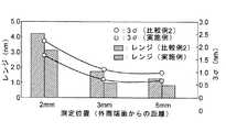
【表1】
ウエハWに形成されたレジスト膜の膜厚測定は、ウエハWの外周端面から3mm内側の円周上の点を最外周測定点とし、この円周内の直径上の複数箇所で行った。表1はその測定結果のレンジおよび3σの値を示している。ここで、「レンジ」は、測定した膜厚値の最大値と最小値の差を示しており、また、膜厚の最大値は最外周(つまり、ウエハWの外周端面から3mm内側の円周上)の膜厚の値であることから、このレンジの値が小さいということは、レジスト膜の外周部の跳ね上がりが小さいということを示している。また、「3σ」は膜厚分布の標準偏差であり、この値が小さいことはレジスト膜の厚さ均一性に優れていることを示している。
【0055】
表1に示されるように、比較例1よりも比較例2の場合でレンジおよび3σの値は小さく、さらに実施例の場合に、レンジおよび3σの値が最も小さくなっていることが分かる。比較例1および比較例2では、実施例と比較して雰囲気採取口がウエハWの端面に近い位置にあるために、ウエハWの周縁部では排気気流の影響によってレジスト膜が乾燥し易くなり、これによってレジスト膜厚が厚くなり易いと考えられる。なお、比較例1は比較例2と比べると、鉛直方向に流れる気流がウエハWの周縁部にあたってレジスト膜を乾燥させるために、レジスト膜が厚くなるものと考えられる。
【0056】
図7は、比較例2と実施例について、ウエハWの外周端面から2mm、3mm、5mmの位置でのレンジと3σの値を示したグラフである。この図7から、実施例では、ウエハWの周縁部におけるレジスト膜厚の跳ね上がりが抑制されていることがわかる。さらに、図8は、スピンチャック41の回転数を800rpmとした場合のウエハWの径方向におけるレジスト膜厚の変化を示しており、実施例の場合に、ウエハWの周縁部におけるレジスト膜の跳ね上がりが抑制されていることがわかる。これら図7および図8からも、実施例の処理カップを用いることによって、ウエハW全体で膜厚が均一なレジスト膜を形成することができることがわかる。なお、図8に示されるように、実施例の場合には比較例1・2と比較すると全体的に膜厚が10nm薄くなっているが、これは回転数や回転時間を調節することによって、所定の膜厚に絞り込むことができる。
【0057】
図9は、スピンチャック41の回転数を一定として、排気口72における排気圧を変化させた場合の膜厚を、ウエハWの外周端面から3mm内側の円周上の点を最外周測定点としてこの円周内の直径上の複数箇所で測定した結果(レンジおよび3σ)を示している。排気口72における排気圧を変化させると、排気流路55と排液流路56における排気圧も変化するが、図9に示されるように、レジスト膜の厚さには、このような排気圧の影響は殆ど現れないことが確認された。このことは、レジスト膜の厚さを一定に維持しながら、確実にウエハWの周囲の雰囲気の排気を行うことができることを示している。
【0058】
以上、本発明の実施の形態について説明してきたが、本発明はこのような形態に限定されるものではない。例えば、保持アーム78が昇降自在であるから、レジスト塗布処理ユニット(COT)においては、スピンチャック41を昇降させることなくウエハWを保持する位置を一定に固定し、スピンチャック41と保持アーム78との間でウエハWの受け渡しをする際に、処理カップ50をウエハWの受け渡しの障害とならないように昇降させてもよい。基板は半導体ウエハに限定されず、FPD(フラットパネルディスプレイ)用のガラス基板であってもよい。また、塗布液はレジスト膜に限定されるものではなく、例えば、層間絶縁膜をスピンコート法によって形成するために使用される薬液であってもよい。
【0059】
【発明の効果】
上述の通り、本発明の塗布処理装置によれば、基板の周囲の雰囲気を排気するに際して、排気される気流の基板の周縁部への影響を小さくすることができるために、基板周縁部での膜厚の上昇を抑制して、基板全体で厚さ分布の均一な塗布膜を形成することができる。これにより信頼性に優れる製品を製造することができ、また、製造歩留まりを向上させることができる。
【図面の簡単な説明】
【図1】レジスト塗布・現像処理システムの概略構造を示す平面図。
【図2】レジスト塗布・現像処理システムの概略構造を示す正面図。
【図3】レジスト塗布・現像処理システムの概略構造を示す背面図。
【図4】レジスト塗布処理ユニットの概略構造を示す断面図。
【図5】図4に示す領域Aの拡大図。
【図6】比較例1、比較例2および実施例に係るそれぞれの処理カップの概略構造を示す説明図。
【図7】比較例1と実施例の処理カップを用いて成膜されたレジスト膜のレンジと3σの値を示すグラフ。
【図8】比較例1、比較例2および実施例の処理カップを用いて成膜された各レジスト膜のウエハの径方向における膜厚変化を示すグラフ。
【図9】実施例の処理カップを用いて排気圧を変化させた場合のウエハの径方向におけるレジスト膜厚の変化を示すグラフ。
【符号の説明】
41;スピンチャック
50;処理カップ
51;第1カップ
52;気流制御部材
53;第2カップ
55;排気流路
55a;雰囲気採取口
56;排液流路
56a;レジスト液採取口
57;排気/排液流路
62a;上リング部材
62b;下リング部材
COT;レジスト塗布処理ユニット
W;半導体ウエハ[0001]
[Technical field to which the invention belongs]
The present invention relates to a coating processing apparatus that forms a coating film on a substrate to be processed.
[0002]
[Prior art]
For example, in a semiconductor device manufacturing process, a predetermined circuit pattern is formed on a semiconductor wafer by using a so-called photolithography technique. In this photolithography process, a circuit pattern is formed by forming a resist film on the wafer, exposing the resist film in a predetermined pattern, and developing the exposed wafer.
[0003]
Here, as a method of forming a resist film on the wafer, a predetermined amount of resist solution is supplied to the central portion of the wafer held in a substantially horizontal posture, and then the resist solution is spread over the entire wafer by rotating the wafer at a high speed. The so-called spin coating method is widely used. As an apparatus for forming a film by such a spin coating method, for example, Japanese Patent Laid-Open No. 2001-189266 (Patent Document 1) is arranged so as to surround a wafer and forcibly exhausts air from the bottom. A coating cup for forcibly evacuating the atmosphere around the wafer, and an airflow control plate that is disposed so as to surround the outer periphery of the wafer inside the processing cup and controls an airflow generated in the vicinity of the wafer. An apparatus is disclosed.
[0004]
[Patent Document 1]
Japanese Patent Laid-Open No. 2001-189266 (page 3 to page 4, FIG. 1)
[0005]
[Problems to be solved by the invention]
However, in such a coating processing apparatus, since the atmosphere sampling port of the exhaust channel is located in the vicinity of the end surface of the wafer, the resist at the peripheral edge of the wafer is caused by the air current flowing into the exhaust channel of the wafer end surface. The liquid dries faster. In this case, since the resist solution flowing from the center of the wafer toward the periphery easily deposits at the periphery of the wafer, the thickness of the resist film is thicker at the periphery of the wafer than at the center. In recent years, the thickness of resist films to be formed has been reduced as circuit patterns have become finer and more highly integrated, and a slight unevenness in resist film thickness has had a major impact on manufacturing yield and product quality. Is starting to give.
[0006]
The present invention has been made in view of such circumstances, and an object of the present invention is to provide a coating processing apparatus capable of forming a coating film having excellent thickness uniformity.
[0007]
[Means for Solving the Problems]
That is, according to the first aspect of the present invention, a predetermined coating solution is supplied to a substrate to be processed and the substrate is rotated to expand the coating solution and form a coating film having a uniform thickness distribution. A coating processing apparatus forOn the surface A holding means for holding the substrate to be processed to which the coating liquid is supplied in a substantially horizontal posture, a rotating means for rotating the substrate to be processed in a horizontal plane, and the holding means are housed and exhausted from the bottom to discharge the substrate. A processing container for exhausting the atmosphere around the processing substrate, and the processing container includes:A side wall portion comprising a cylindrical vertical wall and an inclined wall that is connected to the upper end of the vertical wall and tilts inward and upward, and the side wall portion is disposed so as to surround the outside of the substrate to be processed. One cup, an upper ring portion that is close to the substrate to be processed and surrounds the substrate to be processed inside the first cup, and protrudes upward with a substantially triangular section and protrudes downward with a substantially triangular section An air flow control member having a substantially square cross section formed of a lower ring portion, and an exhaust passage for substantially exhausting the atmosphere around the substrate to be processed is provided on the side wall portion of the first cup and the air flow Formed between the control member and An atmosphere collection port in the exhaust channel is located on an outer upper portion of the substrate to be processed, and the atmosphere collection port is formed between an upper end portion of the first cup and the apex of the airflow control member. An application processing apparatus is provided.
[0009]
According to such a coating processing apparatus, when the atmosphere around the substrate is exhausted, the influence of the exhausted airflow on the peripheral portion of the substrate can be reduced. Thereby, a coating film having a uniform thickness distribution can be formed on the entire substrate.
[0010]
DETAILED DESCRIPTION OF THE INVENTION
Hereinafter, embodiments of the present invention will be described with reference to the drawings. Here, a resist coating / development processing apparatus that includes a resist coating processing unit that forms a coating film by coating a resist film on a semiconductor wafer and that performs a series of processes from the formation of the resist film to the development process is taken as an example. To do.
[0011]
1 is a schematic plan view showing a resist coating / developing
[0012]
The
[0013]
A plurality (four in the figure) of
[0014]
The
[0015]
The
[0016]
As shown in FIG. 3, the main
[0017]
As shown in FIG. 1, in the resist coating /
[0018]
First processing unit G1 Then, in the coater cup (CP), a resist coating processing unit (COT) which is two spinner type processing units for performing predetermined processing by placing the wafer W on a spin chuck (not shown) and a development processing unit for developing a resist pattern. (DEV) are stacked in two steps from the bottom. Second processing unit G2 Similarly, a resist application processing unit (COT) and a development processing unit (DEV) are stacked in two stages from the bottom as two spinner type processing units. The structure of the resist coating unit (COT) will be described in detail later.
[0019]
Third processing unit G3 In FIG. 3, oven-type processing units that perform predetermined processing by placing the wafer W on the mounting table SP are stacked in multiple stages. That is, an adhesion unit (AD) that performs so-called hydrophobic treatment for improving the fixability of the resist, an alignment unit (ALIM) that performs alignment, an extension unit (EXT) that carries in and out the wafer W, and cooling processing A cooling plate unit (COL) to be performed, and four hot plate units (HP) for performing heat treatment on the wafer W coated with the resist solution or the wafer W after the exposure processing are stacked in eight stages in order from the bottom. A cooling plate unit (COL) may be provided instead of the alignment unit (ALIM), and the cooling plate unit (COL) may have an alignment function.
[0020]
Fourth processing unit G4 The oven-type processing units are stacked in multiple stages. That is, a cooling plate unit (COL), an extension / cooling plate unit (EXTCOL), which is a wafer loading / unloading section provided with a cooling plate, an extension unit (EXT), a cooling plate unit (COL), and four hot plate units (HP) ) Are stacked in 8 steps from the bottom.
[0021]
On the back side of the main
[0022]
The
[0023]
The
[0024]
In the resist coating / developing
[0025]
The wafer W is transferred from the extension unit (EXT) to the
[0026]
The wafer W that has been processed in the adhesion processing unit (AD) and has been cooled by the cooling plate unit (COL), or the wafer W that has not been processed in the adhesion processing unit (AD), is continuously processed by the
[0027]
The cooled wafer W is transferred to the third processing unit G.3 After being transferred to the alignment unit (ALIM) and aligned there, the fourth processing unit G4 Are transferred to the
[0028]
The wafer W is subjected to peripheral exposure by the
[0029]
The exposed wafer W is returned to the
[0030]
Thereafter, the wafer W is transferred to a development processing unit (DEV) where the exposure pattern is developed. After the development, the wafer W is transferred to the third processing unit G.3 To the hot plate unit (HP), where post-baking is performed. The wafer W having undergone such a series of processing is transferred to the third processing unit G.3 Is returned to the
[0031]
Next, the resist coating unit (COT) will be described in detail. 4 is a cross-sectional view showing a schematic structure of a resist coating unit (COT), and FIG. 5 is an enlarged view of a region A in FIG. The resist coating unit (COT) accommodates the
[0032]
A resist
[0033]
The
[0034]
The
[0035]
The
[0036]
In the
[0037]
An exhaust device (not shown) is provided downstream of the
[0038]
As shown in FIG. 5, an exhaust intake port (hereinafter referred to as “atmosphere sampling port”) 55 a in the
[0039]
Since the
[0040]
When the airflow flows into the
[0041]
In order to effectively obtain such an effect, preferably, the resist solution shaken off from the wafer W when the
[0042]
The base angle θ inside the
[0043]
The base angle θ outside the
[0044]
The inner base angle (θ of the
[0045]
Width β of exhaust /
[0046]
In addition, when the exhaust airflow flows backward in the
[0047]
Processing of the wafer W in the resist coating unit (COT) having the above-described configuration is performed by the following steps. First, the holding
[0048]
The resist
[0049]
When the
[0050]
A part of the resist solution spun off from the wafer W may adhere to the inner slope of the
[0051]
After stopping the rotation of the
[0052]
Table 1 and FIGS. 7 and 8 show the results of film thickness distribution and the like obtained by forming the resist film on the wafer W by using the various processing cups shown in FIG. Show. 6 (a) to 6 (c) show portions located outside the wafer W as in FIG. 5, and the other portions are common. The processing cup (Comparative Example 1) shown in FIG. 6A schematically shows the
[0053]
[Table 1]
The film thickness of the resist film formed on the wafer W was measured at a plurality of points on the diameter within the circumference with points on the circumference 3 mm inside from the outer peripheral end face of the wafer W being the outermost circumference measurement points. Table 1 shows the measurement results. Range and 3σ values are shown. Where "range" is, It was measuredFilm thickness The difference between the maximum and minimum values,Also, the film thickness Maximum value is outermost circumference(That is, on the circumference 3 mm inside from the outer peripheral end surface of the wafer W) ofFilm thickness Since this value is a value, a small value in this range indicates that the jumping of the outer peripheral portion of the resist film is small. Further, “3σ” is a standard deviation of the film thickness distribution, and a small value indicates excellent thickness uniformity of the resist film.
[0055]
As shown in Table 1, the range and 3σ values are smaller in Comparative Example 2 than in Comparative Example 1, and the range and 3σ values are smallest in the Example. In Comparative Example 1 and Comparative Example 2, since the atmosphere sampling port is located closer to the end face of the wafer W than in the example, the resist film is easily dried by the influence of the exhaust airflow at the peripheral edge of the wafer W. As a result, it is considered that the resist film thickness tends to increase. Compared to Comparative Example 2, it is considered that Comparative Example 1 is thicker because the airflow flowing in the vertical direction dries the resist film at the periphery of the wafer W.
[0056]
FIG. 7 is a graph showing ranges and 3σ values at positions of 2 mm, 3 mm, and 5 mm from the outer peripheral end surface of the wafer W in Comparative Example 2 and the Example. From FIG. 7, it can be seen that in the example, the jumping of the resist film thickness at the peripheral edge of the wafer W is suppressed. Further, FIG. 8 shows changes in the resist film thickness in the radial direction of the wafer W when the rotation speed of the
[0057]
FIG. 9 shows the case where the exhaust pressure at the
[0058]
As mentioned above, although embodiment of this invention has been described, this invention is not limited to such a form. For example, since the holding
[0059]
【The invention's effect】
As described above, according to the coating processing apparatus of the present invention, when the atmosphere around the substrate is exhausted, the influence of the exhausted airflow on the peripheral portion of the substrate can be reduced. An increase in film thickness can be suppressed, and a coating film having a uniform thickness distribution can be formed over the entire substrate. As a result, a product with excellent reliability can be manufactured, and the manufacturing yield can be improved.
[Brief description of the drawings]
FIG. 1 is a plan view showing a schematic structure of a resist coating / development processing system.
FIG. 2 is a front view showing a schematic structure of a resist coating / development processing system.
FIG. 3 is a rear view showing a schematic structure of a resist coating / development processing system.
FIG. 4 is a sectional view showing a schematic structure of a resist coating unit.
FIG. 5 is an enlarged view of a region A shown in FIG.
FIG. 6 is an explanatory diagram showing a schematic structure of each processing cup according to Comparative Example 1, Comparative Example 2, and Example.
FIG. 7 is a graph showing a range and a 3σ value of a resist film formed using the processing cups of Comparative Example 1 and Example.
FIG. 8 is a graph showing changes in the film thickness in the radial direction of each resist film formed using the processing cups of Comparative Example 1, Comparative Example 2, and Example;
FIG. 9 is a graph showing changes in the resist film thickness in the radial direction of the wafer when the exhaust pressure is changed using the processing cup of the example.
[Explanation of symbols]
41; Spin chuck
50; Processing cup
51; 1st cup
52; Airflow control member
53; second cup
55; exhaust passage
55a; atmosphere collection port
56; drainage channel
56a: Resist liquid sampling port
57; exhaust / drainage flow path
62a; upper ring member
62b; lower ring member
COT: Resist coating unit
W: Semiconductor wafer
Claims (10)
Translated fromJapanese表面に塗布液が供給される被処理基板を略水平姿勢で保持する保持手段と、
前記被処理基板を水平面内で回転させる回転手段と、
前記保持手段を収容し、底部から排気を行うことによって前記被処理基板の周囲の雰囲気を排気する処理容器と、
を具備し、
前記処理容器は、
筒状の鉛直壁および前記鉛直壁の上端に連設されて内側上方に傾倒した傾斜壁とからなる側壁部を有し、前記側壁部が前記被処理基板の外側を囲うように配置された第1カップと、
前記第1カップの内側において前記被処理基板に近接して前記被処理基板を囲うように配置され、断面略三角形で上に凸である上リング部および断面略三角形で下に凸である下リング部から構成された断面略四角形の気流制御部材と、
を有し、
実質的に前記被処理基板の周囲の雰囲気を排気する排気流路が前記第1カップの側壁部と前記気流制御部材との間に形成され、
前記排気流路における雰囲気採取口が前記被処理基板の外方上部に位置し、前記雰囲気採取口が、前記第1カップの上端部と前記気流制御部材の頂点との間に形成されていることを特徴とする塗布処理装置。A coating processing apparatus for supplying a predetermined coating solution to a substrate to be processed and rotating the substrate to be processed to expand the coating solution to form a coating film having a uniform thickness distribution,
Holding means for holding the substrate to be treated, to which the coating liquid is supplied on the surface, in a substantially horizontal posture;
Rotating means for rotating the substrate to be processed in a horizontal plane;
A processing container containing the holding means and exhausting the atmosphere around the substrate to be processed by exhausting from the bottom;
Comprising
The processing container is
A side wall portion comprising a cylindrical vertical wall and an inclined wall that is connected to the upper end of the vertical wall and tilts inward and upward, and the side wall portion is disposed so as to surround the outside of the substrate to be processed. 1 cup,
An upper ring portion that is disposed in the first cup so as to surround the substrate to be processed in the vicinity of the substrate to be processed, and has a substantially triangular cross section and is convex upward, and a lower ring that is substantially triangular in cross section and is convex downward An air flow control member having a substantially rectangular cross section composed of a portion;
Have
An exhaust passage that substantially exhausts the atmosphere around the substrate to be processed is formed between the side wall portion of the first cup and the airflow control member,
An atmosphere collection port in the exhaust channel is located on an outer upper portion of the substrate to be processed, and the atmosphere collection port is formed between an upper end portion of the first cup and the apex of the airflow control member. The coating processing apparatus characterized by this.
実質的に前記被処理基板から振り切られる塗布液を下方に向けて排出する排液流路が、前記気流制御部材と前記被処理基板との間隙が前記排液流路における排液採取口となって、前記気流制御部材と前記第2カップの傾斜壁との間に形成されていることを特徴とする請求項1に記載の塗布処理装置。The processing container further includes a second cup provided with an inclined wall that extends obliquely downward from the lower side of the substrate to be processed.
The drainage flow path for discharging downward the coating liquid that is substantially shaken off from the substrate to be processed is a drainage sampling port in the drainage flow path. The coating apparatus according toclaim 1 , wherein the coating apparatus is formed between the airflow control member and the inclined wall of the second cup.
前記排気流路の下流と前記排液流路の下流は、前記第1カップの側壁部と前記第2カップの側壁部との間に形成される間隙部で合流し、前記処理容器の底部から排気および排液が行われることを特徴とする請求項2に記載の塗布処理装置。The second cup further has a cylindrical side wall portion communicating with the lower end of the inclined wall of the second cup,
The downstream of the exhaust flow channel and the downstream of the drainage flow channel merge at a gap formed between the side wall of the first cup and the side wall of the second cup, and from the bottom of the processing vessel3. The coating treatment apparatus according toclaim 2 , wherein exhaust and drainage are performed.
Priority Applications (8)
| Application Number | Priority Date | Filing Date | Title |
|---|---|---|---|
| JP2002376233AJP4318913B2 (en) | 2002-12-26 | 2002-12-26 | Application processing equipment |
| PCT/JP2003/016154WO2004059709A1 (en) | 2002-12-26 | 2003-12-17 | Coating device and coating film forming method |
| EP03780822AEP1577930A4 (en) | 2002-12-26 | 2003-12-17 | Coating device and coating film forming method |
| US10/538,727US7575634B2 (en) | 2002-12-26 | 2003-12-17 | Coating device and coating film forming method |
| CNB2003801075768ACN100380584C (en) | 2002-12-26 | 2003-12-17 | Coating device and coating film forming method |
| KR1020057011969AKR100954901B1 (en) | 2002-12-26 | 2003-12-17 | Coating treatment apparatus and coating film forming method |
| AU2003289383AAU2003289383A1 (en) | 2002-12-26 | 2003-12-17 | Coating device and coating film forming method |
| US12/491,424US7790227B2 (en) | 2002-12-26 | 2009-06-25 | Coating process apparatus and coating film forming method |
Applications Claiming Priority (1)
| Application Number | Priority Date | Filing Date | Title |
|---|---|---|---|
| JP2002376233AJP4318913B2 (en) | 2002-12-26 | 2002-12-26 | Application processing equipment |
Publications (3)
| Publication Number | Publication Date |
|---|---|
| JP2004207573A JP2004207573A (en) | 2004-07-22 |
| JP2004207573A5 JP2004207573A5 (en) | 2005-06-16 |
| JP4318913B2true JP4318913B2 (en) | 2009-08-26 |
Family
ID=32677357
Family Applications (1)
| Application Number | Title | Priority Date | Filing Date |
|---|---|---|---|
| JP2002376233AExpired - Fee RelatedJP4318913B2 (en) | 2002-12-26 | 2002-12-26 | Application processing equipment |
Country Status (7)
| Country | Link |
|---|---|
| US (2) | US7575634B2 (en) |
| EP (1) | EP1577930A4 (en) |
| JP (1) | JP4318913B2 (en) |
| KR (1) | KR100954901B1 (en) |
| CN (1) | CN100380584C (en) |
| AU (1) | AU2003289383A1 (en) |
| WO (1) | WO2004059709A1 (en) |
Cited By (1)
| Publication number | Priority date | Publication date | Assignee | Title |
|---|---|---|---|---|
| US10811287B2 (en) | 2017-11-17 | 2020-10-20 | Samsung Electronics Co., Ltd. | Spin coater and substrate treating apparatus having the same |
Families Citing this family (36)
| Publication number | Priority date | Publication date | Assignee | Title |
|---|---|---|---|---|
| JP4642543B2 (en)* | 2005-05-09 | 2011-03-02 | 東京エレクトロン株式会社 | Edge exposure apparatus, coating and developing apparatus, and edge exposure method |
| JP4796902B2 (en)* | 2005-07-11 | 2011-10-19 | 芝浦メカトロニクス株式会社 | Substrate spin processing equipment |
| JP4519035B2 (en) | 2005-08-30 | 2010-08-04 | 東京エレクトロン株式会社 | Coating film forming device |
| KR100689664B1 (en)* | 2005-09-07 | 2007-03-08 | 삼성전자주식회사 | Wafer cleaning equipment |
| US7762887B1 (en) | 2006-12-04 | 2010-07-27 | G&G Technologies LLC | Systems and methods for electronically managing games |
| CN101354534B (en)* | 2007-07-27 | 2011-07-06 | 中芯国际集成电路制造(上海)有限公司 | Method for coating photoresist and method for forming photolithography pattern |
| US8999106B2 (en) | 2007-12-19 | 2015-04-07 | Applied Materials, Inc. | Apparatus and method for controlling edge performance in an inductively coupled plasma chamber |
| JP5084639B2 (en)* | 2008-06-30 | 2012-11-28 | 芝浦メカトロニクス株式会社 | Spin processing device |
| JP5508709B2 (en)* | 2008-12-22 | 2014-06-04 | 株式会社Sokudo | Coating processing apparatus and substrate processing apparatus |
| JP2010287686A (en)* | 2009-06-10 | 2010-12-24 | Tokyo Electron Ltd | Coating/developing device, and method for cleaning back of substrate |
| KR20110106178A (en)* | 2010-03-22 | 2011-09-28 | 삼성전자주식회사 | Substrate Processing Apparatus and Method |
| KR20110127055A (en)* | 2010-05-18 | 2011-11-24 | 주식회사 에스앤에스텍 | Method for manufacturing resist film forming apparatus, photomask blank and photomask blank |
| JP5242635B2 (en)* | 2010-06-29 | 2013-07-24 | 東京エレクトロン株式会社 | Coating method and coating apparatus |
| JP2012019025A (en)* | 2010-07-07 | 2012-01-26 | Tokyo Electron Ltd | Liquid processing unit |
| DE202010015018U1 (en)* | 2010-11-07 | 2011-04-14 | Bohnet, Hans | Arrangement for producing structured substrates |
| CN102319656B (en)* | 2011-09-21 | 2013-06-12 | 上海先进半导体制造股份有限公司 | HMDS automatic supply system and automatic supply method thereof |
| CN102707572A (en)* | 2012-06-06 | 2012-10-03 | 长春理工大学 | Device and method for scanning and spraying photoresist on convex spherical surface |
| JP6093569B2 (en)* | 2012-12-28 | 2017-03-08 | 株式会社荏原製作所 | Substrate cleaning device |
| JP6281161B2 (en)* | 2013-09-27 | 2018-02-21 | 東京エレクトロン株式会社 | Liquid processing equipment |
| US9817315B2 (en)* | 2014-03-13 | 2017-11-14 | Taiwan Semiconductor Manufacturing Co., Ltd. | System and method for supplying and dispensing bubble-free photolithography chemical solutions |
| JP6461617B2 (en)* | 2015-01-20 | 2019-01-30 | 株式会社Screenホールディングス | Substrate processing equipment |
| DE102015104735A1 (en)* | 2015-03-27 | 2016-09-29 | Obducat Ab | Turntable for receiving a substrate for a coating device |
| WO2016179818A1 (en)* | 2015-05-14 | 2016-11-17 | Acm Research (Shanghai) Inc. | Apparatus for substrate bevel and backside protection |
| KR102542886B1 (en)* | 2016-04-25 | 2023-06-12 | 동우 화인켐 주식회사 | Coating Jig and Coating Method Using the Same |
| JP6925213B2 (en)* | 2017-09-22 | 2021-08-25 | 東京エレクトロン株式会社 | Heat treatment equipment and heat treatment method |
| KR102353775B1 (en)* | 2019-11-27 | 2022-01-20 | 세메스 주식회사 | Substrate processing apparatus |
| US12198944B2 (en) | 2020-11-11 | 2025-01-14 | Applied Materials, Inc. | Substrate handling in a modular polishing system with single substrate cleaning chambers |
| KR102634281B1 (en) | 2020-12-21 | 2024-02-07 | 세메스 주식회사 | Apparatus for treating a substrate |
| KR102677969B1 (en)* | 2020-12-30 | 2024-06-26 | 세메스 주식회사 | Nozzel standby port, apparatus for treating substrate including the same and method for treating substrate using the same |
| KR102853348B1 (en)* | 2021-01-27 | 2025-08-29 | 삼성전자주식회사 | Apparatus of processing substrate |
| JP7628434B2 (en)* | 2021-02-15 | 2025-02-10 | 株式会社Screenホールディングス | Substrate processing apparatus and method for processing cylindrical guard |
| CN113655688A (en)* | 2021-09-08 | 2021-11-16 | 深圳市龙图光电有限公司 | Mask manufacturing device |
| WO2023079872A1 (en)* | 2021-11-04 | 2023-05-11 | 東京エレクトロン株式会社 | Substrate processing apparatus and substrate processing method |
| US20230229085A1 (en)* | 2022-01-19 | 2023-07-20 | Taiwan Semiconductor Manufacturing Company | Device and method to promote thickness uniformity in spin-coating |
| JP2023157122A (en)* | 2022-04-14 | 2023-10-26 | 東京エレクトロン株式会社 | Cup and substrate processing equipment |
| CN117198938B (en)* | 2023-09-15 | 2025-08-19 | 华海清科股份有限公司 | Wafer post-processing device |
Family Cites Families (99)
| Publication number | Priority date | Publication date | Assignee | Title |
|---|---|---|---|---|
| JPS6439023A (en)* | 1987-08-05 | 1989-02-09 | Seiko Epson Corp | Structure for preventing splashing in rotating body |
| JPH0421467Y2 (en) | 1987-09-02 | 1992-05-15 | ||
| JP2907877B2 (en)* | 1989-07-31 | 1999-06-21 | 株式会社日立製作所 | Coating device and coating method |
| US5297031A (en)* | 1990-03-06 | 1994-03-22 | Chicago Board Of Trade | Method and apparatus for order management by market brokers |
| CA2044931C (en)* | 1990-06-19 | 2000-08-01 | Hajime Kamata | Multiwindow display control method and apparatus |
| JPH0699125A (en)* | 1992-09-24 | 1994-04-12 | Mitsubishi Plastics Ind Ltd | Spin coater and optical disc manufacturing method |
| JPH0910658A (en)* | 1995-06-27 | 1997-01-14 | Hitachi Ltd | Coating method and coating device |
| JPH0917722A (en) | 1995-06-27 | 1997-01-17 | Hitachi Ltd | Coating device |
| JPH0945611A (en)* | 1995-07-27 | 1997-02-14 | Dainippon Screen Mfg Co Ltd | Spin coater of substrate |
| US6209004B1 (en)* | 1995-09-01 | 2001-03-27 | Taylor Microtechnology Inc. | Method and system for generating and distributing document sets using a relational database |
| JP3589518B2 (en) | 1995-11-30 | 2004-11-17 | 大日本スクリーン製造株式会社 | Substrate processing equipment |
| US6519574B1 (en)* | 1995-12-12 | 2003-02-11 | Reuters Limited | Electronic trading system featuring arbitrage and third-party credit opportunities |
| NZ332244A (en)* | 1996-04-12 | 2000-10-27 | Citibank Na | Synthetic currency (inside money) transaction agent and network |
| US6014643A (en)* | 1996-06-28 | 2000-01-11 | Minton; Vernon F. | Interactive securities trading system |
| US6029146A (en)* | 1996-08-21 | 2000-02-22 | Crossmar, Inc. | Method and apparatus for trading securities electronically |
| US6016483A (en)* | 1996-09-20 | 2000-01-18 | Optimark Technologies, Inc. | Method and apparatus for automated opening of options exchange |
| US6850907B2 (en)* | 1996-12-13 | 2005-02-01 | Cantor Fitzgerald, L.P. | Automated price improvement protocol processor |
| US5873071A (en)* | 1997-05-15 | 1999-02-16 | Itg Inc. | Computer method and system for intermediated exchange of commodities |
| US20070061452A1 (en)* | 1997-05-23 | 2007-03-15 | The Thomson Corporation | Market data notification system |
| US6996540B1 (en)* | 1997-10-14 | 2006-02-07 | Blackbird Holdings, Inc. | Systems for switch auctions utilizing risk position portfolios of a plurality of traders |
| US6535917B1 (en)* | 1998-02-09 | 2003-03-18 | Reuters, Ltd. | Market data domain and enterprise system implemented by a master entitlement processor |
| US6343278B1 (en)* | 1998-09-04 | 2002-01-29 | Ebs Dealing Resources, Inc. | Combined order limit for a group of related transactions in an automated dealing system |
| US7020632B1 (en)* | 1999-01-11 | 2006-03-28 | Lawrence Kohls | Trading system for fixed-value contracts |
| US6513019B2 (en)* | 1999-02-16 | 2003-01-28 | Financial Technologies International, Inc. | Financial consolidation and communication platform |
| US6993504B1 (en)* | 1999-04-09 | 2006-01-31 | Trading Technologies International, Inc. | User interface for semi-fungible trading |
| US7212999B2 (en)* | 1999-04-09 | 2007-05-01 | Trading Technologies International, Inc. | User interface for an electronic trading system |
| US6505175B1 (en)* | 1999-10-06 | 2003-01-07 | Goldman, Sachs & Co. | Order centric tracking system |
| JP3599323B2 (en) | 1999-10-19 | 2004-12-08 | 東京エレクトロン株式会社 | Substrate processing equipment |
| US6527860B1 (en)* | 1999-10-19 | 2003-03-04 | Tokyo Electron Limited | Substrate processing apparatus |
| SG166005A1 (en)* | 2000-02-01 | 2010-11-29 | Tokyo Electron Ltd | Substrate processing apparatus and substrate processing method |
| JP2002110517A (en) | 2000-09-28 | 2002-04-12 | Toshiba Corp | Liquid removal method |
| TWI228755B (en)* | 2000-02-17 | 2005-03-01 | Toshiba Corp | Chemical liquid processing apparatus and the method thereof |
| US20020026401A1 (en)* | 2000-02-21 | 2002-02-28 | Hueler Kelli Hustad | System and method for facilitating electronic bidding between buyers and sellers in financial industries |
| US6938011B1 (en)* | 2000-03-02 | 2005-08-30 | Trading Technologies International, Inc. | Click based trading with market depth display |
| US7127424B2 (en)* | 2000-03-02 | 2006-10-24 | Trading Technologies International, Inc. | Click based trading with intuitive grid display of market depth and price consolidation |
| US7389268B1 (en)* | 2000-03-02 | 2008-06-17 | Trading Technologies International, Inc. | Trading tools for electronic trading |
| US6772132B1 (en)* | 2000-03-02 | 2004-08-03 | Trading Technologies International, Inc. | Click based trading with intuitive grid display of market depth |
| US7003486B1 (en)* | 2000-04-17 | 2006-02-21 | Neha Net Corp. | Net-value creation and allocation in an electronic trading system |
| US6868400B1 (en)* | 2000-05-24 | 2005-03-15 | Nehanet Corp. | Spread-maximizing travel-services trading system using buyer- and seller-specified multi-attribute values |
| US7437325B2 (en)* | 2002-03-05 | 2008-10-14 | Pablo Llc | System and method for performing automatic spread trading |
| WO2002003302A1 (en)* | 2000-06-30 | 2002-01-10 | Enron Net Works Llc | Buying and selling goods and services using automated method and apparatus |
| US7177833B1 (en)* | 2000-07-18 | 2007-02-13 | Edge Capture, Llc | Automated trading system in an electronic trading exchange |
| NO312427B1 (en)* | 2000-08-04 | 2002-05-06 | Usertrade As | Electronic trading system |
| AUPQ950400A0 (en)* | 2000-08-17 | 2000-09-07 | Peruch, Stephen Sebastian | Computer implemented system and method of transforming a source file into transformed file using a set of trigger instructions |
| GB2386725A (en)* | 2000-10-30 | 2003-09-24 | Liquidity Direct Technology | Network and method for trading derivatives |
| US7184984B2 (en)* | 2000-11-17 | 2007-02-27 | Valaquenta Intellectual Properties Limited | Global electronic trading system |
| GB2376319A (en)* | 2001-06-05 | 2002-12-11 | Security & Standards Ltd | Validation System |
| US7702563B2 (en)* | 2001-06-11 | 2010-04-20 | Otc Online Partners | Integrated electronic exchange of structured contracts with dynamic risk-based transaction permissioning |
| US20030009419A1 (en)* | 2001-06-11 | 2003-01-09 | Chavez R. Martin | Risk management system and trade engine with automatic trade feed and market data feed |
| CA2403300A1 (en)* | 2002-09-12 | 2004-03-12 | Pranil Ram | A method of buying or selling items and a user interface to facilitate the same |
| US7650305B1 (en)* | 2001-10-03 | 2010-01-19 | I2 Technologies Us, Inc. | Displaying market data |
| US7672895B2 (en)* | 2002-02-19 | 2010-03-02 | Trading Technologies International, Inc. | System and method for simulating an electronic trading environment |
| US8666869B2 (en)* | 2002-08-06 | 2014-03-04 | Redi Tech, Llc | Systems for electronic trading |
| AU2003301476A1 (en)* | 2002-10-15 | 2004-05-04 | Liquidity Direct Technology, Llc | Network and method for trading derivatives by providing enhanced rfq visibility |
| US7426490B1 (en)* | 2002-10-31 | 2008-09-16 | Trading Technologies International, Inc. | System and method for automated order entry on short queues |
| US7418422B2 (en)* | 2002-11-13 | 2008-08-26 | Trading Technologies International, Inc. | Method, apparatus and interface for trading multiple tradeable objects |
| US7523064B2 (en)* | 2002-11-13 | 2009-04-21 | Trading Technologies International, Inc. | System and method for facilitating trading of multiple tradeable objects in an electronic trading environment |
| US8041622B1 (en)* | 2002-11-26 | 2011-10-18 | Trading Technologies International Inc. | System and method for randomizing orders in an electronic trading environment |
| US7603303B1 (en)* | 2002-11-26 | 2009-10-13 | Trading Technologies International, Inc. | System and method for risk management |
| US7577602B2 (en)* | 2002-11-26 | 2009-08-18 | Trading Technologies International Inc. | Method and interface for consolidating price levels on a trading screen |
| US7769668B2 (en)* | 2002-12-09 | 2010-08-03 | Sam Balabon | System and method for facilitating trading of financial instruments |
| US7483854B2 (en)* | 2003-01-24 | 2009-01-27 | Liu Michael C | Method and system for intelligent automated security trading via the internet |
| US7512557B1 (en)* | 2003-06-30 | 2009-03-31 | Trading Technologies International, Inc. | System and method for timed order entry and modification |
| US7739182B2 (en)* | 2003-07-03 | 2010-06-15 | Makor Issues And Rights Ltd. | Machine learning automatic order transmission system for sending self-optimized trading signals |
| US7756782B2 (en)* | 2003-07-28 | 2010-07-13 | Trading Technologies International, Inc. | System and method for improved electronic trading |
| US7624063B1 (en)* | 2003-09-30 | 2009-11-24 | Trading Technologies International, Inc. | System and method for improved distribution of market information |
| US7668767B1 (en)* | 2003-10-01 | 2010-02-23 | Trading Technologies International, Inc. | System and method for dynamic quantity orders in an electronic trading environment |
| US7765143B1 (en)* | 2003-11-04 | 2010-07-27 | Trading Technologies International, Inc. | System and method for event driven virtual workspace |
| US7647266B1 (en)* | 2004-03-24 | 2010-01-12 | Trading Technologies International, Inc. | System and method for holding and sending an order to a matching engine |
| US7218325B1 (en)* | 2004-03-31 | 2007-05-15 | Trading Technologies International, Inc. | Graphical display with integrated recent period zoom and historical period context data |
| US7890396B2 (en)* | 2005-06-07 | 2011-02-15 | Cfph, Llc | Enhanced system and method for managing financial market information |
| US8232962B2 (en)* | 2004-06-21 | 2012-07-31 | Trading Technologies International, Inc. | System and method for display management based on user attention inputs |
| US20100076906A1 (en)* | 2004-07-12 | 2010-03-25 | Rosenthal Collins Group, L.L.C. | Method and system for using quantitative analytics on a graphical user interface for electronic trading |
| US20060010066A1 (en)* | 2004-07-12 | 2006-01-12 | Rosenthal Collins Group, L.L.C. | Method and system for providing a graphical user interface for electronic trading |
| WO2006036942A2 (en)* | 2004-09-27 | 2006-04-06 | Citadel Investment Group, L.L.C. | Providing guaranteed, specified and/or predetermined execution prices in a guaranteed, specified and/or predetermined timeframe on the purchase or sale of listed options |
| US7542938B1 (en)* | 2004-12-28 | 2009-06-02 | Trading Technologies International, Inc. | System and method for quick quote configuration |
| US7487125B2 (en)* | 2005-01-14 | 2009-02-03 | Littlewood Margaret G | Method for providing aggregation of trading on multiple alternative trading systems |
| USD538817S1 (en)* | 2005-05-05 | 2007-03-20 | Noviello Joseph C | User interface for an electronic trading system for a computer screen |
| USD538818S1 (en)* | 2005-05-05 | 2007-03-20 | Noviello Joseph C | User interface for an electronic trading system for a computer screen |
| USD538815S1 (en)* | 2005-05-05 | 2007-03-20 | Noviello Joseph C | User interface for an electronic trading system for a computer screen |
| USD539297S1 (en)* | 2005-05-05 | 2007-03-27 | Noviello Joseph C | User interface for an electronic trading system for a computer screen |
| USD559259S1 (en)* | 2005-05-05 | 2008-01-08 | Espeed Inc. | User interface for an electronic trading system for a computer screen |
| USD559260S1 (en)* | 2005-05-05 | 2008-01-08 | Espeed Inc. | User interface for an electronic trading system for a computer screen |
| USD538816S1 (en)* | 2005-05-05 | 2007-03-20 | Noviello Joseph C | User interface for an electronic trading system for a computer screen |
| USD538295S1 (en)* | 2005-05-05 | 2007-03-13 | Noviello Joseph C | User interface for an electronic trading system for a computer screen |
| USD538294S1 (en)* | 2005-05-05 | 2007-03-13 | Noviello Joseph C | User interface for an electronic trading system for a computer screen |
| US20100076907A1 (en)* | 2005-05-31 | 2010-03-25 | Rosenthal Collins Group, Llc. | Method and system for automatically inputting, monitoring and trading risk- controlled spreads |
| US7711630B2 (en)* | 2005-06-06 | 2010-05-04 | Trading Technologies International. Inc. | System and method for trading multiple tradeable objects using a single trading interface |
| US7565318B2 (en)* | 2005-06-28 | 2009-07-21 | Trading Technologies International, Inc. | System and method for calculating and displaying volume to identify buying and selling in an electronic trading environment |
| US20070016509A1 (en)* | 2005-07-15 | 2007-01-18 | Vogel Robert P | Computerized transaction-based yield curve analytics |
| US7933828B2 (en)* | 2005-07-26 | 2011-04-26 | Cfph, Llc | System and method for displaying and/or analyzing a limit order book |
| US7624066B2 (en)* | 2005-08-10 | 2009-11-24 | Tradehelm, Inc. | Method and apparatus for electronic trading of financial instruments |
| US20070043647A1 (en)* | 2005-08-16 | 2007-02-22 | American Stock Exchange Llc | Electronic trading environment with price improvement |
| US7672896B2 (en)* | 2005-09-30 | 2010-03-02 | Trading Technologies International, Inc. | System and method for order placement in an electronic trading environment |
| WO2007095742A1 (en)* | 2006-02-27 | 2007-08-30 | Lange David H | System and method for determining and brokering fuel emission offsets |
| US20080059846A1 (en)* | 2006-08-31 | 2008-03-06 | Rosenthal Collins Group, L.L.C. | Fault tolerant electronic trading system and method |
| US20100010937A1 (en)* | 2008-04-30 | 2010-01-14 | Rosenthal Collins Group, L.L.C. | Method and system for providing risk assessment management and reporting for multi-market electronic trading |
| US7844726B2 (en)* | 2008-07-28 | 2010-11-30 | Trading Technologies International, Inc. | System and method for dynamically managing message flow |
| US20100036704A1 (en)* | 2008-08-05 | 2010-02-11 | International Business Machines Corporation | Method and system for allocating requirements in a service oriented architecture using software and hardware string representation |
- 2002
- 2002-12-26JPJP2002376233Apatent/JP4318913B2/ennot_activeExpired - Fee Related
- 2003
- 2003-12-17EPEP03780822Apatent/EP1577930A4/ennot_activeWithdrawn
- 2003-12-17AUAU2003289383Apatent/AU2003289383A1/ennot_activeAbandoned
- 2003-12-17CNCNB2003801075768Apatent/CN100380584C/ennot_activeExpired - Fee Related
- 2003-12-17USUS10/538,727patent/US7575634B2/ennot_activeExpired - Fee Related
- 2003-12-17WOPCT/JP2003/016154patent/WO2004059709A1/enactiveApplication Filing
- 2003-12-17KRKR1020057011969Apatent/KR100954901B1/ennot_activeExpired - Fee Related
- 2009
- 2009-06-25USUS12/491,424patent/US7790227B2/ennot_activeExpired - Fee Related
Cited By (1)
| Publication number | Priority date | Publication date | Assignee | Title |
|---|---|---|---|---|
| US10811287B2 (en) | 2017-11-17 | 2020-10-20 | Samsung Electronics Co., Ltd. | Spin coater and substrate treating apparatus having the same |
Also Published As
| Publication number | Publication date |
|---|---|
| US20060068093A1 (en) | 2006-03-30 |
| WO2004059709A1 (en) | 2004-07-15 |
| CN1732555A (en) | 2006-02-08 |
| US7790227B2 (en) | 2010-09-07 |
| CN100380584C (en) | 2008-04-09 |
| AU2003289383A1 (en) | 2004-07-22 |
| EP1577930A1 (en) | 2005-09-21 |
| KR100954901B1 (en) | 2010-04-27 |
| JP2004207573A (en) | 2004-07-22 |
| US20090258139A1 (en) | 2009-10-15 |
| KR20050086941A (en) | 2005-08-30 |
| US7575634B2 (en) | 2009-08-18 |
| EP1577930A4 (en) | 2010-01-06 |
Similar Documents
| Publication | Publication Date | Title |
|---|---|---|
| JP4318913B2 (en) | Application processing equipment | |
| JP5012651B2 (en) | Coating device, coating method, coating, developing device and storage medium | |
| JP3616748B2 (en) | Development processing method, development processing apparatus, and processing apparatus | |
| KR102410089B1 (en) | Liquid processing apparatus and liquid processing method | |
| JP3527426B2 (en) | Development processing method and development processing apparatus | |
| JP5072380B2 (en) | Substrate processing system | |
| JP3625752B2 (en) | Liquid processing equipment | |
| JP2003007669A (en) | Substrate processing apparatus | |
| CN108630529B (en) | Coating treatment device and cup body | |
| JP2003045788A (en) | Wafer processing method and apparatus | |
| JP3679695B2 (en) | Developing apparatus, substrate processing apparatus, and developing method | |
| JP2003218015A (en) | Substrate processing device | |
| KR102046872B1 (en) | Apparatus and Method for treating substrate | |
| JP3479602B2 (en) | Substrate processing apparatus and substrate processing method | |
| JP3909574B2 (en) | Resist coating device | |
| JP3485471B2 (en) | Processing device and processing method | |
| JP3634983B2 (en) | Heat treatment equipment | |
| JP3266817B2 (en) | Coating device and coating method | |
| JP3811359B2 (en) | Liquid processing equipment | |
| JP3352419B2 (en) | Coating film forming method and coating processing system | |
| JPH06216018A (en) | Coating device | |
| JP7158549B2 (en) | SUBSTRATE PROCESSING METHOD, SUBSTRATE PROCESSING SYSTEM AND COMPUTER-READABLE STORAGE MEDIUM | |
| WO2004036633A1 (en) | Liquid processing device | |
| JP2003086491A (en) | Treatment method of substrate, and forming method of coating film | |
| JP2001319919A (en) | Method and apparatus for manufacturing semiconductor device |
Legal Events
| Date | Code | Title | Description |
|---|---|---|---|
| A521 | Written amendment | Free format text:JAPANESE INTERMEDIATE CODE: A523 Effective date:20040916 | |
| A621 | Written request for application examination | Free format text:JAPANESE INTERMEDIATE CODE: A621 Effective date:20040916 | |
| A131 | Notification of reasons for refusal | Free format text:JAPANESE INTERMEDIATE CODE: A131 Effective date:20070731 | |
| A521 | Written amendment | Free format text:JAPANESE INTERMEDIATE CODE: A523 Effective date:20070927 | |
| A02 | Decision of refusal | Free format text:JAPANESE INTERMEDIATE CODE: A02 Effective date:20080930 | |
| A521 | Written amendment | Free format text:JAPANESE INTERMEDIATE CODE: A523 Effective date:20081027 | |
| A911 | Transfer of reconsideration by examiner before appeal (zenchi) | Free format text:JAPANESE INTERMEDIATE CODE: A911 Effective date:20081203 | |
| TRDD | Decision of grant or rejection written | ||
| A01 | Written decision to grant a patent or to grant a registration (utility model) | Free format text:JAPANESE INTERMEDIATE CODE: A01 Effective date:20090526 | |
| A01 | Written decision to grant a patent or to grant a registration (utility model) | Free format text:JAPANESE INTERMEDIATE CODE: A01 | |
| A61 | First payment of annual fees (during grant procedure) | Free format text:JAPANESE INTERMEDIATE CODE: A61 Effective date:20090527 | |
| FPAY | Renewal fee payment (event date is renewal date of database) | Free format text:PAYMENT UNTIL: 20120605 Year of fee payment:3 | |
| R150 | Certificate of patent or registration of utility model | Free format text:JAPANESE INTERMEDIATE CODE: R150 | |
| FPAY | Renewal fee payment (event date is renewal date of database) | Free format text:PAYMENT UNTIL: 20150605 Year of fee payment:6 | |
| R250 | Receipt of annual fees | Free format text:JAPANESE INTERMEDIATE CODE: R250 | |
| LAPS | Cancellation because of no payment of annual fees |