JP4310633B2 - High frequency switch - Google Patents
High frequency switchDownload PDFInfo
- Publication number
- JP4310633B2 JP4310633B2JP2003416693AJP2003416693AJP4310633B2JP 4310633 B2JP4310633 B2JP 4310633B2JP 2003416693 AJP2003416693 AJP 2003416693AJP 2003416693 AJP2003416693 AJP 2003416693AJP 4310633 B2JP4310633 B2JP 4310633B2
- Authority
- JP
- Japan
- Prior art keywords
- variable device
- frequency
- circuit
- variable
- waveguide
- Prior art date
- Legal status (The legal status is an assumption and is not a legal conclusion. Google has not performed a legal analysis and makes no representation as to the accuracy of the status listed.)
- Expired - Fee Related
Links
- 230000005540biological transmissionEffects0.000claimsdescription24
- 238000005513bias potentialMethods0.000claimsdescription3
- 239000010408filmSubstances0.000description17
- 239000000758substrateSubstances0.000description16
- 229910052751metalInorganic materials0.000description15
- 239000002184metalSubstances0.000description15
- PCHJSUWPFVWCPO-UHFFFAOYSA-NgoldChemical compound[Au]PCHJSUWPFVWCPO-UHFFFAOYSA-N0.000description14
- 229910052737goldInorganic materials0.000description13
- 239000010931goldSubstances0.000description13
- OMZSGWSJDCOLKM-UHFFFAOYSA-Ncopper(II) sulfideChemical compound[S-2].[Cu+2]OMZSGWSJDCOLKM-UHFFFAOYSA-N0.000description9
- 238000010586diagramMethods0.000description8
- RYGMFSIKBFXOCR-UHFFFAOYSA-NCopperChemical compound[Cu]RYGMFSIKBFXOCR-UHFFFAOYSA-N0.000description7
- 229910052802copperInorganic materials0.000description7
- 239000010949copperSubstances0.000description7
- 230000007423decreaseEffects0.000description5
- 230000000694effectsEffects0.000description5
- 239000011521glassSubstances0.000description5
- 238000002955isolationMethods0.000description5
- 229910001218Gallium arsenideInorganic materials0.000description3
- 229910052581Si3N4Inorganic materials0.000description3
- 238000004519manufacturing processMethods0.000description3
- 238000000034methodMethods0.000description3
- HQVNEWCFYHHQES-UHFFFAOYSA-Nsilicon nitrideChemical compoundN12[Si]34N5[Si]62N3[Si]51N64HQVNEWCFYHHQES-UHFFFAOYSA-N0.000description3
- 239000010409thin filmSubstances0.000description3
- 229910001111Fine metalInorganic materials0.000description2
- PXHVJJICTQNCMI-UHFFFAOYSA-NNickelChemical compound[Ni]PXHVJJICTQNCMI-UHFFFAOYSA-N0.000description2
- 229910052782aluminiumInorganic materials0.000description2
- XAGFODPZIPBFFR-UHFFFAOYSA-NaluminiumChemical compound[Al]XAGFODPZIPBFFR-UHFFFAOYSA-N0.000description2
- 150000004770chalcogenidesChemical class0.000description2
- 238000004891communicationMethods0.000description2
- 238000000151depositionMethods0.000description2
- 238000005516engineering processMethods0.000description2
- 239000010416ion conductorSubstances0.000description2
- -1silver-aluminumChemical compound0.000description2
- 229910052979sodium sulfideInorganic materials0.000description2
- GRVFOGOEDUUMBP-UHFFFAOYSA-Nsodium sulfide (anhydrous)Chemical compound[Na+].[Na+].[S-2]GRVFOGOEDUUMBP-UHFFFAOYSA-N0.000description2
- 229910000838Al alloyInorganic materials0.000description1
- BUGBHKTXTAQXES-UHFFFAOYSA-NSeleniumChemical compound[Se]BUGBHKTXTAQXES-UHFFFAOYSA-N0.000description1
- NINIDFKCEFEMDL-UHFFFAOYSA-NSulfurChemical compound[S]NINIDFKCEFEMDL-UHFFFAOYSA-N0.000description1
- HCHKCACWOHOZIP-UHFFFAOYSA-NZincChemical compound[Zn]HCHKCACWOHOZIP-UHFFFAOYSA-N0.000description1
- 229910052946acanthiteInorganic materials0.000description1
- 229910052785arsenicInorganic materials0.000description1
- RQNWIZPPADIBDY-UHFFFAOYSA-Narsenic atomChemical compound[As]RQNWIZPPADIBDY-UHFFFAOYSA-N0.000description1
- CXOWYMLTGOFURZ-UHFFFAOYSA-NazanylidynechromiumChemical compound[Cr]#NCXOWYMLTGOFURZ-UHFFFAOYSA-N0.000description1
- 229910052797bismuthInorganic materials0.000description1
- JCXGWMGPZLAOME-UHFFFAOYSA-Nbismuth atomChemical compound[Bi]JCXGWMGPZLAOME-UHFFFAOYSA-N0.000description1
- 239000003990capacitorSubstances0.000description1
- 210000004027cellAnatomy0.000description1
- 238000009713electroplatingMethods0.000description1
- 230000006870functionEffects0.000description1
- 229910052732germaniumInorganic materials0.000description1
- GNPVGFCGXDBREM-UHFFFAOYSA-Ngermanium atomChemical compound[Ge]GNPVGFCGXDBREM-UHFFFAOYSA-N0.000description1
- 238000009413insulationMethods0.000description1
- 239000000463materialSubstances0.000description1
- 150000002736metal compoundsChemical class0.000description1
- 238000001465metallisationMethods0.000description1
- 229910052759nickelInorganic materials0.000description1
- 230000000737periodic effectEffects0.000description1
- 238000007747platingMethods0.000description1
- 229910052699poloniumInorganic materials0.000description1
- HZEBHPIOVYHPMT-UHFFFAOYSA-Npolonium atomChemical compound[Po]HZEBHPIOVYHPMT-UHFFFAOYSA-N0.000description1
- 238000002360preparation methodMethods0.000description1
- 230000004044responseEffects0.000description1
- 229910052711seleniumInorganic materials0.000description1
- 239000011669seleniumSubstances0.000description1
- 239000004065semiconductorSubstances0.000description1
- 229910052709silverInorganic materials0.000description1
- 239000004332silverSubstances0.000description1
- XUARKZBEFFVFRG-UHFFFAOYSA-Nsilver sulfideChemical compound[S-2].[Ag+].[Ag+]XUARKZBEFFVFRG-UHFFFAOYSA-N0.000description1
- 229940056910silver sulfideDrugs0.000description1
- 229910052717sulfurInorganic materials0.000description1
- 239000011593sulfurSubstances0.000description1
- MZLGASXMSKOWSE-UHFFFAOYSA-Ntantalum nitrideChemical compound[Ta]#NMZLGASXMSKOWSE-UHFFFAOYSA-N0.000description1
- 229910052725zincInorganic materials0.000description1
- 239000011701zincSubstances0.000description1
Images


Classifications
- H—ELECTRICITY
- H01—ELECTRIC ELEMENTS
- H01P—WAVEGUIDES; RESONATORS, LINES, OR OTHER DEVICES OF THE WAVEGUIDE TYPE
- H01P1/00—Auxiliary devices
- H01P1/10—Auxiliary devices for switching or interrupting
Landscapes
- Semiconductor Integrated Circuits (AREA)
- Transceivers (AREA)
- Electronic Switches (AREA)
Description
Translated fromJapanese本発明は、高周波スイッチに関し、特に、数MHzから数百GHzまでの高周波数帯で用いることができる微小な高周波スイッチに関する。 The present invention relates to a high frequency switch, and more particularly, to a minute high frequency switch that can be used in a high frequency band from several MHz to several hundred GHz.
近年の携帯端末技術の著しい進歩によって、取り扱うことができる信号の量が飛躍的に増大している。しかし、市場がさらに多くのデータを送受信することを望んでいることに応えて、携帯端末はその周波数帯域を増大させるために信号を搬送する周波数の増大が進んでいる。現在、数百MHzから2GHzの周波数が使用されているが、近い将来に数GHzの高周波が広く使用されるであろうと予想されている。また、無線通信では、軌道衛星とのやり取りを行うのにKa帯(20〜30GHz)や自動車通信のミリ波帯(約60GHz)等の高周波がすでに広く使われている。 The amount of signals that can be handled has increased dramatically due to significant advances in mobile terminal technology in recent years. However, in response to the market's desire to send and receive more data, mobile terminals are increasing in frequency to carry signals in order to increase their frequency band. Currently, frequencies from several hundred MHz to 2 GHz are used, but it is expected that high frequencies of several GHz will be widely used in the near future. In wireless communication, high frequencies such as the Ka band (20 to 30 GHz) and the millimeter wave band (about 60 GHz) for automobile communication are already widely used for exchanging with orbiting satellites.
これら高周波信号を取り扱うスイッチとして、GaAs基板を利用したFETトランジスタが広く知られている。しかし、GaAs基板を利用しなければいけないために高価であるという問題があり、また、高価であることから大きな寸法のコンポーネントにすることができず、他のデバイスと集積化することが実用上困難である。さらに、周波数が数GHz以上となるとエネルギーの損失が大きくなり、携帯端末の低消費電力という要求を必ずしも満足できなくなってくるという問題があった。 As a switch for handling these high-frequency signals, an FET transistor using a GaAs substrate is widely known. However, since it is necessary to use a GaAs substrate, there is a problem that it is expensive, and since it is expensive, it cannot be made a component having a large size, and it is practically difficult to integrate with other devices. It is. Furthermore, when the frequency is several GHz or more, there is a problem that energy loss increases and the requirement for low power consumption of the mobile terminal cannot be always satisfied.
他方で、微小電気機械デバイス(MEMS:Micro Electro Mechanical Systems)を利用したスイッチが知られている。基板を選ばないために他のコンポーネントとの集積化が容易であり、さらにエネルギーの損失が著しく小さいために高周波帯での用途が大いに期待されている。しかし、MEMSスイッチは寸法が大きく(100μm角程度)、また駆動に大きな電圧(約20V)を必要とするという問題がある。 On the other hand, switches using micro electro mechanical systems (MEMS) are known. Since the substrate is not selected, it is easy to integrate with other components, and since the energy loss is extremely small, the use in the high frequency band is greatly expected. However, there is a problem that the MEMS switch has a large size (about 100 μm square) and requires a large voltage (about 20 V) for driving.
以上述べたように既存の高周波スイッチにはそれぞれ欠点があり、これらと異なる新しい高周波スイッチが求められていた。一般にスイッチは、抵抗あるいは静電容量の大きな変化によって回路の中で信号の流れを通過あるいは遮断をするのに使用される。抵抗の大きな変化を起こすデバイスとして、カルコゲナイド半導体を利用したインテル社のOUM(Ovonic Unified Memory)やアクソン社のPMC(Programmable Metallization Cell)等が知られている。 As described above, existing high-frequency switches have their respective drawbacks, and new high-frequency switches different from these have been demanded. Generally, switches are used to pass or block signal flow in a circuit by large changes in resistance or capacitance. Known devices that cause a large change in resistance include Intel OUM (Ovonic Unified Memory) using chalcogenide semiconductors and Axon PMC (Programmable Metallization Cell).
以下、特許文献1(米国特許5,761,115号公報)に開示されているPMCについて述べることにする。特許文献1の中では、メタルの細線が印加電圧によって延びたり縮んだりする現象を利用したデバイスをPMCと呼び、不揮発性メモリーとして利用するアイデアを述べている。この明細書ではPMCを高周波スイッチとして利用することを提案されていないが、PMCは高周波スイッチとして興味深いものである。 Hereinafter, PMC disclosed in Patent Document 1 (US Pat. No. 5,761,115) will be described. In Patent Document 1, a device that utilizes a phenomenon in which a thin metal wire extends or contracts depending on an applied voltage is called PMC and describes an idea of using it as a nonvolatile memory. Although this specification does not propose using PMC as a high frequency switch, PMC is interesting as a high frequency switch.
図8(a)および図8(b)は、特許文献1に記載されたPMCの実施例の平面図とそのA−A’における断面図である。基板91の上に絶縁のための絶縁層98を介して下部電極93が設けられている。下部電極93は、図8(a)に示すように図面左右方向にパターニングされている。この下部電極93の上、および下部電極93が設けられていない絶縁層98の上には第二の絶縁層96が設けられている。第二の絶縁層96には、この絶縁層96が除去されたビアホール99が設けられており、ビアホール99は下部電極93の表面まで達している。このビアホール99の内部の側壁には高速イオン伝導体層92が作製され、その後、ビア埋め込み層97によって完全にビアホール97の空洞が埋め込まれている。そして、ビアホール99の上には上部電極94が設けられる。上部電極94は、図8(a)に示すように図面上下方向にパターニングされている。 FIG. 8A and FIG. 8B are a plan view of an embodiment of a PMC described in Patent Document 1 and a cross-sectional view taken along A-A ′ thereof. A
下部電極93を負側にして上部電極94との間に電圧を印加すると金属細線95が下部電極93から始まり、上部電極94の方向に延びていき、ついに上部電極94に到達する。このとき上部電極94と下部電極93との間の抵抗が小さくなる。一方、印加電圧の極性を変更して下部電極93を正側にして二つの電極間に電圧を印加するとき、金属細線95が上部電極94から離れて下部電極93の方向に縮小していく。このとき二つの電極間の抵抗が増大する。特許文献1では、高速イオン伝導体層としてAs2S3−AgやAgAsS2の銀の硫化物、上部電極(アノード電極)として銀あるいは銀−アルミニウム合金、下部電極(カソード電極)としてアルミニウムが材料として記載された例が述べられている。興味深いのは、このように材料を組み合わせたときには、金属細線が下部電極を負側の極性にして電圧を印加したときにしか延びないということである。
しかしながら、特許文献1に記載されたPMCを高周波スイッチとして利用しようとするといくつかの問題があることがわかった。 However, it has been found that there are some problems when the PMC described in Patent Document 1 is used as a high frequency switch.
第一の問題点は、このデバイスは二つの電気配線がスイッチに接続しているだけの構造であり、スイッチを駆動する回路が情報信号を通過させるラインから分離されていないことである。このため、スイッチを駆動させるとき、情報信号とともにスイッチを駆動させる信号を重畳させなければならず、回路の設計に大きな制限があった。 The first problem is that this device has a structure in which two electric wires are connected to the switch, and the circuit for driving the switch is not separated from the line through which the information signal passes. For this reason, when driving the switch, a signal for driving the switch must be superimposed together with the information signal, which greatly limits the circuit design.
第二の問題点は、上述した第一の問題点を解決するために、情報信号ラインと並列にスイッチの駆動回路を接続した場合に起こる。高周波の導波路回路では、信号が通過する途中のインピーダンス変化に大きな注意を払う必要がある。この場合、スイッチを通過する信号が駆動回路に漏れてスイッチの損失が増大するということが起こる。また、インピーダンス変化によっては、入射方向に反射して信号が出射方向に伝達されないという問題も起こる。 The second problem occurs when a switch drive circuit is connected in parallel with the information signal line in order to solve the first problem described above. In a high-frequency waveguide circuit, great attention must be paid to impedance changes during the passage of signals. In this case, a signal passing through the switch leaks to the drive circuit and the loss of the switch increases. Further, depending on the impedance change, there is a problem that the signal is reflected in the incident direction and the signal is not transmitted in the outgoing direction.
第三の問題点は、第二の問題点を解決するために駆動回路をトランジスタ等のアイソレーション回路を介して信号線に接続したときに生じるものである。確かに低い周波数帯ではトランジスタによって駆動回路が信号線から分離されるために信号の減衰を低減することが可能である。しかし、周波数が高くなるとトランジスタのアイソレーション特性が劣化するために信号の損失が大きくなる。この損失は、数GHz程度から顕著に現れるものである。 The third problem occurs when the drive circuit is connected to the signal line via an isolation circuit such as a transistor in order to solve the second problem. Certainly, in the low frequency band, the driver circuit is separated from the signal line by the transistor, so that the signal attenuation can be reduced. However, when the frequency is increased, the isolation characteristic of the transistor is deteriorated, so that the signal loss is increased. This loss appears remarkably from about several GHz.
第四の問題点は、複雑な駆動回路を必要とすることからスイッチ全体が複雑になるという問題である。上述したトランジスタを仲介する方法では、接続箇所における分岐からの反射の影響を小さくするためにトランジスタをなるべく信号線の近くに設けるという配慮が必要であり、高度の実装技術が要求される。また、トランジスタ等のアイソレーションデバイスをスイッチに搭載することからスイッチ全体の寸法が大きくなり、また駆動回路を集積化するためにGaAs基板が必要となりその結果コストが高くなる、という問題がある。 The fourth problem is that the entire switch becomes complicated because a complicated drive circuit is required. In the above-described method of mediating a transistor, consideration must be given to providing the transistor as close to the signal line as possible in order to reduce the influence of reflection from the branch at the connection point, and a high-level mounting technique is required. In addition, since an isolation device such as a transistor is mounted on the switch, the size of the entire switch is increased, and a GaAs substrate is required to integrate the drive circuit, resulting in an increase in cost.
以上述べたように従来技術に既存の対策を施して改良したとしても以前として解決されない問題点が残っている。本発明は上述したような従来技術が有する問題点に鑑みてなされたものであって、低損失で高いアイソレーション特性を有し、小型で、広い周波数帯域で使用可能であり、さらに低いコストで作製可能な高周波スイッチを提供することを目的とする。 As described above, there are still problems that cannot be solved even if the conventional technology is improved by applying existing measures. The present invention has been made in view of the problems of the prior art as described above, has low loss and high isolation characteristics, is small in size, can be used in a wide frequency band, and further at low cost. An object is to provide a high-frequency switch that can be manufactured.
本発明の高周波スイッチは、電流の流れる向きによって抵抗値が大きな第一の状態と抵抗値が小さな第二の状態となる可変デバイスを用いて導波路を通過する信号を変化させる高周波スイッチであって、
前記導波路とともに前記可変デバイスが少なくとも一つ設けられる高周波伝達回路と、
前記可変デバイスが少なくとも一つ設けられる駆動回路と、
前記高周波伝達回路および前記駆動回路に設けられる前記可変デバイスへの電流供給状態を変化させることにより、各可変デバイスの状態を変化させる信号回路と、を有し、
前記駆動回路と前記高周波伝達回路とが電気的に接続されるとともに、該接続点から見て、前記高周波伝達回路に設けられた可変デバイスと前記駆動回路に設けられた可変デバイスの状態が異なるように各可変デバイスが配置されていることを特徴とする。The high-frequency switch of the present invention is a high-frequency switch that changes a signal passing through a waveguide using a variable device having a first state with a large resistance value and a second state with a small resistance value depending on the direction of current flow. ,
A high-frequency transmission circuit provided with at least one of the variable devices together with the waveguide;
A drive circuit provided with at least one of the variable devices;
A signal circuit that changes a state of each variable device by changing a current supply state to the variable device provided in the high-frequency transmission circuit and the drive circuit;
The drive circuit and the high-frequency transmission circuit are electrically connected, and the state of the variable device provided in the high-frequency transmission circuit is different from the state of the variable device provided in the drive circuit when viewed from the connection point. Each variable device is arranged in the above.
この場合、駆動回路が、値がほぼ変化しない抵抗を含んでおり、
信号回路は、駆動回路に設けられた可変デバイスを介して高周波伝達回路に設けられた可変デバイスの一端と接続され、前記抵抗を介して高周波伝達回路に設けられた可変デバイスの他端と接続されることとしてもよい。In this case, the drive circuit includes a resistor whose value does not change substantially,
The signal circuit is connected to one end of a variable device provided in the high-frequency transmission circuit via a variable device provided in the drive circuit, and is connected to the other end of the variable device provided in the high-frequency transmission circuit via the resistor. It is also good to do.
また、ほぼ変化しない抵抗の値が10kΩ以上であるとしてもよい。 The resistance value that does not change may be 10 kΩ or more.
また、駆動回路が、第一および第二の可変デバイスを含んでおり、
信号回路は、駆動回路に設けられた第一の可変デバイスを介して高周波伝達回路に設けられた可変デバイスの一端と接続され、第二の可変デバイスを介して高周波伝達回路に設けられた可変デバイスの他端と接続されることとしてもよい。The drive circuit includes first and second variable devices,
The signal circuit is connected to one end of the variable device provided in the high-frequency transmission circuit via the first variable device provided in the drive circuit, and the variable device provided in the high-frequency transmission circuit via the second variable device It is good also as connecting with the other end.
また、高周波伝達回路に設けられた可変デバイスの他端にバイアス回路が設けられ、
信号回路は、駆動回路に設けられた可変デバイスを介して高周波伝達回路に設けられた可変デバイスの一端と接続されるとともに、バイアス電位に接続されることとしてもよい。In addition, a bias circuit is provided at the other end of the variable device provided in the high-frequency transmission circuit,
The signal circuit may be connected to one end of a variable device provided in the high-frequency transmission circuit via a variable device provided in the drive circuit, and may be connected to a bias potential.
上記のいずれにおいても、可変デバイスの抵抗が1Ω以下と10kΩ以上の領域の間を変化することとしてもよい。 In any of the above cases, the resistance of the variable device may be changed between regions of 1Ω or less and 10 kΩ or more.
高周波導波路回路は、通常50Ωのインピーダンスを持つように設計されている。そして、この回路に直列に挿入された抵抗を変化させるとき、その値によって導波路回路を通過する信号の減衰が変化する。例えば、抵抗が1Ω以下のときには減衰量は1%以下であり、抵抗が10kΩのときには減衰量が99%にもなる。これが、可変抵抗を高周波導波路回路に直列に接続した構成をもつ高周波スイッチの原理である。 A high-frequency waveguide circuit is usually designed to have an impedance of 50Ω. When the resistance inserted in series in the circuit is changed, the attenuation of the signal passing through the waveguide circuit changes depending on the value. For example, when the resistance is 1Ω or less, the attenuation is 1% or less, and when the resistance is 10 kΩ, the attenuation is 99%. This is the principle of a high-frequency switch having a configuration in which a variable resistor is connected in series to a high-frequency waveguide circuit.
高周波導波路回路に分岐として接続された回路がこの接続点近くに10kΩの抵抗をもつ場合には、高周波導波路回路を通過する信号の減衰を約1%以下に抑えることができる。すなわち、分岐による影響をほとんど無視することができる。 When a circuit connected as a branch to the high-frequency waveguide circuit has a resistance of 10 kΩ near this connection point, attenuation of a signal passing through the high-frequency waveguide circuit can be suppressed to about 1% or less. That is, the influence of branching can be almost ignored.
従来技術で述べたように、あるデバイスでは印加する電圧あるいは電流の方向に依存して抵抗値が大きく変わるものがある。本発明は、このようなデバイスを少なくとも二つ組み合わせて、一つを導波路に直列に配置して情報信号を切り替える高周波スイッチとして用い、他を導波路の分岐と駆動のための電気回路の間に設けたものである。後者の可変抵抗デバイスは駆動回路の制御信号を導波路側に伝達するが、導波路の情報信号が漏れるのを防ぐ働きをもっている。 As described in the prior art, some devices have a resistance value that varies greatly depending on the direction of applied voltage or current. The present invention combines at least two of these devices, using one as a high-frequency switch for switching information signals by placing one in series in the waveguide and the other between the electrical circuit for branching and driving the waveguide. Is provided. The latter variable resistance device transmits a control signal of the drive circuit to the waveguide side, but has a function of preventing leakage of information signals in the waveguide.
なお、ここでは可変抵抗デバイスを用いた例で説明を行ったが、本発明はこれに限るものではなく、電気容量、インダクター等が可変のデバイスを用いても実現することが可能である。また、導波路に可変デバイスを直列に配置した例もこれに限ることなく、可変デバイスを並列に配置することによっても高周波スイッチを作製することが可能である。 Although an example using a variable resistance device has been described here, the present invention is not limited to this, and can be realized using a device having a variable electric capacity, inductor, and the like. The example in which the variable device is arranged in series in the waveguide is not limited to this, and a high-frequency switch can be manufactured by arranging the variable device in parallel.
本発明を用いると、駆動回路をもった高周波スイッチを提供することができる。駆動回路が導波路と分離されているために、このスイッチを回路に利用することが容易である。さらに、この高周波スイッチは、低損失で高いアイソレーション特性をもち、小型で、広い周波数帯域で使用可能であり、さらに低いコストで作製可能である。 By using the present invention, a high frequency switch having a drive circuit can be provided. Since the drive circuit is separated from the waveguide, it is easy to use this switch in the circuit. Furthermore, this high frequency switch has low loss and high isolation characteristics, is small in size, can be used in a wide frequency band, and can be manufactured at a lower cost.
次に、本発明の実施の形態について図面を参照して詳細に説明する。 Next, embodiments of the present invention will be described in detail with reference to the drawings.
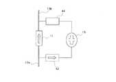
図1は、本発明による高周波スイッチの第一の実施形態の構成を示す平面図である。本実施形態は、高周波信号が通過する高周波伝達回路10とその信号の伝達を制御する駆動回路19からなる。高周波伝達回路10は、高周波導波路13aおよび13b、抵抗が電圧あるいは電流の向きによって変化する第一の可変デバイス11から構成されている。 FIG. 1 is a plan view showing a configuration of a first embodiment of a high-frequency switch according to the present invention. The present embodiment includes a high-
高周波導波路13aおよび13bは、マイクロストリップ導波路回路、コプレナー導波路回路等によって作製されたものであり、高周波信号を損失なく伝達するのに適したものである。例えば、厚さ2μm、40μmの幅の金配線からなる高周波導波路13aおよび13bをガラス等の絶縁性の基板18に設け、基板18の裏面に設けた金属薄膜をグラウンド電位とすることによって構成することができる。 The high-
外部の導波路回路(図示せず)の入射側に高周波導波路13a、出射側に高周波導波路13bを金ワイア等の手段によって接続を行う。高周波導波路13aおよび13bは、図示するように第一の可変デバイス11を介して接続している。第一の可変デバイス11は、可変抵抗層113、シリコン窒化膜等の絶縁膜115、上部電極111をこの順に堆積させた構成をもつ。 A high-
可変抵抗層113は、高周波導波路13aの上に、例えば200nmの厚さの銅と20nmの厚さの硫化銅を堆積させたものである。上部電極111は、例えば、厚さ2μm、幅30ミクロンの金等の金属から構成されており、絶縁膜115に設けられたコンタクト穴114を介して可変抵抗層113に接続している。また、上部電極111は、絶縁膜膜115に設けられたコンタクト穴112を介して高周波導波路13bに接続している。 The
第一の可変デバイス11は、高周波導波路13aから13bの向きに電流が流れるような電圧が印加されたときには小さな抵抗となり、その反対の向きに電流が流れるような電圧が印加されたときには10kΩ以上の抵抗をもつ。実際に作製したデバイスを測定したところ、高周波導波路13aから13bの向きに0.2Vの電圧を印加したとき(このとき約100mAの電流が流れる)に抵抗が2Ω以下、逆向きに0.06Vの電圧を印加したとき(このとき約1μA以下の電流が流れる)に100kΩの抵抗をもった。 The first
駆動回路19は、第二の可変デバイス12と約10kΩの値をもつ固定抵抗14から構成されており、外部の信号回路15と接続されている。第二の可変デバイス12は、可変抵抗層123、シリコン窒化膜等の絶縁膜125、上部電極121をこの順に堆積させた構成をもつ。可変抵抗層123は、金属配線17の上に例えば200nmの厚さの銅と20nmの厚さの硫化銅を堆積させたものである。 The
上部電極121は、例えば、厚さ0.2μm、幅30ミクロンの金等の金属から構成されており、絶縁膜125に設けられたコンタクト穴124を介して可変抵抗層123に接続している。また、上部電極121は、絶縁膜膜125に設けられたコンタクト穴122を介して高周波導波路13bに接続している。この第二の可変デバイス12は、金属配線17から高周波導波路13bの向きに電流が流れるような電圧が印加されたときにその抵抗が2Ω以下と小さくなる。そして、反対の向きに電流が流れるような電圧が印加されたときには10kΩ以上の大きな抵抗となるものである。 The
一方、固定抵抗14は、電流の向きや電圧の大きさにに依存せず、ほぼ同じ大きさの抵抗をもち、高周波導波路13aと金属配線16の間に設けられている。固定抵抗14は、例えば窒化タンタル等の高抵抗金属を用いて、幅5μm、長さ3mm、厚さ0.1μmの寸法をもつ。この固定抵抗は多重に折り返したパターンを利用すると占有する面積を小さくすることができる。二つの金属配線16および17は、アルミ、あるいは金等の金属からなり、例えば幅20μmで厚さが0.2である。 On the other hand, the fixed
信号回路15は、二つの金属配線16および17に接続されており、本実施形態の高周波スイッチを切り替える信号を提供する。具体的には駆動回路19に印加する電圧または駆動回路19を流れる電流を制御する信号を出力する。なお、この例では、二つの可変デバイス11および12がそれぞれ接続される高周波導波路13bからみてこの高周波導波路13bに向かう方向が抵抗が小さくなる順方向となっている。 The
次に、本実施形態のスイッチの動作を図2(a)および図2(b)を用いて説明する。同図において、図1と同じ番号は同様の構成要素を示すものである。 Next, the operation of the switch of the present embodiment will be described with reference to FIGS. 2 (a) and 2 (b). In the figure, the same numbers as those in FIG. 1 indicate the same components.
図2(a)は、駆動回路19に右回りの電流(図中)が流れるように信号回路15に制御信号を加えたときの様子を示している。このとき、第一の可変デバイス11は順方向にバイアスされるために抵抗が小さく(r)なるのに対して、第二の可変デバイス12は逆方向にバイアスされるために10kΩ以上の大きな抵抗値(R)をもつ。この状態のとき、高周波導波路13aに入力された高周波信号は、第一の可変デバイス11を低損失で通過して高周波導波路13b側に出射される。そして第二の可変デバイス12が接続されている分岐線側にほとんど漏れないため、高周波信号は高周波導波路13bを低損失で進行していくことができる。この状態は、信号回路15に逆向きの制御信号を加えるまで継続しており、途中に順方向の信号を加えつづける必要がない。 FIG. 2A shows a state when a control signal is applied to the
続いて、図2(b)は、駆動回路19に左回りの電流(図中)が流れるように信号回路15に制御信号を加えたときの様子を示している。始めに信号回路15に加えた電圧の約R/(R+R’)だけの値が第二の可変デバイス12に印加される。R’は固定抵抗14の値である。RとR’が共に約10kΩの場合には約半分の電圧が第二の可変デバイス12に印加されることになる。このとき、印加電圧あるいは電流が第二の可変デバイス12と順方向に印加されているために、第二の可変デバイス12は小さな抵抗値(r)に変化する。そして、第二の可変デバイス12の抵抗変化が急激に起こることから、第一の可変デバイス11の両端に大きな逆方向の電圧が印加され、その結果、第一の可変デバイス11は、大きな抵抗(R)を持つように変化する。高周波導波路13aに入力された高周波信号は、第一の可変デバイス11で反射されて高周波導波路13b側にほとんど出射されない。そして固定抵抗14が接続されている分岐線側にもほとんど漏れないので、高周波信号は高周波導波路13bを進行していくことができない。この状態は、信号回路15に順方向の制御信号を加えるまで継続しており、途中に逆方向の信号を加えつづける必要がない。 Next, FIG. 2B shows a state when a control signal is applied to the
次に、本実施形態の製造方法について図3(a)〜(d)は、第一の実施の形態を作製する方法を段階的に示す図であり、各図左側部分は平面図、右側部分はそのA−A’断面図である。 Next, FIGS. 3A to 3D are views showing the manufacturing method of the first embodiment step by step with respect to the manufacturing method of the present embodiment. Is a sectional view taken along the line AA ′.
最初に、ガラス基板30の裏面を金の薄膜によって覆い、グラウンド301を作製する。ガラス基板30の表側の面には、0.1μmの厚さの窒化クロムにより固定抵抗34のパターンを作製する。続いて、0.3μmの厚さの金で表側の面を覆い、導波路33aおよび33bの領域のみに金メッキにより金を1.7μm堆積する。その後、導波路33aおよび33b、そして、金属配線36および37のパターンをレジストにより作製し、このレジストをマスクにして0.3μmの金をエッチングする。最後に、このレジストを除去する(図3(a))。 First, the back surface of the
上記プロセスに続いて、ガラス基板30の上に0.2μm厚の銅薄膜を堆積させる。その後、この銅表面の一部を硫化する。硫化銅の作製方法の一つを以下に述べる。硫化ナトリウム溶液の中に基板30を入れ、硫化ナトリウム溶液に対して基板30に設けられた銅薄膜が正側にバイアスされるように電源を接続する。この間、約100μAの電流が流れるように設定して、20nm厚の硫化銅を作製する。この後,硫化銅および銅をエッチングしてパターン313および323を導波路33aおよび金属配線37の上にそれぞれ作製する(図3(b))。 Following the above process, a 0.2 μm thick copper thin film is deposited on the
さらに、厚さ約0.3μmの窒化シリコン膜を基板30に堆積させて、絶縁膜315および325のパターン作製を行う。絶縁膜パターン315の中には、硫化銅であるパターン313および金である導波路33bの表面が露出するようにコンタクト穴314および312を同時に作製する。また、絶縁膜パターン325の中には、パターン323および導波路33bの表面が露出するようにコンタクト穴324および322を同時に作製する(図3(c))。 Further, a silicon nitride film having a thickness of about 0.3 μm is deposited on the
続いて、基板30の上に0.3μm厚の金を堆積させ、さらに、電気メッキを用いて上部電極311の領域のみに約1.7μmの厚さの金を堆積させる。そして、レジストをマスクにして金をエッチングし、上部電極パターン311および321を作製する。最後に、このレジストを除去する(図3(d))。上部電極311は、絶縁膜315の中に設けられたコンタクト穴314および312を介してパターン313および導波路33bに電気的に接続している。また、上部電極321は、絶縁膜325の中に設けられたコンタクト穴324および322を介してパターン323および導波路33bに電気的に接続している。 Subsequently, gold having a thickness of 0.3 μm is deposited on the
図1の実施例中における第一の可変デバイス11の位置とコンタクト穴112の位置を入れ替えることも可能である。このとき、可変抵抗層113は、高周波導波路13bの上に硫化銅、銅の順に堆積される。このような構成にすると、第一の可変デバイス11の電流の向きに対する変化が変わらない。同様にして、第二の可変デバイス12の位置と他のコンタクト穴122の位置を変化の向きを変えることなく入れ替えることが可能である。 The position of the first
さらに、図1に示した例のように可変デバイス11および12を回路の接続箇所にそれぞれ唯一つだけ設けるという必要はない。上に述べたような構成を用いることによって、電流に対する抵抗の変化を変えることなく、回路の接続箇所の両端に可変デバイスを設けることも可能である。 Further, it is not necessary to provide only one
また、駆動回路19の第二の可変デバイス12を高周波導波路13bに接続させた例だけでなく、この第二の可変デバイス12を上部電極111に接続させることも可能である。この場合には、上部電極111と上部電極121をコンタクト穴を介さずに直接接続させることができる。 In addition to the example in which the second
上記の例では、二つの可変デバイス11および12がそれぞれ接続される高周波導波路13bからみて、該高周波導波路13bに向かう方向が抵抗の小さくなる順方向となっている。この向きを変えて、接続される高周波導波路13bからみて、該高周波導波路13bに向かう方向が抵抗の大きくなる逆方向に二つの可変デバイス11および12を配置しても本実施形態と同様の効果を得ることが可能である。 In the above example, when viewed from the high-
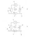
図4は、本発明の第二の実施形態の構成を示す等価回路図である。図中、図2と同じ番号は、同じ構成要素を示している。本実施形態では、固定抵抗44と第二の可変デバイス42の位置が第一の実施形態と入れ替わっている。また、第二の可変デバイス42の順方向の向きも第一の実施形態と反対である。本実施形態のスイッチの動作を図5(a)および(b)を用いて説明する。同図において図4と同じ番号は同様の構成要素を示すものである。 FIG. 4 is an equivalent circuit diagram showing the configuration of the second embodiment of the present invention. In the figure, the same numbers as those in FIG. 2 indicate the same components. In the present embodiment, the positions of the fixed
図5(a)は、駆動回路19に右回りの電流(図中)が流れるように信号回路15に制御信号を加えたときの様子を示している。このとき、第一の可変デバイス11は順方向にバイアスされるために抵抗が小さく(r)なるのに対して、第二の可変デバイス42は逆方向にバイアスされるために10kΩ以上の大きな抵抗値(R)をもつ。この状態のとき、高周波導波路13aに入力された高周波信号は、第一の可変デバイス11を低損失で通過して高周波導波路13b側に出射される。また、第二の可変デバイス42および固定抵抗44が接続されている分岐線側にほとんど漏れないため、高周波信号は高周波導波路13aおよび13bを低損失で進行していくことができる。この状態は、信号回路15に逆向きの制御信号を加えるまで継続しており、途中に順方向の信号を加えつづける必要がない。 FIG. 5A shows a state when a control signal is applied to the
続いて、図5(b)は、駆動回路19に左回りの電流(図中)が流れるように信号回路15に制御信号を加えたときの様子を示している。始めに信号回路15に加えた電圧の約R/(R+R’)だけの値が第二の可変デバイス42に印加される。R’は固定抵抗44の値である。RとR’が共に約10kΩの場合には約半分の電圧が第二の可変デバイス42に印加されることになる。このとき、印加電圧あるいは電流が第二の可変デバイス42と順方向に印加されているために、第二の可変デバイス42は小さな抵抗値(r)に変化する。そして、この第二の可変デバイス42の抵抗変化が急激に起こることから第一の可変デバイス11の両端に大きな逆方向の電圧が印加され、その結果、第一の可変デバイス11は、大きな抵抗(R)を持つように変化する。高周波導波路13aに入力された高周波信号は、第一の可変デバイス11で反射されて高周波導波路13b側にほとんど出射されない。そして固定抵抗44が接続されているため、この分岐を通って高周波信号が高周波導波路13bに進入していくことができない。この状態は、信号回路15に順方向の制御信号を加えるまで継続しており、途中に逆方向の信号を加えつづける必要がない。 Subsequently, FIG. 5B shows a state when a control signal is applied to the
なお、本実施形態では、二つの可変デバイス11および12がそれぞれ接続される高周波導波路13aからみてこの高周波導波路13aに向かう方向が抵抗の大きくなる逆方向となっている。この向きを変えて、接続される高周波導波路13aからみてこの高周波導波路13aに向かう方向が抵抗の小さくなる順方向に二つの可変デバイス11および42を配置しても本実施形態と同様の効果を得ることが可能である。 In the present embodiment, the direction toward the high-
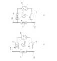
図6は、本発明の第三の実施形態の構成を示す等価回路図である。図6中で図2と同じ番号は、同じ構成要素を示している。本実施形態では、固定抵抗の位置に可変デバイス62が設けられており、駆動回路に二つの可変デバイスが設けられている。また、二つの可変デバイス11および12がそれぞれ接続される高周波導波路13bからみてこの高周波導波路13bに向かう方向が抵抗の小さくなる順方向となっている。一方、二つの可変デバイス11および62が接続される高周波導波路13aからみてこの高周波導波路13aに向かう方向が抵抗の大きくなる逆方向となっている。このような構成においても、前述した実施形態と同様の効果を得ることが可能である。 FIG. 6 is an equivalent circuit diagram showing the configuration of the third embodiment of the present invention. In FIG. 6, the same numbers as those in FIG. 2 indicate the same components. In this embodiment, the
なお、本実施形態の構成を変えて、二つの可変デバイス11および12がそれぞれ接続される高周波導波路13bからみてこの高周波導波路13bに向かう方向が抵抗の大きくなる逆方向に二つの可変デバイス11および62を配置し、接続される高周波導波路13aからみてこの高周波導波路13aに向かう方向が抵抗の小さくなる順方向に二つの可変デバイス11および62を配置しても本発明と同様の効果を得ることが可能である。 Note that, by changing the configuration of the present embodiment, the two
図7は、本発明の第四の実施形態の構成を示す等価回路図である。図7中で図2と同じ番号は、同じ構成要素を示している。本実施形態では、固定抵抗がなくなり、高周波導波路13a側にバイアス回路70が接続されている。バイアス回路70は、例えばバイパスコンデンサ701とバイアスコイル702を図示するように接続したものである。バイアスコイル702の他方の端には、所定のバイアス電圧あるいはグラウンド電位になるように接続がなされている。バイアス回路70は、高周波スイッチの内部に含まれることとしても良いし、あるいは外部に設けて高周波スイッチに接続しても良い。また、信号回路15は、一端が第二の可変デバイス12に接続され、他端がグラウンドあるいはあるバイアス電位に接続されている。本実施形態では、可変デバイス11および12がそれぞれ接続される高周波導波路13bからみてこの高周波導波路13bに向かう方向が抵抗の小さくなる順方向となっている。このような構成においても、前述の実施形態と同様の効果を得ることが可能である。 FIG. 7 is an equivalent circuit diagram showing a configuration of the fourth embodiment of the present invention. In FIG. 7, the same numbers as those in FIG. 2 indicate the same components. In this embodiment, there is no fixed resistance, and the
なお、上記の構成に変えて、二つの可変デバイス11および12が接続される高周波導波路13bからみてこの高周波導波路13bに向かう方向が抵抗の大きくなる逆方向となるようにしてもよい。 Instead of the above configuration, the direction toward the high-
また、本実施形態では、硫化銅を用いた可変抵抗デバイスを利用して可変デバイスを作製した。しかし、この可変抵抗デバイスの可変抵抗層は硫化銅に制限されることなく、広くカルコゲナイド(砒素、ゲルマニウム、セレニウム、テリュウム、ビスマス、ニッケル、硫黄、ポロニウム、亜鉛等)と周期表のIとIIの金属の化合物を用いることが可能である。 In this embodiment, a variable device is manufactured using a variable resistance device using copper sulfide. However, the variable resistance layer of this variable resistance device is not limited to copper sulfide, but is broadly chalcogenide (arsenic, germanium, selenium, terium, bismuth, nickel, sulfur, polonium, zinc, etc.) and I and II of the periodic table. Metal compounds can be used.
10 高周波伝達回路
11 第一の可変デバイス
12 第二の可変デバイス
13a,13b,33a,33b 高周波導波路
14 固定抵抗
15 信号回路
16,17 金属配線
18 基板
19 駆動回路
30 ガラス基板
111,121 上部電極
112,114,122,14,312,22,324 コンタクト穴
113,123 可変抵抗層
115,125 絶縁膜
121,311,321 上部電極
301 グラウンド
313,323パターン
315,325 絶縁膜
DESCRIPTION OF
Claims (6)
Translated fromJapanese前記導波路とともに前記可変デバイスが少なくとも一つ設けられる高周波伝達回路と、
前記可変デバイスが少なくとも一つ設けられる駆動回路と、
前記高周波伝達回路および前記駆動回路に設けられる前記可変デバイスへの電流供給状態を変化させることにより、各可変デバイスの状態を変化させる信号回路と、を有し、
前記駆動回路と前記高周波伝達回路とが電気的に接続されるとともに、該接続点から見て、前記高周波伝達回路に設けられた可変デバイスと前記駆動回路に設けられた可変デバイスの状態が異なるように各可変デバイスが配置されていることを特徴とする高周波スイッチ。A high-frequency switch that changes a signal passing through a waveguide using a variable device that has a first state with a large resistance value and a second state with a small resistance value depending on the direction of current flow,
A high-frequency transmission circuit provided with at least one of the variable devices together with the waveguide;
A drive circuit provided with at least one of the variable devices;
A signal circuit that changes a state of each variable device by changing a current supply state to the variable device provided in the high-frequency transmission circuit and the drive circuit;
The drive circuit and the high-frequency transmission circuit are electrically connected, and the state of the variable device provided in the high-frequency transmission circuit is different from the state of the variable device provided in the drive circuit when viewed from the connection point. Each of the variable devices is arranged in a high frequency switch.
駆動回路が、値がほぼ変化しない抵抗を含んでおり、
信号回路は、駆動回路に設けられた可変デバイスを介して高周波伝達回路に設けられた可変デバイスの一端と接続され、前記抵抗を介して高周波伝達回路に設けられた可変デバイスの他端と接続されることを特徴とする高周波スイッチ。The high frequency switch according to claim 1,
The drive circuit includes a resistor whose value does not change substantially,
The signal circuit is connected to one end of a variable device provided in the high-frequency transmission circuit via a variable device provided in the drive circuit, and is connected to the other end of the variable device provided in the high-frequency transmission circuit via the resistor. A high-frequency switch characterized by that.
ほぼ変化しない抵抗の値が10kΩ以上であることを特徴とする高周波スイッチ。The high frequency switch according to claim 2,
A high-frequency switch characterized in that the resistance value which does not substantially change is 10 kΩ or more.
駆動回路が、第一および第二の可変デバイスを含んでおり、
信号回路は、駆動回路に設けられた第一の可変デバイスを介して高周波伝達回路に設けられた可変デバイスの一端と接続され、第二の可変デバイスを介して高周波伝達回路に設けられた可変デバイスの他端と接続されることを特徴とする高周波スイッチ。The high frequency switch according to claim 1,
The drive circuit includes first and second variable devices;
The signal circuit is connected to one end of the variable device provided in the high-frequency transmission circuit via the first variable device provided in the drive circuit, and the variable device provided in the high-frequency transmission circuit via the second variable device A high-frequency switch connected to the other end of the switch.
高周波伝達回路に設けられた可変デバイスの他端にバイアス回路が設けられ、
信号回路は、駆動回路に設けられた可変デバイスを介して高周波伝達回路に設けられた可変デバイスの一端と接続されるとともに、バイアス電位に接続されることを特徴とする高周波スイッチ。The high frequency switch according to claim 1,
A bias circuit is provided at the other end of the variable device provided in the high-frequency transmission circuit,
The signal circuit is connected to one end of a variable device provided in the high-frequency transmission circuit via a variable device provided in the drive circuit, and is connected to a bias potential.
可変デバイスの抵抗が1Ω以下と10kΩ以上の領域の間を変化することを特徴とする高周波スイッチ。In the high frequency switch in any one of Claim 1 to 5,
A high-frequency switch characterized in that the resistance of the variable device changes between the region of 1Ω or less and 10kΩ or more.
Priority Applications (2)
| Application Number | Priority Date | Filing Date | Title |
|---|---|---|---|
| JP2003416693AJP4310633B2 (en) | 2003-12-15 | 2003-12-15 | High frequency switch |
| US11/011,914US7321274B2 (en) | 2003-12-15 | 2004-12-14 | RF switch |
Applications Claiming Priority (1)
| Application Number | Priority Date | Filing Date | Title |
|---|---|---|---|
| JP2003416693AJP4310633B2 (en) | 2003-12-15 | 2003-12-15 | High frequency switch |
Publications (2)
| Publication Number | Publication Date |
|---|---|
| JP2005176215A JP2005176215A (en) | 2005-06-30 |
| JP4310633B2true JP4310633B2 (en) | 2009-08-12 |
Family
ID=34650638
Family Applications (1)
| Application Number | Title | Priority Date | Filing Date |
|---|---|---|---|
| JP2003416693AExpired - Fee RelatedJP4310633B2 (en) | 2003-12-15 | 2003-12-15 | High frequency switch |
Country Status (2)
| Country | Link |
|---|---|
| US (1) | US7321274B2 (en) |
| JP (1) | JP4310633B2 (en) |
Families Citing this family (2)
| Publication number | Priority date | Publication date | Assignee | Title |
|---|---|---|---|---|
| US20160301249A1 (en)* | 2015-04-09 | 2016-10-13 | Infineon Technologies Ag | Communicating between galvanically isolated devices using waveguides |
| CN114362785B (en)* | 2021-12-29 | 2023-11-17 | 贸联电子(昆山)有限公司 | High-frequency signal switching device and tester and test system with same |
Family Cites Families (10)
| Publication number | Priority date | Publication date | Assignee | Title |
|---|---|---|---|---|
| US5761115A (en)* | 1996-05-30 | 1998-06-02 | Axon Technologies Corporation | Programmable metallization cell structure and method of making same |
| JPH11274805A (en) | 1998-03-20 | 1999-10-08 | Ricoh Co Ltd | High frequency switch, manufacturing method, and integrated high frequency switch array |
| JPH11340704A (en) | 1998-05-21 | 1999-12-10 | Mitsubishi Electric Corp | High frequency switch |
| JP3374804B2 (en)* | 1999-09-30 | 2003-02-10 | 日本電気株式会社 | Phase shifter and method of manufacturing the same |
| JP3356139B2 (en)* | 1999-10-29 | 2002-12-09 | 日本電気株式会社 | Phase shifter |
| JP4356188B2 (en) | 2000-04-07 | 2009-11-04 | 株式会社デンソー | High frequency switch and driving method of high frequency switch |
| JP2002252553A (en) | 2001-02-23 | 2002-09-06 | Matsushita Electric Works Ltd | Driving circuit for semiconductor device and semiconductor device |
| JP3631693B2 (en) | 2001-05-17 | 2005-03-23 | 埼玉日本電気株式会社 | High frequency switching circuit and switching operation monitoring method thereof |
| JP2003101393A (en) | 2001-09-25 | 2003-04-04 | Matsushita Electric Works Ltd | Semiconductor device and sample-and-hold circuit using the same |
| US6812810B2 (en)* | 2002-06-19 | 2004-11-02 | Intel Corporation | Bridges for microelectromechanical structures |
- 2003
- 2003-12-15JPJP2003416693Apatent/JP4310633B2/ennot_activeExpired - Fee Related
- 2004
- 2004-12-14USUS11/011,914patent/US7321274B2/ennot_activeExpired - Fee Related
Also Published As
| Publication number | Publication date |
|---|---|
| US20050128026A1 (en) | 2005-06-16 |
| JP2005176215A (en) | 2005-06-30 |
| US7321274B2 (en) | 2008-01-22 |
Similar Documents
| Publication | Publication Date | Title |
|---|---|---|
| Chakraborty et al. | Paradigm phase shift: RF MEMS phase shifters: An overview | |
| CN101202369B (en) | Miniature MEMS switching line phase shifter | |
| KR20060041676A (en) | Variable resonators and variable idealizers | |
| Wu et al. | Circuits and antennas incorporating gallium-based liquid metal | |
| JPWO2006011239A1 (en) | Capacitive MEMS element, manufacturing method thereof, and high-frequency device | |
| JP6167006B2 (en) | Waveguide substrate | |
| CN114520222B (en) | Passive filter and preparation method thereof | |
| US8410469B2 (en) | Chalcogenide nanoionic-based radio frequency switch | |
| Shafai et al. | Microstrip phase shifter using ground-plane reconfiguration | |
| JP2008277743A (en) | Variable element circuit and manufacturing method thereof | |
| Nessel et al. | A novel nanoionics-based switch for microwave applications | |
| JP4310633B2 (en) | High frequency switch | |
| CN115241163B (en) | Adjustable filter and preparation method thereof | |
| US20050270127A1 (en) | Micro-electromechanical switching device | |
| JP3841305B2 (en) | Variable resonator and variable phase shifter | |
| CN216290855U (en) | Tunable filter | |
| WO2003015128A2 (en) | An electromechanical switch and method of fabrication | |
| TWI778214B (en) | Electronic products having embedded porous dielectric, related semiconductor products, and their methods of manufacture | |
| Daneshmand | Multi-port RF MEMS switches and switch matrices | |
| JP6858825B2 (en) | Direct flat-paste type active frequency-selective surface switch element and its manufacturing method | |
| Baghchehsaraei et al. | Waveguide‐integrated MEMS‐based phase shifter for phased array antenna | |
| US6191754B1 (en) | Antenna system using time delays with mercury wetted switches | |
| US6989500B2 (en) | Liquid metal contact reed relay with integrated electromagnetic actuator | |
| Dacuycuy et al. | Electrically Actuated Liquid-Metal Unit Cell for an Intelligent Reflecting Surface | |
| KR20060090021A (en) | Piezoelectric drive type resistance MFC MEMS switch and manufacturing method thereof |
Legal Events
| Date | Code | Title | Description |
|---|---|---|---|
| RD04 | Notification of resignation of power of attorney | Free format text:JAPANESE INTERMEDIATE CODE: A7424 Effective date:20060206 | |
| A621 | Written request for application examination | Free format text:JAPANESE INTERMEDIATE CODE: A621 Effective date:20061114 | |
| A977 | Report on retrieval | Free format text:JAPANESE INTERMEDIATE CODE: A971007 Effective date:20090226 | |
| TRDD | Decision of grant or rejection written | ||
| A01 | Written decision to grant a patent or to grant a registration (utility model) | Free format text:JAPANESE INTERMEDIATE CODE: A01 Effective date:20090415 | |
| A01 | Written decision to grant a patent or to grant a registration (utility model) | Free format text:JAPANESE INTERMEDIATE CODE: A01 | |
| A61 | First payment of annual fees (during grant procedure) | Free format text:JAPANESE INTERMEDIATE CODE: A61 Effective date:20090428 | |
| FPAY | Renewal fee payment (event date is renewal date of database) | Free format text:PAYMENT UNTIL: 20120522 Year of fee payment:3 | |
| R150 | Certificate of patent or registration of utility model | Free format text:JAPANESE INTERMEDIATE CODE: R150 | |
| LAPS | Cancellation because of no payment of annual fees |