JP4310589B2 - Wireless IC device inspection system and wireless IC device manufacturing method using the same - Google Patents
Wireless IC device inspection system and wireless IC device manufacturing method using the sameDownload PDFInfo
- Publication number
- JP4310589B2 JP4310589B2JP2008530884AJP2008530884AJP4310589B2JP 4310589 B2JP4310589 B2JP 4310589B2JP 2008530884 AJP2008530884 AJP 2008530884AJP 2008530884 AJP2008530884 AJP 2008530884AJP 4310589 B2JP4310589 B2JP 4310589B2
- Authority
- JP
- Japan
- Prior art keywords
- wireless
- inspection system
- inspection
- probe
- radiation plate
- Prior art date
- Legal status (The legal status is an assumption and is not a legal conclusion. Google has not performed a legal analysis and makes no representation as to the accuracy of the status listed.)
- Expired - Fee Related
Links
Images


Classifications
- G—PHYSICS
- G01—MEASURING; TESTING
- G01R—MEASURING ELECTRIC VARIABLES; MEASURING MAGNETIC VARIABLES
- G01R1/00—Details of instruments or arrangements of the types included in groups G01R5/00 - G01R13/00 and G01R31/00
- G01R1/02—General constructional details
- G01R1/06—Measuring leads; Measuring probes
- G01R1/067—Measuring probes
- G01R1/06788—Hand-held or hand-manipulated probes, e.g. for oscilloscopes or for portable test instruments
- G—PHYSICS
- G06—COMPUTING OR CALCULATING; COUNTING
- G06K—GRAPHICAL DATA READING; PRESENTATION OF DATA; RECORD CARRIERS; HANDLING RECORD CARRIERS
- G06K19/00—Record carriers for use with machines and with at least a part designed to carry digital markings
- G06K19/06—Record carriers for use with machines and with at least a part designed to carry digital markings characterised by the kind of the digital marking, e.g. shape, nature, code
- G06K19/067—Record carriers with conductive marks, printed circuits or semiconductor circuit elements, e.g. credit or identity cards also with resonating or responding marks without active components
- G06K19/07—Record carriers with conductive marks, printed circuits or semiconductor circuit elements, e.g. credit or identity cards also with resonating or responding marks without active components with integrated circuit chips
- G06K19/0722—Record carriers with conductive marks, printed circuits or semiconductor circuit elements, e.g. credit or identity cards also with resonating or responding marks without active components with integrated circuit chips comprising an arrangement for testing the record carrier
- G—PHYSICS
- G01—MEASURING; TESTING
- G01R—MEASURING ELECTRIC VARIABLES; MEASURING MAGNETIC VARIABLES
- G01R1/00—Details of instruments or arrangements of the types included in groups G01R5/00 - G01R13/00 and G01R31/00
- G01R1/02—General constructional details
- G01R1/06—Measuring leads; Measuring probes
- G01R1/067—Measuring probes
- G01R1/06772—High frequency probes
- G—PHYSICS
- G01—MEASURING; TESTING
- G01R—MEASURING ELECTRIC VARIABLES; MEASURING MAGNETIC VARIABLES
- G01R31/00—Arrangements for testing electric properties; Arrangements for locating electric faults; Arrangements for electrical testing characterised by what is being tested not provided for elsewhere
- G01R31/28—Testing of electronic circuits, e.g. by signal tracer
- G01R31/282—Testing of electronic circuits specially adapted for particular applications not provided for elsewhere
- G01R31/2822—Testing of electronic circuits specially adapted for particular applications not provided for elsewhere of microwave or radiofrequency circuits
Landscapes
- Physics & Mathematics (AREA)
- General Physics & Mathematics (AREA)
- Engineering & Computer Science (AREA)
- Computer Hardware Design (AREA)
- Microelectronics & Electronic Packaging (AREA)
- Theoretical Computer Science (AREA)
- Testing Of Individual Semiconductor Devices (AREA)
Description
Translated fromJapanese本発明は、無線ICデバイス、特に、RFID(Radio Frequency Identification)システムに用いられる無線ICデバイスの検査システム及びそれを用いた無線ICデバイスの製造方法に関する。 The present invention relates to a wireless IC device, in particular, a wireless IC device inspection system used in an RFID (Radio Frequency Identification) system and a method of manufacturing a wireless IC device using the same.
近年、RFID(Radio Frequency Identification)と称される非接触型識別媒体(非接触型IDカード等)に関する技術が急速に進歩してきており、その使用も多岐にわたっている。このようなRFIDは、リーダ・ライタとの間で性能に応じた通信距離が定められており、通信測定の向上及び歩留りの向上が望まれている。 In recent years, a technology related to a non-contact type identification medium (non-contact type ID card or the like) called RFID (Radio Frequency Identification) has been rapidly advanced, and its use has been various. In such RFID, a communication distance according to performance is determined between the reader / writer and an improvement in communication measurement and a yield are desired.
従来、RFIDシステムに用いられる無線ICデバイスは、フィルムベース上にアンテナコイルが形成され、これに無線ICチップが搭載されたものとして、これらが製造段階で所定大のフィルムベース上に所定数形成されるのが一般的となっている。そして、単体とされる前に検査対象の単一の無線ICデバイスごとに特性の測定を行い、製品の良否を検査することが行われている。 Conventionally, in a wireless IC device used in an RFID system, an antenna coil is formed on a film base, and a wireless IC chip is mounted on the antenna coil. A predetermined number of these are formed on a film base having a predetermined size at the manufacturing stage. It has become common. In addition, before a single device is used, characteristics are measured for each single wireless IC device to be inspected to inspect the quality of the product.
しかしながら、前述のような検査を行う場合、無線ICデバイスが単体として形成される前の段階で行われることから、RFIDリーダ・ライタからの通信に対する応答が、本来の検査対象の検査片からのものと、隣接された無線ICデバイスからのものとが混在して受信される。その場合、受信データの信頼性がなくなるだけでなく、検査対象の検査片が不良品の場合、隣接された無線ICデバイスからのデータが受信されて、検査片が本来不良品であるにも拘わらず、良品と判定されることとなり、不良品が流出してしまうという問題がある。 However, when performing the inspection as described above, since the wireless IC device is performed before it is formed as a single unit, the response to the communication from the RFID reader / writer is from the original inspection target inspection piece. And those from adjacent wireless IC devices are received together. In this case, not only the reliability of the received data is lost, but also when the inspection piece to be inspected is a defective product, data from the adjacent wireless IC device is received and the inspection piece is originally a defective product. Therefore, it is determined that the product is a non-defective product, and there is a problem that a defective product flows out.
特許文献1及び2には、検査対象の近傍の無線ICデバイスとの混信を回避させるために、検査対象の無線ICデバイスと測定システム側アンテナとの間に開口部を形成したシールド部材を介在させ、該開口部で測定システム側アンテナを検査対象の無線ICデバイスのみと対向させている。このような構造にすることで、RFIDリーダ・ライタからの通信に対する応答が、本来の検査対象の無線ICデバイスからのものと、隣接された無線ICデバイスからのものとが混在して受信されることを防ぐ検査システムが開示されている。 In
このような検査システムの検査対象は、アンテナと無線ICチップを少なくとも備えており、このようなアンテナを備えた無線ICデバイスはアンテナ部分が非常に大きいため、検査システムの搬送ベルトでの無線ICデバイスどうしの間隔は、少なくとも約一つ分の無線ICデバイスの大きさが必要となっていた。このため、一個の無線ICデバイスを検査するための搬送ベルトの移動量が大きく、検査時間が長くなり検査コストが高くなるという問題点があった。 The inspection target of such an inspection system includes at least an antenna and a wireless IC chip. Since the wireless IC device including such an antenna has a very large antenna portion, the wireless IC device on the transport belt of the inspection system The interval between the radio IC devices is required to be at least about one size. For this reason, there has been a problem that the amount of movement of the conveyor belt for inspecting one wireless IC device is large, the inspection time is long, and the inspection cost is high.
また、アンテナと無線ICチップを少なくとも備えた無線ICデバイスは、アンテナ電極が形成されたフィルムに無線ICチップを実装し、アンテナ電極と無線ICチップを電気的に接続させる工程が必要であり、製造時間の大きな部分をこの製造工程が占めており、製造コストを高くする原因となっていた。
本発明は前述した実情に鑑みてなされたものであり、その目的は、個々の無線ICデバイスの特性を短時間で確実に測定することのできる無線ICデバイスの検査システム及びそれを用いた無線ICデバイスの製造方法を提供することにある。 The present invention has been made in view of the above-described circumstances, and an object of the present invention is to provide a wireless IC device inspection system capable of reliably measuring characteristics of individual wireless IC devices in a short time and a wireless IC using the same. It is to provide a device manufacturing method.
本発明に係る無線ICデバイスの検査システムは、無線ICチップと放射板とを備えた無線ICデバイスの検査システムであって、前記放射板の一部分に検査装置のプローブを直接接触させ、無線ICデバイスの特性を測定することを特徴とする。 A wireless IC device inspection system according to the present invention is a wireless IC device inspection system including a wireless IC chip and a radiation plate, and a probe of an inspection apparatus is brought into direct contact with a part of the radiation plate, thereby the wireless IC device. It is characterized by measuring the characteristics of
本発明に係る無線ICデバイスの検査システムにおいては、検査装置のプローブを放射板の一部分に直接接触させて無線ICデバイスの特性を測定するため、小電力の検査信号であってもプローブから放射板を経由して無線ICチップに直接に供給される。このため、検査信号が誤りなく被検査対象の無線ICデバイスに入力される。また、被検査対象である無線ICデバイスからの送信データが放射板からプローブを直接的に経由して検査装置に送信されるので、隣接する無線ICデバイスが測定に干渉することがなくなる。そして、多数の無線ICデバイスを連続して検査する場合、無線ICデバイスの間隔を詰めても測定に差し支えることはなく、検査時間、ひいては製造時間が短縮化される。 In the wireless IC device inspection system according to the present invention, the probe of the inspection apparatus is directly brought into contact with a part of the radiation plate to measure the characteristics of the wireless IC device. Is directly supplied to the wireless IC chip via For this reason, the inspection signal is input to the wireless IC device to be inspected without error. In addition, since transmission data from the wireless IC device to be inspected is transmitted from the radiation plate directly to the inspection apparatus via the probe, adjacent wireless IC devices do not interfere with the measurement. When a large number of wireless IC devices are inspected continuously, even if the intervals between the wireless IC devices are reduced, the measurement is not hindered, and the inspection time and thus the manufacturing time is shortened.
本発明に係る無線ICデバイスの検査システムにおいて、前記プローブは前記放射板の開放端に接触させることが好ましい。給電回路基板を実装した端部から開放端までの放射板の断線や、放射板全体の放射特性を検査できる。また、前記無線ICデバイスは、無線ICチップが搭載され、インダクタンス素子を含む共振回路を有する給電回路基板を備えており、該給電回路基板は放射板と電磁界結合していてもよい。また、前記プローブの先端は平板であることが好ましい。直接接触する放射板の表面部分を損傷することがなく、密着性、安定性が向上する。また、磁界結合で検査する場合は、プローブの先端部分をコイル状とすることにより、容易に検査することができる。 In the wireless IC device inspection system according to the present invention, it is preferable that the probe is brought into contact with an open end of the radiation plate. Disconnection of the radiation plate from the end where the feeder circuit board is mounted to the open end and the radiation characteristics of the entire radiation plate can be inspected. The wireless IC device may include a power supply circuit board having a resonance circuit including an inductance element on which a wireless IC chip is mounted, and the power supply circuit board may be electromagnetically coupled to the radiation plate. The probe tip is preferably a flat plate. Adhesion and stability are improved without damaging the surface portion of the radiation plate that is in direct contact. Further, when inspecting by magnetic field coupling, it is possible to easily inspect by making the tip portion of the probe into a coil shape.
また、本発明に係る無線ICデバイスの製造方法は、前記無線ICデバイスの検査システムを用いて無線ICデバイスを製造することを特徴とする。 A method of manufacturing a wireless IC device according to the present invention is characterized in that a wireless IC device is manufactured using the wireless IC device inspection system.
本発明によれば、無線ICチップと放射板とを備えた無線ICデバイスの特性を誤りなく、かつ、効率よく検査することができ、ひいては無線ICデバイスを短時間で効率よく製造することができる。 According to the present invention, the characteristics of a wireless IC device including a wireless IC chip and a radiation plate can be inspected without error and efficiently, and thus the wireless IC device can be efficiently manufactured in a short time. .
以下に、本発明に係る無線ICデバイスの検査システム及びそれを用いた無線ICデバイスの製造方法の実施例について添付図面を参照して説明する。なお、各図において無線ICデバイスと検査システムは模式的に示されており、各部品の縮尺比率は一致していない。 Embodiments of a wireless IC device inspection system and a wireless IC device manufacturing method using the same according to the present invention will be described below with reference to the accompanying drawings. In each figure, the wireless IC device and the inspection system are schematically shown, and the scale ratios of the components do not match.
(無線ICデバイス、図1〜図3参照)
まず、本発明の検査システムの対象となる無線ICデバイスについて説明する。図1〜図3に示すように、無線ICデバイス1は、無線ICチップ2と金属薄膜からなる放射板3とを備え(第1例、図1及び図3参照)、あるいは、無線ICチップ2と給電回路基板6と放射板3とを備え(第2例、図2参照)、RFIDシステムにおいてリーダ・ライタからの受信及び発信デバイスとして機能する。この無線ICデバイス1は、例えば、従来使用されているPOSシステムのバーコードに代えて使用されたり、流通管理や固定資産管理などに用いられる。(Wireless IC device, see FIGS. 1 to 3)
First, a wireless IC device that is an object of the inspection system of the present invention will be described. As shown in FIGS. 1 to 3, the
無線ICチップ2は、クロック回路、ロジック回路、メモリ回路を含み、必要な情報がメモリされており、直接もしくは給電回路基板6を介して、放射板3と接続されている。放射板3は、アルミ箔や銅箔などの非磁性体からなる長尺体、即ち、両端開放型の金属薄膜であり、PETなどの絶縁性のフレキシブルな樹脂フィルム4上に形成されている。 The
この無線ICデバイス1は、リーダ・ライタから放射される高周波信号を放射板3で受信し、受信信号を無線ICチップ2に供給する。一方、無線ICチップ2は、受信信号から所定のエネルギーを取り出し、このエネルギーを駆動源として無線ICチップ2にメモリされている情報を入力信号に反射変調を与えて送信信号とし、放射板3からリーダ・ライタに送信する。また、給電回路基板6は、無線ICチップ2と放射板3とのインピーダンス整合をとるためのインダクタンス素子を含む給電回路を内蔵している。 The
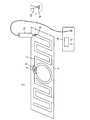
(検査システム、図1〜図3参照)
図1に無線ICデバイス1の検査システムの第1実施例を示す。この検査システムは、検査装置10に接続されたプローブ15の先端を前記放射板3の一部分に直接接触させ、プローブ15の先端と放射板3を電磁界結合させ、無線ICデバイス1の特性を測定する。プローブ15の先端は平板16とされ、放射板3との接触時の安定性、密着性を図っている。また、放射板3を損傷することも防止される。この検査時において、放射板3の開放端にプローブ15の先端を接触させることが好ましい。プローブ15の先端を放射板3の開放端に接触させることで、給電回路基板6の実装端部から開放端部までの放射板3の良否を判別できる。また、放射板3の全体を含めた無線ICデバイス1としての放射特性を検査することもできる。(Inspection system, see FIGS. 1 to 3)
FIG. 1 shows a first embodiment of an inspection system for a
検査装置10のメモリには、無線ICデバイス1の検査項目とRFIDシステムのスペック(使用周波数、コマンド等)が全て内蔵されており、その検査項目に従って無線ICデバイス1の検査を行う。 The memory of the
具体的には、無線ICデバイス1に使用されるRFIDシステムの種類、測定周波数やデータのやり取りに使用するコマンド(デジタルデータで何を意味しているかを示すシステム特有のもの)を設定するとともに、その無線ICデバイス1の検査項目を設定する。そして、検査装置10に接続されたプローブ15を放射板3に接触した状態にした後、検査装置10の発信部から無線ICチップ2に送信する情報の信号(例えば周波数偏位変調された信号)がプローブ15に送信される。 Specifically, while setting the type of RFID system used for the
無線ICチップ2は、プローブ15から放射板3で受信した信号を復調及びデータ処理し、検査装置10に送る必要があるデータを送信データ信号にし、該送信データ信号を放射板3から電磁界結合によりプローブ15に送信する。この送信データ信号は、プローブ15で受信され検査装置10に送られる。 The
検査装置10では、得られたデータ信号を、復調及びデータ処理を行った後、無線ICデバイス1が検査項目の全てを満足しているかを判断する。そして、検査項目を満足している場合には検査した無線ICデバイス1を良品と判断し、検査項目を満足していない場合には不良品であると判断する。 The
前述した検査時において、プローブ15の先端が放射板3と直接接触しているため、小電力の検査信号であってもプローブ15から放射板3を経由して無線ICチップ2に供給され、周囲に多数の無線ICデバイスが並置されていても(図4及び図5参照)、検査信号が誤りなく被検査対象の無線ICデバイス1に入力される。 Since the tip of the
また、被検査対象である無線ICデバイス1からの送信データ信号が放射板3からプローブ15を直接的に経由して検査装置10に送信されるので、隣接する無線ICデバイスが測定に干渉することがなくなる。そして、多数の無線ICデバイス1を連続して検査する場合、無線ICデバイス1の間隔を詰めても測定に差し支えることはなく、検査時間、ひいては製造時間が短縮化される。 Further, since the transmission data signal from the
なお、プローブ15の先端部でのインピーダンスが放射板3を含めた無線ICデバイス1のインピーダンスにほぼ等しくなるようにプローブ15の形状を変えることにより、種々のインピーダンスの無線ICデバイス1を検査することができる。 Note that the
図2に、給電回路基板6を備えた無線ICデバイス1の検査システムを示す。この検査システムは図1に示した検査システムと同じものである。なお、給電回路基板6は、放射板3と電磁界結合するように絶縁して配置している。このため、プローブ15の接触時の過電流などが無線ICチップ2に加わらないため、無線ICチップ2を保護することができる。 FIG. 2 shows an inspection system for the
図3に無線ICデバイス1の検査システムの第2実施例を示す。この検査システムは、検査装置10に接続されたプローブ15を備えている点で前記第1実施例と同様である。異なるのは、プローブ15の先端部分が磁界発生部を有すること、具体的には、先端部分をループ状のコイル状部分17とした点にあり、コイル状部分17の一部は放射板3のパターンに直接接触する。 FIG. 3 shows a second embodiment of the inspection system for the
本第2実施例は前記第1実施例と同様の作用効果を奏し、特に、放射板3に直接接触する部分をコイル状部分17としたため、プローブ15と放射板3とが磁界結合する。また、プローブ15の放射板3に対する密着性、安定性がより向上する。 The second embodiment has the same effect as the first embodiment, and in particular, since the portion directly contacting the
(無線ICデバイスの製造工程における検査工程例1)
次に、無線ICデバイス1の製造工程における検査工程例1について図4を参照して説明する。この検査工程例1において、多数の無線ICデバイス1は剛性を有する支持台板21上にマトリクス状に並置され、支持台板21又はプローブ15のいずれかをX−Y方向に移動させることで、多数の無線ICデバイス1を順次検査していく。(Example 1 of inspection process in wireless IC device manufacturing process)
Next, an inspection process example 1 in the manufacturing process of the
(無線ICデバイスの製造工程における検査工程例2)
次に、無線ICデバイス1の製造工程における検査工程例2について図5を参照して説明する。この検査工程例2において、多数の無線ICデバイス1は剛性を有する支持台板22上に並置され、矢印Y方向に間欠的に搬送される。そして、プローブ15によって所定位置Aに到達した無線ICデバイス1を順次検査していく。(Inspection process example 2 in wireless IC device manufacturing process)
Next, an inspection process example 2 in the manufacturing process of the
(他の実施例)
なお、本発明に係る無線ICデバイスの検査システム及び無線ICデバイスの製造方法は、前記実施例に限定するものではなく、その要旨の範囲内で種々に変更することができる。(Other examples)
Note that the wireless IC device inspection system and wireless IC device manufacturing method according to the present invention are not limited to the above-described embodiments, and can be variously modified within the scope of the gist thereof.
例えば、プローブ15の形状などの細部は任意であり、また、無線ICデバイスの放射板の形状や、放射板と無線ICチップの接続構造なども任意である。 For example, details such as the shape of the
以上のように、本発明は、無線ICデバイスの検査システムに有用であり、特に、個々の無線ICデバイスの特性を短時間で確実に測定できる点で優れている。 As described above, the present invention is useful for a wireless IC device inspection system, and is particularly excellent in that the characteristics of individual wireless IC devices can be reliably measured in a short time.
Claims (7)
Translated fromJapanese前記放射板の一部分に検査装置のプローブを直接接触させ、無線ICデバイスの特性を測定すること、
を特徴とする無線ICデバイスの検査システム。An inspection system for a wireless IC device comprising a wireless IC chip and a radiation plate,
A probe of an inspection apparatus is brought into direct contact with a part of the radiation plate to measure characteristics of the wireless IC device;
Wireless IC device inspection system characterized by the above.
Applications Claiming Priority (3)
| Application Number | Priority Date | Filing Date | Title |
|---|---|---|---|
| JP2006227591 | 2006-08-24 | ||
| JP2006227591 | 2006-08-24 | ||
| PCT/JP2007/066007WO2008023636A1 (en) | 2006-08-24 | 2007-08-17 | Wireless ic device inspecting system and wireless ic device manufacturing method using the same |
Publications (2)
| Publication Number | Publication Date |
|---|---|
| JP4310589B2true JP4310589B2 (en) | 2009-08-12 |
| JPWO2008023636A1 JPWO2008023636A1 (en) | 2010-01-07 |
Family
ID=39106721
Family Applications (1)
| Application Number | Title | Priority Date | Filing Date |
|---|---|---|---|
| JP2008530884AExpired - Fee RelatedJP4310589B2 (en) | 2006-08-24 | 2007-08-17 | Wireless IC device inspection system and wireless IC device manufacturing method using the same |
Country Status (4)
| Country | Link |
|---|---|
| US (1) | US8228075B2 (en) |
| JP (1) | JP4310589B2 (en) |
| DE (1) | DE112007001912T5 (en) |
| WO (1) | WO2008023636A1 (en) |
Families Citing this family (3)
| Publication number | Priority date | Publication date | Assignee | Title |
|---|---|---|---|---|
| DE102011084143B4 (en)* | 2011-10-07 | 2024-07-04 | Rohde & Schwarz GmbH & Co. Kommanditgesellschaft | Measurement software supported measurement system and measurement method |
| CN110907795B (en)* | 2018-09-14 | 2022-01-14 | 新加坡商美亚国际电子有限公司 | Circuit board for testing and operation method thereof |
| US12219711B2 (en)* | 2022-01-24 | 2025-02-04 | Unimicron Technology Corp. | Bare circuit board |
Family Cites Families (177)
| Publication number | Priority date | Publication date | Assignee | Title |
|---|---|---|---|---|
| US3364564A (en) | 1965-06-28 | 1968-01-23 | Gregory Ind Inc | Method of producing welding studs dischargeable in end-to-end relationship |
| JPS5754964B2 (en) | 1974-05-08 | 1982-11-20 | ||
| JPS6193701A (en) | 1984-10-13 | 1986-05-12 | Toyota Motor Corp | Automotive antenna device |
| JPS62127140U (en) | 1986-02-03 | 1987-08-12 | ||
| US5253969A (en) | 1989-03-10 | 1993-10-19 | Sms Schloemann-Siemag Aktiengesellschaft | Feeding system for strip material, particularly in treatment plants for metal strips |
| JP2763664B2 (en) | 1990-07-25 | 1998-06-11 | 日本碍子株式会社 | Wiring board for distributed constant circuit |
| NL9100176A (en) | 1991-02-01 | 1992-03-02 | Nedap Nv | Antenna configuration for contactless identification label - forms part of tuned circuit of ID or credit card interrogated via inductive coupling |
| NL9100347A (en) | 1991-02-26 | 1992-03-02 | Nedap Nv | Integrated transformer circuit for ID or credit card - is interrogated via contactless inductive coupling using capacitor to form tuned circuit |
| JPH04321190A (en) | 1991-04-22 | 1992-11-11 | Mitsubishi Electric Corp | Antenna circuit and its production for non-contact type portable storage |
| DE69215283T2 (en) | 1991-07-08 | 1997-03-20 | Nippon Telegraph & Telephone | Extendable antenna system |
| JPH05327331A (en) | 1992-05-15 | 1993-12-10 | Matsushita Electric Works Ltd | Printed antenna |
| JPH0677729A (en) | 1992-08-25 | 1994-03-18 | Mitsubishi Electric Corp | Antenna integrated microwave circuit |
| JPH06177635A (en) | 1992-12-07 | 1994-06-24 | Mitsubishi Electric Corp | Cross dipole antenna system |
| JPH07183836A (en) | 1993-12-22 | 1995-07-21 | San'eisha Mfg Co Ltd | Coupling filter device for distribution line carrier communication |
| US5491483A (en) | 1994-01-05 | 1996-02-13 | Texas Instruments Incorporated | Single loop transponder system and method |
| JP3141692B2 (en) | 1994-08-11 | 2001-03-05 | 松下電器産業株式会社 | Millimeter wave detector |
| DE4431754C1 (en)* | 1994-09-06 | 1995-11-23 | Siemens Ag | Carrier element for ic module of chip card |
| JPH0887580A (en) | 1994-09-14 | 1996-04-02 | Omron Corp | Data carrier and ball game |
| JP2837829B2 (en) | 1995-03-31 | 1998-12-16 | 松下電器産業株式会社 | Inspection method for semiconductor device |
| JPH08279027A (en) | 1995-04-04 | 1996-10-22 | Toshiba Corp | Wireless communication card |
| US5955723A (en) | 1995-05-03 | 1999-09-21 | Siemens Aktiengesellschaft | Contactless chip card |
| JPH08307126A (en) | 1995-05-09 | 1996-11-22 | Kyocera Corp | Antenna storage structure |
| JP3637982B2 (en) | 1995-06-27 | 2005-04-13 | 株式会社荏原電産 | Inverter-driven pump control system |
| US5629241A (en) | 1995-07-07 | 1997-05-13 | Hughes Aircraft Company | Microwave/millimeter wave circuit structure with discrete flip-chip mounted elements, and method of fabricating the same |
| GB2305075A (en) | 1995-09-05 | 1997-03-26 | Ibm | Radio Frequency Tag for Electronic Apparatus |
| US6104611A (en) | 1995-10-05 | 2000-08-15 | Nortel Networks Corporation | Packaging system for thermally controlling the temperature of electronic equipment |
| JP3882218B2 (en) | 1996-03-04 | 2007-02-14 | ソニー株式会社 | optical disk |
| JP3471160B2 (en) | 1996-03-18 | 2003-11-25 | 株式会社東芝 | Monolithic antenna |
| JPH09270623A (en) | 1996-03-29 | 1997-10-14 | Murata Mfg Co Ltd | Antenna system |
| AUPO055296A0 (en) | 1996-06-19 | 1996-07-11 | Integrated Silicon Design Pty Ltd | Enhanced range transponder system |
| AU4705097A (en) | 1996-10-09 | 1998-05-05 | Evc Rigid Film Gmbh | Method and connection arrangement for producing a smart card |
| JPH10171954A (en) | 1996-12-05 | 1998-06-26 | Hitachi Maxell Ltd | Non-contact IC card |
| DE19703029A1 (en) | 1997-01-28 | 1998-07-30 | Amatech Gmbh & Co Kg | Transmission module for a transponder device and transponder device and method for operating a transponder device |
| US6181287B1 (en) | 1997-03-10 | 2001-01-30 | Precision Dynamics Corporation | Reactively coupled elements in circuits on flexible substrates |
| JPH10293828A (en) | 1997-04-18 | 1998-11-04 | Omron Corp | Data carrier, coil module, reader / writer, and clothing data acquisition method |
| JPH1185937A (en)* | 1997-09-02 | 1999-03-30 | Nippon Lsi Card Kk | Non-contact lsi card and method for inspecting the same |
| JP3800766B2 (en) | 1997-11-14 | 2006-07-26 | 凸版印刷株式会社 | Compound IC module and compound IC card |
| CN1179295C (en) | 1997-11-14 | 2004-12-08 | 凸版印刷株式会社 | Composite IC module and composite IC card |
| JP3800765B2 (en) | 1997-11-14 | 2006-07-26 | 凸版印刷株式会社 | Compound IC card |
| JP3424732B2 (en) | 1998-01-22 | 2003-07-07 | 三菱自動車工業株式会社 | Variable valve mechanism |
| JPH11261325A (en) | 1998-03-10 | 1999-09-24 | Shiro Sugimura | Coil element and manufacturing method thereof |
| EP0987789A4 (en) | 1998-03-31 | 2004-09-22 | Matsushita Electric Industrial Co Ltd | ANTENNA AND DIGITAL TELEVISION |
| US5936150A (en) | 1998-04-13 | 1999-08-10 | Rockwell Science Center, Llc | Thin film resonant chemical sensor with resonant acoustic isolator |
| JP2002505645A (en) | 1998-04-14 | 2002-02-19 | リバティ・カートン・カンパニー−テキサス | Container for compressors and other goods |
| US6107920A (en) | 1998-06-09 | 2000-08-22 | Motorola, Inc. | Radio frequency identification tag having an article integrated antenna |
| JP2000021639A (en) | 1998-07-02 | 2000-01-21 | Sharp Corp | Inductor, resonance circuit, matching circuit, antenna circuit and oscillation circuit using the same |
| JP2000022421A (en) | 1998-07-03 | 2000-01-21 | Murata Mfg Co Ltd | Chip antenna and radio device mounted with it |
| EP0977145A3 (en) | 1998-07-28 | 2002-11-06 | Kabushiki Kaisha Toshiba | Radio IC card |
| JP2000311226A (en) | 1998-07-28 | 2000-11-07 | Toshiba Corp | Wireless IC card, manufacturing method thereof, and wireless IC card read / write system |
| JP2000059260A (en) | 1998-08-04 | 2000-02-25 | Sony Corp | Storage device |
| KR100699755B1 (en) | 1998-08-14 | 2007-03-27 | 쓰리엠 이노베이티브 프로퍼티즈 캄파니 | Radio Frequency Identification System Applications |
| JP2002522999A (en) | 1998-08-14 | 2002-07-23 | スリーエム イノベイティブ プロパティズ カンパニー | Applications to radio frequency identification systems |
| JP4411670B2 (en)* | 1998-09-08 | 2010-02-10 | 凸版印刷株式会社 | Non-contact IC card manufacturing method |
| JP4508301B2 (en) | 1998-09-16 | 2010-07-21 | 大日本印刷株式会社 | Non-contact IC card |
| JP3632466B2 (en) | 1998-10-23 | 2005-03-23 | 凸版印刷株式会社 | Inspection device and inspection method for non-contact IC card |
| JP3924962B2 (en) | 1998-10-30 | 2007-06-06 | 株式会社デンソー | ID tag for dishes |
| JP2000148948A (en) | 1998-11-05 | 2000-05-30 | Sony Corp | Non-contact ic label and its manufacture |
| US6236223B1 (en)* | 1998-11-09 | 2001-05-22 | Intermec Ip Corp. | Method and apparatus for wireless radio frequency testing of RFID integrated circuits |
| JP2000172812A (en) | 1998-12-08 | 2000-06-23 | Hitachi Maxell Ltd | Noncontact information medium |
| JP2000228602A (en) | 1999-02-08 | 2000-08-15 | Alps Electric Co Ltd | Resonance line |
| JP4349597B2 (en) | 1999-03-26 | 2009-10-21 | 大日本印刷株式会社 | IC chip manufacturing method and memory medium manufacturing method incorporating the same |
| JP2000286634A (en) | 1999-03-30 | 2000-10-13 | Ngk Insulators Ltd | Antenna system and its manufacture |
| US6542050B1 (en) | 1999-03-30 | 2003-04-01 | Ngk Insulators, Ltd. | Transmitter-receiver |
| JP3067764B1 (en) | 1999-03-31 | 2000-07-24 | 株式会社豊田自動織機製作所 | Mobile communication coupler, mobile body, and mobile communication method |
| JP2000321984A (en) | 1999-05-12 | 2000-11-24 | Hitachi Ltd | Label with RF-ID tag |
| JP3557130B2 (en) | 1999-07-14 | 2004-08-25 | 新光電気工業株式会社 | Method for manufacturing semiconductor device |
| US6259369B1 (en) | 1999-09-30 | 2001-07-10 | Moore North America, Inc. | Low cost long distance RFID reading |
| JP3451373B2 (en) | 1999-11-24 | 2003-09-29 | オムロン株式会社 | Manufacturing method of data carrier capable of reading electromagnetic wave |
| JP2001256457A (en) | 2000-03-13 | 2001-09-21 | Toshiba Corp | Semiconductor device, manufacturing method thereof, and IC card communication system |
| JP4624537B2 (en) | 2000-04-04 | 2011-02-02 | 大日本印刷株式会社 | Non-contact data carrier device, storage |
| JP2001319380A (en) | 2000-05-11 | 2001-11-16 | Mitsubishi Materials Corp | Optical disk with rfid |
| JP2001331976A (en) | 2000-05-17 | 2001-11-30 | Casio Comput Co Ltd | Optical recording type recording medium |
| JP4223174B2 (en) | 2000-05-19 | 2009-02-12 | Dxアンテナ株式会社 | Film antenna |
| JP2001344574A (en) | 2000-05-30 | 2001-12-14 | Mitsubishi Materials Corp | Antenna device for interrogator |
| JP2002024776A (en) | 2000-07-07 | 2002-01-25 | Nippon Signal Co Ltd:The | Ic card reader/writer |
| JP2002042076A (en) | 2000-07-21 | 2002-02-08 | Dainippon Printing Co Ltd | Non-contact data carrier and booklet having non-contact data carrier |
| AU2001283054A1 (en)* | 2000-07-31 | 2002-02-13 | Lecroy Corporation | Electrical test probe flexible spring tip |
| JP2002076750A (en) | 2000-08-24 | 2002-03-15 | Murata Mfg Co Ltd | Antenna device and radio equipment equipped with it |
| JP4615695B2 (en) | 2000-10-19 | 2011-01-19 | 三星エスディーエス株式会社 | IC module for IC card and IC card using it |
| US6634564B2 (en) | 2000-10-24 | 2003-10-21 | Dai Nippon Printing Co., Ltd. | Contact/noncontact type data carrier module |
| JP4628611B2 (en) | 2000-10-27 | 2011-02-09 | 三菱マテリアル株式会社 | antenna |
| JP2002185358A (en) | 2000-11-24 | 2002-06-28 | Supersensor Pty Ltd | Method for fitting rf transponder to container |
| JP4641096B2 (en) | 2000-12-07 | 2011-03-02 | 大日本印刷株式会社 | Non-contact data carrier device and wiring member for booster antenna |
| JP2002183690A (en) | 2000-12-11 | 2002-06-28 | Hitachi Maxell Ltd | Non-contact IC tag device |
| US20060071084A1 (en) | 2000-12-15 | 2006-04-06 | Electrox Corporation | Process for manufacture of novel, inexpensive radio frequency identification devices |
| JP3621655B2 (en) | 2001-04-23 | 2005-02-16 | 株式会社ハネックス中央研究所 | RFID tag structure and manufacturing method thereof |
| TW531976B (en) | 2001-01-11 | 2003-05-11 | Hanex Co Ltd | Communication apparatus and installing structure, manufacturing method and communication method |
| JP4662400B2 (en) | 2001-02-05 | 2011-03-30 | 大日本印刷株式会社 | Articles with coil-on-chip semiconductor modules |
| JP2002298109A (en) | 2001-03-30 | 2002-10-11 | Toppan Forms Co Ltd | Non-contact IC media and method of manufacturing the same |
| JP3570386B2 (en) | 2001-03-30 | 2004-09-29 | 松下電器産業株式会社 | Portable information terminal with built-in wireless function |
| JP2005236339A (en) | 2001-07-19 | 2005-09-02 | Oji Paper Co Ltd | IC chip assembly |
| JP2002362613A (en) | 2001-06-07 | 2002-12-18 | Toppan Printing Co Ltd | Laminated packaging material in which non-contact IC is laminated, packaging container using the same, and method for detecting opening of packaging container |
| JP4882167B2 (en) | 2001-06-18 | 2012-02-22 | 大日本印刷株式会社 | Card-integrated form with non-contact IC chip |
| JP2002373029A (en) | 2001-06-18 | 2002-12-26 | Hitachi Ltd | How to prevent unauthorized copying of software using IC tags |
| JP2003087008A (en) | 2001-07-02 | 2003-03-20 | Ngk Insulators Ltd | Multilayer dielectric filter |
| JP4058919B2 (en) | 2001-07-03 | 2008-03-12 | 日立化成工業株式会社 | Non-contact IC label, non-contact IC card, non-contact IC label or IC module for non-contact IC card |
| JP2003030612A (en) | 2001-07-19 | 2003-01-31 | Oji Paper Co Ltd | Ic chip mounting body |
| JP2003067711A (en) | 2001-08-29 | 2003-03-07 | Toppan Forms Co Ltd | Articles with IC chip mounting or antenna part |
| JP4514374B2 (en) | 2001-09-05 | 2010-07-28 | トッパン・フォームズ株式会社 | RF-ID inspection system |
| JP4747467B2 (en) | 2001-09-07 | 2011-08-17 | 大日本印刷株式会社 | Non-contact IC tag |
| JP2003085520A (en) | 2001-09-11 | 2003-03-20 | Oji Paper Co Ltd | IC card manufacturing method |
| JP4845306B2 (en) | 2001-09-25 | 2011-12-28 | トッパン・フォームズ株式会社 | RF-ID inspection system |
| JP4698096B2 (en) | 2001-09-25 | 2011-06-08 | トッパン・フォームズ株式会社 | RF-ID inspection system |
| JP2003110344A (en) | 2001-09-26 | 2003-04-11 | Hitachi Metals Ltd | Surface-mounting type antenna and antenna device mounting the same |
| JP2003132330A (en) | 2001-10-25 | 2003-05-09 | Sato Corp | RFID label printer |
| JP2003134007A (en) | 2001-10-30 | 2003-05-09 | Auto Network Gijutsu Kenkyusho:Kk | Signal transmission / reception system between vehicle-mounted devices and signal transmission / reception method between vehicle-mounted devices |
| JP3984458B2 (en) | 2001-11-20 | 2007-10-03 | 大日本印刷株式会社 | Manufacturing method of package with IC tag |
| JP3908514B2 (en) | 2001-11-20 | 2007-04-25 | 大日本印刷株式会社 | Package with IC tag and method of manufacturing package with IC tag |
| JP3700777B2 (en) | 2001-12-17 | 2005-09-28 | 三菱マテリアル株式会社 | Electrode structure of RFID tag and method for adjusting resonance frequency using the electrode |
| JP4028224B2 (en) | 2001-12-20 | 2007-12-26 | 大日本印刷株式会社 | Paper IC card substrate having non-contact communication function |
| JP3895175B2 (en) | 2001-12-28 | 2007-03-22 | Ntn株式会社 | Dielectric resin integrated antenna |
| JP2003209421A (en) | 2002-01-17 | 2003-07-25 | Dainippon Printing Co Ltd | RFID tag having transparent antenna and method of manufacturing the same |
| JP3915092B2 (en) | 2002-01-21 | 2007-05-16 | 株式会社エフ・イー・シー | Booster antenna for IC card |
| JP2003233780A (en) | 2002-02-06 | 2003-08-22 | Mitsubishi Electric Corp | Data communication device |
| JP3998992B2 (en) | 2002-02-14 | 2007-10-31 | 大日本印刷株式会社 | Method for forming antenna pattern on IC chip mounted on web and package with IC tag |
| JP2003243918A (en) | 2002-02-18 | 2003-08-29 | Dainippon Printing Co Ltd | Non-contact IC tag antenna and non-contact IC tag |
| US7119693B1 (en) | 2002-03-13 | 2006-10-10 | Celis Semiconductor Corp. | Integrated circuit with enhanced coupling |
| JP2003288560A (en) | 2002-03-27 | 2003-10-10 | Toppan Forms Co Ltd | Interposer and inlet sheet having antistatic function |
| US7129834B2 (en) | 2002-03-28 | 2006-10-31 | Kabushiki Kaisha Toshiba | String wireless sensor and its manufacturing method |
| JP2003309418A (en) | 2002-04-17 | 2003-10-31 | Alps Electric Co Ltd | Dipole antenna |
| JP3879098B2 (en) | 2002-05-10 | 2007-02-07 | 株式会社エフ・イー・シー | Booster antenna for IC card |
| US6753814B2 (en) | 2002-06-27 | 2004-06-22 | Harris Corporation | Dipole arrangements using dielectric substrates of meta-materials |
| JP3863464B2 (en) | 2002-07-05 | 2006-12-27 | 株式会社ヨコオ | Filter built-in antenna |
| JP2004096566A (en) | 2002-09-02 | 2004-03-25 | Toenec Corp | Inductive communication equipment |
| DE602004026549D1 (en) | 2003-02-03 | 2010-05-27 | Panasonic Corp | ANTENNA DEVICE AND THEREOF USING WIRELESS COMMUNICATION DEVICE |
| EP1445821A1 (en) | 2003-02-06 | 2004-08-11 | Matsushita Electric Industrial Co., Ltd. | Portable radio communication apparatus provided with a boom portion |
| JP2004253858A (en) | 2003-02-18 | 2004-09-09 | Minerva:Kk | Booster antenna device for ic tag |
| JP4034676B2 (en) | 2003-03-20 | 2008-01-16 | 日立マクセル株式会社 | Non-contact communication type information carrier |
| JP2004297249A (en) | 2003-03-26 | 2004-10-21 | Matsushita Electric Ind Co Ltd | Coupler between different phases and its mounting method, and coupling method between different phases |
| JP2004326380A (en) | 2003-04-24 | 2004-11-18 | Dainippon Printing Co Ltd | RFID tag |
| JP2004334268A (en) | 2003-04-30 | 2004-11-25 | Dainippon Printing Co Ltd | Paper IC tags and books / magazines with paper IC tags, books with paper IC tags |
| JP2004336250A (en) | 2003-05-02 | 2004-11-25 | Taiyo Yuden Co Ltd | Antenna matching circuit, and mobile communication apparatus and dielectric antenna having the same |
| JP2004343000A (en) | 2003-05-19 | 2004-12-02 | Fujikura Ltd | Semiconductor module, non-contact IC tag having the same, and method of manufacturing semiconductor module |
| JP2004362190A (en) | 2003-06-04 | 2004-12-24 | Hitachi Ltd | Semiconductor device |
| JP4828088B2 (en) | 2003-06-05 | 2011-11-30 | 凸版印刷株式会社 | IC tag |
| JP3982476B2 (en) | 2003-10-01 | 2007-09-26 | ソニー株式会社 | Communications system |
| JP3570430B1 (en) | 2003-10-29 | 2004-09-29 | オムロン株式会社 | Loop coil antenna |
| JP4343655B2 (en) | 2003-11-12 | 2009-10-14 | 株式会社日立製作所 | antenna |
| JP4451125B2 (en) | 2003-11-28 | 2010-04-14 | シャープ株式会社 | Small antenna |
| JP2005165839A (en) | 2003-12-04 | 2005-06-23 | Nippon Signal Co Ltd:The | Reader/writer, ic tag, article control device, and optical disk device |
| JP4326936B2 (en) | 2003-12-24 | 2009-09-09 | シャープ株式会社 | Wireless tag |
| CN102709687B (en) | 2003-12-25 | 2013-09-25 | 三菱综合材料株式会社 | Antenna device |
| JP2005210676A (en) | 2003-12-25 | 2005-08-04 | Hitachi Ltd | Wireless IC tag, wireless IC tag manufacturing method, and wireless IC tag manufacturing apparatus |
| JP4089680B2 (en) | 2003-12-25 | 2008-05-28 | 三菱マテリアル株式会社 | Antenna device |
| US20080272885A1 (en) | 2004-01-22 | 2008-11-06 | Mikoh Corporation | Modular Radio Frequency Identification Tagging Method |
| KR101270180B1 (en) | 2004-01-30 | 2013-05-31 | 가부시키가이샤 한도오따이 에네루기 켄큐쇼 | An inspection apparatus, inspenction method, and method for manufacturing a semiconductor device |
| JP4271591B2 (en) | 2004-01-30 | 2009-06-03 | 双信電機株式会社 | Antenna device |
| JP2005229474A (en) | 2004-02-16 | 2005-08-25 | Olympus Corp | Information terminal device |
| JP4393228B2 (en) | 2004-02-27 | 2010-01-06 | シャープ株式会社 | Small antenna and wireless tag provided with the same |
| JP2005275870A (en) | 2004-03-25 | 2005-10-06 | Matsushita Electric Ind Co Ltd | INSERTION TYPE WIRELESS COMMUNICATION MEDIUM DEVICE AND ELECTRONIC DEVICE |
| JP4067510B2 (en) | 2004-03-31 | 2008-03-26 | シャープ株式会社 | Television receiver |
| US8139759B2 (en) | 2004-04-16 | 2012-03-20 | Panasonic Corporation | Line state detecting apparatus and transmitting apparatus and receiving apparatus of balanced transmission system |
| JP2005311205A (en) | 2004-04-23 | 2005-11-04 | Nec Corp | Semiconductor device |
| JP2005321305A (en) | 2004-05-10 | 2005-11-17 | Murata Mfg Co Ltd | Electronic component measurement jig |
| JP4360276B2 (en) | 2004-06-02 | 2009-11-11 | 船井電機株式会社 | Optical disc having wireless IC tag and optical disc reproducing apparatus |
| US7317396B2 (en) | 2004-05-26 | 2008-01-08 | Funai Electric Co., Ltd. | Optical disc having RFID tag, optical disc apparatus, and system for preventing unauthorized copying |
| JP4551122B2 (en) | 2004-05-26 | 2010-09-22 | 株式会社岩田レーベル | RFID label affixing device |
| JP2005352858A (en) | 2004-06-11 | 2005-12-22 | Hitachi Maxell Ltd | Communication record carrier |
| JP4348282B2 (en) | 2004-06-11 | 2009-10-21 | 株式会社日立製作所 | Wireless IC tag and method of manufacturing wireless IC tag |
| JP4359198B2 (en) | 2004-06-30 | 2009-11-04 | 株式会社日立製作所 | IC tag mounting substrate manufacturing method |
| JP4328682B2 (en) | 2004-07-13 | 2009-09-09 | 富士通株式会社 | Radio tag antenna structure for optical recording medium and optical recording medium housing case with radio tag antenna |
| JP2004362602A (en) | 2004-07-26 | 2004-12-24 | Hitachi Ltd | RFID tag |
| JP4600742B2 (en) | 2004-09-30 | 2010-12-15 | ブラザー工業株式会社 | Print head and tag label producing apparatus |
| GB2419779A (en) | 2004-10-29 | 2006-05-03 | Hewlett Packard Development Co | Document having conductive tracks for coupling to a memory tag and a reader |
| JP2006148518A (en) | 2004-11-19 | 2006-06-08 | Matsushita Electric Works Ltd | Adjuster and adjusting method of non-contact ic card |
| US7545328B2 (en) | 2004-12-08 | 2009-06-09 | Electronics And Telecommunications Research Institute | Antenna using inductively coupled feeding method, RFID tag using the same and antenna impedance matching method thereof |
| JP4737505B2 (en) | 2005-01-14 | 2011-08-03 | 日立化成工業株式会社 | IC tag inlet and manufacturing method of IC tag inlet |
| CA2967430C (en) | 2005-03-10 | 2018-05-08 | Gen-Probe Incorporated | Systems and methods to perform assays for detecting or quantifying analytes within samples |
| JP4437965B2 (en) | 2005-03-22 | 2010-03-24 | Necトーキン株式会社 | Wireless tag |
| JP4771115B2 (en) | 2005-04-27 | 2011-09-14 | 日立化成工業株式会社 | IC tag |
| US7688272B2 (en) | 2005-05-30 | 2010-03-30 | Semiconductor Energy Laboratory Co., Ltd. | Semiconductor device |
| JP4801951B2 (en) | 2005-08-18 | 2011-10-26 | 富士通フロンテック株式会社 | RFID tag |
| DE102005042444B4 (en) | 2005-09-06 | 2007-10-11 | Ksw Microtec Ag | Arrangement for an RFID transponder antenna |
| JP2007150868A (en) | 2005-11-29 | 2007-06-14 | Renesas Technology Corp | Electronic equipment and method of manufacturing the same |
| US20070139057A1 (en)* | 2005-12-15 | 2007-06-21 | Symbol Technologies, Inc. | System and method for radio frequency identification tag direct connection test |
| TWI282424B (en)* | 2005-12-30 | 2007-06-11 | Advanced Semiconductor Eng | MEMS type probe card with multi-layer elasticity |
| DE112007000799B4 (en) | 2006-04-10 | 2013-10-10 | Murata Mfg. Co., Ltd. | Wireless IC device |
- 2007
- 2007-08-17WOPCT/JP2007/066007patent/WO2008023636A1/enactiveApplication Filing
- 2007-08-17DEDE112007001912Tpatent/DE112007001912T5/ennot_activeCeased
- 2007-08-17JPJP2008530884Apatent/JP4310589B2/ennot_activeExpired - Fee Related
- 2009
- 2009-02-19USUS12/388,826patent/US8228075B2/ennot_activeExpired - Fee Related
Also Published As
| Publication number | Publication date |
|---|---|
| WO2008023636A1 (en) | 2008-02-28 |
| JPWO2008023636A1 (en) | 2010-01-07 |
| US8228075B2 (en) | 2012-07-24 |
| US20090153332A1 (en) | 2009-06-18 |
| DE112007001912T5 (en) | 2009-07-30 |
Similar Documents
| Publication | Publication Date | Title |
|---|---|---|
| JP4725261B2 (en) | RFID tag inspection method | |
| JP5167709B2 (en) | Wireless IC device, inspection system thereof, and method of manufacturing wireless IC device using the inspection system | |
| CN100568270C (en) | Radio frequency identification tag and manufacturing method thereof | |
| US8441341B2 (en) | System, apparatus, and method for PCB-based automation traceability | |
| KR20200108448A (en) | Metal fastener with embedded RFID tag and manufacturing method | |
| US10235544B2 (en) | Inspection method and inspection device for RFID tag | |
| US7158036B2 (en) | RFID tag inspection system | |
| CN105470648B (en) | Frequency characteristic alignment jig, antenna measurement apparatus and method and loop antenna | |
| JP4310589B2 (en) | Wireless IC device inspection system and wireless IC device manufacturing method using the same | |
| JP4983794B2 (en) | Electromagnetic coupling module, wireless IC device inspection system, electromagnetic coupling module using the same, and method of manufacturing wireless IC device | |
| US20070057795A1 (en) | Inspection method of RFID tag | |
| JP5266675B2 (en) | Inspection system for electromagnetic coupling module and method for manufacturing electromagnetic coupling module using the inspection system | |
| JP4460932B2 (en) | Non-contact type information recording medium inspection method and encoding method, inspection device and encoding device, and sheets used therefor | |
| JP4792877B2 (en) | Non-contact IC tag manufacturing method and apparatus | |
| JP2006242736A (en) | Non-contact type PCB inspection system | |
| JP2008186327A (en) | Rfid reader | |
| JP5418220B2 (en) | Inlet inspection device | |
| JP5376019B2 (en) | Inspection system for electromagnetic coupling module and method for manufacturing electromagnetic coupling module using the inspection system | |
| TW201302554A (en) | A planar loop antenna for UHF RFID tag on the plastic pallets | |
| JP6126427B2 (en) | RFID media inspection method and inspection apparatus for implementing the same | |
| JP5206238B2 (en) | Inspection system for power supply circuit board with wireless IC | |
| JP2011198326A (en) | Rfid inspection device | |
| JP2007058479A (en) | Ic module inspection method and device therefor, ic module communication method and device thereof, and ic module | |
| JP2012226773A (en) | Inspection system for electromagnetic coupling module and method of manufacturing electromagnetic coupling module using inspection system |
Legal Events
| Date | Code | Title | Description |
|---|---|---|---|
| TRDD | Decision of grant or rejection written | ||
| A01 | Written decision to grant a patent or to grant a registration (utility model) | Free format text:JAPANESE INTERMEDIATE CODE: A01 Effective date:20090414 | |
| A01 | Written decision to grant a patent or to grant a registration (utility model) | Free format text:JAPANESE INTERMEDIATE CODE: A01 | |
| A61 | First payment of annual fees (during grant procedure) | Free format text:JAPANESE INTERMEDIATE CODE: A61 Effective date:20090427 | |
| FPAY | Renewal fee payment (event date is renewal date of database) | Free format text:PAYMENT UNTIL: 20120522 Year of fee payment:3 | |
| R150 | Certificate of patent or registration of utility model | Ref document number:4310589 Country of ref document:JP Free format text:JAPANESE INTERMEDIATE CODE: R150 Free format text:JAPANESE INTERMEDIATE CODE: R150 | |
| FPAY | Renewal fee payment (event date is renewal date of database) | Free format text:PAYMENT UNTIL: 20120522 Year of fee payment:3 | |
| FPAY | Renewal fee payment (event date is renewal date of database) | Free format text:PAYMENT UNTIL: 20130522 Year of fee payment:4 | |
| FPAY | Renewal fee payment (event date is renewal date of database) | Free format text:PAYMENT UNTIL: 20130522 Year of fee payment:4 | |
| FPAY | Renewal fee payment (event date is renewal date of database) | Free format text:PAYMENT UNTIL: 20140522 Year of fee payment:5 | |
| LAPS | Cancellation because of no payment of annual fees |