JP4304134B2 - WIRING FILM FOR INPUT AND DISPLAY DEVICE HAVING THE SAME - Google Patents
WIRING FILM FOR INPUT AND DISPLAY DEVICE HAVING THE SAMEDownload PDFInfo
- Publication number
- JP4304134B2 JP4304134B2JP2004227149AJP2004227149AJP4304134B2JP 4304134 B2JP4304134 B2JP 4304134B2JP 2004227149 AJP2004227149 AJP 2004227149AJP 2004227149 AJP2004227149 AJP 2004227149AJP 4304134 B2JP4304134 B2JP 4304134B2
- Authority
- JP
- Japan
- Prior art keywords
- wiring
- circuit
- signal
- input
- film
- Prior art date
- Legal status (The legal status is an assumption and is not a legal conclusion. Google has not performed a legal analysis and makes no representation as to the accuracy of the status listed.)
- Expired - Fee Related
Links
Images


Classifications
- G—PHYSICS
- G02—OPTICS
- G02F—OPTICAL DEVICES OR ARRANGEMENTS FOR THE CONTROL OF LIGHT BY MODIFICATION OF THE OPTICAL PROPERTIES OF THE MEDIA OF THE ELEMENTS INVOLVED THEREIN; NON-LINEAR OPTICS; FREQUENCY-CHANGING OF LIGHT; OPTICAL LOGIC ELEMENTS; OPTICAL ANALOGUE/DIGITAL CONVERTERS
- G02F1/00—Devices or arrangements for the control of the intensity, colour, phase, polarisation or direction of light arriving from an independent light source, e.g. switching, gating or modulating; Non-linear optics
- G02F1/01—Devices or arrangements for the control of the intensity, colour, phase, polarisation or direction of light arriving from an independent light source, e.g. switching, gating or modulating; Non-linear optics for the control of the intensity, phase, polarisation or colour
- G02F1/13—Devices or arrangements for the control of the intensity, colour, phase, polarisation or direction of light arriving from an independent light source, e.g. switching, gating or modulating; Non-linear optics for the control of the intensity, phase, polarisation or colour based on liquid crystals, e.g. single liquid crystal display cells
- G02F1/133—Constructional arrangements; Operation of liquid crystal cells; Circuit arrangements
- G02F1/1333—Constructional arrangements; Manufacturing methods
- G02F1/1345—Conductors connecting electrodes to cell terminals
- G02F1/13452—Conductors connecting driver circuitry and terminals of panels
Landscapes
- Physics & Mathematics (AREA)
- Nonlinear Science (AREA)
- Mathematical Physics (AREA)
- Chemical & Material Sciences (AREA)
- Crystallography & Structural Chemistry (AREA)
- General Physics & Mathematics (AREA)
- Optics & Photonics (AREA)
- Liquid Crystal (AREA)
- Printing Elements For Providing Electric Connections Between Printed Circuits (AREA)
- Structure Of Printed Boards (AREA)
- Combinations Of Printed Boards (AREA)
- Devices For Indicating Variable Information By Combining Individual Elements (AREA)
Description
Translated fromJapanese本発明は入力用配線フィルムおよびこれを備えた表示装置、例えば液晶表示装置に関する。 The present invention relates to an input wiring film and a display device including the same, for example, a liquid crystal display device.
液晶表示装置を動作させるために、液晶パネル上の配線とドライバIC(集積回路)とを接続させるドライバICの実装が行われる。さらに、ドライバICが実装された液晶パネルと、ドライバICを制御する回路や電源などの他の回路が実装されたプリント回路基板(PCB)とを接続する周辺回路実装が行われる。 In order to operate the liquid crystal display device, a driver IC for connecting a wiring on the liquid crystal panel and a driver IC (integrated circuit) is mounted. Further, peripheral circuit mounting is performed to connect the liquid crystal panel on which the driver IC is mounted and a printed circuit board (PCB) on which other circuits such as a circuit for controlling the driver IC and a power source are mounted.
ドライバICの実装方法としては、ドライバICをガラス基板上に直接搭載して、ドライバICの電極とガラス基板上の配線とを接続するCOG(Chip On Glass )実装(例えば特許文献1を参照)、ドライバICをフレキシブルプリント基板(FPC)に実装し、これを液晶パネルに接続するCOF(Chip On Film)実装(例えば特許文献2〜5を参照)が挙げられる。 As a method for mounting the driver IC, COG (Chip On Glass) mounting for directly mounting the driver IC on the glass substrate and connecting the electrode of the driver IC and the wiring on the glass substrate (see, for example, Patent Document 1), Examples include COF (Chip On Film) mounting (see, for example,
COG実装では、電源線やクロックの速い信号線も液晶パネル上の配線を介して接続される。しかし、液晶パネル上の配線の抵抗が高いので、表示ムラやクロストークが生じて、表示に悪影響を及ぼすおそれがある。 In the COG mounting, a power supply line and a signal line having a fast clock are also connected via wiring on the liquid crystal panel. However, since the resistance of the wiring on the liquid crystal panel is high, display unevenness and crosstalk may occur, which may adversely affect the display.
一方、COF実装では、FPCの配線を低抵抗な材料(例えば銅)から形成することができるので、COG実装の場合よりも表示品位上の問題が少ない。しかし、COG実装の場合よりも部材点数が多くなるので、高コストとなるとともに、作業工数が増えることになる。そこで、ゲートドライバIC用のPCBを省くことにより、コストダウンを図り、作業工数を削減することが提案されている。 On the other hand, in the COF mounting, the FPC wiring can be formed from a low-resistance material (for example, copper), so there are fewer problems in display quality than in the case of COG mounting. However, since the number of members is larger than in the case of COG mounting, the cost is increased and the number of work steps is increased. Therefore, it has been proposed to reduce the cost and reduce the number of work steps by omitting the PCB for the gate driver IC.
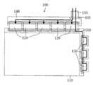
図8は、ゲートドライバIC用のPCBを省いた液晶表示装置を模式的に示す平面図である。図8に示す液晶表示装置100は、液晶パネル110と、液晶パネル110の端部で接続されたソースCOF120およびゲートCOF130と、ソースCOF120に接続されたソースPCB140と、ソースPCB140に接続された入力用FPC150とを備える。液晶表示装置100にはゲートPCBがないので、ゲートCOF130に搭載されたドライバICへのゲート信号や電源電圧は、入力用FPC150、ソースPCB140、ソースCOF120、パネル側配線160を順次経て入力される。したがって、ソースCOF120は、ドライバICへソース信号を入力するための配線やドライバICから液晶パネル110へ出力するための配線だけでなく、ゲート信号を中継するための配線を有する。 FIG. 8 is a plan view schematically showing a liquid crystal display device in which the PCB for the gate driver IC is omitted. The liquid
現状の製造設備では、液晶パネル110の端部に配置される複数のソースCOF120のうち1つだけサイズの異なるソースCOFを用いるのは困難であり、同じサイズのソースCOF120を用いる必要がある。したがって、すべてのソースCOF120が中継配線を有するので、中継配線のないソースCOFと比べてサイズが大きくなるだけでなく、コスト高となる。 In the current manufacturing facility, it is difficult to use only one
また、典型的には、入力用FPC150はコネクタ141を介してソースPCB140に接続されるので、部材点数が増え、コスト高になる。さらに、手作業により接続する必要があるので、作業工数を削減することが困難であり、製造効率が良くない。コストや製造効率を考慮して、入力用FPC150をソースPCB140に半田付けすることも可能である。しかし、近年の鉛フリーの社会要請に反し、環境の点で問題がある。
本発明の目的の1つは、作業工数を削減して、製造効率を高めることである。本発明の他の目的は、部材点数を削減して、コストダウンを図ることである。 One of the objects of the present invention is to reduce the number of work steps and increase the production efficiency. Another object of the present invention is to reduce costs by reducing the number of members.
本発明の第1の局面による入力用配線フィルムは、フィルム基材と、前記フィルム基材に形成され、表示装置に信号を入力するための入力用配線とを有する。前記表示装置は、第1信号配線を有する表示パネルと、前記第1信号配線に接続され、前記第1信号配線への信号の出力を制御する第1回路を有する第1回路フィルムと、前記第1回路フィルムに接続され、前記第1回路に信号を入力するための第1回路用配線を有する配線基板とを備える。前記フィルム基材は、前記配線基板に接続される領域と、前記表示パネルに接続される領域とを有する。前記入力用配線は前記第1回路用配線に信号を入力するための第1入力用配線を少なくとも含み、前記フィルム基材と前記配線基板とが接続されることによって、前記第1入力用配線が前記第1回路用配線と接続される。 The input wiring film according to the first aspect of the present invention includes a film base and an input wiring formed on the film base for inputting a signal to the display device. The display device includes a display panel having a first signal wiring, a first circuit film connected to the first signal wiring and having a first circuit that controls output of a signal to the first signal wiring, A wiring board connected to a one-circuit film and having a first circuit wiring for inputting a signal to the first circuit. The film base has an area connected to the wiring board and an area connected to the display panel. The input wiring includes at least a first input wiring for inputting a signal to the first circuit wiring, and the first input wiring is connected by connecting the film base and the wiring substrate. Connected to the first circuit wiring.
本発明の第1の局面による入力用配線フィルムは、配線基板に接続される領域を有するので、第1回路フィルムと配線基板との接続と同時に、配線基板に接続することができる。これにより、入力用配線フィルムの第1入力用配線が配線基板の第1回路用配線と接続されるので、第1回路用配線を介して、入力用配線フィルムから第1回路フィルムの第1回路へ信号を入力することができる。また入力用配線フィルムは、表示パネルに接続される領域を有するので、第1回路フィルムと表示パネルとの接続と同時に、表示パネルに接続することができる。したがって、本発明の第1の局面による入力用配線フィルムによれば、作業工数が削減され、製造効率が高められる。またコネクタを用いずに、入力用配線フィルムを配線基板に接続することができるので、部材点数が削減され、コストダウンが図られる。 Since the input wiring film according to the first aspect of the present invention has a region connected to the wiring board, it can be connected to the wiring board simultaneously with the connection of the first circuit film and the wiring board. As a result, the first input wiring of the input wiring film is connected to the first circuit wiring of the wiring substrate, so that the first circuit of the first circuit film is connected from the input wiring film via the first circuit wiring. A signal can be input. Moreover, since the wiring film for input has the area | region connected to a display panel, it can connect to a display panel simultaneously with the connection of a 1st circuit film and a display panel. Therefore, according to the input wiring film according to the first aspect of the present invention, the number of work steps is reduced and the manufacturing efficiency is increased. Further, since the input wiring film can be connected to the wiring board without using a connector, the number of members can be reduced and the cost can be reduced.
本発明の第2の局面による入力用配線フィルムは、フィルム基材と、前記フィルム基材に形成され、表示装置に信号を入力するための入力用配線とを有する。前記表示装置は、第1信号配線および第2信号配線を有する表示パネルと、前記第1信号配線に接続され、前記第1信号配線への信号の出力を制御する第1回路を有する第1回路フィルムと、前記第1回路フィルムに接続され、前記第1回路へ信号を入力するための第1回路用配線を有する配線基板と、前記第2信号配線に接続され、前記第2信号配線への信号の出力を制御する第2回路を有する第2回路フィルムとを備え、前記表示パネルが前記第2回路へ信号を入力するための第2回路用配線を有する。前記フィルム基材は、前記配線基板に接続される領域と、前記表示パネルに接続される領域とを有する。前記入力用配線は、前記第1回路用配線に信号を入力するための第1入力用配線と、前記第2回路用配線に信号を入力するための第2入力用配線とを含み、前記フィルム基材と前記配線基板とが接続されることによって、前記第1入力用配線が前記第1回路用配線と接続され、前記フィルム基材と前記表示パネルとが接続されることによって、前記第2入力用配線が前記第2回路用配線と接続される。 An input wiring film according to a second aspect of the present invention includes a film base and an input wiring formed on the film base for inputting a signal to a display device. The display device includes a display panel having a first signal wiring and a second signal wiring, and a first circuit having a first circuit connected to the first signal wiring and controlling output of a signal to the first signal wiring. A film, a wiring board connected to the first circuit film and having a first circuit wiring for inputting a signal to the first circuit, and connected to the second signal wiring, to the second signal wiring; And a second circuit film having a second circuit for controlling signal output, and the display panel has a second circuit wiring for inputting a signal to the second circuit. The film base has an area connected to the wiring board and an area connected to the display panel. The input wiring includes a first input wiring for inputting a signal to the first circuit wiring and a second input wiring for inputting a signal to the second circuit wiring, and the film By connecting the base material and the wiring substrate, the first input wiring is connected to the first circuit wiring, and the film base material and the display panel are connected to each other. The input wiring is connected to the second circuit wiring.
本発明の第2の局面による入力用配線フィルムは、配線基板に接続される領域を有するので、第1回路フィルムと配線基板との接続と同時に、配線基板に接続することができる。これにより、入力用配線フィルムの第1入力用配線が配線基板の第1回路用配線と接続されるので、第1回路用配線を介して、入力用配線フィルムから第1回路フィルムの第1回路へ信号を入力することができる。また入力用配線フィルムは、表示パネルに接続される領域を有するので、第1回路フィルムと表示パネルとの接続と同時に、表示パネルに接続することができる。これにより、入力用配線フィルムの第2入力用配線が表示パネルの第2回路用配線と接続されるので、第2回路用配線を介して、入力用配線フィルムから第2回路フィルムの第2回路へ信号を入力することができる。したがって、本発明の第2の局面による入力用配線フィルムによれば、作業工数が削減され、製造効率が高められる。 Since the input wiring film according to the second aspect of the present invention has a region to be connected to the wiring board, it can be connected to the wiring board simultaneously with the connection of the first circuit film and the wiring board. As a result, the first input wiring of the input wiring film is connected to the first circuit wiring of the wiring substrate, so that the first circuit of the first circuit film is connected from the input wiring film via the first circuit wiring. A signal can be input. Moreover, since the wiring film for input has the area | region connected to a display panel, it can connect to a display panel simultaneously with the connection of a 1st circuit film and a display panel. As a result, the second input wiring of the input wiring film is connected to the second circuit wiring of the display panel, so that the second circuit of the second circuit film is connected from the input wiring film via the second circuit wiring. A signal can be input. Therefore, according to the input wiring film according to the second aspect of the present invention, the number of work steps is reduced, and the manufacturing efficiency is increased.
また本発明の第2の局面による入力用配線フィルムは、第2回路用配線に信号を入力するための第2入力用配線を含むので、第1回路フィルムに第2回路用配線に信号を入力するための配線を形成する必要がない。したがって、第1回路フィルムのサイズを小さくすることができ、コストダウンが可能となる。 Further, the input wiring film according to the second aspect of the present invention includes a second input wiring for inputting a signal to the second circuit wiring, so that a signal is input to the second circuit wiring to the first circuit film. There is no need to form wiring for the purpose. Therefore, the size of the first circuit film can be reduced, and the cost can be reduced.
本発明の第3の局面による入力用配線フィルムは、フィルム基材と、前記フィルム基材に形成され、表示装置に信号を入力するための入力用配線とを有する。前記表示装置は、第1信号配線および第2信号配線を有する表示パネルと、前記第1信号配線に接続され、前記第1信号配線への信号の出力を制御する第1回路を有する第1回路フィルムと、前記第1回路フィルムに接続され、前記第1回路へ信号を入力するための第1回路用配線を有する配線基板と、前記第2信号配線に接続され、前記第2信号配線への信号の出力を制御する第2回路を有する第2回路フィルムとを備え、前記表示パネルが前記第1回路へ信号を入力するための第1回路用パネル側配線と、前記第2回路へ信号を入力するための第2回路用配線とを有する。前記フィルム基材は、前記配線基板に接続される領域と、前記表示パネルに接続される領域とを有する。前記入力用配線は、前記第1回路用配線に信号を入力するための第1入力用配線と、前記第2回路用配線に信号を入力するための第2入力用配線と、前記第1回路用パネル側配線に信号を入力するための第3入力用配線とを含み、前記フィルム基材と前記配線基板とが接続されることによって、前記第1入力用配線が前記第1回路用配線と接続され、前記フィルム基材と前記表示パネルとが接続されることによって、前記第2入力用配線が前記第2回路用配線と接続されるとともに、前記第3入力用配線が前記第1回路用パネル側配線と接続される。 An input wiring film according to a third aspect of the present invention has a film base and an input wiring formed on the film base for inputting a signal to a display device. The display device includes a display panel having a first signal wiring and a second signal wiring, and a first circuit having a first circuit connected to the first signal wiring and controlling output of a signal to the first signal wiring. A film, a wiring board connected to the first circuit film and having a first circuit wiring for inputting a signal to the first circuit, and connected to the second signal wiring, to the second signal wiring; A second circuit film having a second circuit for controlling the output of the signal, the panel-side wiring for the first circuit for the display panel to input the signal to the first circuit, and the signal to the second circuit And a second circuit wiring for input. The film base has an area connected to the wiring board and an area connected to the display panel. The input wiring includes a first input wiring for inputting a signal to the first circuit wiring, a second input wiring for inputting a signal to the second circuit wiring, and the first circuit. A third input wiring for inputting a signal to the panel-side wiring, and the first input wiring is connected to the first circuit wiring by connecting the film base and the wiring substrate. When the film substrate and the display panel are connected, the second input wiring is connected to the second circuit wiring, and the third input wiring is used for the first circuit. Connected to panel side wiring.
本発明の第3の局面による入力用配線フィルムは、本発明の第2の局面による入力用配線フィルムの作用効果に加えて、以下の作用効果を有する。本発明の第3の局面による入力用配線フィルムは、第1回路用パネル側配線に信号を入力するための第3入力用配線を有するので、入力用配線フィルムと表示パネルとが接続されることによって、第3入力用配線が第1回路用パネル側配線と接続される。これにより、表示パネル上の配線を経由して、入力用配線フィルムから第1回路フィルムの第1回路に信号を入力することができる。したがって、配線基板上の配線数が減少するので、配線基板サイズの縮小化が可能となり、配線基板のコストを削減することができる。 The input wiring film according to the third aspect of the present invention has the following operational effects in addition to the operational effects of the input wiring film according to the second aspect of the present invention. Since the input wiring film according to the third aspect of the present invention has the third input wiring for inputting a signal to the first circuit panel side wiring, the input wiring film and the display panel are connected. Thus, the third input wiring is connected to the first circuit panel side wiring. Accordingly, a signal can be input from the input wiring film to the first circuit of the first circuit film via the wiring on the display panel. Accordingly, since the number of wirings on the wiring board is reduced, the size of the wiring board can be reduced, and the cost of the wiring board can be reduced.
また、配線基板上の端子数が削減されるので、端子のピッチを大きくすることができ、第1回路フィルムとの接続が容易となる。したがって、良品率が向上し、配線基板の長尺化が可能となる。 Moreover, since the number of terminals on the wiring board is reduced, the pitch of the terminals can be increased, and the connection with the first circuit film is facilitated. Therefore, the yield rate is improved and the wiring board can be made longer.
本発明の第4の局面による入力用配線フィルムは、フィルム基材と、前記フィルム基材に形成され、表示装置に信号を入力するための入力用配線とを有する。前記表示装置は、複数の第1信号配線を有する表示パネルと、前記複数の第1信号配線のうちの少なくとも1つの第1信号配線に接続され、前記少なくとも1つの第1信号配線への信号の出力を制御する第1回路をそれぞれ有する複数の第1回路フィルムと、前記複数の第1回路フィルムのうちの少なくとも1つの第1回路フィルムにそれぞれ接続され、前記少なくとも1つの第1回路へ信号を入力するための第1回路用配線をそれぞれ有する第1および第2配線基板とを備える。前記フィルム基材は、前記第1および第2配線基板にそれぞれ接続される領域と、前記表示パネルに接続される領域とを有する。前記入力用配線は、前記第1配線基板の第1回路用配線と、前記第2配線基板の第1回路用配線とを中継する中継配線を含み、前記フィルム基材と前記第1および第2配線基板とが接続されることによって、前記第1配線基板の第1回路用配線と前記第2配線基板の第1回路用配線とが前記中継配線を介して接続される。 An input wiring film according to a fourth aspect of the present invention includes a film base and an input wiring formed on the film base for inputting a signal to a display device. The display device is connected to a display panel having a plurality of first signal wirings and at least one first signal wiring of the plurality of first signal wirings, and a signal to the at least one first signal wiring is transmitted. A plurality of first circuit films each having a first circuit for controlling an output, and each of the plurality of first circuit films is connected to at least one first circuit film, and a signal is transmitted to the at least one first circuit. First and second wiring boards each having a first circuit wiring for input. The film base has a region connected to the first and second wiring boards and a region connected to the display panel. The input wiring includes a relay wiring that relays the first circuit wiring of the first wiring board and the first circuit wiring of the second wiring board, and includes the film base and the first and second wirings. When the wiring board is connected, the first circuit wiring of the first wiring board and the first circuit wiring of the second wiring board are connected via the relay wiring.
一般に、表示パネルの大型化に伴って、複数の配線基板が用いられ、各配線基板に入力FPCがそれぞれ接続される。本発明の第4の局面による入力用配線フィルムは、第1配線基板の第1回路用配線と第2配線基板の第1回路用配線とを中継する中継配線を有するので、第2配線基板に入力FPCを接続することなく、第2配線基板に接続された第1回路フィルムの第1回路に信号を入力することができる。したがって、作業工数が削減され、製造効率が高められる。またコネクタを用いずに、第2配線基板に接続された第1回路フィルムの第1回路に信号を入力することができるので、部材点数が削減され、コストダウンが図られる。 In general, as the display panel is increased in size, a plurality of wiring boards are used, and an input FPC is connected to each wiring board. The input wiring film according to the fourth aspect of the present invention has a relay wiring that relays the first circuit wiring of the first wiring board and the first circuit wiring of the second wiring board. A signal can be input to the first circuit of the first circuit film connected to the second wiring board without connecting the input FPC. Therefore, the number of work steps is reduced and the production efficiency is increased. Further, since a signal can be input to the first circuit of the first circuit film connected to the second wiring board without using a connector, the number of members is reduced and the cost is reduced.
また本発明の第4の局面による入力用配線フィルムは、第1および第2配線基板にそれぞれ接続される領域を有するので、第1回路フィルムと第1および第2配線基板との接続と同時に、第1および第2配線基板に接続することができる。また入力用配線フィルムは、表示パネルに接続される領域を有するので、第1回路フィルムと表示パネルとの接続と同時に、表示パネルに接続することができる。したがって、本発明の第4の局面による入力用配線フィルムによれば、作業工数が削減され、製造効率が高められる。 In addition, since the input wiring film according to the fourth aspect of the present invention has regions connected to the first and second wiring boards, simultaneously with the connection between the first circuit film and the first and second wiring boards, It can be connected to the first and second wiring boards. Moreover, since the wiring film for input has the area | region connected to a display panel, it can connect to a display panel simultaneously with the connection of a 1st circuit film and a display panel. Therefore, according to the input wiring film of the fourth aspect of the present invention, the number of work steps is reduced and the manufacturing efficiency is increased.
本発明の第5の局面による入力用配線フィルムは、フィルム基材と、前記フィルム基材に形成され、表示装置に信号を入力するための入力用配線とを有する。前記表示装置は、複数の第1信号配線と第2信号配線とを有する表示パネルと、前記複数の第1信号配線のうちの少なくとも1つの第1信号配線に接続され、前記少なくとも1つの第1信号配線への信号の出力を制御する第1回路をそれぞれ有する複数の第1回路フィルムと、前記複数の第1回路フィルムのうちの少なくとも1つの第1回路フィルムにそれぞれ接続され、前記少なくとも1つの第1回路へ信号を入力するための第1回路用配線をそれぞれ有する第1および第2配線基板と、前記第2信号配線に接続され、前記第2信号配線への信号の出力を制御する第2回路を有する第2回路フィルムとを備え、前記第1配線基板は前記第2回路へ信号を入力するための第2回路用配線を有する。前記フィルム基材は、前記第1および第2配線基板にそれぞれ接続される領域と、前記表示パネルに接続される領域とを有する。前記入力用配線は、前記第1配線基板の前記第1回路用配線に信号を入力するための第1配線基板用配線と、前記第2配線基板の前記第1回路用配線に信号を入力するための第2配線基板用配線と、前記第2回路用配線に信号を入力するための第2入力用配線とを含み、前記フィルム基材と前記第1および第2配線基板とが接続されることによって、前記第1配線基板用配線が前記第1配線基板の前記第1回路用配線と接続され、前記第2配線基板用配線が前記第2配線基板の前記第1回路用配線と接続されるとともに、前記第2入力用配線が前記第2回路用配線と接続される。 An input wiring film according to a fifth aspect of the present invention includes a film base and an input wiring formed on the film base for inputting a signal to a display device. The display device is connected to a display panel having a plurality of first signal lines and a second signal line, and to at least one first signal line of the plurality of first signal lines, and the at least one first signal line. A plurality of first circuit films each having a first circuit for controlling output of a signal to the signal wiring; and at least one first circuit film of the plurality of first circuit films, respectively, First and second wiring boards each having a first circuit wiring for inputting a signal to the first circuit, and a second circuit connected to the second signal wiring and controlling the output of the signal to the second signal wiring. A second circuit film having two circuits, and the first wiring board has a second circuit wiring for inputting a signal to the second circuit. The film base has a region connected to the first and second wiring boards and a region connected to the display panel. The input wiring inputs a signal to the first wiring board wiring for inputting a signal to the first circuit wiring of the first wiring board and the first circuit wiring of the second wiring board. And a second input wiring for inputting a signal to the second circuit wiring, and the film base and the first and second wiring boards are connected to each other. Accordingly, the first wiring board wiring is connected to the first circuit wiring of the first wiring board, and the second wiring board wiring is connected to the first circuit wiring of the second wiring board. In addition, the second input wiring is connected to the second circuit wiring.
本発明の第5の局面による入力用配線フィルムは、第1および第2配線基板にそれぞれ接続される領域を有するので、第1回路フィルムと第1および第2配線基板との接続と同時に、第1および第2配線基板に接続することができる。これにより、入力用配線フィルムの第1配線基板用配線が第1配線基板の第1回路用配線と接続されるので、第1配線基板の第1回路用配線を介して、第1配線基板に接続された第1回路フィルムの第1回路へ信号を入力することができる。また入力用配線フィルムの第2配線基板用配線が第2配線基板の第1回路用配線と接続されるので、第2配線基板の第1回路用配線を介して、第2配線基板に接続された第1回路フィルムの第1回路へ信号を入力することができる。すなわち、第1および第2配線基板のそれぞれに入力FPCを接続することなく、第1および第2配線基板に接続された第1回路フィルムの第1回路に信号を入力することができる。したがって、作業工数が削減され、製造効率が高められる。またコネクタを用いずに、各配線基板に接続された第1回路フィルムの第1回路に信号を入力することができるので、部材点数が削減され、コストダウンが図られる。 Since the input wiring film according to the fifth aspect of the present invention has regions connected to the first and second wiring boards, respectively, the first circuit film and the first and second wiring boards are connected simultaneously with the first circuit film. The first and second wiring boards can be connected. As a result, the first wiring board wiring of the input wiring film is connected to the first circuit wiring of the first wiring board, so that the first wiring board is connected to the first wiring board via the first circuit wiring of the first wiring board. A signal can be input to the first circuit of the connected first circuit film. Also, since the second wiring board wiring of the input wiring film is connected to the first circuit wiring of the second wiring board, it is connected to the second wiring board via the first circuit wiring of the second wiring board. A signal can be input to the first circuit of the first circuit film. That is, a signal can be input to the first circuit of the first circuit film connected to the first and second wiring boards without connecting the input FPC to each of the first and second wiring boards. Therefore, the number of work steps is reduced and the production efficiency is increased. Moreover, since a signal can be input to the first circuit of the first circuit film connected to each wiring board without using a connector, the number of members is reduced and the cost is reduced.
本発明の第1の局面による表示装置は、第1信号配線を有する表示パネルと、前記第1信号配線に接続され、前記第1信号配線への信号の出力を制御する第1回路を有する第1回路フィルムと、前記第1回路フィルムに接続され、前記第1回路に信号を入力するための第1回路用配線を有する配線基板と、入力用配線フィルムとを備える。前記入力用配線フィルムは、フィルム基材と、前記フィルム基材に形成され、前記第1回路用配線に信号を入力するための第1入力用配線とを有する。前記フィルム基材は前記配線基板に接続されるとともに、前記表示パネルに接続され、前記フィルム基材と前記配線基板とが接続されることによって、前記第1入力用配線が前記第1回路用配線と接続されている。 A display device according to a first aspect of the present invention includes a display panel having a first signal line, and a first circuit that is connected to the first signal line and controls output of a signal to the first signal line. A circuit board, a wiring board connected to the first circuit film and having a first circuit wiring for inputting a signal to the first circuit, and an input wiring film are provided. The input wiring film has a film base material and a first input wiring formed on the film base material for inputting a signal to the first circuit wiring. The film base is connected to the wiring board, is connected to the display panel, and the film base and the wiring board are connected, whereby the first input wiring is connected to the first circuit wiring. Connected with.
本発明の第2の局面による表示装置は、第1信号配線および第2信号配線を有する表示パネルと、前記第1信号配線に接続され、前記第1信号配線への信号の出力を制御する第1回路を有する第1回路フィルムと、前記第1回路フィルムに接続され、前記第1回路へ信号を入力するための第1回路用配線を有する配線基板と、前記第2信号配線に接続され、前記第2信号配線への信号の出力を制御する第2回路を有する第2回路フィルムと、入力用配線フィルムとを備え、前記表示パネルが前記第2回路へ信号を入力するための第2回路用配線を有する。前記入力用配線フィルムは、フィルム基材と、前記フィルム基材に形成された入力用配線とを有する。前記入力用配線は、前記第1回路用配線に信号を入力するための第1入力用配線と、前記第2回路用配線に信号を入力するための第2入力用配線とを含み、前記フィルム基材は前記配線基板に接続されるとともに、前記表示パネルに接続され、前記フィルム基材と前記配線基板とが接続されることによって、前記第1入力用配線が前記第1回路用配線と接続され、前記フィルム基材と前記表示パネルとが接続されることによって、前記第2入力用配線が前記第2回路用配線と接続されている。 A display device according to a second aspect of the present invention includes a display panel having a first signal line and a second signal line, and a first panel connected to the first signal line and controlling the output of a signal to the first signal line. A first circuit film having one circuit, a wiring board connected to the first circuit film and having a first circuit wiring for inputting a signal to the first circuit, and connected to the second signal wiring; A second circuit having a second circuit film having a second circuit for controlling the output of a signal to the second signal wiring; and an input wiring film, wherein the display panel inputs a signal to the second circuit. Wiring. The input wiring film has a film base and input wiring formed on the film base. The input wiring includes a first input wiring for inputting a signal to the first circuit wiring and a second input wiring for inputting a signal to the second circuit wiring, and the film The base material is connected to the wiring board, is connected to the display panel, and the film base material and the wiring board are connected, whereby the first input wiring is connected to the first circuit wiring. And the said 2nd input wiring is connected with the said 2nd circuit wiring by connecting the said film base material and the said display panel.
本発明の第3の局面による表示装置は、第1信号配線および第2信号配線を有する表示パネルと、前記第1信号配線に接続され、前記第1信号配線への信号の出力を制御する第1回路を有する第1回路フィルムと、前記第1回路フィルムに接続され、前記第1回路へ信号を入力するための第1回路用配線を有する配線基板と、前記第2信号配線に接続され、前記第2信号配線への信号の出力を制御する第2回路を有する第2回路フィルムと、入力用配線フィルムとを備え、前記表示パネルが前記第1回路へ信号を入力するための第1回路用パネル側配線と、前記第2回路へ信号を入力するための第2回路用配線とを有する。前記入力用配線フィルムは、フィルム基材と、前記フィルム基材に形成された入力用配線とを有する。前記入力用配線は、前記第1回路用配線に信号を入力するための第1入力用配線と、前記第2回路用配線に信号を入力するための第2入力用配線と、前記第1回路用パネル側配線に信号を入力するための第3入力用配線とを含み、前記フィルム基材は前記配線基板に接続されるとともに、前記表示パネルに接続され、前記フィルム基材と前記配線基板とが接続されることによって、前記第1入力用配線が前記第1回路用配線と接続され、前記フィルム基材と前記表示パネルとが接続されることによって、前記第2入力用配線が前記第2回路用配線と接続されるとともに、前記第3入力用配線が前記第1回路用パネル側配線と接続されている。 A display device according to a third aspect of the present invention includes a display panel having a first signal line and a second signal line, and a first panel connected to the first signal line and controlling the output of a signal to the first signal line. A first circuit film having one circuit, a wiring board connected to the first circuit film and having a first circuit wiring for inputting a signal to the first circuit, and connected to the second signal wiring; A first circuit for inputting a signal to the first circuit, the second circuit film having a second circuit for controlling output of a signal to the second signal wiring, and an input wiring film; Panel side wiring and second circuit wiring for inputting a signal to the second circuit. The input wiring film has a film base and input wiring formed on the film base. The input wiring includes a first input wiring for inputting a signal to the first circuit wiring, a second input wiring for inputting a signal to the second circuit wiring, and the first circuit. A third input wiring for inputting a signal to the panel-side wiring, and the film base is connected to the wiring board and connected to the display panel, and the film base and the wiring board Is connected, the first input wiring is connected to the first circuit wiring, and the film base and the display panel are connected, so that the second input wiring is the second wiring. The third input wiring is connected to the first circuit panel side wiring while being connected to the circuit wiring.
本発明の第4の局面による表示装置は、複数の第1信号配線を有する表示パネルと、前記複数の第1信号配線のうちの少なくとも1つの第1信号配線に接続され、前記少なくとも1つの第1信号配線への信号の出力を制御する第1回路をそれぞれ有する複数の第1回路フィルムと、前記複数の第1回路フィルムのうちの少なくとも1つの第1回路フィルムにそれぞれ接続され、前記少なくとも1つの第1回路へ信号を入力するための第1回路用配線をそれぞれ有する第1および第2配線基板と、入力用配線フィルムとを備える。前記入力用配線フィルムは、フィルム基材と、前記フィルム基材に形成された入力用配線とを有する。前記入力用配線は、前記第1配線基板の第1回路用配線と、前記第2配線基板の第1回路用配線とを中継する中継配線を含み、前記フィルム基材は、前記第1および第2配線基板にそれぞれ接続されるとともに、前記表示パネルに接続され、前記フィルム基材と前記第1および第2配線基板とが接続されることによって、前記第1配線基板の第1回路用配線と前記第2配線基板の第1回路用配線とが前記中継配線を介して接続されている。 A display device according to a fourth aspect of the present invention is connected to a display panel having a plurality of first signal lines and at least one first signal line of the plurality of first signal lines, and the at least one first signal line. A plurality of first circuit films each having a first circuit for controlling output of a signal to one signal wiring; and at least one first circuit film of the plurality of first circuit films, respectively, First and second wiring boards each having a first circuit wiring for inputting signals to two first circuits, and an input wiring film are provided. The input wiring film has a film base and input wiring formed on the film base. The input wiring includes a relay wiring that relays the first circuit wiring of the first wiring board and the first circuit wiring of the second wiring board, and the film base includes the first and first wirings. The first circuit wiring of the first wiring board is connected to the two wiring boards, connected to the display panel, and connected to the film base and the first and second wiring boards. The first circuit wiring of the second wiring board is connected via the relay wiring.
本発明の第5の局面による表示装置は、複数の第1信号配線と第2信号配線とを有する表示パネルと、前記複数の第1信号配線のうちの少なくとも1つの第1信号配線に接続され、前記少なくとも1つの第1信号配線への信号の出力を制御する第1回路をそれぞれ有する複数の第1回路フィルムと、前記複数の第1回路フィルムのうちの少なくとも1つの第1回路フィルムにそれぞれ接続され、前記少なくとも1つの第1回路へ信号を入力するための第1回路用配線をそれぞれ有する第1および第2配線基板と、前記第2信号配線に接続され、前記第2信号配線への信号の出力を制御する第2回路を有する第2回路フィルムと、入力用配線フィルムとを備え、前記第1配線基板は前記第2回路へ信号を入力するための第2回路用配線を有する。前記入力用配線フィルムは、フィルム基材と、前記フィルム基材に形成された入力用配線とを有する。前記入力用配線は、前記第1配線基板の前記第1回路用配線に信号を入力するための第1配線基板用配線と、前記第2配線基板の前記第1回路用配線に信号を入力するための第2配線基板用配線と、前記第2回路用配線に信号を入力するための第2入力用配線とを含み、前記フィルム基材は、前記第1および第2配線基板にそれぞれ接続されるとともに、前記表示パネルに接続され、前記フィルム基材と前記第1および第2配線基板とが接続されることによって、前記第1配線基板用配線が前記第1配線基板の前記第1回路用配線と接続され、前記第2配線基板用配線が前記第2配線基板の前記第1回路用配線と接続されるとともに、前記第2入力用配線が前記第2回路用配線と接続されている。 A display device according to a fifth aspect of the present invention is connected to a display panel having a plurality of first signal lines and a second signal line, and at least one first signal line among the plurality of first signal lines. A plurality of first circuit films each having a first circuit for controlling output of a signal to the at least one first signal wiring, and at least one first circuit film of the plurality of first circuit films, respectively. First and second wiring boards connected to each other and having a first circuit wiring for inputting a signal to the at least one first circuit, and connected to the second signal wiring, A second circuit film having a second circuit for controlling signal output; and an input wiring film, wherein the first wiring board has a second circuit wiring for inputting a signal to the second circuit.The input wiring film has a film base and input wiring formed on the film base. The input wiring inputs a signal to the first wiring board wiring for inputting a signal to the first circuit wiring of the first wiring board and the first circuit wiring of the second wiring board. Second wiring board wiring for input and second input wiring for inputting a signal to the second circuit wiring, and the film base is connected to the first and second wiring boards, respectively. In addition, the first wiring board wiring is connected to the display panel, and the film base and the first and second wiring boards are connected, whereby the first wiring board wiring is used for the first circuit of the first wiring board. The second wiring board wiring is connected to the first circuit wiring of the second wiring board, and the second input wiring is connected to the second circuit wiring.
本発明の第1〜第3の局面による表示装置において、前記フィルム基材と前記配線基板との接続および前記フィルム基材と前記表示パネルとの接続が異方性導電膜を介してそれぞれ行われていることが好ましい。 In the display device according to the first to third aspects of the present invention, the connection between the film base and the wiring board and the connection between the film base and the display panel are performed via an anisotropic conductive film, respectively. It is preferable.
本発明の第4および第5の局面による表示装置において、前記フィルム基材と前記第1および第2配線基板との接続および前記フィルム基材と前記表示パネルとの接続が異方性導電膜を介してそれぞれ行われていることが好ましい。 In the display device according to the fourth and fifth aspects of the present invention, the connection between the film base and the first and second wiring boards and the connection between the film base and the display panel are anisotropic conductive films. It is preferable that each of them is performed.
本発明によれば、作業工数を削減して、製造効率を高めることができる。また部材点数を削減して、コストダウンを図ることができる。 According to the present invention, the number of work steps can be reduced and the production efficiency can be increased. Further, the number of members can be reduced, and the cost can be reduced.
以下、図面を参照しながら本発明の実施形態を説明する。以下の実施形態では、表示装置の例として、液晶パネルを備えた液晶表示装置について説明する。しかし、本発明の表示装置は、液晶表示装置に限定されない。例えば、無機または有機EL(Electro Luminescence)表示装置であっても良い。なお、液晶表示装置は、透過型、反射型、反射透過両用型のいずれのタイプでも良い。また、本明細書における「信号」は電源電圧を含むことがある。 Hereinafter, embodiments of the present invention will be described with reference to the drawings. In the following embodiments, a liquid crystal display device including a liquid crystal panel will be described as an example of the display device. However, the display device of the present invention is not limited to a liquid crystal display device. For example, an inorganic or organic EL (Electro Luminescence) display device may be used. The liquid crystal display device may be any of a transmission type, a reflection type, and a reflection / transmission type. In addition, the “signal” in this specification may include a power supply voltage.
(実施形態1)
本実施形態は、本発明の第2の局面による入力用配線フィルムおよび表示装置の実施形態である。図1は実施形態1の液晶表示装置1を模式的に示す平面図であり、図2は図1中の破線で囲まれた部分Aの拡大図である。(Embodiment 1)
This embodiment is an embodiment of an input wiring film and a display device according to the second aspect of the present invention. FIG. 1 is a plan view schematically showing the liquid crystal display device 1 of Embodiment 1, and FIG. 2 is an enlarged view of a portion A surrounded by a broken line in FIG.
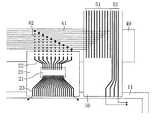
液晶表示装置1は、液晶パネル10と、液晶パネル10の周縁部にて接続された複数のソースCOF20と、液晶パネル10の周縁部にて接続された複数のゲートCOF30と、複数のソースCOF20に接続されたソースPCB40と、液晶パネル10およびソースPCB40に接続された入力用FPC50とを備える。なお、図1では、ソースCOF20が5枚、ゲートCOF30が3枚であるが、これらの枚数について制限はない。 The liquid crystal display device 1 includes a
液晶パネル10は、TFT(Thin Film Transistor)基板11と、TFT基板11に対向配置されたカラーフィルタ基板12と、両基板11,12間に介在する液晶層(不図示)とを有する。TFT基板11は、それぞれが互いに平行で列方向に延びる複数のソース配線と、複数のソース配線とそれぞれ交差し、かつそれぞれが互いに平行に延びる複数のゲート配線と、ソース配線およびゲート配線と電気的に接続され、マトリクス状に配置されたTFTと、TFTを介してソース配線と接続された画素電極とを有する。TFT基板11の周縁部にはソース配線およびゲート配線の各端子が形成されている。カラーフィルタ基板12は、赤、緑、青の各色のカラーフィルタと、カラーフィルタを覆う共通電極とを有する。TFT基板11およびカラーフィルタ基板12それぞれの液晶層側には、配向膜が形成され、ラビング処理が施されている。 The
ソースCOF20およびゲートCOF30は、ガラスやポリイミド系樹脂等からなるフィルム基材と、フィルム基材上に搭載されたドライバICと、フィルム基材に形成された銅箔等の配線パターンとを有する。配線パターンは、複数本の配線から構成され、プレーティング法またはキャスティング法により形成される。なお、ソースCOF20およびゲートCOF30には、ドライバICだけでなく、その他各種部品が搭載されることがある。 The source COF 20 and the
図2に示すように、ソースCOF20は、ソースドライバIC21へ信号を入力するための入力配線22と、ソースドライバIC21から液晶パネル10のソース配線へ信号を出力するための出力配線23とを有する。一方、ゲートCOF30は、ゲートドライバICへ信号を入力するための入力配線と、ゲートドライバICから液晶パネル10のゲート配線へ信号を出力するための出力配線と、隣接するゲートCOF30へ信号を順次伝播させるための中継配線とを有する。液晶パネル10のゲートCOF30側周縁部には、ゲートドライバICへ信号を入力するためのゲートドライバIC用配線13と、隣接するゲートCOF30へ信号を順次伝播させるためのパネル側中継配線(不図示)とが形成されている。 As shown in FIG. 2, the
ソースPCB40は、入力用FPC50からソースドライバIC21へ信号を入力するためのソースドライバ用配線41を有する。ソースドライバ用配線41は、ソースPCB40の長手方向に延びており、長手方向に対して交差する方向に延びた取り出し配線42に接続されている。ソースPCB40は、液晶制御回路や外部インターフェース回路(いずれも不図示)をさらに有する。 The
入力用FPC50は、ガラスやポリイミド系樹脂等からなるフィルム基材と、フィルム基材に形成された銅箔等の配線パターンとを有する。配線パターンは、ソースドライバIC21へ信号を入力するためのソース入力用配線51と、ゲートドライバICへ信号を入力するためのゲート入力用配線52とを含む。 The
ソースCOF20およびゲートCOF30は、液晶パネル10の周縁部に形成された、ソース配線およびゲート配線の各端子と、異方性導電膜61,62を介して、熱圧着により接続されている。また入力用FPC50の端部も異方性導電膜61を介して液晶パネル10の周縁部に接続されている。これにより、ソースCOF20の出力配線23が液晶パネル10のソース配線の端子に接続され、ゲートCOF30の出力配線が液晶パネル10のゲート配線の端子に接続される。また入力用FPC50のゲート入力用配線52が、液晶パネル10に形成されたゲートドライバIC用配線13に接続される。 The source COF 20 and the
さらに、ソースCOF20および入力用FPC50は、異方性導電膜63を介して、ソースPCB40と接続されている。これにより、ソースCOF20の入力配線22とソースPCB40の取り出し配線42とが接続され、入力用FPC50のソース入力用配線51とソースPCB40のソースドライバ用配線41とが接続される。 Further, the source COF 20 and the
次に、液晶表示装置1上を伝播する信号の伝達経路について説明する。図示しないコントロール基板から出力されたソース信号は、入力用FPC50のソース入力用配線51、ソースPCB40のソースドライバ用配線41および取り出し配線42を介して、ソースCOF20の入力配線22に入力される。入力信号に従って、ソースドライバIC21から出力配線23に信号が出力され、液晶パネル10のソース配線に信号が入力される。 Next, a transmission path of a signal propagating on the liquid crystal display device 1 will be described. A source signal output from a control board (not shown) is input to the
また、図示しないコントロール基板から出力されたゲート信号は、入力用FPC50のゲート入力用配線52を介して、液晶パネル10のゲートドライバIC用配線13に入力される。配線13に入力されたゲート信号は、隣接するゲートCOF30へ順次伝播されるとともに、ゲートCOF30のゲートドライバICに入力され、液晶パネル10のゲート配線へ出力される。 A gate signal output from a control board (not shown) is input to the gate
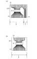
本実施形態の液晶表示装置1によれば、入力用FPC50が液晶パネル10のゲートドライバIC用配線13にゲート信号を直接入力するので、ソースCOF20にゲート信号用配線を設ける必要がない。図3(a)はゲート信号用配線が形成されたソースCOF120を模式的に示す平面図であり、図3(b)はゲート信号用配線がないソースCOF20を模式的に示す平面図である。 According to the liquid crystal display device 1 of the present embodiment, since the
図3(a)に示すように、ソースCOF120はゲート信号用配線24を有するので、ソース出力領域Bだけでなく、ゲート出力領域Cも有する。したがって、フィルム基材のサイズが大きくなり、製造コストを上昇させる。また、現状の製造設備では、複数のソースCOFをアライメントする際に、同じ大きさのソースCOFを用いる必要があるので、ゲート信号用配線24が無駄になるソースCOF120を用いることになり、製造コストがさらに上昇する。 As shown in FIG. 3A, since the
本実施形態では、ゲート出力領域がなく、ソース出力領域Bのみを有するソースCOF20を用いることができるので、フィルム基材のサイズが図3(a)に示すソースCOF120よりも小さくなり、製造コストを削減することができる。 In the present embodiment, since the
次に、本実施形態の液晶表示装置1を製造する工程について説明する。但し、液晶パネル10、ソースCOF20、ゲートCOF30、ソースPCB40、入力用FPC50の各構成要素については、公知の方法により製造することができるので説明を省略する。
まず、液晶パネル10の周縁部に異方性導電膜61を貼り付ける。液晶パネル10のアライメントマークとソースCOF20のアライメントマークとの位置合せを行って、ソースCOF20を液晶パネル10の周縁部にて仮留めする。液晶パネル10のアライメントマークと入力用FPC50のアライメントマークとの位置合せを行って、入力用FPC50を液晶パネル10の周縁部にて仮留めする。約200 ℃に加熱し、2MPaの圧力により、ソースCOF20および入力用FPC50を液晶パネル10に本接続する。Next, a process for manufacturing the liquid crystal display device 1 of the present embodiment will be described. However, each component of the
First, an anisotropic
次に、液晶パネル10の周縁部に異方性導電膜62を貼り付ける。液晶パネル10のアライメントマークとゲートCOF30のアライメントマークとの位置合せを行って、ゲートCOF30を液晶パネル10の周縁部にて仮留めする。約200 ℃に加熱し、2MPaの圧力により、ゲートCOF30を液晶パネル10に本接続する。 Next, an anisotropic
ソースPCB40に異方性導電膜63を貼り付ける。ソースPCB40のアライメントマークとソースCOF20および入力用FPC50のアライメントマークとの位置合せを行って、約200 ℃に加熱し、2MPaの圧力により、ソースCOF20および入力用FPC50をソースPCB40に本接続する。入力用FPC50の他方端部をコントロール基板(不図示)にコネクタ接続する。 An anisotropic
なお、本実施形態では、ソースCOF20を液晶パネル10に本接続した後に、ゲートCOF30を液晶パネル10に本接続しているが、ソースCOF20を液晶パネル10に本接続した後に、ソースCOF20をソースPCB40に本接続しても良い。さらに、ゲートCOF30を液晶パネル10に本接続した後に、ソースCOF20を液晶パネル10に本接続しても良い。 In this embodiment, the
本実施形態によれば、入力用FPC50を異方性導電膜63によりソースPCB40に接続することができるので、ソースPCB40にコネクタを設ける必要がなく、コストダウンが可能となる。また、半田を使わずに接続することができるので、鉛フリーの基板となり、環境にもやさしい
本実施形態によれば、ソースCOF20の接続と同時に入力用FPC50を接続することができるので、入力用FPC50を接続するための別の工程を追加する必要がなく、製造効率が良い。また、ソースCOF20と液晶パネル10(およびソースPCB40)との接続部が、入力用FPC50と液晶パネル10(およびソースPCB40)との接続部と同一ライン上にあるので、既存の製造設備を大幅に変更することなく接続を行うことができる。すなわち、接続点数の削減により、作業コストを削減できるとともに、スループットも向上する。さらに部品点数が削減できるので、部品コストを削減できる。According to the present embodiment, since the
(実施形態2)
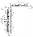
本実施形態は、本発明の第3の局面による入力用配線フィルムおよび表示装置の実施形態である。図4は実施形態2の液晶表示装置2を模式的に示す平面図である。なお、実施形態1と同一の構成要素に同一の参照符号を付すことにより、その説明を省略する。(Embodiment 2)
The present embodiment is an embodiment of an input wiring film and a display device according to the third aspect of the present invention. FIG. 4 is a plan view schematically showing the liquid
本実施形態では、ソース信号の一部が液晶パネル10上の配線14を経由して、隣接するソースCOF20を順次伝播する。言い換えれば、液晶パネル10には、ソースCOF20のソースドライバIC21へソース信号を入力するためのソース用パネル側配線14と、隣接するソースCOF20へ信号を順次伝播させるためのパネル側中継配線とが形成されている。また、ソースCOF20にも、隣接するソースCOF20へソース信号を順次伝播させるための中継配線が形成されている。さらに、ソースPCB40には、ソース用パネル側配線14に一部のソース信号を入力するための配線53が形成されている。 In the present embodiment, a part of the source signal sequentially propagates through the
実施形態1と同様にして、ソースCOF20および入力用FPC50を液晶パネル10に本接続すると、ソースCOF20の中継配線がパネル側中継配線と接続されるとともに、入力用FPC50の配線53がソース用パネル側配線14と接続される。 When the source COF 20 and the
本実施形態によれば、ソースPCB40上の配線数が減少するので、ソースPCB40のサイズが縮小して、基板コストを削減することができる。また、ソースPCB40とソースCOF20との接続部分の端子数が削減されるので、端子のピッチを広く取ることができ、接続が容易になる。したがって、良品率が向上し、ソースPCB40の長尺化に対応可能となる。 According to this embodiment, since the number of wirings on the
(実施形態3)
本実施形態は、本発明の第4の局面による入力用配線フィルムおよび表示装置の実施形態である。図5は実施形態3の液晶表示装置3を模式的に示す平面図である。なお、実施形態1と同一の構成要素に同一の参照符号を付すことにより、その説明を省略する。(Embodiment 3)
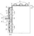
The present embodiment is an embodiment of an input wiring film and a display device according to the fourth aspect of the present invention. FIG. 5 is a plan view schematically showing the liquid
液晶パネル10のサイズが大型化するに伴って、ソースPCBも長くする必要があるが、PCBの製造装置の制約や仕上がり精度などの観点から、ソースPCBの長尺化にも限界がある。例えば、26インチ以上のサイズの液晶パネル10では、ソースPCBを2枚並べている。そして、各ソースPCBのそれぞれに入力用FPCを接続している。 As the size of the
本実施形態の液晶表示装置3は、2枚のソースPCB40a,40bを備えている。各ソースPCB40a,40bには、ソースドライバ用配線41a,41bが形成され、ソースCOF20a,20bが接続されている。本実施形態の液晶表示装置3は、中継FPC70をさらに備える。中継FPC70は、フィルム基材と、フィルム基材に形成された入力用配線(中継配線)71とを有する。中継FPC70のフィルム基材は、2枚のソースPCB40a,40bにそれぞれ接続される領域と、液晶パネル10に接続される領域とを有する。中継配線71は、第1のソースPCB40aのソースドライバ用配線41aと、第2のソースPCB40bのソースドライバ用配線41bとを中継する。 The liquid
中継FPC70は、入力用FPC50と同様に、ソースCOF20のアライメントと別工程によりアライメントする必要があるが、ソースCOF20の本接続と同時に接続することができる。すなわち、効率良く製造することができる。 Similar to the
本実施形態によれば、中継FPC70を2枚のソースPCB40a,40bに接続することにより、中継配線71を介して、第1のソースPCB40aのソースドライバ用配線41aと、第2のソースPCB40bのソースドライバ用配線41bとを接続することができる。すなわち、1枚の入力用FPC50からの入力のみで、パネル全体を駆動することができる。 According to the present embodiment, by connecting the
(実施形態4)
本実施形態は、本発明の第1の局面による入力用配線フィルムおよび表示装置の実施形態である。図6は実施形態4の液晶表示装置4を模式的に示す平面図である。なお、実施形態1および3と同一の構成要素に同一の参照符号を付すことにより、その説明を省略する。(Embodiment 4)
The present embodiment is an embodiment of an input wiring film and a display device according to the first aspect of the present invention. FIG. 6 is a plan view schematically showing the liquid
本実施形態の液晶表示装置4は、実施形態3に示す中継FPC70ではソース信号の伝送ができないときの対応例である。本実施形態では図3(a)に示すソースCOF120を介してゲート信号をゲートドライバICに供給する。より具体的に述べれば、ゲート信号は、第1の入力用FPC50aに形成されたゲート入力用配線52、第1のソースPCB40に形成されたゲート用配線43、第1のソースCOF120aに形成されたゲート信号用配線を順次通過して、ゲートドライバIC用配線13に入力され、さらに各ゲートCOF30のゲートドライバICに入力される。 The liquid
また、ソース信号は、各入力用FPC50a,50bにそれぞれ形成されたソース入力用配線51a,51b、各ソースPCB40a,40bにそれぞれ形成されたソースドライバ用配線41a,41bを順次通過して、各ソースCOF120a,120bのソースドライバICに入力される。 The source signal sequentially passes through the
本実施形態の入力用FPC50a,50bは、異方性導電膜63を介して、ソースPCB40a,40bに接続されているので、ソースPCB40a,40bにコネクタを設ける必要がなく、コストダウンが可能となる。また、ソースCOF120a,120bの接続と同時に入力用FPC50a,50bを接続することができるので、入力用FPC50a,50bを接続するための別の工程を追加する必要がなく、製造効率が良い。さらに、ソースCOF120a,120bと液晶パネル10(およびソースPCB40a,40b)との接続部が、入力用FPC50と液晶パネル10(およびソースPCB40a,40b)との接続部と同一ライン上にあるので、既存の製造設備を大幅に変更することなく接続を行うことができる。 Since the
仮に、入力用FPC50a,50bに液晶パネル10に接続される部分がなく、ソースPCB40a,40bとのみ接続される場合を想定する。この場合、ソースCOF120a,120bを液晶パネル10に本接続し、ソースPCB40a,40bに仮留めを行った後に、入力用FPC50a,50bをソースPCB40a,40bに位置合わせすることになり、本実施形態の場合よりも、アライメントが困難になる。 It is assumed that the
なお、入力用FPC50a,50bは、他の配線をさらに有していても良い。例えば、カラーフィルタ基板12の共通電極にコモン信号を入力するための配線や各ソースCOF120a,120bへソース信号の一部を順次伝播させるための配線をさらに有していても良い。これらの配線は、異方性導電膜61を介して液晶パネル10に接続されても良い。 Note that the
(実施形態5)
本実施形態は、本発明の第5の局面による入力用配線フィルムおよび表示装置の実施形態である。図7は実施形態5の液晶表示装置5を模式的に示す平面図である。なお、実施形態1および4と同一の構成要素に同一の参照符号を付すことにより、その説明を省略する。(Embodiment 5)
The present embodiment is an embodiment of an input wiring film and a display device according to the fifth aspect of the present invention. FIG. 7 is a plan view schematically showing the liquid
本実施形態の液晶表示装置5は、いわば実施形態2と実施形態3とを組み合わせたものである。具体的には、本実施形態の入力用FPC50cは、実施形態2の中継FPC70と実施形態3の入力用FPC50aとを組み合わせたものであり、第1のソースPCB40aのゲート用配線43にゲート信号を入力する機能と、各ソースPCB40a,40bの各ソースドライバ用配線41a,41bを接続する機能とを併せ持つ。 The liquid
本実施形態によれば、実施形態4との比較において、入力用FPCの数を削減することができ、入力箇所が1箇所になるという利点がある。具体的には、実施形態4の場合、ソースPCB40a,40bに対してそれぞれ入力用FPC50a,50bが接続され、さらに各入力用FPC50a,50bがコントロール基板(不図示)にそれぞれコネクタ接続されている。これに対して、本実施形態では、ただ1つの入力用FPC50cがコントロール基板80のコネクタ81に接続されている。したがって、材料費を削減することができ、工数も低減することができる。 According to the present embodiment, in comparison with the fourth embodiment, there is an advantage that the number of input FPCs can be reduced and the number of input locations is one. Specifically, in the case of the fourth embodiment, the
以上、本発明の好ましい実施形態について説明したが、本発明の技術的範囲は上記実施形態に記載の範囲に限定されない。上記実施形態が例示であり、それらの各構成要素や各処理プロセスの組合せに、さらにいろいろな変形例が可能なこと、またそうした変形例も本発明の範囲にあることは当業者に理解されるところである。例えば、上記実施形態ではソースPCBを用いているが、FPCなどのフレキシブルな基板を用いても良い。フレキシブルな基板を使用することにより、ソースCOFとの接続時に発生する熱応力が緩和され、ソースCOFに形成された配線の断線不良が発生し難くなる。 As mentioned above, although preferable embodiment of this invention was described, the technical scope of this invention is not limited to the range as described in the said embodiment. It is understood by those skilled in the art that the above embodiment is an exemplification, and that various modifications can be made to the combination of each component and each processing process, and such modifications are also within the scope of the present invention. By the way. For example, although the source PCB is used in the above embodiment, a flexible substrate such as an FPC may be used. By using a flexible substrate, the thermal stress generated at the time of connection with the source COF is relieved, and the disconnection failure of the wiring formed in the source COF becomes difficult to occur.
また、ソースPCB上に液晶制御回路や外部インターフェース回路あるいは電源電圧を安定化させるためのチップ部品などの部品を一切搭載しない構成も可能である。これにより、基板の加工費がゼロになる。なお、この場合には、ソースCOFにチップ部品を搭載することもできる。 Further, a configuration in which no components such as a liquid crystal control circuit, an external interface circuit, or a chip component for stabilizing the power supply voltage are mounted on the source PCB is also possible. Thereby, the processing cost of a board | substrate becomes zero. In this case, a chip component can be mounted on the source COF.
本発明の入力用配線フィルムは、液晶モジュールなどのFPD(フラットパネルディスプレイ)モジュールにおける周辺回路の実装に利用することができる。また本発明の表示装置は各種の電気機器に利用することができる。例えば、携帯電話機、PDA(Personal Digital Assistance )、パーソナルコンピュータ、薄型テレビ、医療用ディスプレイ、カーナビゲーションシステム、アミューズメント機器などに利用することができる。 The input wiring film of the present invention can be used for mounting peripheral circuits in FPD (flat panel display) modules such as liquid crystal modules. In addition, the display device of the present invention can be used for various electric devices. For example, it can be used for mobile phones, PDAs (Personal Digital Assistance), personal computers, flat-screen TVs, medical displays, car navigation systems, amusement devices, and the like.
1,2,3,4,5 液晶表示装置
10 液晶パネル
11 TFT基板
12 カラーフィルタ基板
13 ゲートドライバIC用配線
14 ソース用パネル側配線
20,20a,20b ソースCOF
21 ソースドライバIC
22 入力配線
23 出力配線
24 ゲート信号用配線
30 ゲートCOF
40,40a,40b ソースPCB
41,41a,41b ソースドライバ用配線
43 ゲート用配線
50,50a,50b,50c 入力用FPC
51,51a,51b ソース入力用配線
52 ゲート入力用配線
61,62,63 異方性導電膜
70 中継FPC
71 中継配線
80 コントロール基板
81 コネクタ
120,120a,120b ソースCOF1, 2, 3, 4, 5 Liquid
21 Source Driver IC
22
40, 40a, 40b Source PCB
41, 41a, 41b
51, 51a, 51b
71
Claims (12)
Translated fromJapanese前記表示装置は、第1信号配線を有する表示パネルと、前記第1信号配線に接続され、前記第1信号配線への信号の出力を制御する第1回路を有する第1回路フィルムと、前記第1回路フィルムに接続され、前記第1回路に信号を入力するための第1回路用配線を有する配線基板とを備え、
前記フィルム基材は、前記配線基板に接続される領域と、前記表示パネルに接続される領域とを有し、前記入力用配線は前記第1回路用配線に信号を入力するための第1入力用配線を少なくとも含み、前記フィルム基材と前記配線基板とが接続されることによって、前記第1入力用配線が前記第1回路用配線と接続される入力用配線フィルム。An input wiring film having a film base material and an input wiring formed on the film base material for inputting a signal to a display device,
The display device includes a display panel having a first signal wiring, a first circuit film connected to the first signal wiring and having a first circuit that controls output of a signal to the first signal wiring, A circuit board connected to one circuit film and having a first circuit wiring for inputting a signal to the first circuit;
The film base has a region connected to the wiring substrate and a region connected to the display panel, and the input wiring is a first input for inputting a signal to the first circuit wiring. An input wiring film including at least a wiring for wiring, wherein the first input wiring is connected to the first circuit wiring by connecting the film base and the wiring substrate.
前記表示装置は、第1信号配線および第2信号配線を有する表示パネルと、前記第1信号配線に接続され、前記第1信号配線への信号の出力を制御する第1回路を有する第1回路フィルムと、前記第1回路フィルムに接続され、前記第1回路へ信号を入力するための第1回路用配線を有する配線基板と、前記第2信号配線に接続され、前記第2信号配線への信号の出力を制御する第2回路を有する第2回路フィルムとを備え、前記表示パネルが前記第2回路へ信号を入力するための第2回路用配線を有しており、
前記フィルム基材は、前記配線基板に接続される領域と、前記表示パネルに接続される領域とを有し、前記入力用配線は、前記第1回路用配線に信号を入力するための第1入力用配線と、前記第2回路用配線に信号を入力するための第2入力用配線とを含み、前記フィルム基材と前記配線基板とが接続されることによって、前記第1入力用配線が前記第1回路用配線と接続され、前記フィルム基材と前記表示パネルとが接続されることによって、前記第2入力用配線が前記第2回路用配線と接続される入力用配線フィルム。An input wiring film having a film base material and an input wiring formed on the film base material for inputting a signal to a display device,
The display device includes a display panel having a first signal wiring and a second signal wiring, and a first circuit having a first circuit connected to the first signal wiring and controlling output of a signal to the first signal wiring. A film, a wiring board connected to the first circuit film and having a first circuit wiring for inputting a signal to the first circuit, and connected to the second signal wiring, to the second signal wiring; A second circuit film having a second circuit for controlling the output of a signal, the display panel having a second circuit wiring for inputting a signal to the second circuit,
The film base has a region connected to the wiring substrate and a region connected to the display panel, and the input wiring is a first for inputting a signal to the first circuit wiring. An input wiring and a second input wiring for inputting a signal to the second circuit wiring, and the first base wiring and the wiring substrate are connected to each other so that the first input wiring is An input wiring film that is connected to the first circuit wiring and that connects the second input wiring to the second circuit wiring by connecting the film substrate and the display panel.
前記表示装置は、第1信号配線および第2信号配線を有する表示パネルと、前記第1信号配線に接続され、前記第1信号配線への信号の出力を制御する第1回路を有する第1回路フィルムと、前記第1回路フィルムに接続され、前記第1回路へ信号を入力するための第1回路用配線を有する配線基板と、前記第2信号配線に接続され、前記第2信号配線への信号の出力を制御する第2回路を有する第2回路フィルムとを備え、前記表示パネルが前記第1回路へ信号を入力するための第1回路用パネル側配線と、前記第2回路へ信号を入力するための第2回路用配線とを有しており、
前記フィルム基材は、前記配線基板に接続される領域と、前記表示パネルに接続される領域とを有し、前記入力用配線は、前記第1回路用配線に信号を入力するための第1入力用配線と、前記第2回路用配線に信号を入力するための第2入力用配線と、前記第1回路用パネル側配線に信号を入力するための第3入力用配線とを含み、前記フィルム基材と前記配線基板とが接続されることによって、前記第1入力用配線が前記第1回路用配線と接続され、前記フィルム基材と前記表示パネルとが接続されることによって、前記第2入力用配線が前記第2回路用配線と接続されるとともに、前記第3入力用配線が前記第1回路用パネル側配線と接続される入力用配線フィルム。An input wiring film having a film base material and an input wiring formed on the film base material for inputting a signal to a display device,
The display device includes a display panel having a first signal wiring and a second signal wiring, and a first circuit having a first circuit connected to the first signal wiring and controlling output of a signal to the first signal wiring. A film, a wiring board connected to the first circuit film and having a first circuit wiring for inputting a signal to the first circuit, and connected to the second signal wiring, to the second signal wiring; A second circuit film having a second circuit for controlling the output of the signal, the panel-side wiring for the first circuit for the display panel to input the signal to the first circuit, and the signal to the second circuit A second circuit wiring for input,
The film base has a region connected to the wiring substrate and a region connected to the display panel, and the input wiring is a first for inputting a signal to the first circuit wiring. An input wiring; a second input wiring for inputting a signal to the second circuit wiring; and a third input wiring for inputting a signal to the first circuit panel wiring; By connecting the film base and the wiring substrate, the first input wiring is connected to the first circuit wiring, and the film base and the display panel are connected to each other. An input wiring film in which two input wirings are connected to the second circuit wiring and the third input wiring is connected to the first circuit panel side wiring.
前記表示装置は、複数の第1信号配線を有する表示パネルと、前記複数の第1信号配線のうちの少なくとも1つの第1信号配線に接続され、前記少なくとも1つの第1信号配線への信号の出力を制御する第1回路をそれぞれ有する複数の第1回路フィルムと、前記複数の第1回路フィルムのうちの少なくとも1つの第1回路フィルムにそれぞれ接続され、前記少なくとも1つの第1回路へ信号を入力するための第1回路用配線をそれぞれ有する第1および第2配線基板とを備え、
前記フィルム基材は、前記第1および第2配線基板にそれぞれ接続される領域と、前記表示パネルに接続される領域とを有し、前記入力用配線は、前記第1配線基板の第1回路用配線と、前記第2配線基板の第1回路用配線とを中継する中継配線を含み、前記フィルム基材と前記第1および第2配線基板とが接続されることによって、前記第1配線基板の第1回路用配線と前記第2配線基板の第1回路用配線とが前記中継配線を介して接続される入力用配線フィルム。An input wiring film having a film base material and an input wiring formed on the film base material for inputting a signal to a display device,
The display device is connected to a display panel having a plurality of first signal wirings and at least one first signal wiring of the plurality of first signal wirings, and a signal to the at least one first signal wiring is transmitted. A plurality of first circuit films each having a first circuit for controlling an output, and each of the plurality of first circuit films is connected to at least one first circuit film, and a signal is transmitted to the at least one first circuit. First and second wiring boards each having a first circuit wiring for input,
The film base has a region connected to each of the first and second wiring substrates and a region connected to the display panel, and the input wiring is a first circuit of the first wiring substrate. A relay wiring that relays the wiring for wiring and the first circuit wiring of the second wiring board, and the film base and the first and second wiring boards are connected, whereby the first wiring board An input wiring film in which the first circuit wiring and the first circuit wiring of the second wiring board are connected via the relay wiring.
前記表示装置は、複数の第1信号配線と第2信号配線とを有する表示パネルと、前記複数の第1信号配線のうちの少なくとも1つの第1信号配線に接続され、前記少なくとも1つの第1信号配線への信号の出力を制御する第1回路をそれぞれ有する複数の第1回路フィルムと、前記複数の第1回路フィルムのうちの少なくとも1つの第1回路フィルムにそれぞれ接続され、前記少なくとも1つの第1回路へ信号を入力するための第1回路用配線をそれぞれ有する第1および第2配線基板と、前記第2信号配線に接続され、前記第2信号配線への信号の出力を制御する第2回路を有する第2回路フィルムとを備え、前記第1配線基板は前記第2回路へ信号を入力するための第2回路用配線を有しており、
前記フィルム基材は、前記第1および第2配線基板にそれぞれ接続される領域と、前記表示パネルに接続される領域とを有し、前記入力用配線は、前記第1配線基板の前記第1回路用配線に信号を入力するための第1配線基板用配線と、前記第2配線基板の前記第1回路用配線に信号を入力するための第2配線基板用配線と、前記第2回路用配線に信号を入力するための第2入力用配線とを含み、前記フィルム基材と前記第1および第2配線基板とが接続されることによって、前記第1配線基板用配線が前記第1配線基板の前記第1回路用配線と接続され、前記第2配線基板用配線が前記第2配線基板の前記第1回路用配線と接続されるとともに、前記第2入力用配線が前記第2回路用配線と接続される入力用配線フィルム。An input wiring film having a film base material and an input wiring formed on the film base material for inputting a signal to a display device,
The display device is connected to a display panel having a plurality of first signal lines and a second signal line, and to at least one first signal line of the plurality of first signal lines, and the at least one first signal line. A plurality of first circuit films each having a first circuit for controlling output of a signal to the signal wiring; and at least one first circuit film of the plurality of first circuit films, respectively, First and second wiring boards each having a first circuit wiring for inputting a signal to the first circuit, and a second circuit connected to the second signal wiring and controlling the output of the signal to the second signal wiring. A second circuit film having two circuits, the first wiring board has a second circuit wiring for inputting a signal to the second circuit,
The film base has a region connected to each of the first and second wiring boards and a region connected to the display panel, and the input wiring is the first wiring board of the first wiring board. A wiring for a first wiring board for inputting a signal to the wiring for a circuit, a wiring for a second wiring board for inputting a signal to the wiring for the first circuit of the second wiring board, and for the second circuit A second input wiring for inputting a signal to the wiring, and the first wiring board wiring is connected to the first wiring board by connecting the film base and the first and second wiring boards. The wiring for the first circuit is connected to the wiring for the first circuit, the wiring for the second wiring board is connected to the wiring for the first circuit of the second wiring board, and the wiring for the second input is for the second circuit. Wiring film for input connected to wiring.
フィルム基材と、前記フィルム基材に形成され、前記第1回路用配線に信号を入力するための第1入力用配線とを有する入力用配線フィルムをさらに備え、前記フィルム基材は前記配線基板に接続されるとともに、前記表示パネルに接続され、前記フィルム基材と前記配線基板とが接続されることによって、前記第1入力用配線が前記第1回路用配線と接続されている表示装置。A display panel having a first signal wiring, a first circuit film having a first circuit connected to the first signal wiring and controlling a signal output to the first signal wiring, and connected to the first circuit film A display device comprising at least a wiring substrate having a first circuit wiring for inputting a signal to the first circuit,
The film substrate further includes an input wiring film formed on the film substrate and having a first input wiring for inputting a signal to the first circuit wiring, and the film base is the wiring substrate A display device in which the first input wiring is connected to the first circuit wiring by being connected to the display panel and connected to the film base and the wiring board.
フィルム基材と、前記フィルム基材に形成された入力用配線とを有する入力用配線フィルムをさらに備え、前記入力用配線は、前記第1回路用配線に信号を入力するための第1入力用配線と、前記第2回路用配線に信号を入力するための第2入力用配線とを含み、前記フィルム基材は前記配線基板に接続されるとともに、前記表示パネルに接続され、前記フィルム基材と前記配線基板とが接続されることによって、前記第1入力用配線が前記第1回路用配線と接続され、前記フィルム基材と前記表示パネルとが接続されることによって、前記第2入力用配線が前記第2回路用配線と接続されている表示装置。A display panel having a first signal line and a second signal line; a first circuit film having a first circuit connected to the first signal line and controlling output of a signal to the first signal line; A wiring board connected to one circuit film and having a first circuit wiring for inputting a signal to the first circuit, and a signal output to the second signal wiring connected to the second signal wiring A display device having at least a second circuit film having a second circuit, wherein the display panel has a second circuit wiring for inputting a signal to the second circuit,
An input wiring film having a film base and an input wiring formed on the film base is further provided, and the input wiring is a first input for inputting a signal to the first circuit wiring. Wiring and a second input wiring for inputting a signal to the second circuit wiring, and the film base is connected to the wiring substrate and connected to the display panel, and the film base And the wiring board are connected, the first input wiring is connected to the first circuit wiring, and the film base and the display panel are connected to each other for the second input. A display device in which wiring is connected to the second circuit wiring.
フィルム基材と、前記フィルム基材に形成された入力用配線とを有する入力用配線フィルムをさらに備え、前記入力用配線は、前記第1回路用配線に信号を入力するための第1入力用配線と、前記第2回路用配線に信号を入力するための第2入力用配線と、前記第1回路用パネル側配線に信号を入力するための第3入力用配線とを含み、前記フィルム基材は前記配線基板に接続されるとともに、前記表示パネルに接続され、前記フィルム基材と前記配線基板とが接続されることによって、前記第1入力用配線が前記第1回路用配線と接続され、前記フィルム基材と前記表示パネルとが接続されることによって、前記第2入力用配線が前記第2回路用配線と接続されるとともに、前記第3入力用配線が前記第1回路用パネル側配線と接続されている表示装置。A display panel having a first signal line and a second signal line; a first circuit film having a first circuit connected to the first signal line and controlling output of a signal to the first signal line; A wiring board connected to one circuit film and having a first circuit wiring for inputting a signal to the first circuit, and a signal output to the second signal wiring connected to the second signal wiring At least a second circuit film having a second circuit, and a display panel side wiring for the display panel to input a signal to the first circuit, and a signal to be input to the second circuit. A display device having a second circuit wiring,
An input wiring film having a film base and an input wiring formed on the film base is further provided, and the input wiring is a first input for inputting a signal to the first circuit wiring. Including a wiring, a second input wiring for inputting a signal to the second circuit wiring, and a third input wiring for inputting a signal to the first circuit panel wiring. The material is connected to the wiring board, is connected to the display panel, and the film base and the wiring board are connected, whereby the first input wiring is connected to the first circuit wiring. By connecting the film substrate and the display panel, the second input wiring is connected to the second circuit wiring, and the third input wiring is connected to the first circuit panel side. Connected with wiring That display device.
フィルム基材と、前記フィルム基材に形成された入力用配線とを有する入力用配線フィルムをさらに備え、前記入力用配線は、前記第1配線基板の第1回路用配線と、前記第2配線基板の第1回路用配線とを中継する中継配線を含み、前記フィルム基材は、前記第1および第2配線基板にそれぞれ接続されるとともに、前記表示パネルに接続され、前記フィルム基材と前記第1および第2配線基板とが接続されることによって、前記第1配線基板の第1回路用配線と前記第2配線基板の第1回路用配線とが前記中継配線を介して接続されている表示装置。A display panel having a plurality of first signal lines and a first panel connected to at least one first signal line of the plurality of first signal lines and controlling output of signals to the at least one first signal line. A plurality of first circuit films each having one circuit and a first circuit film connected to at least one first circuit film of the plurality of first circuit films and for inputting a signal to the at least one first circuit; A display device comprising at least first and second wiring boards each having one circuit wiring,
An input wiring film further comprising a film base and an input wiring formed on the film base, wherein the input wiring includes the first circuit wiring of the first wiring board and the second wiring. Including a relay wiring that relays the first circuit wiring of the substrate, and the film base is connected to the first and second wiring boards, and is connected to the display panel, and the film base and the By connecting the first and second wiring boards, the first circuit wiring of the first wiring board and the first circuit wiring of the second wiring board are connected via the relay wiring. Display device.
フィルム基材と、前記フィルム基材に形成された入力用配線とを有する入力用配線フィルムをさらに備え、前記入力用配線は、前記第1配線基板の前記第1回路用配線に信号を入力するための第1配線基板用配線と、前記第2配線基板の前記第1回路用配線に信号を入力するための第2配線基板用配線と、前記第2回路用配線に信号を入力するための第2入力用配線とを含み、前記フィルム基材は、前記第1および第2配線基板にそれぞれ接続されるとともに、前記表示パネルに接続され、前記フィルム基材と前記第1および第2配線基板とが接続されることによって、前記第1配線基板用配線が前記第1配線基板の前記第1回路用配線と接続され、前記第2配線基板用配線が前記第2配線基板の前記第1回路用配線と接続されるとともに、前記第2入力用配線が前記第2回路用配線と接続されている表示装置。A display panel having a plurality of first signal lines and a second signal line, and a signal connected to at least one first signal line of the plurality of first signal lines and to the at least one first signal line A plurality of first circuit films each having a first circuit for controlling the output of the first circuit film, and at least one first circuit film of the plurality of first circuit films, respectively, and a signal to the at least one first circuit First and second wiring boards each having a first circuit wiring for inputting a signal, and a second circuit connected to the second signal wiring and controlling the output of a signal to the second signal wiring. A display device having a second circuit wiring for inputting a signal to the second circuit;
An input wiring film having a film base and an input wiring formed on the film base is further provided, and the input wiring inputs a signal to the first circuit wiring of the first wiring board. A wiring for a first wiring board, a wiring for a second wiring board for inputting a signal to the wiring for the first circuit of the second wiring board, and a signal for inputting a signal to the wiring for the second circuit The film base is connected to the first and second wiring boards and connected to the display panel, and the film base and the first and second wiring boards. Are connected, the first wiring board wiring is connected to the first circuit wiring of the first wiring board, and the second wiring board wiring is connected to the first circuit of the second wiring board. Connected with wiring for Display device whose serial second input line is connected to the second circuit wiring.
Priority Applications (1)
| Application Number | Priority Date | Filing Date | Title |
|---|---|---|---|
| JP2004227149AJP4304134B2 (en) | 2004-08-03 | 2004-08-03 | WIRING FILM FOR INPUT AND DISPLAY DEVICE HAVING THE SAME |
Applications Claiming Priority (1)
| Application Number | Priority Date | Filing Date | Title |
|---|---|---|---|
| JP2004227149AJP4304134B2 (en) | 2004-08-03 | 2004-08-03 | WIRING FILM FOR INPUT AND DISPLAY DEVICE HAVING THE SAME |
Publications (2)
| Publication Number | Publication Date |
|---|---|
| JP2006049514A JP2006049514A (en) | 2006-02-16 |
| JP4304134B2true JP4304134B2 (en) | 2009-07-29 |
Family
ID=36027741
Family Applications (1)
| Application Number | Title | Priority Date | Filing Date |
|---|---|---|---|
| JP2004227149AExpired - Fee RelatedJP4304134B2 (en) | 2004-08-03 | 2004-08-03 | WIRING FILM FOR INPUT AND DISPLAY DEVICE HAVING THE SAME |
Country Status (1)
| Country | Link |
|---|---|
| JP (1) | JP4304134B2 (en) |
Cited By (3)
| Publication number | Priority date | Publication date | Assignee | Title |
|---|---|---|---|---|
| CN107564421A (en)* | 2016-06-30 | 2018-01-09 | 乐金显示有限公司 | Flexible organic light-emitting display device |
| WO2018019022A1 (en)* | 2016-07-29 | 2018-02-01 | Boe Technology Group Co., Ltd. | Array substrate, fabricating method thereof, and display device |
| US10312313B2 (en) | 2016-09-07 | 2019-06-04 | Samsung Display Co., Ltd. | Display device |
Families Citing this family (16)
| Publication number | Priority date | Publication date | Assignee | Title |
|---|---|---|---|---|
| KR101352344B1 (en)* | 2006-09-13 | 2014-01-15 | 삼성디스플레이 주식회사 | Signal transfer member and display apparatus having the same |
| US8289258B2 (en) | 2007-03-16 | 2012-10-16 | Lg Display Co., Ltd. | Liquid crystal display |
| US20100182293A1 (en)* | 2007-07-04 | 2010-07-22 | Kohji Minamino | Display module, liquid crystal display device and method for manufacturing display module |
| JP5339274B2 (en)* | 2008-09-03 | 2013-11-13 | 株式会社ジャパンディスプレイ | Display device |
| JP5899535B2 (en)* | 2012-02-01 | 2016-04-06 | 株式会社Joled | EL display device |
| US9595222B2 (en) | 2012-10-09 | 2017-03-14 | Joled Inc. | Image display apparatus |
| WO2014061231A1 (en) | 2012-10-17 | 2014-04-24 | パナソニック株式会社 | Gate driver integrated circuit, and image display device using same |
| US9773450B2 (en) | 2012-10-17 | 2017-09-26 | Joled Inc. | EL display panel with gate driver circuits mounted on flexible board including terminal connection lines connecting connection parts and control terminals |
| JP6161929B2 (en)* | 2013-03-22 | 2017-07-12 | 株式会社三共 | Game machine |
| CN103700657B (en)* | 2013-12-12 | 2016-08-17 | 京东方科技集团股份有限公司 | Array base palte and preparation method thereof, display device |
| CN104134420B (en)* | 2014-08-14 | 2017-01-18 | 广东威创视讯科技股份有限公司 | Displayer based on FPC bonding |
| JP6560887B2 (en)* | 2015-04-08 | 2019-08-14 | 株式会社ジャパンディスプレイ | Transistor substrate and display device |
| JP6789230B2 (en)* | 2016-07-11 | 2020-11-25 | 京東方科技集團股▲ふん▼有限公司Boe Technology Group Co.,Ltd. | Chip-on-film, flexible display device equipped with it, and manufacturing method thereof |
| KR101853032B1 (en)* | 2016-07-21 | 2018-06-05 | 엘지디스플레이 주식회사 | Display Device |
| KR102629350B1 (en)* | 2018-12-12 | 2024-01-25 | 삼성디스플레이 주식회사 | Display device and manufacturing method thereof |
| CN115003006B (en)* | 2021-11-03 | 2023-04-14 | 荣耀终端有限公司 | A circuit board, electronic equipment and testing method |
- 2004
- 2004-08-03JPJP2004227149Apatent/JP4304134B2/ennot_activeExpired - Fee Related
Cited By (6)
| Publication number | Priority date | Publication date | Assignee | Title |
|---|---|---|---|---|
| CN107564421A (en)* | 2016-06-30 | 2018-01-09 | 乐金显示有限公司 | Flexible organic light-emitting display device |
| CN107564421B (en)* | 2016-06-30 | 2019-12-03 | 乐金显示有限公司 | Flexible organic light-emitting display device |
| WO2018019022A1 (en)* | 2016-07-29 | 2018-02-01 | Boe Technology Group Co., Ltd. | Array substrate, fabricating method thereof, and display device |
| US10304682B2 (en) | 2016-07-29 | 2019-05-28 | Boe Technology Group Co., Ltd. | Array substrate, fabricating method thereof, and display device |
| US10573595B2 (en) | 2016-07-29 | 2020-02-25 | Beijing Boe Optoelectronics Technology Co., Ltd. | Array substrate, fabricating method thereof, and display device |
| US10312313B2 (en) | 2016-09-07 | 2019-06-04 | Samsung Display Co., Ltd. | Display device |
Also Published As
| Publication number | Publication date |
|---|---|
| JP2006049514A (en) | 2006-02-16 |
Similar Documents
| Publication | Publication Date | Title |
|---|---|---|
| JP4304134B2 (en) | WIRING FILM FOR INPUT AND DISPLAY DEVICE HAVING THE SAME | |
| TWI476738B (en) | Flexible display panel and assembly method thereof | |
| CN109860142B (en) | Chip-on-film and display device including the chip-on-film | |
| US6836310B2 (en) | Liquid crystal display device | |
| JP4314084B2 (en) | Display device | |
| JP4059750B2 (en) | Electronic module and manufacturing method thereof | |
| JP4997593B2 (en) | Display device | |
| US7420821B2 (en) | Electronic module and driving circuit board therefor | |
| WO2022205551A1 (en) | Chip-on-film group, display panel and display module | |
| KR100802458B1 (en) | Display device | |
| KR100745255B1 (en) | Circuit film and display device including the same | |
| KR100831114B1 (en) | Liquid crystal display device | |
| CN102446926B (en) | Flexible display panel and assembling method thereof | |
| JP2018093101A (en) | Flexible print circuit board and image display unit | |
| KR102120817B1 (en) | Driving integrated circuit pad unit and flat display panel having the same | |
| CN112859461A (en) | Display module assembly and display device with same | |
| JP2007298728A (en) | Display apparatus | |
| KR20180027685A (en) | Chip-On-Film Typed Driving Circuit, Circuit Film and Display Device having the same | |
| KR20140133292A (en) | Flexible printed circuit board and display device having thereof | |
| JP2007316509A (en) | Indicating element | |
| JP2004069779A (en) | Liquid crystal display | |
| JP2007322444A (en) | Display module | |
| JP2006285264A (en) | Method for packaging flexible substrate, and display apparatus | |
| KR20070040981A (en) | Flexible circuit boards and liquid crystal displays | |
| JP2007094272A (en) | Lcd module |
Legal Events
| Date | Code | Title | Description |
|---|---|---|---|
| A621 | Written request for application examination | Free format text:JAPANESE INTERMEDIATE CODE: A621 Effective date:20060912 | |
| A977 | Report on retrieval | Free format text:JAPANESE INTERMEDIATE CODE: A971007 Effective date:20090319 | |
| TRDD | Decision of grant or rejection written | ||
| A01 | Written decision to grant a patent or to grant a registration (utility model) | Free format text:JAPANESE INTERMEDIATE CODE: A01 Effective date:20090331 | |
| A01 | Written decision to grant a patent or to grant a registration (utility model) | Free format text:JAPANESE INTERMEDIATE CODE: A01 | |
| A61 | First payment of annual fees (during grant procedure) | Free format text:JAPANESE INTERMEDIATE CODE: A61 Effective date:20090427 | |
| FPAY | Renewal fee payment (event date is renewal date of database) | Free format text:PAYMENT UNTIL: 20120501 Year of fee payment:3 | |
| R150 | Certificate of patent or registration of utility model | Free format text:JAPANESE INTERMEDIATE CODE: R150 | |
| FPAY | Renewal fee payment (event date is renewal date of database) | Free format text:PAYMENT UNTIL: 20120501 Year of fee payment:3 | |
| FPAY | Renewal fee payment (event date is renewal date of database) | Free format text:PAYMENT UNTIL: 20130501 Year of fee payment:4 | |
| LAPS | Cancellation because of no payment of annual fees |