JP4300770B2 - Manufacturing method of electronic parts - Google Patents
Manufacturing method of electronic partsDownload PDFInfo
- Publication number
- JP4300770B2 JP4300770B2JP2002234782AJP2002234782AJP4300770B2JP 4300770 B2JP4300770 B2JP 4300770B2JP 2002234782 AJP2002234782 AJP 2002234782AJP 2002234782 AJP2002234782 AJP 2002234782AJP 4300770 B2JP4300770 B2JP 4300770B2
- Authority
- JP
- Japan
- Prior art keywords
- heat treatment
- oxygen concentration
- ceramic element
- internal electrode
- primary
- Prior art date
- Legal status (The legal status is an assumption and is not a legal conclusion. Google has not performed a legal analysis and makes no representation as to the accuracy of the status listed.)
- Expired - Fee Related
Links
- 238000004519manufacturing processMethods0.000titleclaimsdescription16
- 238000010438heat treatmentMethods0.000claimsdescription180
- 239000000919ceramicSubstances0.000claimsdescription59
- QVGXLLKOCUKJST-UHFFFAOYSA-Natomic oxygenChemical compound[O]QVGXLLKOCUKJST-UHFFFAOYSA-N0.000claimsdescription43
- 229910052760oxygenInorganic materials0.000claimsdescription43
- 239000001301oxygenSubstances0.000claimsdescription43
- 239000000463materialSubstances0.000claimsdescription7
- 239000002075main ingredientSubstances0.000claimsdescription2
- 239000003985ceramic capacitorSubstances0.000description14
- 239000002184metalSubstances0.000description14
- 229910052751metalInorganic materials0.000description14
- 229910052802copperInorganic materials0.000description8
- 238000005304joiningMethods0.000description6
- 238000007789sealingMethods0.000description6
- 239000011521glassSubstances0.000description4
- 238000000034methodMethods0.000description4
- 238000001556precipitationMethods0.000description4
- 230000000694effectsEffects0.000description3
- 230000000052comparative effectEffects0.000description2
- 230000007547defectEffects0.000description2
- 238000009792diffusion processMethods0.000description2
- 229910052759nickelInorganic materials0.000description2
- 230000015572biosynthetic processEffects0.000description1
- 238000007796conventional methodMethods0.000description1
- 238000005520cutting processMethods0.000description1
- 230000002950deficientEffects0.000description1
- 230000008021depositionEffects0.000description1
- 230000006866deteriorationEffects0.000description1
- 238000007598dipping methodMethods0.000description1
- 239000007772electrode materialSubstances0.000description1
- 238000010304firingMethods0.000description1
- 238000010030laminatingMethods0.000description1
- 238000012986modificationMethods0.000description1
- 230000004048modificationEffects0.000description1
- 238000005498polishingMethods0.000description1
- 239000000843powderSubstances0.000description1
Images


Landscapes
- Ceramic Capacitors (AREA)
- Fixed Capacitors And Capacitor Manufacturing Machines (AREA)
Description
Translated fromJapanese【0001】
【発明の属する技術分野】
本発明は電子部品の製造方法に関し、詳しくは、セラミック素子中に配設された内部電極が、セラミック素子の端面に引き出され、該端面に配設された外部電極に接続された構造を有する電子部品の製造方法に関する。
【0002】
【従来の技術及び発明が解決しようとする課題】
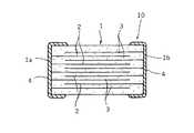
図1に示すように、代表的な電子部品の一つである表面実装型の積層セラミックコンデンサ10は、セラミック素子(電子部品素子)1中に、複数の内部電極2がセラミック層3を介して積層、配設され、かつ、セラミック層3を介して互いに対向する内部電極2が交互にセラミック素子(電子部品素子)1の逆側の端面に引き出されて、セラミック素子1の両端面に形成された一対の外部電極4に接続された構造を有している。
【0003】
そして、このような構造を有する積層セラミックコンデンサ(電子部品)10を製造する場合において、外部電極4は、通常、セラミック素子1の両端部に導電ペーストを塗布した後、所定の条件下で導電ペーストを焼き付けることにより形成されている。
【0004】
しかし、上記従来の方法で製造された積層セラミックコンデンサ(電子部品)10においては、内部電極2と外部電極4のそれぞれを構成する金属が相互拡散することによって、内部電極2と外部電極4の接合が行われており、耐湿性試験等を行う際などに、セラミック素子1の端面の、内部電極2と外部電極4の接合部分(該接合部分とセラミック層の隙間など)から、水分がセラミック素子中に侵入し、特性の劣化を招くという問題点がある。
【0005】
なお、上記の問題点は積層セラミックコンデンサに限らず、積層インダクタ、積層バリスタなど、セラミック素子中に配設された内部電極が、セラミック素子の端面に引き出され、該端面に配設された外部電極に接続された構造を有する電子部品に当てはまるものである。
【0006】
本発明は、上記問題点を解決するものであり、内部電極と外部電極の接合部分(該接合部分とセラミック層の隙間など)からの水分の浸入を防止することが可能で、信頼性の高い電子部品を効率よく製造することが可能な電子部品の製造方法を提供することを目的とする。
【0007】
【課題を解決するための手段】
上記目的を達成するために、本発明(請求項1)の電子部品の製造方法は、
セラミック素子中に配設された、Ni又はNiを主成分とする材料からなる内部電極がセラミック素子の端面に引き出され、該端面に配設されたCu又はCuを主成分とする材料からなる外部電極に接続された構造を有する電子部品の製造方法であって、
前記セラミック素子の内部電極が引き出された端面を含む領域に、導電ペーストを塗布し、
(a)熱処理温度を750〜950℃、
(b)熱処理雰囲気中の酸素濃度を50〜100ppm、
(c)熱処理時間を5〜60min
の条件に制御して熱処理を行うことにより、導電ペーストを焼き付ける一次熱処理工程と、
前記一次熱処理が行われた前記セラミック素子を常温に戻す工程と、
前記セラミック素子を、
(a’)熱処理温度を一次熱処理の熱処理温度よりも50〜100℃低くし、
(b’)熱処理雰囲気中の酸素濃度を一次熱処理の酸素濃度よりも20〜50 ppm低くし、
(c’)熱処理時間を一次熱処理の熱処理時間よりも10〜25min長くすること
の各条件を満たす熱処理条件下で熱処理する二次熱処理工程と
を具備することを特徴としている。
【0008】
セラミック素子の内部電極が引き出された端面を含む領域に導電ペーストを塗布し、(a)熱処理温度を750〜950℃、(b)熱処理雰囲気中の酸素濃度を50〜100ppm、(c)熱処理時間を5〜60minの条件に制御して熱処理(一次熱処理)を行い、導電ペーストを焼き付けた後、セラミック素子を常温に戻した後、セラミック素子を、上記の(a’),(b’),(c’)の条件のもとで二次熱処理を行うことにより、内部電極とCu又はCuを主成分とする材料からなる外部電極の接合部分に、内部電極を構成する金属を多く析出させることが可能になり、水分に対するシール性を向上させることができるようになる。
【0009】
一次熱処理工程において、熱処理温度を750〜950℃、熱処理雰囲気中の酸素濃度を50〜100ppm、熱処理時間を5〜60minとし、かつ、二次熱処理工程において、請求項1に規定されているように、熱処理温度を一次熱処理の熱処理温度よりも50〜100℃低くし、熱処理雰囲気中の酸素濃度を一次熱処理の酸素濃度よりも20〜50ppm低くし、熱処理時間を一次熱処理の熱処理時間よりも10〜25min長くするようにした場合、内部電極とCu又はCuを主成分とする材料からなる外部電極の接合部分に、内部電極を構成する金属(Ni)を多く析出させて、水分に対するシール性を向上させることが可能になる。
【0010】
なお、二次熱処理工程の熱処理温度を一次熱処理工程の熱処理温度に比べて50〜100℃低くしたのは、内部電極を構成する金属の析出量を制御するためである。すなわち、二次熱処理工程の熱処理温度を一次熱処理工程の熱処理温度と同等以上にすると、二次熱処理工程において内部電極を構成する金属が多く析出することになり、これによって内部電極が電子部品素子端面から突出し、この内部電極の突出によって、外部電極と電子部品素子との間に空洞ができる。逆に二次熱処理工程の熱処理温度が低すぎると、内部電極を構成する金属の析出が少なくなり、水分に対する十分なシール性が得られなくなる。
【0011】
また、二次熱処理工程の酸素濃度を一次熱処理工程の酸素濃度に比べて20〜50ppm低くしたのは、内部電極を構成する金属の析出量を制御するためである。すなわち、二次熱処理工程の酸素濃度を一次熱処理工程の酸素濃度と同等以上にすると、内部電極を構成する金属の析出が少なくなり、水分に対する十分なシール性が得られなくなる。逆に、二次熱処理工程の酸素濃度が低すぎると、セラミック層が還元され、所望の特性が得られなくなる。
さらに、二次熱処理工程の熱処理時間を一次熱処理工程の熱処理時間に比べて10〜25min長くしたのは、内部電極を構成する金属の析出量を制御するためである。二次熱処理工程の熱処理時間を一次熱処理工程の熱処理時間と同等以下にすると、内部電極を構成する金属の析出が少なくなり、水分に対する十分なシール性が得られなくなる。逆に、二次熱処理工程の熱処理時間が長すぎると、二次熱処理工程において内部電極を構成する金属が多く析出することになり、これによって内部電極が電子部品素子端面から突出し、この内部電極の突出によって、外部電極と電子部品素子との間に空洞ができる。
【0012】
【発明の実施の形態】
以下、本発明の実施の形態を示してその特徴とするところをさらに詳しく説明する。
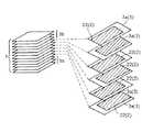
この実施形態では、積層セラミックコンデンサの製造工程において、図1に示すように、セラミック素子(電子部品素子)1中に、複数の内部電極2がセラミック層3を介して積層、配設され、かつ、セラミック層3を介して互いに対向する内部電極2が交互にセラミック素子(電子部品素子)1の逆側の端面に引き出されて、セラミック素子1の両端面に形成された一対の外部電極4に接続された構造を有する積層セラミックコンデンサ(電子部品)10を製造する場合を例にとって説明する。
【0013】
(1)電子部品素子(セラミック素子)の作製
図2に示すように、複数の内部電極2がセラミック層(誘電体層)3を介して積層、配設され、かつ、セラミック層3を介して互いに対向する内部電極2が交互に逆側の端面(一方の端面1a,及び他方の端面1b)に引き出された構造を有する電子部品素子(セラミック素子)1を作製した。
【0014】
具体的には、図3に部分的に示すように、セラミック層(誘電体層)3となる誘電体セラミックグリーンシート3a上に、Ni粉末を導電成分とする導体ペーストを印刷塗布することにより、内部電極2となる内部電極パターン22を形成した後、各誘電体セラミックグリーンシート3aと、電極パターンの配設されていないセラミックグリーンシート(外層用シート)3bを、内部電極層2が互いに対向するように積層・熱圧着し、製品(積層セラミックコンデンサ)の形状、寸法に応じて裁断した後、所定の条件で焼成することにより、図2に示すような焼結済みのセラミック素子1を作製した。
【0015】
(2)外部電極の形成
それから、バレル研磨を行って、セラミック素子1の端面1a,1bに内部電極2を確実に露出させ、ディッピング工法によって、導電ペーストをセラミック素子1の端面1a,1bを含む領域に塗布した。
【0016】
(3)一次熱処理及び二次熱処理
次に、表1に示すような条件で、熱処理温度、雰囲気中の酸素濃度、熱処理時間を変化させて一次熱処理を行った。
それから、一次熱処理が行われたセラミック素子を常温に戻した後、表1に示すような条件で、熱処理温度、雰囲気中の酸素濃度、熱処理時間を変化させて二次熱処理を行い、図1に示すような構造を有する積層セラミックコンデンサ10を得た。
【0017】
(4)耐湿性試験
そして、得られた積層セラミックコンデンサ10について、70℃、相対湿度95%、定格電圧で1000時間の耐湿負荷試験を行って、耐湿性を調べた。その結果を表1に併せて示す。
【0018】
【表1】
表1に示すように、熱処理温度850℃、酸素濃度100ppm、熱処理時間5分間の条件で熱処理(一次熱処理)しただけで、二次熱処理を行っていない試料番号1の試料の場合、図4(a)に示すように、空隙又はガラス層11に遮られて、金属の相互拡散による接合部分(接合領域)Aが細くしか形成されず、内部電極2と外部電極4の接合部分(接合領域)Aと、セラミック層3との隙間などからの水分の侵入を抑制する効果が不十分になり、耐湿負荷試験において、72個の試料中15個の試料に不良が発生した。
【0020】
また、熱処理温度850℃、酸素濃度100ppm、熱処理時間5分間の条件で一次熱処理した後、常温に戻し、再び、熱処理温度850℃、酸素濃度100ppm、熱処理時間5分間の条件(一次熱処理の条件と同じ条件)で二次熱処理した試料番号2の試料の場合、図4(b)に示すように、空隙又はガラス層11に遮られて、金属の相互拡散による接合部分(接合領域)Aがそれほど太くは形成されず、内部電極2と外部電極4の接合部分(接合領域)Aと、セラミック層3との隙間などからの水分の侵入を抑制する効果が不十分になり、耐湿負荷試験において、72個の試料中15個の試料に不良が発生した。
【0021】
これに対して、熱処理温度850℃、酸素濃度100ppm、熱処理時間5分間の条件で一次熱処理した後、常温に戻し、再び、熱処理温度750℃、酸素濃度50ppm、熱処理時間30分間の条件(一次熱処理工程におけるよりも低い熱処理温度、低い酸素濃度、長い熱処理時間の条件)で二次熱処理した試料番号3の試料(本発明の実施形態の試料)の場合、図4(c)に示すように、内部電極2と外部電極4との間の空隙又はガラス層11中に内部電極材料(Ni)が析出し、内部電極2(あるいは内部電極2と外部電極4の接合部分(接合領域)A)とセラミック素子1の隙間が塞がれるため、耐湿性が向上し、耐湿負荷試験において、72個の試料中、不良が発生したものはなかった。
【0022】
また、表2に示すような条件で、熱処理温度、雰囲気中の酸素濃度、熱処理時間を変化させて一次熱処理を行うとともに、一次熱処理が行われたセラミック素子を常温に戻した後、熱処理温度、雰囲気中の酸素濃度、熱処理時間を表2に示すような条件で変化させて二次熱処理を行った。
そして、得られた積層セラミックコンデンサについて、70℃、相対湿度95%、定格電圧で1000時間の耐湿負荷試験を行って、耐湿性を調べた。その結果を表2に併せて示す。
【0023】
【表2】
表2に示すように、一次熱処理と二次熱処理における熱処理温度が同じである試料番号4(一次熱処理工程の熱処理温度850℃、酸素濃度100ppm、熱処理時間5min、二次熱処理工程の熱処理温度850℃、酸素濃度50ppm、熱処理時間30min)では、良好な耐湿性を得ることができなかった。
【0025】
また、一次熱処理と二次熱処理における酸素濃度が同じである試料番号5(一次熱処理工程の熱処理温度850℃、酸素濃度100ppm、熱処理時間5min、二次熱処理工程の熱処理温度750℃、酸素濃度100ppm、熱処理時間30min)でも、良好な耐湿性を得ることができなかった。
【0026】
また、一次熱処理と二次熱処理における熱処理時間が同じである試料番号6(一次熱処理工程の熱処理温度850℃、酸素濃度100ppm、熱処理時間5min、二次熱処理工程の熱処理温度750℃、酸素濃度50ppm、熱処理時間5min)でも、良好な耐湿性を得ることができなかった。
【0027】
また、試料番号3(本発明の要件を満たす試料)に比べて、二次熱処理における熱処理温度を上げた試料番号7(一次熱処理工程の熱処理温度850℃、酸素濃度100ppm、熱処理時間5min、二次熱処理工程の熱処理温度800℃、酸素濃度50ppm、熱処理時間30min)では、試料番号3よりはいくらか劣るが一応実用可能な耐湿性を確保することができた。
【0028】
また、試料番号3(本発明の要件を満たす試料)に比べて、二次熱処理における酸素濃度を上げた試料番号8(一次熱処理工程の熱処理温度850℃、酸素濃度100ppm、熱処理時間5min、二次熱処理工程の熱処理温度750℃、酸素濃度80ppm、熱処理時間30min)では、試料番号3よりはいくらか劣るが一応実用可能な耐湿性を確保することができた。
【0029】
また、試料番号3(本発明の要件を満たす試料)に比べて、二次熱処理における熱処理時間を15分と短くした試料番号9(一次熱処理工程の熱処理温度850℃、酸素濃度100ppm、熱処理時間5min、二次熱処理工程の熱処理温度750℃、酸素濃度50ppm、熱処理時間15min)では、試料番号3よりはいくらか劣るが一応実用可能な耐湿性を確保することができた。
以上の結果より、本発明の方法によれば、電子部品の耐湿性を向上させることが可能になることがわかる。
【0030】
なお、上記実施形態では、積層セラミックコンデンサを例にとって説明したが、本発明は積層セラミックコンデンサに限られるものではなく、積層インダクタ、積層バリスタなど、セラミック素子中に配設された内部電極がセラミック素子の端面に引き出され、該端面に配設された外部電極に接続された構造を有する種々の電子部品を製造する場合に適用することが可能である。
【0031】
本発明はさらにその他の点においても上記実施形態に限定されるものではなく、発明の範囲内において種々の応用、変形を加えることが可能である。
【0032】
【発明の効果】
上述のように、本発明(請求項1)の電子部品の製造方法は、セラミック素子の、Ni又はNiを主成分とする材料からなる内部電極が引き出された端面を含む領域に導電ペーストを塗布し、熱処理温度、熱処理雰囲気中の酸素濃度、及び、熱処理時間を、(a)熱処理温度を750〜950℃、(b)熱処理雰囲気中の酸素濃度を50〜100ppm、(c)熱処理時間を5〜60minの条件に制御して熱処理(一次熱処理)を行い、導電ペーストを焼き付けてCu又はCuを主成分とする材料からなる外部電極を形成した後、セラミック素子を常温に戻した後、セラミック素子を、(a’)熱処理温度を一次熱処理の熱処理温度よりも50〜100℃低くし、(b’)熱処理雰囲気中の酸素濃度を一次熱処理の酸素濃度よりも20〜50 ppm低くし、(c’)熱処理時間を一次熱処理の熱処理時間よりも10〜25min長くした条件で、二次熱処理を行うようにしているので、内部電極とCu又はCuを主成分とする材料からなる外部電極の接合部分に内部電極を構成する金属(Ni)を多く析出させることが可能になり、水分に対するシール性を向上させることが可能になる。
【図面の簡単な説明】
【図1】 本発明の一実施形態にかかる電子部品の製造方法により製造される積層セラミックコンデンサ(電子部品)の構成を示す断面図である。
【図2】 本発明の電子部品の製造方法の一工程において形成されるセラミック素子(電子部品素子)を示す断面図である。
【図3】 本発明の電子部品の製造方法の一工程において形成されるセラミック素子(電子部品素子)の分解斜視図である。
【図4】 (a)は比較例の試料の内部電極と外部電極の接合部分(接合領域)の形状を模式的に示す断面図、(b)は他の比較例の試料の内部電極と外部電極の接合部分(接合領域)の形状を模式的に示す断面図、(c)は本発明の一実施形態にかかる方法により製造された試料の内部電極と外部電極の接合部分(接合領域)の形状を模式的に示す断面図である。
【符号の説明】
1 セラミック素子(電子部品素子)
1a,1b セラミック素子の端面
2 内部電極
3 セラミック層(誘電体層)
3a 誘電体セラミックグリーンシート
3b セラミックグリーンシート(外層用シート)
4 外部電極
10 積層セラミックコンデンサ(電子部品)
11 空隙又はガラス層
22 内部電極パターン
A 接合部分(接合領域)[0001]
BACKGROUND OF THE INVENTION
The present invention relates to a method of manufacturing an electronic component, and more specifically, an electronic device having a structure in which an internal electrode disposed in a ceramic element is drawn out to an end face of the ceramic element and connected to an external electrode disposed on the end face. The present invention relates to a part manufacturing method.
[0002]
[Prior art and problems to be solved by the invention]
As shown in FIG. 1, a surface mount type multilayer
[0003]
When the multilayer ceramic capacitor (electronic component) 10 having such a structure is manufactured, the
[0004]
However, in the multilayer ceramic capacitor (electronic component) 10 manufactured by the above-described conventional method, the metal constituting each of the
[0005]
The above-mentioned problem is not limited to the multilayer ceramic capacitor, and internal electrodes such as multilayer inductors and multilayer varistors disposed in the ceramic element are drawn out to the end face of the ceramic element and external electrodes disposed on the end face. This applies to an electronic component having a structure connected to.
[0006]
The present invention solves the above-described problem, and can prevent moisture from entering from a joint portion (such as a gap between the joint portion and the ceramic layer) between the internal electrode and the external electrode, and has high reliability. It is an object of the present invention to provide an electronic component manufacturing method capable of efficiently manufacturing an electronic component.
[0007]
[Means for Solving the Problems]
In order to achieve the above object, a method of manufacturing an electronic component according to the present invention (Claim 1) includes:
An internal electrode made ofNi or a material containing Ni as a main component disposed in the ceramic element is drawn out to an end face of the ceramic element,and an external electrode made of Cu or a material containing Cu as a main ingredient is provided on the end face. A method of manufacturing an electronic component having a structure connected to an electrode,
Applying a conductive paste to a region including the end face from which the internal electrode of the ceramic element is drawn,
(a) The heat treatment temperature is 750 to 950 ° C.
(b) the oxygen concentration in the heat treatment atmosphere is 50 to 100 ppm,
(c) Heat treatment time is 5 to 60 min
A primary heat treatment step of baking the conductive paste by performing heat treatment under the conditions of
Returning the ceramic element subjected to the primary heat treatment to room temperature;
The ceramic element,
(a ′) the heat treatment temperature is lower by 50 to 100 ° C. than the heat treatment temperature of the primary heat treatment,
(b ′) The oxygen concentration in the heat treatment atmosphere is 20 to 50 ppm lower than the oxygen concentration in the primary heat treatment,
and (c ′) a secondary heat treatment step in which the heat treatment time is 10 to 25 minutes longer than the heat treatment time of the primary heat treatment, and the heat treatment is performed under the heat treatment conditions that satisfy each condition.
[0008]
The conductive paste is applied to the region including the end face from which the internal electrode of the ceramic element is drawn,(a) the heat treatment temperature is 750 to 950 ° C., (b) the oxygen concentration in the heat treatment atmosphere is 50 to 100 ppm, and (c) the heat treatment time. Is controlled to a condition of 5to 60 min , heat treatment (primary heat treatment) is performed, the conductive paste is baked, the ceramic element is returned to room temperature, and then the ceramic elements are converted into the above (a ′), (b ′), By performing a secondary heat treatment under the condition of (c ′), a large amount of the metal constituting the internal electrode is deposited at the joint between the internal electrode and the external electrode made of Cu or Cu as a main component. It becomes possible to improve the sealing property against moisture.
[0009]
In the primary heat treatment step, the heat treatment temperature is 750 to 950 ° C., the oxygen concentration in the heat treatment atmosphere is 50 to 100 ppm, the heat treatment time is 5 to 60 minutes, and in the secondary heat treatment step, as defined in claim 1 The heat treatment temperature is 50 to 100 ° C. lower than the heat treatment temperature of the primary heat treatment, the oxygen concentration in the heat treatment atmosphere is 20 to 50 ppm lower than the oxygen concentration of the primary heat treatment, and the heat treatment time is 10 to 10 times lower than the heat treatment time of the primary heat treatment. When the length is increased by 25 minutes, a large amount of metal(Ni) constituting the internal electrode is deposited at the joint betweenthe internal electrode andthe external electrode made of Cu or Cu as a main component, thereby improving the sealing performance against moisture. It becomes possible to make it.
[0010]
The reason why the heat treatment temperature in the secondary heat treatment step is lowered by 50 to 100 ° C. compared to the heat treatment temperature in the primary heat treatment step is to control the amount of precipitation of the metal constituting the internal electrode. That is, when the heat treatment temperature in the secondary heat treatment step is equal to or higher than the heat treatment temperature in the primary heat treatment step, a large amount of metal constituting the internal electrode is precipitated in the secondary heat treatment step. And the internal electrode protrudes to form a cavity between the external electrode and the electronic component element. On the other hand, if the heat treatment temperature in the secondary heat treatment step is too low, precipitation of the metal constituting the internal electrode is reduced, and sufficient sealing performance against moisture cannot be obtained.
[0011]
The reason why the oxygen concentration in the secondary heat treatment step is lowered by 20 to 50 ppm compared to the oxygen concentration in the primary heat treatment step is to control the amount of deposited metal constituting the internal electrode. That is, if the oxygen concentration in the secondary heat treatment step is equal to or higher than the oxygen concentration in the primary heat treatment step, precipitation of the metal constituting the internal electrode is reduced, and sufficient sealing performance against moisture cannot be obtained. Conversely, if the oxygen concentration in the secondary heat treatment step is too low, the ceramic layer is reduced and desired characteristics cannot be obtained.
Furthermore, the reason why the heat treatment time of the secondary heat treatment step is made 10 to 25 minutes longer than the heat treatment time of the primary heat treatment step is to control the deposition amount of the metal constituting the internal electrode. When the heat treatment time in the secondary heat treatment step is set to be equal to or less than the heat treatment time in the primary heat treatment step, precipitation of the metal constituting the internal electrode is reduced, and sufficient sealing performance against moisture cannot be obtained. Conversely, if the heat treatment time in the secondary heat treatment step is too long, a large amount of the metal constituting the internal electrode will be precipitated in the secondary heat treatment step, whereby the internal electrode protrudes from the end face of the electronic component element, The protrusion creates a cavity between the external electrode and the electronic component element.
[0012]
DETAILED DESCRIPTION OF THE INVENTION
Hereinafter, embodiments of the present invention will be shown and the features thereof will be described in more detail.
In this embodiment, in the manufacturing process of a multilayer ceramic capacitor, as shown in FIG. 1, a plurality of
[0013]
(1) Production of Electronic Component Element (Ceramic Element) As shown in FIG. 2, a plurality of
[0014]
Specifically, as shown partially in FIG. 3, by applying a conductive paste containing Ni powder as a conductive component on a dielectric ceramic
[0015]
(2) Formation of external electrode Then, barrel polishing is performed so that the
[0016]
(3) Primary heat treatment and secondary heat treatment Next, the primary heat treatment was performed under the conditions shown in Table 1 while changing the heat treatment temperature, the oxygen concentration in the atmosphere, and the heat treatment time.
Then, after returning the ceramic element subjected to the primary heat treatment to room temperature, the secondary heat treatment was performed under the conditions shown in Table 1 by changing the heat treatment temperature, the oxygen concentration in the atmosphere, and the heat treatment time. A multilayer
[0017]
(4) Moisture resistance test The obtained multilayer
[0018]
[Table 1]
As shown in Table 1, in the case of the sample of sample number 1 which was just heat-treated (primary heat-treatment) under conditions of a heat-treatment temperature of 850 ° C., an oxygen concentration of 100 ppm and a heat-treatment time of 5 minutes, As shown to a), it is obstruct | occluded by the space | gap or the
[0020]
Also, after the primary heat treatment under the conditions of a heat treatment temperature of 850 ° C., an oxygen concentration of 100 ppm and a heat treatment time of 5 minutes, the temperature is returned to room temperature, and again the conditions of the heat treatment temperature of 850 ° C., the oxygen concentration of 100 ppm and the heat treatment time of 5 minutes (the conditions of the primary heat treatment) In the case of the sample No. 2 subjected to the secondary heat treatment under the same conditions), as shown in FIG. 4 (b), the gap or the
[0021]
On the other hand, after the primary heat treatment under the conditions of a heat treatment temperature of 850 ° C., an oxygen concentration of 100 ppm and a heat treatment time of 5 minutes, the temperature is returned to room temperature, and again the conditions of the heat treatment temperature of 750 ° C., the oxygen concentration of 50 ppm and the heat treatment time of 30 minutes (primary heat treatment). In the case of the sample No. 3 (sample of the embodiment of the present invention) subjected to secondary heat treatment at a lower heat treatment temperature, lower oxygen concentration, and longer heat treatment time conditions than in the process, as shown in FIG. The internal electrode material (Ni) is deposited in the gap between the
[0022]
Further, under the conditions shown in Table 2, the primary heat treatment was performed by changing the heat treatment temperature, the oxygen concentration in the atmosphere, and the heat treatment time, and after returning the ceramic element subjected to the primary heat treatment to room temperature, the heat treatment temperature, Secondary heat treatment was performed by changing the oxygen concentration in the atmosphere and the heat treatment time under the conditions shown in Table 2.
The obtained multilayer ceramic capacitor was subjected to a humidity resistance load test at 70 ° C., a relative humidity of 95%, and a rated voltage for 1000 hours to examine the moisture resistance. The results are also shown in Table 2.
[0023]
[Table 2]
As shown in Table 2, Sample No. 4 having the same heat treatment temperature in the primary heat treatment and the secondary heat treatment (heat treatment temperature of the primary heat treatment step 850 ° C., oxygen concentration 100 ppm, heat treatment time 5 min, heat treatment temperature of the secondary heat treatment step 850 ° C. When the oxygen concentration was 50 ppm and the heat treatment time was 30 minutes, good moisture resistance could not be obtained.
[0025]
Sample No. 5 having the same oxygen concentration in the primary heat treatment and the secondary heat treatment (heat treatment temperature in the primary heat treatment step 850 ° C., oxygen concentration 100 ppm, heat treatment time 5 min, heat treatment temperature in the secondary heat treatment step 750 ° C., oxygen concentration 100 ppm, Even at a heat treatment time of 30 minutes, good moisture resistance could not be obtained.
[0026]
Sample No. 6 having the same heat treatment time in the primary heat treatment and the secondary heat treatment (heat treatment temperature in the primary heat treatment step 850 ° C., oxygen concentration 100 ppm, heat treatment time 5 min, heat treatment temperature in the secondary heat treatment step 750 ° C., oxygen concentration 50 ppm, Even with a heat treatment time of 5 minutes, good moisture resistance could not be obtained.
[0027]
Sample No. 7 (heat treatment temperature of 850 ° C. in primary heat treatment step, oxygen concentration of 100 ppm, heat treatment time of 5 min, secondary heat treatment temperature increased in the secondary heat treatment as compared with sample No. 3 (sample satisfying the requirements of the present invention) At a heat treatment temperature of 800 ° C., an oxygen concentration of 50 ppm, and a heat treatment time of 30 minutes in the heat treatment step, it was possible to secure practically usable moisture resistance although it was somewhat inferior to Sample No. 3.
[0028]
Sample number 8 (heat treatment temperature 850 ° C., oxygen concentration 100 ppm, heat treatment time 5 min, secondary heat treatment in the primary heat treatment step) increased in oxygen concentration in the secondary heat treatment as compared with sample number 3 (sample satisfying the requirements of the present invention) At a heat treatment temperature of 750 ° C., an oxygen concentration of 80 ppm, and a heat treatment time of 30 minutes in the heat treatment step, it was possible to secure practically usable moisture resistance although it was somewhat inferior to Sample No. 3.
[0029]
Sample No. 9 (heat treatment temperature of 850 ° C., oxygen concentration of 100 ppm, heat treatment time of 5 min in the primary heat treatment step), which is shorter than the sample number 3 (sample satisfying the requirements of the present invention) in the secondary heat treatment, is 15 minutes. In the secondary heat treatment step, the heat treatment temperature of 750 ° C., the oxygen concentration of 50 ppm, and the heat treatment time of 15 minutes were somewhat inferior to those of Sample No. 3, but it was possible to ensure practically usable moisture resistance.
From the above results, it can be seen that according to the method of the present invention, the moisture resistance of the electronic component can be improved.
[0030]
In the above embodiment, a multilayer ceramic capacitor has been described as an example. However, the present invention is not limited to a multilayer ceramic capacitor, and internal electrodes disposed in a ceramic element such as a multilayer inductor and a multilayer varistor are ceramic elements. The present invention can be applied to the manufacture of various electronic components having a structure that is drawn out to the end face of the first electrode and connected to an external electrode disposed on the end face.
[0031]
The present invention is not limited to the above embodiment in other points, and various applications and modifications can be made within the scope of the invention.
[0032]
【The invention's effect】
As described above, in the method for manufacturing an electronic component according to the present invention (Claim 1), the conductive paste is applied to the region of the ceramic element including the end facefrom which the internal electrode made ofNi or Ni-based material is drawn. The heat treatment temperature, the oxygen concentration in the heat treatment atmosphere, and the heat treatment time,(a) the heat treatment temperature is 750 to 950 ° C., (b) the oxygen concentration in the heat treatment atmosphere is 50 to 100 ppm, and (c) the heat treatment time is 5 Heat treatment (primary heat treatment) is performedunder a condition of˜60 min , the conductive paste is baked to form an external electrode made of a material containing Cu or Cu as a main component, the ceramic element is returned to room temperature, and then the ceramic element (A ′) the heat treatment temperature is 50 to 100 ° C. lower than the heat treatment temperature of the primary heat treatment, (b ′) the oxygen concentration in the heat treatment atmosphere is 20 to 50 ppm lower than the oxygen concentration of the primary heat treatment, and (c ')Heat treatment Since the secondary heat treatment is performed under the condition that the interval is 10-25 minutes longer than the heat treatment time of the primary heat treatment, the internal electrode is connected to the joint portion between the internal electrode and the external electrode made of Cu or Cu as a main component. It is possible to deposit a large amount of the metal(Ni) constituting the material, and to improve the sealing performance against moisture.
[Brief description of the drawings]
FIG. 1 is a cross-sectional view showing a configuration of a multilayer ceramic capacitor (electronic component) manufactured by an electronic component manufacturing method according to an embodiment of the present invention.
FIG. 2 is a cross-sectional view showing a ceramic element (electronic component element) formed in one step of the electronic component manufacturing method of the present invention.
FIG. 3 is an exploded perspective view of a ceramic element (electronic component element) formed in one step of the electronic component manufacturing method of the present invention.
4A is a cross-sectional view schematically showing the shape of a joined portion (joined region) between an internal electrode and an external electrode of a sample of a comparative example, and FIG. 4B is an internal electrode and an external of a sample of another comparative example. Sectional drawing which shows the shape of the junction part (joint area | region) of an electrode typically, (c) is the junction part (joint area | region) of the internal electrode and external electrode of the sample which were manufactured by the method concerning one Embodiment of this invention. It is sectional drawing which shows a shape typically.
[Explanation of symbols]
1 Ceramic element (electronic component element)
1a, 1b End face of
3a Dielectric ceramic
4
11 Gap or
Claims (1)
Translated fromJapanese前記セラミック素子の内部電極が引き出された端面を含む領域に、導電ペーストを塗布し、
(a)熱処理温度を750〜950℃、
(b)熱処理雰囲気中の酸素濃度を50〜100ppm、
(c)熱処理時間を5〜60min
の条件に制御して熱処理を行うことにより、導電ペーストを焼き付ける一次熱処理工程と、
前記一次熱処理が行われた前記セラミック素子を常温に戻す工程と、
前記セラミック素子を、
(a’)熱処理温度を一次熱処理の熱処理温度よりも50〜100℃低くし、
(b’)熱処理雰囲気中の酸素濃度を一次熱処理の酸素濃度よりも20〜50 ppm低くし、
(c’)熱処理時間を一次熱処理の熱処理時間よりも10〜25min長くすること
の各条件を満たす熱処理条件下で熱処理する二次熱処理工程と
を具備することを特徴とする電子部品の製造方法。An internal electrode made ofNi or a material containing Ni as a main component disposed in the ceramic element is drawn out to an end face of the ceramic element,and an external electrode made of Cu or a material containing Cu as a main ingredient is provided on the end face. A method of manufacturing an electronic component having a structure connected to an electrode,
Applying a conductive paste to a region including the end face from which the internal electrode of the ceramic element is drawn,
(a) The heat treatment temperature is 750 to 950 ° C.
(b) the oxygen concentration in the heat treatment atmosphere is 50 to 100 ppm,
(c) Heat treatment time is 5-60 min
A primary heat treatment step of baking the conductive paste by controlling the conditions of
Returning the ceramic element subjected to the primary heat treatment to room temperature;
The ceramic element,
(a ′) the heat treatment temperature is lower by 50 to 100 ° C. than the heat treatment temperature of the primary heat treatment,
(b ′) The oxygen concentration in the heat treatment atmosphere is 20 to 50 ppm lower than the oxygen concentration in the primary heat treatment,
and (c ′) a secondary heat treatment step of performing a heat treatment under a heat treatment condition that satisfies each of the conditions that the heat treatment time is 10 to 25 minutes longer than the heat treatment time of the primary heat treatment.
Priority Applications (1)
| Application Number | Priority Date | Filing Date | Title |
|---|---|---|---|
| JP2002234782AJP4300770B2 (en) | 2002-08-12 | 2002-08-12 | Manufacturing method of electronic parts |
Applications Claiming Priority (1)
| Application Number | Priority Date | Filing Date | Title |
|---|---|---|---|
| JP2002234782AJP4300770B2 (en) | 2002-08-12 | 2002-08-12 | Manufacturing method of electronic parts |
Publications (2)
| Publication Number | Publication Date |
|---|---|
| JP2004079618A JP2004079618A (en) | 2004-03-11 |
| JP4300770B2true JP4300770B2 (en) | 2009-07-22 |
Family
ID=32019491
Family Applications (1)
| Application Number | Title | Priority Date | Filing Date |
|---|---|---|---|
| JP2002234782AExpired - Fee RelatedJP4300770B2 (en) | 2002-08-12 | 2002-08-12 | Manufacturing method of electronic parts |
Country Status (1)
| Country | Link |
|---|---|
| JP (1) | JP4300770B2 (en) |
Cited By (1)
| Publication number | Priority date | Publication date | Assignee | Title |
|---|---|---|---|---|
| US10134533B2 (en) | 2015-07-16 | 2018-11-20 | Murata Manufacturing Co., Ltd. | Multilayer ceramic capacitor and method for making multilayer ceramic capacitor |
Families Citing this family (7)
| Publication number | Priority date | Publication date | Assignee | Title |
|---|---|---|---|---|
| JP5180753B2 (en)* | 2008-09-26 | 2013-04-10 | Tdk株式会社 | Ceramic multilayer electronic component and manufacturing method thereof |
| JP2011049351A (en)* | 2009-08-27 | 2011-03-10 | Kyocera Corp | Laminated ceramic capacitor |
| JP2012019159A (en)* | 2010-07-09 | 2012-01-26 | Tdk Corp | Ceramic electronic component |
| JP5998785B2 (en)* | 2012-09-19 | 2016-09-28 | Tdk株式会社 | Laminated electronic components |
| DE102013106810A1 (en)* | 2013-06-28 | 2014-12-31 | Epcos Ag | Method for producing a multilayer varistor component and multilayer varistor component |
| JP7396225B2 (en)* | 2020-07-30 | 2023-12-12 | Tdk株式会社 | semiconductor ceramic electronic components |
| JP2023044364A (en)* | 2021-09-17 | 2023-03-30 | 太陽誘電株式会社 | Multilayer ceramic electronic component |
- 2002
- 2002-08-12JPJP2002234782Apatent/JP4300770B2/ennot_activeExpired - Fee Related
Cited By (1)
| Publication number | Priority date | Publication date | Assignee | Title |
|---|---|---|---|---|
| US10134533B2 (en) | 2015-07-16 | 2018-11-20 | Murata Manufacturing Co., Ltd. | Multilayer ceramic capacitor and method for making multilayer ceramic capacitor |
Also Published As
| Publication number | Publication date |
|---|---|
| JP2004079618A (en) | 2004-03-11 |
Similar Documents
| Publication | Publication Date | Title |
|---|---|---|
| KR101721630B1 (en) | Ceramic electronic component and manufacturing method therefor | |
| US6377439B1 (en) | Electronic multilayer ceramic component | |
| JP5483498B2 (en) | Multilayer ceramic electronic component and manufacturing method thereof | |
| KR102029469B1 (en) | Multilayered ceramic electronic component and fabricating method thereof | |
| JP5971236B2 (en) | Ceramic electronic components and glass paste | |
| US20170278634A1 (en) | Multilayer ceramic capacitor | |
| US9324483B2 (en) | Chip thermistor and method of manufacturing same | |
| CN112820543B (en) | Ceramic electronic component and method for manufacturing the same | |
| JP2023015365A (en) | Multilayer ceramic capacitor and manufacturing method thereof | |
| TW201323572A (en) | Conductive paste for external electrode, multilayer ceramic electronic component using the same, and method of manufacturing the same | |
| JP5960816B2 (en) | Multilayer ceramic capacitor | |
| JP4300770B2 (en) | Manufacturing method of electronic parts | |
| JP2943380B2 (en) | Multilayer ceramic capacitor and manufacturing method thereof | |
| JPH02135702A (en) | Lamination type varistor | |
| JPH04320017A (en) | Laminated ceramic capacitor and fabrication thereof, and external electrode paste used therefor | |
| JP6911754B2 (en) | Electronic components and multilayer ceramic capacitors | |
| JPH053134A (en) | Method for manufacturing external electrode of multilayer ceramic capacitor | |
| JP3918095B2 (en) | Multilayer ceramic electronic component and manufacturing method thereof | |
| JP2018056559A (en) | Multilayer varistor and method for producing the same | |
| JP4637440B2 (en) | Manufacturing method of ceramic element | |
| JP3716746B2 (en) | Multilayer ceramic electronic component and manufacturing method thereof | |
| JPH11214240A (en) | Laminated ceramic electronic component and their manufacture | |
| JP2005524226A (en) | PTC component and manufacturing method thereof | |
| JP2000077260A (en) | Laminated ceramic electronic component and its manufacture | |
| JP4360112B2 (en) | Manufacturing method of multilayer ceramic electronic component |
Legal Events
| Date | Code | Title | Description |
|---|---|---|---|
| A621 | Written request for application examination | Free format text:JAPANESE INTERMEDIATE CODE: A621 Effective date:20050706 | |
| A131 | Notification of reasons for refusal | Free format text:JAPANESE INTERMEDIATE CODE: A131 Effective date:20080129 | |
| A521 | Request for written amendment filed | Free format text:JAPANESE INTERMEDIATE CODE: A523 Effective date:20080331 | |
| A131 | Notification of reasons for refusal | Free format text:JAPANESE INTERMEDIATE CODE: A131 Effective date:20080805 | |
| A521 | Request for written amendment filed | Free format text:JAPANESE INTERMEDIATE CODE: A523 Effective date:20080929 | |
| TRDD | Decision of grant or rejection written | ||
| A01 | Written decision to grant a patent or to grant a registration (utility model) | Free format text:JAPANESE INTERMEDIATE CODE: A01 Effective date:20090331 | |
| A01 | Written decision to grant a patent or to grant a registration (utility model) | Free format text:JAPANESE INTERMEDIATE CODE: A01 | |
| FPAY | Renewal fee payment (event date is renewal date of database) | Free format text:PAYMENT UNTIL: 20120501 Year of fee payment:3 | |
| R150 | Certificate of patent or registration of utility model | Ref document number:4300770 Country of ref document:JP Free format text:JAPANESE INTERMEDIATE CODE: R150 Free format text:JAPANESE INTERMEDIATE CODE: R150 | |
| A61 | First payment of annual fees (during grant procedure) | Free format text:JAPANESE INTERMEDIATE CODE: A61 Effective date:20090413 | |
| FPAY | Renewal fee payment (event date is renewal date of database) | Free format text:PAYMENT UNTIL: 20120501 Year of fee payment:3 | |
| FPAY | Renewal fee payment (event date is renewal date of database) | Free format text:PAYMENT UNTIL: 20130501 Year of fee payment:4 | |
| FPAY | Renewal fee payment (event date is renewal date of database) | Free format text:PAYMENT UNTIL: 20130501 Year of fee payment:4 | |
| FPAY | Renewal fee payment (event date is renewal date of database) | Free format text:PAYMENT UNTIL: 20140501 Year of fee payment:5 | |
| LAPS | Cancellation because of no payment of annual fees |