JP4299863B2 - Manufacturing method of semiconductor device - Google Patents
Manufacturing method of semiconductor deviceDownload PDFInfo
- Publication number
- JP4299863B2 JP4299863B2JP2007011784AJP2007011784AJP4299863B2JP 4299863 B2JP4299863 B2JP 4299863B2JP 2007011784 AJP2007011784 AJP 2007011784AJP 2007011784 AJP2007011784 AJP 2007011784AJP 4299863 B2JP4299863 B2JP 4299863B2
- Authority
- JP
- Japan
- Prior art keywords
- opening
- degree
- closing
- semiconductor device
- manufacturing
- Prior art date
- Legal status (The legal status is an assumption and is not a legal conclusion. Google has not performed a legal analysis and makes no representation as to the accuracy of the status listed.)
- Expired - Fee Related
Links
Images


Classifications
- C—CHEMISTRY; METALLURGY
- C23—COATING METALLIC MATERIAL; COATING MATERIAL WITH METALLIC MATERIAL; CHEMICAL SURFACE TREATMENT; DIFFUSION TREATMENT OF METALLIC MATERIAL; COATING BY VACUUM EVAPORATION, BY SPUTTERING, BY ION IMPLANTATION OR BY CHEMICAL VAPOUR DEPOSITION, IN GENERAL; INHIBITING CORROSION OF METALLIC MATERIAL OR INCRUSTATION IN GENERAL
- C23C—COATING METALLIC MATERIAL; COATING MATERIAL WITH METALLIC MATERIAL; SURFACE TREATMENT OF METALLIC MATERIAL BY DIFFUSION INTO THE SURFACE, BY CHEMICAL CONVERSION OR SUBSTITUTION; COATING BY VACUUM EVAPORATION, BY SPUTTERING, BY ION IMPLANTATION OR BY CHEMICAL VAPOUR DEPOSITION, IN GENERAL
- C23C16/00—Chemical coating by decomposition of gaseous compounds, without leaving reaction products of surface material in the coating, i.e. chemical vapour deposition [CVD] processes
- C23C16/44—Chemical coating by decomposition of gaseous compounds, without leaving reaction products of surface material in the coating, i.e. chemical vapour deposition [CVD] processes characterised by the method of coating
- C23C16/4412—Details relating to the exhausts, e.g. pumps, filters, scrubbers, particle traps
- C—CHEMISTRY; METALLURGY
- C23—COATING METALLIC MATERIAL; COATING MATERIAL WITH METALLIC MATERIAL; CHEMICAL SURFACE TREATMENT; DIFFUSION TREATMENT OF METALLIC MATERIAL; COATING BY VACUUM EVAPORATION, BY SPUTTERING, BY ION IMPLANTATION OR BY CHEMICAL VAPOUR DEPOSITION, IN GENERAL; INHIBITING CORROSION OF METALLIC MATERIAL OR INCRUSTATION IN GENERAL
- C23C—COATING METALLIC MATERIAL; COATING MATERIAL WITH METALLIC MATERIAL; SURFACE TREATMENT OF METALLIC MATERIAL BY DIFFUSION INTO THE SURFACE, BY CHEMICAL CONVERSION OR SUBSTITUTION; COATING BY VACUUM EVAPORATION, BY SPUTTERING, BY ION IMPLANTATION OR BY CHEMICAL VAPOUR DEPOSITION, IN GENERAL
- C23C16/00—Chemical coating by decomposition of gaseous compounds, without leaving reaction products of surface material in the coating, i.e. chemical vapour deposition [CVD] processes
- C23C16/44—Chemical coating by decomposition of gaseous compounds, without leaving reaction products of surface material in the coating, i.e. chemical vapour deposition [CVD] processes characterised by the method of coating
- C23C16/455—Chemical coating by decomposition of gaseous compounds, without leaving reaction products of surface material in the coating, i.e. chemical vapour deposition [CVD] processes characterised by the method of coating characterised by the method used for introducing gases into reaction chamber or for modifying gas flows in reaction chamber
- C23C16/45523—Pulsed gas flow or change of composition over time
- C23C16/45525—Atomic layer deposition [ALD]
- C23C16/45527—Atomic layer deposition [ALD] characterized by the ALD cycle, e.g. different flows or temperatures during half-reactions, unusual pulsing sequence, use of precursor mixtures or auxiliary reactants or activations
Landscapes
- Chemical & Material Sciences (AREA)
- General Chemical & Material Sciences (AREA)
- Chemical Kinetics & Catalysis (AREA)
- Engineering & Computer Science (AREA)
- Materials Engineering (AREA)
- Mechanical Engineering (AREA)
- Metallurgy (AREA)
- Organic Chemistry (AREA)
- Chemical Vapour Deposition (AREA)
Description
Translated fromJapanese本発明は、半導体装置の製造方法に関し、更に詳しくは、原子層成長(以下、ALDと呼ぶ。ALD: Atomic Layer Deposition)法を利用して、半導体装置内に容量絶縁膜を成膜する技術の改良に関する。The present invention relatesto the productionhow the semiconductor device, and more particularly, atomic layer deposition (hereinafter, referred to as ALD .ALD: Atomic Layer Deposition) method using, for forming the capacitor insulating film in a semiconductor device It relates to technical improvements.
微細化技術の向上によりDRAMの高密度化が加速され、キャパシタに許容できる占有面積は減少している。一方、デバイス動作に必要な容量は維持する必要があり、世代が進むにつれて、シリンダ−を深くする等の構造(高アスペクト構造)が主流になっている。このような背景に対して従来のCVD(Chemical Vapor Deposition)法では、被覆性良く容量絶縁膜を形成することが困難になってきた。そこで近年、ALD法による成膜が行われている。ALD法は原子層毎に成膜する手法である。例えば非晶質酸化アルミニウム膜を成膜する場合には、図9に示す通り、アルミソースであるトリメチルアルミニウム(TMA)を導入するステップ(ステップB)と、酸化剤であるオゾン(O3)を導入するステップ(ステップE)とを交互に行う。また、それぞれのガス導入ステップの間には、気相中で反応しないように、真空引きステップ(ステップD及びG)と、不活性ガス(アルゴン(Ar)等)によるパージステップ(ステップA、C、F)とを行う。導入されたトリメチルアルミニウム(TMA)は、半導体基板の表面に吸着した材料のみが酸化されるため、基板表面の吸着量を最適化することで、高アスペクト構造でも緻密で良質な容量絶縁膜を形成することが可能となる。Improvement in miniaturization technology has accelerated the increase in the density of DRAMs, and the area occupied by capacitors has decreased. On the other hand, it is necessary to maintain the capacity necessary for device operation, and as generations progress, structures such as deeper cylinders (high aspect structures) have become mainstream. Against this background, it has become difficult to form a capacitive insulating film with good coverage by the conventional CVD (Chemical Vapor Deposition) method. Therefore, in recent years, film formation by the ALD method has been performed. The ALD method is a method for forming a film for each atomic layer. For example, when an amorphous aluminum oxide film is formed, as shown in FIG. 9, a step of introducing trimethylaluminum (TMA) as an aluminum source (Step B) and ozone (O3 ) as an oxidizing agent are performed. The step of introducing (Step E) is performed alternately. Between each gas introduction step, a evacuation step (steps D and G) and a purge step (steps A and C) with an inert gas (such as argon (Ar)) are performed so as not to react in the gas phase. , F). The introduced trimethylaluminum (TMA) oxidizes only the material adsorbed on the surface of the semiconductor substrate, so by optimizing the amount of adsorption on the surface of the substrate, a dense and high-quality capacitive insulating film is formed even in a high aspect structure It becomes possible to do.
一方、半導体産業は価格変動が激しく、競合他社との競争に打ち勝つためには、製造コストの低減が不可欠である。このため、半導体基板の大口径化の流れが加速しているものの、半導体基板の大口径化に伴い、基板全面において一様に成膜することが困難になりつつある。特に、半導体基板全面のシリンダー底部にまで一様に成膜するために上記ALD法を用いた場合には、シリンダー底部での気相反応物の表面吸着量を同一にする必要があり、充分過ぎるほど気相反応物を供給することで表面吸着量を飽和させるか、或いは、ガス供給が全面均一になるように制御して表面吸着量を飽和領域に達しない一定量にすることが必要である。 On the other hand, in the semiconductor industry, prices fluctuate drastically, and it is essential to reduce manufacturing costs in order to overcome competition with competitors. For this reason, although the flow of increasing the diameter of the semiconductor substrate is accelerating, it is becoming difficult to form a film uniformly over the entire surface of the substrate as the diameter of the semiconductor substrate increases. In particular, when the ALD method is used to form a film uniformly on the bottom of the cylinder on the entire surface of the semiconductor substrate, the surface adsorption amount of the gas phase reactant on the bottom of the cylinder needs to be the same, which is too much. It is necessary to saturate the surface adsorption amount by supplying the gas phase reactant, or to control the gas supply to be uniform over the entire surface so that the surface adsorption amount does not reach the saturation region. .
従来のALD装置の一例を図10に示す。図10では、形成する容量絶縁膜が非晶質酸化アルミニウム膜であり、非晶質酸化アルミニウムを形成するためのアルミソースとしてトリメチルアルミニウムを(TMA)、酸化剤としてオゾン(O3)をそれぞれ用いる。トリメチルアルミニウム(TMA)とオゾン(O3)は独立した導入管35及び36から、シャワーヘッド33を通って反応室(成膜室)31内に導入される。また各々の導入管35、36には、配管内部及び反応室31内を不活性ガスで置換できるように、アルゴン(Ar)の導入管が接続されている。また未反応ガスや反応生成物を排出するために排気管38が設けられ、この排気管38は図示しない真空排気設備に接続されている。An example of a conventional ALD apparatus is shown in FIG. In FIG. 10, the capacitor insulating film to be formed is an amorphous aluminum oxide film, and trimethylaluminum (TMA) is used as an aluminum source for forming amorphous aluminum oxide, and ozone (O3 ) is used as an oxidizing agent. . Trimethyl aluminum (TMA) and ozone (O 3) are introduced into the reaction chamber (film formation chamber) 31 through the
排気管38の途中には圧力制御用回転式バルブ39が設置され、その開閉度を調節することで、反応室31内の圧力は0.133〜13.3Paの間で調整できる。更に、反応室31にはステージヒーター34が設けられており、処理中の半導体基板32はステージヒーター34上に設置されることで成膜温度まで加熱される。成膜温度は、形成する容量絶縁膜の種類及び半導体基板の構造に合わせて、250〜500℃の範囲で任意に選択できる。試料搬入口37を通って反応室31内に半導体基板32が搬入された後、非晶質酸化アルミニウム膜の形成を開始する。成膜後の膜厚均一性は、真空度や成膜温度、ガス流量等を調整することで対応している。
ところで、上記ALD処理の各ステップで供給されるガスの最適供給量が異なる場合には、ガスの流れる方向がステップ毎に異なるため、半導体基板全面で一様に成膜できない場合がある。また半導体基板表面の膜厚が均一であっても面内で膜質が異なる場合もある。更に、上述したように高アスペクト構造化が加速されている現状では、例えばシリンダー上部での膜厚、膜質は同等であっても、シリンダー底部まで充分にガスが供給されず被覆性が低下することなどが起こり得る。このような問題を解決するために、充分すぎるほどの供給飽和状態を用いる場合には、図9におけるステップB(又はE)の設定時間を数10〜数100秒、場合によってはそれ以上に設定する必要があり、装置処理能力を極端に低下させる。そのため、ガスの流れを全面均一になるよう制御し、供給飽和状態を用いずとも良質な膜が形成できる半導体製造装置が必要であるが、従来のALD装置ではガスの流れを制御することは難しい。 By the way, when the optimal supply amount of the gas supplied in each step of the ALD process is different, the gas flow direction is different for each step, so that there is a case where the film cannot be uniformly formed on the entire surface of the semiconductor substrate. Even if the film thickness of the semiconductor substrate surface is uniform, the film quality may be different within the surface. Furthermore, as described above, in the current situation where the high aspect structure is accelerated, for example, even if the film thickness and film quality at the upper part of the cylinder are the same, the gas is not sufficiently supplied to the bottom of the cylinder and the coverage is reduced. Etc. can occur. In order to solve such a problem, when a supply saturation state that is too high is used, the set time of step B (or E) in FIG. 9 is set to several tens to several hundred seconds, and in some cases more than that. And the processing capacity of the apparatus is extremely reduced. Therefore, there is a need for a semiconductor manufacturing apparatus that can control the gas flow to be uniform over the entire surface and can form a high-quality film without using a supply saturation state, but it is difficult to control the gas flow with a conventional ALD apparatus. .
一例として、従来のALD装置の上面図と側面図を図11に示す。図中矢印で示したのは、ステップB(又はE)での成膜中のガスの流れる方向であり、矢印の本数でガスの流量を示している。理想的には、反応室31中央に排気管38を設置し、反応室31内部を真円にすることで、ガスは全方位均一に流れる。しかし、実際には反応室31中央にはステージヒーター34等、重要なユニットが存在し、排気管38は反応室31の中心から外れた位置に設置されることが多い。また反応室31内部も真円とはならず様々な凹凸があるためにガスの流れに偏りが発生する。このような問題を改善するための一例として、図12に示すように、遮蔽板50を反応室31に設置している装置もある。 As an example, a top view and a side view of a conventional ALD apparatus are shown in FIG. The arrows in the figure indicate the direction of gas flow during film formation in step B (or E), and the number of arrows indicates the gas flow rate. Ideally, the
遮蔽板50には、反応室31内でのガスの流れを調整するために孔径を変更した開口部が設けられ、ガスの流れを調整している。しかしながらこの構造はあくまで標準的な条件を用いた場合のみを想定しているため、標準条件から逸脱した条件を用いた場合には、やはりガスの流れに偏りが生じる。実際に遮蔽板50が設置された装置にて標準条件(条件A)で成膜した場合と、容量絶縁膜の膜質を最適にするため、標準条件から逸脱した条件(条件B)を用いた場合とについて、Al2O3膜における膜厚面内分布の傾向を測定した結果を図13(a)及び(b)に示す。標準条件(条件A)では同心円状に膜厚が変化しており、ガスが全方位均一に流れていることがわかる。しかし膜質を重視した条件(条件B)を用いた場合には、ガスの流れの偏りを反映し膜厚が変化している。このように容量絶縁膜の膜質を向上するために最適なガス供給量に設定した場合には、面内分布の均一性が崩れることがあり、それを許容できない場合には、膜質を低下させても面内均一性を向上させる条件を適用しなければならない。The
反応室内のガスの流れを均一化する技術としては、特許文献1に記載された半導体気相成長装置が知られている。該特許文献に記載の装置では、気相成長反応室に複数の排気管を設け、各排気管毎に排気量を調整するバルブを設けている。しかし、この特許文献に記載の半導体気相成長装置では、排気管に備える各バルブについての開閉度制御が成されていない。このため、この技術をALD装置に適用すると、容量絶縁膜の膜質を向上するために最適なガス供給量に設定した場合などのように、所定の標準条件を逸脱した場合には、再度バルブの開閉度調整が不可欠である。このため、成膜の処理能力が低下する。 As a technique for making the gas flow in the reaction chamber uniform, a semiconductor vapor phase growth apparatus described in Patent Document 1 is known. In the apparatus described in the patent document, a plurality of exhaust pipes are provided in the vapor phase growth reaction chamber, and a valve for adjusting the exhaust amount is provided for each exhaust pipe. However, in the semiconductor vapor phase growth apparatus described in this patent document, the degree of opening / closing control is not performed for each valve provided in the exhaust pipe. For this reason, when this technology is applied to an ALD apparatus, if the gas supply amount is set to an optimum value in order to improve the film quality of the capacitive insulating film, and if the predetermined standard condition is deviated, the valve It is essential to adjust the degree of opening and closing. For this reason, the processing capability of film formation decreases.
そこで、本発明の目的は、成膜における処理能力を低下させることなく、ALD法を用いた成膜時に、各ステップ毎にガスの流れを制御し高アスペクト構造での被覆性を向上させ、均質な成膜をウエハ全面及びシリンダー全体で得ることができる半導体製造装置を提供することにある。 Therefore, an object of the present invention is to improve the coverage in a high aspect structure by controlling the gas flow at each step during film formation using the ALD method without reducing the throughput in film formation. An object of the present invention is to provide a semiconductor manufacturing apparatus capable of obtaining an appropriate film formation on the entire wafer surface and the entire cylinder.
本発明の目的は、また、ALD法において成膜時に、各ステップ毎にガスの流れを制御し、高アスペクト構造での被覆性を向上させ、均質な絶縁膜を形成できる半導体装置の製造方法を提供することにある。 Another object of the present invention is to provide a method of manufacturing a semiconductor device capable of controlling the gas flow at each step during film formation in the ALD method, improving the coverage with a high aspect structure, and forming a homogeneous insulating film. It is to provide.
上記目的を達成するために、本発明の半導体製造装置は、気相反応物を交互に反応室に送り、半導体基板上に原子層レベルで成膜を行う枚葉式原子層成長(ALD)装置であって、
反応室内に配設され、前記半導体基板が設置されるステージと、
前記ステージの周辺に設けられ、排気量が個別に制御できる複数の排気管とを具備し、該排気管はそれぞれ、排気量を調整するためのバルブを備え、該バルブの開閉度が、該バルブの上流側に配置されて前記排気管内の真空度を計測する第1の真空計の計測値に依存して制御されることを特徴とする。In order to achieve the above object, a semiconductor manufacturing apparatus according to the present invention is a single-wafer atomic layer growth (ALD) apparatus in which vapor phase reactants are alternately sent to a reaction chamber to form a film on a semiconductor substrate at an atomic layer level. Because
A stage disposed in a reaction chamber and provided with the semiconductor substrate;
A plurality of exhaust pipes provided around the stage and capable of individually controlling the exhaust amount, each of the exhaust pipes being provided with a valve for adjusting the exhaust amount; It is controlled depending on the measured value of the 1st vacuum gauge which is arrange | positioned in the upstream and measures the degree of vacuum in the said exhaust pipe.
また、本発明の半導体装置の製造方法は、気相反応物を交互に反応室に送り、原子層レベルで成膜を順次に行う原子層成長(ALD)を用いて、半導体基板上にキャパシタの容量絶縁膜を形成する、半導体装置の製造方法において、
上記本発明の半導体製造装置を用い、容量絶縁膜の形成時に気相反応物の流れる方向を制御することを特徴とする。In addition, according to the method for manufacturing a semiconductor device of the present invention, a vapor-phase reactant is alternately sent to a reaction chamber, and a capacitor is formed on a semiconductor substrate using atomic layer growth (ALD) in which film formation is sequentially performed at an atomic layer level. In the method for manufacturing a semiconductor device, the capacitor insulating film is formed.
The semiconductor manufacturing apparatus of the present invention is used to control the flow direction of the gas phase reactant when forming the capacitive insulating film.
本発明の半導体製造装置及び方法によると、排気量が個別に制御できる複数の排気管によって反応室内のガスを排気することにより、標準条件を逸脱した場合にも、何れのステップにおいても、反応室内のガス流が制御できるので、半導体基板上に一様な厚みの容量絶縁膜の形成が可能になる。 According to the semiconductor manufacturing apparatus and method of the present invention, even if the standard condition is deviated by exhausting the gas in the reaction chamber by a plurality of exhaust pipes whose exhaust amount can be individually controlled, in any step Therefore, it is possible to form a capacitive insulating film having a uniform thickness on the semiconductor substrate.
本発明の半導体製造装置では、前記バルブが、圧力制御用回転式バルブであり、その開度が0度から90度の範囲で任意の値に制御されてもよい。また、この前記圧力制御用回転式バルブの開閉度が、前記反応室内の真空度を計測する第2の真空計の計測値に更に依存して制御されてもよい。 In the semiconductor manufacturing apparatus of the present invention, the valve may be a rotary valve for pressure control, and the opening degree may be controlled to an arbitrary value in the range of 0 degrees to 90 degrees. Further, the degree of opening and closing of the pressure control rotary valve may be controlled further depending on the measured value of the second vacuum gauge for measuring the degree of vacuum in the reaction chamber.
前記第2の真空計の計測値が所定の設定値になるように制御され、且つ、各排気管に流れ込む排気量が同じになるように前記圧力制御用回転式バルブの開閉度が個別に制御されてもよい。この場合、バルブの開閉度制御が簡素化できる。 The measured value of the second vacuum gauge is controlled to be a predetermined set value, and the opening / closing degree of the pressure control rotary valve is individually controlled so that the exhaust amount flowing into each exhaust pipe is the same. May be. In this case, valve opening / closing degree control can be simplified.
前記排気管はそれぞれ、排気量を調整するための圧力制御用回転式バルブと、前記圧力制御用回転式バルブをバイパスするバイパスラインとを具備してもよい。迅速な制御が可能になる。 Each of the exhaust pipes may include a pressure control rotary valve for adjusting an exhaust amount and a bypass line that bypasses the pressure control rotary valve. Rapid control is possible.
前記バイパスラインは、アイソレーションバルブを具備しており、該アイソレーションバルブの開閉が、前記第2の真空計の計測値に依存して制御されてもよい。この場合、制御が単純化できる。 The bypass line may include an isolation valve, and the opening and closing of the isolation valve may be controlled depending on the measurement value of the second vacuum gauge. In this case, the control can be simplified.
ALDの成膜に寄与するステップでは、前記アイソレーションバルブを閉じて圧力制御用回転式バルブにより気相反応物の流れを制御し、成膜に寄与しないステップでは、前記アイソレーションバルブを開放しバイパスラインを用いて排気してもよい。 In the step contributing to the film formation of ALD, the isolation valve is closed and the flow of the gas phase reactant is controlled by the rotary valve for pressure control. In the step not contributing to the film formation, the isolation valve is opened and bypassed. You may exhaust using a line.
前記アイソレーションバルブを開放しバイパスラインを用いて排気している間に圧力制御用回転式バルブの開閉度を次のステップの最適値に変更するよう制御してもよい。制御のスピードが向上する。 Control may be performed so that the degree of opening and closing of the pressure control rotary valve is changed to the optimum value in the next step while the isolation valve is opened and exhausted using the bypass line. The speed of control is improved.
本発明の半導体装置の製造方法では、前記容量絶縁膜を形成するプロセス条件作成時に、ALDの各ステップで気相反応物の流れを均一にするため、圧力制御用回転式バルブの開閉度最適化の手順を実施してもよい。 In the method of manufacturing a semiconductor device according to the present invention, when the process conditions for forming the capacitive insulating film are created, the degree of opening and closing of the pressure control rotary valve is optimized in order to make the flow of the gas phase reactant uniform in each step of ALD. You may implement the procedure of.
また、前記圧力制御用回転式バルブの開閉度最適化の手順で反応室に供給するガスは、実際の成膜に用いる気相反応物と同じであってもよい。正確な最適化が容易になる。 Further, the gas supplied to the reaction chamber in the procedure for optimizing the opening / closing degree of the pressure control rotary valve may be the same as the gas phase reactant used in the actual film formation. Accurate optimization is facilitated.
或いは、上記に代えて、前記圧力制御用回転式バルブの開閉度最適化の手順で供給するガスは、半導体製造装置に接続されている任意のガスを用いてもよい。開閉度最適化手順が簡素化される。 Alternatively, instead of the above, the gas supplied in the procedure for optimizing the opening / closing degree of the pressure control rotary valve may be any gas connected to the semiconductor manufacturing apparatus. Open / close optimization procedure is simplified.
また、前記容量絶縁膜形成時に圧力制御用回転式バルブの開閉度最適化の手順で決定された開閉度最適値を、各ステップの開閉度設定パラメータとして使用し、各ステップの切り替わるタイミングに合わせて圧力制御用回転式バルブの開閉度を変更してもよい。 Further, the opening / closing degree optimum value determined by the procedure for optimizing the opening / closing degree of the pressure control rotary valve at the time of forming the capacitive insulating film is used as the opening / closing degree setting parameter of each step, and in accordance with the timing of switching of each step. The degree of opening and closing of the pressure control rotary valve may be changed.
或いは、上記に代えて、前記容量絶縁膜形成時に、圧力制御用回転式バルブの開閉度を各ステップの切り替わるタイミングに合わせて、反応室に設置された真空計の計測値と、各排気管毎に設置された真空計の計測値とを用いて、開閉度を制御してもよい。 Alternatively, instead of the above, when the capacitive insulating film is formed, the opening / closing degree of the pressure control rotary valve is adjusted to the timing at which each step is switched, and the measured value of the vacuum gauge installed in the reaction chamber and each exhaust pipe The degree of opening and closing may be controlled using the measured value of the vacuum gauge installed in the.
更には、前記容量絶縁膜形成時に、圧力制御用回転式バルブの開閉度最適化の手順で決定された開閉度最適値を各ステップの開閉度設定パラメータとして使用し、各ステップの切り替わるタイミングに合わせて圧力制御用回転式バルブの開閉度を最適値まで変更した後、反応室に設置された真空計の計測値と各排気管毎に設置された真空計の計測値とを用いて、開閉度を制御してもよい。特に、正確な制御が可能になる。 Furthermore, when the capacitance insulating film is formed, the optimum degree of opening / closing determined by the procedure for optimizing the degree of opening / closing of the pressure control rotary valve is used as the opening / closing degree setting parameter of each step, and is matched with the timing of switching of each step. After changing the opening / closing degree of the pressure control rotary valve to the optimum value, the degree of opening / closing is determined using the measured value of the vacuum gauge installed in the reaction chamber and the measured value of the vacuum gauge installed for each exhaust pipe. May be controlled. In particular, accurate control becomes possible.
前記容量絶縁膜形成時の圧力制御用回転式バルブの開閉度の変更は、容量絶縁膜の成膜に寄与しないステップで行ってもよい。或いは、容量絶縁膜の成膜に寄与しないステップの前後のステップで行ってもよい。この場合、前記容量絶縁膜形成時の成膜に寄与しないステップの圧力制御用回転式バルブの開閉度を完全解放に設定してもよい。 The opening / closing degree of the pressure control rotary valve when forming the capacitive insulating film may be changed in a step that does not contribute to the formation of the capacitive insulating film. Alternatively, it may be performed in steps before and after the step that does not contribute to the formation of the capacitive insulating film. In this case, the degree of opening and closing of the pressure control rotary valve in a step that does not contribute to the film formation when the capacitive insulating film is formed may be set to be completely open.
また、前記容量絶縁膜形成時の成膜に寄与しないステップの圧力制御用回転式バルブの開閉度を、次のステップのバルブ開閉度最適値に設定してもよい。この場合、制御が迅速になる。 Further, the degree of opening / closing of the pressure control rotary valve in the step that does not contribute to the film formation when the capacitive insulating film is formed may be set to the valve opening degree optimum value in the next step. In this case, the control is quick.
以下、添付した図面を参照しながら、本発明の実施の形態を以下に詳述する。なお、全図を通して、同様な要素には同様な符号を付して示している。 Hereinafter, embodiments of the present invention will be described in detail with reference to the accompanying drawings. In addition, the same code | symbol is attached | subjected and shown to the same element through all the figures.
(第1の実施の形態)
図1は、本発明の第1の実施の形態に係る半導体製造装置におけるALD装置を示し、同図(a)はその上面図、同図(b)は図(a)のB−B線断面図である。本実施形態では、全ての成膜条件下においてガスの流れを全方位均一に制御できる容量絶縁膜形成が可能な半導体製造装置、特に枚様式原子層成長(ALD)装置の構造、及び、その容量絶縁膜形成方法について述べる。(First embodiment)
1A and 1B show an ALD apparatus in a semiconductor manufacturing apparatus according to a first embodiment of the present invention. FIG. 1A is a top view thereof, and FIG. 1B is a cross-sectional view taken along line BB in FIG. FIG. In this embodiment, the structure of a semiconductor manufacturing apparatus capable of forming a capacitive insulating film that can control the gas flow uniformly in all directions under all film forming conditions, particularly the structure of a single-layer atomic layer growth (ALD) apparatus, and its capacity An insulating film forming method will be described.
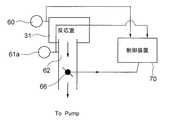
本実施形態におけるALD装置は、同じ径の排気管を最低2つ以上(図1の例では4本)具備し、全ての排気管62〜65は、その内部に、排気圧力調節用の真空計61a〜61dと、圧力制御用回転式バルブ66〜69とを備えている。排気管62〜65は、反応室31内又は反応室31外で、排気管38に集約されて、図示しない真空排気設備に接続されている。このとき集約される排気管は、図に示すように1本でも良いし、或いは、複数本でもよい。また、各排気管62〜65が集約されずに、それぞれ単独で真空排気設備に接続されてもよい。 The ALD apparatus according to the present embodiment includes at least two exhaust pipes having the same diameter (four in the example of FIG. 1), and all the
排気管62〜65の排気圧力は、各排気管に取り付けられている真空計61a〜61dの値が同一になるように、各圧力制御用回転式バルブ66〜69の開閉度を調節することで制御される。このとき、圧力制御用回転式バルブ66〜69の開閉度は、0〜90度の範囲で最適な値に設定される。例えば0度に設定されると、排気管は完全に閉塞した状態であり、90度に設定されると、排気管は完全に開放した状態になる。図2は、図1のALD装置の一部を模式的に示す系統図である。図2に示すように、反応室31内の真空度は真空計60でモニターされ、その計測値が制御装置70に送られる。更に排気管62の排気圧力をモニターする真空計61aの計測値も、同様に制御装置70に送られる。制御装置70は、真空計60の計測値が予め定められた設定圧力になるように制御すると共に、真空計61aの計測値が他の排気管をモニターする真空計61b〜61dの計測値と同じになるように、圧力制御用回転式バルブ66の開閉度を調節する。図2では、排気管62のみを図示しているが、他の排気管63〜65も、排気管62と同様に制御装置70を用いて制御している。 The exhaust pressure of the
通常、ALDプロセスは、図9に示すタイミングチャートに従って処理が進められる。ステップB及びEでは、ガスの流れが均一になるように制御することが重要である。一方、その他のステップでは、可能な限り速やかに反応室31内に残留する未反応ガス又は反応生成物を排出することが重要であり、このときには、ガスの流れを制御する必要はない。また、ステップB及びEでは、異なる材料を供給するため、最適なガスの流量が異なる。従って、複数の排気管を接続しても、圧力制御用回転式バルブ66〜69の開閉度を、全てのステップで同一に固定すると、ガスの流れを全方位均一にすることができない。つまり、各ステップ毎に最適バルブ開閉度に制御することが必要である。以下、同装置を用いた容量絶縁膜形成方法について詳述する。 Normally, the ALD process proceeds according to the timing chart shown in FIG. In steps B and E, it is important to control the gas flow to be uniform. On the other hand, in other steps, it is important to discharge the unreacted gas or reaction product remaining in the
第1の段階として、各ステップでのガスの流れを均一にするため、圧力制御用回転式バルブ66〜69の開閉度最適化を実施する。まず、容量絶縁膜の形成時に必要なパラメータ(成膜温度、反応室31の真空度等)を設定した後に、ステップB(又はE)で供給されるガス流量の総量と同量のガスを反応室31内に供給し、各配管の真空計61a〜61dの計測値が同じになるように、各排気管62〜65のバルブの開閉度を制御する。このとき、反応室31に供給するガスは、実際の成膜に用いる気相反応物(TMA又はO3)でもよく、或いは、アルゴンガス等の不活性ガスやO2等の、ALD装置に接続されている任意のガスで実施することも可能である。As a first stage, the degree of opening / closing of the pressure control
通常は、第1の段階ではアルゴンガス等の不活性ガスを用いる。また、反応室31内の真空度は、反応室31内をモニターする真空計60の値が、予め設定された値になるように制御される。反応室31内のガスの流れが均一になり、各排気管62〜65に取り付けられた真空計61a〜61dの計測値が同じになるバルブ開閉度を最適開閉度とする。図3にステップB及びEの最適開閉度の一例を示す。同図(a)は、回転式バルブの状態を示し、また、同図(b)はステップBにおける最適開閉度を、同図(c)はステップEにおける最適開閉度を示す。図3に示す最適開閉度を決定した後に、その最適開閉度を、ステップB及びステップEの圧力制御用回転式バルブ66〜69の開閉度として、これらのステップに設定する。ガスの流れを制御しない他のステップでのバルブ開閉度は、可能な限り速やかに排気するために、完全開放に設定する。なお、完全開放の設定に代えて、次のステップの最適開閉度と同じにしても良い。 Usually, an inert gas such as argon gas is used in the first stage. The degree of vacuum in the
図4(a)は、本実施形態におけるALDプロセスのタイミングチャートの一例を示す。また、図4(b)は、各ステップにおける圧力制御用回転式バルブ66〜69の開閉度を示す。圧力制御用回転式バルブ66〜69の開閉度変更には、約2秒程度の時間が必要であるが、開閉度変更は、成膜に影響を与えるステップB及びE以外のステップで実施するため、バルブ動作中のガスの流量が制御できない時間は、成膜特性に影響を与えない。図4(b)の表中に、矢印で表記した部分はバルブ開閉動作状態を意味する。ステップA及びDでは、そのステップ処理時間内の最後の2秒間でバルブ開閉度が変更される。また、ステップC及びFでは、ステップ処理時間内の最初の2秒間で開閉度が変更される。なお、開閉度変更のタイミングは、成膜特性に影響を与えないステップB及びE以外の各ステップ中であれば、どの段階で実施しても構わない。 FIG. 4A shows an example of a timing chart of the ALD process in the present embodiment. Moreover, FIG.4 (b) shows the opening / closing degree of the rotary valves 66-69 for pressure control in each step. Changing the degree of opening / closing of the pressure control rotary valves 66-69 requires about 2 seconds, but the degree of opening / closing is changed in steps other than steps B and E that affect film formation. The time during which the gas flow rate during the valve operation cannot be controlled does not affect the film formation characteristics. In the table of FIG. 4B, the part indicated by an arrow means the valve opening / closing operation state. In steps A and D, the valve opening / closing degree is changed in the last two seconds within the step processing time. In steps C and F, the degree of opening and closing is changed in the first 2 seconds within the step processing time. Note that the opening / closing degree change timing may be implemented at any stage as long as it is during each step other than Steps B and E that do not affect the film formation characteristics.
図5(a)及び(b)はそれぞれ、本実施形態におけるALDプロセスのタイミングチャートの別例、及び、その各ステップにおける圧力制御用回転式バルブ66〜69の開閉度を示す。この例では、圧力制御用回転式バルブ66〜69の開閉度を変更することを目的としたステップ(ステップAA、BB、DD、EE)を、対象とするステップの前後に追加している。先の例のように、第1の段階で最適開閉度を決定した後に、作成した成膜条件を用いて第2段階に移行し、面内均一性確認のため、半導体基板への成膜を行う。半導体基板への成膜時には、第1の段階で決定した最適開閉度の値となるように、ステップの切り替わりに同期して圧力制御用回転式バルブ66〜69の開閉度が変更される。 FIGS. 5A and 5B respectively show another example of the timing chart of the ALD process in the present embodiment, and the degree of opening and closing of the pressure control
なお、バルブ開閉度最適化の手順(第1の段階)を行わず、各ステップに切り替わる度に、各排気管62〜65に取り付けられた真空計61a〜61dの計測値と、反応室31内を制御する真空計60の計測値とを用いて、常時最適開閉度に制御することも可能である。この場合、例えば、特定の1つの圧力制御用回転式バルブの開度を固定し、他の圧力制御用回転式バルブを、各排気管の真空計の計測値に従って制御し、反応室の真空計の計測値が所望の圧力に制御できるか否かを調べる。所望の値に制御できれば、反応室の真空計の計測値が予め設定された値になるように前記特定の圧力制御用回転式バルブの開閉度を制御し、他の圧力制御用回転式バルブを、対応する真空計の計測値に従って制御する。 It should be noted that the valve opening / closing degree optimization procedure (first stage) is not performed, and the measured values of the
第1の段階を実施して得られた最適開閉度の値を基本にしながら、各排気管62〜65に取り付けられた真空計61a〜61dの計測値と反応室31内を制御する真空計60の計測値とを用いて、常時最適開閉度になるように微調整することも可能である。半導体基板への成膜後に膜厚や面内均一性を評価し、所望の結果が得られれば処理条件作成は完了する。また、得られた結果に問題があれば、真空度やガス流量等を変更した後に、第1の段階を再度実施し、変更後のパラメータに合わせた最適開閉度を設定する。 The
各排気管62〜65に取り付けられた真空計61a〜61dの計測値と反応室31内を制御する真空計60の計測値とを用いて、常時最適開放度に制御する場合には、各パラメータを変更して第2段階のみを実施する。上記第1及び第2段階を、所望の結果が得られるまで繰り返すことで、最終的に最適処理条件が確定する。ここで作成された処理条件を用いることで全方位均一にガスの流れを制御することが可能となる。 When always controlling to the optimum opening degree using the measured values of the
各ステップでのガスの流れを制御するために、具体的には枚葉式ALD装置の反応室31に複数の排気管を接続し、更に各排気管の排気量を調整するための真空計と圧力制御用回転式バルブ39とを排気管毎に取り付ける。この圧力制御用回転式バルブ39の開閉度は、各排気管に取り付けられた真空計の計測値が同じになるように、制御装置により制御され、その結果として反応室31内のガスの流れは全方位均一にできる。 In order to control the gas flow in each step, specifically, a plurality of exhaust pipes are connected to the
(第2の実施の形態)
図6(a)及び(b)はそれぞれ、本発明の第2の実施形態に係る半導体製造装置のALD装置を示す上面図、及び、そのB−B線における断面を示す断面図である。複数の排気管62〜65が接続され、各排気管62〜65が排気量調節用の真空計61a〜61dと圧力制御用回転式バルブ66〜69とを具備している点は、第1の実施形態と同じである。本実施形態は、圧力制御用回転式バルブ66〜69をバイパスするバイパスライン90a〜90dを具備する点において、第1の実施形態と異なる。このバイパスライン90a〜90dには、アイソレーションバルブ91a〜91dが取り付けられており、このバルブを開閉することで圧力制御用回転式バルブ66〜69の完全開放と同等の効果が得られる。(Second Embodiment)
6A and 6B are a top view showing an ALD apparatus of a semiconductor manufacturing apparatus according to a second embodiment of the present invention and a cross-sectional view showing a cross section taken along line BB. A plurality of
図6(b)の図面上では、排気管62にのみバイパスライン90aが付属する旨が示されているが、実際には接続されている全ての排気管62〜65にバイパスライン90a〜90dが付属している。また、アイソレーションバルブ91a〜91dは、図面上ではバイパスライン90a〜90dの上流部入口付近に図示されているが、バイパスライン90a〜90dのどの部分に存在してもよく、或いは、複数設置することも可能である。図7は、圧力制御用回転式バルブ66〜69及びバイパスライン90a〜90dに付属するアイソレーションバルブ91a〜91dの制御を示し、同図(a)はステップB(又はE)を、同図(b)はステップB及びE以外を示す。具体的には、バイパスライン90a〜90dに付属するアイソレーションバルブ91a〜91dは、圧力制御用回転式バルブ66〜69の制御装置70で制御され、ガスの流れを制御する必要がない各ステップ(ステップA、C、D、F、G)において、圧力制御用回転式バルブ66〜69を制御する代わりにアイソレーションバルブ91a〜91dの開閉を制御する。 6 (b) shows that the
図8(a)及び(b)は、第2の実施形態におけるALDプロセスのタイミングチャート、及び、その各ステップにおけるバルブの開閉状態を示す表である。アイソレーションバルブ91a〜91dの開閉に必要な時間は1秒弱であり、圧力制御用回転式バルブ66〜69の開閉度調整時間と比べて速く、開放にした後はバイパスライン90a〜90d側の抵抗が小さいため、ガスはバイパスライン90a〜90dを通って排気される。バイパスライン90a〜90dのアイソレーションバルブ91a〜91dが開放されている間に、圧力制御用回転式バルブ66〜69は次のステップの最適開放度に調整され、アイソレーションバルブ91a〜91dを閉じることで、直ぐに次のステップの最適状態に移ることが可能となる。容量絶縁膜形成方法は第1の実施形態で示したものと同じである。 FIGS. 8A and 8B are a timing chart of the ALD process in the second embodiment and a table showing the open / close state of the valve in each step. The time required for opening and closing the
上記実施形態の半導体製造装置のALDプロセスでは、以下の効果が得られる。
(1) ALD法を用いた成膜において、各ステップ毎にガスの流れを制御できるため、半導体基板全面に気相反応物を一様に供給することが可能になる。
(2) 上記(1)の効果により、気相反応物を排気する場合の排気速度が向上するため、半導体製造装置の処理能力が向上する。
(3) 上記(1)の効果により、容量絶縁膜の膜質が最適になる条件を用いることが可能になり、半導体装置(DRAMなど)の性能が向上する。
(4) 上記(1)の効果により、容量絶縁膜の特性が面内で一様となり、半導体装置(DRAMなど)の生産性が向上する。In the ALD process of the semiconductor manufacturing apparatus of the above embodiment, the following effects are obtained.
(1) In the film formation using the ALD method, the gas flow can be controlled at each step, so that the gas phase reactant can be uniformly supplied to the entire surface of the semiconductor substrate.
(2) Due to the effect of (1) above, the exhaust speed when exhausting the gas phase reactant is improved, so that the processing capability of the semiconductor manufacturing apparatus is improved.
(3) The effect of the above (1) makes it possible to use conditions that optimize the film quality of the capacitive insulating film, and improve the performance of the semiconductor device (DRAM or the like).
(4) Due to the effect of (1) above, the characteristics of the capacitive insulating film become uniform in the plane, and the productivity of the semiconductor device (DRAM or the like) is improved.
本発明は、半導体装置を製造する際に使用する枚葉式ALD装置に適用され、これによってDRAMやDRAMを含む混載LSIが製造できる。 The present invention is applied to a single-wafer ALD device used when manufacturing a semiconductor device, whereby a DRAM or a mixed LSI including a DRAM can be manufactured.
31:反応室
32:半導体基板
33:シャワーヘッド
34:ステージヒーター
35:トリメチルアルミニウム導入管
36:オゾン導入管
37:試料搬入口
38:排気管
39:圧力制御用回転式バルブ
50:遮蔽板
60:反応室用真空計
61a,61b,61c,61d:排気管モニター用真空計
62,63,64,65:排気管
66,67,68,69:圧力制御用回転式バルブ
70:制御装置
90a,90b,90c,90d:バイパスライン
91a,91b,91c,91d:アイソレーションバルブ31: Reaction chamber 32: Semiconductor substrate 33: Shower head 34: Stage heater 35: Trimethylaluminum introduction pipe 36: Ozone introduction pipe 37: Sample inlet 38: Exhaust pipe 39: Pressure control rotary valve 50: Shielding plate 60: Reaction
Claims (16)
Translated fromJapanese前記成膜の際に、反応室から気相反応物を排気する複数の排気管における排気量が均一になるように、各排気管に付属する排気バルブの開度を制御し、During the film formation, the opening degree of the exhaust valve attached to each exhaust pipe is controlled so that the exhaust amount in the plurality of exhaust pipes exhausting the gas phase reactant from the reaction chamber becomes uniform,
前記パージの際に、アイソレーションバルブを有し前記複数の排気管の排気バルブをバイパスするバイパスラインを開放することを特徴とする半導体装置の製造方法。A method of manufacturing a semiconductor device, comprising: opening a bypass line having an isolation valve and bypassing the exhaust valves of the plurality of exhaust pipes during the purge.
前記成膜に際して、反応室から気相反応物を排気する複数の排気管における真空度が均一になるように、各排気管に付属する圧力制御用回転式バルブの開度を制御し、 During the film formation, the opening degree of the pressure control rotary valve attached to each exhaust pipe is controlled so that the degree of vacuum in the plurality of exhaust pipes exhausting the gas phase reactant from the reaction chamber is uniform,
気相反応物の流れを均一にするため、圧力制御用回転式バルブの開閉度最適化の手順を実施し、 In order to make the flow of gas phase reactants uniform, we implemented a procedure for optimizing the degree of opening and closing of the rotary valve for pressure control,
圧力制御用回転式バルブの開閉度最適化の手順で決定された開閉度最適値を各ステップの開閉度設定パラメータとして使用し、各ステップの切り替わるタイミングに合わせて圧力制御用回転式バルブの開閉度を最適値まで変更した後、反応室の真空度と各排気管毎の真空度とを用いて、圧力制御用回転式バルブの開閉度を制御することを特徴とする半導体装置の製造方法。 The opening / closing degree optimum value determined in the procedure for optimizing the opening / closing degree of the rotary valve for pressure control is used as the opening / closing degree setting parameter of each step, and the opening / closing degree of the rotary valve for pressure control is adjusted in accordance with the switching timing of each step. Is changed to the optimum value, and the degree of opening and closing of the pressure control rotary valve is controlled using the degree of vacuum of the reaction chamber and the degree of vacuum of each exhaust pipe.
Priority Applications (2)
| Application Number | Priority Date | Filing Date | Title |
|---|---|---|---|
| JP2007011784AJP4299863B2 (en) | 2007-01-22 | 2007-01-22 | Manufacturing method of semiconductor device |
| US12/010,149US20080176412A1 (en) | 2007-01-22 | 2008-01-22 | Atomic layer deposition system including a plurality of exhaust tubes |
Applications Claiming Priority (1)
| Application Number | Priority Date | Filing Date | Title |
|---|---|---|---|
| JP2007011784AJP4299863B2 (en) | 2007-01-22 | 2007-01-22 | Manufacturing method of semiconductor device |
Publications (2)
| Publication Number | Publication Date |
|---|---|
| JP2008177501A JP2008177501A (en) | 2008-07-31 |
| JP4299863B2true JP4299863B2 (en) | 2009-07-22 |
Family
ID=39641682
Family Applications (1)
| Application Number | Title | Priority Date | Filing Date |
|---|---|---|---|
| JP2007011784AExpired - Fee RelatedJP4299863B2 (en) | 2007-01-22 | 2007-01-22 | Manufacturing method of semiconductor device |
Country Status (2)
| Country | Link |
|---|---|
| US (1) | US20080176412A1 (en) |
| JP (1) | JP4299863B2 (en) |
Cited By (1)
| Publication number | Priority date | Publication date | Assignee | Title |
|---|---|---|---|---|
| KR101591748B1 (en) | 2011-07-15 | 2016-02-04 | 어플라이드 머티어리얼스, 인코포레이티드 | Methods and apparatus for processing substrates using model-based control |
Families Citing this family (432)
| Publication number | Priority date | Publication date | Assignee | Title |
|---|---|---|---|---|
| JP5391190B2 (en)* | 2008-03-26 | 2014-01-15 | 東京エレクトロン株式会社 | Method and apparatus for controlling exhaust gas flow rate in processing chamber |
| US9394608B2 (en) | 2009-04-06 | 2016-07-19 | Asm America, Inc. | Semiconductor processing reactor and components thereof |
| JP5223804B2 (en) | 2009-07-22 | 2013-06-26 | 東京エレクトロン株式会社 | Film forming method and film forming apparatus |
| US8802201B2 (en) | 2009-08-14 | 2014-08-12 | Asm America, Inc. | Systems and methods for thin-film deposition of metal oxides using excited nitrogen-oxygen species |
| KR101281944B1 (en)* | 2010-01-15 | 2013-07-03 | 시케이디 가부시키가이샤 | Vacuum control system and vacuum control method |
| JP4815538B2 (en)* | 2010-01-15 | 2011-11-16 | シーケーディ株式会社 | Vacuum control system and vacuum control method |
| JP5261545B2 (en)* | 2010-01-15 | 2013-08-14 | Ckd株式会社 | Vacuum control system and vacuum control method |
| US9324576B2 (en) | 2010-05-27 | 2016-04-26 | Applied Materials, Inc. | Selective etch for silicon films |
| US10283321B2 (en) | 2011-01-18 | 2019-05-07 | Applied Materials, Inc. | Semiconductor processing system and methods using capacitively coupled plasma |
| US9064815B2 (en) | 2011-03-14 | 2015-06-23 | Applied Materials, Inc. | Methods for etch of metal and metal-oxide films |
| US8999856B2 (en) | 2011-03-14 | 2015-04-07 | Applied Materials, Inc. | Methods for etch of sin films |
| JP2014515789A (en)* | 2011-04-20 | 2014-07-03 | コーニンクレッカ フィリップス エヌ ヴェ | Measuring apparatus and method for vapor deposition applications |
| US9312155B2 (en) | 2011-06-06 | 2016-04-12 | Asm Japan K.K. | High-throughput semiconductor-processing apparatus equipped with multiple dual-chamber modules |
| US10854498B2 (en) | 2011-07-15 | 2020-12-01 | Asm Ip Holding B.V. | Wafer-supporting device and method for producing same |
| US20130023129A1 (en)* | 2011-07-20 | 2013-01-24 | Asm America, Inc. | Pressure transmitter for a semiconductor processing environment |
| US9017481B1 (en) | 2011-10-28 | 2015-04-28 | Asm America, Inc. | Process feed management for semiconductor substrate processing |
| US9267739B2 (en) | 2012-07-18 | 2016-02-23 | Applied Materials, Inc. | Pedestal with multi-zone temperature control and multiple purge capabilities |
| US9373517B2 (en) | 2012-08-02 | 2016-06-21 | Applied Materials, Inc. | Semiconductor processing with DC assisted RF power for improved control |
| US9132436B2 (en) | 2012-09-21 | 2015-09-15 | Applied Materials, Inc. | Chemical control features in wafer process equipment |
| US10714315B2 (en) | 2012-10-12 | 2020-07-14 | Asm Ip Holdings B.V. | Semiconductor reaction chamber showerhead |
| WO2014085497A1 (en)* | 2012-11-30 | 2014-06-05 | Applied Materials, Inc | Process chamber gas flow apparatus, systems, and methods |
| US20160376700A1 (en) | 2013-02-01 | 2016-12-29 | Asm Ip Holding B.V. | System for treatment of deposition reactor |
| US10256079B2 (en) | 2013-02-08 | 2019-04-09 | Applied Materials, Inc. | Semiconductor processing systems having multiple plasma configurations |
| US9362130B2 (en) | 2013-03-01 | 2016-06-07 | Applied Materials, Inc. | Enhanced etching processes using remote plasma sources |
| JP2014194966A (en)* | 2013-03-28 | 2014-10-09 | Tokyo Electron Ltd | Processing method and processing apparatus |
| US20140311581A1 (en)* | 2013-04-19 | 2014-10-23 | Applied Materials, Inc. | Pressure controller configuration for semiconductor processing applications |
| US9773648B2 (en) | 2013-08-30 | 2017-09-26 | Applied Materials, Inc. | Dual discharge modes operation for remote plasma |
| JP6334880B2 (en)* | 2013-10-03 | 2018-05-30 | Jswアフティ株式会社 | Atomic layer deposition apparatus and atomic layer deposition method |
| US9520303B2 (en) | 2013-11-12 | 2016-12-13 | Applied Materials, Inc. | Aluminum selective etch |
| TWI552203B (en)* | 2013-12-27 | 2016-10-01 | Hitachi Int Electric Inc | A substrate processing apparatus, a manufacturing method of a semiconductor device, and a computer-readable recording medium |
| JP2015151564A (en)* | 2014-02-13 | 2015-08-24 | 東洋製罐グループホールディングス株式会社 | Atomic layer deposition system |
| US10683571B2 (en) | 2014-02-25 | 2020-06-16 | Asm Ip Holding B.V. | Gas supply manifold and method of supplying gases to chamber using same |
| US10167557B2 (en) | 2014-03-18 | 2019-01-01 | Asm Ip Holding B.V. | Gas distribution system, reactor including the system, and methods of using the same |
| US11015245B2 (en) | 2014-03-19 | 2021-05-25 | Asm Ip Holding B.V. | Gas-phase reactor and system having exhaust plenum and components thereof |
| US9299537B2 (en) | 2014-03-20 | 2016-03-29 | Applied Materials, Inc. | Radial waveguide systems and methods for post-match control of microwaves |
| US9903020B2 (en) | 2014-03-31 | 2018-02-27 | Applied Materials, Inc. | Generation of compact alumina passivation layers on aluminum plasma equipment components |
| US9309598B2 (en) | 2014-05-28 | 2016-04-12 | Applied Materials, Inc. | Oxide and metal removal |
| US10858737B2 (en) | 2014-07-28 | 2020-12-08 | Asm Ip Holding B.V. | Showerhead assembly and components thereof |
| US9496167B2 (en) | 2014-07-31 | 2016-11-15 | Applied Materials, Inc. | Integrated bit-line airgap formation and gate stack post clean |
| US9890456B2 (en) | 2014-08-21 | 2018-02-13 | Asm Ip Holding B.V. | Method and system for in situ formation of gas-phase compounds |
| US9613822B2 (en) | 2014-09-25 | 2017-04-04 | Applied Materials, Inc. | Oxide etch selectivity enhancement |
| US10941490B2 (en) | 2014-10-07 | 2021-03-09 | Asm Ip Holding B.V. | Multiple temperature range susceptor, assembly, reactor and system including the susceptor, and methods of using the same |
| US9657845B2 (en) | 2014-10-07 | 2017-05-23 | Asm Ip Holding B.V. | Variable conductance gas distribution apparatus and method |
| US9966240B2 (en) | 2014-10-14 | 2018-05-08 | Applied Materials, Inc. | Systems and methods for internal surface conditioning assessment in plasma processing equipment |
| US9355922B2 (en) | 2014-10-14 | 2016-05-31 | Applied Materials, Inc. | Systems and methods for internal surface conditioning in plasma processing equipment |
| US11637002B2 (en) | 2014-11-26 | 2023-04-25 | Applied Materials, Inc. | Methods and systems to enhance process uniformity |
| US10573496B2 (en) | 2014-12-09 | 2020-02-25 | Applied Materials, Inc. | Direct outlet toroidal plasma source |
| US10224210B2 (en) | 2014-12-09 | 2019-03-05 | Applied Materials, Inc. | Plasma processing system with direct outlet toroidal plasma source |
| US11257693B2 (en) | 2015-01-09 | 2022-02-22 | Applied Materials, Inc. | Methods and systems to improve pedestal temperature control |
| US9728437B2 (en) | 2015-02-03 | 2017-08-08 | Applied Materials, Inc. | High temperature chuck for plasma processing systems |
| US20160225652A1 (en) | 2015-02-03 | 2016-08-04 | Applied Materials, Inc. | Low temperature chuck for plasma processing systems |
| JP2016148080A (en)* | 2015-02-12 | 2016-08-18 | 株式会社日立国際電気 | Substrate processing apparatus, semiconductor device manufacturing method, and program |
| US9881805B2 (en) | 2015-03-02 | 2018-01-30 | Applied Materials, Inc. | Silicon selective removal |
| US10276355B2 (en) | 2015-03-12 | 2019-04-30 | Asm Ip Holding B.V. | Multi-zone reactor, system including the reactor, and method of using the same |
| US10458018B2 (en) | 2015-06-26 | 2019-10-29 | Asm Ip Holding B.V. | Structures including metal carbide material, devices including the structures, and methods of forming same |
| US10600673B2 (en) | 2015-07-07 | 2020-03-24 | Asm Ip Holding B.V. | Magnetic susceptor to baseplate seal |
| US9741593B2 (en) | 2015-08-06 | 2017-08-22 | Applied Materials, Inc. | Thermal management systems and methods for wafer processing systems |
| US9691645B2 (en) | 2015-08-06 | 2017-06-27 | Applied Materials, Inc. | Bolted wafer chuck thermal management systems and methods for wafer processing systems |
| US9349605B1 (en) | 2015-08-07 | 2016-05-24 | Applied Materials, Inc. | Oxide etch selectivity systems and methods |
| US10504700B2 (en) | 2015-08-27 | 2019-12-10 | Applied Materials, Inc. | Plasma etching systems and methods with secondary plasma injection |
| US10060824B2 (en)* | 2015-10-13 | 2018-08-28 | Hyperloop Technologies, Inc. | Adjustable variable atmospheric condition testing apparatus and method |
| US10211308B2 (en) | 2015-10-21 | 2019-02-19 | Asm Ip Holding B.V. | NbMC layers |
| US11139308B2 (en) | 2015-12-29 | 2021-10-05 | Asm Ip Holding B.V. | Atomic layer deposition of III-V compounds to form V-NAND devices |
| US20170207102A1 (en)* | 2016-01-15 | 2017-07-20 | Kabushiki Kaisha Toshiba | Semiconductor manufacturing apparatus and semiconductor manufacturing method |
| US10529554B2 (en) | 2016-02-19 | 2020-01-07 | Asm Ip Holding B.V. | Method for forming silicon nitride film selectively on sidewalls or flat surfaces of trenches |
| US10343920B2 (en) | 2016-03-18 | 2019-07-09 | Asm Ip Holding B.V. | Aligned carbon nanotubes |
| US10865475B2 (en) | 2016-04-21 | 2020-12-15 | Asm Ip Holding B.V. | Deposition of metal borides and silicides |
| US10190213B2 (en) | 2016-04-21 | 2019-01-29 | Asm Ip Holding B.V. | Deposition of metal borides |
| US10032628B2 (en) | 2016-05-02 | 2018-07-24 | Asm Ip Holding B.V. | Source/drain performance through conformal solid state doping |
| US10367080B2 (en) | 2016-05-02 | 2019-07-30 | Asm Ip Holding B.V. | Method of forming a germanium oxynitride film |
| US10504754B2 (en) | 2016-05-19 | 2019-12-10 | Applied Materials, Inc. | Systems and methods for improved semiconductor etching and component protection |
| US10522371B2 (en) | 2016-05-19 | 2019-12-31 | Applied Materials, Inc. | Systems and methods for improved semiconductor etching and component protection |
| US11453943B2 (en) | 2016-05-25 | 2022-09-27 | Asm Ip Holding B.V. | Method for forming carbon-containing silicon/metal oxide or nitride film by ALD using silicon precursor and hydrocarbon precursor |
| US9865484B1 (en) | 2016-06-29 | 2018-01-09 | Applied Materials, Inc. | Selective etch using material modification and RF pulsing |
| US10612137B2 (en) | 2016-07-08 | 2020-04-07 | Asm Ip Holdings B.V. | Organic reactants for atomic layer deposition |
| US9859151B1 (en) | 2016-07-08 | 2018-01-02 | Asm Ip Holding B.V. | Selective film deposition method to form air gaps |
| US10714385B2 (en) | 2016-07-19 | 2020-07-14 | Asm Ip Holding B.V. | Selective deposition of tungsten |
| US9887082B1 (en) | 2016-07-28 | 2018-02-06 | Asm Ip Holding B.V. | Method and apparatus for filling a gap |
| US9812320B1 (en) | 2016-07-28 | 2017-11-07 | Asm Ip Holding B.V. | Method and apparatus for filling a gap |
| KR102532607B1 (en) | 2016-07-28 | 2023-05-15 | 에이에스엠 아이피 홀딩 비.브이. | Substrate processing apparatus and method of operating the same |
| US10062575B2 (en) | 2016-09-09 | 2018-08-28 | Applied Materials, Inc. | Poly directional etch by oxidation |
| US10629473B2 (en) | 2016-09-09 | 2020-04-21 | Applied Materials, Inc. | Footing removal for nitride spacer |
| US9721789B1 (en) | 2016-10-04 | 2017-08-01 | Applied Materials, Inc. | Saving ion-damaged spacers |
| US10546729B2 (en) | 2016-10-04 | 2020-01-28 | Applied Materials, Inc. | Dual-channel showerhead with improved profile |
| US9934942B1 (en) | 2016-10-04 | 2018-04-03 | Applied Materials, Inc. | Chamber with flow-through source |
| US10062585B2 (en) | 2016-10-04 | 2018-08-28 | Applied Materials, Inc. | Oxygen compatible plasma source |
| US10062579B2 (en) | 2016-10-07 | 2018-08-28 | Applied Materials, Inc. | Selective SiN lateral recess |
| US9947549B1 (en) | 2016-10-10 | 2018-04-17 | Applied Materials, Inc. | Cobalt-containing material removal |
| US10643826B2 (en) | 2016-10-26 | 2020-05-05 | Asm Ip Holdings B.V. | Methods for thermally calibrating reaction chambers |
| US11532757B2 (en) | 2016-10-27 | 2022-12-20 | Asm Ip Holding B.V. | Deposition of charge trapping layers |
| US10643904B2 (en) | 2016-11-01 | 2020-05-05 | Asm Ip Holdings B.V. | Methods for forming a semiconductor device and related semiconductor device structures |
| US10714350B2 (en) | 2016-11-01 | 2020-07-14 | ASM IP Holdings, B.V. | Methods for forming a transition metal niobium nitride film on a substrate by atomic layer deposition and related semiconductor device structures |
| US10229833B2 (en) | 2016-11-01 | 2019-03-12 | Asm Ip Holding B.V. | Methods for forming a transition metal nitride film on a substrate by atomic layer deposition and related semiconductor device structures |
| US10134757B2 (en) | 2016-11-07 | 2018-11-20 | Asm Ip Holding B.V. | Method of processing a substrate and a device manufactured by using the method |
| US10163696B2 (en) | 2016-11-11 | 2018-12-25 | Applied Materials, Inc. | Selective cobalt removal for bottom up gapfill |
| US9768034B1 (en) | 2016-11-11 | 2017-09-19 | Applied Materials, Inc. | Removal methods for high aspect ratio structures |
| US10026621B2 (en) | 2016-11-14 | 2018-07-17 | Applied Materials, Inc. | SiN spacer profile patterning |
| US10242908B2 (en) | 2016-11-14 | 2019-03-26 | Applied Materials, Inc. | Airgap formation with damage-free copper |
| KR102546317B1 (en) | 2016-11-15 | 2023-06-21 | 에이에스엠 아이피 홀딩 비.브이. | Gas supply unit and substrate processing apparatus including the same |
| KR102762543B1 (en) | 2016-12-14 | 2025-02-05 | 에이에스엠 아이피 홀딩 비.브이. | Substrate processing apparatus |
| US11447861B2 (en) | 2016-12-15 | 2022-09-20 | Asm Ip Holding B.V. | Sequential infiltration synthesis apparatus and a method of forming a patterned structure |
| US11581186B2 (en) | 2016-12-15 | 2023-02-14 | Asm Ip Holding B.V. | Sequential infiltration synthesis apparatus |
| KR102700194B1 (en)* | 2016-12-19 | 2024-08-28 | 에이에스엠 아이피 홀딩 비.브이. | Substrate processing apparatus |
| US10269558B2 (en) | 2016-12-22 | 2019-04-23 | Asm Ip Holding B.V. | Method of forming a structure on a substrate |
| US10566206B2 (en) | 2016-12-27 | 2020-02-18 | Applied Materials, Inc. | Systems and methods for anisotropic material breakthrough |
| US10867788B2 (en) | 2016-12-28 | 2020-12-15 | Asm Ip Holding B.V. | Method of forming a structure on a substrate |
| US11390950B2 (en) | 2017-01-10 | 2022-07-19 | Asm Ip Holding B.V. | Reactor system and method to reduce residue buildup during a film deposition process |
| US10431429B2 (en) | 2017-02-03 | 2019-10-01 | Applied Materials, Inc. | Systems and methods for radial and azimuthal control of plasma uniformity |
| US10403507B2 (en) | 2017-02-03 | 2019-09-03 | Applied Materials, Inc. | Shaped etch profile with oxidation |
| US10043684B1 (en) | 2017-02-06 | 2018-08-07 | Applied Materials, Inc. | Self-limiting atomic thermal etching systems and methods |
| US10319739B2 (en) | 2017-02-08 | 2019-06-11 | Applied Materials, Inc. | Accommodating imperfectly aligned memory holes |
| US10655221B2 (en) | 2017-02-09 | 2020-05-19 | Asm Ip Holding B.V. | Method for depositing oxide film by thermal ALD and PEALD |
| US10468261B2 (en) | 2017-02-15 | 2019-11-05 | Asm Ip Holding B.V. | Methods for forming a metallic film on a substrate by cyclical deposition and related semiconductor device structures |
| US10559451B2 (en)* | 2017-02-15 | 2020-02-11 | Applied Materials, Inc. | Apparatus with concentric pumping for multiple pressure regimes |
| US10943834B2 (en) | 2017-03-13 | 2021-03-09 | Applied Materials, Inc. | Replacement contact process |
| US10529563B2 (en) | 2017-03-29 | 2020-01-07 | Asm Ip Holdings B.V. | Method for forming doped metal oxide films on a substrate by cyclical deposition and related semiconductor device structures |
| USD876504S1 (en) | 2017-04-03 | 2020-02-25 | Asm Ip Holding B.V. | Exhaust flow control ring for semiconductor deposition apparatus |
| US10319649B2 (en) | 2017-04-11 | 2019-06-11 | Applied Materials, Inc. | Optical emission spectroscopy (OES) for remote plasma monitoring |
| KR102457289B1 (en) | 2017-04-25 | 2022-10-21 | 에이에스엠 아이피 홀딩 비.브이. | Method for depositing a thin film and manufacturing a semiconductor device |
| US10950500B2 (en) | 2017-05-05 | 2021-03-16 | Applied Materials, Inc. | Methods and apparatus for filling a feature disposed in a substrate |
| US10892156B2 (en) | 2017-05-08 | 2021-01-12 | Asm Ip Holding B.V. | Methods for forming a silicon nitride film on a substrate and related semiconductor device structures |
| US10770286B2 (en) | 2017-05-08 | 2020-09-08 | Asm Ip Holdings B.V. | Methods for selectively forming a silicon nitride film on a substrate and related semiconductor device structures |
| JP7176860B6 (en) | 2017-05-17 | 2022-12-16 | アプライド マテリアルズ インコーポレイテッド | Semiconductor processing chamber to improve precursor flow |
| US11276590B2 (en) | 2017-05-17 | 2022-03-15 | Applied Materials, Inc. | Multi-zone semiconductor substrate supports |
| US11276559B2 (en) | 2017-05-17 | 2022-03-15 | Applied Materials, Inc. | Semiconductor processing chamber for multiple precursor flow |
| US10049891B1 (en) | 2017-05-31 | 2018-08-14 | Applied Materials, Inc. | Selective in situ cobalt residue removal |
| US10497579B2 (en) | 2017-05-31 | 2019-12-03 | Applied Materials, Inc. | Water-free etching methods |
| US10920320B2 (en) | 2017-06-16 | 2021-02-16 | Applied Materials, Inc. | Plasma health determination in semiconductor substrate processing reactors |
| US12040200B2 (en) | 2017-06-20 | 2024-07-16 | Asm Ip Holding B.V. | Semiconductor processing apparatus and methods for calibrating a semiconductor processing apparatus |
| US10541246B2 (en) | 2017-06-26 | 2020-01-21 | Applied Materials, Inc. | 3D flash memory cells which discourage cross-cell electrical tunneling |
| US11306395B2 (en) | 2017-06-28 | 2022-04-19 | Asm Ip Holding B.V. | Methods for depositing a transition metal nitride film on a substrate by atomic layer deposition and related deposition apparatus |
| US10685834B2 (en) | 2017-07-05 | 2020-06-16 | Asm Ip Holdings B.V. | Methods for forming a silicon germanium tin layer and related semiconductor device structures |
| US10727080B2 (en) | 2017-07-07 | 2020-07-28 | Applied Materials, Inc. | Tantalum-containing material removal |
| US10541184B2 (en) | 2017-07-11 | 2020-01-21 | Applied Materials, Inc. | Optical emission spectroscopic techniques for monitoring etching |
| US10354889B2 (en) | 2017-07-17 | 2019-07-16 | Applied Materials, Inc. | Non-halogen etching of silicon-containing materials |
| KR20190009245A (en) | 2017-07-18 | 2019-01-28 | 에이에스엠 아이피 홀딩 비.브이. | Methods for forming a semiconductor device structure and related semiconductor device structures |
| US10541333B2 (en) | 2017-07-19 | 2020-01-21 | Asm Ip Holding B.V. | Method for depositing a group IV semiconductor and related semiconductor device structures |
| US11374112B2 (en) | 2017-07-19 | 2022-06-28 | Asm Ip Holding B.V. | Method for depositing a group IV semiconductor and related semiconductor device structures |
| US11018002B2 (en) | 2017-07-19 | 2021-05-25 | Asm Ip Holding B.V. | Method for selectively depositing a Group IV semiconductor and related semiconductor device structures |
| US10590535B2 (en) | 2017-07-26 | 2020-03-17 | Asm Ip Holdings B.V. | Chemical treatment, deposition and/or infiltration apparatus and method for using the same |
| TWI815813B (en) | 2017-08-04 | 2023-09-21 | 荷蘭商Asm智慧財產控股公司 | Showerhead assembly for distributing a gas within a reaction chamber |
| US10043674B1 (en) | 2017-08-04 | 2018-08-07 | Applied Materials, Inc. | Germanium etching systems and methods |
| US10170336B1 (en) | 2017-08-04 | 2019-01-01 | Applied Materials, Inc. | Methods for anisotropic control of selective silicon removal |
| US10297458B2 (en) | 2017-08-07 | 2019-05-21 | Applied Materials, Inc. | Process window widening using coated parts in plasma etch processes |
| US10692741B2 (en) | 2017-08-08 | 2020-06-23 | Asm Ip Holdings B.V. | Radiation shield |
| US10770336B2 (en) | 2017-08-08 | 2020-09-08 | Asm Ip Holding B.V. | Substrate lift mechanism and reactor including same |
| US11139191B2 (en) | 2017-08-09 | 2021-10-05 | Asm Ip Holding B.V. | Storage apparatus for storing cassettes for substrates and processing apparatus equipped therewith |
| US10249524B2 (en) | 2017-08-09 | 2019-04-02 | Asm Ip Holding B.V. | Cassette holder assembly for a substrate cassette and holding member for use in such assembly |
| US11769682B2 (en) | 2017-08-09 | 2023-09-26 | Asm Ip Holding B.V. | Storage apparatus for storing cassettes for substrates and processing apparatus equipped therewith |
| USD900036S1 (en) | 2017-08-24 | 2020-10-27 | Asm Ip Holding B.V. | Heater electrical connector and adapter |
| US11830730B2 (en) | 2017-08-29 | 2023-11-28 | Asm Ip Holding B.V. | Layer forming method and apparatus |
| US11295980B2 (en) | 2017-08-30 | 2022-04-05 | Asm Ip Holding B.V. | Methods for depositing a molybdenum metal film over a dielectric surface of a substrate by a cyclical deposition process and related semiconductor device structures |
| KR102491945B1 (en) | 2017-08-30 | 2023-01-26 | 에이에스엠 아이피 홀딩 비.브이. | Substrate processing apparatus |
| US11056344B2 (en) | 2017-08-30 | 2021-07-06 | Asm Ip Holding B.V. | Layer forming method |
| KR102401446B1 (en) | 2017-08-31 | 2022-05-24 | 에이에스엠 아이피 홀딩 비.브이. | Substrate processing apparatus |
| KR102630301B1 (en) | 2017-09-21 | 2024-01-29 | 에이에스엠 아이피 홀딩 비.브이. | Method of sequential infiltration synthesis treatment of infiltrateable material and structures and devices formed using same |
| US10844484B2 (en) | 2017-09-22 | 2020-11-24 | Asm Ip Holding B.V. | Apparatus for dispensing a vapor phase reactant to a reaction chamber and related methods |
| US10658205B2 (en) | 2017-09-28 | 2020-05-19 | Asm Ip Holdings B.V. | Chemical dispensing apparatus and methods for dispensing a chemical to a reaction chamber |
| US10403504B2 (en) | 2017-10-05 | 2019-09-03 | Asm Ip Holding B.V. | Method for selectively depositing a metallic film on a substrate |
| US10319588B2 (en) | 2017-10-10 | 2019-06-11 | Asm Ip Holding B.V. | Method for depositing a metal chalcogenide on a substrate by cyclical deposition |
| US10128086B1 (en) | 2017-10-24 | 2018-11-13 | Applied Materials, Inc. | Silicon pretreatment for nitride removal |
| US10283324B1 (en) | 2017-10-24 | 2019-05-07 | Applied Materials, Inc. | Oxygen treatment for nitride etching |
| US10923344B2 (en) | 2017-10-30 | 2021-02-16 | Asm Ip Holding B.V. | Methods for forming a semiconductor structure and related semiconductor structures |
| US10910262B2 (en) | 2017-11-16 | 2021-02-02 | Asm Ip Holding B.V. | Method of selectively depositing a capping layer structure on a semiconductor device structure |
| KR102443047B1 (en) | 2017-11-16 | 2022-09-14 | 에이에스엠 아이피 홀딩 비.브이. | Method of processing a substrate and a device manufactured by the same |
| US11022879B2 (en) | 2017-11-24 | 2021-06-01 | Asm Ip Holding B.V. | Method of forming an enhanced unexposed photoresist layer |
| WO2019103613A1 (en) | 2017-11-27 | 2019-05-31 | Asm Ip Holding B.V. | A storage device for storing wafer cassettes for use with a batch furnace |
| CN111344522B (en) | 2017-11-27 | 2022-04-12 | 阿斯莫Ip控股公司 | Including clean mini-environment device |
| US10256112B1 (en) | 2017-12-08 | 2019-04-09 | Applied Materials, Inc. | Selective tungsten removal |
| US10903054B2 (en) | 2017-12-19 | 2021-01-26 | Applied Materials, Inc. | Multi-zone gas distribution systems and methods |
| US11328909B2 (en) | 2017-12-22 | 2022-05-10 | Applied Materials, Inc. | Chamber conditioning and removal processes |
| US10854426B2 (en) | 2018-01-08 | 2020-12-01 | Applied Materials, Inc. | Metal recess for semiconductor structures |
| US10872771B2 (en) | 2018-01-16 | 2020-12-22 | Asm Ip Holding B. V. | Method for depositing a material film on a substrate within a reaction chamber by a cyclical deposition process and related device structures |
| TWI799494B (en) | 2018-01-19 | 2023-04-21 | 荷蘭商Asm 智慧財產控股公司 | Deposition method |
| KR102695659B1 (en) | 2018-01-19 | 2024-08-14 | 에이에스엠 아이피 홀딩 비.브이. | Method for depositing a gap filling layer by plasma assisted deposition |
| USD903477S1 (en) | 2018-01-24 | 2020-12-01 | Asm Ip Holdings B.V. | Metal clamp |
| US11018047B2 (en) | 2018-01-25 | 2021-05-25 | Asm Ip Holding B.V. | Hybrid lift pin |
| USD880437S1 (en) | 2018-02-01 | 2020-04-07 | Asm Ip Holding B.V. | Gas supply plate for semiconductor manufacturing apparatus |
| US11081345B2 (en) | 2018-02-06 | 2021-08-03 | Asm Ip Holding B.V. | Method of post-deposition treatment for silicon oxide film |
| WO2019158960A1 (en) | 2018-02-14 | 2019-08-22 | Asm Ip Holding B.V. | A method for depositing a ruthenium-containing film on a substrate by a cyclical deposition process |
| US10896820B2 (en) | 2018-02-14 | 2021-01-19 | Asm Ip Holding B.V. | Method for depositing a ruthenium-containing film on a substrate by a cyclical deposition process |
| US10679870B2 (en) | 2018-02-15 | 2020-06-09 | Applied Materials, Inc. | Semiconductor processing chamber multistage mixing apparatus |
| US10731249B2 (en) | 2018-02-15 | 2020-08-04 | Asm Ip Holding B.V. | Method of forming a transition metal containing film on a substrate by a cyclical deposition process, a method for supplying a transition metal halide compound to a reaction chamber, and related vapor deposition apparatus |
| US10964512B2 (en) | 2018-02-15 | 2021-03-30 | Applied Materials, Inc. | Semiconductor processing chamber multistage mixing apparatus and methods |
| US10658181B2 (en) | 2018-02-20 | 2020-05-19 | Asm Ip Holding B.V. | Method of spacer-defined direct patterning in semiconductor fabrication |
| KR102636427B1 (en) | 2018-02-20 | 2024-02-13 | 에이에스엠 아이피 홀딩 비.브이. | Substrate processing method and apparatus |
| US10975470B2 (en) | 2018-02-23 | 2021-04-13 | Asm Ip Holding B.V. | Apparatus for detecting or monitoring for a chemical precursor in a high temperature environment |
| TWI766433B (en) | 2018-02-28 | 2022-06-01 | 美商應用材料股份有限公司 | Systems and methods to form airgaps |
| US10593560B2 (en) | 2018-03-01 | 2020-03-17 | Applied Materials, Inc. | Magnetic induction plasma source for semiconductor processes and equipment |
| US11473195B2 (en) | 2018-03-01 | 2022-10-18 | Asm Ip Holding B.V. | Semiconductor processing apparatus and a method for processing a substrate |
| US11629406B2 (en) | 2018-03-09 | 2023-04-18 | Asm Ip Holding B.V. | Semiconductor processing apparatus comprising one or more pyrometers for measuring a temperature of a substrate during transfer of the substrate |
| US10319600B1 (en) | 2018-03-12 | 2019-06-11 | Applied Materials, Inc. | Thermal silicon etch |
| US10497573B2 (en) | 2018-03-13 | 2019-12-03 | Applied Materials, Inc. | Selective atomic layer etching of semiconductor materials |
| US11114283B2 (en) | 2018-03-16 | 2021-09-07 | Asm Ip Holding B.V. | Reactor, system including the reactor, and methods of manufacturing and using same |
| KR102646467B1 (en) | 2018-03-27 | 2024-03-11 | 에이에스엠 아이피 홀딩 비.브이. | Method of forming an electrode on a substrate and a semiconductor device structure including an electrode |
| US11088002B2 (en) | 2018-03-29 | 2021-08-10 | Asm Ip Holding B.V. | Substrate rack and a substrate processing system and method |
| US11230766B2 (en) | 2018-03-29 | 2022-01-25 | Asm Ip Holding B.V. | Substrate processing apparatus and method |
| KR102501472B1 (en) | 2018-03-30 | 2023-02-20 | 에이에스엠 아이피 홀딩 비.브이. | Substrate processing method |
| US10573527B2 (en) | 2018-04-06 | 2020-02-25 | Applied Materials, Inc. | Gas-phase selective etching systems and methods |
| KR102600229B1 (en) | 2018-04-09 | 2023-11-10 | 에이에스엠 아이피 홀딩 비.브이. | Substrate supporting device, substrate processing apparatus including the same and substrate processing method |
| US10490406B2 (en) | 2018-04-10 | 2019-11-26 | Appled Materials, Inc. | Systems and methods for material breakthrough |
| US10699879B2 (en) | 2018-04-17 | 2020-06-30 | Applied Materials, Inc. | Two piece electrode assembly with gap for plasma control |
| US10886137B2 (en) | 2018-04-30 | 2021-01-05 | Applied Materials, Inc. | Selective nitride removal |
| US12025484B2 (en) | 2018-05-08 | 2024-07-02 | Asm Ip Holding B.V. | Thin film forming method |
| TWI811348B (en) | 2018-05-08 | 2023-08-11 | 荷蘭商Asm 智慧財產控股公司 | Methods for depositing an oxide film on a substrate by a cyclical deposition process and related device structures |
| US12272527B2 (en) | 2018-05-09 | 2025-04-08 | Asm Ip Holding B.V. | Apparatus for use with hydrogen radicals and method of using same |
| KR20190129718A (en) | 2018-05-11 | 2019-11-20 | 에이에스엠 아이피 홀딩 비.브이. | Methods for forming a doped metal carbide film on a substrate and related semiconductor device structures |
| KR102596988B1 (en) | 2018-05-28 | 2023-10-31 | 에이에스엠 아이피 홀딩 비.브이. | Method of processing a substrate and a device manufactured by the same |
| US11718913B2 (en) | 2018-06-04 | 2023-08-08 | Asm Ip Holding B.V. | Gas distribution system and reactor system including same |
| TWI840362B (en) | 2018-06-04 | 2024-05-01 | 荷蘭商Asm Ip私人控股有限公司 | Wafer handling chamber with moisture reduction |
| US11286562B2 (en) | 2018-06-08 | 2022-03-29 | Asm Ip Holding B.V. | Gas-phase chemical reactor and method of using same |
| KR102568797B1 (en) | 2018-06-21 | 2023-08-21 | 에이에스엠 아이피 홀딩 비.브이. | Substrate processing system |
| US10797133B2 (en) | 2018-06-21 | 2020-10-06 | Asm Ip Holding B.V. | Method for depositing a phosphorus doped silicon arsenide film and related semiconductor device structures |
| TWI873894B (en) | 2018-06-27 | 2025-02-21 | 荷蘭商Asm Ip私人控股有限公司 | Cyclic deposition methods for forming metal-containing material and films and structures including the metal-containing material |
| KR102854019B1 (en) | 2018-06-27 | 2025-09-02 | 에이에스엠 아이피 홀딩 비.브이. | Periodic deposition method for forming a metal-containing material and films and structures comprising the metal-containing material |
| KR102686758B1 (en) | 2018-06-29 | 2024-07-18 | 에이에스엠 아이피 홀딩 비.브이. | Method for depositing a thin film and manufacturing a semiconductor device |
| US10612136B2 (en) | 2018-06-29 | 2020-04-07 | ASM IP Holding, B.V. | Temperature-controlled flange and reactor system including same |
| US10755922B2 (en) | 2018-07-03 | 2020-08-25 | Asm Ip Holding B.V. | Method for depositing silicon-free carbon-containing film as gap-fill layer by pulse plasma-assisted deposition |
| US10388513B1 (en) | 2018-07-03 | 2019-08-20 | Asm Ip Holding B.V. | Method for depositing silicon-free carbon-containing film as gap-fill layer by pulse plasma-assisted deposition |
| US10755941B2 (en) | 2018-07-06 | 2020-08-25 | Applied Materials, Inc. | Self-limiting selective etching systems and methods |
| US10872778B2 (en) | 2018-07-06 | 2020-12-22 | Applied Materials, Inc. | Systems and methods utilizing solid-phase etchants |
| US10767789B2 (en) | 2018-07-16 | 2020-09-08 | Asm Ip Holding B.V. | Diaphragm valves, valve components, and methods for forming valve components |
| US10672642B2 (en) | 2018-07-24 | 2020-06-02 | Applied Materials, Inc. | Systems and methods for pedestal configuration |
| US11053591B2 (en) | 2018-08-06 | 2021-07-06 | Asm Ip Holding B.V. | Multi-port gas injection system and reactor system including same |
| US10883175B2 (en) | 2018-08-09 | 2021-01-05 | Asm Ip Holding B.V. | Vertical furnace for processing substrates and a liner for use therein |
| US10829852B2 (en) | 2018-08-16 | 2020-11-10 | Asm Ip Holding B.V. | Gas distribution device for a wafer processing apparatus |
| US11430674B2 (en) | 2018-08-22 | 2022-08-30 | Asm Ip Holding B.V. | Sensor array, apparatus for dispensing a vapor phase reactant to a reaction chamber and related methods |
| KR102707956B1 (en) | 2018-09-11 | 2024-09-19 | 에이에스엠 아이피 홀딩 비.브이. | Method for deposition of a thin film |
| US11024523B2 (en) | 2018-09-11 | 2021-06-01 | Asm Ip Holding B.V. | Substrate processing apparatus and method |
| US11049755B2 (en) | 2018-09-14 | 2021-06-29 | Applied Materials, Inc. | Semiconductor substrate supports with embedded RF shield |
| US11049751B2 (en) | 2018-09-14 | 2021-06-29 | Asm Ip Holding B.V. | Cassette supply system to store and handle cassettes and processing apparatus equipped therewith |
| US10892198B2 (en) | 2018-09-14 | 2021-01-12 | Applied Materials, Inc. | Systems and methods for improved performance in semiconductor processing |
| US11062887B2 (en) | 2018-09-17 | 2021-07-13 | Applied Materials, Inc. | High temperature RF heater pedestals |
| US11417534B2 (en) | 2018-09-21 | 2022-08-16 | Applied Materials, Inc. | Selective material removal |
| CN110970344B (en) | 2018-10-01 | 2024-10-25 | Asmip控股有限公司 | Substrate holding apparatus, system comprising the same and method of using the same |
| US11232963B2 (en) | 2018-10-03 | 2022-01-25 | Asm Ip Holding B.V. | Substrate processing apparatus and method |
| KR102592699B1 (en) | 2018-10-08 | 2023-10-23 | 에이에스엠 아이피 홀딩 비.브이. | Substrate support unit and apparatuses for depositing thin film and processing the substrate including the same |
| US11682560B2 (en) | 2018-10-11 | 2023-06-20 | Applied Materials, Inc. | Systems and methods for hafnium-containing film removal |
| US10847365B2 (en) | 2018-10-11 | 2020-11-24 | Asm Ip Holding B.V. | Method of forming conformal silicon carbide film by cyclic CVD |
| US10811256B2 (en) | 2018-10-16 | 2020-10-20 | Asm Ip Holding B.V. | Method for etching a carbon-containing feature |
| KR102546322B1 (en) | 2018-10-19 | 2023-06-21 | 에이에스엠 아이피 홀딩 비.브이. | Substrate processing apparatus and substrate processing method |
| KR102605121B1 (en) | 2018-10-19 | 2023-11-23 | 에이에스엠 아이피 홀딩 비.브이. | Substrate processing apparatus and substrate processing method |
| US11121002B2 (en) | 2018-10-24 | 2021-09-14 | Applied Materials, Inc. | Systems and methods for etching metals and metal derivatives |
| USD948463S1 (en) | 2018-10-24 | 2022-04-12 | Asm Ip Holding B.V. | Susceptor for semiconductor substrate supporting apparatus |
| US12378665B2 (en) | 2018-10-26 | 2025-08-05 | Asm Ip Holding B.V. | High temperature coatings for a preclean and etch apparatus and related methods |
| US11087997B2 (en) | 2018-10-31 | 2021-08-10 | Asm Ip Holding B.V. | Substrate processing apparatus for processing substrates |
| KR102748291B1 (en) | 2018-11-02 | 2024-12-31 | 에이에스엠 아이피 홀딩 비.브이. | Substrate support unit and substrate processing apparatus including the same |
| US11572620B2 (en) | 2018-11-06 | 2023-02-07 | Asm Ip Holding B.V. | Methods for selectively depositing an amorphous silicon film on a substrate |
| US11031242B2 (en) | 2018-11-07 | 2021-06-08 | Asm Ip Holding B.V. | Methods for depositing a boron doped silicon germanium film |
| US10847366B2 (en) | 2018-11-16 | 2020-11-24 | Asm Ip Holding B.V. | Methods for depositing a transition metal chalcogenide film on a substrate by a cyclical deposition process |
| US10818758B2 (en) | 2018-11-16 | 2020-10-27 | Asm Ip Holding B.V. | Methods for forming a metal silicate film on a substrate in a reaction chamber and related semiconductor device structures |
| US10559458B1 (en) | 2018-11-26 | 2020-02-11 | Asm Ip Holding B.V. | Method of forming oxynitride film |
| US11437242B2 (en) | 2018-11-27 | 2022-09-06 | Applied Materials, Inc. | Selective removal of silicon-containing materials |
| US12040199B2 (en) | 2018-11-28 | 2024-07-16 | Asm Ip Holding B.V. | Substrate processing apparatus for processing substrates |
| US11217444B2 (en) | 2018-11-30 | 2022-01-04 | Asm Ip Holding B.V. | Method for forming an ultraviolet radiation responsive metal oxide-containing film |
| KR102636428B1 (en) | 2018-12-04 | 2024-02-13 | 에이에스엠 아이피 홀딩 비.브이. | A method for cleaning a substrate processing apparatus |
| US11158513B2 (en) | 2018-12-13 | 2021-10-26 | Asm Ip Holding B.V. | Methods for forming a rhenium-containing film on a substrate by a cyclical deposition process and related semiconductor device structures |
| TWI874340B (en) | 2018-12-14 | 2025-03-01 | 荷蘭商Asm Ip私人控股有限公司 | Method of forming device structure, structure formed by the method and system for performing the method |
| US11721527B2 (en) | 2019-01-07 | 2023-08-08 | Applied Materials, Inc. | Processing chamber mixing systems |
| US10920319B2 (en) | 2019-01-11 | 2021-02-16 | Applied Materials, Inc. | Ceramic showerheads with conductive electrodes |
| TWI866480B (en) | 2019-01-17 | 2024-12-11 | 荷蘭商Asm Ip 私人控股有限公司 | Methods of forming a transition metal containing film on a substrate by a cyclical deposition process |
| KR102727227B1 (en) | 2019-01-22 | 2024-11-07 | 에이에스엠 아이피 홀딩 비.브이. | Semiconductor processing device |
| CN111524788B (en) | 2019-02-01 | 2023-11-24 | Asm Ip私人控股有限公司 | Method for forming topologically selective films of silicon oxide |
| TWI845607B (en) | 2019-02-20 | 2024-06-21 | 荷蘭商Asm Ip私人控股有限公司 | Cyclical deposition method and apparatus for filling a recess formed within a substrate surface |
| TWI838458B (en) | 2019-02-20 | 2024-04-11 | 荷蘭商Asm Ip私人控股有限公司 | Apparatus and methods for plug fill deposition in 3-d nand applications |
| KR102626263B1 (en) | 2019-02-20 | 2024-01-16 | 에이에스엠 아이피 홀딩 비.브이. | Cyclical deposition method including treatment step and apparatus for same |
| TWI873122B (en) | 2019-02-20 | 2025-02-21 | 荷蘭商Asm Ip私人控股有限公司 | Method of filling a recess formed within a surface of a substrate, semiconductor structure formed according to the method, and semiconductor processing apparatus |
| TWI842826B (en) | 2019-02-22 | 2024-05-21 | 荷蘭商Asm Ip私人控股有限公司 | Substrate processing apparatus and method for processing substrate |
| KR102858005B1 (en) | 2019-03-08 | 2025-09-09 | 에이에스엠 아이피 홀딩 비.브이. | Method for Selective Deposition of Silicon Nitride Layer and Structure Including Selectively-Deposited Silicon Nitride Layer |
| KR102782593B1 (en) | 2019-03-08 | 2025-03-14 | 에이에스엠 아이피 홀딩 비.브이. | Structure Including SiOC Layer and Method of Forming Same |
| US11742198B2 (en) | 2019-03-08 | 2023-08-29 | Asm Ip Holding B.V. | Structure including SiOCN layer and method of forming same |
| JP2020167398A (en) | 2019-03-28 | 2020-10-08 | エーエスエム・アイピー・ホールディング・ベー・フェー | Door openers and substrate processing equipment provided with door openers |
| KR102809999B1 (en) | 2019-04-01 | 2025-05-19 | 에이에스엠 아이피 홀딩 비.브이. | Method of manufacturing semiconductor device |
| KR20200123380A (en) | 2019-04-19 | 2020-10-29 | 에이에스엠 아이피 홀딩 비.브이. | Layer forming method and apparatus |
| KR20200125453A (en) | 2019-04-24 | 2020-11-04 | 에이에스엠 아이피 홀딩 비.브이. | Gas-phase reactor system and method of using same |
| US11289326B2 (en) | 2019-05-07 | 2022-03-29 | Asm Ip Holding B.V. | Method for reforming amorphous carbon polymer film |
| KR20200130121A (en) | 2019-05-07 | 2020-11-18 | 에이에스엠 아이피 홀딩 비.브이. | Chemical source vessel with dip tube |
| KR20200130652A (en) | 2019-05-10 | 2020-11-19 | 에이에스엠 아이피 홀딩 비.브이. | Method of depositing material onto a surface and structure formed according to the method |
| JP7598201B2 (en) | 2019-05-16 | 2024-12-11 | エーエスエム・アイピー・ホールディング・ベー・フェー | Wafer boat handling apparatus, vertical batch furnace and method |
| JP7612342B2 (en) | 2019-05-16 | 2025-01-14 | エーエスエム・アイピー・ホールディング・ベー・フェー | Wafer boat handling apparatus, vertical batch furnace and method |
| USD975665S1 (en) | 2019-05-17 | 2023-01-17 | Asm Ip Holding B.V. | Susceptor shaft |
| USD947913S1 (en) | 2019-05-17 | 2022-04-05 | Asm Ip Holding B.V. | Susceptor shaft |
| USD935572S1 (en) | 2019-05-24 | 2021-11-09 | Asm Ip Holding B.V. | Gas channel plate |
| USD922229S1 (en) | 2019-06-05 | 2021-06-15 | Asm Ip Holding B.V. | Device for controlling a temperature of a gas supply unit |
| KR20200141002A (en) | 2019-06-06 | 2020-12-17 | 에이에스엠 아이피 홀딩 비.브이. | Method of using a gas-phase reactor system including analyzing exhausted gas |
| KR20200141931A (en) | 2019-06-10 | 2020-12-21 | 에이에스엠 아이피 홀딩 비.브이. | Method for cleaning quartz epitaxial chambers |
| KR20200143254A (en) | 2019-06-11 | 2020-12-23 | 에이에스엠 아이피 홀딩 비.브이. | Method of forming an electronic structure using an reforming gas, system for performing the method, and structure formed using the method |
| USD944946S1 (en) | 2019-06-14 | 2022-03-01 | Asm Ip Holding B.V. | Shower plate |
| USD931978S1 (en) | 2019-06-27 | 2021-09-28 | Asm Ip Holding B.V. | Showerhead vacuum transport |
| KR20210005515A (en) | 2019-07-03 | 2021-01-14 | 에이에스엠 아이피 홀딩 비.브이. | Temperature control assembly for substrate processing apparatus and method of using same |
| JP7499079B2 (en) | 2019-07-09 | 2024-06-13 | エーエスエム・アイピー・ホールディング・ベー・フェー | Plasma device using coaxial waveguide and substrate processing method |
| CN112216646A (en) | 2019-07-10 | 2021-01-12 | Asm Ip私人控股有限公司 | Substrate supporting assembly and substrate processing device comprising same |
| KR20210010307A (en) | 2019-07-16 | 2021-01-27 | 에이에스엠 아이피 홀딩 비.브이. | Substrate processing apparatus |
| KR20210010816A (en) | 2019-07-17 | 2021-01-28 | 에이에스엠 아이피 홀딩 비.브이. | Radical assist ignition plasma system and method |
| KR102860110B1 (en) | 2019-07-17 | 2025-09-16 | 에이에스엠 아이피 홀딩 비.브이. | Methods of forming silicon germanium structures |
| US11643724B2 (en) | 2019-07-18 | 2023-05-09 | Asm Ip Holding B.V. | Method of forming structures using a neutral beam |
| KR20210010817A (en) | 2019-07-19 | 2021-01-28 | 에이에스엠 아이피 홀딩 비.브이. | Method of Forming Topology-Controlled Amorphous Carbon Polymer Film |
| TWI839544B (en) | 2019-07-19 | 2024-04-21 | 荷蘭商Asm Ip私人控股有限公司 | Method of forming topology-controlled amorphous carbon polymer film |
| TWI851767B (en) | 2019-07-29 | 2024-08-11 | 荷蘭商Asm Ip私人控股有限公司 | Methods for selective deposition utilizing n-type dopants and/or alternative dopants to achieve high dopant incorporation |
| CN112309899A (en) | 2019-07-30 | 2021-02-02 | Asm Ip私人控股有限公司 | Substrate processing apparatus |
| US12169361B2 (en) | 2019-07-30 | 2024-12-17 | Asm Ip Holding B.V. | Substrate processing apparatus and method |
| CN112309900A (en) | 2019-07-30 | 2021-02-02 | Asm Ip私人控股有限公司 | Substrate processing apparatus |
| US11587815B2 (en) | 2019-07-31 | 2023-02-21 | Asm Ip Holding B.V. | Vertical batch furnace assembly |
| US11587814B2 (en) | 2019-07-31 | 2023-02-21 | Asm Ip Holding B.V. | Vertical batch furnace assembly |
| US11227782B2 (en) | 2019-07-31 | 2022-01-18 | Asm Ip Holding B.V. | Vertical batch furnace assembly |
| CN112323048B (en) | 2019-08-05 | 2024-02-09 | Asm Ip私人控股有限公司 | Liquid level sensor for chemical source container |
| CN112342526A (en) | 2019-08-09 | 2021-02-09 | Asm Ip私人控股有限公司 | Heater assembly including cooling device and method of using same |
| USD965044S1 (en) | 2019-08-19 | 2022-09-27 | Asm Ip Holding B.V. | Susceptor shaft |
| USD965524S1 (en) | 2019-08-19 | 2022-10-04 | Asm Ip Holding B.V. | Susceptor support |
| JP2021031769A (en) | 2019-08-21 | 2021-03-01 | エーエスエム アイピー ホールディング ビー.ブイ. | Production apparatus of mixed gas of film deposition raw material and film deposition apparatus |
| USD949319S1 (en) | 2019-08-22 | 2022-04-19 | Asm Ip Holding B.V. | Exhaust duct |
| USD979506S1 (en) | 2019-08-22 | 2023-02-28 | Asm Ip Holding B.V. | Insulator |
| USD940837S1 (en) | 2019-08-22 | 2022-01-11 | Asm Ip Holding B.V. | Electrode |
| KR20210024423A (en) | 2019-08-22 | 2021-03-05 | 에이에스엠 아이피 홀딩 비.브이. | Method for forming a structure with a hole |
| USD930782S1 (en) | 2019-08-22 | 2021-09-14 | Asm Ip Holding B.V. | Gas distributor |
| US11286558B2 (en) | 2019-08-23 | 2022-03-29 | Asm Ip Holding B.V. | Methods for depositing a molybdenum nitride film on a surface of a substrate by a cyclical deposition process and related semiconductor device structures including a molybdenum nitride film |
| KR20210024420A (en) | 2019-08-23 | 2021-03-05 | 에이에스엠 아이피 홀딩 비.브이. | Method for depositing silicon oxide film having improved quality by peald using bis(diethylamino)silane |
| KR102806450B1 (en) | 2019-09-04 | 2025-05-12 | 에이에스엠 아이피 홀딩 비.브이. | Methods for selective deposition using a sacrificial capping layer |
| KR102733104B1 (en) | 2019-09-05 | 2024-11-22 | 에이에스엠 아이피 홀딩 비.브이. | Substrate processing apparatus |
| US11562901B2 (en) | 2019-09-25 | 2023-01-24 | Asm Ip Holding B.V. | Substrate processing method |
| CN112593212B (en) | 2019-10-02 | 2023-12-22 | Asm Ip私人控股有限公司 | Method for forming topologically selective silicon oxide film by cyclic plasma enhanced deposition process |
| TWI846953B (en) | 2019-10-08 | 2024-07-01 | 荷蘭商Asm Ip私人控股有限公司 | Substrate processing device |
| TW202128273A (en) | 2019-10-08 | 2021-08-01 | 荷蘭商Asm Ip私人控股有限公司 | Gas injection system, reactor system, and method of depositing material on surface of substratewithin reaction chamber |
| KR20210042810A (en) | 2019-10-08 | 2021-04-20 | 에이에스엠 아이피 홀딩 비.브이. | Reactor system including a gas distribution assembly for use with activated species and method of using same |
| TWI846966B (en) | 2019-10-10 | 2024-07-01 | 荷蘭商Asm Ip私人控股有限公司 | Method of forming a photoresist underlayer and structure including same |
| US12009241B2 (en) | 2019-10-14 | 2024-06-11 | Asm Ip Holding B.V. | Vertical batch furnace assembly with detector to detect cassette |
| TWI834919B (en) | 2019-10-16 | 2024-03-11 | 荷蘭商Asm Ip私人控股有限公司 | Method of topology-selective film formation of silicon oxide |
| US11637014B2 (en) | 2019-10-17 | 2023-04-25 | Asm Ip Holding B.V. | Methods for selective deposition of doped semiconductor material |
| KR102845724B1 (en) | 2019-10-21 | 2025-08-13 | 에이에스엠 아이피 홀딩 비.브이. | Apparatus and methods for selectively etching films |
| KR20210050453A (en) | 2019-10-25 | 2021-05-07 | 에이에스엠 아이피 홀딩 비.브이. | Methods for filling a gap feature on a substrate surface and related semiconductor structures |
| US11646205B2 (en) | 2019-10-29 | 2023-05-09 | Asm Ip Holding B.V. | Methods of selectively forming n-type doped material on a surface, systems for selectively forming n-type doped material, and structures formed using same |
| KR20210054983A (en) | 2019-11-05 | 2021-05-14 | 에이에스엠 아이피 홀딩 비.브이. | Structures with doped semiconductor layers and methods and systems for forming same |
| US11501968B2 (en) | 2019-11-15 | 2022-11-15 | Asm Ip Holding B.V. | Method for providing a semiconductor device with silicon filled gaps |
| KR102861314B1 (en) | 2019-11-20 | 2025-09-17 | 에이에스엠 아이피 홀딩 비.브이. | Method of depositing carbon-containing material on a surface of a substrate, structure formed using the method, and system for forming the structure |
| US11450529B2 (en) | 2019-11-26 | 2022-09-20 | Asm Ip Holding B.V. | Methods for selectively forming a target film on a substrate comprising a first dielectric surface and a second metallic surface |
| CN112951697B (en) | 2019-11-26 | 2025-07-29 | Asmip私人控股有限公司 | Substrate processing apparatus |
| CN112885692B (en) | 2019-11-29 | 2025-08-15 | Asmip私人控股有限公司 | Substrate processing apparatus |
| CN120432376A (en) | 2019-11-29 | 2025-08-05 | Asm Ip私人控股有限公司 | Substrate processing apparatus |
| JP7527928B2 (en) | 2019-12-02 | 2024-08-05 | エーエスエム・アイピー・ホールディング・ベー・フェー | Substrate processing apparatus and substrate processing method |
| KR20210070898A (en) | 2019-12-04 | 2021-06-15 | 에이에스엠 아이피 홀딩 비.브이. | Substrate processing apparatus |
| KR20210078405A (en) | 2019-12-17 | 2021-06-28 | 에이에스엠 아이피 홀딩 비.브이. | Method of forming vanadium nitride layer and structure including the vanadium nitride layer |
| KR20210080214A (en) | 2019-12-19 | 2021-06-30 | 에이에스엠 아이피 홀딩 비.브이. | Methods for filling a gap feature on a substrate and related semiconductor structures |
| JP7730637B2 (en) | 2020-01-06 | 2025-08-28 | エーエスエム・アイピー・ホールディング・ベー・フェー | Gas delivery assembly, components thereof, and reactor system including same |
| JP7636892B2 (en) | 2020-01-06 | 2025-02-27 | エーエスエム・アイピー・ホールディング・ベー・フェー | Channeled Lift Pins |
| US11993847B2 (en) | 2020-01-08 | 2024-05-28 | Asm Ip Holding B.V. | Injector |
| KR20210093163A (en) | 2020-01-16 | 2021-07-27 | 에이에스엠 아이피 홀딩 비.브이. | Method of forming high aspect ratio features |
| KR102675856B1 (en) | 2020-01-20 | 2024-06-17 | 에이에스엠 아이피 홀딩 비.브이. | Method of forming thin film and method of modifying surface of thin film |
| TWI889744B (en) | 2020-01-29 | 2025-07-11 | 荷蘭商Asm Ip私人控股有限公司 | Contaminant trap system, and baffle plate stack |
| TW202513845A (en) | 2020-02-03 | 2025-04-01 | 荷蘭商Asm Ip私人控股有限公司 | Semiconductor structures and methods for forming the same |
| KR20210100010A (en) | 2020-02-04 | 2021-08-13 | 에이에스엠 아이피 홀딩 비.브이. | Method and apparatus for transmittance measurements of large articles |
| US11776846B2 (en) | 2020-02-07 | 2023-10-03 | Asm Ip Holding B.V. | Methods for depositing gap filling fluids and related systems and devices |
| KR20210103956A (en) | 2020-02-13 | 2021-08-24 | 에이에스엠 아이피 홀딩 비.브이. | Substrate processing apparatus including light receiving device and calibration method of light receiving device |
| TW202146691A (en) | 2020-02-13 | 2021-12-16 | 荷蘭商Asm Ip私人控股有限公司 | Gas distribution assembly, shower plate assembly, and method of adjusting conductance of gas to reaction chamber |
| TWI855223B (en) | 2020-02-17 | 2024-09-11 | 荷蘭商Asm Ip私人控股有限公司 | Method for growing phosphorous-doped silicon layer |
| CN113410160A (en) | 2020-02-28 | 2021-09-17 | Asm Ip私人控股有限公司 | System specially used for cleaning parts |
| KR20210113043A (en) | 2020-03-04 | 2021-09-15 | 에이에스엠 아이피 홀딩 비.브이. | Alignment fixture for a reactor system |
| KR20210116240A (en) | 2020-03-11 | 2021-09-27 | 에이에스엠 아이피 홀딩 비.브이. | Substrate handling device with adjustable joints |
| US11876356B2 (en) | 2020-03-11 | 2024-01-16 | Asm Ip Holding B.V. | Lockout tagout assembly and system and method of using same |
| KR102775390B1 (en) | 2020-03-12 | 2025-02-28 | 에이에스엠 아이피 홀딩 비.브이. | Method for Fabricating Layer Structure Having Target Topological Profile |
| US12173404B2 (en) | 2020-03-17 | 2024-12-24 | Asm Ip Holding B.V. | Method of depositing epitaxial material, structure formed using the method, and system for performing the method |
| KR102755229B1 (en) | 2020-04-02 | 2025-01-14 | 에이에스엠 아이피 홀딩 비.브이. | Thin film forming method |
| TWI887376B (en) | 2020-04-03 | 2025-06-21 | 荷蘭商Asm Ip私人控股有限公司 | Method for manufacturing semiconductor device |
| TWI888525B (en) | 2020-04-08 | 2025-07-01 | 荷蘭商Asm Ip私人控股有限公司 | Apparatus and methods for selectively etching silcon oxide films |
| KR20210128343A (en) | 2020-04-15 | 2021-10-26 | 에이에스엠 아이피 홀딩 비.브이. | Method of forming chromium nitride layer and structure including the chromium nitride layer |
| US11821078B2 (en) | 2020-04-15 | 2023-11-21 | Asm Ip Holding B.V. | Method for forming precoat film and method for forming silicon-containing film |
| US11996289B2 (en) | 2020-04-16 | 2024-05-28 | Asm Ip Holding B.V. | Methods of forming structures including silicon germanium and silicon layers, devices formed using the methods, and systems for performing the methods |
| KR20210130646A (en) | 2020-04-21 | 2021-11-01 | 에이에스엠 아이피 홀딩 비.브이. | Method for processing a substrate |
| KR20210132600A (en) | 2020-04-24 | 2021-11-04 | 에이에스엠 아이피 홀딩 비.브이. | Methods and systems for depositing a layer comprising vanadium, nitrogen, and a further element |
| CN113555279A (en) | 2020-04-24 | 2021-10-26 | Asm Ip私人控股有限公司 | Methods of forming vanadium nitride-containing layers and structures comprising the same |
| TW202208671A (en) | 2020-04-24 | 2022-03-01 | 荷蘭商Asm Ip私人控股有限公司 | Methods of forming structures including vanadium boride and vanadium phosphide layers |
| KR102866804B1 (en) | 2020-04-24 | 2025-09-30 | 에이에스엠 아이피 홀딩 비.브이. | Vertical batch furnace assembly comprising a cooling gas supply |
| KR20210132612A (en) | 2020-04-24 | 2021-11-04 | 에이에스엠 아이피 홀딩 비.브이. | Methods and apparatus for stabilizing vanadium compounds |
| KR102783898B1 (en) | 2020-04-29 | 2025-03-18 | 에이에스엠 아이피 홀딩 비.브이. | Solid source precursor vessel |
| KR20210134869A (en) | 2020-05-01 | 2021-11-11 | 에이에스엠 아이피 홀딩 비.브이. | Fast FOUP swapping with a FOUP handler |
| JP7726664B2 (en) | 2020-05-04 | 2025-08-20 | エーエスエム・アイピー・ホールディング・ベー・フェー | Substrate processing system for processing a substrate |
| KR102788543B1 (en) | 2020-05-13 | 2025-03-27 | 에이에스엠 아이피 홀딩 비.브이. | Laser alignment fixture for a reactor system |
| TW202146699A (en) | 2020-05-15 | 2021-12-16 | 荷蘭商Asm Ip私人控股有限公司 | Method of forming a silicon germanium layer, semiconductor structure, semiconductor device, method of forming a deposition layer, and deposition system |
| KR20210143653A (en) | 2020-05-19 | 2021-11-29 | 에이에스엠 아이피 홀딩 비.브이. | Substrate processing apparatus |
| KR20210145079A (en) | 2020-05-21 | 2021-12-01 | 에이에스엠 아이피 홀딩 비.브이. | Flange and apparatus for processing substrates |
| KR102795476B1 (en) | 2020-05-21 | 2025-04-11 | 에이에스엠 아이피 홀딩 비.브이. | Structures including multiple carbon layers and methods of forming and using same |
| TWI873343B (en) | 2020-05-22 | 2025-02-21 | 荷蘭商Asm Ip私人控股有限公司 | Reaction system for forming thin film on substrate |
| KR20210146802A (en) | 2020-05-26 | 2021-12-06 | 에이에스엠 아이피 홀딩 비.브이. | Method for depositing boron and gallium containing silicon germanium layers |
| TWI876048B (en) | 2020-05-29 | 2025-03-11 | 荷蘭商Asm Ip私人控股有限公司 | Substrate processing device |
| TW202212620A (en) | 2020-06-02 | 2022-04-01 | 荷蘭商Asm Ip私人控股有限公司 | Apparatus for processing substrate, method of forming film, and method of controlling apparatus for processing substrate |
| TW202208659A (en) | 2020-06-16 | 2022-03-01 | 荷蘭商Asm Ip私人控股有限公司 | Method for depositing boron containing silicon germanium layers |
| TW202218133A (en) | 2020-06-24 | 2022-05-01 | 荷蘭商Asm Ip私人控股有限公司 | Method for forming a layer provided with silicon |
| US20210404059A1 (en)* | 2020-06-26 | 2021-12-30 | Applied Materials, Inc. | Processing system and method of controlling conductance in a processing system |
| TWI873359B (en) | 2020-06-30 | 2025-02-21 | 荷蘭商Asm Ip私人控股有限公司 | Substrate processing method |
| US12431354B2 (en) | 2020-07-01 | 2025-09-30 | Asm Ip Holding B.V. | Silicon nitride and silicon oxide deposition methods using fluorine inhibitor |
| TW202202649A (en) | 2020-07-08 | 2022-01-16 | 荷蘭商Asm Ip私人控股有限公司 | Substrate processing method |
| KR20220010438A (en) | 2020-07-17 | 2022-01-25 | 에이에스엠 아이피 홀딩 비.브이. | Structures and methods for use in photolithography |
| TWI878570B (en) | 2020-07-20 | 2025-04-01 | 荷蘭商Asm Ip私人控股有限公司 | Method and system for depositing molybdenum layers |
| KR20220011092A (en) | 2020-07-20 | 2022-01-27 | 에이에스엠 아이피 홀딩 비.브이. | Method and system for forming structures including transition metal layers |
| US12322591B2 (en) | 2020-07-27 | 2025-06-03 | Asm Ip Holding B.V. | Thin film deposition process |
| KR20220021863A (en) | 2020-08-14 | 2022-02-22 | 에이에스엠 아이피 홀딩 비.브이. | Method for processing a substrate |
| US12040177B2 (en) | 2020-08-18 | 2024-07-16 | Asm Ip Holding B.V. | Methods for forming a laminate film by cyclical plasma-enhanced deposition processes |
| JP7450494B2 (en)* | 2020-08-18 | 2024-03-15 | 東京エレクトロン株式会社 | Substrate processing equipment and gas switching method for substrate processing equipment |
| TW202228863A (en) | 2020-08-25 | 2022-08-01 | 荷蘭商Asm Ip私人控股有限公司 | Method for cleaning a substrate, method for selectively depositing, and reaction system |
| US11725280B2 (en) | 2020-08-26 | 2023-08-15 | Asm Ip Holding B.V. | Method for forming metal silicon oxide and metal silicon oxynitride layers |
| TW202229601A (en) | 2020-08-27 | 2022-08-01 | 荷蘭商Asm Ip私人控股有限公司 | Method of forming patterned structures, method of manipulating mechanical property, device structure, and substrate processing system |
| TW202217045A (en) | 2020-09-10 | 2022-05-01 | 荷蘭商Asm Ip私人控股有限公司 | Methods for depositing gap filing fluids and related systems and devices |
| USD990534S1 (en) | 2020-09-11 | 2023-06-27 | Asm Ip Holding B.V. | Weighted lift pin |
| KR20220036866A (en) | 2020-09-16 | 2022-03-23 | 에이에스엠 아이피 홀딩 비.브이. | Silicon oxide deposition method |
| USD1012873S1 (en) | 2020-09-24 | 2024-01-30 | Asm Ip Holding B.V. | Electrode for semiconductor processing apparatus |
| TWI889903B (en) | 2020-09-25 | 2025-07-11 | 荷蘭商Asm Ip私人控股有限公司 | Semiconductor processing method |
| US12009224B2 (en) | 2020-09-29 | 2024-06-11 | Asm Ip Holding B.V. | Apparatus and method for etching metal nitrides |
| KR20220045900A (en) | 2020-10-06 | 2022-04-13 | 에이에스엠 아이피 홀딩 비.브이. | Deposition method and an apparatus for depositing a silicon-containing material |
| CN114293174A (en) | 2020-10-07 | 2022-04-08 | Asm Ip私人控股有限公司 | Gas supply unit and substrate processing apparatus including the same |
| TW202229613A (en) | 2020-10-14 | 2022-08-01 | 荷蘭商Asm Ip私人控股有限公司 | Method of depositing material on stepped structure |
| TW202232565A (en) | 2020-10-15 | 2022-08-16 | 荷蘭商Asm Ip私人控股有限公司 | Method of manufacturing semiconductor device, and substrate treatment apparatus using ether-cat |
| TW202217037A (en) | 2020-10-22 | 2022-05-01 | 荷蘭商Asm Ip私人控股有限公司 | Method of depositing vanadium metal, structure, device and a deposition assembly |
| TW202223136A (en) | 2020-10-28 | 2022-06-16 | 荷蘭商Asm Ip私人控股有限公司 | Method for forming layer on substrate, and semiconductor processing system |
| TW202229620A (en) | 2020-11-12 | 2022-08-01 | 特文特大學 | Deposition system, method for controlling reaction condition, method for depositing |
| TW202229795A (en) | 2020-11-23 | 2022-08-01 | 荷蘭商Asm Ip私人控股有限公司 | A substrate processing apparatus with an injector |
| TW202235649A (en) | 2020-11-24 | 2022-09-16 | 荷蘭商Asm Ip私人控股有限公司 | Methods for filling a gap and related systems and devices |
| TW202235675A (en) | 2020-11-30 | 2022-09-16 | 荷蘭商Asm Ip私人控股有限公司 | Injector, and substrate processing apparatus |
| US12255053B2 (en) | 2020-12-10 | 2025-03-18 | Asm Ip Holding B.V. | Methods and systems for depositing a layer |
| TW202233884A (en) | 2020-12-14 | 2022-09-01 | 荷蘭商Asm Ip私人控股有限公司 | Method of forming structures for threshold voltage control |
| US11946137B2 (en) | 2020-12-16 | 2024-04-02 | Asm Ip Holding B.V. | Runout and wobble measurement fixtures |
| TW202232639A (en) | 2020-12-18 | 2022-08-16 | 荷蘭商Asm Ip私人控股有限公司 | Wafer processing apparatus with a rotatable table |
| TW202242184A (en) | 2020-12-22 | 2022-11-01 | 荷蘭商Asm Ip私人控股有限公司 | Precursor capsule, precursor vessel, vapor deposition assembly, and method of loading solid precursor into precursor vessel |
| TW202226899A (en) | 2020-12-22 | 2022-07-01 | 荷蘭商Asm Ip私人控股有限公司 | Plasma treatment device having matching box |
| TW202231903A (en) | 2020-12-22 | 2022-08-16 | 荷蘭商Asm Ip私人控股有限公司 | Transition metal deposition method, transition metal layer, and deposition assembly for depositing transition metal on substrate |
| USD1023959S1 (en) | 2021-05-11 | 2024-04-23 | Asm Ip Holding B.V. | Electrode for substrate processing apparatus |
| USD980813S1 (en) | 2021-05-11 | 2023-03-14 | Asm Ip Holding B.V. | Gas flow control plate for substrate processing apparatus |
| USD980814S1 (en) | 2021-05-11 | 2023-03-14 | Asm Ip Holding B.V. | Gas distributor for substrate processing apparatus |
| USD981973S1 (en) | 2021-05-11 | 2023-03-28 | Asm Ip Holding B.V. | Reactor wall for substrate processing apparatus |
| US20230048337A1 (en)* | 2021-08-16 | 2023-02-16 | Applied Materials, Inc. | Prevention of contamination of substrates during pressure changes in processing systems |
| USD990441S1 (en) | 2021-09-07 | 2023-06-27 | Asm Ip Holding B.V. | Gas flow control plate |
| USD1060598S1 (en) | 2021-12-03 | 2025-02-04 | Asm Ip Holding B.V. | Split showerhead cover |
| JP2023161122A (en) | 2022-04-25 | 2023-11-07 | キオクシア株式会社 | Film forming device and film forming method |
| CN118915829B (en)* | 2024-10-08 | 2024-12-27 | 季华实验室 | Airflow homogenizing method, apparatus, device, storage medium, and program product |
Family Cites Families (5)
| Publication number | Priority date | Publication date | Assignee | Title |
|---|---|---|---|---|
| EP1308992A4 (en)* | 2000-08-11 | 2006-01-18 | Tokyo Electron Ltd | Device and method for processing substrate |
| TW200408015A (en)* | 2002-08-18 | 2004-05-16 | Asml Us Inc | Atomic layer deposition of high K metal silicates |
| KR100497748B1 (en)* | 2002-09-17 | 2005-06-29 | 주식회사 무한 | ALD equament and ALD methode |
| US7273526B2 (en)* | 2004-04-15 | 2007-09-25 | Asm Japan K.K. | Thin-film deposition apparatus |
| JP4727266B2 (en)* | 2005-03-22 | 2011-07-20 | 東京エレクトロン株式会社 | Substrate processing method and recording medium |
- 2007
- 2007-01-22JPJP2007011784Apatent/JP4299863B2/ennot_activeExpired - Fee Related
- 2008
- 2008-01-22USUS12/010,149patent/US20080176412A1/ennot_activeAbandoned
Cited By (1)
| Publication number | Priority date | Publication date | Assignee | Title |
|---|---|---|---|---|
| KR101591748B1 (en) | 2011-07-15 | 2016-02-04 | 어플라이드 머티어리얼스, 인코포레이티드 | Methods and apparatus for processing substrates using model-based control |
Also Published As
| Publication number | Publication date |
|---|---|
| US20080176412A1 (en) | 2008-07-24 |
| JP2008177501A (en) | 2008-07-31 |
Similar Documents
| Publication | Publication Date | Title |
|---|---|---|
| JP4299863B2 (en) | Manufacturing method of semiconductor device | |
| KR102774224B1 (en) | Backside deposition and local stress modulation for wafer bow compensation | |
| US7482283B2 (en) | Thin film forming method and thin film forming device | |
| TWI819018B (en) | Gas supply system, plasma treatment device and control method of gas supply system | |
| KR101991574B1 (en) | Film forming apparatus and gas injection member user therefor | |
| US20050229848A1 (en) | Thin-film deposition apparatus | |
| US20180311700A1 (en) | Film forming method and film forming apparatus | |
| CN108165954B (en) | Film forming apparatus and film forming method | |
| JP2009239082A (en) | Gas feeding device, treating device, and treating method | |
| JP5872904B2 (en) | Method of forming TiN film and storage medium | |
| WO2006101129A1 (en) | Substrate treatment method, film-forming method, film-forming device, and computer program | |
| JP6755164B2 (en) | TiN-based membrane and its formation method | |
| JP2018095901A (en) | Substrate treating device | |
| JP2001257164A (en) | Substrate processing apparatus, substrate processing method and pressure control method | |
| TW201907046A (en) | Film forming method and film forming apparatus | |
| JP6807275B2 (en) | Film formation method and film deposition equipment | |
| JP6988629B2 (en) | Film formation method and film formation equipment | |
| US20180301342A1 (en) | Methods for manufacturing semiconductor devices | |
| JP2005142355A (en) | Substrate processing apparatus and semiconductor device manufacturing method | |
| KR20180054448A (en) | Film forming apparatus | |
| WO2022176815A1 (en) | Substrate processing method and substrate processing apparatus | |
| KR102324965B1 (en) | Film forming apparatus | |
| JPH01137621A (en) | Vapor phase growth equipment | |
| KR20070000279A (en) | Atomic layer deposition equipment and method of forming a thin film by atomic layer deposition | |
| KR20060136249A (en) | Atomic layer deposition equipment and Method of forming a thin film by atomic layer deposition |
Legal Events
| Date | Code | Title | Description |
|---|---|---|---|
| A621 | Written request for application examination | Free format text:JAPANESE INTERMEDIATE CODE: A621 Effective date:20080513 | |
| A977 | Report on retrieval | Free format text:JAPANESE INTERMEDIATE CODE: A971007 Effective date:20081107 | |
| A131 | Notification of reasons for refusal | Free format text:JAPANESE INTERMEDIATE CODE: A131 Effective date:20090108 | |
| A521 | Written amendment | Free format text:JAPANESE INTERMEDIATE CODE: A523 Effective date:20090309 | |
| TRDD | Decision of grant or rejection written | ||
| A01 | Written decision to grant a patent or to grant a registration (utility model) | Free format text:JAPANESE INTERMEDIATE CODE: A01 Effective date:20090330 | |
| A01 | Written decision to grant a patent or to grant a registration (utility model) | Free format text:JAPANESE INTERMEDIATE CODE: A01 | |
| A61 | First payment of annual fees (during grant procedure) | Free format text:JAPANESE INTERMEDIATE CODE: A61 Effective date:20090417 | |
| R150 | Certificate of patent or registration of utility model | Free format text:JAPANESE INTERMEDIATE CODE: R150 | |
| FPAY | Renewal fee payment (event date is renewal date of database) | Free format text:PAYMENT UNTIL: 20120424 Year of fee payment:3 | |
| FPAY | Renewal fee payment (event date is renewal date of database) | Free format text:PAYMENT UNTIL: 20120424 Year of fee payment:3 | |
| FPAY | Renewal fee payment (event date is renewal date of database) | Free format text:PAYMENT UNTIL: 20130424 Year of fee payment:4 | |
| FPAY | Renewal fee payment (event date is renewal date of database) | Free format text:PAYMENT UNTIL: 20130424 Year of fee payment:4 | |
| FPAY | Renewal fee payment (event date is renewal date of database) | Free format text:PAYMENT UNTIL: 20140424 Year of fee payment:5 | |
| S111 | Request for change of ownership or part of ownership | Free format text:JAPANESE INTERMEDIATE CODE: R313113 | |
| R350 | Written notification of registration of transfer | Free format text:JAPANESE INTERMEDIATE CODE: R350 | |
| R250 | Receipt of annual fees | Free format text:JAPANESE INTERMEDIATE CODE: R250 | |
| LAPS | Cancellation because of no payment of annual fees |