JP4298131B2 - Method for manufacturing liquid crystal display device - Google Patents
Method for manufacturing liquid crystal display deviceDownload PDFInfo
- Publication number
- JP4298131B2 JP4298131B2JP2000124838AJP2000124838AJP4298131B2JP 4298131 B2JP4298131 B2JP 4298131B2JP 2000124838 AJP2000124838 AJP 2000124838AJP 2000124838 AJP2000124838 AJP 2000124838AJP 4298131 B2JP4298131 B2JP 4298131B2
- Authority
- JP
- Japan
- Prior art keywords
- film
- liquid crystal
- display device
- spacer
- region
- Prior art date
- Legal status (The legal status is an assumption and is not a legal conclusion. Google has not performed a legal analysis and makes no representation as to the accuracy of the status listed.)
- Expired - Fee Related
Links
Images


Classifications
- G—PHYSICS
- G02—OPTICS
- G02F—OPTICAL DEVICES OR ARRANGEMENTS FOR THE CONTROL OF LIGHT BY MODIFICATION OF THE OPTICAL PROPERTIES OF THE MEDIA OF THE ELEMENTS INVOLVED THEREIN; NON-LINEAR OPTICS; FREQUENCY-CHANGING OF LIGHT; OPTICAL LOGIC ELEMENTS; OPTICAL ANALOGUE/DIGITAL CONVERTERS
- G02F1/00—Devices or arrangements for the control of the intensity, colour, phase, polarisation or direction of light arriving from an independent light source, e.g. switching, gating or modulating; Non-linear optics
- G02F1/01—Devices or arrangements for the control of the intensity, colour, phase, polarisation or direction of light arriving from an independent light source, e.g. switching, gating or modulating; Non-linear optics for the control of the intensity, phase, polarisation or colour
- G02F1/13—Devices or arrangements for the control of the intensity, colour, phase, polarisation or direction of light arriving from an independent light source, e.g. switching, gating or modulating; Non-linear optics for the control of the intensity, phase, polarisation or colour based on liquid crystals, e.g. single liquid crystal display cells
- G02F1/133—Constructional arrangements; Operation of liquid crystal cells; Circuit arrangements
- G02F1/1333—Constructional arrangements; Manufacturing methods
- G02F1/1339—Gaskets; Spacers; Sealing of cells
- G02F1/13392—Gaskets; Spacers; Sealing of cells spacers dispersed on the cell substrate, e.g. spherical particles, microfibres
- G—PHYSICS
- G02—OPTICS
- G02F—OPTICAL DEVICES OR ARRANGEMENTS FOR THE CONTROL OF LIGHT BY MODIFICATION OF THE OPTICAL PROPERTIES OF THE MEDIA OF THE ELEMENTS INVOLVED THEREIN; NON-LINEAR OPTICS; FREQUENCY-CHANGING OF LIGHT; OPTICAL LOGIC ELEMENTS; OPTICAL ANALOGUE/DIGITAL CONVERTERS
- G02F1/00—Devices or arrangements for the control of the intensity, colour, phase, polarisation or direction of light arriving from an independent light source, e.g. switching, gating or modulating; Non-linear optics
- G02F1/01—Devices or arrangements for the control of the intensity, colour, phase, polarisation or direction of light arriving from an independent light source, e.g. switching, gating or modulating; Non-linear optics for the control of the intensity, phase, polarisation or colour
- G02F1/13—Devices or arrangements for the control of the intensity, colour, phase, polarisation or direction of light arriving from an independent light source, e.g. switching, gating or modulating; Non-linear optics for the control of the intensity, phase, polarisation or colour based on liquid crystals, e.g. single liquid crystal display cells
- G02F1/133—Constructional arrangements; Operation of liquid crystal cells; Circuit arrangements
- G02F1/136—Liquid crystal cells structurally associated with a semi-conducting layer or substrate, e.g. cells forming part of an integrated circuit
- G02F1/1362—Active matrix addressed cells
- G02F1/136213—Storage capacitors associated with the pixel electrode
- G—PHYSICS
- G02—OPTICS
- G02F—OPTICAL DEVICES OR ARRANGEMENTS FOR THE CONTROL OF LIGHT BY MODIFICATION OF THE OPTICAL PROPERTIES OF THE MEDIA OF THE ELEMENTS INVOLVED THEREIN; NON-LINEAR OPTICS; FREQUENCY-CHANGING OF LIGHT; OPTICAL LOGIC ELEMENTS; OPTICAL ANALOGUE/DIGITAL CONVERTERS
- G02F1/00—Devices or arrangements for the control of the intensity, colour, phase, polarisation or direction of light arriving from an independent light source, e.g. switching, gating or modulating; Non-linear optics
- G02F1/01—Devices or arrangements for the control of the intensity, colour, phase, polarisation or direction of light arriving from an independent light source, e.g. switching, gating or modulating; Non-linear optics for the control of the intensity, phase, polarisation or colour
- G02F1/13—Devices or arrangements for the control of the intensity, colour, phase, polarisation or direction of light arriving from an independent light source, e.g. switching, gating or modulating; Non-linear optics for the control of the intensity, phase, polarisation or colour based on liquid crystals, e.g. single liquid crystal display cells
- G02F1/133—Constructional arrangements; Operation of liquid crystal cells; Circuit arrangements
- G02F1/136—Liquid crystal cells structurally associated with a semi-conducting layer or substrate, e.g. cells forming part of an integrated circuit
- G02F1/1362—Active matrix addressed cells
- G02F1/136227—Through-hole connection of the pixel electrode to the active element through an insulation layer
- H—ELECTRICITY
- H10—SEMICONDUCTOR DEVICES; ELECTRIC SOLID-STATE DEVICES NOT OTHERWISE PROVIDED FOR
- H10D—INORGANIC ELECTRIC SEMICONDUCTOR DEVICES
- H10D1/00—Resistors, capacitors or inductors
- H10D1/60—Capacitors
- H10D1/68—Capacitors having no potential barriers
- H—ELECTRICITY
- H10—SEMICONDUCTOR DEVICES; ELECTRIC SOLID-STATE DEVICES NOT OTHERWISE PROVIDED FOR
- H10D—INORGANIC ELECTRIC SEMICONDUCTOR DEVICES
- H10D30/00—Field-effect transistors [FET]
- H10D30/60—Insulated-gate field-effect transistors [IGFET]
- H10D30/67—Thin-film transistors [TFT]
- H10D30/6704—Thin-film transistors [TFT] having supplementary regions or layers in the thin films or in the insulated bulk substrates for controlling properties of the device
- H10D30/6723—Thin-film transistors [TFT] having supplementary regions or layers in the thin films or in the insulated bulk substrates for controlling properties of the device having light shields
- H—ELECTRICITY
- H10—SEMICONDUCTOR DEVICES; ELECTRIC SOLID-STATE DEVICES NOT OTHERWISE PROVIDED FOR
- H10D—INORGANIC ELECTRIC SEMICONDUCTOR DEVICES
- H10D30/00—Field-effect transistors [FET]
- H10D30/60—Insulated-gate field-effect transistors [IGFET]
- H10D30/67—Thin-film transistors [TFT]
- H10D30/6704—Thin-film transistors [TFT] having supplementary regions or layers in the thin films or in the insulated bulk substrates for controlling properties of the device
- H10D30/6725—Thin-film transistors [TFT] having supplementary regions or layers in the thin films or in the insulated bulk substrates for controlling properties of the device having supplementary regions or layers for improving the flatness of the device
- H—ELECTRICITY
- H10—SEMICONDUCTOR DEVICES; ELECTRIC SOLID-STATE DEVICES NOT OTHERWISE PROVIDED FOR
- H10D—INORGANIC ELECTRIC SEMICONDUCTOR DEVICES
- H10D30/00—Field-effect transistors [FET]
- H10D30/60—Insulated-gate field-effect transistors [IGFET]
- H10D30/67—Thin-film transistors [TFT]
- H10D30/6729—Thin-film transistors [TFT] characterised by the electrodes
- H10D30/673—Thin-film transistors [TFT] characterised by the electrodes characterised by the shapes, relative sizes or dispositions of the gate electrodes
- H10D30/6733—Multi-gate TFTs
- H—ELECTRICITY
- H10—SEMICONDUCTOR DEVICES; ELECTRIC SOLID-STATE DEVICES NOT OTHERWISE PROVIDED FOR
- H10D—INORGANIC ELECTRIC SEMICONDUCTOR DEVICES
- H10D30/00—Field-effect transistors [FET]
- H10D30/60—Insulated-gate field-effect transistors [IGFET]
- H10D30/67—Thin-film transistors [TFT]
- H10D30/674—Thin-film transistors [TFT] characterised by the active materials
- H—ELECTRICITY
- H10—SEMICONDUCTOR DEVICES; ELECTRIC SOLID-STATE DEVICES NOT OTHERWISE PROVIDED FOR
- H10D—INORGANIC ELECTRIC SEMICONDUCTOR DEVICES
- H10D86/00—Integrated devices formed in or on insulating or conducting substrates, e.g. formed in silicon-on-insulator [SOI] substrates or on stainless steel or glass substrates
- H10D86/40—Integrated devices formed in or on insulating or conducting substrates, e.g. formed in silicon-on-insulator [SOI] substrates or on stainless steel or glass substrates characterised by multiple TFTs
- H10D86/481—Integrated devices formed in or on insulating or conducting substrates, e.g. formed in silicon-on-insulator [SOI] substrates or on stainless steel or glass substrates characterised by multiple TFTs integrated with passive devices, e.g. auxiliary capacitors
- H—ELECTRICITY
- H10—SEMICONDUCTOR DEVICES; ELECTRIC SOLID-STATE DEVICES NOT OTHERWISE PROVIDED FOR
- H10D—INORGANIC ELECTRIC SEMICONDUCTOR DEVICES
- H10D86/00—Integrated devices formed in or on insulating or conducting substrates, e.g. formed in silicon-on-insulator [SOI] substrates or on stainless steel or glass substrates
- H10D86/40—Integrated devices formed in or on insulating or conducting substrates, e.g. formed in silicon-on-insulator [SOI] substrates or on stainless steel or glass substrates characterised by multiple TFTs
- H10D86/60—Integrated devices formed in or on insulating or conducting substrates, e.g. formed in silicon-on-insulator [SOI] substrates or on stainless steel or glass substrates characterised by multiple TFTs wherein the TFTs are in active matrices
- H—ELECTRICITY
- H10—SEMICONDUCTOR DEVICES; ELECTRIC SOLID-STATE DEVICES NOT OTHERWISE PROVIDED FOR
- H10D—INORGANIC ELECTRIC SEMICONDUCTOR DEVICES
- H10D86/00—Integrated devices formed in or on insulating or conducting substrates, e.g. formed in silicon-on-insulator [SOI] substrates or on stainless steel or glass substrates
- H10D86/80—Integrated devices formed in or on insulating or conducting substrates, e.g. formed in silicon-on-insulator [SOI] substrates or on stainless steel or glass substrates characterised by multiple passive components, e.g. resistors, capacitors or inductors
Landscapes
- Physics & Mathematics (AREA)
- Nonlinear Science (AREA)
- Crystallography & Structural Chemistry (AREA)
- Mathematical Physics (AREA)
- Chemical & Material Sciences (AREA)
- Engineering & Computer Science (AREA)
- General Physics & Mathematics (AREA)
- Optics & Photonics (AREA)
- Microelectronics & Electronic Packaging (AREA)
- Power Engineering (AREA)
- Thin Film Transistor (AREA)
- Liquid Crystal (AREA)
- Semiconductor Integrated Circuits (AREA)
- Recrystallisation Techniques (AREA)
Description
Translated fromJapanese【0001】
【発明の属する技術分野】
本発明は絶縁表面を有する絶縁体(基板)上に薄膜トランジスタ(以下、TFTという)で形成された回路を有する半導体装置およびその作製方法に関する。特に本発明は、画素部とその周辺に設けられる駆動回路を同一絶縁体上に設けた液晶表示装置に代表される電気光学装置およびその電気光学装置を搭載した電気器具(電子装置)に関する。尚、本願明細書において半導体装置とは、半導体特性を利用することで機能する装置全般を指し、上記電気光学装置およびその電気光学装置を搭載した電気器具も半導体装置に含む。
【0002】
【従来の技術】
絶縁表面を有する基板上にTFTで形成した大面積集積回路を有する半導体装置の開発が進んでいる。液晶表示装置、EL(エレクトロルミネッセンス)表示装置、および密着型イメージセンサはその代表例として知られている。特に、ポリシリコン膜(多結晶シリコン膜)を能動層にしたTFT(以下、ポリシリコンTFTと記す)は電界効果移動度が高いことから、いろいろな機能を有する回路に使用できる。
【0003】
例えば、アクティブマトリクス型液晶表示装置には、画像表示を行う画素部や、CMOS回路を基本としたシフトレジスタ、レベルシフタ、バッファ、サンプリング回路などを含む駆動回路が同一基板上に形成される。また、密着型イメージセンサでは、サンプルホールド回路、シフトレジスタ、マルチプレクサなどの画素部を制御するための駆動回路がTFTを用いて形成されている。
【0004】
また、アクティブマトリクス型液晶表示装置の画素部には、数十から数百万個の各画素にTFT(以下、画素TFTという)が配置され、その画素TFTのそれぞれには画素電極が設けられている。液晶を挟んだ対向基板側には対向電極が設けられており、液晶を誘電体とした一種のコンデンサを形成している。そして、各画素に印加する電圧を画素TFTのスイッチング機能により制御して、このコンデンサへの電荷を制御することで液晶を駆動し、透過光量を制御して画像を表示する仕組みになっている。
【0005】
ところが、このコンデンサは画素TFTのオフ電流(TFTがスイッチとしてオフ状態にあるにも拘わらず流れてしまうドレイン電流)等に起因するリーク電流により次第にその蓄積容量が減少するため、透過光量が変化して画像表示のコントラストを低下させる原因となっていた。そのため、従来、液晶を誘電体とするコンデンサとは別のコンデンサ(保持容量)を並列に設け、液晶を誘電体とするコンデンサが損失する容量を補っていた。
【0006】
【発明が解決しようとする課題】
電気光学装置の画素部に設ける保持容量の例として、本出願人は特願平11−045558号、特願平11−053424号、特願平11−059455号を既に出願している。これらの出願では、遮蔽膜(又は遮光膜)、該遮蔽膜の表面に形成された酸化物及び画素電極で保持容量を形成する発明が開示されている。
【0007】
しかしながら、それらの出願で開示されている保持容量では、以下のような問題を生じる可能性が危惧される。その点について説明する。
【0008】
図3において、301は樹脂材料からなる絶縁膜であり、その上に遮光性を有する金属膜からなる遮蔽膜302、遮蔽膜302の表面に陽極酸化法により形成された陽極酸化物303、画素電極304が形成されて保持容量が形成されている。しかし陽極酸化物303を形成するとき、遮蔽膜302にゴミ等が付着していると、その部分だけ陽極酸化されず微小な孔(以下、ピンホールという)305が生じる場合がある。
【0009】
そして、ピンホール305が形成されてしまった状態で画素電極304を形成してしまうと、ピンホール305を介して遮蔽膜302と画素電極304とが短絡(ショート)するという不具合が発生する。即ち、一対の電極間に電気的リークまたはショートの原因となる領域が形成されてしまう。
【0010】
また、図4において、401は樹脂材料からなる絶縁膜であり、その上には遮蔽膜402、陽極酸化物403及び画素電極404からなる保持容量が形成されている。なお、405は配向膜である。そして、406は対向基板、407は対向電極、408は配向膜であり、配向膜405と配向膜408との間には、スペーサ409を介して液晶410が保持される。スペーサ409は液晶セルのセルギャップを確保するために設けられる。
【0011】
このとき、樹脂材料からなる絶縁膜401の平坦度が十分でないと、TFT411の上は他の領域よりも高くなる。さらに、その上には保持容量が形成されるためさらに高くなり、セルギャップには高さ(H)の差が生じてしまう。そのため、偶発的に保持容量の上にスペーサ409が乗ってしまうと、液晶セルの貼り合わせ工程でスペーサが圧迫され、保持容量をつぶして破壊してしまう恐れがある。特にシリカ球などのビーズ状スペーサはかなり硬度がある上、点で力が加わるため、容易に画素電極にクラックを発生させる。
【0012】
以上、図3、図4で説明したような不具合は必ずしも起こるというものではないが、歩留まりを低下させる要因となりうる。本発明は以上のような問題点を解決するための手段を提供することを課題とする。
【0013】
即ち、本発明は上記出願明細書に記載された保持容量に関する発明をさらに改良することを課題とし、以て半導体装置の動作性能と信頼性を向上させることを課題とするものである。また、そのような半導体装置を実現するための作製方法を提供することを課題とする。
【0014】
【課題を解決するための手段】
上記課題を解決するための手段として、本発明では上記出願明細書に記載された保持容量を形成するにあたって、保持容量の下部電極となる導電膜の表面に形成された陽極酸化物を一旦絶縁物で覆い、陽極酸化物に形成されたピンホールを、その絶縁物で充填して塞ぐことを特徴とする。
【0015】
その様子を図1に示す。図1において、下地となる絶縁膜101上には、第1導電膜(具体的には遮蔽膜)102、その表面に形成された誘電体(具体的には遮蔽膜の酸化物)103及び第2導電膜(具体的には画素電極)104からなる保持容量105が形成されている。このとき、陽極酸化物103に形成されたピンホール106は絶縁材料からなる充填物107で塞がれている。
【0016】
充填物107としては、樹脂材料からなる絶縁物(絶縁膜)が望ましい。樹脂材料からなる絶縁膜は溶液を塗布して形成することができるが、溶液塗布系の絶縁膜は微小な孔を充填する上で非常に好適である。もちろん、溶液を塗布して形成する酸化シリコン膜などを用いても構わない。
【0017】
また、樹脂材料からなる絶縁膜を用いる場合、光重合型絶縁膜でも良いし、熱重合型絶縁膜でも良い。また、ネガ型感光性をもっていてもポジ型感光性をもっていても構わないが、光劣化を避けるためにネガ型感光性をもつ樹脂材料を用いることが望ましい。
【0018】
また、図4で説明したスペーサ圧による保持容量の短絡に関しては、樹脂材料からなるスペーサを用いることで回避することができる。樹脂材料からなるスペーサは弾力性に富むため、圧力を適当に吸収し、さらに、ビーズ状スペーサと違って面で素子と接するため圧力が分散し、一点に過剰な圧力がかかるようなことがないためである。
【0019】
図2(A)において、基板201上には、画素TFT202、画素TFTが形成する段差を平坦化するための平坦化膜(層間絶縁膜)203、遮蔽膜204、遮蔽膜を酸化して得られた酸化物205および画素電極206が形成されている。なお、酸化物205を挟んで遮蔽膜204と画素電極206とが重なる領域が保持容量を形成する。
【0020】
さらに、酸化物205の上には樹脂材料からなるスペーサ207がパターニング(フォトリソグラフィ)により形成される。その上は配向膜208で覆われている。なお、209は対向基板、210は対向電極、211は対向側の配向膜であり、配向膜208と211との間には液晶212が保持される。
【0021】
図2(A)の特徴は、単に樹脂材料からなるスペーサを用いただけでなく、スペーサを形成する際に塗布する樹脂材料を、酸化物205のピンホールの孔埋めに積極的に用いる点にある。一旦ピンホールに充填された樹脂材料は、スペーサを形成する際のパターニングにおいてもピンホールの中にエッチャントが入り込めないため、除去されずに残ると考えられる。
【0022】
ここで図2(A)において213で示される点線で囲んだ領域の拡大図を図2(B)に示す。図2(A)では図示されていないが、実際は酸化物205に偶発的に形成されてしまったピンホール214が樹脂材料からなる充填物215で埋め込まれている、もしくはスペーサ207によって塞がれている。換言すれば、酸化物205は樹脂材料からなる絶縁物が充填された領域を有するとも言える。
【0023】
以上のように、本発明では、まず保持容量の誘電体に意図せず形成されてしまうピンホールによるショートを防ぐために、このピンホールを絶縁物で埋め込むことによって保持容量の形成に起因する不良を防ぐ。さらに、スペーサを樹脂材料からなる絶縁膜で形成することにより、保持容量上のスペーサからかかる圧力によって素子が破壊されることを防ぐ。
【0024】
さらに、本発明では保持容量の誘電体に形成されたピンホールの孔埋めを、樹脂材料からなるスペーサの形成と同時に達成することも可能である。即ち、特別な工程を増やすことなく、保持容量に関する不良をなくし、製造プロセスにおける歩留まりの向上を図ることができる。
【0025】
【発明の実施の形態】
本発明の実施の形態について、以下に示す実施例でもって詳細な説明を行うこととする。
【0026】
[実施例1]
本発明の実施例について図5〜図8を用いて説明する。ここでは、画素部とその周辺に設けられる駆動回路を同時に作製する方法について説明する。但し、説明を簡単にするために、駆動回路に関しては、シフトレジスタ、バッファ等の基本回路であるCMOS回路と、サンプリング回路(トランスファゲート)を形成するnチャネル型TFTとを図示することとする。
【0027】
図5(A)において、基板501には、ガラス基板や石英基板を使用することが望ましい。その他にもシリコン基板、金属基板またはステンレス基板の表面に絶縁膜を形成したものを基板としても良い。耐熱性が許せばプラスチック基板を用いることも可能である。
【0028】
そして、基板501のTFTが形成される表面には、珪素(シリコン)を含む絶縁膜(本明細書中では酸化シリコン膜、窒化シリコン膜、または窒化酸化シリコン膜の総称を指す)からなる下地膜502をプラズマCVD法やスパッタ法で100〜400nmの厚さに形成する。
【0029】
なお、本明細書中において窒化酸化シリコン膜とはSiOxNyで表される絶縁膜であり、珪素、酸素、窒素を所定の割合で含む絶縁膜を指す。本実施例では、下地膜502として、窒素を20〜50atomic%(典型的には20〜30atomic%)で含む100nm厚の窒化酸化シリコン膜と、窒素を1〜20atomic%(典型的には5〜10atomic%)で含む200nm厚の窒化酸化シリコン膜との積層膜を用いる。なお、厚さはこの値に限定する必要はない。また、窒化酸化シリコン膜に含まれる窒素と酸素の含有比(atomic%比)は3:1〜1:3(典型的には1:1)とすればよい。また、窒化酸化シリコン膜は、SiH4とN2OとNH3を原料ガスとして作製すればよい。
【0030】
なお、この下地膜502は基板からの不純物汚染を防ぐために設けられるものであり、石英基板を用いた場合には必ずしも設けなくても良い。
【0031】
次に下地膜502の上に30〜120nm(好ましくは50〜70nm)の厚さの、非晶質構造を含む半導体膜(本実施例では非晶質シリコン膜(図示せず))を公知の成膜法で形成する。なお、非晶質構造を含む半導体膜としては、非晶質半導体膜、微結晶半導体膜があり、さらに非晶質シリコンゲルマニウム膜などの非晶質構造を含む化合物半導体膜も含まれる。また、上記膜厚で形成しておけば、最終的にTFTが完成した時点の活性層の膜厚は10〜100nm(好ましくは30〜50nm)となる。
【0032】
そして、特開平7−130652号公報(USP5,643,826号に対応)に記載された技術に従って、結晶構造を含む半導体膜(本実施例では結晶質シリコン膜)503を形成する。同公報記載の技術は、非晶質シリコン膜の結晶化に際して、結晶化を助長する触媒元素(ニッケル、コバルト、ゲルマニウム、錫、鉛、パラジウム、鉄、銅から選ばれた一種または複数種の元素、代表的にはニッケル)を用いる結晶化手段である。
【0033】
具体的には、非晶質シリコン膜表面に触媒元素を保持させた状態で加熱処理を行い、非晶質シリコン膜を結晶質シリコン膜に変化させるものである。本実施例では同公報の実施例1に記載された技術を用いるが、実施例2に記載された技術を用いても良い。なお、結晶質シリコン膜には、いわゆる単結晶シリコン膜も多結晶シリコン膜も含まれるが、本実施例で形成される結晶質シリコン膜は結晶粒界を有するシリコン膜である。(図5(A))
【0034】
非晶質シリコン膜は含有水素量にもよるが、好ましくは400〜550℃で数時間加熱して脱水素処理を行い、含有水素量を5atom%以下として、結晶化の工程を行うことが望ましい。また、非晶質シリコン膜をスパッタ法や蒸着法などの他の作製方法で形成しても良いが、膜中に含まれる酸素、窒素などの不純物元素を十分低減させておくことが望ましい。
【0035】
ここでは、下地膜と非晶質シリコン膜とは、同じ成膜法で形成することが可能であるので両者を連続形成しても良い。下地膜を形成後、一旦大気雰囲気にさらされないようにすることで表面の汚染を防ぐことが可能となり、作製されるTFTの特性バラツキを低減させることができる。
【0036】
次に、結晶質シリコン膜503に対してレーザー光源から発する光(レーザー光)を照射(以下、レーザーアニールという)して結晶性の改善された結晶質シリコン膜504を形成する。レーザー光としては、パルス発振型または連続発振型のエキシマレーザー光が望ましいが、連続発振型のアルゴンレーザー光やNd:YAGレーザー光でも良い。また、レーザー光のビーム形状は線状であっても矩形状であっても構わない。(図5(B))
【0037】
また、レーザー光の代わりにランプから発する光(以下、ランプ光という)を照射(以下、ランプアニールという)しても良い。ランプ光としては、ハロゲンランプ、赤外ランプ等から発するランプ光を用いることができる。
【0038】
なお、このようにレーザー光またはランプ光により熱処理(アニール)を施す工程を光アニール工程という。光アニール工程は短時間で高温熱処理が行えるため、ガラス基板等の耐熱性の低い基板を用いる場合にも効果的な熱処理工程を高いスループットで行うことができる。勿論、目的はアニールであるので電熱炉を用いたファーネスアニール(熱アニールともいう)で代用することもできる。
【0039】
本実施例では、パルス発振型エキシマレーザー光を線状に加工してレーザーアニール工程を行う。レーザーアニール条件は、励起ガスとしてXeClガスを用い、処理温度を室温、パルス発振周波数を30Hzとし、レーザーエネルギー密度を250〜500mJ/cm2(代表的には350〜400mJ/cm2)とする。
【0040】
上記条件で行われたレーザーアニール工程は、熱結晶化後に残存した非晶質領域を完全に結晶化すると共に、既に結晶化された結晶質領域の欠陥等を低減する効果を有する。そのため、本工程は光アニールにより半導体膜の結晶性を改善する工程、または半導体膜の結晶化を助長する工程と呼ぶこともできる。このような効果はランプアニールの条件を最適化することによっても得ることが可能である。本明細書中ではこのような条件を第1の光アニールと呼ぶことにする。
【0041】
次に、結晶質シリコン膜504をパターニングして島状の半導体膜(以下、活性層という)505〜508を形成する。なお、このとき同時に、今後のパターニング時の位置合わせに用いるアライメントマーカーを、結晶質シリコン膜を用いて形成する。本実施例の場合、活性層の形成と同時にアライメントマーカーを形成することができるため、アライメントマーカーを別途形成する手間(マスク数の増加)を防ぐことができる。
【0042】
次に、活性層505〜508上に後の不純物添加時のために保護膜509を形成する。保護膜509は100〜200nm(好ましくは130〜170nm)の厚さの窒化酸化シリコン膜または酸化シリコン膜を用いる。この保護膜509は不純物添加時に結晶質シリコン膜が直接プラズマに曝されないようにするためと、微妙な濃度制御を可能にするための意味がある。(図5(C))
【0043】
そして、その上にレジストマスク510を形成し、保護膜509を介してp型を付与する不純物元素(以下、p型不純物元素という)を添加する。p型不純物元素としては、代表的には13族に属する元素、典型的にはボロンまたはガリウムを用いることができる。この工程(チャネルドープ工程という)はTFTのしきい値電圧を制御するための工程である。なお、ここではジボラン(B2H6)を質量分離しないでプラズマ励起したイオンドープ法でボロンを添加する。勿論、質量分離を行うイオンインプランテーション法を用いても良い。
【0044】
こうして1×10¹⁵〜1×10¹⁸atoms/cm3(代表的には5×1016〜5×1017atoms/cm3)の濃度でp型不純物元素(本実施例ではボロン)が添加された活性層511〜513が形成される。この活性層511〜513は後のnチャネル型TFTの活性層となる。但し、本明細書中で記載する濃度は全てSIMS(質量二次イオン分析)による測定値である。
【0045】
なお、本明細書中では少なくとも上記濃度範囲でp型不純物元素を含む不純物領域(但し、1×10¹⁶atoms/cm3の濃度でn型を付与する不純物元素、典型的にはリン又は砒素が添加された領域を除く)をp型不純物領域(b)と定義する。(図5(D))
【0046】
次に、レジストマスク510を除去し、新たにレジストマスク514a〜514dを形成する。そして、n型を付与する不純物元素(以下、n型不純物元素という)を添加してn型を呈する不純物領域515〜517を形成する。なお、n型不純物元素としては、代表的には15族に属する元素、典型的にはリンまたは砒素を用いることができる。(図5(E))
【0047】
この低濃度不純物領域515〜517は、後にCMOS回路およびサンプリング回路のnチャネル型TFTにおいて、LDD領域として機能させるための不純物領域である。なお、ここで形成された不純物領域にはn型不純物元素が2×10¹⁶〜5×10¹⁹atoms/cm3(代表的には5×1017〜5×1018atoms/cm3)の濃度で含まれている。本明細書中では上記濃度範囲でn型不純物元素を含む不純物領域をn型不純物領域(b)と定義する。
【0048】
なお、ここではフォスフィン(PH3)を質量分離しないでプラズマ励起したイオンドープ法でリンを1×10¹⁸atoms/cm3の濃度で添加する。勿論、質量分離を行うイオンインプランテーション法を用いても良い。この工程では、保護膜509を介して結晶質シリコン膜にリンを添加する。
【0049】
次に、レジストマスク514a〜514d及び保護膜509を除去し、再びレーザー光の照射工程を行う。ここでもレーザー光としては、パルス発振型または連続発振型のエキシマレーザー光が望ましいが、連続発振型のアルゴンレーザー光でも良い。また、レーザー光のビーム形状は線状であっても矩形状であっても構わない。但し、添加された不純物元素の活性化が目的であるので、結晶質シリコン膜が溶融しない程度のエネルギーで照射することが好ましい。また、保護膜509をつけたままレーザーアニール工程を行うことも可能である。(図5(F))
【0050】
本実施例では、パルス発振型エキシマレーザー光を線状に加工してレーザーアニール工程を行う。レーザーアニール条件は、励起ガスとしてKrFガスを用い、処理温度を室温、パルス発振周波数を30Hzとし、レーザーエネルギー密度を100〜300mJ/cm2(代表的には150〜250mJ/cm2)とする。
【0051】
上記条件で行われた光アニール工程は、添加されたn型またはp型を付与する不純物元素を活性化すると共に、不純物元素の添加時に非晶質化した半導体膜を再結晶化する効果を有する。なお、上記条件は半導体膜を溶融させることなく原子配列の整合性をとり、且つ、不純物元素を活性化することが好ましい。また、本工程は光アニールによりn型またはp型を付与する不純物元素を活性化する工程、半導体膜を再結晶化する工程、またはそれらを同時に行う工程と呼ぶこともできる。このような効果はランプアニールの条件を最適化することによっても得ることが可能である。本明細書中ではこのような条件を第2の光アニールと呼ぶことにする。なお、第2の光アニールは省略することも可能である。
【0052】
この工程によりn型不純物領域(b)515〜517の境界部、即ち、n型不純物領域(b)の周囲に存在する真性な領域(p型不純物領域(b)も実質的に真性とみなす)との接合部が明確になる。このことは、後にTFTが完成した時点において、LDD領域とチャネル形成領域とが非常に良好な接合部を形成しうることを意味する。
【0053】
なお、このレーザー光による不純物元素の活性化に際して、電熱炉を用いた熱処理(ファーネスアニール)による活性化を併用しても構わないし、ファーネスアニールのみで活性化を行っても良い。熱処理による活性化を行う場合は、基板の耐熱性を考慮して450〜650℃(好ましくは500〜550℃)の熱処理を行えば良い。
【0054】
次に、活性層505、511〜513を覆ってゲート絶縁膜518を形成する。ゲート絶縁膜518は、10〜200nm、好ましくは50〜150nmの厚さに形成すれば良い。本実施例では、プラズマCVD法でN2OとSiH4を原料とした窒化酸化シリコン膜を115nmの厚さに形成する。(図6(A))
【0055】
次に、ゲート配線となる導電膜を形成する。なお、ゲート配線は単層の導電膜で形成しても良いが、必要に応じて二層、三層といった積層膜とすることが好ましい。本実施例では、第1導電膜519と第2導電膜520とからなる積層膜を形成する。(図6(B))
【0056】
ここで第1導電膜519、第2導電膜520としては、タンタル(Ta)、チタン(Ti)、モリブデン(Mo)、タングステン(W)、クロム(Cr)、ニオブ(Nb)、シリコン(Si)から選ばれた元素を含む金属膜、または前記元素を主成分とする金属化合物膜(代表的には窒化タンタル膜、窒化タングステン膜、窒化チタン膜)、または前記元素を組み合わせた合金膜(代表的にはMo−W合金膜、Mo−Ta合金膜、タングステンシリサイド膜)、若しくはそれらの薄膜を積層した積層膜を用いることができる。
【0057】
なお、第1導電膜519は10〜50nm(好ましくは20〜30nm)とし、第2導電膜520は200〜400nm(好ましくは250〜350nm)とすれば良い。本実施例では、第1導電膜519として、50nm厚の窒化タンタル(TaN)膜を、第2導電膜520として、350nm厚のタンタル(Ta)膜を用いる。
【0058】
このほか、窒化タングステン膜とタングステン膜との積層膜、窒化タンタル膜のみの単層膜、タングステンシリサイド膜も好適である。また、第1導電膜519の下にシリコン膜を2〜20nm程度の厚さで形成する構造(ポリサイド構造)とすると、シリコン膜上に形成された導電膜の密着性を向上させると同時に、導電膜の酸化を抑制することができる。
【0059】
また、本実施例のように第2導電膜520として金属膜を用いた場合、その表面をアンモニアガスまたは窒素ガスを用いたプラズマ雰囲気に曝すことで窒化することも有効である。こうすることで、金属膜表面の酸化を抑制することが可能である。
【0060】
次に、第1導電膜519と第2導電膜520とを一括でエッチングして400nm厚のゲート配線(ゲート電極とも言える)521〜524a、524bを形成する。この時、駆動回路に形成されるゲート配線522、523はn型不純物領域(b)515〜517の一部とゲート絶縁膜を介して重なるように形成する。なお、ゲート配線524a、524bは断面では二つに見えるが、実際は連続的に繋がった一つのパターンから形成されている。(図6(C))
【0061】
次に、ゲート配線521〜524をマスクとして自己整合的にn型不純物元素(本実施例ではリン)を添加する。こうして形成された不純物領域525〜530には前記n型不純物領域(b)の1/2〜1/10(代表的には1/3〜1/4)の濃度(但し、前述のチャネルドープ工程で添加されたボロン濃度よりも5〜10倍高い濃度、代表的には1×1016〜5×1018atoms/cm3、典型的には3×1017〜3×1018atoms/cm3、)でリンが添加されるように調節する。なお、本明細書中では上記濃度範囲でn型不純物元素を含む不純物領域をn型不純物領域(c)と定義する。(図6(D))
【0062】
なお、n型不純物領域(c)527〜530には既にチャネルドープ工程で1×10¹⁵〜1×10¹⁸atoms/cm3の濃度のボロンが添加されているが、この工程ではp型不純物領域(b)に含まれるボロンの5〜10倍の濃度でリンが添加されるので、ボロンの影響は無視して良い。
【0063】
但し、厳密にはn型不純物領域(b)515〜517のうちゲート配線に重なった部分のリン濃度が2×10¹⁶〜5×10¹⁹atoms/cm3のままであるのに対し、ゲート配線に重ならない部分はそれに1×1016〜5×1018atoms/cm3の濃度のリンが加わっており、若干高い濃度でリンを含むことになる。
【0064】
次に、ゲート配線521〜524をマスクとして自己整合的にゲート絶縁膜518をエッチングする。エッチングはドライエッチング法を用い、エッチングガスとしてはCHF3ガスを用いれば良い。但し、エッチングガスはこれに限定する必要はない。こうしてゲート配線下にゲート絶縁膜531〜534a、534bが形成される。(図6(E))
【0065】
このように活性層を露呈させることによって、次に不純物元素の添加工程を行う際に加速電圧を低くすることができる。そのため、また必要なドーズ量が少なくて済むのでスループットが向上する。勿論、ゲート絶縁膜をエッチングしないで残し、スルードーピングによって不純物領域を形成しても良い。
【0066】
次に、ゲート配線を覆う形でレジストマスク535a〜535dを形成し、n型不純物元素(本実施例ではリン)を添加して高濃度にリンを含む不純物領域536〜544を形成する。ここでも、フォスフィン(PH3)を用いたイオンドープ法(勿論、イオンインプランテーション法でも良い)で行い、この領域のリンの濃度は1×10²⁰〜1×10²¹atoms/cm3(代表的には2×1020〜5×1020atoms/cm3)とする。(図6(F))
【0067】
なお、本明細書中では上記濃度範囲でn型不純物元素を含む不純物領域をn型不純物領域(a)と定義する。また、不純物領域536〜544が形成された領域には既に前工程で添加されたリンまたはボロンが含まれるが、十分に高い濃度でリンが添加されることになるので、前工程で添加されたリンまたはボロンの影響は考えなくて良い。従って、本明細書中では不純物領域536〜544はn型不純物領域(a)と言い換えても構わない。
【0068】
次に、レジストマスク535a〜535dを除去し、新たにレジストマスク545を形成する。そして、p型不純物元素(本実施例ではボロン)を添加し、高濃度にボロンを含む不純物領域546、547を形成する。ここではジボラン(B2H6)を用いたイオンドープ法(勿論、イオンインプランテーション法でも良い)により3×10²⁰〜3×10²¹atoms/cm3(代表的には5×1020〜1×1021atoms/cm3)濃度でボロンを添加する。なお、本明細書中では上記濃度範囲でp型不純物元素を含む不純物領域をp型不純物領域(a)と定義する。(図7(A))
【0069】
なお、不純物領域546、547の一部(前述のn型不純物領域(a)536、537)には既に1×10²⁰〜1×10²¹atoms/cm3の濃度でリンが添加されているが、ここで添加されるボロンはその少なくとも3倍以上の濃度で添加される。そのため、予め形成されていたn型の不純物領域は完全にP型に反転し、P型の不純物領域として機能する。従って、本明細書中では不純物領域546、547をp型不純物領域(a)と言い換えても構わない。
【0070】
次に、レジストマスク545を除去した後、第1層間絶縁膜548を形成する。第1層間絶縁膜548としては、珪素を含む絶縁膜、具体的には窒化シリコン膜、酸化シリコン膜、窒化酸化シリコン膜またはそれらを組み合わせた積層膜で形成すれば良い。また、膜厚は50〜400nm(好ましくは100〜200nm)とすれば良い。
【0071】
本実施例では、プラズマCVD法でSiH4、N2O、NH3を原料ガスとし、200nm厚の窒化酸化シリコン膜(但し窒素濃度が25〜50atomic%)を用いる。この第1層間絶縁膜548は次に行われる熱処理工程(活性化工程)において、ゲート配線521〜524a、524bが酸化されて抵抗値が増加するのを防ぐ効果を有する。
【0072】
その後、それぞれの濃度で添加されたn型またはp型不純物元素を活性化するために熱処理工程を行う。この工程はファーネスアニール法、レーザーアニール法、またはラピッドサーマルアニール法(RTA法)で行うことができる。ここではファーネスアニール法で活性化工程を行う。この熱処理工程は、窒素雰囲気中において300〜650℃、好ましくは400〜550℃、ここでは550℃、4時間の熱処理を行う。(図7(B))
【0073】
この時、本実施例において非晶質シリコン膜の結晶化に用いた触媒元素(本実施例ではニッケル)が、矢印で示す方向に移動して、前述の図6(F)の工程で形成された高濃度にリンを含む領域に捕獲(ゲッタリング)される。これはリンによる金属元素のゲッタリング効果に起因する現象であり、この結果、後のチャネル形成領域549〜553は前記触媒元素の濃度が1×10¹⁷atoms/cm3以下となる。但し、ニッケルの場合、1×1017atoms/cm3以下はSIMSの測定下限となるため、現状の技術では測定不能である。
【0074】
また、逆に触媒元素のゲッタリングサイトとなった領域(図6(F)の工程で不純物領域536〜544が形成された領域)は高濃度に触媒元素が偏析して5×10¹⁸atoms/cm3以上(代表的には1×1019〜5×1020atoms/cm3)濃度で存在するようになる。しかし、このゲッタリングサイトとなった領域はソース領域またはドレイン領域として機能すれば良いので、ニッケルの有無は問題とはならないと考えられる。
【0075】
次に、3〜100%の水素を含む雰囲気中で、300〜450℃で1〜12時間の熱処理を行い、活性層を水素化する工程を行う。この工程は熱的に励起された水素により半導体層のダングリングボンドを終端する工程である。水素化の他の手段として、プラズマ水素化(プラズマにより励起された水素を用いる)を行っても良い。
【0076】
活性化工程を終えたら、第1層間絶縁膜548の上に500nm〜1.5μm厚の第2層間絶縁膜554を形成する。本実施例では第2層間絶縁膜554として800nm厚の酸化シリコン膜をプラズマCVD法により形成する。こうして第1層間絶縁膜(窒化酸化シリコン膜)548と第2層間絶縁膜(酸化シリコン膜)554との積層膜からなる1μm厚の層間絶縁膜を形成する。
【0077】
なお、第2層間絶縁膜554として、ポリイミド、アクリル、ポリアミド、ポリイミドアミド、BCB(ベンゾシクロブテン)等の有機樹脂絶縁膜を用いることも可能である。
【0078】
その後、それぞれのTFTのソース領域またはドレイン領域に達するコンタクトホールが形成され、ソース配線555〜558と、ドレイン配線559〜562を形成する。なお、図示されていないがCMOS回路を形成するためにドレイン配線559、560は同一配線で形成されている。また、本実施例ではこの電極を、Ti膜を100nm、Tiを含むアルミニウム膜300nm、Ti膜150nmをスパッタ法で連続して形成した3層構造の積層膜とする。
【0079】
次に、パッシベーション膜563として、窒化シリコン膜、酸化シリコン膜、または窒化酸化シリコン膜で50〜500nm(代表的には200〜300nm)の厚さで形成する。(図7(C))
【0080】
この時、膜の形成に先立ってH2、NH3等水素を含むガスを用いてプラズマ処理を行い、成膜後に熱処理を行うことは有効である。この前処理により励起された水素が第1、第2層間絶縁膜中に供給される。、この状態で熱処理を行うことで、パッシベーション膜563の膜質を改善するとともに、第1、第2層間絶縁膜中に添加された水素が下層側に拡散するため、効果的に活性層を水素化することができる。
【0081】
また、パッシベーション膜563を形成した後に、さらに水素化工程を行っても良い。例えば、3〜100%の水素を含む雰囲気中で、300〜450℃で1〜12時間の熱処理を行うと良く、あるいはプラズマ水素化法を用いても同様の効果が得られた。
【0082】
なお、ここで後に画素電極とドレイン配線を接続するためのコンタクトホールを形成する位置において、パッシベーション膜563に開口部を形成しておいても良い。
【0083】
その後、図7(D)に示すように、樹脂材料(又は有機材料ともいう)からなる絶縁膜(以下、樹脂絶縁膜という)からなる第3層間絶縁膜(本明細書中では平坦化膜と呼ぶ場合もある)564を約1〜3μm(典型的には1.5〜2μm)の厚さに形成する。
【0084】
樹脂材料としては、ポリイミド、アクリル樹脂、ポリアミド、ポリイミドアミド、BCB(ベンゾシクロブテン)もしくはシクロテンを使用することができる。樹脂絶縁膜を用いることの利点は、極めて平坦性に優れる点、比誘電率が低い点などが上げられる。なお上述した以外の樹脂絶縁膜や有機系SiO化合物などを用いることもできる。また、平坦性さえ高ければ無機材料からなる絶縁膜を用いることも可能である。
【0085】
なお、ここでは、基板に塗布後、熱で重合するタイプのアクリル膜を用いるが、光照射により重合するタイプを用いても良い。勿論、ポジ型またはネガ型の感光性材料であっても良い。
【0086】
また、第3層間絶縁膜564の一部の層として、顔料等で着色した樹脂絶縁膜を設け、カラーフィルターとして用いることも可能である。
【0087】
次に、画素部において、樹脂材料からなる第3層間絶縁膜(平坦化膜)564上に遮蔽膜565を形成する。なお、本明細書中において遮蔽膜とは、光若しくは電磁波を遮断する性質を有する導電膜を指す。
【0088】
遮蔽膜565はあらゆる金属膜を用いることができるが、公知のバリアメタルと呼ばれる金属膜、代表的にはアルミニウム(Al)、チタン(Ti)、タンタル(Ta)から選ばれた元素からなる金属膜または前記いずれかの元素を主成分(本明細書中では50重量%以上で含む場合に主成分とみなす)とする金属膜が好ましく、膜厚は100〜300nmとすれば良い。本実施例では1wt%のチタンを含有させたアルミニウム膜を125nmの厚さに形成する。なお、本明細書中ではこの遮蔽膜を第「1導電膜」と呼ぶ場合がある。
【0089】
なお、本実施例では遮蔽膜565を形成する前に酸化シリコン膜を5〜50nm(典型的には20〜30nm)の厚さに形成している。そして、その上に遮蔽膜565を形成し、遮蔽膜565をマスクとして上記絶縁膜のエッチング処理を行い、566で示される酸化シリコン膜が形成される。
【0090】
この酸化シリコン膜566は第3層間絶縁膜564と遮蔽膜565の密着性を高めるために設けるが、遮蔽膜が存在する以外の領域では、後に第3層間絶縁膜にコンタクトホールを形成する際の障害になるため除去することが望ましい。なお、第3層間絶縁膜564の表面にCF4ガスを用いたプラズマ処理を施すことによっても、表面改質により膜上に形成する遮蔽膜の密着性を向上させることができる。
【0091】
また、このチタンを含有させたアルミニウム膜を用いて、遮蔽膜だけでなく他の接続配線を形成することも可能である。例えば、駆動回路内で回路間をつなぐ接続配線を形成できる。但し、その場合は遮蔽膜または接続配線を形成する材料を成膜する前に、予め第3層間絶縁膜にコンタクトホールを形成しておく必要がある。
【0092】
次に、遮蔽膜565の表面に公知の陽極酸化法又はプラズマ酸化法(本実施例では陽極酸化法)により20〜100nm(好ましくは30〜50nm)の厚さの酸化物を形成する。本実施例では遮蔽膜565としてアルミニウムを主成分とする膜を用い、陽極酸化法を用いるため、陽極酸化物567として酸化アルミニウム膜(アルミナ膜)が形成される。この陽極酸化物567が本実施例の保持容量の誘電体となる。
【0093】
また、ここでは陽極酸化法を用いて遮蔽膜表面のみに絶縁物を設ける構成としたが、他の絶縁物(絶縁膜)をプラズマCVD法、熱CVD法またはスパッタ法などの気相法によって形成しても良い。その場合も膜厚は20〜100nm(好ましくは30〜50nm)とすることが好ましい。
【0094】
次に、図8(A)に示すように、4μm厚の樹脂絶縁膜(本実施例ではネガ型アクリル系樹脂膜)を形成し、パターニングを行うことによりスペーサ568を形成する。このとき、たとえ陽極酸化物567にピンホールが存在したとしても、図2を用いて説明したように、スペーサ568を形成する際にスペーサ568と同一材料の樹脂絶縁膜で塞がれる。
【0095】
また、スペーサ568の形状はどのようなものであっても良いが、本実施例の場合はなるべくテーパー形状にしておくことが望ましい。本実施例の構造の場合、必然的にスペーサ568の上に配向膜が形成され、ラビング処理が行われるが、スペーサ568が急峻な段差であるとスペーサの影になってラビングが適切に行われない領域が発生する恐れがある。それを避けるためにもスペーサ568をテーパー形状にしておくことは有効である。例えば、テーパーの角度を40〜90°(好ましくは50〜70°)とすれば良い。
【0096】
次に、第3層間絶縁膜564、パッシベーション膜563にドレイン配線562に達するコンタクトホールを形成し、画素電極569を形成する。なお、画素電極570、571はそれぞれ隣接する別の画素の画素電極である。本実施例では画素電極569〜571として透明導電膜を用い、具体的には酸化インジウムと酸化スズとの化合物(ITO)膜を110nmの厚さにスパッタ法で形成する。なお、本明細書中では画素電極を「第2導電膜」と呼ぶ場合がある。
【0097】
なお、反射型の液晶表示装置とする場合には画素電極の材料としてアルミニウム膜や銀薄膜といった金属膜を用いれば良い。
【0098】
また、この時、画素電極569と遮蔽膜565とが陽極酸化物567を介して重なり、保持容量(キャパシタンス・ストレージ又はコンデンサ)572を形成する。なお、保持容量572しか符号を付していないが、遮蔽膜と画素電極とが重なる領域は全て保持容量として機能する。
【0099】
また、この場合、遮蔽膜565をフローティング状態(電気的に孤立した状態)か固定電位、好ましくはコモン電位(データとして送られる画像信号の中間電位)に設定しておくことが望ましい。
【0100】
こうして同一基板上に、駆動回路と画素部とを有した基板(以下、アクティブマトリクス基板という)が完成する。なお、図8(B)においては、駆動回路にはpチャネル型TFT701、nチャネル型TFT702、703が形成され、画素部にはnチャネル型TFTからなる画素TFT704が形成される。
【0101】
なお、本実施例の工程順序は適宜変更しても構わない。どのような順序としても、最終的に形成されるTFTの構造が図8(B)のような構造であればアクティブマトリクス基板の基本的な機能は変化せず、本発明の効果を損なうものではない。
【0102】
駆動回路のpチャネル型TFT701には、チャネル形成領域601およびp型不純物領域(a)で形成されたソース領域602、ドレイン領域603がそれぞれ形成される。但し、実際にはソース領域またはドレイン領域の一部に1×10²⁰〜1×10²¹atoms/cm3の濃度でリンを含む領域が存在する。また、その領域には図7(B)の工程でゲッタリングされた触媒元素が5×1018atoms/cm3以上(代表的には1×1019〜5×1020atoms/cm3)濃度で存在する。
【0103】
また、nチャネル型TFT702には、チャネル形成領域604、ソース領域605、ドレイン領域606が形成され、チャネル形成領域の片側(ドレイン領域側)に、ゲート絶縁膜を挟んでゲート配線と重なったLDD領域(本明細書中ではこのような領域をLov領域という。なお、ovはoverlapの意味で付した。)607が形成される。この時、Lov領域607は2×10¹⁶〜5×10¹⁹atoms/cm3の濃度でリンを含み、且つ、ゲート配線と全部重なるように形成される。
【0104】
また、nチャネル型TFT703には、チャネル形成領域608、ソース領域609、ドレイン領域610、そしてチャネル形成領域の両側にLDD領域611、612が形成される。なお、この構造ではLDD領域611、612の一部がゲート配線と重なるように配置されたために、ゲート絶縁膜を挟んでゲート配線と重なったLDD領域(Lov領域)とゲート絶縁膜を挟んでゲート配線と重ならないLDD領域(本明細書中ではこのような領域をLoff領域という。なお、offはoffsetの意味で付した。)が形成されている。
【0105】
ここで図9に示す断面図は図8(B)に示したnチャネル型TFT703を図7(B)の工程まで作製した状態を示す拡大図である。ここに示すように、LDD領域611はさらにLov領域611a、Loff領域611bに、LDD領域612はさらにLov領域612a、Loff領域612bに区別できる。また、前述のLov領域611a、612aには2×10¹⁶〜5×10¹⁹atoms/cm3の濃度でリンが含まれるが、Loff領域611b、612bはその1〜2倍(代表的には1.2〜1.5倍)の濃度でリンが含まれる。
【0106】
また、画素TFT704には、チャネル形成領域613、614、ソース領域615、ドレイン領域616、Loff領域617〜620、Loff領域618、619に接したn型不純物領域(a)621が形成される。この時、ソース領域615、ドレイン領域616はそれぞれn型不純物領域(a)で形成され、Loff領域617〜620はn型不純物領域(c)で形成される。
【0107】
本実施例によれば、画素部および駆動回路が求める性能に応じて回路または素子を形成するTFTの構造を最適化し、半導体装置の動作性能および信頼性を向上させることができる。具体的には、nチャネル型TFTは回路仕様に応じてLDD領域の配置を異ならせ、Lov領域またはLoff領域を使い分けることによって、同一基板上に高速動作またはホットキャリア対策を重視したTFT構造と低オフ電流動作を重視したTFT構造とを実現しうる。
【0108】
例えば、アクティブマトリクス型液晶表示装置の場合、nチャネル型TFT702は高速動作を重視するシフトレジスタ、信号分割回路、レベルシフタ、バッファなどの駆動回路に適している。即ち、チャネル形成領域の片側(ドレイン領域側)のみにLov領域を配置することで、できるだけ抵抗成分を低減させつつホットキャリア注入による劣化に強い動作を達成しうる。これは上記回路の場合、ソース領域とドレイン領域の機能が変わらず、キャリア(電子)の移動する方向が一定だからである。但し、必要に応じてチャネル形成領域の両側にLov領域を配置することもできる。
【0109】
また、nチャネル型TFT703はホットキャリア対策と低オフ電流動作の双方を重視するサンプリング回路(トランスファゲート)に適している。即ち、Lov領域を配置することでホットキャリア対策とし、さらにLoff領域を配置することで低オフ電流動作を達成しうる。また、サンプリング回路はソース領域とドレイン領域の機能が反転してキャリアの移動方向が180°変わるため、ゲート配線を中心に線対称となるような構造としなければならない。なお、場合によってはLov領域のみとすることもありうる。
【0110】
また、nチャネル型TFT704は低オフ電流動作を重視した画素部もしくはサンプリング回路に適している。即ち、オフ電流値を増加させる要因となりうるLov領域を配置せず、Loff領域のみを配置することで低オフ電流動作を達成しうる。また、駆動回路のLDD領域よりも低い濃度のLDD領域をLoff領域として用いることで、多少オン電流値が低下するが徹底的にオフ電流値を低減することができる。さらに、n型不純物領域(a)621はオフ電流値を低減する上で非常に有効である。
【0111】
また、nチャネル型TFT702のLov領域607の長さ(幅)は0.1〜3.0μm、代表的には0.2〜1.5μmとすれば良い。また、nチャネル型TFT703のLov領域611a、612aの長さ(幅)は0.1〜3.0μm、代表的には0.2〜1.5μm、Loff領域611b、612bの長さ(幅)は1.0〜3.5μm、代表的には1.5〜2.0μmとすれば良い。また、画素TFT704に設けられるLoff領域617〜620の長さ(幅)は0.5〜3.5μm、代表的には2.0〜2.5μmとすれば良い。
【0112】
また、本実施例では保持容量の誘電体として比誘電率が7〜9と高いアルミナ膜を用いたことで、必要な容量を形成するための面積を少なくすることを可能としている。さらに、本実施例のように画素TFT上に形成される遮蔽膜を保持容量の一方の電極とすることで、アクティブマトリクス型液晶表示装置の画像表示部の開口率を向上させることができる。
【0113】
次に、アクティブマトリクス基板から、アクティブマトリクス型液晶表示装置を作製する工程を説明する。まず図8(B)に示した構造のアクティブマトリクス基板に対し、配向膜573を形成する。本実施例では配向膜としてポリイミド膜を用いる。また、対向基板574には、透明導電膜からなる対向電極575と、配向膜576とを形成する。なお、対向基板には必要に応じてカラーフィルターや遮蔽膜を形成しても良い。
【0114】
次に、配向膜を形成した後、ラビング処理を施して液晶分子がある一定のプレチルト角を持って配向するように調節する。そして、画素部と、駆動回路が形成されたアクティブマトリクス基板と対向基板とを、公知のセル組み工程によってシール材を用いて貼りあわせる。
【0115】
その後、両基板の間に液晶578を注入し、封止剤(図示せず)によって完全に封止する。液晶には公知の液晶材料を用いれば良い。このようにして図8(B)に示すアクティブマトリクス型液晶表示装置が完成する。
【0116】
本願発明を実施することにより、保持容量の誘電体に偶発的に形成されてしまったピンホールを絶縁物で塞ぐことが可能となり、遮蔽膜と画素電極との間でショートが起こるといった不具合を解決することができる。即ち、製造プロセスの歩留まりを大幅に向上することができる。
【0117】
なお、ピンホールの孔埋めにおいて、本実施例のように樹脂材料を用いる場合、ピンホール自体の検出は困難であるが、ピンホールが存在した位置に他の領域よりも多くの樹脂材料が存在することになる。このことは、保持容量の誘電体において部分的に炭素濃度の高い領域が存在することを意味する。誘電体中の炭素濃度の分布を調べるには、SIMS分析(質量二次イオン分析)やEDX(エネルギー分散型X線検出器)等、公知の分析手段を用いれば良い。
【0118】
また、本実施例では弾力性に富んだ樹脂材料からなるスペーサを用いているため、図4を用いて説明したプレス工程で保持容量にかかる圧力を吸収(緩和)することができる。また、本実施例のスペーサは素子に対する接触面積がビーズ状スペーサのそれより大きいため、特定部分に過剰な圧力がかかるようなことがない。
【0119】
また、形成位置を自由に設計することができるので、画像表示領域を有効に活用することができる。本願発明の場合、遮蔽膜やソース配線上など画像表示領域として用いない領域に形成すれば良い。勿論、樹脂材料に限らず無機材料でスペーサを形成しても良いし、スペーサをテーパー状に形成して配向膜(または画素電極)との接触面積を広くして圧力を分散させることも有効である。
【0120】
[実施例2]
本実施例では、実施例1に示したアクティブマトリクス型液晶表示装置の構成を、図10の斜視図を用いて説明する。アクティブマトリクス基板は、ガラス基板801上に形成された、画素部802と、ゲート側駆動回路803と、ソース側駆動回路804で構成される。画素部の画素TFT805(図8(B)の画素TFT704に相当する)はnチャネル型TFTであり、画素電極806及び保持容量807(図8(A)の保持容量572に相当する)に接続される。
【0121】
また、周辺に設けられる駆動回路はCMOS回路を基本として構成されている。ゲート側駆動回路803と、ソース側駆動回路804はそれぞれゲート配線808とソース配線809で画素部802に接続されている。また、FPC810が接続された外部入出力端子811には駆動回路まで信号を伝達するための入出力配線(接続配線)812、813が設けられている。また、814は対向基板である。
【0122】
なお、本明細書中では図10に示した半導体装置をアクティブマトリクス型液晶表示装置と呼んでいるが、図10に示すようにFPCまで取り付けられた液晶パネルのことを一般的には液晶モジュールという。従って、本実施例でいうアクティブマトリクス型液晶表示装置を液晶モジュールと呼んでも差し支えない。
【0123】
[実施例3]
本実施例では、実施例2で示した液晶表示装置の回路構成の一例を図11に示す。本実施例の液晶表示装置は、ソース側駆動回路901、ゲート側駆動回路(A)907、ゲート側駆動回路(B)911、プリチャージ回路912、画素部906を有している。なお、本明細書中において、駆動回路とはソース側処理回路およびゲート側駆動回路を含めた総称である。
【0124】
ソース側駆動回路901は、シフトレジスタ902、レベルシフタ903、バッファ904、サンプリング回路905を備えている。また、ゲート側駆動回路(A)907は、シフトレジスタ908、レベルシフタ909、バッファ910を備えている。ゲート側駆動回路(B)911も同様な構成である。
【0125】
ここでシフトレジスタ902、908は駆動電圧が5〜16V(代表的には10V)であり、回路を形成するCMOS回路に使われるnチャネル型TFTは図8(B)の702で示される構造が適している。
【0126】
また、レベルシフタ903、909、バッファ904、910は、駆動電圧は14〜16Vと高くなるが、シフトレジスタと同様に、図8(B)のnチャネル型TFT702を含むCMOS回路が適している。なお、ゲート配線をダブルゲート構造、トリプルゲート構造といったマルチゲート構造とすることは、各回路の信頼性を向上させる上で有効である。
【0127】
また、サンプリング回路905は駆動電圧が14〜16Vであるが、ソース領域とドレイン領域が反転する上、オフ電流値を低減する必要があるので、図8(B)のnチャネル型TFT703を含むCMOS回路が適している。なお、図8(B)ではnチャネル型TFTしか図示されていないが、実際にサンプリング回路を形成する時はnチャネル型TFTとpチャネル型TFTとを組み合わせて形成することになる。
【0128】
また、画素部906は駆動電圧が14〜16Vであり、サンプリング回路905よりもさらにオフ電流値が低いことを要求するので、オフ電流の増加を招くLov領域を配置しない構造とすることが望ましく、図8(B)のnチャネル型TFT704を画素TFTとして用いることが望ましい。
【0129】
なお、本実施例の構成は、実施例1に示した作製工程に従ってTFTを作製することによって容易に実現することができる。また、本実施例では画素部と駆動回路の構成のみ示しているが、実施例1の作製工程に従えば、その他にも信号分割回路、D/Aコンバータ、オペアンプ、γ補正回路など駆動回路以外の論理回路(信号処理回路)を同一基板上に形成することが可能であり、さらにはメモリ部やマイクロプロセッサ等を形成しうる。
【0130】
[実施例4]
本実施例では、画素部を形成する複数の画素の構造に関する一実施例を示す。説明には図12を用いる。
【0131】
まず、図12(A)において、11は活性層、12はゲート配線(ゲート電極を含む)、13はソース配線、14はドレイン配線、15、16はそれぞれソース配線13とドレイン配線14が活性層11と接続するコンタクト部である。この状態は実施例1において図7(C)の工程まで終了した時点での上面図に相当する。
【0132】
さらに、図12(B)に示すように、遮蔽膜17、遮蔽膜17の表面に形成された酸化物(図示せず)、前記酸化物の上に形成された樹脂材料からなるスペーサ18、画素電極19が形成される。20はドレイン配線14と画素電極19とのコンタクト部である。この状態は実施例1において図8(B)の工程まで終了した時点での上面図に相当する。
【0133】
このとき、上述の遮蔽膜17、図示しない酸化物及び画素電極19とが重なる領域が保持容量となる。図12(B)では、21a〜21cで示された領域が保持容量である。なお、画素電極19は画素の外周部において遮蔽膜17と重なっており、当然その部分にも保持容量が形成される。
【0134】
以上のように、本発明を用いることで小さい面積で大きな容量を確保しうる保持容量を形成することができる。また、スペーサ18を遮蔽膜17の上に設けることで画像表示領域22を狭くするようなことがない。
【0135】
なお、画素構造は本実施例の構造に限定されるものではない。また、本実施例の構造は実施例1の作製工程によって作製することが可能であり、実施例2、3に示した液晶表示装置の画素として用いることができる。
【0136】
[実施例5]
本実施例では、実施例1とは異なる構造の画素部を有するアクティブマトリクス型液晶表示について図13を用いて説明する。なお、基本的な構造は図8(B)と同じであるので変更点のみを説明する。従って、その他の部分については図8(B)で説明した通りである。
【0137】
図13の構造では画素部を形成する画素TFT(nチャネル型TFT)705の構造が実施例2と異なる。具体的には、本実施例の場合、チャネル形成領域26、27とn型不純物領域(c)からなるLDD領域(Loff領域)28〜31との間に、オフセット領域32〜35が形成されている点で異なる。
【0138】
なお、オフセット領域とは、32〜35で示されるようにチャネル形成領域と同一組成の半導体層(含まれる不純物元素がチャネル形成領域と同一であるという意味)で、ゲート電極と重ならない領域を指す。このオフセット領域32〜35は単なる抵抗として機能し、オフ電流値を低減する上で非常に効果がある。
【0139】
このような構造を実現するには、例えば実施例1の図6(D)の工程においてn型不純物元素を添加する前に、厚さ20〜200nm(好ましくは25〜150nm)の珪素を含む絶縁膜を、ゲート配線等を覆って形成しておけば良い。
【0140】
こうすることでゲート電極524a、524bの側壁に絶縁膜が形成された状態で不純物元素が添加されるので、その部分がマスクとなってオフセット領域32〜35が形成される。従って、こうして形成されるオフセット領域32〜35の長さは前記絶縁膜の膜厚にほぼ一致し、20〜200nm(好ましくは25〜150nm)となる。
【0141】
この絶縁膜はとしてはゲート絶縁膜の材料と同一のものを用いることが好ましい。そうすると、図6(E)の工程でゲート絶縁膜と同時に除去することができる。
【0142】
なお、本実施例の構造は実施例1の工程の一部を変更することで実現可能であり、実施例2〜4のいずれの構成とも自由に組み合わせることができる。
【0143】
[実施例6]
画素部の各画素に設けられる保持容量は画素電極に接続されていない方の電極(本発明の場合は遮蔽膜)を固定電位としておくことで保持容量を形成することができる。その場合、遮蔽膜をフローティング状態(電気的に孤立した状態)かコモン電位(データとして送られる画像信号の中間電位)に設定しておくことが望ましい。
【0144】
そこで本実施例では遮蔽膜をコモン電位に固定する場合の接続方法について図14を用いて説明する。なお、基本構造は図8(B)で説明した画素部と同様であるので、同一部位には同じ符号を用いて説明する。
【0145】
図14(A)において、704は実施例1と同様にして作製された画素TFT(nチャネル型TFT)であり、565は保持容量の一方の電極として機能する遮蔽膜である。画素部の外側に延在した遮蔽膜36は第3層間絶縁膜564、パッシベーション膜563に設けられたコンタクトホール37を介してコモン電位を与える電源供給線38と接続している。この電源供給線38はソース配線またはドレイン配線と同時に形成しておけば良い。
【0146】
このように画素部の外側において、遮蔽膜36とコモン電位を与える電源供給線38とを電気的に接続することで、遮蔽膜565をコモン電位に保持することができる。
【0147】
次に、図14(B)において、704は実施例1と同様にして作製された画素TFTであり、565は保持容量の一方の電極として機能する遮蔽膜である。画素部の外側まで延在した遮蔽膜39は、40で示される領域において導電膜41と酸化物42を挟んで重なる。この導電膜41は画素電極569と同時に形成される。
【0148】
そして、この導電膜41はコンタクトホール43を介してコモン電位を与える電源供給線44と接続している。この時、領域40では遮蔽膜39、酸化物42、及び導電膜41からなるコンデンサが形成される。このコンデンサの容量が十分に大きい(1走査ライン分の全画素に接続された全保持容量の合計容量の10倍程度)場合、領域40で形成された静電結合によって遮蔽膜39及び565の電位変動を低減することができる。
【0149】
また、図14(B)の構造を採用する場合は、アクティブマトリクス型液晶表示装置の駆動方法としてはソースライン反転駆動を採用することが好ましい。ソースライン反転駆動ならば画素電極に印加される電圧極性が1フレーム毎に反転するので、時間的に平均化すれば遮蔽膜565に蓄積される電荷量は殆どゼロとなる。即ち、非常に電位変動の小さい状態を維持できるので、安定した保持容量を形成することができる。
【0150】
このように図14(B)の構造を採用することで、工程数を増やすことなく遮蔽膜をコモン電位に保持することが可能となる。
【0151】
なお、本実施例の構成は、実施例1の作製工程を一部変更するだけで実現可能であり、その他の工程は実施例1と同様の工程で良い。また、実施例2〜5に示したいずれの構成とも自由に組み合わせることが可能である。
【0152】
[実施例7]
本実施例では、実施例1において陽極酸化物567を形成する際の陽極酸化方法の一例を示す。
【0153】
本実施例では、まず十分にアルカリイオン濃度の小さい酒石酸エチレングリコール溶液を作製する。これは15%の酒石酸アンモニウム水溶液とエチレングリコールとを2:8で混合した溶液であり、これにアンモニア水を加え、pHが7±0.5となるように調節する。そして、この溶液中に陰極となる白金電極を設け、遮蔽膜565が形成されている基板を10℃の溶液に浸し、遮蔽膜565を陽極として、一定の直流電流を流す。なお、直流電流の量は陽極酸化対象となる遮蔽膜565の表面積によって変わるが、30〜100μA/cm2(好ましくは50〜70μA/cm2とすればよい。本実施例では60μA/cm2とする。
【0154】
溶液中の陰極と陽極との間の電圧は陽極酸化物の成長に従い時間と共に変化するが、定電流のまま100V/minの昇圧レートで電圧を上昇させて、到達電圧45Vに達したところで陽極酸化処理を終了させる。このようにして遮蔽膜565の表面には厚さ約50nmの陽極酸化物567を形成することができる。また、その結果、遮蔽膜565の膜厚は90nmとなる。なお、ここで示した陽極酸化法に係わる数値は一例にすぎず、作製する素子の大きさ等によって当然最適値は変化しうるものである。
【0155】
以上のような工程で陽極酸化処理を行うことにより、樹脂材料からなる第3層間絶縁膜564上に直接遮蔽膜565を形成しても、遮蔽膜565の密着性の悪さが問題とならない。即ち、図7(D)の工程において、酸化シリコン膜566を形成する工程を省略することができる。
【0156】
なお、本実施例は実施例1の陽極酸化処理の条件を変更しただけであり、実施例2〜6のいずれの構成とも自由に組み合わせることが可能である。
【0157】
[実施例8]
実施例1では、図5(B)に示す工程が終わった後に結晶質シリコン膜504をパターニングし、活性層505〜508を形成してからp型不純物領域(b)の形成工程、n型不純物領域(b)の形成工程を行っているが、本願発明は結晶質シリコン膜504をパターニングする前にp型不純物領域(b)の形成工程、n型不純物領域(b)の形成工程を行っても良い。
【0158】
この場合、p型不純物領域(b)及びn型不純物領域(b)を活性化する工程(実施例1では図5(F)のレーザーアニール工程に相当する)を、結晶質シリコン膜をパターニングする前に済ませることができる。そのため、レーザーアニール工程の最適条件がパターン設計(活性層の位置や形状等)によって変化するといった不具合を防止することができる。即ち、TFT形成時の設計の自由度が向上するという利点がある
【0159】
なお、本実施例は実施例1の工程順序を変更しただけであり、実施例2〜7のいずれの構成とも自由に組み合わせることが可能である。
【0160】
[実施例9]
実施例1に示した作製工程においては、nチャネル型TFTとなる領域のみにチャネルドープ工程を行ってしきい値電圧を制御する例を示しているが、nチャネル型TFTやpチャネル型TFTの区別なしに全面にチャネルドープ工程を行うことも可能である。その場合、作製工程のフォトマスク数が減るので工程のスループットおよび歩留まりの向上が図れる。
【0161】
また、場合によっては全面にチャネルドープ工程を施して、nチャネル型TFTまたはpチャネル型TFTのどちらか一方に、全面に添加した不純物元素と逆の導電型を付与する不純物元素を添加する場合もありうる。
【0162】
なお、本実施例の構成は、実施例1〜8に示したいずれの構成とも自由に組み合わせることが可能である。
【0163】
[実施例10]
実施例1の作製工程では、結晶構造を含む半導体膜の形成方法として、結晶化を助長する触媒元素を用いる例を示したが、本実施例では、そのような触媒元素を用いずに熱結晶化またはレーザー結晶化によって結晶構造を含む半導体膜を形成する場合を示す。
【0164】
熱結晶化による場合、非晶質構造を含む半導体膜を形成した後、600〜650℃の温度で15〜24時間の熱処理工程を行えば良い。即ち、600℃を超える温度で熱処理を行うことにより自然核が発生し、結晶化が進行する。
【0165】
また、レーザー結晶化による場合、非晶質構造を含む半導体膜を形成した後、実施例1に示した第1アニール条件でレーザーアニール工程を行えば良い。これにより短時間で結晶構造を含む半導体膜を形成することができる。勿論、レーザーアニールの代わりにランプアニールを行っても良い。
【0166】
以上のように、TFTに用いる結晶構造を含む半導体膜は、公知のあらゆる手段を用いて形成することができる。なお、本実施例は実施例1〜9のいずれの構成とも自由に組み合わせることができる。
【0167】
[実施例11]
本実施例ではTFTの活性層となる結晶質シリコン膜の作製方法として、特願平11−76967号出願明細書の実施例1に記載された技術を用いる。同出願明細書の実施例1の作製工程によれば、特異な結晶構造の結晶質シリコン膜を得ることができる。
【0168】
なお、この結晶質シリコン膜に関する詳細は、本出願人による特願平10−044659号、特願平10−152316号、特願平10−152308号または特願平10−152305号の出願を参照すれば良い。以下、本出願人が実験的に調べた結晶構造の特徴について概略を説明する。なお、この特徴は、本実施例を実施して完成されたTFTの活性層を形成する半導体層の特徴と一致すると考えて良い。
【0169】
上記結晶質シリコン膜は、微視的に見れば複数の針状又は棒状の結晶(以下、棒状結晶と略記する)が集まって並んだ結晶構造を有する。このことはTEM(透過型電子顕微鏡法)による観察で容易に確認できる。
【0170】
また、電子線回折を利用すると結晶質シリコン膜の表面(チャネルを形成する部分)に、結晶軸に多少のずれが含まれているものの配向面として{110}面を確認することができる。このことはスポット径約1.35μmの電子線回折写真を観察した際、{110}面に特有の規則性をもった回折斑点が現れていることから確認される。また、各斑点は同心円上に分布を持っていることも確認されている。
【0171】
また、X線回折法(厳密にはθ−2θ法を用いたX線回折法)を用いて配向比率を算出してみると{220}面の配向比率が0.7以上(典型的には0.85以上)であることが確認されている。なお、配向比率の算出方法は特開平7−321339号公報に記載された手法を用いる。
【0172】
また、個々の棒状結晶が接して形成する結晶粒界をHR−TEM(高分解能透過型電子顕微鏡法)により観察すると、結晶粒界において結晶格子に連続性があることを確認できる。これは観察される格子縞が結晶粒界において連続的に繋がっていることから容易に確認することができる。
【0173】
なお、結晶粒界における結晶格子の連続性は、その結晶粒界が「平面状粒界」と呼ばれる粒界であることに起因する。本明細書における平面状粒界の定義は、「Characterization of High-Efficiency Cast-Si Solar Cell Wafers by MBIC Measurement ;Ryuichi Shimokawa and Yutaka Hayashi,Japanese Journal of Applied Physics vol.27,No.5,pp.751-758,1988」に記載された「Planar boundary 」である。
【0174】
上記論文によれば、平面状粒界には双晶粒界、特殊な積層欠陥、特殊なtwist 粒界などが含まれる。この平面状粒界は電気的に不活性であるという特徴を持つ。即ち、結晶粒界でありながらキャリアの移動を阻害するトラップとして機能しないため、実質的に存在しないと見なすことができる。
【0175】
特に結晶軸(結晶面に垂直な軸)が〈110〉軸である場合、{211}双晶粒界はΣ3の対応粒界とも呼ばれる。Σ値は対応粒界の整合性の程度を示す指針となるパラメータであり、Σ値が小さいほど整合性の良い粒界であることが知られている。実際に本実施例の結晶質シリコン膜を詳細にTEMを用いて観察すれば、結晶粒界の殆ど(90%以上、典型的には95%以上)がΣ3の対応粒界、典型的には{211}双晶粒界であることが判る。
【0176】
二つの結晶粒の間に形成された結晶粒界において、両方の結晶の面方位が{110}である場合、{111}面に対応する格子縞がなす角をθとすると、θ=70.5°の時にΣ3の対応粒界となることが知られている。本実施例の結晶質シリコン膜は、結晶粒界において隣接する結晶粒の各格子縞がまさに約70.5°の角度で連続しており、その事からこの結晶粒界はΣ3の対応粒界であると言える。
【0177】
なお、θ= 38.9 °の時にはΣ9の対応粒界となるが、この様な他の対応粒界も存在する。いずれにしても不活性であることに変わりはない。
【0178】
この様な結晶構造(正確には結晶粒界の構造)は、結晶粒界において異なる二つの結晶粒が極めて整合性よく接合していることを示している。即ち、結晶粒界において結晶格子が連続的に連なり、結晶欠陥等に起因するトラップ準位を非常に作りにくい構成となっている。従って、この様な結晶構造を有する半導体薄膜は実質的に結晶粒界が存在しない見なすことができる。
【0179】
またさらに、800〜1150℃という高い温度での熱処理工程(熱酸化工程や不純物元素の活性化工程)によって結晶粒内に存在する欠陥が殆ど消滅していることがTEM観察によって確認される。これはこの熱処理工程の前後で欠陥数が大幅に低減されていることからも明らかである。
【0180】
この欠陥数の差は電子スピン共鳴分析(Electron Spin Resonance :ESR)によってスピン密度の差となって現れる。現状では本実施例の結晶質シリコン膜のスピン密度は少なくとも 5×10¹⁷spins/cm3以下(好ましくは 3×10¹⁷spins/cm3以下)であることが判明している。ただし、この測定値は現存する測定装置の検出限界に近いので、実際のスピン密度はさらに低いと予想される。
【0181】
以上の事から、本実施例の結晶質シリコン膜は結晶粒内の欠陥が極端に少なく、結晶粒界が実質的に存在しないと見なせるため、単結晶シリコン膜又は実質的な単結晶シリコン膜と考えて良い。
【0182】
本実施例を実施することで、上記のような特異な結晶構造の結晶質シリコン膜をTFTの活性層として用いることが可能である。これにより非常に優れた電気特性を示すTFTを形成することができ、さらに半導体装置の動作性能を向上させることが可能となる。
【0183】
なお、本実施例の構成は、実施例1の一部の工程を変更するだけで実施することが可能である。また、実施例2〜10のいずれの構成とも自由に組み合わせることが可能である。
【0184】
[実施例12]
本実施例では、実施例1と異なる工程により保持容量の誘電体に形成されたピンホールを埋め込む例について説明する。まず、図15(A)は本実施例の画素構造であり、図2と同様に、TFT202上に平坦化膜203を介して遮蔽膜204、酸化物205が設けられている。
【0185】
そして、酸化物205を介して遮蔽膜204と重なるように設けられた画素電極46、画素電極を覆う配向膜47、配向膜の上に形成された樹脂材料からなるスペーサ48が設けられる。なお、図15(B)は図15(A)の点線49で示される領域の拡大図である。図15(B)に示すように、酸化物205に形成されてしまったピンホール214は充填物50によって塞がれている。
【0186】
実施例1では樹脂材料からなるスペーサを形成すると同時に、スペーサの材料を用いて保持容量の誘電体のピンホールを埋め込む例を示しているが、本実施例の場合は、画素電極46を形成する前に前もってピンホールの埋め込みを行っておき、その上で画素電極46、配向膜47、スペーサ48の形成を行う点に特徴がある。
【0187】
ここで、本実施例で用いるピンホールの埋め込む工程について図16、図17を用いて説明する。
【0188】
まず、実施例1の作製工程に従って図7(D)の工程までを終了させる。このとき、陽極酸化物567には陽極酸化時のゴミの付着等によりピンホール51a、51bが形成されてしまったとする。
【0189】
その上に樹脂絶縁膜(本実施例ではポリイミド膜)52を0.1〜1μm(代表的には0.2〜0.3μm)の厚さで形成する。この時点でピンホール51a、51bは樹脂絶縁膜52によって塞がれる。(図16(A))
【0190】
次に、酸素ガスを用いてプラズマを形成し、そのプラズマ中に処理基板を曝すことにより樹脂絶縁膜52をエッチングする。このエッチング技術は樹脂材料のアッシング(灰化)工程として知られている。(図16(B))
【0191】
この工程では、陽極酸化物567上に形成された樹脂絶縁膜52はすべて除去されるが、ピンホール51a、51bの内部に埋め込まれた一部の樹脂絶縁膜は除去されずに残ると考えられる。即ち、図16(B)に示したように、ピンホール51a、51bが樹脂絶縁膜52の一部(充填物53a、53b)によって塞がれた状態を得ることができる。
【0192】
また、図17のような工程を用いることもできる。まず、実施例1の作製工程に従って図7(D)の工程までを終了させる。このとき、陽極酸化物567には陽極酸化時のゴミの付着等によりピンホール54a、54bが形成されてしまったとする。
【0193】
その上に樹脂絶縁膜(本実施例ではポジ型の感光性をもつアクリル膜)55を0.1〜1μm(代表的には0.2〜0.3μm)の厚さで形成する。この時点でピンホール54a、54bは樹脂絶縁膜55によって塞がれる。(図17(A))
【0194】
次に、通常の露光条件で樹脂絶縁膜55を露光して感光させる。そして、通常の現像工程により感光された樹脂絶縁膜55を除去する。この工程では、陽極酸化物567上に形成された樹脂絶縁膜55はすべて除去されるが、ピンホール54a、54bの内部に埋め込まれた一部の樹脂絶縁膜は光が届かずに感光されないまま残り、結果的に除去されずに残ると考えられる。即ち、図17(B)に示したように、ピンホール54a、54bが樹脂絶縁膜55の一部(充填物56a、56b)によって塞がれた状態を得ることができる。
【0195】
こうして図16(B)または図17(B)の状態が得られたら、画素電極46、配向膜47、スペーサ48を形成していけば良い。そのあとはセル組み工程を行うことにより図15(A)の画素構造を得ることができる。
【0196】
なお、本実施例の構成は、実施例2〜11のいずれの構成とも自由に組み合わせることが可能である。
【0197】
[実施例13]
本実施例では、図15で説明した画素構造とは別の位置に樹脂材料からなるスペーサを形成する例を示す。なお、図18(A)に示す構造は、スペーサの形成位置が異なるだけで画素構造自体は図15(A)と同一である。また、図18(B)は点線61で囲んだ部分の拡大図である。
【0198】
本実施例では画素TFT202と画素電極62とが電気的に接続するコンタクト部の上にスペーサ63を設ける。本実施例の構造とすることで、コンタクト部に形成される段差(層間絶縁膜203の膜厚分)を埋め込むことが可能となり、段差に起因する液晶分子の配向不良を防止することができる。
【0199】
また、本実施例の画素構造を上面から見た図を図19に示す。図19において、204は遮蔽膜であり、その上には図示されていない酸化物205を介して画素電極62が設けられている。このとき、遮蔽膜204、酸化物205及び画素電極62で保持容量64a〜64cが形成される。
【0200】
また、画素電極のコンタクト部65の上に樹脂材料からなるスペーサ63が形成される。このように樹脂材料からなるスペーサは場所を指定して自由に配置位置を設計することができるという利点がある。
【0201】
なお、本実施例に示したスペーサ63と実施例12に示したスペーサ48(図15(A)参照)とを併用することもできるし、画素の位置によって使い分けることも可能である。また、実施例2〜12のいずれの構成とも自由に組み合わせることが可能である。
【0202】
[実施例14]
本実施例では、実施例12で説明した画素構造と異なる構造とした場合の例について図20を用いて説明する。なお、図15と同一の部分については同一の符号を用いることとする。
【0203】
図20に示すように、TFT202上には層間絶縁膜203を介して遮蔽膜204が設けられ、その表面には酸化物205が形成されている。本実施例では、酸化物205を形成した後、樹脂絶縁膜66を形成して遮蔽膜204と酸化物205とで形成される段差を平坦化する。
【0204】
樹脂絶縁膜66は、一旦十分に厚く(少なくとも遮蔽膜204と酸化物205とで形成される段差が平坦化されるまで)形成しておき、プラズマ処理によるエッチング工程、機械研磨または電解研磨により膜厚を減じて、残存する樹脂絶縁膜の膜厚と前記段差の高さとが概略一致するところで処理をやめれば良い。
【0205】
その後、画素電極67、配向膜68を形成し、画素電極のコンタクト部69の上にパターニングによりスペーサ70を形成する。
【0206】
本実施例を実施すると、遮蔽膜204と酸化物205とで形成される段差が平坦化される上、さらに画素電極のコンタクト部までも平坦化することができるため、非常に平坦度の高い画素電極が形成できる。従って、液晶71に形成される電界も非常に均一にすることができ、液晶の配向不良を大幅に低減することができる。即ち、明るく、高精細な画像表示が可能となる。
【0207】
なお、本実施例の構成は、実施例2〜13のいずれの構成とも自由に組み合わせることが可能である。
【0208】
[実施例15]
本実施例では、画素部以外におけるスペーサの配置について図21を用いて説明する。
【0209】
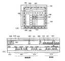
図21において、1001は実施例1の工程に従って作製したアクティブマトリクス基板であり、画素部1002、ゲート側駆動回路1003、ソース側駆動回路1004、信号分割回路1005、外部接続端子(I/Oポート)1006が形成されている。
【0210】
ここで図示しない対向基板は、シール材(封止材ともいう。代表的にはエポキシ系樹脂材料が用いられる。)1007でアクティブマトリクス基板1001と貼り合わせられ、シール材1007で囲まれた領域内に液晶が封入される。シール材1007にはフィラーと呼ばれる球状または棒状の固いスペーサ(無機材料からなるスペーサ)が予め添加されており、シール材をアクティブマトリクス基板にスクリーン印刷する際に同時に配置される。
【0211】
本実施例では、このシール材1007が形成される位置に対してフォトリソグラフィによりスペーサ(第1スペーサ)1008が形成される。また、画素部1002、ゲート側駆動回路1003、ソース側駆動回路1004または信号分割回路1005など各領域間の隙間に、フォトリソグラフィによりスペーサ1009(第2スペーサ)が形成される。さらに、画素部内には図12(B)や図19に示した位置にフォトリソグラフィによりスペーサ(第3スペーサ)1010が形成される。
【0212】
また、1011で示される領域を拡大して模式的に表したのが図21(B)である。基板1012上には、シフトレジスタ回路等を形成するCMOS回路1013、サンプリング回路1014及び画素部に形成される画素TFT1015が形成され、層間絶縁膜1016を介して保持容量1017と画素電極1018が形成されている。
【0213】
また、1019は対向基板、1020は対向電極であり、対向基板とアクティブマトリクス基板との間にはスペーサを介して液晶1021が封入される。このとき、シール材1007の中には、樹脂材料からなるスペーサ(第1スペーサ)1008と無機材料からなるスペーサ(フィラー)1022が含まれている。
【0214】
そして、CMOS回路1013やサンプリング回路1014等で形成される駆動回路と画素部との隙間に樹脂材料からなるスペーサ(第2スペーサ)1009が形成されている。また、駆動回路の内部においても、例えばシフトレジスタ回路とサンプリング回路の間のように、回路間又は素子間の隙間に樹脂材料からなるスペーサ(第4スペーサ)1023を設けることができる。
【0215】
また、図21(B)では画素TFT1015と画素電極1018とのコンタクト部の上に樹脂材料からなるスペーサ(第3スペーサ)1010が形成されている。なお、併用して保持容量1017の上にも樹脂材料からなるスペーサを設けることは可能である。また、コンタクト部には設けずに、保持容量1017の上にだけ樹脂材料からなるスペーサを設けることも可能である。
【0216】
以上のように、樹脂材料からなるスペーサはフォトリソグラフィにて形成するため自由に配置を設計することが可能である。本実施例はその利点を用い、TFTが形成されない領域に選択的にスペーサを設けることを特徴とする。
【0217】
なお、図21(B)に図示されたスペーサ1008〜1010、1023はすべて同時に用いる必要はなく、単独または組み合わせて用いることができ、その組み合わせは自由である。
【0218】
例えば、対角1インチ以下のアクティブマトリクス型液晶表示装置においては、パネルサイズが十分に小さいので、シール材が形成される位置に第1スペーサ1008を設けるだけでも良い場合がある。勿論、第1スペーサ1008と第2スペーサ1009の組み合わせ、第1スペーサ1008と第4スペーサ1023との組み合わせ、若しくは第1スペーサ1008と第2スペーサ1009と第4スペーサ1023との組み合わせでも良い。
【0219】
また、シール材が形成される位置は無機材料からなるスペーサ1022だけにしておき、第2スペーサ1009と第3スペーサ1010の組み合わせ、若しくは第4スペーサ1023と第3スペーサ1010の組み合わせとしても良い。
【0220】
また、駆動回路付近にはスペーサを置かず、第1スペーサ1008と第3スペーサ1010の組み合わせとすることもできる。
【0221】
また、第1スペーサ1008と第3スペーサ1010と第4スペーサ1023の組み合わせ、若しくは第1スペーサ1008と第2スペーサ1009と第3スペーサ1010の組み合わせでも良い。
【0222】
また、本実施例では画素部の構造として図18で説明した構造を例にしているが、図2の構造としても良い。
【0223】
なお、本実施例の構成は、実施例1〜14のいずれの構成とも自由に組み合わせることが可能である。
【0224】
[実施例16]
本発明は半導体基板を用いた従来のMOSFET上に層間絶縁膜を形成し、その上にTFTを形成する際に用いることも可能である。即ち、三次元構造の半導体装置を実現することも可能である。
【0225】
また、反射型液晶表示装置を作製する場合に限り、基板としてSIMOX、Smart−Cut(SOITEC社の登録商標)、ELTRAN(キャノン株式会社の登録商標)などのSOI基板を用いることも可能である。勿論、これらのSOI技術を用いて透明基板上に単結晶半導体薄膜を形成する技術が確立されれば、透過型表示装置に用いることも可能となる。
【0226】
なお、本実施例の構成は、実施例1〜15のいずれの構成とも自由に組み合わせることが可能である。
【0227】
[実施例17]
本願発明はアクティブマトリクス型EL(エレクトロルミネッセンス)表示装置やアクティブマトリクス型EC(エレクトロクロミックス)表示装置に対して実施することも可能である。本実施例ではアクティブマトリクス型EL表示装置に実施した例を図22に示す。
【0228】
図22はアクティブマトリクス型EL表示装置の回路図である。81は画素部を表しており、その周辺にはX方向(ソース側)駆動回路82、Y方向(ゲート側)駆動回路83が設けられている。また、画素部81の各画素は、スイッチ用TFT84、コンデンサ85、電流制御用TFT86、有機EL素子87を有し、スイッチ用TFT84にX方向(ソース側)信号線88a(または88b)、Y方向(ゲート側)信号線89a(または89b、89c)が接続される。また、電流制御用TFT86には、電源線90a、90bが接続される。
【0229】
本実施例のアクティブマトリクス型EL表示装置では、X方向駆動回路82、Y方向駆動回路83を図8(C)のpチャネル型TFT701、nチャネル型TFT702または703を組み合わせて形成する。また、スイッチ用TFT84を図8(B)のnチャネル型TFT704で形成し、電流制御用TFT86を図8(C)のpチャネル型TFT701で形成する。また、コンデンサ85として本発明により図8(A)の保持容量572を用いて形成する。
【0230】
ところで、TFTの上方に向かって(TFTを形成した基板を通さずに)光出射を行う動作モードのEL表示装置の場合、画素電極を反射性の電極で形成することになる。EL表示装置において画素内のどこにEL素子を配置するかは画素構造によっても異なるが、このような動作モードの場合、画素電極の上は全て有効表示領域として用いることができるため、保持容量の上にもEL素子を形成することができる。
【0231】
その場合、遮蔽膜(但しこの場合電界遮蔽の効果しかない)に起因する段差があるとEL素子も段差を有するようになり、その部分で発光方向が乱れるので画像表示の明るさや色合いを低下させる原因にもなる。本発明はこのような状況を解決する手段としても有効である。
【0232】
なお、本実施例のアクティブマトリクス型EL表示装置のコンデンサ85に対して樹脂材料からなる充填物によるピンホールの埋め込みを行うことは有効である。本実施例は、実施例5〜11、実施例12(特に図16または図17の作製工程)、実施例14、実施例16のいずれの構成とも自由に組み合わせることが可能である。
【0233】
[実施例18]
本願発明によって作製された液晶表示装置は様々な液晶材料を用いることが可能である。そのような材料として、TN液晶、PDLC(ポリマー分散型液晶)、スメクチック液晶が挙げられる。スメクチック液晶としては代表的にFLC(強誘電性液晶)、AFLC(反強誘性電液晶)、またはFLCとAFLCの混合物(反強誘電性混合液晶)が挙げられる。
【0234】
例えば、「H.Furue et al.;Charakteristics and Drivng Scheme of Polymer-Stabilized Monostable FLCD Exhibiting Fast Response Time and High Contrast Ratio with Gray-Scale Capability,SID,1998」、「T.Yoshida et al.;A Full-Color Thresholdless Antiferroelectric LCD Exhibiting Wide Viewing Angle with Fast Response Time,841,SID97DIGEST,1997」、「S.Inui et al.;Thresholdless antiferroelectricity in liquid crystals and its application to displays,671-673,J.Mater.Chem.6(4),1996」、または米国特許第5,594,569号に開示された材料を用いることができる。
【0235】
特に、電場に対して透過率が連続的に変化する電気光学応答特性を示す無しきい値反強誘電性混合液晶(Thresholdless Antiferroelectric LCD:TL−AFLCと略記する)にはV字型(またはU字型)の電気光学応答特性を示すものがあり、その駆動電圧が約±2.5V程度(セル厚約1μm〜2μm)のものも見出されている。ここで、V字型の電気光学応答を示す無しきい値反強誘電性混合液晶の印加電圧に対する光透過率の特性を示す例を図23に示す。
【0236】
図23に示すグラフの縦軸は透過率(任意単位)、横軸は印加電圧である。なお、液晶表示装置の入射側の偏光板の透過軸は、液晶表示装置のラビング方向にほぼ一致する無しきい値反強誘電性混合液晶のスメクティック層の法線方向とほぼ平行に設定されている。また、出射側の偏光板の透過軸は、入射側の偏光板の透過軸に対してほぼ直角(クロスニコル)に設定されている。
【0237】
図23に示されるように、このような無しきい値反強誘電性混合液晶を用いると、低電圧駆動かつ階調表示が可能となることがわかる。
【0238】
そのため、画素部用の電源電圧が5〜8V程度で済む場合があり、駆動回路と画素部を同じ電源電圧で動作させる可能性が示唆されている。即ち、液晶表示装置全体の低消費電力化を図ることができる。
【0239】
また、強誘電性液晶や反強誘電性液晶はTN液晶に比べて応答速度が速いという利点をもつ。本発明で用いるようなTFTは非常に動作速度の速いTFTを実現しうるため、強誘電性液晶や反強誘電性液晶の応答速度の速さを十分に生かした画像応答速度の速い液晶表示装置を実現することが可能である。
【0240】
また、一般に、無しきい値反強誘電性混合液晶は自発分極が大きく、液晶自体の誘電率が高い。このため、無しきい値反強誘電性混合液晶を液晶表示装置に用いる場合には、画素に比較的大きな保持容量が必要となってくる。よって、自発分極が小さな無しきい値反強誘電性混合液晶を用いるのが好ましい。そういった意味で本願発明の保持容量は小さい面積で大きな容量を蓄積することができるので好ましい。
【0241】
なお、本実施例の液晶表示装置をパーソナルコンピュータ等の表示ディスプレイとして用いることが有効であることは言うまでもない。
【0242】
また、本実施例の構成は、実施例1〜16のいずれの構成とも自由に組み合わせることが可能である。
【0243】
[実施例19]
本発明の電気光学装置は電気器具(電子装置もしくは電子デバイスともいう)の表示部として用いることができる。そのような電気器具としては、ビデオカメラ、デジタルカメラ、プロジェクター、プロジェクションTV、ゴーグル型ディスプレイ(ヘッドマウントディスプレイ)、ナビゲーションシステム、音響再生装置、ノート型パーソナルコンピュータ、ゲーム機器、携帯情報端末(モバイルコンピュータ、携帯電話、携帯型ゲーム機または電子書籍等)、記録媒体を備えた画像再生装置などが挙げられる。それら電気器具の具体例を図24〜26に示す。
【0244】
図24(A)は携帯電話であり、本体2001、音声出力部2002、音声入力部2003、表示部2004、操作スイッチ2005、アンテナ2006で構成される。本発明の電気光学装置は表示部2004に用いることができる。
【0245】
図24(B)はビデオカメラであり、本体2101、表示部2102、音声入力部2103、操作スイッチ2104、バッテリー2105、受像部2106で構成される。本発明の電気光学装置は表示部2102に用いることができる。
【0246】
図24(C)はモバイルコンピュータ(モービルコンピュータ)であり、本体2201、カメラ部2202、受像部2203、操作スイッチ2204、表示部2205で構成される。本発明の電気光学装置は表示部2205に用いることができる。
【0247】
図24(D)はゴーグル型ディスプレイであり、本体2301、表示部2302、アーム部2303で構成される。本発明の電気光学装置は表示部2302に用いることができる。
【0248】
図24(E)はリアプロジェクター(プロジェクションTV)であり、本体2401、光源2402、液晶表示装置2403、偏光ビームスプリッタ2404、リフレクター2405、2406、スクリーン2407で構成される。本発明は液晶表示装置2403に用いることができる。
【0249】
図24(F)はフロントプロジェクターであり、本体2501、光源2502、液晶表示装置2503、光学系2504、スクリーン2505で構成される。本発明は液晶表示装置2503に用いることができる。
【0250】
図25(A)はパーソナルコンピュータであり、本体2601、映像入力部2602、表示部2603、キーボード2604等を含む。本発明の電気光学装置は表示部2603に用いることができる。
【0251】
図25(B)は電子遊戯機器(ゲーム機器)であり、本体2701、記録媒体2702、表示部2703及びコントローラー2704を含む。この電子遊技機器から出力された音声や映像は筐体2705及び表示部2706を含む表示ディスプレイにて再生される。コントローラー2704と本体2701との間の通信手段または電子遊技機器と表示ディスプレイとの間の通信手段は、有線通信、無線通信もしくは光通信が使える。本実施例では赤外線をセンサ部2707、2708で検知する構成となっている。本発明の電気光学装置は表示部2703、2706に用いることができる。
【0252】
図25(C)はプログラムを記録した記録媒体(以下、記録媒体と呼ぶ)を用いるプレーヤー(画像再生装置)であり、本体2801、表示部2802、スピーカ部2803、記録媒体2804及び操作スイッチ2805を含む。なお、この画像再生装置は記録媒体としてDVD(Digital VersatileDisc)、CD等を用い、音楽鑑賞や映画鑑賞やゲームやインターネットを行うことができる。本発明の電気光学装置は表示部2802に用いることができる。
【0253】
図25(D)はデジタルカメラであり、本体2901、表示部2902、接眼部2903、操作スイッチ2904、受像部(図示せず)を含む。本発明の電気光学装置は表示部2902に用いることができる。
【0254】
なお、図24(E)のリアプロジェクターや図24(F)のフロントプロジェクターに用いることのできる光学エンジンについての詳細な説明を図26に示す。なお、図26(A)は光学エンジンであり、図26(B)は光学エンジンに内蔵される光源光学系である。
【0255】
図26(A)に示す光学エンジンは、光源光学系3001、ミラー3002、3005〜3007、ダイクロイックミラー3003、3004、光学レンズ3008a〜3008c、プリズム3011、液晶表示装置3010、投射光学系3012を含む。投射光学系3012は、投射レンズを備えた光学系である。本実施例は液晶表示装置3010を三つ使用する三板式の例を示したが、単板式であってもよい。また、図26(A)中において矢印で示した光路には、光学レンズ、偏光機能を有するフィルム、位相差を調節するためのフィルムもしくはIRフィルム等を設けてもよい。
【0256】
また、図26(B)に示すように、光源光学系3001は、光源3013、3014、合成プリズム3015、コリメータレンズ3016、3020、レンズアレイ3017、3018、偏光変換素子3019を含む。なお、図26(B)に示した光源光学系は光源を2つ用いたが、一つでも良いし、三つ以上としてもよい。また、光源光学系の光路のどこかに、光学レンズ、偏光機能を有するフィルム、位相差を調節するフィルムもしくはIRフィルム等を設けてもよい。
【0257】
以上の様に、本発明の適用範囲は極めて広く、あらゆる分野の電気器具に適用することが可能である。また、本実施例の電気器具は実施例1〜18の構成を必要に応じて組み合わせることで実現できる。
【発明の効果】
本願発明を用いることで、1)保持容量の誘電体のピンホールを塞ぐことができる、2)配向膜の平坦度(画素電極の平坦度)が向上する、といった利点が得られる。即ち、1)により保持容量における電極間のショートを防ぐことができ、2)により液晶の配向不良を防ぐことができる。
【0258】
また、弾力性に富む樹脂材料からなるスペーサを用いることで、素子にかかる負荷を低減し、素子破壊等による歩留まりの低下、信頼性の低下を防ぐことが可能となる。このように液晶表示装置に代表される電気光学装置の動作性能の向上と信頼性の向上とを達成することができる。
【0259】
また、延いてはそのような電気光学装置を表示ディスプレイとして有する電気器具の動作性能と信頼性をも向上させることができる。
【図面の簡単な説明】
【図1】 コンデンサの構造を示す図。
【図2】 液晶表示装置の画素構造を示す図。
【図3】 改善前のコンデンサの構造を示す図。
【図4】 改善前の液晶表示装置の画素構造を示す図。
【図5】 画素部と駆動回路の作製工程を示す図。
【図6】 画素部と駆動回路の作製工程を示す図。
【図7】 画素部と駆動回路の作製工程を示す図。
【図8】 画素部と駆動回路の作製工程を示す図。
【図9】 nチャネル型TFTのLDD構造を示す図。
【図10】 アクティブマトリクス型液晶表示装置の斜視図。
【図11】 アクティブマトリクス型液晶表示装置の回路ブロック図。
【図12】 画素の構造を示す上面図。
【図13】 アクティブマトリクス型液晶表示装置の断面図。
【図14】 画素部及び電源線と遮蔽膜の接続構造を示す断面図。
【図15】 液晶表示装置の画素構造を示す図。
【図16】 液晶表示装置の画素構造の作製工程を示す図。
【図17】 液晶表示装置の画素構造の作製工程を示す図。
【図18】 液晶表示装置の画素構造を示す図。
【図19】 画素の構造を示す上面図。
【図20】 液晶表示装置の画素構造を示す図。
【図21】 スペーサの形成位置を示す図。
【図22】 アクティブマトリクス型EL表示装置の構成を示す図。
【図23】 無しきい値反強誘電性混合液晶の光透過率特性を示す図。
【図24】 電気器具の一例を示す図。
【図25】 電気器具の一例を示す図。
【図26】 光学エンジンの構成を示す図。
【符号の説明】
501 基板
502 下地膜
503 結晶質シリコン膜
504 結晶質シリコン膜
505〜508 活性層
509 保護膜
511〜513 p型不純物領域(b)が形成された活性層
515〜517 n型不純物領域(b)
518 ゲート絶縁膜
519 第1導電膜
520 第2導電膜
521〜524 ゲート配線
525〜530 n型不純物領域(c)
531〜534 ゲート絶縁膜
536〜544 n型不純物領域(a)
546、547 p型不純物領域(a)
548 第1層間絶縁膜
549〜553 チャネル形成領域
554 第2層間絶縁膜
555〜558 ソース配線
559〜562 ドレイン配線
563 パッシベーション膜
564 第3層間絶縁膜
565 遮蔽膜
566 酸化シリコン膜
567 酸化物
568 樹脂材料からなるスペーサ
569〜571 画素電極
572 保持容量
573、576 配向膜
574 対向基板
575 対向電極
578 液晶
601、604、608、613、614 チャネル形成領域
602、605、609、615 ソース領域
603、606、610、616 ドレイン領域
607、611a、612a Lov領域
611b、612b、617〜620 Loff領域
621 n型不純物領域(a)[0001]
BACKGROUND OF THE INVENTION
The present invention relates to a semiconductor device having a circuit formed of a thin film transistor (hereinafter referred to as TFT) on an insulator (substrate) having an insulating surface and a manufacturing method thereof. In particular, the present invention relates to an electro-optical device typified by a liquid crystal display device in which a pixel portion and a drive circuit provided in the periphery thereof are provided on the same insulator, and an electric appliance (electronic device) equipped with the electro-optical device. Note that in this specification, a semiconductor device refers to all devices that function by utilizing semiconductor characteristics, and the semiconductor device includes the electro-optical device and an electric appliance in which the electro-optical device is mounted.
[0002]
[Prior art]
Development of a semiconductor device having a large-area integrated circuit formed using a TFT over a substrate having an insulating surface is in progress. Liquid crystal display devices, EL (electroluminescence) display devices, and contact image sensors are known as representative examples. In particular, a TFT having a polysilicon film (polycrystalline silicon film) as an active layer (hereinafter referred to as a polysilicon TFT) has a high field effect mobility and can be used for circuits having various functions.
[0003]
For example, in an active matrix liquid crystal display device, a pixel portion that performs image display and a drive circuit including a shift register, a level shifter, a buffer, a sampling circuit, and the like based on a CMOS circuit are formed over the same substrate. In the contact image sensor, a driving circuit for controlling a pixel portion such as a sample hold circuit, a shift register, and a multiplexer is formed using TFTs.
[0004]
Further, in the pixel portion of the active matrix liquid crystal display device, a TFT (hereinafter referred to as a pixel TFT) is arranged for each of tens to millions of pixels, and a pixel electrode is provided for each of the pixel TFTs. Yes. A counter electrode is provided on the counter substrate side with the liquid crystal interposed therebetween, and a kind of capacitor using the liquid crystal as a dielectric is formed. Then, the voltage applied to each pixel is controlled by the switching function of the pixel TFT, and the liquid crystal is driven by controlling the charge to this capacitor, and the transmitted light quantity is controlled to display an image.
[0005]
However, the storage capacity of this capacitor gradually decreases due to the leakage current caused by the off current of the pixel TFT (drain current that flows even though the TFT is in the off state as a switch), and thus the amount of transmitted light changes. As a result, the image display contrast is reduced. Therefore, conventionally, a capacitor (holding capacity) different from the capacitor using liquid crystal as a dielectric is provided in parallel to compensate for the loss of the capacitor using liquid crystal as a dielectric.
[0006]
[Problems to be solved by the invention]
As examples of the storage capacitor provided in the pixel portion of the electro-optical device, the applicant has already filed Japanese Patent Application Nos. 11-045558, 11-053424, and 11-059455. These applications disclose an invention in which a storage capacitor is formed by a shielding film (or a light shielding film), an oxide formed on the surface of the shielding film, and a pixel electrode.
[0007]
However, there is a concern that the following problems may occur in the storage capacities disclosed in those applications. This will be described.
[0008]
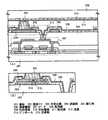
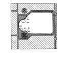
In FIG. 3,
[0009]
If the
[0010]
In FIG. 4,
[0011]
At this time, if the flatness of the
[0012]
As described above, the problems described with reference to FIGS. 3 and 4 do not necessarily occur, but may cause a decrease in yield. It is an object of the present invention to provide means for solving the above problems.
[0013]
That is, it is an object of the present invention to further improve the invention relating to the storage capacitor described in the above application specification, and to improve the operation performance and reliability of the semiconductor device. Another object is to provide a manufacturing method for realizing such a semiconductor device.
[0014]
[Means for Solving the Problems]
As a means for solving the above problems, in the present invention, in forming the storage capacitor described in the above-mentioned application specification, the anodic oxide formed on the surface of the conductive film to be the lower electrode of the storage capacitor is temporarily insulated. The pinhole formed in the anodic oxide is covered with and filled with the insulator.
[0015]
This is shown in FIG. In FIG. 1, on a base
[0016]
As the
[0017]
When an insulating film made of a resin material is used, a photopolymerization type insulating film or a heat polymerization type insulating film may be used. Moreover, although it may have negative photosensitivity or positive photosensitivity, it is desirable to use a resin material having negative photosensitivity in order to avoid photodegradation.
[0018]
In addition, the short circuit of the holding capacity due to the spacer pressure described in FIG. 4 can be avoided by using a spacer made of a resin material. Since the spacer made of resin material is rich in elasticity, it absorbs pressure appropriately, and unlike the bead-shaped spacer, it contacts the element on the surface, so the pressure is dispersed and there is no excess pressure applied to one point. Because.
[0019]
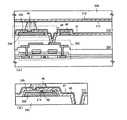
In FIG. 2A, a
[0020]
Further, a
[0021]
The feature of FIG. 2 (A) is not only using a spacer made of a resin material but also positively using a resin material applied when forming the spacer for filling hole holes in the
[0022]
Here, an enlarged view of a region surrounded by a dotted
[0023]
As described above, in the present invention, in order to prevent a short-circuit due to a pinhole that is unintentionally formed in the dielectric of the storage capacitor, first, defects caused by the formation of the storage capacitor are buried by filling the pinhole with an insulator. prevent. Furthermore, by forming the spacer with an insulating film made of a resin material, the element is prevented from being destroyed by the pressure applied from the spacer on the storage capacitor.
[0024]
Furthermore, in the present invention, it is also possible to achieve the filling of the pinhole formed in the dielectric of the storage capacitor simultaneously with the formation of the spacer made of the resin material. That is, it is possible to eliminate defects related to the storage capacitor without increasing the number of special steps and to improve the yield in the manufacturing process.
[0025]
DETAILED DESCRIPTION OF THE INVENTION
The embodiment of the present invention will be described in detail with reference to the following examples.
[0026]
[Example 1]
An embodiment of the present invention will be described with reference to FIGS. Here, a method for simultaneously manufacturing a pixel portion and a driver circuit provided around the pixel portion will be described. However, in order to simplify the description, regarding the driving circuit, a CMOS circuit which is a basic circuit such as a shift register and a buffer, and an n-channel TFT forming a sampling circuit (transfer gate) are illustrated.
[0027]
In FIG. 5A, a glass substrate or a quartz substrate is preferably used for the
[0028]
A base film made of an insulating film containing silicon (referred to generically as a silicon oxide film, a silicon nitride film, or a silicon nitride oxide film in this specification) is formed on the surface of the
[0029]
Note that in this specification, a silicon nitride oxide film is an insulating film expressed by SiOxNy and indicates an insulating film containing silicon, oxygen, and nitrogen at a predetermined ratio. In this embodiment, as the
[0030]
Note that the
[0031]
Next, a semiconductor film including an amorphous structure (in this embodiment, an amorphous silicon film (not shown)) having a thickness of 30 to 120 nm (preferably 50 to 70 nm) is formed on the
[0032]
Then, a semiconductor film (crystalline silicon film in this embodiment) 503 including a crystal structure is formed according to a technique described in Japanese Patent Laid-Open No. 7-130552 (corresponding to USP 5,643,826). The technology described in the publication is a catalyst element (one or more elements selected from nickel, cobalt, germanium, tin, lead, palladium, iron, and copper) that promotes crystallization when crystallizing an amorphous silicon film. , Typically nickel).
[0033]
Specifically, heat treatment is performed with the catalytic element held on the surface of the amorphous silicon film to change the amorphous silicon film into a crystalline silicon film. In this embodiment, the technique described in the first embodiment of the publication is used, but the technique described in the second embodiment may be used. The crystalline silicon film includes a so-called single crystal silicon film and a polycrystalline silicon film, but the crystalline silicon film formed in this embodiment is a silicon film having a crystal grain boundary. (Fig. 5 (A))
[0034]
Although it depends on the amount of hydrogen contained in the amorphous silicon film, it is preferable that the dehydrogenation treatment is performed by heating at 400 to 550 ° C. for several hours, and the crystallization step is performed with the amount of hydrogen contained being 5 atom% or less. . Although an amorphous silicon film may be formed by other manufacturing methods such as a sputtering method or an evaporation method, it is desirable to sufficiently reduce impurity elements such as oxygen and nitrogen contained in the film.
[0035]
Here, since the base film and the amorphous silicon film can be formed by the same film formation method, they may be formed continuously. After the formation of the base film, it is possible to prevent surface contamination by preventing exposure to the air atmosphere and to reduce variation in characteristics of the manufactured TFT.
[0036]
Next, the
[0037]
Further, instead of laser light, light emitted from a lamp (hereinafter referred to as lamp light) may be irradiated (hereinafter referred to as lamp annealing). As the lamp light, lamp light emitted from a halogen lamp, an infrared lamp, or the like can be used.
[0038]
In addition, the process of performing heat treatment (annealing) with laser light or lamp light in this way is called a light annealing process. Since the light annealing process can be performed at a high temperature in a short time, an effective heat treatment process can be performed with high throughput even when a substrate having low heat resistance such as a glass substrate is used. Of course, since the purpose is annealing, furnace annealing (also referred to as thermal annealing) using an electric furnace can be used instead.
[0039]
In this embodiment, the laser annealing process is performed by processing pulsed excimer laser light into a linear shape. The laser annealing conditions are as follows: XeCl gas is used as the excitation gas, the processing temperature is room temperature, the pulse oscillation frequency is 30 Hz, and the laser energy density is 250 to 500 mJ / cm.2(Typically 350-400mJ / cm2).
[0040]
The laser annealing step performed under the above conditions has the effect of completely crystallizing the amorphous region remaining after thermal crystallization and reducing defects in the already crystallized crystalline region. Therefore, this step can also be called a step of improving the crystallinity of the semiconductor film by light annealing or a step of promoting the crystallization of the semiconductor film. Such an effect can also be obtained by optimizing the lamp annealing conditions. In this specification, such a condition is referred to as first optical annealing.
[0041]
Next, the
[0042]
Next, a
[0043]
Then, a resist
[0044]
Thus 1 × 10¹⁵~ 1x10¹⁸atoms / cmThree(Typically 5 × 10¹⁶~ 5x10¹⁷atoms / cmThree)
[0045]
Note that in this specification, an impurity region containing a p-type impurity element in the above concentration range (however, 1 × 10 1016atoms / cmThreeAn impurity element that imparts n-type at a concentration of typically, except for a region to which phosphorus or arsenic is added) is defined as a p-type impurity region (b). (Fig. 5 (D))
[0046]
Next, the resist
[0047]
These low-
[0048]
Here, phosphine (PHThree) By mass-separated plasma-excited ion doping method with 1 × 10 phosphorus18atoms / cmThreeAdd at a concentration of Of course, an ion implantation method for performing mass separation may be used. In this step, phosphorus is added to the crystalline silicon film through the
[0049]
Next, the resist
[0050]
In this embodiment, the laser annealing process is performed by processing pulsed excimer laser light into a linear shape. The laser annealing conditions are as follows: KrF gas is used as the excitation gas, the processing temperature is room temperature, the pulse oscillation frequency is 30 Hz, and the laser energy density is 100 to 300 mJ / cm.2(Typically 150-250mJ / cm2).
[0051]
The optical annealing step performed under the above conditions has an effect of activating the added n-type or p-type impurity element and recrystallizing the amorphous semiconductor film when the impurity element is added. . Note that it is preferable that the above conditions ensure atomic arrangement consistency without melting the semiconductor film and activate the impurity element. This step can also be called a step of activating an impurity element imparting n-type or p-type by light annealing, a step of recrystallizing a semiconductor film, or a step of simultaneously performing them. Such an effect can also be obtained by optimizing the lamp annealing conditions. In this specification, such a condition is referred to as second optical annealing. Note that the second light annealing can be omitted.
[0052]
By this step, an intrinsic region existing in the boundary portion of the n-type impurity region (b) 515 to 517, that is, around the n-type impurity region (b) (the p-type impurity region (b) is also regarded as substantially intrinsic). And the joint part becomes clear. This means that when the TFT is later completed, the LDD region and the channel formation region can form a very good junction.
[0053]
When the impurity element is activated by the laser beam, activation by heat treatment (furnace annealing) using an electric furnace may be used in combination, or activation may be performed only by furnace annealing. When activation by heat treatment is performed, heat treatment at 450 to 650 ° C. (preferably 500 to 550 ° C.) may be performed in consideration of heat resistance of the substrate.
[0054]
Next, a
[0055]
Next, a conductive film to be a gate wiring is formed. Note that although the gate wiring may be formed using a single-layer conductive film, it is preferable to form a stacked film such as two layers or three layers as necessary. In this embodiment, a stacked film including a first
[0056]
Here, as the first
[0057]
Note that the first
[0058]
In addition, a laminated film of a tungsten nitride film and a tungsten film, a single-layer film including only a tantalum nitride film, and a tungsten silicide film are also suitable. In addition, when a silicon film is formed under the first
[0059]
Further, when a metal film is used as the second
[0060]
Next, the first
[0061]
Next, an n-type impurity element (phosphorus in this embodiment) is added in a self-aligning manner using the gate wirings 521 to 524 as a mask.
[0062]
Note that the n-type impurity regions (c) 527 to 530 are already 1 × 10 5 in the channel doping process.15~ 1x10¹⁸atoms / cmThreeIn this step, since phosphorus is added at a
[0063]
However, strictly speaking, the phosphorus concentration of the portion of the n-type impurity region (b) 515 to 517 overlapping the gate wiring is 2 × 10¹⁶~ 5x10¹⁹atoms / cmThreeWhereas the portion that does not overlap the gate wiring is 1 × 10¹⁶~ 5x10¹⁸atoms / cmThreeThe concentration of phosphorus is added, and phosphorus is contained at a slightly higher concentration.
[0064]
Next, the
[0065]
By exposing the active layer in this manner, the acceleration voltage can be lowered when the impurity element is added next. As a result, the throughput is improved because the required dose is small. Of course, the impurity region may be formed by through doping while leaving the gate insulating film unetched.
[0066]
Next, resist
[0067]
In this specification, an impurity region containing an n-type impurity element in the above concentration range is defined as an n-type impurity region (a). The region where the
[0068]
Next, the resist
[0069]
Note that a part of the
[0070]
Next, after removing the resist
[0071]
In this example, SiH is used by plasma CVD.Four, N2O, NHThreeAs a source gas, a 200 nm thick silicon nitride oxide film (however, the nitrogen concentration is 25 to 50 atomic%) is used. The first
[0072]
Thereafter, a heat treatment step is performed to activate the n-type or p-type impurity element added at each concentration. This step can be performed by a furnace annealing method, a laser annealing method, or a rapid thermal annealing method (RTA method). Here, the activation process is performed by furnace annealing. In this heat treatment step, heat treatment is performed in a nitrogen atmosphere at 300 to 650 ° C., preferably 400 to 550 ° C., here 550 ° C. for 4 hours. (Fig. 7 (B))
[0073]
At this time, the catalyst element (nickel in this embodiment) used for crystallization of the amorphous silicon film in this embodiment moves in the direction indicated by the arrow, and is formed in the process of FIG. It is captured (gettered) in a region containing phosphorus at a high concentration. This is a phenomenon caused by the gettering effect of the metal element by phosphorus. As a result, the concentration of the catalyst element in the subsequent
[0074]
On the contrary, in the region serving as the gettering site of the catalytic element (the region where the
[0075]
Next, a process of hydrogenating the active layer is performed by performing a heat treatment at 300 to 450 ° C. for 1 to 12 hours in an atmosphere containing 3 to 100% hydrogen. This step is a step of terminating dangling bonds in the semiconductor layer with thermally excited hydrogen. As another means of hydrogenation, plasma hydrogenation (using hydrogen excited by plasma) may be performed.
[0076]
When the activation process is completed, a second
[0077]
Note that as the second
[0078]
Thereafter, contact holes reaching the source region or the drain region of each TFT are formed, and source wirings 555 to 558 and
[0079]
Next, the
[0080]
At this time, prior to film formation, H2, NHThreeIt is effective to perform plasma treatment using a gas containing isohydrogen and to perform heat treatment after film formation. Hydrogen excited by this pretreatment is supplied into the first and second interlayer insulating films. By performing the heat treatment in this state, the film quality of the
[0081]
Further, after the
[0082]
Note that an opening may be formed in the
[0083]
After that, as shown in FIG. 7D, a third interlayer insulating film (referred to as a planarizing film in this specification) made of an insulating film (hereinafter also referred to as a resin insulating film) made of a resin material (or an organic material) is used. 564 (sometimes called) is formed to a thickness of about 1-3 μm (typically 1.5-2 μm).
[0084]
As the resin material, polyimide, acrylic resin, polyamide, polyimide amide, BCB (benzocyclobutene) or cycloten can be used. Advantages of using the resin insulating film include extremely excellent flatness and a low relative dielectric constant. A resin insulating film other than those described above, an organic SiO compound, or the like can also be used. In addition, an insulating film made of an inorganic material can be used as long as the flatness is high.
[0085]
Here, an acrylic film that is polymerized by heat after being applied to the substrate is used, but a type that is polymerized by light irradiation may be used. Of course, a positive or negative photosensitive material may be used.
[0086]
Further, as a part of the third
[0087]
Next, a
[0088]
Any metal film can be used as the
[0089]
In this embodiment, the silicon oxide film is formed to a thickness of 5 to 50 nm (typically 20 to 30 nm) before the
[0090]
The
[0091]
Further, it is possible to form not only the shielding film but also other connection wirings by using the aluminum film containing titanium. For example, it is possible to form a connection wiring that connects circuits in the drive circuit. However, in that case, it is necessary to form a contact hole in the third interlayer insulating film in advance before forming the material for forming the shielding film or the connection wiring.
[0092]
Next, an oxide having a thickness of 20 to 100 nm (preferably 30 to 50 nm) is formed on the surface of the
[0093]
Here, an insulator is provided only on the surface of the shielding film by using an anodic oxidation method, but another insulator (insulating film) is formed by a vapor phase method such as a plasma CVD method, a thermal CVD method, or a sputtering method. You may do it. Also in that case, the film thickness is preferably 20 to 100 nm (preferably 30 to 50 nm).
[0094]
Next, as shown in FIG. 8A, a 4 μm-thick resin insulation film (in this embodiment, a negative acrylic resin film) is formed, and
[0095]
The
[0096]
Next, a contact hole reaching the
[0097]
In the case of a reflective liquid crystal display device, a metal film such as an aluminum film or a silver thin film may be used as a material for the pixel electrode.
[0098]
At this time, the
[0099]
In this case, the shielding
[0100]
Thus, a substrate (hereinafter referred to as an active matrix substrate) having a driving circuit and a pixel portion on the same substrate is completed. Note that in FIG. 8B, a p-channel TFT 701 and n-
[0101]
In addition, you may change the process order of a present Example suitably. In any order, if the structure of the finally formed TFT is as shown in FIG. 8B, the basic function of the active matrix substrate does not change, and the effect of the present invention is not impaired. Absent.
[0102]
A
[0103]
In addition, a
[0104]
In the n-
[0105]
Here, the cross-sectional view shown in FIG. 9 is an enlarged view showing a state in which the n-
[0106]
In the
[0107]
According to this embodiment, the structure of the TFT for forming a circuit or an element can be optimized according to the performance required by the pixel portion and the drive circuit, and the operation performance and reliability of the semiconductor device can be improved. Specifically, n-channel TFTs have a low LDD region arrangement according to circuit specifications and use different Lov regions or Loff regions. A TFT structure with an emphasis on off-current operation can be realized.
[0108]
For example, in the case of an active matrix liquid crystal display device, the n-channel TFT 702 is suitable for a drive circuit such as a shift register, a signal dividing circuit, a level shifter, or a buffer that places importance on high-speed operation. That is, by disposing the Lov region only on one side (drain region side) of the channel formation region, it is possible to achieve an operation that is resistant to deterioration due to hot carrier injection while reducing the resistance component as much as possible. This is because in the case of the above circuit, the functions of the source region and the drain region are not changed, and the direction in which carriers (electrons) move is constant. However, Lov regions can be arranged on both sides of the channel formation region as necessary.
[0109]
The n-
[0110]
Further, the n-
[0111]
The length (width) of the
[0112]
Further, in this embodiment, an alumina film having a high relative dielectric constant of 7 to 9 is used as the dielectric of the storage capacitor, thereby making it possible to reduce the area for forming the necessary capacitance. Furthermore, by using the shielding film formed on the pixel TFT as one electrode of the storage capacitor as in this embodiment, the aperture ratio of the image display portion of the active matrix liquid crystal display device can be improved.
[0113]
Next, a process for manufacturing an active matrix liquid crystal display device from an active matrix substrate will be described. First, an
[0114]
Next, after forming an alignment film, a rubbing process is performed to adjust the liquid crystal molecules so that they are aligned with a certain pretilt angle. Then, the pixel portion, the active matrix substrate on which the driving circuit is formed, and the counter substrate are bonded together using a sealing material by a known cell assembling process.
[0115]
Thereafter,
[0116]
By implementing the invention of the present application, it becomes possible to block the pinhole that has been accidentally formed in the dielectric of the storage capacitor with an insulator, and solve the problem of short circuit between the shielding film and the pixel electrode. can do. That is, the yield of the manufacturing process can be greatly improved.
[0117]
In addition, when a resin material is used as in this embodiment in filling a pinhole, it is difficult to detect the pinhole itself, but there is more resin material in the position where the pinhole was present than in other regions. Will do. This means that a region having a high carbon concentration exists in the dielectric of the storage capacitor. In order to examine the distribution of the carbon concentration in the dielectric, known analysis means such as SIMS analysis (mass secondary ion analysis) and EDX (energy dispersive X-ray detector) may be used.
[0118]
Further, in this embodiment, since the spacer made of a resin material rich in elasticity is used, the pressure applied to the holding capacity can be absorbed (relaxed) in the pressing step described with reference to FIG. Further, since the spacer of this embodiment has a larger contact area with the element than that of the bead-shaped spacer, no excessive pressure is applied to a specific portion.
[0119]
In addition, since the formation position can be designed freely, the image display area can be used effectively. In the case of the present invention, it may be formed in a region not used as an image display region, such as on a shielding film or a source wiring. Of course, the spacer may be formed of an inorganic material as well as a resin material, and it is also effective to form a spacer in a tapered shape to widen the contact area with the alignment film (or pixel electrode) and to distribute the pressure. is there.
[0120]
[Example 2]
In this embodiment, the structure of the active matrix liquid crystal display device shown in Embodiment 1 will be described with reference to the perspective view of FIG. The active matrix substrate includes a
[0121]
Further, the drive circuit provided in the periphery is configured based on a CMOS circuit. The gate
[0122]
In this specification, the semiconductor device shown in FIG. 10 is called an active matrix liquid crystal display device, but a liquid crystal panel attached up to an FPC as shown in FIG. 10 is generally called a liquid crystal module. . Therefore, the active matrix liquid crystal display device in this embodiment may be called a liquid crystal module.
[0123]
[Example 3]
In this embodiment, an example of a circuit configuration of the liquid crystal display device shown in
[0124]
The source side driver circuit 901 includes a shift register 902, a level shifter 903, a buffer 904, and a sampling circuit 905. The gate side driver circuit (A) 907 includes a
[0125]
Here, the driving voltages of the shift registers 902 and 908 are 5 to 16 V (typically 10 V), and an n-channel TFT used in a CMOS circuit forming the circuit has a structure indicated by 702 in FIG. 8B. Is suitable.
[0126]
The
[0127]
Although the sampling circuit 905 has a driving voltage of 14 to 16 V, since the source region and the drain region are inverted and the off-current value needs to be reduced, the CMOS including the n-
[0128]
Further, since the pixel portion 906 requires a driving voltage of 14 to 16 V and a lower off-current value than the sampling circuit 905, it is desirable that the Lov region that causes an increase in off-current is not disposed. The n-
[0129]
Note that the structure of this embodiment can be easily realized by manufacturing a TFT in accordance with the manufacturing process shown in Embodiment 1. Further, in this embodiment, only the configuration of the pixel portion and the drive circuit is shown. However, according to the manufacturing process of Embodiment 1, in addition to the drive circuit such as a signal dividing circuit, a D / A converter, an operational amplifier, and a γ correction circuit. These logic circuits (signal processing circuits) can be formed on the same substrate, and further, a memory portion, a microprocessor, and the like can be formed.
[0130]
[Example 4]
In this embodiment, an embodiment relating to the structure of a plurality of pixels forming the pixel portion is shown. FIG. 12 is used for the description.
[0131]
First, in FIG. 12A, 11 is an active layer, 12 is a gate wiring (including a gate electrode), 13 is a source wiring, 14 is a drain wiring, and 15 and 16 are the
[0132]
Further, as shown in FIG. 12B, the shielding
[0133]
At this time, a region where the above-described
[0134]
As described above, by using the present invention, a storage capacitor that can secure a large capacitance with a small area can be formed. Further, the
[0135]
Note that the pixel structure is not limited to the structure of this embodiment. Further, the structure of this embodiment can be manufactured by the manufacturing process of Embodiment 1, and can be used as a pixel of the liquid crystal display device shown in
[0136]
[Example 5]
In this embodiment, an active matrix liquid crystal display having a pixel portion having a structure different from that in Embodiment 1 will be described with reference to FIG. Since the basic structure is the same as FIG. 8B, only the changes will be described. Therefore, the other portions are as described with reference to FIG.
[0137]
In the structure of FIG. 13, the structure of a pixel TFT (n-channel TFT) 705 that forms a pixel portion is different from that of the second embodiment. Specifically, in this embodiment, offset
[0138]
Note that the offset region is a semiconductor layer having the same composition as the channel formation region (meaning that the contained impurity element is the same as the channel formation region) as indicated by 32 to 35 and does not overlap with the gate electrode. . The offset
[0139]
In order to realize such a structure, for example, before adding an n-type impurity element in the step of FIG. 6D of Example 1, insulation including silicon with a thickness of 20 to 200 nm (preferably 25 to 150 nm) is performed. A film may be formed so as to cover the gate wiring or the like.
[0140]
By doing so, the impurity element is added in a state where the insulating films are formed on the side walls of the
[0141]
This insulating film is preferably the same as the material of the gate insulating film. Then, it can be removed at the same time as the gate insulating film in the step of FIG.
[0142]
In addition, the structure of a present Example is realizable by changing a part of process of Example 1, and can be combined freely with any structure of Examples 2-4.
[0143]
[Example 6]
The storage capacitor provided in each pixel of the pixel portion can be formed by setting the electrode (shielding film in the present invention) that is not connected to the pixel electrode to a fixed potential. In that case, it is desirable to set the shielding film to a floating state (electrically isolated state) or a common potential (an intermediate potential of an image signal sent as data).
[0144]
Therefore, in this embodiment, a connection method in the case where the shielding film is fixed to a common potential will be described with reference to FIG. Note that since the basic structure is the same as that of the pixel portion described in FIG. 8B, the same portions are described using the same reference numerals.
[0145]
In FIG. 14A,
[0146]
As described above, the shielding
[0147]
Next, in FIG. 14B,
[0148]
The
[0149]
In the case of employing the structure of FIG. 14B, it is preferable to employ source line inversion driving as a driving method of the active matrix liquid crystal display device. In the case of source line inversion driving, the voltage polarity applied to the pixel electrode is inverted every frame, so that the amount of charge accumulated in the
[0150]
By adopting the structure shown in FIG. 14B in this way, the shielding film can be held at a common potential without increasing the number of steps.
[0151]
Note that the configuration of this example can be realized by only partially changing the manufacturing process of Example 1, and the other processes may be similar to those of Example 1. Moreover, it is possible to combine freely with any structure shown in Examples 2-5.
[0152]
[Example 7]
In this example, an example of an anodic oxidation method in forming the
[0153]
In this example, first, an ethylene glycol tartrate solution having a sufficiently low alkali ion concentration is prepared. This is a solution of 15% ammonium tartrate aqueous solution and ethylene glycol mixed at 2: 8, and ammonia water is added to this to adjust the pH to 7 ± 0.5. Then, a platinum electrode serving as a cathode is provided in the solution, the substrate on which the
[0154]
The voltage between the cathode and the anode in the solution changes with time according to the growth of the anodic oxide, but the voltage is increased at a step-up rate of 100 V / min while maintaining a constant current. End the process. In this manner, an
[0155]
Even if the
[0156]
In addition, the present Example only changed the conditions of the anodizing process of Example 1, and can be freely combined with any structure of Examples 2-6.
[0157]
[Example 8]
In Example 1, after the step shown in FIG. 5B is finished, the
[0158]
In this case, the step of activating the p-type impurity region (b) and the n-type impurity region (b) (corresponding to the laser annealing step of FIG. 5F in Example 1) is performed by patterning the crystalline silicon film. You can do it before. Therefore, it is possible to prevent a problem that the optimum conditions for the laser annealing process change depending on the pattern design (position, shape, etc. of the active layer). That is, there is an advantage that the degree of freedom of design at the time of TFT formation is improved.
[0159]
In addition, the present Example only changed the process order of Example 1, and can be freely combined with any structure of Examples 2-7.
[0160]
[Example 9]
In the manufacturing process shown in Embodiment 1, an example is shown in which a channel doping process is performed only on a region to be an n-channel TFT to control the threshold voltage. However, an n-channel TFT or a p-channel TFT is used. It is also possible to perform a channel doping process on the entire surface without distinction. In that case, since the number of photomasks in the manufacturing process is reduced, the throughput and yield of the process can be improved.
[0161]
In some cases, the entire surface is subjected to a channel doping step, and an impurity element imparting a conductivity type opposite to that of the impurity element added to the entire surface is added to either the n-channel TFT or the p-channel TFT. It is possible.
[0162]
In addition, the structure of a present Example can be freely combined with any structure shown in Examples 1-8.
[0163]
[Example 10]
In the manufacturing process of Example 1, an example in which a catalytic element that promotes crystallization is used as a method for forming a semiconductor film including a crystal structure. However, in this example, thermal crystallization is performed without using such a catalytic element. A case where a semiconductor film including a crystal structure is formed by crystallization or laser crystallization is shown.
[0164]
In the case of thermal crystallization, a heat treatment step for 15 to 24 hours may be performed at a temperature of 600 to 650 ° C. after forming a semiconductor film including an amorphous structure. That is, by performing heat treatment at a temperature exceeding 600 ° C., natural nuclei are generated and crystallization proceeds.
[0165]
In the case of laser crystallization, a laser annealing process may be performed under the first annealing conditions described in Embodiment 1 after forming a semiconductor film including an amorphous structure. Thus, a semiconductor film including a crystal structure can be formed in a short time. Of course, lamp annealing may be performed instead of laser annealing.
[0166]
As described above, a semiconductor film including a crystal structure used for a TFT can be formed using any known means. In addition, a present Example can be freely combined with any structure of Examples 1-9.
[0167]
[Example 11]
In this example, the technique described in Example 1 of Japanese Patent Application No. 11-76967 is used as a method for producing a crystalline silicon film that becomes an active layer of a TFT. According to the manufacturing process of Example 1 of the same application specification, a crystalline silicon film having a unique crystal structure can be obtained.
[0168]
For details on the crystalline silicon film, refer to the applications of Japanese Patent Application No. 10-044659, Japanese Patent Application No. 10-152316, Japanese Patent Application No. 10-152308 or Japanese Patent Application No. 10-152305 filed by the present applicant. Just do it. Hereinafter, an outline of the characteristics of the crystal structure experimentally investigated by the applicant will be described. This feature may be considered to coincide with the feature of the semiconductor layer forming the active layer of the TFT completed by carrying out this embodiment.
[0169]
When viewed microscopically, the crystalline silicon film has a crystal structure in which a plurality of needle-like or rod-like crystals (hereinafter abbreviated as rod-like crystals) are gathered and arranged. This can be easily confirmed by observation with TEM (transmission electron microscopy).
[0170]
Further, when electron beam diffraction is used, the {110} plane can be confirmed as the orientation plane although the crystal silicon film surface (portion forming portion) includes a slight shift in the crystal axis. This is confirmed by observing diffraction spots having regularity specific to the {110} plane when an electron diffraction photograph having a spot diameter of about 1.35 μm is observed. It has also been confirmed that each spot has a concentric distribution.
[0171]
When the orientation ratio is calculated using an X-ray diffraction method (strictly, an X-ray diffraction method using the θ-2θ method), the orientation ratio of the {220} plane is 0.7 or more (typically 0.85 or more). In addition, the method described in Unexamined-Japanese-Patent No. 7-321339 is used for the calculation method of orientation ratio.
[0172]
Further, when a crystal grain boundary formed by contact of individual rod-like crystals is observed by HR-TEM (high resolution transmission electron microscopy), it can be confirmed that the crystal lattice has continuity at the crystal grain boundary. This can be easily confirmed because the observed lattice fringes are continuously connected at the grain boundaries.
[0173]
Note that the continuity of the crystal lattice at the crystal grain boundary results from the fact that the crystal grain boundary is a grain boundary called a “planar grain boundary”. The definition of the planar grain boundary in this specification is “Characterization of High-Efficiency Cast-Si Solar Cell Wafers by MBIC Measurement; Ryuichi Shimokawa and Yutaka Hayashi, Japanese Journal of Applied Physics vol.27, No.5, pp.751”. -758, 1988 ”is the“ Planar boundary ”.
[0174]
According to the above paper, planar grain boundaries include twin grain boundaries, special stacking faults, and special twist grain boundaries. This planar grain boundary is characterized by being electrically inactive. That is, although it is a crystal grain boundary, it does not function as a trap that inhibits the movement of carriers, and thus can be regarded as substantially absent.
[0175]
In particular, when the crystal axis (axis perpendicular to the crystal plane) is the <110> axis, the {211} twin grain boundary is also called a corresponding grain boundary of Σ3. The Σ value is a parameter that serves as a guideline indicating the degree of consistency of the corresponding grain boundary. It is known that the smaller the Σ value, the better the grain boundary. Actually, when the crystalline silicon film of this example is observed in detail using TEM, most of the crystal grain boundaries (90% or more, typically 95% or more) are the corresponding grain boundaries of Σ3, typically It turns out that it is a {211} twin grain boundary.
[0176]
In the crystal grain boundary formed between two crystal grains, when the plane orientation of both crystals is {110}, assuming that the angle formed by the lattice stripes corresponding to the {111} plane is θ, θ = 70.5 ° It is known that sometimes it becomes the corresponding grain boundary of Σ3. In the crystalline silicon film of the present example, each lattice fringe of adjacent crystal grains in the crystal grain boundary is continuous at an angle of about 70.5 °. Therefore, this crystal grain boundary is a corresponding grain boundary of Σ3. I can say that.
[0177]
In addition, when θ = 38.9 °, the corresponding grain boundary of Σ9 is obtained, but such other corresponding grain boundary also exists. In any case, it is still inactive.
[0178]
Such a crystal structure (exactly, the structure of the crystal grain boundary) indicates that two different crystal grains are joined with extremely good consistency at the crystal grain boundary. That is, the crystal lattice is continuously connected at the crystal grain boundary, and the trap level caused by crystal defects or the like is very difficult to create. Therefore, the semiconductor thin film having such a crystal structure can be regarded as having substantially no grain boundary.
[0179]
Furthermore, it is confirmed by TEM observation that defects existing in the crystal grains are almost disappeared by a heat treatment process (thermal oxidation process or impurity element activation process) at a high temperature of 800 to 1150 ° C. This is also clear from the fact that the number of defects is greatly reduced before and after this heat treatment step.
[0180]
The difference in the number of defects appears as a difference in spin density by electron spin resonance analysis (Electron Spin Resonance: ESR). At present, the spin density of the crystalline silicon film of this example is at least 5 × 10¹⁷spins / cmThreeBelow (preferably 3 × 10¹⁷spins / cmThreeThe following): However, since this measured value is close to the detection limit of existing measuring devices, the actual spin density is expected to be even lower.
[0181]
From the above, since the crystalline silicon film of this example has extremely few defects in crystal grains and it can be considered that there is substantially no crystal grain boundary, a single crystal silicon film or a substantially single crystal silicon film You can think about it.
[0182]
By implementing this embodiment, it is possible to use the crystalline silicon film having the unique crystal structure as described above as the active layer of the TFT. As a result, a TFT exhibiting very excellent electrical characteristics can be formed, and the operating performance of the semiconductor device can be improved.
[0183]
The configuration of the present embodiment can be implemented only by changing a part of the steps of the first embodiment. Moreover, it is possible to combine freely with any structure of Examples 2-10.
[0184]
[Example 12]
In this embodiment, an example will be described in which a pinhole formed in a dielectric of a storage capacitor is embedded by a process different from that of the first embodiment. First, FIG. 15A shows a pixel structure of this embodiment. As in FIG. 2, a
[0185]
Then, a
[0186]
In the first embodiment, a spacer made of a resin material is formed, and at the same time, the spacer pin is used to embed a dielectric capacitor pinhole. In this embodiment, the
[0187]
Here, the step of filling the pinhole used in this embodiment will be described with reference to FIGS.
[0188]
First, the process up to the process of FIG. At this time, it is assumed that
[0189]
A resin insulating film (polyimide film in this embodiment) 52 is formed thereon with a thickness of 0.1 to 1 μm (typically 0.2 to 0.3 μm). At this time, the
[0190]
Next, plasma is formed using oxygen gas, and the
[0191]
In this step, all of the
[0192]
Further, a process as shown in FIG. 17 can be used. First, the process up to the process of FIG. At this time, it is assumed that
[0193]
A resin insulating film (in this embodiment, a positive photosensitive acrylic film) 55 is formed thereon with a thickness of 0.1 to 1 μm (typically 0.2 to 0.3 μm). At this time, the
[0194]
Next, the
[0195]
When the state of FIG. 16B or FIG. 17B is obtained in this way, the
[0196]
In addition, the structure of a present Example can be freely combined with any structure of Examples 2-11.
[0197]
[Example 13]
In this embodiment, an example in which a spacer made of a resin material is formed at a position different from the pixel structure described in FIG. Note that the structure shown in FIG. 18A is the same as that shown in FIG. 15A except that the spacer formation position is different. FIG. 18B is an enlarged view of a portion surrounded by a dotted
[0198]
In this embodiment, a
[0199]
FIG. 19 shows a top view of the pixel structure of this example. In FIG. 19,
[0200]
A
[0201]
Note that the
[0202]
[Example 14]
In this embodiment, an example of a structure different from the pixel structure described in
[0203]
As shown in FIG. 20, a
[0204]
The
[0205]
Thereafter, a
[0206]
When this embodiment is implemented, a step formed by the shielding
[0207]
In addition, the structure of a present Example can be freely combined with any structure of Examples 2-13.
[0208]
[Example 15]
In this embodiment, the arrangement of spacers other than the pixel portion will be described with reference to FIG.
[0209]
In FIG. 21,
[0210]
Here, the counter substrate (not shown) is attached to the
[0211]
In this embodiment, a spacer (first spacer) 1008 is formed by photolithography at a position where the sealing
[0212]
FIG. 21B schematically shows an enlarged view of the area indicated by 1011. A
[0213]
[0214]
A spacer (second spacer) 1009 made of a resin material is formed in the gap between the drive circuit formed by the
[0215]
In FIG. 21B, a spacer (third spacer) 1010 made of a resin material is formed on the contact portion between the
[0216]
As described above, spacers made of a resin material can be freely designed because they are formed by photolithography. This embodiment uses this advantage and is characterized in that a spacer is selectively provided in a region where a TFT is not formed.
[0217]
Note that it is not necessary to use all the
[0218]
For example, in an active matrix liquid crystal display device having a diagonal size of 1 inch or less, since the panel size is sufficiently small, the
[0219]
Further, only the
[0220]
Further, the
[0221]
Further, a combination of the
[0222]
In this embodiment, the structure described in FIG. 18 is used as an example of the structure of the pixel portion, but the structure shown in FIG. 2 may be used.
[0223]
In addition, the structure of a present Example can be freely combined with any structure of Examples 1-14.
[0224]
[Example 16]
The present invention can also be used when an interlayer insulating film is formed on a conventional MOSFET using a semiconductor substrate and a TFT is formed thereon. That is, it is possible to realize a three-dimensional semiconductor device.
[0225]
Further, only when a reflective liquid crystal display device is manufactured, an SOI substrate such as SIMOX, Smart-Cut (registered trademark of SOITEC), ELTRAN (registered trademark of Canon Inc.), or the like can be used as a substrate. Of course, if a technique for forming a single crystal semiconductor thin film on a transparent substrate using these SOI techniques is established, it can be used for a transmissive display device.
[0226]
In addition, the structure of a present Example can be freely combined with any structure of Examples 1-15.
[0227]
[Example 17]
The present invention can be applied to an active matrix EL (electroluminescence) display device and an active matrix EC (electrochromic) display device. In this embodiment, an example implemented in an active matrix EL display device is shown in FIG.
[0228]
FIG. 22 is a circuit diagram of an active matrix EL display device.
[0229]
In the active matrix EL display device of this embodiment, the X direction driving circuit 82 and the Y direction driving circuit 83 are formed by combining the p-channel TFT 701 and the n-
[0230]
By the way, in the case of an EL display device in an operation mode in which light is emitted upward from the TFT (without passing through the substrate on which the TFT is formed), the pixel electrode is formed of a reflective electrode. In an EL display device, where an EL element is arranged in a pixel differs depending on the pixel structure, but in such an operation mode, the entire top of the pixel electrode can be used as an effective display region. In addition, an EL element can be formed.
[0231]
In that case, if there is a step due to the shielding film (in this case, only the effect of electric field shielding), the EL element also has a step, and the light emission direction is disturbed at that portion, so that the brightness and color of the image display are lowered. It can also be a cause. The present invention is also effective as a means for solving such a situation.
[0232]
It is effective to embed pinholes with a filler made of a resin material in the
[0233]
[Example 18]
The liquid crystal display device manufactured according to the present invention can use various liquid crystal materials. Examples of such a material include TN liquid crystal, PDLC (polymer dispersed liquid crystal), and smectic liquid crystal. Typical examples of the smectic liquid crystal include FLC (ferroelectric liquid crystal), AFLC (antiferroelectric liquid crystal), or a mixture of FLC and AFLC (antiferroelectric mixed liquid crystal).
[0234]
For example, `` H.Furue et al.; Characteristics and Drivng Scheme of Polymer-Stabilized Monostable FLCD Exhibiting Fast Response Time and High Contrast Ratio with Gray-Scale Capability, SID, 1998 '', `` T.Yoshida et al.; A Full- Color Thresholdless Antiferroelectric LCD Exhibiting Wide Viewing Angle with Fast Response Time, 841, SID97DIGEST, 1997 '', `` S.Inui et al.; Thresholdless antiferroelectricity in liquid crystals and its application to displays, 671-673, J.Mater.Chem.6 (4), 1996 "or the material disclosed in US Pat. No. 5,594,569 can be used.
[0235]
In particular, a V-shaped (or U-shaped) is used for a thresholdless antiferroelectric mixed liquid crystal (Thresholdless Antiferroelectric LCD: TL-AFLC) that exhibits an electro-optic response characteristic in which transmittance continuously changes with respect to an electric field. Some have shown electro-optic response characteristics, and a drive voltage of about ± 2.5 V (cell thickness of about 1 μm to 2 μm) has been found. Here, FIG. 23 shows an example of the light transmittance characteristics of the thresholdless antiferroelectric mixed liquid crystal exhibiting a V-shaped electro-optic response with respect to the applied voltage.
[0236]
The vertical axis of the graph shown in FIG. 23 is the transmittance (arbitrary unit), and the horizontal axis is the applied voltage. The transmission axis of the polarizing plate on the incident side of the liquid crystal display device is set to be substantially parallel to the normal direction of the smectic layer of the thresholdless antiferroelectric mixed liquid crystal that substantially coincides with the rubbing direction of the liquid crystal display device. . Further, the transmission axis of the output-side polarizing plate is set to be substantially perpendicular (crossed Nicols) to the transmission axis of the incident-side polarizing plate.
[0237]
As shown in FIG. 23, it can be seen that when such a thresholdless antiferroelectric mixed liquid crystal is used, low voltage driving and gradation display are possible.
[0238]
Therefore, the power supply voltage for the pixel portion may be about 5 to 8 V, and it is suggested that the drive circuit and the pixel portion may be operated with the same power supply voltage. That is, the power consumption of the entire liquid crystal display device can be reduced.
[0239]
Further, the ferroelectric liquid crystal and the antiferroelectric liquid crystal have an advantage that the response speed is faster than that of the TN liquid crystal. Since the TFT as used in the present invention can realize a TFT having a very high operation speed, a liquid crystal display device having a high image response speed that makes full use of the response speed of a ferroelectric liquid crystal or an antiferroelectric liquid crystal. Can be realized.
[0240]
In general, the thresholdless antiferroelectric mixed liquid crystal has a large spontaneous polarization, and the dielectric constant of the liquid crystal itself is high. For this reason, when a thresholdless antiferroelectric mixed liquid crystal is used in a liquid crystal display device, a relatively large storage capacitor is required for the pixel. Therefore, it is preferable to use a thresholdless antiferroelectric mixed liquid crystal having a small spontaneous polarization. In this sense, the storage capacitor of the present invention is preferable because a large capacitor can be stored in a small area.
[0241]
Needless to say, it is effective to use the liquid crystal display device of this embodiment as a display for a personal computer or the like.
[0242]
Moreover, the structure of a present Example can be freely combined with any structure of Examples 1-16.
[0243]
[Example 19]
The electro-optical device of the present invention can be used as a display unit of an electric appliance (also referred to as an electronic device or an electronic device). Such electric appliances include video cameras, digital cameras, projectors, projection TVs, goggles type displays (head mounted displays), navigation systems, sound reproduction devices, notebook personal computers, game machines, portable information terminals (mobile computers, Mobile phones, portable game machines, electronic books, etc.), image playback devices equipped with recording media, and the like. Specific examples of these electric appliances are shown in FIGS.
[0244]
FIG. 24A illustrates a mobile phone, which includes a main body 2001, an audio output portion 2002, an audio input portion 2003, a display portion 2004, operation switches 2005, and an antenna 2006. The electro-optical device of the invention can be used for the display portion 2004.
[0245]
FIG. 24B illustrates a video camera which includes a main body 2101, a display portion 2102, an
[0246]
FIG. 24C illustrates a mobile computer, which includes a main body 2201, a camera unit 2202, an
[0247]
FIG. 24D illustrates a goggle type display which includes a
[0248]
FIG. 24E shows a rear projector (projection TV), which includes a main body 2401, a light source 2402, a liquid
[0249]
FIG. 24F illustrates a front projector which includes a
[0250]
FIG. 25A shows a personal computer, which includes a main body 2601, a video input portion 2602, a display portion 2603, a
[0251]
FIG. 25B illustrates an electronic game machine (game machine), which includes a
[0252]
FIG. 25C shows a player (image reproduction apparatus) that uses a recording medium (hereinafter referred to as a recording medium) in which a program is recorded. A main body 2801, a
[0253]
FIG. 25D illustrates a digital camera, which includes a main body 2901, a
[0254]
FIG. 26 shows a detailed description of an optical engine that can be used in the rear projector of FIG. 24E and the front projector of FIG. FIG. 26A shows an optical engine, and FIG. 26B shows a light source optical system built in the optical engine.
[0255]
The optical engine shown in FIG. 26A includes a light source
[0256]
26B, the light source
[0257]
As described above, the scope of application of the present invention is extremely wide and can be applied to electric appliances in various fields. Moreover, the electric appliance of a present Example is realizable by combining the structure of Examples 1-18 as needed.
【The invention's effect】
By using the present invention, there are advantages such as 1) the pinhole of the dielectric of the storage capacitor can be closed, and 2) the flatness of the alignment film (flatness of the pixel electrode) is improved. That is, 1) can prevent a short circuit between the electrodes in the storage capacitor, and 2) can prevent alignment defects of the liquid crystal.
[0258]
In addition, by using a spacer made of a resin material rich in elasticity, it is possible to reduce a load applied to the element and prevent a decrease in yield and reliability due to element destruction. As described above, it is possible to improve the operation performance and the reliability of an electro-optical device typified by a liquid crystal display device.
[0259]
In addition, the operation performance and reliability of an electric appliance having such an electro-optical device as a display can be improved.
[Brief description of the drawings]
FIG. 1 is a diagram showing the structure of a capacitor.
FIG. 2 illustrates a pixel structure of a liquid crystal display device.
FIG. 3 is a diagram showing the structure of a capacitor before improvement.
FIG. 4 is a diagram showing a pixel structure of a liquid crystal display device before improvement.
FIGS. 5A and 5B illustrate a manufacturing process of a pixel portion and a driver circuit. FIGS.
6A and 6B illustrate a manufacturing process of a pixel portion and a driver circuit.
FIGS. 7A to 7C illustrate a manufacturing process of a pixel portion and a driver circuit. FIGS.
FIGS. 8A and 8B illustrate a manufacturing process of a pixel portion and a driver circuit. FIGS.
FIG. 9 shows an LDD structure of an n-channel TFT.
FIG. 10 is a perspective view of an active matrix liquid crystal display device.
FIG. 11 is a circuit block diagram of an active matrix liquid crystal display device.
FIG. 12 is a top view illustrating a structure of a pixel.
FIG. 13 is a cross-sectional view of an active matrix liquid crystal display device.
FIG. 14 is a cross-sectional view illustrating a connection structure between a pixel portion, a power supply line, and a shielding film.
FIG. 15 illustrates a pixel structure of a liquid crystal display device.
FIG. 16 illustrates a manufacturing process of a pixel structure of a liquid crystal display device.
FIGS. 17A to 17C are diagrams illustrating a manufacturing process of a pixel structure of a liquid crystal display device. FIGS.
FIG 18 illustrates a pixel structure of a liquid crystal display device.
FIG. 19 is a top view illustrating a structure of a pixel.
FIG 20 illustrates a pixel structure of a liquid crystal display device.
FIG. 21 is a diagram showing a spacer formation position.
FIG 22 illustrates a structure of an active matrix EL display device.
FIG. 23 is a graph showing light transmittance characteristics of thresholdless antiferroelectric mixed liquid crystal.
FIG 24 shows an example of an electric appliance.
FIG 25 illustrates an example of an electric appliance.
FIG. 26 is a diagram showing a configuration of an optical engine.
[Explanation of symbols]
501 substrate
502 Base film
503 Crystalline silicon film
504 Crystalline silicon film
505-508 active layer
509 Protective film
511-513 Active layer in which p-type impurity region (b) is formed
515-517 n-type impurity region (b)
518 Gate insulating film
519 First conductive film
520 Second conductive film
521-524 Gate wiring
525-530 n-type impurity region (c)
531 to 534 Gate insulating film
536 to 544 n-type impurity region (a)
546, 547 p-type impurity region (a)
548 First interlayer insulating film
549 to 553 channel formation region
554 Second interlayer insulating film
555-558 Source wiring
559 to 562 drain wiring
563 Passivation film
564 Third interlayer insulating film
565 Shielding film
566 Silicon oxide film
567 oxide
568 Spacer made of resin material
569-571 Pixel electrode
572 Retention capacity
573,576 Alignment film
574 Counter substrate
575 Counter electrode
578 liquid crystal
601, 604, 608, 613, 614 Channel formation region
602, 605, 609, 615 source region
603, 606, 610, 616 Drain region
607, 611a, 612a Lov region
611b, 612b, 617-620 Loff region
621 n-type impurity region (a)
Claims (10)
Translated fromJapanese前記TFTを覆って平坦化膜を形成し、
前記平坦化膜の上に遮蔽膜を形成し、
前記遮蔽膜を覆う絶縁物を形成し、
前記絶縁物の上に樹脂からなる絶縁膜を形成して前記絶縁物のピンホールを充填し、
前記樹脂からなる絶縁膜をパターニングしてスペーサおよび前記絶縁物のピンホールを充填する領域を同時に形成し、
前記TFTに接続し、且つ、前記絶縁物に接して前記遮蔽膜と重なる画素電極を形成することを特徴とする液晶表示装置の作製方法。TFT is formed on the insulator,
Forming a planarization film covering the TFT;
Forming a shielding film on the planarizing film;
Forming an insulator covering the shielding film;
Forming an insulating film made of resin on the insulator and filling the pinholes of the insulator;
The insulating film made of the resin is patterned tosimultaneously form a region that fills the spacer and the pinhole of the insulator,
A method for manufacturing a liquid crystal display device, wherein a pixel electrode which is connected to the TFT and is in contact with the insulator and overlaps with the shielding film is formed.
Priority Applications (1)
| Application Number | Priority Date | Filing Date | Title |
|---|---|---|---|
| JP2000124838AJP4298131B2 (en) | 1999-05-14 | 2000-04-25 | Method for manufacturing liquid crystal display device |
Applications Claiming Priority (3)
| Application Number | Priority Date | Filing Date | Title |
|---|---|---|---|
| JP13499299 | 1999-05-14 | ||
| JP11-134992 | 1999-05-14 | ||
| JP2000124838AJP4298131B2 (en) | 1999-05-14 | 2000-04-25 | Method for manufacturing liquid crystal display device |
Publications (3)
| Publication Number | Publication Date |
|---|---|
| JP2001036019A JP2001036019A (en) | 2001-02-09 |
| JP2001036019A5 JP2001036019A5 (en) | 2007-06-21 |
| JP4298131B2true JP4298131B2 (en) | 2009-07-15 |
Family
ID=15141416
Family Applications (1)
| Application Number | Title | Priority Date | Filing Date |
|---|---|---|---|
| JP2000124838AExpired - Fee RelatedJP4298131B2 (en) | 1999-05-14 | 2000-04-25 | Method for manufacturing liquid crystal display device |
Country Status (5)
| Country | Link |
|---|---|
| US (3) | US7391055B1 (en) |
| EP (2) | EP2259135A2 (en) |
| JP (1) | JP4298131B2 (en) |
| KR (2) | KR100648846B1 (en) |
| TW (1) | TW454230B (en) |
Families Citing this family (34)
| Publication number | Priority date | Publication date | Assignee | Title |
|---|---|---|---|---|
| US6680487B1 (en) | 1999-05-14 | 2004-01-20 | Semiconductor Energy Laboratory Co., Ltd. | Semiconductor comprising a TFT provided on a substrate having an insulating surface and method of fabricating the same |
| US8853696B1 (en)* | 1999-06-04 | 2014-10-07 | Semiconductor Energy Laboratory Co., Ltd. | Electro-optical device and electronic device |
| JP4666723B2 (en) | 1999-07-06 | 2011-04-06 | 株式会社半導体エネルギー研究所 | Method for manufacturing semiconductor device |
| TW459275B (en) | 1999-07-06 | 2001-10-11 | Semiconductor Energy Lab | Semiconductor device and method of fabricating the same |
| US7071041B2 (en)* | 2000-01-20 | 2006-07-04 | Semiconductor Energy Laboratory Co., Ltd. | Method of manufacturing a semiconductor device |
| JP4283020B2 (en)* | 2003-03-28 | 2009-06-24 | シャープ株式会社 | Liquid crystal panel and manufacturing method thereof |
| TWI231996B (en)* | 2003-03-28 | 2005-05-01 | Au Optronics Corp | Dual gate layout for thin film transistor |
| US20050088261A1 (en)* | 2003-10-24 | 2005-04-28 | Lianjun Liu | Method of making a micromechanical device |
| KR100611148B1 (en) | 2003-11-25 | 2006-08-09 | 삼성에스디아이 주식회사 | Thin film transistor, manufacturing method thereof and organic light emitting device using same |
| JP2006251049A (en)* | 2005-03-08 | 2006-09-21 | Toshiba Matsushita Display Technology Co Ltd | Display device and array substrate |
| EP1866979B1 (en)* | 2005-04-05 | 2016-11-02 | Flexenable Limited | Pixel driver circuit for active matrix display |
| GB0506899D0 (en) | 2005-04-05 | 2005-05-11 | Plastic Logic Ltd | Multiple conductive layer TFT |
| CN101577231B (en)* | 2005-11-15 | 2013-01-02 | 株式会社半导体能源研究所 | Semiconductor device and method of manufacturing the same |
| KR100759896B1 (en)* | 2006-06-15 | 2007-09-18 | 삼성전자주식회사 | Backlight module equipped with at least one light emitting device and its manufacturing method |
| KR101236726B1 (en)* | 2006-06-30 | 2013-02-25 | 엘지디스플레이 주식회사 | Method of fabricating liquid crystal display device |
| IL176673A0 (en)* | 2006-07-03 | 2007-07-04 | Fermon Israel | A variably displayable mobile device keyboard |
| US7667795B2 (en)* | 2006-07-18 | 2010-02-23 | Chunghwa Picture Tubes, Ltd. | Color filter substrate and liquid crystal display panel |
| CN103257491B (en)* | 2006-09-29 | 2017-04-19 | 株式会社半导体能源研究所 | Semiconductor device |
| KR100788545B1 (en)* | 2006-12-29 | 2007-12-26 | 삼성에스디아이 주식회사 | Organic electroluminescent display and manufacturing method thereof |
| KR100970925B1 (en)* | 2006-12-29 | 2010-07-20 | 엘지디스플레이 주식회사 | LCD and its manufacturing method |
| KR100788551B1 (en)* | 2006-12-29 | 2007-12-26 | 삼성에스디아이 주식회사 | Organic electroluminescent display and manufacturing method thereof |
| KR100850495B1 (en)* | 2007-03-02 | 2008-08-05 | 성균관대학교산학협력단 | Organic thin film transistor and manufacturing method thereof |
| US8471973B2 (en)* | 2009-06-12 | 2013-06-25 | Au Optronics Corporation | Pixel designs of improving the aperture ratio in an LCD |
| JP5260424B2 (en) | 2009-07-08 | 2013-08-14 | 株式会社ジャパンディスプレイ | Liquid crystal display |
| TWI418903B (en)* | 2009-09-30 | 2013-12-11 | Au Optronics Corp | Array substrate and method of manufacturing same |
| KR20130000938A (en)* | 2011-06-24 | 2013-01-03 | 삼성디스플레이 주식회사 | Liquid crystal display device and method of manufacturing a liquid crystal display device |
| KR102038633B1 (en) | 2012-11-13 | 2019-10-30 | 삼성전자주식회사 | Driving device of display apparatus and Manufacturing method of the same |
| JP6326270B2 (en)* | 2013-06-28 | 2018-05-16 | 株式会社神戸製鋼所 | Thin film transistor and manufacturing method thereof |
| KR102205401B1 (en)* | 2014-01-14 | 2021-01-21 | 삼성디스플레이 주식회사 | Organic luminescence emitting display device |
| WO2017115672A1 (en)* | 2015-12-28 | 2017-07-06 | シャープ株式会社 | Scanned antenna and method for manufacturing same |
| KR102515002B1 (en) | 2015-12-28 | 2023-03-28 | 엘지디스플레이 주식회사 | Array substrate and display panel having the same |
| CN111095385B (en)* | 2017-09-21 | 2021-06-22 | 夏普株式会社 | display device |
| CN109585303B (en)* | 2018-11-23 | 2023-03-10 | 合肥鑫晟光电科技有限公司 | Display panel, array substrate, thin film transistor and manufacturing method thereof |
| KR20220099405A (en)* | 2021-01-06 | 2022-07-13 | 주성엔지니어링(주) | Method for processing substrate |
Family Cites Families (144)
| Publication number | Priority date | Publication date | Assignee | Title |
|---|---|---|---|---|
| JP3307150B2 (en)* | 1995-03-20 | 2002-07-24 | ソニー株式会社 | Active matrix display |
| US3694053A (en)* | 1971-06-22 | 1972-09-26 | Bell Telephone Labor Inc | Nematic liquid crystal device |
| US3834792A (en)* | 1972-04-10 | 1974-09-10 | Ncr | Alignment film for a liquid crystal display cell |
| US4161743A (en)* | 1977-03-28 | 1979-07-17 | Tokyo Shibaura Electric Co., Ltd. | Semiconductor device with silicon carbide-glass-silicon carbide passivating overcoat |
| US4555746A (en)* | 1983-01-12 | 1985-11-26 | Matsushita Electric Industrial Co., Ltd. | Organic chip capacitor |
| JPS61184518A (en) | 1985-02-12 | 1986-08-18 | Semiconductor Energy Lab Co Ltd | Manufacture of liquid crystal display unit |
| US4775225A (en) | 1985-05-16 | 1988-10-04 | Canon Kabushiki Kaisha | Liquid crystal device having pillar spacers with small base periphery width in direction perpendicular to orientation treatment |
| US4653864A (en)* | 1986-02-26 | 1987-03-31 | Ovonic Imaging Systems, Inc. | Liquid crystal matrix display having improved spacers and method of making same |
| US5379139A (en) | 1986-08-20 | 1995-01-03 | Semiconductor Energy Laboratory Co., Ltd. | Liquid crystal device and method for manufacturing same with spacers formed by photolithography |
| US5963288A (en) | 1987-08-20 | 1999-10-05 | Semiconductor Energy Laboratory Co., Ltd. | Liquid crystal device having sealant and spacers made from the same material |
| JPS6350817A (en) | 1986-08-20 | 1988-03-03 | Semiconductor Energy Lab Co Ltd | Method for forming liquid crystal electrooptical device |
| US5032883A (en)* | 1987-09-09 | 1991-07-16 | Casio Computer Co., Ltd. | Thin film transistor and method of manufacturing the same |
| DE3732519A1 (en) | 1987-09-26 | 1989-04-06 | Olympia Aeg | ARRANGEMENT FOR ENTERING AND PROCESSING CHARACTERS AND / OR GRAPHIC PATTERNS |
| US5062198A (en) | 1990-05-08 | 1991-11-05 | Keytec, Inc. | Method of making a transparent touch screen switch assembly |
| TW228633B (en) | 1991-01-17 | 1994-08-21 | Semiconductor Energy Res Co Ltd | |
| JP2794678B2 (en) | 1991-08-26 | 1998-09-10 | 株式会社 半導体エネルギー研究所 | Insulated gate semiconductor device and method of manufacturing the same |
| US5426526A (en)* | 1991-04-05 | 1995-06-20 | Sharp Kabushiki Kaisha | Reflection type single crystal silicon substrate liquid crystal display device and system |
| CA2082136C (en) | 1991-11-08 | 1998-01-06 | Hiroshi Tsujioka | Coordinates input device |
| US5739882A (en) | 1991-11-18 | 1998-04-14 | Semiconductor Energy Laboratory Co., Ltd. | LCD polymerized column spacer formed on a modified substrate, from an acrylic resin, on a surface having hydrophilic and hydrophobic portions, or at regular spacings |
| JPH05273532A (en)* | 1992-01-31 | 1993-10-22 | Canon Inc | Liquid crystal element |
| JPH05281558A (en) | 1992-04-03 | 1993-10-29 | Toshiba Corp | Liquid crystal display element |
| JP3251690B2 (en) | 1992-06-01 | 2002-01-28 | 株式会社東芝 | Liquid crystal display device |
| FR2693005B1 (en)* | 1992-06-26 | 1995-03-31 | Thomson Lcd | Circuit encapsulation and passivation arrangement for flat screens. |
| KR0159123B1 (en) | 1992-07-15 | 1999-01-15 | 사토 후미오 | LCD Display |
| JPH0659228A (en) | 1992-08-12 | 1994-03-04 | Toshiba Corp | Production of liquid crystal display element |
| JP2924506B2 (en) | 1992-10-27 | 1999-07-26 | 日本電気株式会社 | Pixel structure of active matrix liquid crystal display |
| WO1994017438A1 (en)* | 1993-01-26 | 1994-08-04 | Hughes Aircraft Company | Liquid crystal cell with spacers and method of manufacturing same |
| JP3497198B2 (en) | 1993-02-03 | 2004-02-16 | 株式会社半導体エネルギー研究所 | Method for manufacturing semiconductor device and thin film transistor |
| US5843225A (en) | 1993-02-03 | 1998-12-01 | Semiconductor Energy Laboratory Co., Ltd. | Process for fabricating semiconductor and process for fabricating semiconductor device |
| CN1052110C (en) | 1993-02-15 | 2000-05-03 | 株式会社半导体能源研究所 | Semiconductor, semiconductor device, and method for fabricating the same |
| JP3562588B2 (en) | 1993-02-15 | 2004-09-08 | 株式会社半導体エネルギー研究所 | Method for manufacturing semiconductor device |
| JP3210126B2 (en) | 1993-03-15 | 2001-09-17 | 株式会社東芝 | Manufacturing method of liquid crystal display device |
| JPH07152024A (en)* | 1993-05-17 | 1995-06-16 | Sharp Corp | Liquid crystal display element |
| US5539545A (en) | 1993-05-18 | 1996-07-23 | Semiconductor Energy Laboratory Co., Ltd. | Method of making LCD in which resin columns are cured and the liquid crystal is reoriented |
| KR100186886B1 (en) | 1993-05-26 | 1999-04-15 | 야마자끼 승페이 | Semiconductor device manufacturing method |
| US5481121A (en) | 1993-05-26 | 1996-01-02 | Semiconductor Energy Laboratory Co., Ltd. | Semiconductor device having improved crystal orientation |
| JP2791858B2 (en) | 1993-06-25 | 1998-08-27 | 株式会社半導体エネルギー研究所 | Semiconductor device manufacturing method |
| US5594569A (en) | 1993-07-22 | 1997-01-14 | Semiconductor Energy Laboratory Co., Ltd. | Liquid-crystal electro-optical apparatus and method of manufacturing the same |
| JP2762215B2 (en) | 1993-08-12 | 1998-06-04 | 株式会社半導体エネルギー研究所 | Method for manufacturing thin film transistor and semiconductor device |
| JPH07335904A (en) | 1994-06-14 | 1995-12-22 | Semiconductor Energy Lab Co Ltd | Thin film semiconductor integrated circuit |
| JP3431033B2 (en) | 1993-10-29 | 2003-07-28 | 株式会社半導体エネルギー研究所 | Semiconductor fabrication method |
| US5923962A (en)* | 1993-10-29 | 1999-07-13 | Semiconductor Energy Laboratory Co., Ltd. | Method for manufacturing a semiconductor device |
| TW264575B (en) | 1993-10-29 | 1995-12-01 | Handotai Energy Kenkyusho Kk | |
| JP3269734B2 (en) | 1994-06-21 | 2002-04-02 | シャープ株式会社 | Semiconductor device and manufacturing method thereof |
| TW272319B (en) | 1993-12-20 | 1996-03-11 | Sharp Kk | |
| JP3378078B2 (en) | 1994-02-23 | 2003-02-17 | 株式会社半導体エネルギー研究所 | Method for manufacturing semiconductor device |
| US6162667A (en) | 1994-03-28 | 2000-12-19 | Sharp Kabushiki Kaisha | Method for fabricating thin film transistors |
| JP2547523B2 (en)* | 1994-04-04 | 1996-10-23 | インターナショナル・ビジネス・マシーンズ・コーポレイション | Liquid crystal display device and manufacturing method thereof |
| JP3192546B2 (en) | 1994-04-15 | 2001-07-30 | シャープ株式会社 | Semiconductor device and method of manufacturing the same |
| JP3067949B2 (en) | 1994-06-15 | 2000-07-24 | シャープ株式会社 | Electronic device and liquid crystal display device |
| JP2888177B2 (en)* | 1994-09-28 | 1999-05-10 | 日本電気株式会社 | Liquid crystal display |
| US5915174A (en) | 1994-09-30 | 1999-06-22 | Semiconductor Energy Laboratory Co., Ltd. | Semiconductor device and method for producing the same |
| JP3894969B2 (en) | 1994-09-30 | 2007-03-22 | 株式会社半導体エネルギー研究所 | Method for manufacturing semiconductor device |
| JP3277082B2 (en) | 1994-11-22 | 2002-04-22 | シャープ株式会社 | Semiconductor device and manufacturing method thereof |
| JP2694126B2 (en) | 1995-02-06 | 1997-12-24 | インターナショナル・ビジネス・マシーンズ・コーポレイション | Liquid crystal display device and method of manufacturing the same |
| JPH08248427A (en) | 1995-03-13 | 1996-09-27 | Semiconductor Energy Lab Co Ltd | Liquid crystal display device |
| JPH08297286A (en) | 1995-04-26 | 1996-11-12 | Internatl Business Mach Corp <Ibm> | Liquid crystal display device |
| JP4056571B2 (en) | 1995-08-02 | 2008-03-05 | 株式会社半導体エネルギー研究所 | Method for manufacturing semiconductor device |
| JP2647815B2 (en)* | 1995-08-18 | 1997-08-27 | 工業技術院長 | Frequency measurement method of laser displacement meter / laser vibrometer |
| US6286359B1 (en)* | 1995-08-18 | 2001-09-11 | Director-General Of The Agency Of Industrial Science And Technology | Method for testing frequency response characteristics of laser displacement/vibration meters |
| JPH09120062A (en)* | 1995-08-18 | 1997-05-06 | Toshiba Electron Eng Corp | Color filter substrate, manufacturing method thereof, liquid crystal display device using the same, and manufacturing method thereof |
| JP3999824B2 (en)* | 1995-08-21 | 2007-10-31 | 東芝電子エンジニアリング株式会社 | Liquid crystal display element |
| TW373098B (en) | 1995-09-06 | 1999-11-01 | Toshiba Corp | Liquid crystal exposure component and its fabricating method |
| JPH0973093A (en) | 1995-09-06 | 1997-03-18 | Toshiba Electron Eng Corp | Liquid crystal display device and manufacturing method thereof |
| US6888608B2 (en)* | 1995-09-06 | 2005-05-03 | Kabushiki Kaisha Toshiba | Liquid crystal display device |
| JPH0980447A (en)* | 1995-09-08 | 1997-03-28 | Toshiba Electron Eng Corp | Liquid crystal display element |
| JP3199215B2 (en) | 1995-09-14 | 2001-08-13 | シャープ株式会社 | Liquid crystal display device and method of manufacturing the same |
| JP3184771B2 (en)* | 1995-09-14 | 2001-07-09 | キヤノン株式会社 | Active matrix liquid crystal display |
| JP3299869B2 (en) | 1995-09-27 | 2002-07-08 | シャープ株式会社 | Liquid crystal display device and manufacturing method thereof |
| US5933207A (en)* | 1995-10-23 | 1999-08-03 | Hughes Electronics Corporation | Reflective-type liquid crystal displays using mixed-mode twist nematic cells |
| JPH09127525A (en)* | 1995-11-06 | 1997-05-16 | Sharp Corp | Liquid crystal display device and method of manufacturing the same |
| TWI228625B (en) | 1995-11-17 | 2005-03-01 | Semiconductor Energy Lab | Display device |
| US6800875B1 (en) | 1995-11-17 | 2004-10-05 | Semiconductor Energy Laboratory Co., Ltd. | Active matrix electro-luminescent display device with an organic leveling layer |
| JP3124480B2 (en) | 1995-12-12 | 2001-01-15 | 株式会社半導体エネルギー研究所 | Method for manufacturing semiconductor device |
| US5657101A (en)* | 1995-12-15 | 1997-08-12 | Industrial Technology Research Institute | LCD having a thin film capacitor with two lower capacitor electrodes and a pixel electrode serving as an upper electrode |
| KR100459682B1 (en)* | 1995-12-29 | 2005-04-06 | 삼성전자주식회사 | Thin film transistor of liquid crystal display and manufacturing method |
| JP3310152B2 (en) | 1996-01-18 | 2002-07-29 | 株式会社東芝 | Liquid crystal display device and manufacturing method thereof |
| JPH09203890A (en) | 1996-01-25 | 1997-08-05 | Sharp Corp | LIQUID CRYSTAL DISPLAY DEVICE WITH INPUT FUNCTION, REFLECTION TYPE LIQUID CRYSTAL DISPLAY DEVICE WITH INPUT FUNCTION, AND METHODS OF MANUFACTURING THE SAME |
| US6236445B1 (en) | 1996-02-22 | 2001-05-22 | Hughes Electronics Corporation | Method for making topographic projections |
| US5852485A (en)* | 1996-02-27 | 1998-12-22 | Sharp Kabushiki Kaisha | Liquid crystal display device and method for producing the same |
| KR100386203B1 (en) | 1996-02-29 | 2003-12-31 | 가부시키가이샤 한도오따이 에네루기 켄큐쇼 | Electro-optical device and Method of fabricating same |
| US6288764B1 (en) | 1996-06-25 | 2001-09-11 | Semiconductor Energy Laboratory Co., Ltd. | Display device or electronic device having liquid crystal display panel |
| US5986729A (en) | 1996-07-10 | 1999-11-16 | Matsushita Electric Industrial Co., Ltd. | Liquid crystal display device and method of manufacturing the same |
| JPH1044659A (en) | 1996-08-08 | 1998-02-17 | Kawai Musical Instr Mfg Co Ltd | Electronic card |
| JPH1068955A (en) | 1996-08-29 | 1998-03-10 | Toshiba Corp | Liquid crystal display device |
| DE19639016A1 (en) | 1996-09-23 | 1998-03-26 | Basf Ag | Mesoporous silica, process for its production and use |
| JPH1096955A (en) | 1996-09-24 | 1998-04-14 | Toshiba Corp | Liquid crystal display |
| JP3179729B2 (en) | 1996-09-25 | 2001-06-25 | 株式会社日本アルミ | Method for producing metal oxide fine particles |
| JP3992797B2 (en)* | 1996-09-25 | 2007-10-17 | 東芝松下ディスプレイテクノロジー株式会社 | Liquid crystal display |
| JPH10153785A (en) | 1996-09-26 | 1998-06-09 | Toshiba Corp | Liquid crystal display |
| US5973763A (en) | 1996-10-16 | 1999-10-26 | Seiko Epson Corporation | Liquid crystal device including supporting columns |
| JP3472422B2 (en)* | 1996-11-07 | 2003-12-02 | シャープ株式会社 | Liquid crystal device manufacturing method |
| JPH10152305A (en) | 1996-11-21 | 1998-06-09 | Nippon Sanso Kk | Oxygen gas production apparatus and oxygen gas production method |
| US6088070A (en) | 1997-01-17 | 2000-07-11 | Semiconductor Energy Laboratory Co., Ltd. | Active matrix liquid crystal with capacitor between light blocking film and pixel connecting electrode |
| JP3808155B2 (en) | 1997-01-17 | 2006-08-09 | 株式会社半導体エネルギー研究所 | Active matrix liquid crystal display device |
| JPH11133463A (en) | 1997-10-31 | 1999-05-21 | Semiconductor Energy Lab Co Ltd | Active matrix liquid crystal display device and electronic equipment |
| US5831710A (en) | 1997-02-06 | 1998-11-03 | International Business Machines Corporation | Liquid crystal display |
| JPH10228022A (en) | 1997-02-17 | 1998-08-25 | Semiconductor Energy Lab Co Ltd | Liquid crystal display device and its manufacture |
| TW379360B (en) | 1997-03-03 | 2000-01-11 | Semiconductor Energy Lab | Method of manufacturing a semiconductor device |
| JP3032801B2 (en) | 1997-03-03 | 2000-04-17 | 株式会社半導体エネルギー研究所 | Method for manufacturing semiconductor device |
| JPH10268316A (en) | 1997-03-24 | 1998-10-09 | Toshiba Corp | Manufacturing method of liquid crystal display element |
| TW375689B (en)* | 1997-03-27 | 1999-12-01 | Toshiba Corp | Liquid crystal display device and method for manufacturing the same |
| JPH10268361A (en) | 1997-03-27 | 1998-10-09 | Semiconductor Energy Lab Co Ltd | Liquid crystal display device and its manufacture |
| JP3883641B2 (en) | 1997-03-27 | 2007-02-21 | 株式会社半導体エネルギー研究所 | Contact structure and active matrix display device |
| US5978063A (en) | 1997-04-15 | 1999-11-02 | Xerox Corporation | Smart spacers for active matrix liquid crystal projection light valves |
| JPH10325959A (en) | 1997-05-26 | 1998-12-08 | Semiconductor Energy Lab Co Ltd | Display device |
| US6465268B2 (en)* | 1997-05-22 | 2002-10-15 | Semiconductor Energy Laboratory Co., Ltd. | Method of manufacturing an electro-optical device |
| JP3998755B2 (en) | 1997-05-22 | 2007-10-31 | 株式会社半導体エネルギー研究所 | Semiconductor display device |
| JPH10339889A (en) | 1997-06-09 | 1998-12-22 | Semiconductor Energy Lab Co Ltd | Electro-optic device and its production |
| DE19725944C1 (en) | 1997-06-19 | 1998-12-24 | Trw Fahrwerksyst Gmbh & Co | Hydraulic assist motor vehicle steering rack |
| JP3541625B2 (en)* | 1997-07-02 | 2004-07-14 | セイコーエプソン株式会社 | Display device and active matrix substrate |
| JP4831850B2 (en)* | 1997-07-08 | 2011-12-07 | 株式会社半導体エネルギー研究所 | Method for manufacturing thin film transistor |
| JPH1145558A (en) | 1997-07-28 | 1999-02-16 | Sony Corp | Remote controller and electronic equipment |
| KR100269520B1 (en)* | 1997-07-29 | 2000-10-16 | 구본준 | Thin-film transistor, liquid-crystal display and manufacturing method thereof |
| JPH1153424A (en) | 1997-08-04 | 1999-02-26 | Hitachi Ltd | Logic simulator |
| CN100517424C (en) | 1997-08-21 | 2009-07-22 | 精工爱普生株式会社 | display device |
| JP3325211B2 (en)* | 1997-08-22 | 2002-09-17 | シャープ株式会社 | Manufacturing method of color filter |
| JPH1184386A (en) | 1997-09-01 | 1999-03-26 | Toshiba Corp | Active matrix type liquid crystal display |
| JP3439636B2 (en) | 1997-09-01 | 2003-08-25 | 株式会社クボタ | Early stable landfill method |
| JP4159633B2 (en) | 1997-09-19 | 2008-10-01 | 株式会社半導体エネルギー研究所 | Semiconductor device, manufacturing method thereof, and electronic apparatus |
| JP3919900B2 (en) | 1997-09-19 | 2007-05-30 | 株式会社半導体エネルギー研究所 | Liquid crystal display device and manufacturing method thereof |
| JPH1195194A (en) | 1997-09-24 | 1999-04-09 | Toshiba Electronic Engineering Corp | Liquid crystal display device and method of manufacturing the same |
| US6025244A (en) | 1997-12-04 | 2000-02-15 | Fujitsu Limited | Self-aligned patterns by chemical-mechanical polishing particularly suited to the formation of MCM capacitors |
| JPH11295746A (en) | 1998-02-16 | 1999-10-29 | Sharp Corp | Method for manufacturing liquid crystal element, liquid crystal injection device and liquid crystal injection system |
| JP4011725B2 (en)* | 1998-04-24 | 2007-11-21 | 東芝松下ディスプレイテクノロジー株式会社 | Liquid crystal display |
| US6313481B1 (en) | 1998-08-06 | 2001-11-06 | Semiconductor Energy Laboratory Co., Ltd. | Semiconductor device and a method of manufacturing the same |
| EP0984492A3 (en) | 1998-08-31 | 2000-05-17 | Sel Semiconductor Energy Laboratory Co., Ltd. | Semiconductor device comprising organic resin and process for producing semiconductor device |
| KR100324914B1 (en) | 1998-09-25 | 2002-02-28 | 니시무로 타이죠 | Test method of substrate |
| JP2000122071A (en)* | 1998-10-13 | 2000-04-28 | Toshiba Corp | Liquid crystal display device and method of manufacturing liquid crystal display device |
| JP3661443B2 (en) | 1998-10-27 | 2005-06-15 | 株式会社日立製作所 | Active matrix liquid crystal display device |
| KR100327696B1 (en) | 1998-11-16 | 2002-03-09 | 니시무로 타이죠 | Liquid crystal display and colored layer member |
| US6420988B1 (en) | 1998-12-03 | 2002-07-16 | Semiconductor Energy Laboratory Co., Ltd. | Digital analog converter and electronic device using the same |
| US6285247B1 (en) | 1999-01-21 | 2001-09-04 | Agere Systems Guardian Corporation | Optimized low voltage CMOS operation |
| JP4215905B2 (en) | 1999-02-15 | 2009-01-28 | シャープ株式会社 | Liquid crystal display |
| US6576926B1 (en) | 1999-02-23 | 2003-06-10 | Semiconductor Energy Laboratory Co., Ltd. | Semiconductor device and fabrication method thereof |
| US7821065B2 (en) | 1999-03-02 | 2010-10-26 | Semiconductor Energy Laboratory Co., Ltd. | Semiconductor device comprising a thin film transistor comprising a semiconductor thin film and method of manufacturing the same |
| US6531993B1 (en)* | 1999-03-05 | 2003-03-11 | Semiconductor Energy Laboratory Co., Ltd. | Active matrix type display device |
| US6861670B1 (en) | 1999-04-01 | 2005-03-01 | Semiconductor Energy Laboratory Co., Ltd. | Semiconductor device having multi-layer wiring |
| US6680487B1 (en) | 1999-05-14 | 2004-01-20 | Semiconductor Energy Laboratory Co., Ltd. | Semiconductor comprising a TFT provided on a substrate having an insulating surface and method of fabricating the same |
| US6630977B1 (en) | 1999-05-20 | 2003-10-07 | Semiconductor Energy Laboratory Co., Ltd. | Semiconductor device with capacitor formed around contact hole |
| JP2001005007A (en) | 1999-06-18 | 2001-01-12 | Hitachi Ltd | Liquid crystal display |
| TW459275B (en) | 1999-07-06 | 2001-10-11 | Semiconductor Energy Lab | Semiconductor device and method of fabricating the same |
| US7002659B1 (en) | 1999-11-30 | 2006-02-21 | Semiconductor Energy Laboratory Co., Ltd. | Liquid crystal panel and liquid crystal projector |
| JP2001311963A (en)* | 2000-04-27 | 2001-11-09 | Toshiba Corp | Liquid crystal display device and method of manufacturing liquid crystal display device |
- 2000
- 2000-04-25JPJP2000124838Apatent/JP4298131B2/ennot_activeExpired - Fee Related
- 2000-05-02TWTW089108298Apatent/TW454230B/enactive
- 2000-05-12USUS09/570,223patent/US7391055B1/ennot_activeExpired - Fee Related
- 2000-05-13KRKR1020000025627Apatent/KR100648846B1/ennot_activeExpired - Fee Related
- 2000-05-15EPEP10176397Apatent/EP2259135A2/ennot_activeWithdrawn
- 2000-05-15EPEP00110377Apatent/EP1052701A3/ennot_activeWithdrawn
- 2005
- 2005-03-14USUS11/079,840patent/US7330234B2/ennot_activeExpired - Fee Related
- 2005-05-13KRKR1020050040295Apatent/KR100652472B1/ennot_activeExpired - Fee Related
- 2008
- 2008-03-14USUS12/077,161patent/US8502232B2/ennot_activeExpired - Fee Related
Also Published As
| Publication number | Publication date |
|---|---|
| KR100652472B1 (en) | 2006-12-01 |
| EP1052701A2 (en) | 2000-11-15 |
| EP2259135A2 (en) | 2010-12-08 |
| EP1052701A3 (en) | 2005-01-12 |
| JP2001036019A (en) | 2001-02-09 |
| US20050156174A1 (en) | 2005-07-21 |
| US7391055B1 (en) | 2008-06-24 |
| US8502232B2 (en) | 2013-08-06 |
| TW454230B (en) | 2001-09-11 |
| KR20050052449A (en) | 2005-06-02 |
| KR100648846B1 (en) | 2006-11-24 |
| US7330234B2 (en) | 2008-02-12 |
| US20080174710A1 (en) | 2008-07-24 |
| KR20010014906A (en) | 2001-02-26 |
Similar Documents
| Publication | Publication Date | Title |
|---|---|---|
| JP4298131B2 (en) | Method for manufacturing liquid crystal display device | |
| JP6587713B2 (en) | Liquid crystal display | |
| JP5184439B2 (en) | Display device | |
| JP4578609B2 (en) | Electro-optic device | |
| JP4260334B2 (en) | Method for manufacturing semiconductor device | |
| JP4850763B2 (en) | Method for manufacturing semiconductor device | |
| JP4712926B2 (en) | Semiconductor device and manufacturing method of semiconductor device |
Legal Events
| Date | Code | Title | Description |
|---|---|---|---|
| A521 | Request for written amendment filed | Free format text:JAPANESE INTERMEDIATE CODE: A523 Effective date:20070419 | |
| A621 | Written request for application examination | Free format text:JAPANESE INTERMEDIATE CODE: A621 Effective date:20070419 | |
| A977 | Report on retrieval | Free format text:JAPANESE INTERMEDIATE CODE: A971007 Effective date:20080616 | |
| A131 | Notification of reasons for refusal | Free format text:JAPANESE INTERMEDIATE CODE: A131 Effective date:20080701 | |
| A521 | Request for written amendment filed | Free format text:JAPANESE INTERMEDIATE CODE: A523 Effective date:20080808 | |
| A131 | Notification of reasons for refusal | Free format text:JAPANESE INTERMEDIATE CODE: A131 Effective date:20090203 | |
| A521 | Request for written amendment filed | Free format text:JAPANESE INTERMEDIATE CODE: A523 Effective date:20090226 | |
| TRDD | Decision of grant or rejection written | ||
| A01 | Written decision to grant a patent or to grant a registration (utility model) | Free format text:JAPANESE INTERMEDIATE CODE: A01 Effective date:20090414 | |
| A01 | Written decision to grant a patent or to grant a registration (utility model) | Free format text:JAPANESE INTERMEDIATE CODE: A01 | |
| A61 | First payment of annual fees (during grant procedure) | Free format text:JAPANESE INTERMEDIATE CODE: A61 Effective date:20090415 | |
| R150 | Certificate of patent or registration of utility model | Free format text:JAPANESE INTERMEDIATE CODE: R150 | |
| FPAY | Renewal fee payment (event date is renewal date of database) | Free format text:PAYMENT UNTIL: 20120424 Year of fee payment:3 | |
| FPAY | Renewal fee payment (event date is renewal date of database) | Free format text:PAYMENT UNTIL: 20120424 Year of fee payment:3 | |
| FPAY | Renewal fee payment (event date is renewal date of database) | Free format text:PAYMENT UNTIL: 20120424 Year of fee payment:3 | |
| FPAY | Renewal fee payment (event date is renewal date of database) | Free format text:PAYMENT UNTIL: 20130424 Year of fee payment:4 | |
| FPAY | Renewal fee payment (event date is renewal date of database) | Free format text:PAYMENT UNTIL: 20130424 Year of fee payment:4 | |
| FPAY | Renewal fee payment (event date is renewal date of database) | Free format text:PAYMENT UNTIL: 20140424 Year of fee payment:5 | |
| R250 | Receipt of annual fees | Free format text:JAPANESE INTERMEDIATE CODE: R250 | |
| R250 | Receipt of annual fees | Free format text:JAPANESE INTERMEDIATE CODE: R250 | |
| R250 | Receipt of annual fees | Free format text:JAPANESE INTERMEDIATE CODE: R250 | |
| R250 | Receipt of annual fees | Free format text:JAPANESE INTERMEDIATE CODE: R250 | |
| LAPS | Cancellation because of no payment of annual fees |