JP4297444B2 - Display device, display panel, and driving method of display device - Google Patents
Display device, display panel, and driving method of display deviceDownload PDFInfo
- Publication number
- JP4297444B2 JP4297444B2JP2005044446AJP2005044446AJP4297444B2JP 4297444 B2JP4297444 B2JP 4297444B2JP 2005044446 AJP2005044446 AJP 2005044446AJP 2005044446 AJP2005044446 AJP 2005044446AJP 4297444 B2JP4297444 B2JP 4297444B2
- Authority
- JP
- Japan
- Prior art keywords
- pixel
- pixels
- data
- light emission
- group
- Prior art date
- Legal status (The legal status is an assumption and is not a legal conclusion. Google has not performed a legal analysis and makes no representation as to the accuracy of the status listed.)
- Expired - Lifetime
Links
- 238000000034methodMethods0.000titleclaimsdescription19
- 239000003990capacitorSubstances0.000claimsdescription12
- 238000005401electroluminescenceMethods0.000description61
- 238000010586diagramMethods0.000description14
- 239000000758substrateSubstances0.000description9
- 239000010409thin filmSubstances0.000description5
- 238000002347injectionMethods0.000description2
- 239000007924injectionSubstances0.000description2
- 239000011159matrix materialSubstances0.000description2
- 150000002894organic compoundsChemical class0.000description2
- 238000007796conventional methodMethods0.000description1
- 230000000694effectsEffects0.000description1
- 230000005525hole transportEffects0.000description1
- 238000012986modificationMethods0.000description1
- 230000004048modificationEffects0.000description1
- 239000011368organic materialSubstances0.000description1
- 230000002093peripheral effectEffects0.000description1
Images


Classifications
- G—PHYSICS
- G09—EDUCATION; CRYPTOGRAPHY; DISPLAY; ADVERTISING; SEALS
- G09G—ARRANGEMENTS OR CIRCUITS FOR CONTROL OF INDICATING DEVICES USING STATIC MEANS TO PRESENT VARIABLE INFORMATION
- G09G3/00—Control arrangements or circuits, of interest only in connection with visual indicators other than cathode-ray tubes
- G09G3/20—Control arrangements or circuits, of interest only in connection with visual indicators other than cathode-ray tubes for presentation of an assembly of a number of characters, e.g. a page, by composing the assembly by combination of individual elements arranged in a matrix no fixed position being assigned to or needed to be assigned to the individual characters or partial characters
- G09G3/22—Control arrangements or circuits, of interest only in connection with visual indicators other than cathode-ray tubes for presentation of an assembly of a number of characters, e.g. a page, by composing the assembly by combination of individual elements arranged in a matrix no fixed position being assigned to or needed to be assigned to the individual characters or partial characters using controlled light sources
- G09G3/30—Control arrangements or circuits, of interest only in connection with visual indicators other than cathode-ray tubes for presentation of an assembly of a number of characters, e.g. a page, by composing the assembly by combination of individual elements arranged in a matrix no fixed position being assigned to or needed to be assigned to the individual characters or partial characters using controlled light sources using electroluminescent panels
- G09G3/32—Control arrangements or circuits, of interest only in connection with visual indicators other than cathode-ray tubes for presentation of an assembly of a number of characters, e.g. a page, by composing the assembly by combination of individual elements arranged in a matrix no fixed position being assigned to or needed to be assigned to the individual characters or partial characters using controlled light sources using electroluminescent panels semiconductive, e.g. using light-emitting diodes [LED]
- G09G3/3208—Control arrangements or circuits, of interest only in connection with visual indicators other than cathode-ray tubes for presentation of an assembly of a number of characters, e.g. a page, by composing the assembly by combination of individual elements arranged in a matrix no fixed position being assigned to or needed to be assigned to the individual characters or partial characters using controlled light sources using electroluminescent panels semiconductive, e.g. using light-emitting diodes [LED] organic, e.g. using organic light-emitting diodes [OLED]
- G09G3/3225—Control arrangements or circuits, of interest only in connection with visual indicators other than cathode-ray tubes for presentation of an assembly of a number of characters, e.g. a page, by composing the assembly by combination of individual elements arranged in a matrix no fixed position being assigned to or needed to be assigned to the individual characters or partial characters using controlled light sources using electroluminescent panels semiconductive, e.g. using light-emitting diodes [LED] organic, e.g. using organic light-emitting diodes [OLED] using an active matrix
- G09G3/3233—Control arrangements or circuits, of interest only in connection with visual indicators other than cathode-ray tubes for presentation of an assembly of a number of characters, e.g. a page, by composing the assembly by combination of individual elements arranged in a matrix no fixed position being assigned to or needed to be assigned to the individual characters or partial characters using controlled light sources using electroluminescent panels semiconductive, e.g. using light-emitting diodes [LED] organic, e.g. using organic light-emitting diodes [OLED] using an active matrix with pixel circuitry controlling the current through the light-emitting element
- G—PHYSICS
- G09—EDUCATION; CRYPTOGRAPHY; DISPLAY; ADVERTISING; SEALS
- G09G—ARRANGEMENTS OR CIRCUITS FOR CONTROL OF INDICATING DEVICES USING STATIC MEANS TO PRESENT VARIABLE INFORMATION
- G09G3/00—Control arrangements or circuits, of interest only in connection with visual indicators other than cathode-ray tubes
- G09G3/20—Control arrangements or circuits, of interest only in connection with visual indicators other than cathode-ray tubes for presentation of an assembly of a number of characters, e.g. a page, by composing the assembly by combination of individual elements arranged in a matrix no fixed position being assigned to or needed to be assigned to the individual characters or partial characters
- G09G3/22—Control arrangements or circuits, of interest only in connection with visual indicators other than cathode-ray tubes for presentation of an assembly of a number of characters, e.g. a page, by composing the assembly by combination of individual elements arranged in a matrix no fixed position being assigned to or needed to be assigned to the individual characters or partial characters using controlled light sources
- G09G3/30—Control arrangements or circuits, of interest only in connection with visual indicators other than cathode-ray tubes for presentation of an assembly of a number of characters, e.g. a page, by composing the assembly by combination of individual elements arranged in a matrix no fixed position being assigned to or needed to be assigned to the individual characters or partial characters using controlled light sources using electroluminescent panels
- G—PHYSICS
- G09—EDUCATION; CRYPTOGRAPHY; DISPLAY; ADVERTISING; SEALS
- G09G—ARRANGEMENTS OR CIRCUITS FOR CONTROL OF INDICATING DEVICES USING STATIC MEANS TO PRESENT VARIABLE INFORMATION
- G09G2300/00—Aspects of the constitution of display devices
- G09G2300/04—Structural and physical details of display devices
- G09G2300/0439—Pixel structures
- G09G2300/0465—Improved aperture ratio, e.g. by size reduction of the pixel circuit, e.g. for improving the pixel density or the maximum displayable luminance or brightness
- G—PHYSICS
- G09—EDUCATION; CRYPTOGRAPHY; DISPLAY; ADVERTISING; SEALS
- G09G—ARRANGEMENTS OR CIRCUITS FOR CONTROL OF INDICATING DEVICES USING STATIC MEANS TO PRESENT VARIABLE INFORMATION
- G09G2300/00—Aspects of the constitution of display devices
- G09G2300/08—Active matrix structure, i.e. with use of active elements, inclusive of non-linear two terminal elements, in the pixels together with light emitting or modulating elements
- G09G2300/0804—Sub-multiplexed active matrix panel, i.e. wherein one active driving circuit is used at pixel level for multiple image producing elements
- G—PHYSICS
- G09—EDUCATION; CRYPTOGRAPHY; DISPLAY; ADVERTISING; SEALS
- G09G—ARRANGEMENTS OR CIRCUITS FOR CONTROL OF INDICATING DEVICES USING STATIC MEANS TO PRESENT VARIABLE INFORMATION
- G09G2300/00—Aspects of the constitution of display devices
- G09G2300/08—Active matrix structure, i.e. with use of active elements, inclusive of non-linear two terminal elements, in the pixels together with light emitting or modulating elements
- G09G2300/0809—Several active elements per pixel in active matrix panels
- G09G2300/0842—Several active elements per pixel in active matrix panels forming a memory circuit, e.g. a dynamic memory with one capacitor
- G09G2300/0861—Several active elements per pixel in active matrix panels forming a memory circuit, e.g. a dynamic memory with one capacitor with additional control of the display period without amending the charge stored in a pixel memory, e.g. by means of additional select electrodes
- G—PHYSICS
- G09—EDUCATION; CRYPTOGRAPHY; DISPLAY; ADVERTISING; SEALS
- G09G—ARRANGEMENTS OR CIRCUITS FOR CONTROL OF INDICATING DEVICES USING STATIC MEANS TO PRESENT VARIABLE INFORMATION
- G09G2310/00—Command of the display device
- G09G2310/02—Addressing, scanning or driving the display screen or processing steps related thereto
- G09G2310/0235—Field-sequential colour display
- G—PHYSICS
- G09—EDUCATION; CRYPTOGRAPHY; DISPLAY; ADVERTISING; SEALS
- G09G—ARRANGEMENTS OR CIRCUITS FOR CONTROL OF INDICATING DEVICES USING STATIC MEANS TO PRESENT VARIABLE INFORMATION
- G09G2320/00—Control of display operating conditions
- G09G2320/02—Improving the quality of display appearance
- G—PHYSICS
- G09—EDUCATION; CRYPTOGRAPHY; DISPLAY; ADVERTISING; SEALS
- G09G—ARRANGEMENTS OR CIRCUITS FOR CONTROL OF INDICATING DEVICES USING STATIC MEANS TO PRESENT VARIABLE INFORMATION
- G09G3/00—Control arrangements or circuits, of interest only in connection with visual indicators other than cathode-ray tubes
- G09G3/20—Control arrangements or circuits, of interest only in connection with visual indicators other than cathode-ray tubes for presentation of an assembly of a number of characters, e.g. a page, by composing the assembly by combination of individual elements arranged in a matrix no fixed position being assigned to or needed to be assigned to the individual characters or partial characters
- G09G3/2007—Display of intermediate tones
- G09G3/2018—Display of intermediate tones by time modulation using two or more time intervals
- G09G3/2022—Display of intermediate tones by time modulation using two or more time intervals using sub-frames
- G09G3/2025—Display of intermediate tones by time modulation using two or more time intervals using sub-frames the sub-frames having all the same time duration
Landscapes
- Engineering & Computer Science (AREA)
- Physics & Mathematics (AREA)
- Computer Hardware Design (AREA)
- General Physics & Mathematics (AREA)
- Theoretical Computer Science (AREA)
- Control Of Indicators Other Than Cathode Ray Tubes (AREA)
- Control Of El Displays (AREA)
- Electroluminescent Light Sources (AREA)
Description
Translated fromJapanese本発明は表示装置に関し,特に蛍光性有機化合物を電気的に励起して発光させる有機電界発光(EL)の表示装置,表示パネル及び表示装置の駆動方法に関する。 The present invention relates to a display device, and more particularly, to an organic electroluminescence (EL) display device that emits light by electrically exciting a fluorescent organic compound, a display panel, and a display device driving method.
一般に,有機EL表示装置は,蛍光性有機化合物を電気的に励起して発光させる表示装置であって,N×M個の有機発光セルを電圧記入あるいは電流記入して画像を表示することができるようになっている。このような有機発光セルは,アノード,有機薄膜,カソードレイヤの構造を有している。有機薄膜は,電子及び正孔の均衡を良くして発光効率を向上させるために,発光層(EML),電子輸送層(ETL),及び正孔輸送層(HTL)を有する多層構造からなり,また,別途の電子注入層(EIL)及び正孔注入層(HIL)を有する。 In general, an organic EL display device is a display device that emits light by electrically exciting a fluorescent organic compound, and can display an image by writing voltage or current in N × M organic light emitting cells. It is like that. Such an organic light emitting cell has a structure of an anode, an organic thin film, and a cathode layer. The organic thin film has a multilayer structure having a light emitting layer (EML), an electron transport layer (ETL), and a hole transport layer (HTL) in order to improve the light emission efficiency by improving the balance of electrons and holes. Further, it has a separate electron injection layer (EIL) and hole injection layer (HIL).
有機発光セルを駆動する方式には,単純マトリックス方式及び薄膜トランジスタ(TFT)を利用した能動駆動方式がある。単純マトリックス方式は,正極及び負極を直交するように形成し,ラインを選択して駆動するのに対して,能動駆動方式は,薄膜トランジスタを各ITO画素電極に接続し,薄膜トランジスタのゲートに接続されたキャパシタの容量によって維持された電圧によって駆動する。この時,能動駆動方式は,キャパシタに電圧を記録するために印加される信号の形態によって,電圧記入方式及び電流記入方式に分けられる。 As a method for driving the organic light emitting cell, there are a simple matrix method and an active driving method using a thin film transistor (TFT). In the simple matrix method, the positive electrode and the negative electrode are formed so as to be orthogonal to each other, and the line is selected and driven, whereas in the active drive method, the thin film transistor is connected to each ITO pixel electrode and connected to the gate of the thin film transistor. It is driven by the voltage maintained by the capacitance of the capacitor. At this time, the active driving method is divided into a voltage writing method and a current writing method according to the form of a signal applied to record a voltage on the capacitor.
このような有機EL表示装置は,走査線を駆動するための走査駆動部及びデータ線を駆動するためのデータ駆動部が必要である。この時,データ駆動部は,デジタルデータ信号をアナログ信号に変換して全てのデータ線に印加しなければならないので,データ線の個数に相当する出力端子がなければならない。 Such an organic EL display device requires a scan driver for driving the scan lines and a data driver for driving the data lines. At this time, since the data driver must convert the digital data signal into an analog signal and apply it to all the data lines, there must be output terminals corresponding to the number of data lines.
しかし,一般に,データ駆動部は,複数の集積回路から製作され,1つの集積回路が有する出力端子の個数は制限されているので,全てのデータ線を駆動するためには,多くの集積回路が使用されなければならない問題がある。そして,従来の有機EL表示装置は,制限された表示領域内でR,G,B画素別にデータ線及び各画素を駆動するための駆動回路が形成されなければならないので,駆動回路の領域が広くなり,画素の開口率が減少する問題があった。 However, in general, the data driver is manufactured from a plurality of integrated circuits, and the number of output terminals included in one integrated circuit is limited. Therefore, many integrated circuits are required to drive all data lines. There are problems that must be used. In the conventional organic EL display device, a drive circuit for driving the data line and each pixel for each of the R, G, and B pixels must be formed within a limited display area. Thus, there is a problem that the aperture ratio of the pixel is reduced.
そこで,本発明は,このような問題に鑑みてなされたもので,その目的とするところは,データ線及び各画素を駆動するための駆動回路を減少させ,画素の開口率を高めることができる表示装置,表示パネル,及び表示装置の駆動方法を提供することにある。 Therefore, the present invention has been made in view of such problems, and the object of the present invention is to reduce the data lines and the drive circuits for driving the respective pixels, thereby increasing the aperture ratio of the pixels. It is an object to provide a display device, a display panel, and a display device driving method.
上記課題を解決するために,本発明のある観点によれば,画像を表示するデータ信号を伝達する複数のデータ線と,選択信号を伝達する複数の第1走査線と,第1及び第2発光信号を各々伝達する複数の第2及び第3走査線と,データ線及び第1走査線によって各々定義される複数の画素領域とを有する表示領域と:1フレームを構成する複数のフィールドで,各々選択信号を複数の第1走査線に順次に伝達する第1駆動部と:複数のフィールドのうちの第1フィールドで,第1発光信号を複数の第2走査線に順次に伝達する第2駆動部と:複数のフィールドのうちの第2フィールドで,第2発光信号を複数の第3走査線に順次に伝達する第3駆動部と:を備え,画素領域には,データ線及び第1走査線を共有する少なくとも2つの画素が形成され,第1フィールドでは画素領域に形成された画素のうちの第1グループの画素が第1発光信号によって発光し,第2フィールドでは第2グループの画素が第2発光信号によって発光し,画素領域は,第1側に形成されている第1画素と第2側に形成されている第2画素とを含み,第1グループの画素は,奇数番目の第1走査線によって形成される画素領域の第1画素と,偶数番目の第1走査線によって形成される画素領域の第2画素とを含み,第2グループの画素は,奇数番目の第1走査線によって形成される画素領域の第2画素と,偶数番目の第1走査線によって形成される画素領域の第1画素と,を含むことを特徴とする発光表示装置が提供される。In order to solve the above problems, according to an aspect of the present invention, a plurality of data lines for transmitting a data signal for displaying an image, a plurality of first scanning lines for transmitting a selection signal, and a first and a second A display area having a plurality of second and third scanning lines for transmitting light emission signals, a plurality of pixel areas respectively defined by the data lines and the first scanning lines, and a plurality of fields constituting one frame; A first driver for sequentially transmitting a selection signal to each of the plurality of first scanning lines; and a second driver for sequentially transmitting the first light emission signal to the plurality of second scanning lines in the first field of the plurality of fields. And a third driving unit that sequentially transmits a second light emission signal to the plurality of third scanning lines in the second field of the plurality of fields. The pixel region includes the data line and the first line. At least two pixels sharing a scan line have a shape Is, the first group of pixels of the pixel in the first field formed in the pixel region is emitted by the first emission signal, the second field pixel of the second groupemits light by the second light-emittingsignal, the pixel region Includes a first pixel formed on the first side and a second pixel formed on the second side, and the first group of pixels is a pixel region formed by the odd-numbered first scanning lines. A second pixel in the pixel region formed by the odd-numbered first scan lines, the first pixel and a second pixel in the pixel region formed by the even-numbered first scan line; And a first pixel in a pixel region formed by even-numbered first scan lines .
1フレームが複数のフィールドに分割されて駆動され,第1フィールドで各画素領域のうちの第1グループの画素の発光素子のみが発光し,第2フィールドで第2グループの画素の発光素子が発光して,1フレームで全ての画素の発光素子を発光させることができ,全ての色相が表示できる。 One frame is driven by being divided into a plurality of fields, and only the light emitting elements of the first group of pixels in each pixel region emit light in the first field, and the light emitting elements of the second group of pixels emit light in the second field. Thus, the light emitting elements of all the pixels can emit light in one frame, and all the hues can be displayed.
各フィールドで同一列の画素を点灯させる場合には各々のフィールドで発光しない画素のパターンが表示パネル上に瞬間的に現れ,パネル上に縦縞が現れる現象が発生することがあるが,第1フィールドまたは第2フィールドで上下左右方向に互いに隣接する複数の発光画素の間に,非発光画素が少なくとも1つ存在するようにすることにより,表示パネルに縦縞が現れることを防ぐことができる。 When pixels in the same column are lit in each field, a pattern of pixels that do not emit light in each field may appear instantaneously on the display panel and vertical stripes may appear on the panel. Alternatively, it is possible to prevent vertical stripes from appearing on the display panel by providing at least one non-light emitting pixel between a plurality of light emitting pixels adjacent to each other in the second field in the vertical and horizontal directions.
また,第1フィールドで選択信号が印加される間は,第1グループの画素に対応するデータ信号がデータ線に印加され,第2フィールドで選択信号が印加される間は,第2グループの画素に対応するデータ信号が前記データ線に印加されることができる。 Further, while the selection signal is applied in the first field, the data signal corresponding to the first group of pixels is applied to the data line, and while the selection signal is applied in the second field, the second group of pixels. A data signal corresponding to can be applied to the data line.
第1及び第2画素は,データ信号に対応する電流を出力する駆動回路を共有し,印加される電流に対応して光を放出する発光素子と,第1及び第2発光信号に応答して駆動回路の出力電流を発光素子に伝達するスイッチング素子と,を各々有することができる。こうして,データ線及び駆動回路の個数を従来の技術に比べて半分に減少させることができる。 The first and second pixels share a driving circuit that outputs a current corresponding to the data signal, emits light corresponding to the applied current, and responds to the first and second emission signals. And a switching element that transmits an output current of the driving circuit to the light emitting element. In this way, the number of data lines and drive circuits can be reduced by half compared to the prior art.
上記の駆動回路は,データ信号に対応する電流を出力するトランジスタと,選択信号に応答してデータ信号をトランジスタに伝達するスイッチング素子と,トランジスタのソース及びゲート間の電圧を一定の期間維持させるキャパシタと,を有して,第1フィールドまたは第2フィールドの間,データ信号に対応する電流を出力することができる。 The driving circuit includes a transistor that outputs a current corresponding to a data signal, a switching element that transmits the data signal to the transistor in response to a selection signal, and a capacitor that maintains a voltage between the source and gate of the transistor for a certain period. The current corresponding to the data signal can be output during the first field or the second field.
第1側は左側であり,第2側は右側であることができる。The first side can be the left side and the second side can be theright side .
奇数行の画素と偶数行の画素で,第1及び第2画素の発光が異なった位置で起こるようにすることにより,表示パネルに現れる縦縞を除去して,表示パネルの画質を改善させることができる。 By causing the first and second pixels to emit light at different positions between the odd-numbered pixels and the even-numbered pixels, vertical stripes appearing on the display panel can be removed and the image quality of the display panel can be improved. it can.
上記課題を解決するために,本発明の別の観点から,画像を表示するデータ信号を伝達する複数のデータ線と,選択信号を伝達する複数の第1走査線と,第1及び第2レベルの電圧を有する発光信号を伝達する複数の第2走査線と,データ線及び第1走査線によって各々定義される複数の画素領域と,を有する表示領域と:1フレームを構成する複数のフィールドで,各々選択信号を複数の第1走査線に順次に伝達する第1駆動部と:複数のフィールドのうちの第1フィールドで,第1レベルの発光信号を複数の第2走査線に順次に伝達し,第2フィールドで,第2レベルの発光信号を複数の第2走査線に順次に伝達する第2駆動部と:を備え,画素領域には,データ線及び第1走査線を共有する少なくとも2つの画素が形成され,第1フィールドでは画素領域に形成された画素のうちの第1のグループの画素が第1レベルの発光信号によって発光し,第2フィールドでは第2のグループの画素が第2レベルの発光信号によって発光し,画素領域は,第1側に形成されている第1画素と第2側に形成されている第2画素とを含み,第1グループの画素は,奇数番目の第1走査線によって形成される画素領域の第1画素と,偶数番目の第1走査線によって形成される画素領域の第2画素とを含み,第2グループの画素は,奇数番目の第1走査線によって形成される画素領域の第2画素と,偶数番目の第1走査線によって形成される画素領域の第1画素と,を含むことを特徴とする表示装置が提供される。In order to solve the above problems, from another viewpoint of the present invention, a plurality of data lines for transmitting a data signal for displaying an image, a plurality of first scanning lines for transmitting a selection signal, and first and second levels. A display area having a plurality of second scanning lines for transmitting a light emission signal having a voltage of 1 and a plurality of pixel areas respectively defined by the data lines and the first scanning lines, and a plurality of fields constituting one frame. , A first driving unit that sequentially transmits a selection signal to a plurality of first scanning lines; and a first level light emission signal that is sequentially transmitted to a plurality of second scanning lines in a first field of the plurality of fields. And a second driving unit for sequentially transmitting a second level light emission signal to the plurality of second scanning lines in the second field, and at least sharing the data line and the first scanning line in the pixel region. Two pixels are formed and the first The field emitted by the pixel of the first group light emitting signal of the first level of the pixels formed in the pixel region, the second field pixel of the second groupemits light by the second-level emissionsignal, The pixel region includes a first pixel formed on the first side and a second pixel formed on the second side, and the pixels of the first group are pixels formed by odd-numbered first scanning lines. Including a first pixel in the region and a second pixel in the pixel region formed by the even-numbered first scanning lines, and the second group of pixels includes the first pixel in the pixel region formed by the odd-numbered first scanning lines. There is provided a display deviceincluding two pixels and a first pixel in a pixel region formed by even-numbered first scanning lines .
第1側は左側であり,第2側は右側であることができる。The first side can be the left side and the second side can be theright side .
第1フィールドまたは第2フィールドで上下左右方向に互いに隣接する複数の発光画素の間に,非発光画素が少なくとも1つ存在するようにすることにより,表示パネルに縦縞が現れることを防ぐことができる。 It is possible to prevent vertical stripes from appearing on the display panel by providing at least one non-light emitting pixel between a plurality of light emitting pixels adjacent to each other vertically and horizontally in the first field or the second field. .
第1及び第2画素は,データ信号に対応する電流を出力する駆動回路を共有し,印加される電流に対応して光を放出する発光素子と,発光信号に応答して駆動回路の出力電流を前記発光素子に伝達するスイッチング素子と,を各々有することができる。こうして,データ線及び駆動回路の個数を従来の技術に比べて半分に減少させることができる。 The first and second pixels share a drive circuit that outputs a current corresponding to the data signal, emits light in response to the applied current, and an output current of the drive circuit in response to the light emission signal. And a switching element for transmitting to the light emitting element. In this way, the number of data lines and drive circuits can be reduced by half compared to the prior art.
駆動回路は,データ信号に対応する電流を出力するトランジスタと,選択信号に応答してデータ信号をトランジスタに伝達するスイッチング素子と,トランジスタのソース及びゲート間の電圧を一定の期間維持させるキャパシタと,を有して,第1フィールドまたは第2フィールドの間,データ信号に対応する電流を出力することができる。 The driving circuit includes a transistor that outputs a current corresponding to the data signal, a switching element that transmits the data signal to the transistor in response to the selection signal, a capacitor that maintains a voltage between the source and gate of the transistor for a certain period, And a current corresponding to the data signal can be output during the first field or the second field.
また,第1画素のスイッチング素子は第1レベルの発光信号に応答して導通し,第2画素のスイッチング素子は第2レベルの発光信号に応答して導通することができ,第1画素及び第2画素各々の発光素子を発光させる。 In addition, the switching element of the first pixel can be turned on in response to the first level light emission signal, and the switching element of the second pixel can be turned on in response to the second level light emission signal. The light emitting elements of each of the two pixels are caused to emit light.
さらに,本発明の別の観点から,画像を表示するデータ信号を伝達する複数のデータ線と,第1フィールド及び第2フィールドで各々選択信号を伝達する複数の第1走査線と,第1フィールドで第1発光信号を伝達する複数の第2走査線と,第2フィールドで第2発光信号を伝達する複数の第3走査線と,データ線及び第1走査線によって各々定義され,データ線及び第1走査線を共有する第1及び第2画素が形成される複数の画素領域と,を備え,画素領域で,第1画素は第1側に形成され,第2画素は第2側に形成され,複数の第1走査線のうちの第1グループの第1走査線によって定義される画素領域の第1画素は第1発光信号によって発光し,第2画素は第2発光信号によって発光し,複数の第1走査線のうちの第2グループの第1走査線によって定義される画素領域の第1画素は第2発光信号によって発光し,第2画素は前記第1発光信号によって発光することを特徴とする,表示パネルが提供される。Further, according to another aspect of the present invention, a plurality of data lines for transmitting a data signal for displaying an image, a plurality of first scanning lines for transmitting a selection signal in each of the first field and the second field, and a first field Are defined by a plurality of second scanning lines for transmitting a first light emission signal, a plurality of third scanning lines for transmitting a second light emission signal in a second field, a data line and a first scanning line, respectively. A plurality of pixel regions in which first and second pixels sharing the first scanning line are formed, wherein the first pixel is formed on the first side and the second pixel is formed on the second side. A first pixel of a pixel region defined by the first scan line of the first group of the plurality of first scan lines emits light by the first light emission signal, and the second pixel emits light by the second light emission signal; The first of the second group of the plurality of first scanning lines. The first pixel of the pixel region defined by 査線 emits light by the second light-emitting signal, the second pixel is characterized in that emits light by the first light-emitting signal, the display panel is provided.
第1グループの第1走査線は,奇数番目に位置する第1走査線であり,第2グループの第1走査線は偶数番目に位置する第1走査線とすることができる。奇数行の画素と偶数行の画素で,第1及び第2画素の発光が異なった位置で起こるようにすることにより,表示パネルに現れる縦縞を除去して,表示パネルの画質を改善させることができる。 The first scan lines in the first group may be odd-numbered first scan lines, and the first scan lines in the second group may be even-numbered first scan lines. By causing the first and second pixels to emit light at different positions between the odd-numbered pixels and the even-numbered pixels, vertical stripes appearing on the display panel can be removed and the image quality of the display panel can be improved. it can.
また,第1走査線,第2走査線及び第3走査線を駆動するための,第1駆動部,第2駆動部,及び第3駆動部と,データ線を駆動するための第4駆動部と,をさらに含むことができる。 In addition, a first driving unit, a second driving unit, and a third driving unit for driving the first scanning line, the second scanning line, and the third scanning line, and a fourth driving unit for driving the data line. And can be further included.
さらに,別の観点から,画像を表示するデータ信号を伝達する複数のデータ線と,第1フィールド及び第2フィールドで各々選択信号を伝達する複数の第1走査線と,第1フィールドで第1レベルの発光信号を伝達し,第2フィールドで第2レベルの発光信号を伝達する複数の第2走査線と,データ線及び第1走査線によって各々定義され,データ線及び第1走査線を共有する第1及び第2画素が形成される複数の画素領域と,を備え,第1画素は第1レベルの発光信号によって発光し,第2画素は第2レベルの発光信号によって発光し,複数の画素領域のうちの第1グループの画素領域及び第2グループの画素領域において,第1及び第2画素が形成される位置は逆になるように設定されることを特徴とする,表示パネルが提供される。 Further, from another point of view, a plurality of data lines for transmitting data signals for displaying an image, a plurality of first scanning lines for transmitting selection signals in the first field and the second field, and a first in the first field. Defined by a plurality of second scanning lines, a data line, and a first scanning line that transmit a light emission signal of a level and a second level of light emission signal in the second field, and share the data line and the first scanning line A plurality of pixel regions in which first and second pixels are formed, wherein the first pixel emits light by a first level light emission signal, the second pixel emits light by a second level light emission signal, and a plurality of pixel regions Provided is a display panel characterized in that the positions where the first and second pixels are formed are reversed in the first group of pixel regions and the second group of pixel regions of the pixel region. Is done.
第1グループの画素領域及び第2グループの画素領域において,第1及び第2画素の発光が異なった位置で起こるようにすることにより,表示パネルに現れる縦縞を除去して,表示パネルの画質を改善させることができる。 By causing the first and second pixels to emit light at different positions in the first group of pixel regions and the second group of pixel regions, vertical stripes appearing on the display panel are removed, and the image quality of the display panel is improved. Can be improved.
第1グループの画素領域は,データ線及び奇数番目の前記第1走査線によって定義される画素領域であり,第2グループの画素領域は,データ線及び偶数番目の前記第1走査線によって定義される画素領域であってもよい。こうして,奇数行の画素領域と偶数行の画素領域で,第1及び第2画素の発光が異なった位置で起こるようにすることができる。 The first group of pixel areas are defined by data lines and odd-numbered first scan lines, and the second group of pixel areas are defined by data lines and even-numbered first scan lines. It may be a pixel region. Thus, the light emission of the first and second pixels can occur at different positions in the odd-numbered pixel regions and the even-numbered pixel regions.
第1及び第2画素は,データ信号に対応する電流を出力する駆動回路を共有し,印加される電流に対応して光を放出する発光素子と,第1及び第2レベルの発光信号に応答して駆動回路の出力電流を発光素子に伝達するスイッチング素子と,を各々有することができ,データ線及び駆動回路の個数を従来の技術に比べて半分に減少させることができる。 The first and second pixels share a driving circuit that outputs a current corresponding to the data signal, and respond to the first and second level light emission signals, and a light emitting element that emits light corresponding to the applied current. Thus, switching elements that transmit the output current of the driving circuit to the light emitting elements can be provided, respectively, and the number of data lines and driving circuits can be reduced by half compared to the prior art.
さらに上記の表示装置を駆動するために,本発明の別の観点から,画像を表示するデータ信号を伝達する複数のデータ線と,選択信号を伝達する複数の走査線と,データ線及び前記走査線によって各々定義される複数の画素領域と,を備える表示装置の駆動方法において;複数の画素領域には,データ線及び走査線を共有する少なくとも2つの画素が各々形成されており,第1フィールドで複数の走査線に選択信号を順次に印加する第1段階と:第1段階の間,画素領域のうちの第1グループの画素に対応するデータ信号を複数のデータ線に記入する第2段階と:発光信号を第1グループの画素に印加して第1グループの画素を発光させる第3段階と:第2フィールドで複数の走査線に選択信号を順次に印加する第4段階と:第4段階の間,画素領域のうちの第2グループの画素に対応するデータ信号を複数のデータ線に記入する第5段階と:発光信号を前記第2グループの画素に印加して第2グループの画素を発光させる第6段階と:を含み,画素領域は,第1画素と,第2側に形成されている第2画素とを含み,第1グループの画素は,奇数番目の第1走査線によって形成される画素領域の第1画素と,偶数番目の第1走査線によって形成される画素領域の第2画素を含み,第2グループの画素は,奇数番目の第1走査線によって形成される画素領域の第2画素と,偶数番目の第1走査線によって形成される画素領域の第1画素を含むことを特徴とする,表示装置の駆動方法が提供される。
Further, in order to drive the display device, from another viewpoint of the present invention, a plurality of data lines for transmitting a data signal for displaying an image, a plurality of scanning lines for transmitting a selection signal, the data lines, and the scanning A display device comprising: a plurality ofpixel regions each defined by a line; wherein the plurality ofpixel regions each include at least two pixels sharing a data line and a scanning line, and the first field A first step of sequentially applying selection signals to the plurality of scanning lines; and a second step of writing data signals corresponding to the first group of pixels in the pixelregion to the plurality of data lines during the first step. And: a third stage in which a light emission signal is applied to the first group of pixels to cause the first group of pixels to emit light; a fourth stage in which a selection signal is sequentially applied to the plurality of scanning lines in the second field; During the phases, A fifth step to fill a data signal corresponding to the pixels of the second group of the elementregion into a plurality of data lines: a light emission pixels of the second group by applying a light emission signal to the pixel of the second group Thepixel region includes a first pixel and a second pixel formed on the second side, and the first group of pixels is formed by an odd-numbered first scanning line. A second pixel in the pixel region formed by the odd-numbered first scanning lines, and a second pixel in the pixel region formed by the even-numbered first scanning lines. There is provided a method for driving a display device,including a pixel and a first pixel in a pixel region formed by even-numbered first scanning lines .
以上詳述したように本発明によれば,2つの画素が駆動回路及びデータ線を共有することにより,データ線及び画素に含まれる駆動回路の個数を従来の技術に比べて半分に減少させることができる。したがって,データ駆動部の集積回路の個数を減少させることができ,画素領域で素子の配置を簡単にし,画素の開口率を高めることができる。 As described above in detail, according to the present invention, the number of drive circuits included in the data lines and pixels can be reduced by half compared to the prior art by sharing the drive circuits and data lines between the two pixels. Can do. Therefore, the number of integrated circuits in the data driver can be reduced, the arrangement of elements in the pixel region can be simplified, and the aperture ratio of the pixel can be increased.
以下に添付図面を参照しながら,本発明の好適な実施の形態について詳細に説明する。なお,本明細書及び図面において,実質的に同一の機能構成を有する構成要素については,同一の符号を付することにより重複説明を省略する。また,ある部分が他の部分と連結されているとする時,これは,直接的に連結されている場合だけでなく,その中間に他の素子を置いて連結されている場合も含む。 Hereinafter, preferred embodiments of the present invention will be described in detail with reference to the accompanying drawings. In the present specification and drawings, components having substantially the same functional configuration are denoted by the same reference numerals, and redundant description is omitted. In addition, when a certain part is connected to another part, this includes not only the case where the part is directly connected but also the case where the part is connected with another element in between.
それでは,本実施の形態による表示装置,表示パネル及び表示装置の駆動方法について,図面を参照して詳細に説明する。そして,本実施の形態では,表示装置として有機物質の電界発光を利用する有機電界発光(EL)表示装置を例に挙げて説明する。 Now, a display device, a display panel, and a display device driving method according to this embodiment will be described in detail with reference to the drawings. In this embodiment, an organic electroluminescence (EL) display device that uses electroluminescence of an organic material will be described as an example of the display device.
(第1の実施の形態)
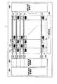
図1は第1の実施の形態による有機EL表示装置の概略を示した説明図である。図1に示されているように,本実施の形態による有機EL表示装置は,表示パネルを形成するための基板1を有し,基板1は,実際に画像を表示する表示領域100,及び画像が表示されない周辺領域を含む。周辺領域には,第1駆動部である選択走査駆動部200,第2及び第3駆動部である発光走査駆動部300,400,及びデータ駆動部500(第4駆動部)が形成されている。(First embodiment)
FIG. 1 is an explanatory diagram showing an outline of the organic EL display device according to the first embodiment. As shown in FIG. 1, the organic EL display device according to the present embodiment includes a
表示領域100は,複数のデータ線D1−Dn,複数の第1走査線である選択走査線S1−Sm,複数の第2及び第3走査線である発光走査線E11−E1m,E21−E2m,及び複数の画素を含む。データ線D1−Dnは列方向に伸びていて,画像を表示するデータ信号を画素に伝達する。選択走査線S1−Sm及び発光走査線E11−E1m,E21−E2mは行方向に伸びていて,各々選択信号及び発光信号を画素に伝達する。そして,1つのデータ線及び1つの選択走査線によって画素領域110が定義され,この画素領域110に2つの画素111,112が形成されている。The
選択走査駆動部200は,複数の選択走査線S1−Smに選択信号を順次に印加し,発光走査駆動部300,400は,複数の発光走査線E11−E1m,E21−E2mに発光信号を順次に印加する。また,データ駆動部500は,データ信号をデータ線D1−Dnに印加する。The selective
本実施の形態によると,各走査駆動部200〜400は,1フレームを2つのフィールドに分割して各走査線を駆動する。具体的には,選択走査駆動部200は,各フィールドで複数の選択走査線S1−Smに選択信号を順次に印加し,発光走査駆動部300は,1つのフィールド(第1フィールド)で複数の発光走査線E11−E1mに発光信号(第1発光信号)を順次に印加し,発光走査駆動部400は,他の1つのフィールド(第2フィールド)で複数の発光走査線E21−E2mに発光信号(第2発光信号)を順次に印加する。According to the present embodiment, each
各走査駆動部200,300,400またはデータ駆動部500の少なくともいずれかは,基板1上に集積回路の形態で直接装着することができる。または,これら各走査駆動部200,300,400またはデータ駆動部500の少なくともいずれかは,基板1上で走査線S1−Sm,E11−E1m,E21−E2m,データ線D1−Dn,及び画素回路110のトランジスタを形成する層と同一層に形成することもできる。At least one of the
または,これら駆動部200,300,400またはデータ駆動部500の少なくともいずれかは,基板1と別途の基板に形成して,これら基板を基板1に電気的に連結することもでき,また,基板1に接着されて電気的に連結されたTCP(tape carrier package),FPC(flexible printed circuit),またはTAB(tape automatic bonding)にチップなどの形態で装着することもできる。 Alternatively, at least one of the driving
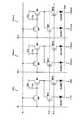
以下,図2を参照して,本実施の形態による画素について詳細に説明する。図2は本実施の形態による画素の概略的な回路図である。図2では,説明の便宜上,i番目の行の走査線Si及びj番目〜(j+2)番目の列のデータ線Dj,Dj+1,Dj+2で各々形成される三つの画素領域110ij,110i(j+1),110i(j+2)に形成される6つの画素111ij,112ij,111i(j+1),112i(j+1),111i(j+2),112i(j+2)を例に挙げて示した(ここで,iは1からmの整数であり,jは1から(n−2)の整数である)。Hereinafter, the pixel according to the present embodiment will be described in detail with reference to FIG. FIG. 2 is a schematic circuit diagram of a pixel according to this embodiment. In FIG. 2, for convenience of explanation, three
また,図2では行方向にR,G,Bの順に画素が配置されるとする。図2に示されているように,画素領域110ijは,選択走査線Si及びデータ線Djによって形成され,2つの画素111ij,112ij(第1,第2画素)を有する。画素111ij,112ijは駆動回路及びデータ線Djを共有し,有機EL素子OLED1,OLED2(発光素子)及び各々スイッチングトランジスタM31,M32,(駆動回路の出力電流を発光素子に伝達するスイッチング素子)を有する。ここで,有機EL素子OLED1,OLED2は各々R及びGの色相の光を発光し,駆動回路については後述する。In FIG. 2, it is assumed that pixels are arranged in the order of R, G, and B in the row direction. As illustrated in FIG. 2, the
画素領域110i(j+1)は選択走査線Si及びデータ線Dj+1によって形成され,2つの画素111i(j+1),112i(j+1)を有する。画素領域110i(j+1)の画素111i(j+1),112i(j+1)も画素111ij,112ijと同一な構造を有し,画素111i(j+1),112i(j+1)の有機EL素子OLED1,OLED2は,各々B及びRの色相の光を発光する。The
画素領域110i(j+2)は選択走査線Si及びデータ線Dj+2によって形成され,2つの画素111i(j+2),112i(j+2)を含む。画素領域110i(j+2)の画素111i(j+2),112i(j+2)も画素111ij,112ijと同一な構造を有し,画素111i(j+2),112i(j+2)の有機EL素子OLED1,OLED2は各々G及びBの色相の光を発光する。The
本実施の形態によると,駆動回路は,駆動トランジスタM1(データ信号に対応する電流を出力するトランジスタ),スイッチングトランジスタM2(データ信号をトランジスタM1に伝達するスイッチング素子),及びキャパシタCstを含み,スイッチングトランジスタM2を通じて記入されるデータ信号に対応する電圧をキャパシタCstが保存し,キャパシタCstに保存された電圧によって駆動トランジスタM1が電源VDDから電流を導通させる。 According to the present embodiment, the drive circuit includes a drive transistor M1 (a transistor that outputs a current corresponding to a data signal), a switching transistor M2 (a switching element that transmits a data signal to the transistor M1), and a capacitor Cst. The voltage corresponding to the data signal written through the transistor M2 is stored in the capacitor Cst, and the driving transistor M1 conducts current from the power supply VDD by the voltage stored in the capacitor Cst.
具体的に,トランジスタM1のソースは電源電圧VDDに連結され,トランジスタM1のソース及びゲートの間にキャパシタCstが連結されている。また,トランジスタM2はデータ線Dj,Dj+1,Dj+2及びトランジスタM1のゲートの間に接続され,ゲートに印加される選択信号に応答してデータ信号をトランジスタM1のゲートに伝達する。Specifically, the source of the transistor M1 is connected to the power supply voltage VDD, and the capacitor Cst is connected between the source and gate of the transistor M1. Further, the transistor M2 is connected between the gate of the data linesD j, D j + 1, D j + 2 and the transistors M1, transmit data signals to the gate of the transistor M1 in response to a selection signal applied to the gate.
トランジスタM31,M32は,トランジスタM1のドレイン及び有機EL素子OLED1,OLED2に各々連結され,発光走査線E1i,E2iからの発光信号に応答してトランジスタM1の出力電流を有機EL素子OLED1,OLED2に伝達する。有機EL素子OLEDのカソードは電源電圧VSSに連結されており,電源電圧VSSは電源電圧VDDより低い電圧で,一般に負の電圧,接地電圧などを使用する。The transistors M31 and M32 are connected to the drain of the transistor M1 and the organic EL elements OLED1 and OLED2, respectively, and output current of the transistor M1 in response to the light emission signals from the light emission scanning lines E1i and E2i. To communicate. The cathode of the organic EL element OLED is connected to the power supply voltage VSS, and the power supply voltage VSS is lower than the power supply voltage VDD, and generally uses a negative voltage, a ground voltage, or the like.
これにより,選択走査線Siに低レベルの選択信号が印加されれば,トランジスタM2を通じてデータ電圧がトランジスタM1のゲートに伝達され,トランジスタM1のゲート及びソースの間には電源電圧VDDとデータ電圧との差に相当する電圧VSGが印加される。また,この電圧VSGがキャパシタCstに充電される。Thus, if a low level selection signal is applied to the selection scan line Si, a data voltage through the transistor M2 is transmitted to the gate of the transistor M1, the power supply voltage VDD and the data voltage is formed between the gate of the transistor M1 and the source A voltage VSG corresponding to the difference between the two is applied. Further, this voltage VSG is charged in the capacitor Cst.
その後,発光走査線E1iに低レベルの発光信号が印加されれば,トランジスタM31が導通してトランジスタM1から有機EL素子OLED1に数式1のような電流IOLEDが印加される。したがって,有機EL素子OLED1は電流IOLEDの大きさに対応する光の強さで発光する。同様に,発光走査線E2iに低レベルの発光信号が印加されれば,トランジスタM32が導通して有機EL素子OLED2が発光する。つまり,1フレームの2つのフィールドで有機EL素子OLED1,OLED2が,各々1度ずつ発光して色相が表示される。Thereafter, when a low-level light emission signal is applied to the light emission scanning line E1i , the transistor M31 is turned on, and a current IOLED as expressed by

ここで,βは定数であり,VSGはトランジスタM1のソース−ゲート電圧であり,VTHはトランジスタM1のしきい電圧である。Here, β is a constant, VSG is the source-gate voltage of the transistor M1, and VTH is the threshold voltage of the transistor M1.
以下,図3〜図4Bを参照して,本実施の形態による有機EL表示装置の駆動方法について詳細に説明する。図3は本実施の形態による有機EL表示装置の駆動タイミング図であり,図4A及び図4nは各々第1フィールド及び第2フィールドで点灯する画素を示した図面である。 Hereinafter, a method for driving the organic EL display device according to the present embodiment will be described in detail with reference to FIGS. FIG. 3 is a driving timing chart of the organic EL display device according to the present embodiment, and FIGS. 4A and 4n are diagrams showing pixels that are lit in the first field and the second field, respectively.
図3では,選択走査線Siに印加される選択信号をselect[i]で示し,発光走査線E1i,E2iに印加される発光信号を各々emit1[i]及びemit2[i]で示した(ここで,iは1からmまでの整数)。そして,データ線D1−Dnには同時にデータ電圧が印加されるので,図3では,j番目のデータ線Djに印加されるデータ電圧のみをdata[j]で示した。In Figure 3, shows a select signal applied to the selection scan lineS i in the select [i] indicates the emit scan linesE1i, a light-emitting signal applied toE 2i each emit1 in [i] and Emit2 [i] (Where i is an integer from 1 to m). Since the data voltage is simultaneously applied to the data lines D1 to Dn , only the data voltage applied to thejth data line Dj is indicated by data [j] in FIG.
図3に示されているように,本実施の形態による有機EL表示装置は,1フレームが2つのフィールド1F,2Fに分割されて駆動され,各フィールド1F,2Fで選択走査線S1−Smに低レベルの選択信号select[1]−select[m]が順次に印加される。駆動回路を共有する2つの画素の有機EL素子OLED1,OLED2は,各々1つのフィールドに相当する期間の間発光する。そして,フィールド1F,2Fは行別に独立的に定義され,図3では第1行の選択走査線S1を基準に2つのフィールド1F,2Fを示した。As shown in FIG. 3, the organic EL display device according to the present embodiment is driven by dividing one frame into two
第1フィールド1Fで選択走査線S1に印加される選択信号select[1]が低レベルパルスになり,第1行の各画素領域に含まれた有機EL素子OLED1に対応するデータ電圧data[j]がデータ線Djに伝達される。そして,発光走査線E11の発光信号emit1[1]が低レベルパルスになってトランジスタM31が導通する。その結果,第1行の画素領域でデータ電圧data[j]に対応する電流がトランジスタM1のドレインに出力され,トランジスタM31はトランジスタM1の出力電流を有機EL素子OLED1に伝達する。Selection signal the select [1] applied to the selection scan linesS 1 in the
したがって,有機EL素子OLED1は印加される電流に対応して発光し,有機EL素子OLED1の発光は発光信号emit1[1]が低レベルを維持する間持続する。本実施の形態によれば,発光信号emit1[1]の低レベルパルス幅は第1フィールド1Fの期間と実質的に同一である。 Therefore, the organic EL element OLED1 emits light corresponding to the applied current, and the light emission of the organic EL element OLED1 is continued while the light emission signal emit1 [1] is maintained at a low level. According to the present embodiment, the low-level pulse width of the light emission signal emit1 [1] is substantially the same as the period of the
次に,選択走査線S2の選択信号select[2]が低レベルパルスになり,第2行の各画素領域の有機EL素子OLED1に対応するデータ電圧data[j]がデータ線Djに印加される。そして,発光走査線E12の発光信号emit1[2]が低レベルパルスになってトランジスタM31が導通する。その結果,第2行画素領域の有機EL素子OLED1が発光信号emit1[2]の低レベルパルス期間の間発光する。Next, selection of the selection signal select scan lineS 2 [2] becomes the low level pulse, applying the data voltage data corresponding to the organic EL element OLED1 in each pixel area of the second row [j] to the data linesD j Is done. Then, light emission signals of the light-emitting scan linesE 12 emit1 [2] the transistor M31 is turned on in a low-level pulse. As a result, the organic EL element OLED1 in the second row pixel region emits light during the low-level pulse period of the light emission signal emit1 [2].
このように,第1番目からm番目の行の選択走査線S1−Smに低レベルパルスを有する選択信号select[1]−select[m]が順次に印加される。そして,i番目の行の選択走査線Siの選択信号select[i]が低レベルパルスである間に各画素領域の有機EL素子OLED1に対応するデータ電圧data[j]がデータ線Djに印加される。Thus, the select signal the select [1] with a low level pulse -select [m] are sequentially applied to the selection scan lineS 1 -Sm of the m-th row from the first. Then, the data voltage i-th row of the selection scan lineS i of the selection signal the select [i] corresponds to the organic EL element OLED1 in each pixel region during a low-level pulse data [j] to the data linesD j Applied.
そして,選択走査線Siの選択信号select[i]が低レベルパルスになる時に,i番目の行の2つの発光走査線E1i,E2iのうちの発光走査線E1iの発光信号emit1[i]が低レベルパルスになり,発光信号emit1[i]の低レベルパルス幅は第1フィールド1Fの期間と同一である。その結果,各行では選択走査線Siの選択信号select[i]が低レベルパルスになった後で,第1フィールド1Fに相当する期間の間有機EL素子OLED1が発光する。When the selection signal select [i] of the selection scanning line Si becomes a low level pulse, the light emission signal emit1 [i] of the light emission scanning line E1i of the two light emission scanning lines E1i and E2i of the i-th row. ] Becomes a low level pulse, and the low level pulse width of the light emission signal emit1 [i] is the same as the period of the
つまり,本実施の形態によれば,第1フィールドで各行の有機EL素子OLED1が発光し,結局,図4Aに示されているように,各行で1つのデータ線を共有して行方向に隣接する2つの画素のうちデータ線の左側に形成された画素(第1グループの画素)のみが発光する。 That is, according to the present embodiment, the organic EL elements OLED1 in each row emit light in the first field, and eventually, as shown in FIG. 4A, each row shares one data line and is adjacent in the row direction. Of the two pixels, only the pixel (first group of pixels) formed on the left side of the data line emits light.
第2フィールド2Fで選択走査線S1の選択信号select[1]が低レベルパルスになり,第1行の各画素領域の有機EL素子OLED2に対応するデータ電圧data[j]がデータ線Djに印加される。そして,発光走査線E21の発光信号emit2[1]が低レベルパルスになってトランジスタM32が導通する。Selection signal the select [1] is selected scan linesS 1 goes low pulse in the
その結果,有機EL素子OLED2が発光し,有機EL素子OLED2の発光は発光信号emit2[1]の低レベルパルス期間の間持続する。本実施の形態によれば,発光信号emit2[1]の低レベルパルスの幅は第2フィールド2Fの期間と実質的に同一である。 As a result, the organic EL element OLED2 emits light, and the light emission of the organic EL element OLED2 lasts for the low-level pulse period of the light emission signal emit2 [1]. According to the present embodiment, the width of the low level pulse of the light emission signal emit2 [1] is substantially the same as the period of the
次に,選択走査線S2の選択信号select[2]が低レベルパルスになり,第2行の各画素領域の有機EL素子OLED2に対応するデータ電圧data[j]がデータ線Djに印加され,第2行の発光走査線E22の発光信号emit2[2]が低レベルパルスになってトランジスタM32が導通する。その結果,第2行の画素領域の有機EL素子OLED2が発光信号emit2[2]の低レベルパルス期間の間発光する。Next, selection of the selection signal select scan lineS 2 [2] becomes the low level pulse, applying the data voltage data corresponding to the organic EL element OLED2 in each pixel area of the second row [j] to the data linesD j is, light emission signals emit2 the second row of light-emitting scan linesE 22 [2] is the transistor M32 is turned on in a low-level pulse. As a result, the organic EL element OLED2 in the pixel region of the second row emits light during the low level pulse period of the light emission signal emit2 [2].
このように,第2フィールド2Fでも第1番目からm番目の行の選択走査線S1−Smの選択信号select[1]−select[m]が順次に低レベルパルスになる。i番目の行の選択走査線Siの選択信号select[i]が低レベルパルスである間に,各画素領域の有機EL素子OLED2に対応するデータ電圧data[j]がデータ線Djに印加される。Thus, m-th selection signal the select [1] of the selection scan linesS 1 -Sm row -select [m] is sequentially become low level pulse from the first even
そして,選択走査線Siの選択信号select[i]が低レベルパルスになる時に,i番目の行の二つの発光走査線E1i,E2iのうちの発光走査線E2iの発光信号emit2[i]が低レベルパルスになり,発光信号emit2[i]の低レベルパルス幅は第2フィールド2Fの期間と同一である。その結果,各行では選択走査線Siの選択信号select[i]が低レベルパルスになった後で,第2フィールド1Fに相当する期間の間有機EL素子OLED2が発光する。When the selection signal select [i] of the selection scanning line Si becomes a low level pulse, the light emission signal emit2 [2] of the light emission scanning line E2i of the two light emission scanning lines E1i and E2i of the i-th row. i] becomes a low level pulse, and the low level pulse width of the light emission signal emit2 [i] is the same as the period of the
つまり,本実施の形態によれば,第2フィールドで各行の有機EL素子OLED2が発光し,結局,図4Bに示されているように,各行で1つのデータ線を共有して行方向に隣接する2つの画素のうちデータ線の右側に形成された画素(第2グループの画素)のみが発光する。 That is, according to the present embodiment, the organic EL elements OLED2 in each row emit light in the second field, and eventually, as shown in FIG. 4B, each row shares one data line and is adjacent in the row direction. Of the two pixels, only the pixels (second group of pixels) formed on the right side of the data line emit light.
このように,本実施の形態による有機EL表示装置は,1フレームが2つのフィールドに分割されて駆動され,1つのフィールドで各画素領域の2つの画素のうちの1つの画素の有機EL素子のみが発光する。そして,他のフィールドで2つの画素のうちの残りの画素の有機EL素子が発光して,1フレームで全ての画素の有機EL素子が発光することができ,そのために全ての色相が表示できる。 As described above, the organic EL display device according to the present embodiment is driven by dividing one frame into two fields, and only one organic EL element of one pixel out of two pixels in each pixel region in one field. Emits light. Then, the organic EL elements of the remaining pixels of the two pixels emit light in the other field, and the organic EL elements of all the pixels can emit light in one frame, so that all hues can be displayed.
また,2つの画素が駆動回路及びデータ線Djを共有することによって,データ線Dj及び駆動回路の個数を従来の技術に比べて半分に減少させることができる。したがって,データ線Djを駆動するための集積回路の個数を減少させることができ,また,画素領域で素子の配置を簡単にすることができる。Further, since the two pixels share the drive circuit and the data line Dj , the number of the data line Dj and the drive circuit can be reduced by half compared to the conventional technique. Therefore, it is possible to reduce the number of integrated circuits for driving the data lines Dj, also it is possible to simplify the arrangement of the elements in the pixel region.
しかし,本実施の形態のように各フィールドで同一列の画素を点灯させる場合,各々のフィールドで発光しない画素のパターンが表示パネル上に瞬間的に現れる問題があった。つまり,第1フィールドでは1つのデータ線を共有して行方向に隣接する画素のうちの左側に形成された画素(つまり,有機EL素子OLED1)が発光し,第2フィールドではデータ線の右側に形成された画素(つまり,有機EL素子OLED2)が発光することによって,第1フィールドから第2フィールドへ進む場合に,1つの列の画素が同時に点灯したり消灯されたりすることによって,パネル上に縦縞が現れる現象が発生するのである。 However, when pixels in the same column are lit in each field as in this embodiment, there is a problem that a pattern of pixels that do not emit light in each field appears instantaneously on the display panel. That is, in the first field, a pixel (that is, the organic EL element OLED1) formed on the left side of pixels adjacent in the row direction sharing one data line emits light, and in the second field, on the right side of the data line. When the formed pixel (that is, the organic EL element OLED2) emits light and proceeds from the first field to the second field, the pixels in one column are turned on or off at the same time on the panel. A phenomenon in which vertical stripes appear occurs.
(第2の実施の形態)
したがって,第2の実施の形態では,第1フィールド及び第2フィールドで上下左右方向に互いに隣接する複数の発光画素の間に,非発光画素が少なくとも1つ存在するようにして,表示パネルに縦縞が現れる問題を解決するものである。(Second Embodiment)
Therefore, in the second embodiment, vertical stripes are formed on the display panel such that at least one non-light-emitting pixel exists between a plurality of light-emitting pixels adjacent to each other vertically and horizontally in the first field and the second field. It solves the problem that appears.
以下,図5〜図6Bを参照して,第2の実施の形態による表示装置について説明する。図5は本実施の形態による表示装置を概略的に示した説明図であり,図6A及び図6Bは,各々第1及び第2フィールドで点灯する画素を示した説明図である。 Hereinafter, a display device according to the second embodiment will be described with reference to FIGS. FIG. 5 is an explanatory diagram schematically showing the display device according to the present embodiment, and FIGS. 6A and 6B are explanatory diagrams showing pixels that are lit in the first and second fields, respectively.
第2の実施の形態による表示装置は,奇数番目の行の発光走査線E1(2i−1),E2(2i−1)の連結関係及び偶数番目の行の発光走査線E1(2i),E2(2i)の連結関係が互いに変化するという点で,第1の実施の形態による表示装置と異なる。In the display device according to the second embodiment, the connection relationship between the odd-numbered rows of light emission scanning lines E1 (2i-1) and E2 (2i-1) and the even-numbered rows of light emission scanning lines E1 (2i). ) , E2 (2i) is different from the display device according to the first embodiment in that the connection relationship changes.
具体的に,第1行では発光走査線E11が画素領域110で左側画素111に連結されており,発光走査線E21が右側画素112に連結されている。そして,第2行では発光走査線E12が画素領域110で右側画素112に連結されており,発光走査線E22が左側画素111に連結されている。Specifically, in the first row, the light emission scanning line E11 is connected to the
つまり,第2の実施の形態によれば,奇数番目の行では発光走査線E1iが左側画素111に連結され,発光走査線E2iが右側画素112に連結され,偶数番目の行ではこれと反対に連結される。In other words, according to the second embodiment, the light emission scanning line E1i is connected to the
このように構成する場合,第1フィールド1Fでは,図6Aのように,奇数番目の行の画素領域110(第1グループの第1走査線によって定義される画素領域)に形成された左側画素111及び偶数番目の行の画素領域110に形成された右側画素112が発光し,第2フィールド2Fでは,図6Bのように,奇数番目の行の画素領域110(第2グループの第1走査線によって定義される画素領域)に形成された右側画素112及び偶数番目の行の各画素領域110に形成された左側画素111が発光する。 In the case of such a configuration, in the
したがって,上下または左右方向に隣接する任意の2つの発光画素の間に非発光画素が少なくとも1つ存在して,同一列または同一行の画素が同時に点灯または消灯されないようになる。したがって,表示パネルに現れる縦縞が除去され,表示装置の画質が改善される。 Therefore, at least one non-light emitting pixel exists between any two light emitting pixels adjacent in the vertical or horizontal direction, so that pixels in the same column or the same row are not turned on or off at the same time. Therefore, vertical stripes appearing on the display panel are removed, and the image quality of the display device is improved.
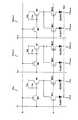
以下,図7A及び図7Bを参照して,第2の実施の形態による画素について詳細に説明する。図7Aは奇数番目の行の画素領域に含まれる6つの画素を示した図面であり,図7Bは偶数番目の行の画素領域に含まれる6つの画素を示した説明図である。 Hereinafter, the pixel according to the second embodiment will be described in detail with reference to FIGS. 7A and 7B. FIG. 7A is a diagram showing six pixels included in the pixel regions of the odd-numbered rows, and FIG. 7B is an explanatory diagram showing six pixels included in the pixel regions of the even-numbered rows.
図7Aに示されているように,奇数番目の行の画素領域110ij,110i(j+1),110i(j+2)に形成された画素のうちの左側画素111ij,111i(j+1),111i(j+2)のトランジスタM31のゲートが発光走査線E1iに連結され,右側画素112ij,112i(j+1),112i(j+2)のトランジスタM32のゲートが発光走査線E2iに連結される。As shown in FIG. 7A, the
したがって,第1フィールドで発光走査線E11−E1mに発光信号が順次に印加されれば,奇数番目の行に形成された画素領域110の左側画素が発光し,第2フィールドで発光走査線E21−E2mに発光信号が順次に印加されれば,奇数番目の行に形成された画素領域110の右側画素が発光する。Accordingly, if the light emission signals are sequentially applied to the light emission scanning lines E11 to E1m in the first field, the left pixel of the
また,図7Bに示されているように,偶数番目の行の画素領域110ij,110i(j+1),110i(j+2)に形成された画素のうちの右側画素112ij,112i(j+1),112i(j+2)のトランジスタM42(駆動回路の出力電流を発光素子に伝達するスイッチング素子)のゲートが発光走査線E1iに連結され,左側画素111ij,111i(j+1),111i(j+2)のトランジスタM41(駆動回路の出力電流を発光素子に伝達するスイッチング素子)のゲートが発光走査線E2iに連結される。Further, as shown in FIG. 7B,
したがって,第1フィールドで発光走査線E11−E1mに発光信号が順次に印加されれば,偶数番目の行の画素領域110のうちの右側画素が発光し,第2フィールドで発光走査線E21−E2mに発光信号が順次に印加されれば,偶数番目の行の画素領域110のうちの左側画素が発光する。Accordingly, if the light emission signal is sequentially applied to the light emission scanning lines E11 to E1m in the first field, the right pixel in the
(第3の実施の形態)
図8A及び図8Bは第3の実施の形態による画素回路を示した説明図であって,図8Aは奇数番目の行に形成された画素を示しており,図8Bは偶数番目の行に形成された画素を示している。(Third embodiment)
8A and 8B are explanatory diagrams showing a pixel circuit according to the third embodiment. FIG. 8A shows pixels formed in odd-numbered rows, and FIG. 8B shows pixels formed in even-numbered rows. The shown pixels are shown.
第3の実施の形態による画素は,画素に含まれたトランジスタM51,M52,及びM61,M62(駆動回路の出力電流を発光素子に伝達するスイッチング素子)が互いに異なるタイプのチャンネルを有するように形成され,トランジスタM51,M52,及びM61,M62のゲートが同一な発光走査線Eiを連結するという点で,第1及び第2の実施の形態による画素と異なる。The pixel according to the third embodiment is formed so that the transistors M51, M52, and M61, M62 (switching elements that transmit the output current of the drive circuit to the light emitting elements) included in the pixels have different types of channels. The transistors M51, M52, and M61, M62 are different from the pixels according to the first and second embodiments in that the gates of the same light emission scanning linesEi are connected.
具体的に,図8Aに示されているように,奇数番目の行の画素領域(第1グループの画素領域)に形成された画素のうちの左側画素に含まれた画素のトランジスタM51をPチャンネルトランジスタで形成し,右側画素に含まれたトランジスタM52をNチャンネルトランジスタで形成した後,発光走査線Eiに図3の発光信号emit1[1]−emit1[m](第1レベルの発光信号)を印加する。Specifically, as shown in FIG. 8A, the transistor M51 of the pixel included in the left pixel among the pixels formed in the pixel region (first group pixel region) in the odd-numbered row is connected to the P channel. forming a transistor, after the transistor M52 included in the right pixel is formed by N-channel transistor, the light emitting signal emit1 of 3 to the emission scan lineE i [1] -emit1 [m ] ( emission signal of the first level) Is applied.
その結果,第1フィールドではトランジスタM51が導通してトランジスタM1の電流が有機EL素子OLED1に伝達され,第2フィールドではトランジスタM52が導通してトランジスタM1の電流が有機EL素子OLED2に伝達される。 As a result, in the first field, the transistor M51 is turned on and the current of the transistor M1 is transmitted to the organic EL element OLED1, and in the second field, the transistor M52 is turned on and the current of the transistor M1 is transmitted to the organic EL element OLED2.
また,図8Bに示されているように,偶数番目の行の画素領域(第2グループの画素領域)に形成された画素のうちの右側画素に含まれた画素のトランジスタM62をPチャンネルトランジスタで形成し,左側画素に含まれたトランジスタM61をNチャンネルトランジスタで形成した後,発光走査線Eiに図3の発光信号emit1[1]−emit1[m](第2レベルの発光信号)を印加する。Further, as shown in FIG. 8B, a pixel transistor M62 included in the right pixel among the pixels formed in the pixel region (second group pixel region) in the even-numbered row is a P-channel transistor. formed, applied after the transistor M61 included in the left pixel and an N-channel transistor, the light emitting signal emit1 of 3 to the emission scan lineE i [1] -emit1 [m ] (the emission signal of a second level) To do.
その結果,第1フィールドではトランジスタM62が導通してトランジスタM1の電流が有機EL素子OLED2に伝達され,第2フィールドではトランジスタM61が導通してトランジスタM1の電流が有機EL素子OLED1に伝達される。 As a result, in the first field, the transistor M62 is turned on and the current of the transistor M1 is transmitted to the organic EL element OLED2, and in the second field, the transistor M61 is turned on and the current of the transistor M1 is transmitted to the organic EL element OLED1.
したがって,第1フィールドでは奇数番目の行の画素領域に形成された画素のうちの左側画素及び偶数番目の行の画素領域に形成された画素のうちの右側画素が発光し,第2フィールドでは奇数番目の行の画素領域に形成された画素のうちの右側画素及び偶数番目の行の画素領域に形成された画素のうちの左側画素が発光する。 Accordingly, in the first field, the left side pixel among the pixels formed in the pixel area of the odd-numbered row and the right side pixel among the pixels formed in the pixel area of the even-numbered row emit light, and the odd number in the second field. The right pixel among the pixels formed in the pixel region of the th row and the left pixel of the pixels formed in the pixel region of the even number row emit light.
本実施の形態によれば,第1フィールドでは画素領域に形成された第1グループの画素を発光信号によって発光させ,第2フィールドでは第2グループの画素を発光させるが,各フィールドで発光画素の間に少なくとも1つの非発光画素が存在するように第1グループ及び第2グループを設定することによって,表示パネルに現れる縦縞を除去することができる。また,2つの発光走査駆動部300,400を1つにすることができ,配線をさらに半減できる効果がある。 According to the present embodiment, in the first field, the first group of pixels formed in the pixel region is caused to emit light by the light emission signal, and in the second field, the second group of pixels is caused to emit light. By setting the first group and the second group so that at least one non-light emitting pixel exists between them, vertical stripes appearing on the display panel can be removed. Moreover, the two light emission
以上,添付図面を参照しながら本発明の好適な実施形態について説明したが,本発明は係る例に限定されないことは言うまでもない。当業者であれば,特許請求の範囲に記載された範疇内において,各種の変更例または修正例に想到し得ることは明らかであり,それらについても当然に本発明の技術的範囲に属するものと了解される。 As mentioned above, although preferred embodiment of this invention was described referring an accompanying drawing, it cannot be overemphasized that this invention is not limited to the example which concerns. It will be apparent to those skilled in the art that various changes and modifications can be made within the scope of the claims, and these are of course within the technical scope of the present invention. Understood.
第2及び第3の実施の形態では,奇数番目の行の画素及び偶数番目の行の画素が第1フィールド及び第2フィールドで発光走査線に連結される関係を互いに変更すると説明したが,本発明の範囲がこれに限定されるわけではなく,実施例に応じて,多様な方法で,各フィールドで発光画素の間に少なくとも一つの非発光画素が存在するように画素の連結関係を変更することができる。 In the second and third embodiments, it has been described that the relationship in which the pixels in the odd-numbered rows and the pixels in the even-numbered rows are connected to the light emission scanning lines in the first field and the second field is changed. The scope of the invention is not limited to this, and the connection relationship of the pixels is changed by various methods so that at least one non-light emitting pixel exists in each field according to the embodiment. be able to.
また,第1〜第3の実施の形態では,1つの画素領域に2つの画素を形成し,1フレームを2つのフィールドに分けて駆動すると説明したが,実施例に応じては,1つの画素領域に3つの画素を形成し,1フレームを3つのフィールドに分けて駆動することもできる。 In the first to third embodiments, it has been described that two pixels are formed in one pixel region and one frame is divided into two fields and driven. However, depending on the embodiment, one pixel is used. Three pixels can be formed in the region, and one frame can be divided into three fields for driving.
本発明は,表示装置,表示パネル及び表示装置の駆動方法に適用可能であり,特に駆動回路を減少させ,画素の開口率を増加させることができる有機電界発光表示装置,表示パネル及び表示装置の駆動方法に適用可能である。 The present invention can be applied to a display device, a display panel, and a driving method of the display device, and in particular, an organic light emitting display device, a display panel, and a display device capable of reducing a driving circuit and increasing a pixel aperture ratio. It can be applied to a driving method.
1 基板
100 表示領域
110 画素領域
111 画素
112 画素
200 選択走査駆動部
300 発光走査駆動部
400 発光走査駆動部
500 データ駆動部
D1−Dn データ線
E11−E1m 発光走査線
E21−E2m 発光走査線
S1−Sm 選択走査線
Cst キャパシタ
M1 駆動トランジスタ
M2 スイッチングトランジスタ
M31 トランジスタ
M32 トランジスタ
OLED1 有機EL素子
OLED2 有機EL素子
1
Claims (15)
Translated fromJapanese1フレームを構成する複数のフィールドで,各々選択信号を前記複数の第1走査線に順次に伝達する第1駆動部と,
前記複数のフィールドのうちの第1フィールドで,前記第1発光信号を前記複数の第2走査線に順次に伝達する第2駆動部と,
前記複数のフィールドのうちの第2フィールドで,前記第2発光信号を前記複数の第3走査線に順次に伝達する第3駆動部と,
を備え,
前記画素領域には,前記データ線及び前記第1走査線を共有する少なくとも2つの画素が形成され,
前記第1フィールドでは前記画素領域に形成された画素のうちの第1グループの画素が前記第1発光信号によって発光し,前記第2フィールドでは第2グループの画素が前記第2発光信号によって発光し,
前記画素領域は,第1側に形成されている第1画素と第2側に形成されている第2画素とを含み,
前記第1グループの画素は,奇数番目の第1走査線によって形成される画素領域の前記第1画素と,偶数番目の第1走査線によって形成される画素領域の前記第2画素とを含み,
前記第2グループの画素は,奇数番目の第1走査線によって形成される画素領域の第2画素と,偶数番目の第1走査線によって形成される画素領域の前記第1画素とを含み、
前記第1側は左側であり,前記第2側は右側であることを特徴とする発光表示装置。A plurality of data lines for transmitting data signals for displaying an image; a plurality of first scanning lines for transmitting selection signals; a plurality of second and third scanning lines for transmitting first and second light emission signals; A display region having a plurality of pixel regions each defined by the data line and the first scan line;
A first driver for sequentially transmitting a selection signal to each of the plurality of first scanning lines in a plurality of fields constituting one frame;
A second driver for sequentially transmitting the first light emission signal to the plurality of second scanning lines in a first field of the plurality of fields;
A third driving unit for sequentially transmitting the second light emission signal to the plurality of third scanning lines in a second field of the plurality of fields;
With
In the pixel region, at least two pixels sharing the data line and the first scan line are formed,
In the first field, among the pixels formed in the pixel region, a first group of pixels emits light by the first light emission signal, and in the second field, a second group of pixels emits light by the second light emission signal. ,
The pixel region includes a first pixel formed on the first side and a second pixel formed on the second side,
The first group of pixels includes the first pixel in a pixel region formed by an odd-numbered first scan line and the second pixel in a pixel region formed by an even-numbered first scan line,
The pixels of the second group areseen including a second pixel of the pixel region formed by the odd-numbered first scan line, and the first pixel of the pixel region formed by the even-numbered first scanline,
The light emitting display device,wherein the first side is a left side and the second side is a right side .
前記データ信号に対応する電流を出力する駆動回路を共有し,
印加される電流に対応して光を放出する発光素子と,
前記第1及び第2発光信号に応答して前記駆動回路の出力電流を前記発光素子に伝達するスイッチング素子と,
を各々有することを特徴とする請求項1または2に記載の発光表示装置。The first and second pixels are:
Sharing a drive circuit for outputting a current corresponding to the data signal;
A light emitting device that emits light in response to an applied current;
A switching element for transmitting an output current of the drive circuit to the light emitting element in response to the first and second light emission signals;
The light-emitting display device according to claim 1, further comprising:
前記データ信号に対応する電流を出力するトランジスタと,
前記選択信号に応答して前記データ信号を前記トランジスタに伝達するスイッチング素子と,
前記トランジスタのソース及びゲート間の電圧を一定の期間維持させるキャパシタと,
を有することを特徴とする請求項3に記載の発光表示装置。The drive circuit is
A transistor that outputs a current corresponding to the data signal;
A switching element for transmitting the data signal to the transistor in response to the selection signal;
A capacitor for maintaining a voltage between a source and a gate of the transistor for a certain period;
The light-emitting display device according to claim 3.
1フレームを構成する複数のフィールドで,各々選択信号を前記複数の第1走査線に順次に伝達する第1駆動部と,
前記複数のフィールドのうちの第1フィールドで,前記第1レベルの発光信号を前記複数の第2走査線に順次に伝達し,第2フィールドで,前記第2レベルの発光信号を前記複数の第2走査線に順次に伝達する第2駆動部と,
を備え,
前記画素領域には,前記データ線及び前記第1走査線を共有する少なくとも2つの画素が形成され,
前記第1フィールドでは前記画素領域に形成された画素のうちの第1のグループの画素が前記第1レベルの発光信号によって発光し,前記第2フィールドでは第2のグループの画素が前記第2レベルの発光信号によって発光し,
前記画素領域は,第1側に形成されている第1画素と第2側に形成されている第2画素とを含み,
前記第1グループの画素は,奇数番目の第1走査線によって形成される画素領域の前記第1画素と,偶数番目の第1走査線によって形成される画素領域の前記第2画素とを含み,
前記第2グループの画素は,奇数番目の第1走査線によって形成される画素領域の第2画素と,偶数番目の第1走査線によって形成される画素領域の前記第1画素とを含み、
前記第1側は左側であり,前記第2側は右側であることを特徴とする発光表示装置。A plurality of data lines for transmitting a data signal for displaying an image, a plurality of first scanning lines for transmitting a selection signal, and a plurality of second scanning lines for transmitting a light emission signal having first and second level voltages; A display area having a plurality of pixel areas respectively defined by the data lines and the first scan lines;
A first driver for sequentially transmitting a selection signal to each of the plurality of first scanning lines in a plurality of fields constituting one frame;
The first level light emission signal is sequentially transmitted to the plurality of second scanning lines in a first field of the plurality of fields, and the second level light emission signal is transmitted to the plurality of second scanning lines in a second field. A second driving unit for sequentially transmitting to two scanning lines;
With
In the pixel region, at least two pixels sharing the data line and the first scan line are formed,
In the first field, a first group of pixels formed in the pixel region emits light by the first level light emission signal, and in the second field, a second group of pixels is the second level. Emits light by the light emission signal of
The pixel region includes a first pixel formed on the first side and a second pixel formed on the second side,
The first group of pixels includes the first pixel in a pixel region formed by an odd-numbered first scan line and the second pixel in a pixel region formed by an even-numbered first scan line,
The pixels of the second group areseen including a second pixel of the pixel region formed by the odd-numbered first scan line, and the first pixel of the pixel region formed by the even-numbered first scanline,
The light emitting display device,wherein the first side is a left side and the second side is a right side .
前記データ信号に対応する電流を出力する駆動回路を共有し,
印加される電流に対応して光を放出する発光素子と,
前記発光信号に応答して前記駆動回路の出力電流を前記発光素子に伝達するスイッチング素子と,
を各々有することを特徴とする請求項5に記載の発光表示装置。The first and second pixels are:
Sharing a drive circuit for outputting a current corresponding to the data signal;
A light emitting device that emits light in response to an applied current;
A switching element for transmitting an output current of the drive circuit to the light emitting element in response to the light emission signal;
The light-emitting display device according to claim5 .
前記データ信号に対応する電流を出力するトランジスタと,
前記選択信号に応答して前記データ信号を前記トランジスタに伝達するスイッチング素子と,
前記トランジスタのソース及びゲート間の電圧を一定の期間維持させるキャパシタと,
を有することを特徴とする請求項6に記載の発光表示装置。The drive circuit is
A transistor that outputs a current corresponding to the data signal;
A switching element for transmitting the data signal to the transistor in response to the selection signal;
A capacitor for maintaining a voltage between a source and a gate of the transistor for a certain period;
The light emitting display device according to claim6 .
第1フィールド及び第2フィールドで各々選択信号を伝達する複数の第1走査線と,
前記第1フィールドで第1発光信号を伝達する複数の第2走査線と,
前記第2フィールドで第2発光信号を伝達する複数の第3走査線と,
前記データ線及び前記第1走査線によって各々定義され,前記データ線及び前記第1走査線を共有する第1及び第2画素が形成される複数の画素領域と,
を備え,
前記画素領域で,前記第1画素は第1側に形成され,前記第2画素は第2側に形成され,
前記複数の第1走査線のうちの第1グループの第1走査線によって定義される前記画素領域の前記第1画素は前記第1発光信号によって発光し,前記第2画素は前記第2発光信号によって発光し,
前記複数の第1走査線のうちの第2グループの第1走査線によって定義される前記画素領域の前記第1画素は前記第2発光信号によって発光し,前記第2画素は前記第1発光信号によって発光し、
前記第1側は左側であり,前記第2側は右側であることを特徴とする,表示パネル。A plurality of data lines for transmitting data signals for displaying images;
A plurality of first scan lines for transmitting a selection signal in each of the first field and the second field;
A plurality of second scanning lines transmitting a first light emission signal in the first field;
A plurality of third scan lines transmitting a second light emission signal in the second field;
A plurality of pixel regions, each defined by the data line and the first scan line, in which first and second pixels sharing the data line and the first scan line are formed;
With
In the pixel region, the first pixel is formed on the first side, the second pixel is formed on the second side,
The first pixel of the pixel region defined by the first scan line of the first group of the plurality of first scan lines emits light by the first light emission signal, and the second pixel emits the second light emission signal. Emits light by
The first pixel of the pixel region defined by a first scan line of a second group of the plurality of first scan lines emits light by the second light emission signal, and the second pixel emits the first light emission signal.emit lightby,
The display panel according toclaim 1, wherein the first side is the left side and the second side is the right side .
前記データ線を駆動するための第4駆動部と,
をさらに含むことを特徴とする請求項9または10に記載の表示パネル。A first drive unit, a second drive unit, and a third drive unit for driving the first scan line, the second scan line, and the third scan line;
A fourth driving unit for driving the data line;
The display panel according to claim9 , further comprising:
第1フィールド及び第2フィールドで各々選択信号を伝達する複数の第1走査線と,
前記第1フィールドで第1レベルの発光信号を伝達し,前記第2フィールドで第2レベルの発光信号を伝達する複数の第2走査線と,
前記データ線及び前記第1走査線によって各々定義され,前記データ線及び前記第1走査線を共有する第1及び第2画素が形成される複数の画素領域と,
を備え,
前記第1画素は前記第1レベルの発光信号によって発光し,前記第2画素は前記第2レベルの発光信号によって発光し,
前記複数の画素領域のうちの第1グループの画素領域及び第2グループの画素領域において,前記第1画素は左側に形成され、前記第2画素は右側に形成されることを特徴とする,表示パネル。A plurality of data lines for transmitting data signals for displaying images;
A plurality of first scan lines for transmitting a selection signal in each of the first field and the second field;
A plurality of second scan lines transmitting a first level light emission signal in the first field and transmitting a second level light emission signal in the second field;
A plurality of pixel regions, each defined by the data line and the first scan line, in which first and second pixels sharing the data line and the first scan line are formed;
With
The first pixel emits light by the first level light emission signal, the second pixel emits light by the second level light emission signal,
In the first group of pixel regions and the second group of pixel regions of theplurality of pixel regions,the first pixel is formed on the left side, and the second pixel is formed on the right side. panel.
前記第2グループの画素領域は,前記データ線及び偶数番目の前記第1走査線によって定義される画素領域であることを特徴とする,請求項12に記載の表示パネル。The first group of pixel regions are pixel regions defined by the data lines and odd-numbered first scan lines;
The display panel of claim12 , wherein the second group of pixel regions is a pixel region defined by the data lines and the even-numbered first scan lines.
印加される電流に対応して光を放出する発光素子と,
前記第1及び第2レベルの発光信号に応答して前記駆動回路の出力電流を前記発光素子に伝達するスイッチング素子と,
を各々有することを特徴とする,請求項12または13に記載の表示パネル。The first and second pixels share a driving circuit that outputs a current corresponding to the data signal,
A light emitting device that emits light in response to an applied current;
A switching element for transmitting an output current of the drive circuit to the light emitting element in response to the first and second level light emission signals;
Each of the display panels according to claim12 or 13 , characterized by comprising:
前記複数の画素領域には,前記データ線及び前記走査線を共有する少なくとも2つの画素が各々形成されており,
第1フィールドで前記複数の走査線に選択信号を順次に印加する第1段階と,
前記第1段階の間,前記画素領域のうちの第1グループの画素に対応するデータ信号を前記複数のデータ線に記入する第2段階と,
発光信号を前記第1グループの画素に印加して前記第1グループの画素を発光させる第3段階と,
第2フィールドで前記複数の走査線に選択信号を順次に印加する第4段階と,
前記第4段階の間,前記画素領域のうちの第2グループの画素に対応するデータ信号を前記複数のデータ線に記入する第5段階と,
前記発光信号を前記第2グループの画素に印加して前記第2グループの画素を発光させる第6段階と,
を含み,
前記画素領域は,第1側に形成されている第1画素と,第2側に形成されている第2画素とを含み,
前記第1グループの画素は,奇数番目の第1走査線によって形成される画素領域の前記第1画素と,偶数番目の第1走査線によって形成される画素領域の前記第2画素を含み,
前記第2グループの画素は,奇数番目の第1走査線によって形成される画素領域の前記第2画素と,偶数番目の第1走査線によって形成される画素領域の前記第1画素を含み、
前記第1側は左側であり,前記第2側は右側であることを特徴とする,表示装置の駆動方法。
Driving a display device comprising a plurality of data lines for transmitting a data signal for displaying an image, a plurality of scanning lines for transmitting a selection signal, and a plurality of pixel regions respectively defined by the data lines and the scanning lines In the method;
In the plurality of pixel regions, at least two pixels sharing the data line and the scanning line are formed, respectively.
A first step of sequentially applying a selection signal to the plurality of scanning lines in a first field;
A second step of writing data signals corresponding to a first group of pixels in the pixel region to the plurality of data lines during the first step;
Applying a light emission signal to the first group of pixels to cause the first group of pixels to emit light;
A fourth step of sequentially applying a selection signal to the plurality of scanning lines in a second field;
A fifth step of writing data signals corresponding to a second group of pixels in the pixel region to the plurality of data lines during the fourth step;
Applying a light emission signal to the second group of pixels to cause the second group of pixels to emit light;
Including
The pixel region includes a first pixelformed on the first side and a second pixel formed on the second side,
The first group of pixels includes the first pixel in a pixel region formed by an odd-numbered first scan line and the second pixel in a pixel region formed by an even-numbered first scan line,
The pixels of the second group areseen including a second pixel of the pixel region formed by the odd-numbered first scan line, the first pixel of the pixel region formed by the even-numbered first scanline,
The method for driving a display device,wherein the first side is the left side and the second side is the right side .
Applications Claiming Priority (1)
| Application Number | Priority Date | Filing Date | Title |
|---|---|---|---|
| KR1020040037288AKR100578842B1 (en) | 2004-05-25 | 2004-05-25 | Display device, display panel and driving method thereof |
Publications (2)
| Publication Number | Publication Date |
|---|---|
| JP2005338766A JP2005338766A (en) | 2005-12-08 |
| JP4297444B2true JP4297444B2 (en) | 2009-07-15 |
Family
ID=35424634
Family Applications (1)
| Application Number | Title | Priority Date | Filing Date |
|---|---|---|---|
| JP2005044446AExpired - LifetimeJP4297444B2 (en) | 2004-05-25 | 2005-02-21 | Display device, display panel, and driving method of display device |
Country Status (4)
| Country | Link |
|---|---|
| US (1) | US8395564B2 (en) |
| JP (1) | JP4297444B2 (en) |
| KR (1) | KR100578842B1 (en) |
| CN (1) | CN100520885C (en) |
Families Citing this family (30)
| Publication number | Priority date | Publication date | Assignee | Title |
|---|---|---|---|---|
| ATE414314T1 (en)* | 2004-05-25 | 2008-11-15 | Samsung Sdi Co Ltd | LINE SCAN DRIVER FOR AN OLED DISPLAY |
| KR100658624B1 (en)* | 2004-10-25 | 2006-12-15 | 삼성에스디아이 주식회사 | Light emitting display device and driving method thereof |
| KR20080086747A (en)* | 2007-03-23 | 2008-09-26 | 삼성에스디아이 주식회사 | Organic electroluminescent display and driving method thereof |
| JP2008268437A (en)* | 2007-04-18 | 2008-11-06 | Hitachi Displays Ltd | Organic el display |
| JP2009109521A (en) | 2007-10-26 | 2009-05-21 | Sony Corp | Display device, display device driving method, and electronic apparatus |
| JP4483945B2 (en)* | 2007-12-27 | 2010-06-16 | ソニー株式会社 | Display device and electronic device |
| JP2010002736A (en)* | 2008-06-20 | 2010-01-07 | Toshiba Mobile Display Co Ltd | El display |
| CN101685228B (en)* | 2008-09-25 | 2011-08-31 | 北京京东方光电科技有限公司 | Array substrate, liquid crystal panel and liquid crystal display device |
| KR101058104B1 (en) | 2009-01-29 | 2011-08-24 | 삼성모바일디스플레이주식회사 | Lighting device having at least two organic electroluminescent elements and a driving method thereof |
| KR20110041107A (en)* | 2009-10-15 | 2011-04-21 | 삼성모바일디스플레이주식회사 | Organic light emitting display device and manufacturing method thereof |
| JP2011112728A (en)* | 2009-11-24 | 2011-06-09 | Hitachi Displays Ltd | Display device |
| JP2010061172A (en)* | 2009-12-16 | 2010-03-18 | Sony Corp | Display device, method of driving the same, and electronic apparatus |
| KR101824125B1 (en)* | 2010-09-10 | 2018-02-01 | 가부시키가이샤 한도오따이 에네루기 켄큐쇼 | Display device |
| TWI415075B (en)* | 2010-09-21 | 2013-11-11 | Au Optronics Corp | Switchable organic electro-luminescence display panel and switchable organic electro-luminescence display circuit |
| US9747834B2 (en)* | 2012-05-11 | 2017-08-29 | Ignis Innovation Inc. | Pixel circuits including feedback capacitors and reset capacitors, and display systems therefore |
| CN102737579B (en)* | 2012-06-15 | 2015-03-25 | 深圳市华星光电技术有限公司 | Organic light emitting display panel and driving method thereof |
| JP5939076B2 (en)* | 2012-07-31 | 2016-06-22 | ソニー株式会社 | Display device, driving circuit, driving method, and electronic apparatus |
| JP6074587B2 (en)* | 2012-08-06 | 2017-02-08 | 株式会社Joled | Display panel, display device and electronic device |
| TWI473061B (en)* | 2012-10-22 | 2015-02-11 | Au Optronics Corp | Electroluminescent display panel and driving method thereof |
| CN107004391A (en)* | 2014-12-05 | 2017-08-01 | 索尼半导体解决方案公司 | Display and electronic equipment |
| CN104464541B (en) | 2014-12-30 | 2017-10-17 | 昆山国显光电有限公司 | Display screen and its driving method |
| CN104464644A (en)* | 2015-01-05 | 2015-03-25 | 京东方科技集团股份有限公司 | Pixel structure, display panel and display device |
| CN107045239A (en)* | 2017-04-05 | 2017-08-15 | 合肥京东方光电科技有限公司 | Array base palte and preparation method thereof, display panel and display device |
| KR102444215B1 (en)* | 2017-11-09 | 2022-09-20 | 삼성디스플레이 주식회사 | display device |
| CN110391267B (en)* | 2018-04-19 | 2022-01-18 | 京东方科技集团股份有限公司 | Display panel, driving method thereof and display device |
| TWI662535B (en)* | 2018-05-16 | 2019-06-11 | 鴻海精密工業股份有限公司 | Pixel driving circuit and display apparatus thereof |
| US11367401B2 (en)* | 2018-11-21 | 2022-06-21 | Taehyun Kim | Method for driving display |
| US10803789B1 (en)* | 2019-06-12 | 2020-10-13 | Innolux Corporation | Light-emitting device |
| CN110890066B (en)* | 2019-11-26 | 2021-08-03 | 深圳市华星光电半导体显示技术有限公司 | Sub-pixel circuit, pixel circuit and display device |
| KR102690265B1 (en)* | 2020-02-05 | 2024-08-01 | 삼성전자주식회사 | Led based display panel including common led driving circuit and display apparatus including the same |
Family Cites Families (45)
| Publication number | Priority date | Publication date | Assignee | Title |
|---|---|---|---|---|
| JPS62187887A (en) | 1986-01-27 | 1987-08-17 | 松下電工株式会社 | El driving circuit |
| US5194974A (en)* | 1989-08-21 | 1993-03-16 | Sharp Kabushiki Kaisha | Non-flicker liquid crystal display with capacitive charge storage |
| JPH0385591A (en) | 1989-08-30 | 1991-04-10 | Matsushita Electric Ind Co Ltd | Matrix display panel drive device |
| JPH04355789A (en) | 1991-06-03 | 1992-12-09 | Matsushita Electric Ind Co Ltd | Drive device for flat display panel |
| TW277129B (en)* | 1993-12-24 | 1996-06-01 | Sharp Kk | |
| JPH0832903A (en)* | 1994-07-18 | 1996-02-02 | Pioneer Electron Corp | Plasma display device |
| CN100576306C (en)* | 1995-02-01 | 2009-12-30 | 精工爱普生株式会社 | Liquid crystal display device |
| US5748160A (en) | 1995-08-21 | 1998-05-05 | Mororola, Inc. | Active driven LED matrices |
| US6011531A (en)* | 1996-10-21 | 2000-01-04 | Xerox Corporation | Methods and applications of combining pixels to the gate and data lines for 2-D imaging and display arrays |
| JP3562240B2 (en) | 1997-07-18 | 2004-09-08 | セイコーエプソン株式会社 | Display device driving method and driving circuit, display device and electronic apparatus using the same |
| US6437766B1 (en)* | 1998-03-30 | 2002-08-20 | Sharp Kabushiki Kaisha | LCD driving circuitry with reduced number of control signals |
| TW491959B (en) | 1998-05-07 | 2002-06-21 | Fron Tec Kk | Active matrix type liquid crystal display devices, and substrate for the same |
| US6618031B1 (en)* | 1999-02-26 | 2003-09-09 | Three-Five Systems, Inc. | Method and apparatus for independent control of brightness and color balance in display and illumination systems |
| JP3800863B2 (en) | 1999-06-02 | 2006-07-26 | カシオ計算機株式会社 | Display device |
| US6421033B1 (en) | 1999-09-30 | 2002-07-16 | Innovative Technology Licensing, Llc | Current-driven emissive display addressing and fabrication scheme |
| JP4302346B2 (en) | 2000-12-14 | 2009-07-22 | 株式会社半導体エネルギー研究所 | Semiconductor devices, electronic equipment |
| JP3593982B2 (en) | 2001-01-15 | 2004-11-24 | ソニー株式会社 | Active matrix type display device, active matrix type organic electroluminescence display device, and driving method thereof |
| JP2002244619A (en) | 2001-02-15 | 2002-08-30 | Sony Corp | Circuit for driving led display device |
| KR100814256B1 (en)* | 2001-04-21 | 2008-03-17 | 엘지.필립스 엘시디 주식회사 | LCD panel driving method |
| JP3903736B2 (en) | 2001-05-21 | 2007-04-11 | セイコーエプソン株式会社 | Electro-optical panel, driving circuit thereof, driving method, and electronic apparatus |
| JP2003101394A (en) | 2001-05-29 | 2003-04-04 | Semiconductor Energy Lab Co Ltd | Pulse output circuit, shift register and display unit |
| JP2003022058A (en) | 2001-07-09 | 2003-01-24 | Seiko Epson Corp | Electro-optical device, electro-optical device driving circuit, electro-optical device driving method, and electronic apparatus |
| SG103872A1 (en) | 2001-07-16 | 2004-05-26 | Semiconductor Energy Lab | Shift register and method of driving the same |
| JP2003108070A (en) | 2001-09-28 | 2003-04-11 | Sanyo Electric Co Ltd | Display device |
| JP2003122306A (en) | 2001-10-10 | 2003-04-25 | Sony Corp | Active matrix type display device and active matrix type organic electroluminescence display device |
| JP3895966B2 (en)* | 2001-10-19 | 2007-03-22 | 三洋電機株式会社 | Display device |
| US7365713B2 (en)* | 2001-10-24 | 2008-04-29 | Semiconductor Energy Laboratory Co., Ltd. | Semiconductor device and driving method thereof |
| JP4498669B2 (en)* | 2001-10-30 | 2010-07-07 | 株式会社半導体エネルギー研究所 | Semiconductor device, display device, and electronic device including the same |
| JP3959256B2 (en) | 2001-11-02 | 2007-08-15 | 東芝松下ディスプレイテクノロジー株式会社 | Drive device for active matrix display panel |
| JP2003255899A (en) | 2001-12-28 | 2003-09-10 | Sanyo Electric Co Ltd | Display device |
| JP2003216100A (en) | 2002-01-21 | 2003-07-30 | Matsushita Electric Ind Co Ltd | El (electroluminescent) display panel and el display device and its driving method and method for inspecting the same device and driver circuit for the same device |
| KR20040091704A (en)* | 2002-03-13 | 2004-10-28 | 코닌클리케 필립스 일렉트로닉스 엔.브이. | Two sided display device |
| TW548615B (en)* | 2002-03-29 | 2003-08-21 | Chi Mei Optoelectronics Corp | Display panel having driver circuit with data line commonly used by three adjacent pixels |
| JP4030863B2 (en) | 2002-04-09 | 2008-01-09 | シャープ株式会社 | ELECTRO-OPTICAL DEVICE, DISPLAY DEVICE USING THE SAME, ITS DRIVING METHOD, AND WEIGHT SETTING METHOD |
| CN1223976C (en) | 2002-05-15 | 2005-10-19 | 友达光电股份有限公司 | Display driver circuit |
| JP2004062161A (en) | 2002-06-07 | 2004-02-26 | Seiko Epson Corp | Electro-optical device, method of driving electro-optical device, method of selecting scanning line of electro-optical device, and electronic apparatus |
| JP4195337B2 (en) | 2002-06-11 | 2008-12-10 | 三星エスディアイ株式会社 | Light emitting display device, display panel and driving method thereof |
| JP4373331B2 (en)* | 2002-11-27 | 2009-11-25 | 株式会社半導体エネルギー研究所 | Display device |
| US7369111B2 (en)* | 2003-04-29 | 2008-05-06 | Samsung Electronics Co., Ltd. | Gate driving circuit and display apparatus having the same |
| KR100515318B1 (en) | 2003-07-30 | 2005-09-15 | 삼성에스디아이 주식회사 | Display and driving method thereof |
| KR100515305B1 (en) | 2003-10-29 | 2005-09-15 | 삼성에스디아이 주식회사 | Light emitting display device and display panel and driving method thereof |
| KR100741961B1 (en) | 2003-11-25 | 2007-07-23 | 삼성에스디아이 주식회사 | Flat panel display and its driving method |
| JP4803629B2 (en) | 2004-04-27 | 2011-10-26 | 東北パイオニア株式会社 | Light emitting display device and drive control method thereof |
| KR100578841B1 (en)* | 2004-05-21 | 2006-05-11 | 삼성에스디아이 주식회사 | Light emitting display device, display panel and driving method thereof |
| KR100578812B1 (en) | 2004-06-29 | 2006-05-11 | 삼성에스디아이 주식회사 | Light emitting display |
- 2004
- 2004-05-25KRKR1020040037288Apatent/KR100578842B1/ennot_activeExpired - Lifetime
- 2005
- 2005-02-21JPJP2005044446Apatent/JP4297444B2/ennot_activeExpired - Lifetime
- 2005-03-29CNCNB200510059547XApatent/CN100520885C/ennot_activeExpired - Lifetime
- 2005-05-17USUS11/132,097patent/US8395564B2/enactiveActive
Also Published As
| Publication number | Publication date |
|---|---|
| KR20050113702A (en) | 2005-12-05 |
| CN1702721A (en) | 2005-11-30 |
| CN100520885C (en) | 2009-07-29 |
| US20050264497A1 (en) | 2005-12-01 |
| JP2005338766A (en) | 2005-12-08 |
| KR100578842B1 (en) | 2006-05-11 |
| US8395564B2 (en) | 2013-03-12 |
Similar Documents
| Publication | Publication Date | Title |
|---|---|---|
| JP4297444B2 (en) | Display device, display panel, and driving method of display device | |
| KR100590068B1 (en) | Light emitting display device, display panel and pixel circuit | |
| KR100570781B1 (en) | Organic electroluminescent display, display panel and driving method thereof | |
| JP4113164B2 (en) | Image display apparatus and driving method thereof | |
| KR100612392B1 (en) | Light emitting display device and light emitting display panel | |
| JP5090405B2 (en) | Driving method of light emitting display device | |
| KR100649253B1 (en) | Light emitting display device, display panel and driving method thereof | |
| KR100578841B1 (en) | Light emitting display device, display panel and driving method thereof | |
| JP4102368B2 (en) | Light emitting display device and driving method thereof | |
| JP4105702B2 (en) | Light emitting display device and driving method thereof | |
| US20050259142A1 (en) | Display device | |
| US20060001617A1 (en) | Demultiplexer, display using the same, and display panel | |
| JP2005258407A (en) | Light emitting display device, display panel of light emitting display device, and driving method of light emitting display device | |
| US20050083271A1 (en) | Image display and display panel thereof | |
| JP2017116583A (en) | Display device | |
| JP2005338772A (en) | Inverse multiplexing device, display device using the same, display panel thereof and driving method thereof | |
| KR100649249B1 (en) | Demultiplexing device, light emitting display device and display panel using same | |
| KR100578806B1 (en) | Demultiplexing device, display device using same and display panel | |
| JP2007140276A (en) | Active matrix type display device |
Legal Events
| Date | Code | Title | Description |
|---|---|---|---|
| A131 | Notification of reasons for refusal | Free format text:JAPANESE INTERMEDIATE CODE: A131 Effective date:20071016 | |
| A521 | Request for written amendment filed | Free format text:JAPANESE INTERMEDIATE CODE: A523 Effective date:20080116 | |
| A131 | Notification of reasons for refusal | Free format text:JAPANESE INTERMEDIATE CODE: A131 Effective date:20080812 | |
| A521 | Request for written amendment filed | Free format text:JAPANESE INTERMEDIATE CODE: A523 Effective date:20081111 | |
| A711 | Notification of change in applicant | Free format text:JAPANESE INTERMEDIATE CODE: A712 Effective date:20081209 | |
| TRDD | Decision of grant or rejection written | ||
| A01 | Written decision to grant a patent or to grant a registration (utility model) | Free format text:JAPANESE INTERMEDIATE CODE: A01 Effective date:20090407 | |
| A01 | Written decision to grant a patent or to grant a registration (utility model) | Free format text:JAPANESE INTERMEDIATE CODE: A01 | |
| A61 | First payment of annual fees (during grant procedure) | Free format text:JAPANESE INTERMEDIATE CODE: A61 Effective date:20090410 | |
| R150 | Certificate of patent or registration of utility model | Ref document number:4297444 Country of ref document:JP Free format text:JAPANESE INTERMEDIATE CODE: R150 Free format text:JAPANESE INTERMEDIATE CODE: R150 | |
| FPAY | Renewal fee payment (event date is renewal date of database) | Free format text:PAYMENT UNTIL: 20120424 Year of fee payment:3 | |
| FPAY | Renewal fee payment (event date is renewal date of database) | Free format text:PAYMENT UNTIL: 20130424 Year of fee payment:4 | |
| R250 | Receipt of annual fees | Free format text:JAPANESE INTERMEDIATE CODE: R250 | |
| FPAY | Renewal fee payment (event date is renewal date of database) | Free format text:PAYMENT UNTIL: 20130424 Year of fee payment:4 | |
| S111 | Request for change of ownership or part of ownership | Free format text:JAPANESE INTERMEDIATE CODE: R313111 | |
| FPAY | Renewal fee payment (event date is renewal date of database) | Free format text:PAYMENT UNTIL: 20130424 Year of fee payment:4 | |
| R350 | Written notification of registration of transfer | Free format text:JAPANESE INTERMEDIATE CODE: R350 | |
| FPAY | Renewal fee payment (event date is renewal date of database) | Free format text:PAYMENT UNTIL: 20140424 Year of fee payment:5 | |
| R250 | Receipt of annual fees | Free format text:JAPANESE INTERMEDIATE CODE: R250 | |
| R250 | Receipt of annual fees | Free format text:JAPANESE INTERMEDIATE CODE: R250 | |
| R250 | Receipt of annual fees | Free format text:JAPANESE INTERMEDIATE CODE: R250 | |
| R250 | Receipt of annual fees | Free format text:JAPANESE INTERMEDIATE CODE: R250 | |
| R250 | Receipt of annual fees | Free format text:JAPANESE INTERMEDIATE CODE: R250 | |
| R250 | Receipt of annual fees | Free format text:JAPANESE INTERMEDIATE CODE: R250 | |
| R250 | Receipt of annual fees | Free format text:JAPANESE INTERMEDIATE CODE: R250 | |
| R250 | Receipt of annual fees | Free format text:JAPANESE INTERMEDIATE CODE: R250 | |
| R250 | Receipt of annual fees | Free format text:JAPANESE INTERMEDIATE CODE: R250 | |
| R250 | Receipt of annual fees | Free format text:JAPANESE INTERMEDIATE CODE: R250 | |
| R250 | Receipt of annual fees | Free format text:JAPANESE INTERMEDIATE CODE: R250 | |
| R250 | Receipt of annual fees | Free format text:JAPANESE INTERMEDIATE CODE: R250 | |
| EXPY | Cancellation because of completion of term |