JP4278687B2 - Method and apparatus for current measurement, such as in memory cell sensing - Google Patents
Method and apparatus for current measurement, such as in memory cell sensingDownload PDFInfo
- Publication number
- JP4278687B2 JP4278687B2JP2006533574AJP2006533574AJP4278687B2JP 4278687 B2JP4278687 B2JP 4278687B2JP 2006533574 AJP2006533574 AJP 2006533574AJP 2006533574 AJP2006533574 AJP 2006533574AJP 4278687 B2JP4278687 B2JP 4278687B2
- Authority
- JP
- Japan
- Prior art keywords
- circuit
- voltage
- coupled
- output
- current
- Prior art date
- Legal status (The legal status is an assumption and is not a legal conclusion. Google has not performed a legal analysis and makes no representation as to the accuracy of the status listed.)
- Expired - Fee Related
Links
- 238000005259measurementMethods0.000titleclaimsdescription3
- 238000000034methodMethods0.000titleabstractdescription5
- 230000000737periodic effectEffects0.000claimsabstract4
- 238000005070samplingMethods0.000claimsdescription11
- 239000003990capacitorSubstances0.000abstractdescription41
- 238000007599dischargingMethods0.000abstractdescription3
- 238000012545processingMethods0.000description15
- 230000007704transitionEffects0.000description7
- 238000010586diagramMethods0.000description6
- 230000002093peripheral effectEffects0.000description6
- 230000007423decreaseEffects0.000description4
- 238000013459approachMethods0.000description3
- 238000012986modificationMethods0.000description3
- 230000004048modificationEffects0.000description3
- 238000007792additionMethods0.000description2
- 238000001514detection methodMethods0.000description2
- 230000009977dual effectEffects0.000description2
- 238000005516engineering processMethods0.000description2
- 230000006870functionEffects0.000description2
- 230000010354integrationEffects0.000description2
- 230000009467reductionEffects0.000description2
- 230000000630rising effectEffects0.000description2
- 230000004888barrier functionEffects0.000description1
- 230000008859changeEffects0.000description1
- 230000008878couplingEffects0.000description1
- 238000010168coupling processMethods0.000description1
- 238000005859coupling reactionMethods0.000description1
- 238000012217deletionMethods0.000description1
- 230000037430deletionEffects0.000description1
- 230000000694effectsEffects0.000description1
- 230000008030eliminationEffects0.000description1
- 238000003379elimination reactionMethods0.000description1
- 230000004044responseEffects0.000description1
- 238000007493shaping processMethods0.000description1
- 238000006467substitution reactionMethods0.000description1
- 239000000758substrateSubstances0.000description1
- 238000012546transferMethods0.000description1
Images


Classifications
- G—PHYSICS
- G11—INFORMATION STORAGE
- G11C—STATIC STORES
- G11C27/00—Electric analogue stores, e.g. for storing instantaneous values
- G11C27/02—Sample-and-hold arrangements
- G11C27/024—Sample-and-hold arrangements using a capacitive memory element
- G—PHYSICS
- G11—INFORMATION STORAGE
- G11C—STATIC STORES
- G11C11/00—Digital stores characterised by the use of particular electric or magnetic storage elements; Storage elements therefor
- G11C11/02—Digital stores characterised by the use of particular electric or magnetic storage elements; Storage elements therefor using magnetic elements
- G11C11/16—Digital stores characterised by the use of particular electric or magnetic storage elements; Storage elements therefor using magnetic elements using elements in which the storage effect is based on magnetic spin effect
- G11C11/165—Auxiliary circuits
- G11C11/1659—Cell access
- G—PHYSICS
- G11—INFORMATION STORAGE
- G11C—STATIC STORES
- G11C11/00—Digital stores characterised by the use of particular electric or magnetic storage elements; Storage elements therefor
- G11C11/02—Digital stores characterised by the use of particular electric or magnetic storage elements; Storage elements therefor using magnetic elements
- G11C11/16—Digital stores characterised by the use of particular electric or magnetic storage elements; Storage elements therefor using magnetic elements using elements in which the storage effect is based on magnetic spin effect
- G11C11/165—Auxiliary circuits
- G11C11/1673—Reading or sensing circuits or methods
- G—PHYSICS
- G11—INFORMATION STORAGE
- G11C—STATIC STORES
- G11C11/00—Digital stores characterised by the use of particular electric or magnetic storage elements; Storage elements therefor
- G11C11/02—Digital stores characterised by the use of particular electric or magnetic storage elements; Storage elements therefor using magnetic elements
- G11C11/16—Digital stores characterised by the use of particular electric or magnetic storage elements; Storage elements therefor using magnetic elements using elements in which the storage effect is based on magnetic spin effect
- G11C11/165—Auxiliary circuits
- G11C11/1697—Power supply circuits
- G—PHYSICS
- G11—INFORMATION STORAGE
- G11C—STATIC STORES
- G11C5/00—Details of stores covered by group G11C11/00
- G11C5/14—Power supply arrangements, e.g. power down, chip selection or deselection, layout of wirings or power grids, or multiple supply levels
- G—PHYSICS
- G11—INFORMATION STORAGE
- G11C—STATIC STORES
- G11C7/00—Arrangements for writing information into, or reading information out from, a digital store
- G11C7/06—Sense amplifiers; Associated circuits, e.g. timing or triggering circuits
- G—PHYSICS
- G11—INFORMATION STORAGE
- G11C—STATIC STORES
- G11C2207/00—Indexing scheme relating to arrangements for writing information into, or reading information out from, a digital store
- G11C2207/06—Sense amplifier related aspects
- G11C2207/061—Sense amplifier enabled by a address transition detection related control signal
Landscapes
- Engineering & Computer Science (AREA)
- Computer Hardware Design (AREA)
- Power Engineering (AREA)
- Semiconductor Memories (AREA)
- Hall/Mr Elements (AREA)
- Measurement Of Current Or Voltage (AREA)
- Crystals, And After-Treatments Of Crystals (AREA)
Abstract
Description
Translated fromJapanese この発明は、R・ジェイコブ・ベイカーによる2002年8月19日出願の「抵抗性メモリのためのデュアルループセンシングスキーム」という名称の米国出願番号第10/222,843に関連しており、その開示はその全体としてここに組み入れられている。
この発明は、電流の測定に関する。例えば、メモリセルの抵抗性状態(resistive state)として論理値を記憶する磁気抵抗性(magneto-resistive)ランダムアクセスメモリ(MRAM)ディバイスのような、抵抗に基づくメモリディバイス(resistor-based memory device)の状態をセンスするために、電流が測定される。 The present invention relates to current measurement. For example, a resistance-based memory device such as a magneto-resistive random access memory (MRAM) device that stores a logical value as a resistive state of the memory cell. Current is measured to sense the state.
図1は、クロスポイントアレイ(crosspoint array)と呼ばれる、抵抗に基づくメモリアレイ構造(resistor-based memory array architecture)の一例を示す。このメモリアレイ8は、複数の列のライン(column line)12に直角に配置された複数の行のライン(row line)6を含んでいる。各行のラインは、それぞれの抵抗性メモリセル(resistive memory cell)14により各列のラインに結合されている。それを示すようにプログラムされた複数の抵抗値に依存して、各メモリセルの抵抗値は、二つまたはそれ以上の論理値の一つを記憶する。行および列のラインに結合された抵抗セル(resistance cell)14を有するクロスポイントアレイの特徴は、アレイ中にメモリセルアクセストランジスタが存在しないことである。 FIG. 1 shows an example of a resistor-based memory array architecture called a crosspoint array. The memory array 8 includes a plurality of
MRAMディバイスは、抵抗に基づくメモリを実現するための一つのアプローチである。MRAMにおいて、各抵抗性メモリセルは、典型的には、ピン磁気層(pinned magnetic layer)、センス磁気層(sensed magnetic layer)およびピン磁気層とセンス磁気層の間のトンネルバリア層(tunnel barrier layer)を含んでいる。ピン層(pinned layer)は固定された磁気配列(fixed magnetic alignment)を有し、センス層(sensed layer)の磁気配列は異なる配向(orientation)にプログラムすることができる。このセルの抵抗値はセンス層の配列に応じて変化する。例えば、より高い値である一つの抵抗値は、論理「1」を意味するために用いられ、一方例えばより低い値である他の抵抗値は、論理「0」を意味するために用いられる。記憶されたデータはメモリセルのそれぞれの抵抗値をセンシングして、その抵抗値を解釈することにより読み出され、このようにして、記憶されたデータの論理状態としてセンスされる。 The MRAM device is one approach for realizing a resistance-based memory. In MRAM, each resistive memory cell typically includes a pinned magnetic layer, a sensed magnetic layer, and a tunnel barrier layer between the pinned magnetic layer and the sensed magnetic layer. ) Is included. The pinned layer has a fixed magnetic alignment, and the magnetic alignment of the sensed layer can be programmed to different orientations. The resistance value of this cell changes according to the arrangement of the sense layers. For example, one resistance value, which is a higher value, is used to mean a logic “1”, while another resistance value, eg, a lower value, is used to mean a logic “0”. The stored data is read by sensing the respective resistance values of the memory cells and interpreting the resistance values, and is thus sensed as the logic state of the stored data.
バイナリな論理状態のセンシングについて、メモリセルの抵抗の絶対値は知る必要がなく、論理1および論理0の抵抗値の中間である閾値の上であるかまたは下であるかのみである。それにもかかわらず、MRAMディバイスのテクノロジーが多様な制約を課すので、MRAM記憶素子の論理状態のセンシングは困難である。 For binary logic state sensing, the absolute value of the resistance of the memory cell does not need to be known, it is only above or below a threshold that is intermediate between the logic 1 and logic 0 resistance values. Nevertheless, sensing the logic state of the MRAM storage element is difficult because the technology of the MRAM device imposes various constraints.
MRAMセルの抵抗は、アドレスされたセルの列のラインでセンスされる。セルをセンスするために、そのセルに接続されている行のラインが一般的に接地され、他方、残っている行のラインおよび列のラインが特定の電圧に保持される。メモリセルからトランジスタを削減または除外することにより、セル領域の広さの必要性を減少させ、記録密度を増加させてコストを削減する。以上に議論したクロスポイントアレイのセルは、トランジスタを含んでいない。これは、各抵抗性素子(resistive element)を始終それぞれの行および列のラインに電気的に結合したままにすることにより達成される。その結果として、メモリセルがセンスされた場合には、アドレスされた行のラインの他のメモリセルを通る意味のあるスニーク電流パス(significant sneak current path)によりそれは分流(shunt)される。 The resistance of the MRAM cell is sensed at the column line of the addressed cell. To sense a cell, the row line connected to the cell is typically grounded, while the remaining row and column lines are held at a particular voltage. By reducing or excluding transistors from the memory cell, the need for a large cell area is reduced and the recording density is increased to reduce cost. The cells of the cross point array discussed above do not include transistors. This is accomplished by leaving each resistive element electrically coupled to its respective row and column line throughout. As a result, when a memory cell is sensed, it is shunted by a meaningful sneak current path through the other memory cells of the addressed row line.
従来型のMRAMディバイスでは、高抵抗状態は約1MΩの抵抗を有する。低抵抗状態での素子は、約950kΩの抵抗を有する。論理1と論理0との間の抵抗の差は、こうして一般的に50kΩまたはスケールの約5%である。従って、センスされたMRAMディバイスを横切る(across)センシング電圧は、論理1と論理0の状態の間で、スケールの約5%変化する。 In conventional MRAM devices, the high resistance state has a resistance of about 1 MΩ. The element in the low resistance state has a resistance of about 950 kΩ. The resistance difference between logic 1 and logic 0 is thus typically 50 kΩ or about 5% of the scale. Thus, the sensing voltage across the sensed MRAM device varies by about 5% of scale between a logic 1 and a logic 0 state.
MRAMの抵抗をセンシングするための一つのアプローチは、センシング電圧に対応する電流を時間で積分し、結果として得られる積分された電圧をサンプリングすることである。これは、トランスダクタンス増幅器(transductance amplifier)の入力に電圧を印加して、その増幅器による電流出力をコンデンサで蓄積することにより実行することができる。 One approach to sensing the resistance of the MRAM is to integrate the current corresponding to the sensing voltage over time and sample the resulting integrated voltage. This can be done by applying a voltage to the input of a transductance amplifier and accumulating the current output from the amplifier with a capacitor.
図2は、そのようなコンデンサにおける時間にともなう電圧の理論的変化を示している。コンデンサの電圧Vcapが、初期値Vinitから基準電圧Vrefに上昇するまでにかかる時間間隔tmは、トランスダクタンス増幅器の入力に印加される電圧に関係している。FIG. 2 shows the theoretical change in voltage with time in such a capacitor. The time interval tm taken for the capacitor voltage Vcap to rise from the initial value Vinit to the reference voltage Vref is related to the voltage applied to the input of the transductance amplifier.
従来のセンシング技術は、VcapがVrefを超えるまでVcapが増加するのを許しながらVcapをVrefと比較し、それからVcapが再度Vrefを下廻るまでコンデンサを放電するものである。比較結果を表わすパルスを、センシング電圧を測定するために計数することができ、そして、それは素子の抵抗状態を表わす。しかしながら、サンプリング期間中に大きなカウント値が累積された場合には、問題が発生する。Conventional sensing technique is to Vcap is the Vcap compared to Vref while allowing to increase Vcap to over Vref, then Vcap discharges the capacitor until Shitamawaru again Vref . Pulses representing the comparison results can be counted to measure the sensing voltage and it represents the resistance state of the device. However, a problem occurs when a large count value is accumulated during the sampling period.
この発明は、充電および放電期間中にコンデンサに供給される電流がカウント値に影響するように設定される技術を提供する。 The present invention provides a technique in which the current supplied to the capacitor during charging and discharging is set so as to affect the count value.
この発明の典型的な実施形態に従えば、セルの抵抗に関連するセルを横切る(across the cell)センシング電圧を形成するようにメモリセルを構成することにより、MRAMセルの論理状態がセンスされる。トランスコンダクタンス増幅器の入力にセンシング電圧(sensing voltage)が印加され、該増幅器はそのセンシング電圧に関連するセンシング電流(sensing current)を出力する。センシング電流は、センシング電圧を測定するために、時間について積分される。 According to an exemplary embodiment of the present invention, the logic state of the MRAM cell is sensed by configuring the memory cell to form a sensing voltage across the cell that is related to the resistance of the cell. . A sensing voltage is applied to the input of the transconductance amplifier, and the amplifier outputs a sensing current associated with the sensing voltage. The sensing current is integrated over time to measure the sensing voltage.
積分中に、センシング電流は正または負の電流のどちらかと交互に合算される(summed)。増幅されたセンシング電流と合算された正の電流は、コンデンサがある基準電圧を超えるまでコンデンサを充電し、次に増幅されたセンシング電流と合算された負の電流はコンデンサが再度基準電圧を下廻るまでコンデンサを放電する。コンデンサが基準電圧を超えた場合には、アップカウントパルスが提供され、基準電圧がコンデンサの電圧を超えた場合に、ダウンカウントパルスが提供されるように、パルスが周期的にディジタルカウンタに提供される。ディジタルカウンタを初期化した後、ある既知の時間間隔で、ディジタルカウンタのカウント値を閾値と比較することにより、センスされたMRAMセルの論理状態が確定できる。正の電流の大きさを負の電流より下に維持すれば、即ちIup<Idownであれば、各サンプリング期間中のカウント値を削減することにより、カウンタのレンジが改善される。During integration, the sensing current is summed alternately with either positive or negative current. The positive current combined with the amplified sensing current charges the capacitor until the capacitor exceeds a certain reference voltage, and then the negative current combined with the amplified sensing current again falls below the reference voltage. Discharge the capacitor until When the capacitor exceeds the reference voltage, an upcount pulse is provided, and when the reference voltage exceeds the capacitor voltage, a pulse is periodically provided to the digital counter so that a downcount pulse is provided. The After initializing the digital counter, the logic state of the sensed MRAM cell can be determined by comparing the count value of the digital counter with a threshold value at some known time interval. If the magnitude of the positive current is kept below the negative current, ie if Iup <Idown , the counter range is improved by reducing the count value during each sampling period.
これらおよびその他のこの発明の特徴と利点は、添付図面と関連して提供される以下の詳細な記述からより明瞭に理解される。 These and other features and advantages of the present invention will be more clearly understood from the following detailed description provided in conjunction with the accompanying drawings.
この発明の例としての一実施形態においては、抵抗性メモリセルのプログラムされた抵抗状態を表わす信号が、コンデンサに結合された増幅器に受けられる。このコンデンサはさらに比較器に結合され、この比較器は基準電圧源に結合され、クロックにより制御される。この比較器の出力は一対のスイッチに結合される。第1のスイッチは正の電流源をコンデンサに接続し、第2のスイッチは負の電流源をコンデンサに接続する。これに代えて、比較器の出力を単一のスイッチに接続することもでき、この単一のスイッチは正および負の双方の電流源に接続され、正および負の電流源の間を切り換えることができる。増幅器からのセンシング電流を積分した正の電流はコンデンサを充電し、センシング電流を積分した負の電流はコンデンサを放電する。比較器の出力は、同様にクロックにより制御されるアップ/ダウンカウンタにさらに結合される。電流源回路は、正の電流源、負の電流源およびスイッチを含んでいる。正の電流の量は負の電流の量より下に保持されており、すなわちIup<Idownである。アップ/ダウンカウンタは、メモリセルのサンプリング期間にわたって得たディジタル値を含んでいる。In one exemplary embodiment of the present invention, a signal representative of a programmed resistance state of a resistive memory cell is received by an amplifier coupled to a capacitor. The capacitor is further coupled to a comparator that is coupled to a reference voltage source and is controlled by a clock. The output of this comparator is coupled to a pair of switches. The first switch connects a positive current source to the capacitor, and the second switch connects a negative current source to the capacitor. Alternatively, the output of the comparator can be connected to a single switch, which is connected to both positive and negative current sources to switch between positive and negative current sources. Can do. A positive current integrating the sensing current from the amplifier charges the capacitor, and a negative current integrating the sensing current discharges the capacitor. The output of the comparator is further coupled to an up / down counter that is also controlled by a clock. The current source circuit includes a positive current source, a negative current source, and a switch. The amount of positive current is kept below the amount of negative current, i.e. Iup <Idown . The up / down counter contains the digital value obtained over the sampling period of the memory cell.
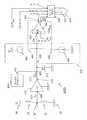
図3は、この発明の典型的な実施形態に従うメモリディバイス5の一部分を模式的な概観図で示す。図3に示される回路は、一つの基板の上に全部集積してもよい。抵抗性メモリセル(resistive memory cell)のクロスポイントアレイは、特定のメモリセルの抵抗をセンシング電圧により表わすことができるように構成されている。ディバイス5は、MRAMセル14のアレイ8、複数の一定間隔をおいた導電性の行ライン6、および複数の一定間隔をおいた導電性の列ライン12を含んでいる。複数の行ライン6は、複数の列ライン12に実質的に直角に配置され、それぞれの交差において複数の重複領域を定義する。他の実施形態では、行および列のラインは相互に傾斜して間隔をおいた関係で配置することができる。各行ラインは、それぞれのMRAM抵抗性セル14により、各列のラインに結合されている。一般的にはトランジスタで構成される複数のスイッチングディバイス51の各々が、行ライン6のそれぞれの一つ、第1の定電位源(source of constant potential)(グラウンド)20、および第2の定電位源(アレイ電圧Va)24に結合されている。制御回路61は行デコーダを含み、かつ点線62で示されるように、各スイッチングディバイス51と結合されている。スイッチングディバイス51は、制御回路61の制御の下に、行のライン6をグラウンド20および電圧源Va24と交互に接続するように構成されている。制御回路61は、各スイッチングディバイス51を、デフォルトで行ラインが接地された状態に維持する。スイッチングディバイス52は、読み出しサイクルの最中に行54が選択されたときのスイッチングディバイス51の状態を表わす。複数のセンシング回路50がそれぞれ列ライン12に接続されている。FIG. 3 shows a schematic overview of a portion of a memory device 5 according to an exemplary embodiment of the invention. The circuit shown in FIG. 3 may be entirely integrated on one substrate. A cross-point array of resistive memory cells is configured such that the resistance of a particular memory cell can be represented by a sensing voltage. The device 5 includes an array 8 of
電源装置(図示せず)は、この回路が動作する種々の電位を維持する電圧源を提供する。電源は、グラウンド電位20、回路要素に対する動作電圧Vcc、および上に記述されたように接続された電圧Va24を含む3つの電位を定義する。ある実施形態では、電圧Va24は約5Vである。A power supply (not shown) provides a voltage source that maintains the various potentials at which this circuit operates. The power supply defines three potentials includinga
図4には、選択されたスイッチングディバイス52により電圧Va24に結合された選択された行ライン54が示されている。複数の列ライン12のうち、特定のアドレスされた列ライン30が同様に示されている。選択された行ライン54と特定の列ライン30を接続するセンスされるメモリセル38の第1の端が、同様に示されている。それぞれのセンシング回路130は、グラウンド20に対する列ライン30の電圧をセンシングするために、列ライン30に動作的に接続されている。Shown in FIG. 4 is a selected
図示されているように、複数のメモリセル14の部分集合(サブセット:subset)を構成するスニークパスメモリセル(sneak path memory cell)、例えば、34、40、42、44、46が、列ライン30と複数の行ライン6のそれぞれとの間に接続されている。センスされるセル38に接続された一つを除いて、各行ライン6はそれぞれのスイッチングディバイス51により接地されている。このようにして、センスされる特定の抵抗セル38と直列に結合された、スニークパスのセル34、40、42、44、46の並列の組合せにより、分圧器が構成される。列ライン30は、スニークパスのセルとセンスされるセル38の間に、センシングノードを定義する。列ライン30におけるセンシング電圧は、センシング回路130に結合されている。 As shown, sneak path memory cells, eg, 34, 40, 42, 44, 46, that form a subset of the plurality of
ある実施形態では、選択された抵抗性メモリセル38の抵抗値は、約900kΩから約1.1MΩまでの範囲である。現在の技術を用いて用意された種々の実施形態においては、メモリセルの抵抗値は、低い抵抗状態では約900kΩから約1MΩまで、および高い抵抗状態では約950kΩから約1.1MΩまでの範囲に見いだされる。ある特定のディバイスにおいては、この低い範囲と高い範囲は重複しない。抵抗性セルの技術の進歩は、この発明がそれにもかかわらず効果的に適用される異なる抵抗値を生むかもしれないことが理解される。 In one embodiment, the resistance value of the selected
電圧、従ってそれによりメモリセルの論理状態をセンスするために、MRAMにおいて用いられるノイズシェイピングに基づくセンシング増幅器(noise shaping based sensing amplifier)は、固有のオフセットに帰着する。例えば、低い抵抗の状態ではセンス増幅器への入力電圧は1.992mVであり、高い抵抗の状態では入力電圧は2.212mVである。センスされるべき実際の信号は、これら二つの電圧間の差異すなわち約220μVである。センシング回路130は、データ(入力電圧)からオフセット、すなわち双方の入力電圧に共通な約2mVを、削減(減少)または除去する。 In order to sense the voltage and thus the logic state of the memory cell, the noise shaping based sensing amplifier used in the MRAM results in an inherent offset. For example, in the low resistance state, the input voltage to the sense amplifier is 1.992 mV, and in the high resistance state, the input voltage is 2.212 mV. The actual signal to be sensed is the difference between these two voltages, ie about 220 μV. The
このセンス増幅器のカウンタへの出力は一連のアップおよびダウンなので、オフセットの削減または除去により、アップおよびダウンの数をカウントするために用いられるカウンタのサイズを小さくすることができる。一般的にカウンタは、サンプリング期間中に起こりうる最大値および最小値をカウントするために、充分大きくなければならない。例えば、アップカウントはカウンタにおける1つ(+1)の値の増加に対応し、ダウンカウントはカウンタにおける1つ(−1)の値の減少に対応する。それで、111−11−1のシーケンスは、平均値(4−2)/6または1/3に対応する。オフセットの削減は、サンプリング期間中に発生する最大値の削減の効果を有し、それは、3つの1の初期の列の理由の故に、この例では3である。 Since the output to the sense amplifier counter is a series of ups and downs, the reduction or elimination of the offset can reduce the size of the counter used to count the number of ups and downs. In general, the counter must be large enough to count the maximum and minimum values that can occur during the sampling period. For example, an upcount corresponds to an increase of one (+1) value in the counter, and a downcount corresponds to a decrease of one (−1) value in the counter. Therefore, the sequence of 111-11-1 corresponds to the average value (4-2) / 6 or 1/3. The reduction in offset has the effect of reducing the maximum value that occurs during the sampling period, which is 3 in this example because of the three one initial column reasons.
サンプリング期間の終了時点で、カウント値がサンプリング期間中にVcapがVrefを超えた期間の比率(proportion)を示し、これは、Vinの測定値である。しかしながらこのカウント値は示された比率に等しい必要はない;例えば、オフセットは削減され、従ってゼロのカウント値が高い抵抗における比率を表わし、より高い零でないカウント値が低い抵抗における比率を表わす。At the end of the sampling period, the count value is the ratio of the period of Vcap during the sampling period exceeds Vref (proportion), which is a measure of Vin. However, this count value need not be equal to the indicated ratio; for example, the offset is reduced, so that a zero count value represents a ratio at high resistance, and a higher non-zero count value represents a ratio at low resistance.
このオフセットの補償は、センス増幅器で用いられるバイアス電流の調整により達成することができる。コンデンサが充電されている間に供給される正のバイアス電流は、放電期間中に供給される負のバイアス電流よりも低く設定することができる。典型的なセンス増幅器が適正に動作するためには、正および負のバイアス電流の平均は入力電流に等しくなければならない。即ち、ginVin=IupおよびIdownの平均値、である。This offset compensation can be achieved by adjusting the bias current used in the sense amplifier. The positive bias current supplied while the capacitor is being charged can be set lower than the negative bias current supplied during the discharge period. In order for a typical sense amplifier to operate properly, the average of the positive and negative bias currents must be equal to the input current. That is, gin Vin = an average value of Iup and Idown .
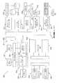
図5Aは、センシング回路400が抵抗性メモリディバイスの列ライン30に接続された入力410を有する、この発明の一実施形態である。センスされる抵抗性メモリセル38の一端は列ライン30に接続されている。列ライン30は同時に、抵抗39により表わされるスニークパスに接続されている。センシング回路400は、トランスコンダクタンス増幅器412を含んでいる。トランスコンダクタンス増幅器は、この増幅器の出力ノード416における電流414の出力が、増幅器の入力ノード418に印加される電圧Vinに比例するようにする、即ち、Iin=ginVinであるようにする、伝達関数ginを有している。増幅器の出力ノード416は、コンデンサ422の第1プレート420、クロック制御された比較器(clocked comparator)426の第1の入力424、電流源回路430のバイアスノード428および(オプションとして)アナログプリセット回路434の出力432に、それぞれ接続されている。アナログプリセット回路の機能は、別個のアナログプリセットを不要にするように適切に構成されたトランスコンダクタンス増幅器412により実行されてもよいことが留意されるべきである。FIG. 5A is an embodiment of the invention in which the
比較器426は2つの出力を有している。ここで、出力444は出力445の負(反対の論理状態)であることを表わすためのインバーターと共に示されている。これに代えて、出力445を出力444を得るために反転することができる。電流源430は、比較器426からの各スイッチのフィードバックに依存して開放または閉止される一組のスイッチ464、466の状態に従って、第1コンデンサプレート420からの電流を、交互に供給または引き出すために用いられる。双方のスイッチが同時に閉止されることはできない。クロック制御された比較器はさらに、基準電圧源440により基準電圧Vrefに維持されるように構成された第2の入力438、およびクロック信号CLKcmpを受取るように構成されたクロック入力442を含んでいる。比較器426の出力444、445はスイッチ464、466に結合されている。これらのスイッチは、電流源回路430のIup(正)電流およびIdown(負)電流の第1のコンデンサプレート420への結合を制御するトランジスタであってよい。スイッチ464は比較器426の出力444と結合され、スイッチ466は比較器426の出力445と結合されている。比較器の出力444、445はさらに、クロック制御されたカウンタ448のアップ/ダウン入力446、447にそれぞれ結合されている。クロック制御されたカウンタは、クロック入力450、プリセット入力452および複数のディジタル出力ライン456を含むディジタルカウント出力454を含んでいる。
動作においてプリセット電圧は、アナログプリセット回路434によりコンデンサ422に印加されている。ディジタルプリセット値は、ディジタルプリセット入力452に印加される信号遷移により、カウンタ448の出力454において設定されている。 In operation, the preset voltage is applied to the
コンデンサ422のプリセット電圧が、比較器426の第2の入力438に印加される基準電圧Vrefより小さいと仮定すると、比較器426のクロック入力442がクロック信号遷移を受取ると直ちに、比較器426の反転出力444はディジタルカウンタ448の入力446に対応するアップ入力を印加する。比較器の出力444、445はまた、電流供給回路430の双方のスイッチ464、466にそれぞれ印加される。従ってVcap<Vrefである間は、スイッチ464は閉止され、スイッチ466は開放されて、コンデンサ422への充電電流はIin+Iupになる。次にVcap>Vrefの場合、出力444および445がそれぞれスイッチ464を開放し、スイッチ466を閉止するので、コンデンサ422からの放電電流はIin−Idownになる。Assuming that the preset voltage of the
コンデンサ422の電圧は、比較器426の入力438に印加される基準電圧Vrefにより、定義された電圧閾値を超えて上昇する。その後コンデンサ422の電圧は、比較器426のクロック入力442においてクロックの遷移が検出されるまで上昇を続ける。クロック遷移の検出により、比較器426の出力444、445の論理状態は切り換わり(例えば、出力444の反転後に「0」から「1」へ、出力445において「1」から「0」へ)、対応するアップ入力をディジタルカウンタ448の入力446に印加する。それに応答して、電流供給回路430は、コンデンサ422からの電流の引き出しに、状態を変更する。電流がコンデンサ422から引き出されるので、コンデンサの電圧は下降し、やがて基準電圧Vref以下になる。その後、比較器426の入力442においてクロック信号が遷移すると、比較器の出力は再度切り換わるが、しかし今度はダウン信号が入力447に供給される。The voltage on the
カウンタ448は、そのプリセット値から周期的にカウントし、それに戻る。従ってこのカウンタは、交互の充電および放電期間中にアップおよびダウンをカウントして、ディジタルカウンタの時間平均値またはサンプリング期間の終了時点の値は、低い抵抗値についての高い値および高い抵抗値についての低い値の、2つの値のどちらか1つに接近しているべきである。 The
以上に記載したように、増幅器412からの電流414は、開放または閉止されたスイッチ464、466に従って、電流供給回路430からの電流460、462と加算される。電流供給回路430により供給されるバイアス電流なしでも、増幅器412からの電流414のセンスはコンデンサ422を充電しようとし、従ってコンデンサ422はそれが放電するよりもより早く充電される。それにより、コンデンサ422の電圧がVrefを超えるときのほうが、それがVref以下であるときよりも、比較器のクロック信号のより頻繁な上昇遷移が起こる。あるときには、コンデンサ422の電圧は、一クロック周期で生じる放電がコンデンサ422の電圧を基準電圧より下にするためには不十分な点まで上昇する。従って、コンデンサの電圧は、クロックの多数の連続した上昇遷移に対して、基準電圧より上である。As described above, the current 414 from the
電流源回路430は、ある電流値が供給されるように作成された2つの電流源460、462を有する。例えば電流源460、462は、固定電流を供給するように、常にオンであるように切り換えることができる。すなわち電流源460、462は、フォロワ(follower)のように常にオンである1つまたはそれ以上のトランジスタを含む回路として実現することができる。これに代えて、この回路は、あるトランジスタのゲート電圧の変化により電流を制御することが可能である回路として用いることができる。 The
Iup(正)電流の大きさがIdown(負)電流の大きさより下である電流源回路430を用いることは、サンプリング期間当たりのカウンタへのアップおよびダウン入力の数の平均値を削減し(減少させ)、従ってカウンタのサイズ(必要とされるビットの数)を削減することができる。これはカウンタにより良い全体としてのレンジを与える。Using a
Iup(正)およびIdown(負)電流の大きさを調整することにより、センス増幅器およびカウンタ双方の中心点を移動させることができる。適切に調整された場合には、カウンタ出力は最後にはほぼ零で終了する。即ち、Iup+ginVin≒Idownは、カウンタのセンタリングに帰着し、したがって、異なる抵抗値に対するアップ/ダウンがより小さい最大値および最小値を有し、従ってカウンタをより小さく作成することができる。By adjusting the magnitudes of the Iup (positive) and Idown (negative) currents, the center point of both the sense amplifier and the counter can be moved. If properly adjusted, the counter output will eventually end at approximately zero. That is, Iup + gin Vin ≈Idown results in counter centering, so up / down for different resistance values has smaller maximum and minimum values, thus making the counter smaller. it can.
図5Bは、センシング回路400における種々の信号の時間に対する動作の図を示す。双方の図において、時間は横軸に沿っている。上方の図では、実線は付加的なバイアス電流が印加されない場合のコンデンサ上の信号を示す。スイッチ464を経由したIup462により印加される正の電流(上方の図では点線で示されている)については、1つのクロックサイクルにおいて、コンデンサが閾値より下に放電することができないように時間にともなうコンデンサの充電を増加させる傾向があり、これは零より大きいカウント値を導く。しかしながら、正の電流よりさらに大きな量の負の電流を、スイッチ466を経由したIdown460(一点鎖線により示されている)により印加することができる。これは、カウンタを零に接近させる。カウンタの出力(下方の図で示されるような)は、時間t0で零のようなプリセット値から始まり、カウント値が実質的に一定であるように交番する。カウント値(+1)またはアップカウントにおける各増加に対して、対応する減少(−1)またはダウンカウントが存在する。最大のカウント値が+1であるので、より小さいカウンタを用いることができる。FIG. 5B shows a diagram of the operation of the
例えば、等しい量のIupおよびIdownを用いる場合の、論理零(0)または高い抵抗に対するカウンタ出力は156であり、論理1(1)または低い抵抗に対するカウンタ出力は180であることができる。等しくない量のIupおよびIdownを用いる場合の、論理零(0)に対するカウンタ出力は0であり、論理1(1)に対するカウンタ出力は24であることができる。9ビットカウンタが必要であるかもしれない場合に、6ビットカウンタで充分である − 顕著に小さいカウンタしか必要とされない。For example, when using equal amounts of Iup and Idown , the counter output for logic zero (0) or high resistance can be 156 and the counter output for logic one (1) or low resistance can be 180. When using unequal amounts of Iup and Idown , the counter output for logic zero (0) can be 0 and the counter output for logic 1 (1) can be 24. A 6-bit counter is sufficient if a 9-bit counter may be needed-only a significantly smaller counter is needed.
図6は、図5A−5Bに関連して上に開示されたこの発明のセンシング回路400を用いるメモリディバイス17を使用した典型的なディジタル処理システム500を示す。この処理システム500は、ローカルバス504と結合された一つまたはそれ以上のプロセッサ501を含んでいる。メモリコントローラ502および一次バスブリッジ503が、同様にローカルバス504に結合されている。処理システム500は、多数のメモリコントローラ502および/または多数の一次バスブリッジ503を含んでもよい。メモリコントローラ502および一次バスブリッジ503は、単一のディバイス506として集積してもよい。 FIG. 6 illustrates an exemplary
メモリコントローラ502はさらに、一つまたはそれ以上のメモリバス507と結合されている。各々のメモリバスは、センシング回路400を含む少なくとも一つのメモリディバイス17を含むメモリコンポーネント508を受け入れる。各メモリコンポーネント508は、メモリカードまたはメモリモジュールであってもよい。メモリモジュールの例は、シングルインラインメモリモジュール(SIMM)およびデュアルインラインメモリモジュール(DIMM)を含む。メモリコンポーネント508は、1つまたはそれ以上の追加的なディバイス509を含んでもよい。例えば、SIMMまたはDIMMにおいて、追加的なディバイス509は、シリアルプレゼンスデテクト(SPD)メモリのような、コンフィギュレーションメモリである。メモリコントローラ502はさらに、キャッシュメモリ505と結合されてもよい。このキャッシュメモリ505は、この処理システムにおける唯一のキャッシュメモリである。これに代えて、他のディバイス例えばプロセッサ501が、キャッシュメモリ505とキャッシュ階層を構成するキャッシュメモリを含んでもよい。処理システム500が、バスマスタであるかまたはダイレクトメモリアクセス(DMA)をサポートする周辺機器またはコントローラを含む場合には、メモリコントローラ502はキャッシュコヒーレンシープロトコルを実装していてもよい。メモリコントローラ502が複数のメモリバス507と結合されている場合には、各メモリバス507は並列に動作してもよく、または異なるアドレス範囲が異なるメモリバス507にマップされてもよい。
一次バスブリッジ503は、少なくとも一つの周辺バス510と結合されている。周辺バスブリッジまたは追加バスブリッジのような種々のディバイスが、周辺バス510と結合される。これらのディバイスは、ストレージコントローラ511、種々のI/Oディバイス514、二次バスブリッジ515、マルチメディアプロセッサ518、およびレガシーディバイスインターフェイス520を含んでもよい。一次バスブリッジ503はまた、1つまたはそれ以上の特別な目的の高速度ポート522と結合されてもよい。例えばパーソナルコンピュータでは、この特別な目的のポートはこの処理システム500に高性能ビデオカードを結合するために用いられるアクセラレーテッドグラフィックポート(AGP)であってもよい。
ストレージコントローラ511は、ストレージバス512を経由して1つまたはそれ以上のストレージディバイス513を周辺バス510と結合する。例えばストレージコントローラ511はSCSIコントローラであってよく、ストレージディバイス513はSCSIディスクであってよい。I/Oディバイス514は、任意の種類の周辺機器であってよい。例えばI/Oディバイス514は、イーサネットカードのようなローカルエリアネットワークインターフェイスであってよい。二次バスブリッジは、他のバスを経由して追加的なディバイスを処理システムにインターフェイスするために用いられてよい。例えば二次バスブリッジは、それを経由してUSBディバイス517を処理システム500に結合するために用いられるユニバーサルシリアルポート(USB)コントローラであってよい。マルチメディアプロセッサ518は、スピーカー519のような追加的な装置に結合されるサウンドカード、ビデオキャプチャカード、または他の種類のメディアインターフェイスであってよい。レガシーディバイスインターフェイス520は、例えば古い型式のキーボードおよびマウスであるレガシーディバイスを、処理システム500に結合するために用いられる。 The
図6に示される処理システム500は、この発明が用いられる処理システムの単なる例である。図6は、パーソナルコンピュータまたはワークステーションのような、汎用コンピュータに特に好適なプロセッシングアーキテクチャを示しているが、処理システム500が種々のアプリケーションにより好適に使用されるように構成するための周知の修正がなされうることを理解するべきである。例えば、処理を必要とする多くの電子ディバイスが、メモリコンポーネント508および/またはメモリディバイス100と結合されたCPU501に依拠する、より簡単なアーキテクチャを使用して実現されてもよい。これらの電子ディバイスは、限定する意図はないが、オーディオ/ビデオプロセッサおよびレコーダ、ゲーム機、ディジタルテレビ受像機、有線または無線の電話、ナビゲーション装置(グローバルポジショニングシステム(GPS)および/またはイナーシャルナビゲーションを含む)、およびディジタルカメラおよび/またはレコーダを含んでいる。修正または変形は例えば、不必要なコンポーネントの除去、特化されたディバイスまたは回路の追加、および/または複数のディバイスの集積を含んでいる。 The
この発明の実施形態が上に例示的に記述されているが、これらはこの発明の例であって、限定として考えられるべきものではないことが、理解されるべきである。この発明がMRAMについて記述されているが、それに限定されることはなく、例えば信号が異なるレベルでセンスされるPCRAMおよびその他の回路に対して適用可能である。追加、削除、置換およびその他の修正が、この発明の精神または範囲から逸脱することなくなされうる。従って、この発明は以上の記述により限定されるものとして考えられてはならず、添付された請求項の範囲によってのみ限定される。 While embodiments of the invention have been described above by way of example, it should be understood that these are examples of the invention and should not be considered as limiting. Although the present invention has been described for an MRAM, it is not so limited and is applicable, for example, to PCRAM and other circuits in which signals are sensed at different levels. Additions, deletions, substitutions, and other modifications can be made without departing from the spirit or scope of the invention. Accordingly, the invention should not be considered as limited by the foregoing description, but is only limited by the scope of the appended claims.
Claims (9)
Translated fromJapanese交番する充電期間と放電期間を含むサンプリング期間中に、該入力電流を受ける容量性素子;
該容量性素子の電圧が基準電圧を超えたか否かを示す周期的な比較信号を提供する比較回路;
該比較信号が該容量性素子の電圧が該基準電圧を超えたことを示すまで各充電期間中に正のバイアス電流を供給することにより、そして該比較信号が該容量性素子の電圧が該基準電圧を下廻ったことを示すまで、各放電期間中に、その大きさが該正のバイアス電流の大きさを超える負のバイアス電流を供給することにより周期的な比較信号に応答するバイアス電流回路;ならびに
該容量性素子の電圧が該基準電圧を超えたサンプリング期間の比率を示すカウント値を提供することにより、周期的な該比較信号に応答するカウント回路を備え、該カウント値が該入力電流の測定値である、
センシング回路。Input signal circuit for supplying input current;
A capacitive element that receives the input current during a sampling period including alternating charge and discharge periods;
A comparison circuit providing a periodic comparison signal indicating whether the voltage of the capacitive element exceeds a reference voltage;
Supplying a positive bias current during each charging period until the comparison signal indicates that the voltage on the capacitive element has exceeded the reference voltage, and the comparison signal causes the voltage on the capacitive element to until it shows that Shitamawa'voltage, during each dischargeperiod, the bias current circuitry responsive to a periodic comparison signalby the magnitude supplies a negative bias currentexceeding the magnitude of the bias current of thepositive;a rabbi voltage of <br/> said capacitive element by providing a count value indicating a ratio of a sampling period exceeds the reference voltage,comprising a counting circuit responsive to a periodic said comparisonsignal, the count The value is a measurement of the input current,
Se Nshingu circuit.
Applications Claiming Priority (2)
| Application Number | Priority Date | Filing Date | Title |
|---|---|---|---|
| US10/457,366US6795359B1 (en) | 2003-06-10 | 2003-06-10 | Methods and apparatus for measuring current as in sensing a memory cell |
| PCT/US2004/017885WO2004112049A1 (en) | 2003-06-10 | 2004-06-09 | Methods and apparatus for measuring current as in sensing a memory cell |
Publications (2)
| Publication Number | Publication Date |
|---|---|
| JP2007503680A JP2007503680A (en) | 2007-02-22 |
| JP4278687B2true JP4278687B2 (en) | 2009-06-17 |
Family
ID=32990951
Family Applications (1)
| Application Number | Title | Priority Date | Filing Date |
|---|---|---|---|
| JP2006533574AExpired - Fee RelatedJP4278687B2 (en) | 2003-06-10 | 2004-06-09 | Method and apparatus for current measurement, such as in memory cell sensing |
Country Status (8)
| Country | Link |
|---|---|
| US (2) | US6795359B1 (en) |
| EP (2) | EP1634301B1 (en) |
| JP (1) | JP4278687B2 (en) |
| KR (1) | KR100656066B1 (en) |
| CN (1) | CN100466108C (en) |
| AT (2) | ATE492884T1 (en) |
| DE (2) | DE602004018770D1 (en) |
| WO (1) | WO2004112049A1 (en) |
Families Citing this family (38)
| Publication number | Priority date | Publication date | Assignee | Title |
|---|---|---|---|---|
| US7006078B2 (en)* | 2002-05-07 | 2006-02-28 | Mcquint, Inc. | Apparatus and method for sensing the degree and touch strength of a human body on a sensor |
| US7046568B2 (en)* | 2002-09-24 | 2006-05-16 | Sandisk Corporation | Memory sensing circuit and method for low voltage operation |
| US6795359B1 (en)* | 2003-06-10 | 2004-09-21 | Micron Technology, Inc. | Methods and apparatus for measuring current as in sensing a memory cell |
| US7042783B2 (en)* | 2003-06-18 | 2006-05-09 | Hewlett-Packard Development Company, L.P. | Magnetic memory |
| US7123530B2 (en)* | 2003-10-09 | 2006-10-17 | Micron Technology, Inc. | AC sensing for a resistive memory |
| EP1881503A1 (en)* | 2006-07-21 | 2008-01-23 | Qimonda AG | Method and storage switching device for operating a resistance storage cell |
| US7428163B2 (en)* | 2006-07-21 | 2008-09-23 | Infineon Technologies Ag | Method and memory circuit for operating a resistive memory cell |
| US7397689B2 (en)* | 2006-08-09 | 2008-07-08 | Micron Technology, Inc. | Resistive memory device |
| CN101536106B (en) | 2006-11-08 | 2014-09-17 | Nxp股份有限公司 | Read enhancement for memory |
| US8054299B2 (en)* | 2007-01-08 | 2011-11-08 | Apple Inc. | Digital controller for a true multi-point touch surface useable in a computer system |
| US9135962B2 (en) | 2007-06-15 | 2015-09-15 | Micron Technology, Inc. | Comparators for delta-sigma modulators |
| US7830729B2 (en) | 2007-06-15 | 2010-11-09 | Micron Technology, Inc. | Digital filters with memory |
| US7969783B2 (en) | 2007-06-15 | 2011-06-28 | Micron Technology, Inc. | Memory with correlated resistance |
| US7817073B2 (en) | 2007-06-15 | 2010-10-19 | Micron Technology, Inc. | Integrators for delta-sigma modulators |
| US8117520B2 (en) | 2007-06-15 | 2012-02-14 | Micron Technology, Inc. | Error detection for multi-bit memory |
| US7538702B2 (en) | 2007-06-15 | 2009-05-26 | Micron Technology, Inc. | Quantizing circuits with variable parameters |
| US8068367B2 (en) | 2007-06-15 | 2011-11-29 | Micron Technology, Inc. | Reference current sources |
| US7733262B2 (en) | 2007-06-15 | 2010-06-08 | Micron Technology, Inc. | Quantizing circuits with variable reference signals |
| US7768868B2 (en) | 2007-06-15 | 2010-08-03 | Micron Technology, Inc. | Digital filters for semiconductor devices |
| US7667632B2 (en) | 2007-06-15 | 2010-02-23 | Micron Technology, Inc. | Quantizing circuits for semiconductor devices |
| US7818638B2 (en) | 2007-06-15 | 2010-10-19 | Micron Technology, Inc. | Systems and devices including memory with built-in self test and methods of making and using the same |
| US7839703B2 (en) | 2007-06-15 | 2010-11-23 | Micron Technology, Inc. | Subtraction circuits and digital-to-analog converters for semiconductor devices |
| CN101414819B (en)* | 2007-10-16 | 2010-09-08 | 通泰积体电路股份有限公司 | Current source control and compensation touch capacitive sensing method and device thereof |
| US7864609B2 (en) | 2008-06-30 | 2011-01-04 | Micron Technology, Inc. | Methods for determining resistance of phase change memory elements |
| US8581595B2 (en)* | 2008-08-15 | 2013-11-12 | Spansion Llc | Method of measuring flash memory cell current |
| KR101216393B1 (en)* | 2010-05-13 | 2012-12-28 | 주식회사 실리콘웍스 | Circuit and method for measuring capacitance value of touch screen |
| AT511664B1 (en)* | 2012-10-17 | 2016-01-15 | Avl List Gmbh | Digital charge amplifier |
| CN103871481B (en)* | 2012-12-12 | 2016-11-02 | 上海华虹宏力半导体制造有限公司 | Logic controller for non-volatility memorizer |
| US9330756B2 (en)* | 2014-08-13 | 2016-05-03 | Micron Technology, Inc. | Apparatuses and methods for sensing using an integration component |
| US9786346B2 (en)* | 2015-05-20 | 2017-10-10 | Micron Technology, Inc. | Virtual ground sensing circuitry and related devices, systems, and methods for crosspoint ferroelectric memory |
| US9589604B1 (en)* | 2015-09-17 | 2017-03-07 | International Business Machines Corporation | Single ended bitline current sense amplifier for SRAM applications |
| US9530513B1 (en) | 2015-11-25 | 2016-12-27 | Intel Corporation | Methods and apparatus to read memory cells based on clock pulse counts |
| KR102431206B1 (en)* | 2015-12-23 | 2022-08-11 | 에스케이하이닉스 주식회사 | Electronic device |
| US9508399B1 (en)* | 2016-05-03 | 2016-11-29 | HGST Netherlands B.V. | Residual capacitance performance booster |
| US9799381B1 (en)* | 2016-09-28 | 2017-10-24 | Intel Corporation | Double-polarity memory read |
| US10290327B2 (en)* | 2017-10-13 | 2019-05-14 | Nantero, Inc. | Devices and methods for accessing resistive change elements in resistive change element arrays |
| CN110890121B (en)* | 2018-09-07 | 2021-10-22 | 合肥沛睿微电子股份有限公司 | Storage device and NAND flash memory controller thereof |
| CN111351973B (en)* | 2018-12-20 | 2023-07-28 | Qorvo美国公司 | Current measuring circuit |
Family Cites Families (14)
| Publication number | Priority date | Publication date | Assignee | Title |
|---|---|---|---|---|
| FR2453471A1 (en)* | 1979-04-06 | 1980-10-31 | Inst Francais Du Petrole | IMPROVED SAMPLER-LOCKER |
| US4285051A (en)* | 1980-02-29 | 1981-08-18 | Precision Monolithics, Inc. | Low glitch current switch |
| US4783602A (en)* | 1987-06-26 | 1988-11-08 | American Telephone And Telegraph Company, At&T Bell Laboratories | Operational transconductance amplifier for use in sample-and-hold circuits and the like |
| DE3739208A1 (en)* | 1987-11-19 | 1989-06-01 | Siemens Ag | Analog/digital converter |
| FR2677771A1 (en)* | 1991-06-17 | 1992-12-18 | Samsung Electronics Co Ltd | Circuit for detecting the level of reverse bias in a semiconductor memory device |
| US5457035A (en)* | 1993-07-23 | 1995-10-10 | Immunex Corporation | Cytokine which is a ligand for OX40 |
| CN1202703A (en)* | 1997-06-17 | 1998-12-23 | 合泰半导体股份有限公司 | Sensing Circuit for Electrically Erasable Programmable Memory |
| US6160851A (en)* | 1998-02-26 | 2000-12-12 | National Semiconductor Corporation | Line driver calibration circuit |
| US6188615B1 (en)* | 1999-10-29 | 2001-02-13 | Hewlett-Packard Company | MRAM device including digital sense amplifiers |
| JP3985432B2 (en)* | 2000-06-19 | 2007-10-03 | 日本電気株式会社 | Magnetic random access memory |
| CN1385858A (en)* | 2001-05-10 | 2002-12-18 | 旺宏电子股份有限公司 | Non-Volatile Ferroelectric Memory Sensing Method |
| US6504750B1 (en)* | 2001-08-27 | 2003-01-07 | Micron Technology, Inc. | Resistive memory element sensing using averaging |
| US6597598B1 (en)* | 2002-04-30 | 2003-07-22 | Hewlett-Packard Development Company, L.P. | Resistive cross point memory arrays having a charge injection differential sense amplifier |
| US6795359B1 (en)* | 2003-06-10 | 2004-09-21 | Micron Technology, Inc. | Methods and apparatus for measuring current as in sensing a memory cell |
- 2003
- 2003-06-10USUS10/457,366patent/US6795359B1/ennot_activeExpired - Lifetime
- 2004
- 2004-06-09ATAT08167579Tpatent/ATE492884T1/ennot_activeIP Right Cessation
- 2004-06-09EPEP04754483Apatent/EP1634301B1/ennot_activeExpired - Lifetime
- 2004-06-09KRKR1020057023766Apatent/KR100656066B1/ennot_activeExpired - Fee Related
- 2004-06-09JPJP2006533574Apatent/JP4278687B2/ennot_activeExpired - Fee Related
- 2004-06-09EPEP08167579Apatent/EP2045817B1/ennot_activeExpired - Lifetime
- 2004-06-09WOPCT/US2004/017885patent/WO2004112049A1/enactiveApplication Filing
- 2004-06-09CNCNB2004800223470Apatent/CN100466108C/ennot_activeExpired - Fee Related
- 2004-06-09DEDE602004018770Tpatent/DE602004018770D1/ennot_activeExpired - Lifetime
- 2004-06-09DEDE602004030733Tpatent/DE602004030733D1/ennot_activeExpired - Lifetime
- 2004-06-09ATAT04754483Tpatent/ATE419626T1/ennot_activeIP Right Cessation
- 2004-07-29USUS10/901,183patent/US6930942B2/ennot_activeExpired - Lifetime
Also Published As
| Publication number | Publication date |
|---|---|
| EP1634301B1 (en) | 2008-12-31 |
| KR20060024408A (en) | 2006-03-16 |
| EP2045817A1 (en) | 2009-04-08 |
| WO2004112049A1 (en) | 2004-12-23 |
| EP1634301A1 (en) | 2006-03-15 |
| CN1833293A (en) | 2006-09-13 |
| US6930942B2 (en) | 2005-08-16 |
| KR100656066B1 (en) | 2006-12-11 |
| DE602004018770D1 (en) | 2009-02-12 |
| US20050002249A1 (en) | 2005-01-06 |
| EP2045817B1 (en) | 2010-12-22 |
| DE602004030733D1 (en) | 2011-02-03 |
| CN100466108C (en) | 2009-03-04 |
| ATE492884T1 (en) | 2011-01-15 |
| US6795359B1 (en) | 2004-09-21 |
| JP2007503680A (en) | 2007-02-22 |
| ATE419626T1 (en) | 2009-01-15 |
Similar Documents
| Publication | Publication Date | Title |
|---|---|---|
| JP4278687B2 (en) | Method and apparatus for current measurement, such as in memory cell sensing | |
| EP1717813B1 (en) | Dual loop sensing scheme for resistive memory elements | |
| KR101031028B1 (en) | How to reduce power consumption during resistive memory sensing | |
| US6259644B1 (en) | Equipotential sense methods for resistive cross point memory cell arrays | |
| US7489575B2 (en) | Noise resistant small signal sensing circuit for a memory device | |
| EP1126468B1 (en) | MRAM device including differential sense amplifiers | |
| US7263017B2 (en) | AC sensing for a resistive memory | |
| US20060013040A1 (en) | Adjusting the frequency of an oscillator for use in a resistive sense amp | |
| US7102913B2 (en) | Sensing scheme for programmable resistance memory using voltage coefficient characteristics |
Legal Events
| Date | Code | Title | Description |
|---|---|---|---|
| A521 | Request for written amendment filed | Free format text:JAPANESE INTERMEDIATE CODE: A821 Effective date:20060203 | |
| RD01 | Notification of change of attorney | Free format text:JAPANESE INTERMEDIATE CODE: A7426 Effective date:20060203 | |
| A621 | Written request for application examination | Free format text:JAPANESE INTERMEDIATE CODE: A621 Effective date:20060208 | |
| A977 | Report on retrieval | Free format text:JAPANESE INTERMEDIATE CODE: A971007 Effective date:20081209 | |
| A131 | Notification of reasons for refusal | Free format text:JAPANESE INTERMEDIATE CODE: A131 Effective date:20090120 | |
| A521 | Request for written amendment filed | Free format text:JAPANESE INTERMEDIATE CODE: A523 Effective date:20090121 | |
| TRDD | Decision of grant or rejection written | ||
| A01 | Written decision to grant a patent or to grant a registration (utility model) | Free format text:JAPANESE INTERMEDIATE CODE: A01 Effective date:20090225 | |
| A01 | Written decision to grant a patent or to grant a registration (utility model) | Free format text:JAPANESE INTERMEDIATE CODE: A01 | |
| A61 | First payment of annual fees (during grant procedure) | Free format text:JAPANESE INTERMEDIATE CODE: A61 Effective date:20090310 | |
| FPAY | Renewal fee payment (event date is renewal date of database) | Free format text:PAYMENT UNTIL: 20120319 Year of fee payment:3 | |
| R150 | Certificate of patent or registration of utility model | Ref document number:4278687 Country of ref document:JP Free format text:JAPANESE INTERMEDIATE CODE: R150 Free format text:JAPANESE INTERMEDIATE CODE: R150 | |
| FPAY | Renewal fee payment (event date is renewal date of database) | Free format text:PAYMENT UNTIL: 20120319 Year of fee payment:3 | |
| FPAY | Renewal fee payment (event date is renewal date of database) | Free format text:PAYMENT UNTIL: 20130319 Year of fee payment:4 | |
| R250 | Receipt of annual fees | Free format text:JAPANESE INTERMEDIATE CODE: R250 | |
| FPAY | Renewal fee payment (event date is renewal date of database) | Free format text:PAYMENT UNTIL: 20130319 Year of fee payment:4 | |
| FPAY | Renewal fee payment (event date is renewal date of database) | Free format text:PAYMENT UNTIL: 20140319 Year of fee payment:5 | |
| R250 | Receipt of annual fees | Free format text:JAPANESE INTERMEDIATE CODE: R250 | |
| R250 | Receipt of annual fees | Free format text:JAPANESE INTERMEDIATE CODE: R250 | |
| R250 | Receipt of annual fees | Free format text:JAPANESE INTERMEDIATE CODE: R250 | |
| R250 | Receipt of annual fees | Free format text:JAPANESE INTERMEDIATE CODE: R250 | |
| R250 | Receipt of annual fees | Free format text:JAPANESE INTERMEDIATE CODE: R250 | |
| R250 | Receipt of annual fees | Free format text:JAPANESE INTERMEDIATE CODE: R250 | |
| R250 | Receipt of annual fees | Free format text:JAPANESE INTERMEDIATE CODE: R250 | |
| R250 | Receipt of annual fees | Free format text:JAPANESE INTERMEDIATE CODE: R250 | |
| R250 | Receipt of annual fees | Free format text:JAPANESE INTERMEDIATE CODE: R250 | |
| R250 | Receipt of annual fees | Free format text:JAPANESE INTERMEDIATE CODE: R250 | |
| LAPS | Cancellation because of no payment of annual fees |