JP4276891B2 - Microchannel and microchemical chip including the same - Google Patents
Microchannel and microchemical chip including the sameDownload PDFInfo
- Publication number
- JP4276891B2 JP4276891B2JP2003137915AJP2003137915AJP4276891B2JP 4276891 B2JP4276891 B2JP 4276891B2JP 2003137915 AJP2003137915 AJP 2003137915AJP 2003137915 AJP2003137915 AJP 2003137915AJP 4276891 B2JP4276891 B2JP 4276891B2
- Authority
- JP
- Japan
- Prior art keywords
- wall member
- fine
- planar
- fine channel
- flow path
- Prior art date
- Legal status (The legal status is an assumption and is not a legal conclusion. Google has not performed a legal analysis and makes no representation as to the accuracy of the status listed.)
- Expired - Fee Related
Links
Images


Landscapes
- Investigating Or Analysing Materials By Optical Means (AREA)
- Micromachines (AREA)
- Physical Or Chemical Processes And Apparatus (AREA)
- Optical Measuring Cells (AREA)
- Automatic Analysis And Handling Materials Therefor (AREA)
Description
Translated fromJapanese【0001】
【産業上の利用分野】
本発明は、微細流路およびこれを含むマイクロ化学チップならびにこれらの製造方法に関するものである。
【0002】
【従来の技術】
光学的な分析のための幅100μm、深さ50μm程度の微細な溝や、直径数百μmの窪み等を含む流路を一辺が数十mmのガラス基板上に集積したマイクロ化学チップは、フロー状態で微量な化学物質の反応や合成および抽出を行なったり、様々な長さに切断されたDNA断片を分離したりするために用いられている。DNA分析に用いられるものは、DNAチップと称される。
【0003】
このマイクロ化学チップを用いた分析は、ガラス基板上に設けられた上述した溝を電気泳動等により流れる流体あるいは窪みに蓄積された化学物質を分析対象とし、これら微小な溝あるいは窪みに紫外光や赤外光を照射して、その部分からの反射光、透過光を光学素子を通して分析部に導くことにより行われる。
【0004】
このような用途に用いられる微細流路は、開口断面の代表寸法が数十μm〜数百μmの微細配管となっている。
【0005】
図1にDMA断片の分離等に用いられる微細直管流路(キャピラリ)電気泳動装置としてのマイクロ化学チップの一例を示す。また、図2は微細流路2の断面図、図3はマイクロ化学チップの外観図である。
【0006】
透明絶縁基板1上には十字形に交差する直線状の2本の微細流路である定量用流路2および検出用流路3が凹設され、これらの微細流路2,3はその上に封入用透明絶縁板4を重ねて接着剤等で密着固定することにより封止されている。この封入用透明絶縁板4にはサンプルを注入・抽出するための開口部5が微細流路に対応して設けられている。また封入用透明絶縁基板4には各微細流路の両端部に電極が設けられている。さらに、微細流路の内部にはナノメートルスケールの網目構造を持つゲルが封入されている。
【0007】
ここで、流路では後述するように光学的な分析が行われるため、透明絶縁基板としては光学特性に優れた石英を使用することが多い。そして、流路は、通常はエッチング加工で溝を掘ることにより形成しているため、図2の断面図に示すように、略半円状の断面形状を有している(非特許文献1参照)。
【0008】
また、図3は完成したマイクロ化学チップ10の外観および内部状態を示す透視図であって、微細流路に対する注入口および電極6が形成された例を示している。
【0009】
次に、このようなマイクロ化学チップの使用法につき説明する。微細流路の両端に設けられた電極の一方を接地電位とし、他方に正の所定電圧を印加すると、マイナスに帯電しているサンプル(DNA等)がプラス電極側に移動する電気泳動現象が起こる。この例では、サンプルは緩衝液と共に定量用流路の接地側からプラス電極側に流され、交差点でこの部分の容積に相当する量だけ蓄積され、続いて検出用流路をプラス側に向かって流れる。この時、DNAはその長さによって帯電量が異なり、また封止されたゲルの網目構造との相互作用も異なるため、長さが短いものほど速く進む。したがって、DNAの長さにより流路上の位置が異なることにより分離を行うことが可能となる。
【0010】
このようにして分離されたDNAは紫外線吸収を利用し、あるいはDNAに蛍光修飾させてその光量測定を行うことにより観測することができる。
【0011】
図4は、マイクロ化学チップの機能をまとめた模式図である。この図には、二つの薬品A、Bを混合させて流路上で反応させたり、流路上で分離を行ったり、流路上の物質を光透過により検出することが可能であることを示している。
【0012】
【非特許文献】
「マイクロマシニング技術を用いた石英製電気泳動チップの作製とその基本特性評価」中西博昭他、島津評論vol.56 No.1-2, 1999.8
【0013】
【発明が解決しようとする課題】
しかしながら、透明基板材料としての石英は非常にエッチングされにくい物質であるため、加工がきわめて困難であり、エッチングレートは条件によっては1分間に1μm以下の少量となってしまい、量産は困難であった。また、DNA等を抽入する挿入口も一般的には平面的な基板部材に開口部とコネクタを取り付ける方式が採用されており、このような構造も加工性と量産性を妨げている。
【0014】
また、これらの微細流路による生成物を電子的に計測するため、機能性薄膜やチップ状のシリコン回路などの計測補助手段をこの微細流路近傍に配設する場合があるが、従来は、これらの計測手段とこれに付随する要素や部品を、流路の上面あるいは下面に配設するのが一般的で、微小流路の周囲部位が最適かつ効率的に使用されているとは言い難かった。
【0015】
さらに、微細流路の使用法として、単に計測を行うのみでなく微細流路周囲の物理環境を調整する場合がある。例えば、微細流路周囲の温度を上昇させるためのヒータ、あるいは温度下降させるための冷媒管を微細流路に隣接して設ける場合があるが、これらの物理環境調整機器も従来は流路の上下にしか配設されていない。
【0016】
また、微細流路をプレス成形で造る場合(特願昭2002−89495b号参照)、金型としてしては流路のネガとなる凸状部分を有することが必要となるが、これを作るためには広い面積にわたって機械的あるいはエッチングにより削り込まねばならない。プレス成形では金型の表面が素材に正確に転写されるので、精度を確保するにはかなりの時間をかけて加工を行う必要がある。
【0017】
本発明は加工性と量産性に優れ、計測補助手段や物理環境調整機器を周囲に配置することのできる微細流路およびこれを有するマイクロ化学チップを提供することを目的とするものである。
【0018】
【課題を解決するための手段】
本発明の実施形態によれば、一表面に微細流路幅を隔てて対をなす壁部材が凸状に形成された透光性のガラスあるいはシリコン材料で構成された第1の平面部材と、少なくとも前記壁部材の頂部と接するように取り付けられた透光性のガラスあるいはシリコン材料で構成された2の平面部材とを備え、前記第1の平面部材表面と、前記壁部材と前記第2の平面部材で囲まれる閉空間により形成された微細流路において、前記突状に形成された壁部材は三角形状あるいは略台形状の断面形状を有しており、その側辺の少なくとも一方に光反射膜が形成されたことを特徴とする。
【0021】
本発明の実施形態によれば、一表面に微細流路幅を隔てて対をなす壁部材が凸状に形成された透光性のガラスあるいはシリコン材料で構成された第1の平面部材と、少なくとも前記壁部材の頂部と接するように取り付けられた透光性のガラスあるいはシリコン材料で構成された2の平面部材とを備え、前記第1の平面部材表面と、前記壁部材と前記第2の平面部材で囲まれる閉空間により形成された複数の微細流路と、前記複数の微細流路への注入、取り出し用のウェルと、前記微細流路の途中に設けられた、分析のための光学素子と、を備えたマイクロ化学チップにおいて、前記壁部材は三角形状あるいは略台形状の断面形状を有しており、その側辺の少なくとも一方に光反射膜が形成されたことを特徴とする。
【0022】
【発明の実施の形態】
以下、本発明の実施の形態のいくつかを図面を参照しながら説明する。
【0023】
図5は本発明に係る微細流路の第一の実施形態を示す断面図であり、マイクロ化学チップに使用される。
【0024】
平面基板101上には断面が略台形あるいは略三角形状の壁部材101a、101bが流路幅分離隔して凸設されており、これら壁部材の上には第2の平面基板102が載せられ、これにより閉じた空間が流路103を形成している。この第2の平面基板102と壁材101a、101bとの間には接着層105が介在し、これらの部材を締結している。
【0025】
壁材101a、101bの流路103よりも外側の空間104a、104bは接着強度が十分ならば中空のままで良く、ここに流路内の観測要素部品や環境調整部品を装着することができる。また、接着強度が十分でない場合には、熱硬化性樹脂などの充填剤を注入して硬化させることができる。
【0026】
なお、流路は概略紙面手前から奥に向かっているものとし、流路の両端部には電極および注入口/取出口(図示せず)が設けられている。本微細流路は基本的に流れの方向に開口される構造なので、素材に応じた接合手段や連接手段により流路の延長や、異なる機能の流路との組み合わせが容易にできる。
【0027】
図6は本発明に係る微細流路の第2の実施形態を示す断面図であり、流路の方向や電極および注入口/取出口(図示せず)の位置については全く同様の構成となっていてる。
【0028】
この実施の形態では、略台形あるいは略三角形状の壁部材111aを有する第1の平面基板111と、略台形あるいは略三角形状の壁部材112aを有する第1の平面基板112とを互いに反転した状態で対向させ、これにより形成された閉空間113を微細流路として用いるものである。第1の実施の形態と同様に、壁部材とそれに接する平面基板間には接着層115が介在して締結を行っている。
【0029】
この実施の形態でも壁材111a、112aの流路103よりも外側の空間114a、114bは接着強度に応じ、中空のままでも、熱硬化性樹脂やガラスなどの充填剤を注入して硬化させても良い。
【0030】
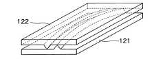
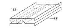
この実施の形態で特徴的なのは、部品点数を減少できることと、微細流路の幅を自由に調整できることである。すなわち、2つの壁部材111aと111bとの距離は自在に調整できるため、用途に応じた微細流路幅を選択できる。なお、壁部材は直線状の形状とは限らず、図7に示す曲線状の壁部材を有する平面基板121、122、図8に示すジグザグ状の壁部材を有する平面基板131、132等種々の形状のものを採用することができる。
【0031】
図9は第3の実施の形態を説明するもので、断面三角形状の壁部材が2つ平行に配置された平面基板141と142を互いに反転して組み合わせたものである。この場合、対向する平面基板の壁部材の角度を壁全体が接触するような角度とし、この接触面に接着剤143を塗布して固着するようにしている。この実施の形態では壁部材の角度は水平に対して60°の角度をなしており、この結果、接着面積を大きく取れるので空間部に充填材を注入しなくても、強度的な確保が可能となっている。
【0032】
図10は上述した壁部材を有する平面基板を成形により作製する方法を示す模式図である。ここでは上金型301と下金型302との間に石英材料303を挟んでブレスを行っている様子を示している。
【0033】
このようにマイクロ化学チップ等の微細流路では耐薬品性や光学特性の点から石英が用いられる。しかし、石英の場合、真空・高温での加工環境を要求されるため、金属性の金型の適用は難しく、ガラス状カーボンが好適な材料として使用されることが多い。しかしながら、この素材は加工が困難であり、現状では溝をの掘る加工をかろうじて行える程度である。本願発明では、各平面基板はこの溝加工された金型を用いて凸状の壁部材を有する平面基板を得ている。したがって、金型素材を大面積平面で研削やエッチングをする必要がないので、量産が可能であり、製造コストを下げることができる。例えば、石英に深さ100μm程度の溝を形成する場合、これまでは数時間の加工時間を要していたが、本発明の構成によれば数分で微細流路の形成が終了する。
【0034】
なお、壁部材の形状を工夫すれば、第一及び第二の実施の形態のいずれでも交差流路を形成することができる。また、注入部分、取り出し部分のウェルも平面基板の追加加工を行うことにより容易に形成することができる。
【0035】
以下、微細流路の近傍の空間に種々の機能を持たせた実施の形態を説明する。
【0036】
前述した本発明の実施形態にかかる微細流路は、流れ方向以外の方向は薄肉状の壁で囲まれた構成となっているため、そこに種々の部材、部品、素子等を配置することが可能になる。例えば、流路内の状況を観測するセンサや、熱や電磁気など物理的な環境を変化させる要素部品を配設することができる。また、光学的な取り扱いをする場合、壁材の一部を光学部品状に成形して利用される。さらに、シリコン部材上に構築されたセンサ等を用いる場合には、この部材自体が流路を構成する壁面に利用される。
【0037】
流路の連結や試薬サンプルの抽入は、本発明の微細流路の構造上、流れの断面方向に関連する部材等が装着される。
【0038】
以下、代表的なものを詳述する。
【0039】
図11は微細流路の壁部材を反射光学系に利用した実施の形態を示す断面図である。
【0040】
この実施の形態では、平面基板151の微細流路153を構成する壁部材151a、151bの表面に反射膜154a、154bを形成し、上部基板152上にはLED等の発光部155とPD等の受光部156を平面部材の屈折率を配慮して配設し、微細流路を横切るような光路157を構築した。
【0041】
このような構成により、微細流路流体の速度計測や分光計測が可能となる。
【0042】
図12は図11と同様に、微細流路の壁部材を反射光学系に利用した実施の形態を示す断面図である。この実施の形態では発光部165と受光部166を平面基板161の下部に配置している点が異なる。すなわち、壁部材161a、161bの内部反射と屈折を利用して光路を構築している点に特徴がある。
【0043】
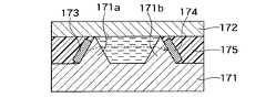
図13は壁部材の外側の領域を有効に使用した実施の形態を示しており、壁部材171a、171b面に直接発光部173および受光部174を配設したものである。このような発光部173および受光部174を配設するには、壁部材表面に直接成膜処理を施しても良く、また、上下平面基板間の空間に後から組み立てても良い。この空間内に後に充填される材料175が発光部173、受光部174に対するモールド材としても兼用される。
【0044】
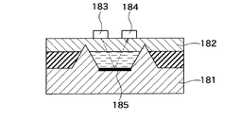
図14は平面部材の一方をシリコン基板とした実施の形態を示す断面図である。すなわち、第1の平面基板181はこれまでの各実施の形態の場合と同様の構成を有しているが、その上に重ねられる第2の平面基板182はシリコン基板となっている。このシリコン基板182の上には各種センサデバイスや処理用の電子回路をこの上に直接形成することが可能となる。図14に示した例では発光部183と受光部184をシリコン基板182上に形成している。
【0045】
また、この実施の形態では流路底面に反射膜185を設け、発光部183から発光された光が流路を通って底面の反射膜185で反射して受光部184に達する光路を形成している。また、壁部材の頂角θをシリコン結晶をエッチングする際に特異的に規定される角度より狭く設定することにより、位置決めの容易性も達成できる。
【0046】
なお、シリコン以外の材料を平面基板として用いることもできるが、その場合には、素材に応じて位置決め用の溝加工や頂角θの設定をすれば良い。
【0047】
以上は光学デバイスを例に示したが、温度デバイスや、電磁気的なデバイスであっても、特性に応じた成膜を流路近傍の領域に形成することができる。以下、そのような実施の形態について説明する。
【0048】
図15は微細流路内の温度制御を行うことを可能とした実施の形態を説明する断面図である。
【0049】
この実施の形態では、第1の平面基板191に設けられた壁部材191a、101bの内壁に、第2の平面基板192に設けられた壁部材192a、192bの外壁が嵌り合う寸法関係になっており、これらの組み合わせで流路が形成されている。
【0050】
一方、第1の平面基板191の下面には冷却源194が、第2の平面基板192の上面には加熱源193が設けられている。これらの加熱・冷却源は必要に応じて流路に沿って配設される。加熱源としては通常のヒータ、ホットエアなど、冷却源として水冷パイプなど各種のものを使用することができるが、適正な寸法に形成したレーザや赤外線を用いると加熱時のみその熱源の寸法に応じた領域で温度を上昇させることができる。図中の矢印は加熱源からの熱の移動を示す。また、同様に冷却源としてペルチェ素子、ヒートシンクやファンを用いることにより、加熱停止時に冷却源によって温度を下降させることができる。
【0051】
また、流路直上の第2の平面基板上には、温度計測手段195が取り付けられ、図示されない制御機器を用いて温度制御を行うことが可能となる。
【0052】
図16も、加熱冷却を行うようにしてなる実施の形態を示しており、第1の平面基板201と、その上に第2の平面基板が搭載されている点ではこれまでの例と同じであるが、これらを貫通するように、微細流路近傍に加熱管203と冷却管204を設けた点が異なる。
【0053】
また、流路直上の第2の平面基板202上に温度制御要素が設けられており、その計測結果に基いてこれらの管に熱媒体を供給し、あるいは冷媒を供給することにより、流路領域の温度を制御することができる。
【0054】
これらの熱源と冷却源、並びに温度計測手段および微細流路の形状は、目的に応じて任意に組み合わせることが可能である。また、温度制御範囲も任意に選択することができる。なお、図16に示すような構成で、温度だけでなく電磁気や光学的な線源を利用する場合も同様な配設手法が可能である。
【0055】
図17は、さらに別の実施の形態を示す断面図である。上述した各実施の形態では平面基板はガラス板等の緻密な材料であったが、この実施の形態では、断面が略三角形の流路が並設されるように溝が形成された第1の平面基板211の上部に取り付けられるのは多孔質の基板212である。そしてこの多孔質基板212の上には機能性物質膜213が形成されている。この機能性物質膜は選択的なものである。また、第1の平面基板212の下面には熱源215がもうけられている。
【0056】
このような流路では、流路内に多孔質部材の孔径より小さい物質が存在する場合、この物質は選択的に透過して参照番号214で示されるように外部に流出する。この結果、流路内外で圧力差が生じ、この圧力差は流路内の通過物質を圧力源で加圧し、あるいは熱源215で加熱して流路内物質に熱エネルギーを付与することにより増大される。また、レーザ照射や物質の反応エネルギーを利用することもできる。
【0057】
多孔質基板の表面、或いは孔の内部に付加される機能性物質としては物質の選択性を高める機能を有する膜等が使用される。これは、一般に多孔質基板における物質の透過は、温度が高い方が良好であるが、流路側および封止側基板の熱膨張係数を近づけておくために、例えば流路側基板に石英を使用する時、封止側には高珪酸成分ガラスを用い、機能性物質としてRhやシリカゾルを焼結したものを用いれば、水素を選択的にさせる事が可能となる。
【0058】
以上の各実施の形態では、基板は略平面であり、壁状部材はその断面が三角形あるいは台形等の矩形としてあるが、加工が可能であればこれに限るものではない。例えば基板には起伏があっても良いし、形勢される微細流路は同一の深さや高さである必要はない。
【0059】
【発明の効果】
以上のように、本発明の実施の形態によれば、微細流路は、プレス成形された部品を組み立てる事で構築されるため、金型加工が容易で量産性に優れる。
【0060】
また、微細流路は流路を構成する壁部材の外方に多くの空隙があるため、この空隙に種々の機能部品等を配置でき、有用性を高めることができる。
【0061】
さらに、微細流路をそれぞれ壁部材となる凸状部分を有する2つの平面基板を対向配置することにより形成するものでは、従来不可能であった、流路幅の調整が可能となる。
【図面の簡単な説明】
【図1】従来のマイクロ化学チップの構成を説明する斜視図である。
【図2】従来のマイクロ化学チップにおいて使用される溝を説明する断面図。
【図3】マイクロ化学チップ完成品の外観を示す斜視図。
【図4】マイクロ化学チップの機能の説明図である。
【図5】本発明の実施の形態による微細流路の形成を示す断面図である。
【図6】−本発明の他の実施の形態による微細流路の形成を示す断面図である。
【図7】曲線状に形成された微細量路を示す説明図である。
【図8】屈曲状に形成された微細量路を示す説明図である。
【図9】壁部材の側面に接着層を設け流路を形成した実施の形態を示す断面図である。
【図10】微細流路を構成する壁部材を含む基板を金型で成形する様子を示す断面図である。
【図11】微細流路の壁部材を反射光学系に利用した実施の形態を示す断面図である。
【図12】平面基板に発光部と受光部を設けた実施の形態を示す断面図である。
【図13】壁部材に発光部と受光部を設けた実施の形態を示す断面図である。
【図14】平面部材の一方をシリコン基板とした実施の形態を示す断面図である。
【図15】微細流路内の温度制御を行うために加熱源を設けた実施の形態を説明する断面図である。
【図16】微細流の近傍に加熱・冷却管を配設した実施の形態を示す断面図である。
【図17】多孔質部材を含む実施形態を示す断面図である。
【符号の説明】
111、112、121、122、131、132、141、142、151、181、182、191、211 平面基板
111a、112a、151a、151b、161a、161b、171a、171b、191a、192b 壁部材
115 接着層
301 上金型
302 下金型
153 微細流路
154a、154b、185 反射膜
152 上部基板
155、165、173、183、184 発光部
156、166、174 受光部
193 加熱源
194 冷却源
212 多孔質の基板
213 機能性物質膜[0001]
[Industrial application fields]
The present invention relates to a microchannel, a microchemical chip including the microchannel, and a method for producing the same.
[0002]
[Prior art]
A microchemical chip in which a flow path including a fine groove having a width of about 100 μm and a depth of about 50 μm for optical analysis and a recess having a diameter of several hundred μm is integrated on a glass substrate having a side of several tens of millimeters is a flow It is used for the reaction, synthesis and extraction of trace amounts of chemical substances in the state, and for separating DNA fragments cut into various lengths. Those used for DNA analysis are called DNA chips.
[0003]
The analysis using this microchemical chip is intended to analyze the fluid flowing by electrophoresis or the like in the groove provided on the glass substrate or the chemical substance accumulated in the depression, and ultraviolet light or It is performed by irradiating infrared light and guiding reflected light and transmitted light from the portion to the analysis section through the optical element.
[0004]
The fine flow path used for such an application is a fine pipe having a typical dimension of an opening cross section of several tens to several hundreds of micrometers.
[0005]
FIG. 1 shows an example of a microchemical chip as a micro straight channel (capillary) electrophoresis apparatus used for separating DMA fragments and the like. 2 is a cross-sectional view of the
[0006]
On the transparent insulating substrate 1, two linear flow channels that intersect in a cross shape, that is, a
[0007]
Here, since optical analysis is performed in the flow path as described later, quartz having excellent optical characteristics is often used as the transparent insulating substrate. And since the flow path is normally formed by digging a groove by etching, it has a substantially semicircular cross-sectional shape as shown in the cross-sectional view of FIG. 2 (see Non-Patent Document 1). ).
[0008]
FIG. 3 is a perspective view showing the appearance and internal state of the completed
[0009]
Next, how to use such a microchemical chip will be described. When one of the electrodes provided at both ends of the microchannel is set to the ground potential and a predetermined positive voltage is applied to the other, an electrophoretic phenomenon occurs in which a negatively charged sample (DNA or the like) moves to the positive electrode side. . In this example, the sample is flowed together with the buffer from the ground side to the plus electrode side of the quantification channel, and is accumulated by an amount corresponding to the volume of this portion at the intersection, and then the detection channel is moved toward the plus side. Flowing. At this time, the amount of charge of DNA differs depending on its length, and the interaction with the network structure of the sealed gel also differs, so that the shorter the length, the faster the DNA. Therefore, the separation can be performed by changing the position on the flow path depending on the length of the DNA.
[0010]
The DNA thus separated can be observed by utilizing ultraviolet absorption, or by fluorescently modifying the DNA and measuring the amount of light.
[0011]
FIG. 4 is a schematic view summarizing the functions of the microchemical chip. This figure shows that two chemicals A and B can be mixed and reacted on the flow channel, separated on the flow channel, and substances on the flow channel can be detected by light transmission. .
[0012]
[Non-patent literature]
“Manufacture of quartz electrophoresis chip using micromachining technology and evaluation of its basic characteristics” Hiroaki Nakanishi et al., Shimazu review vol.56 No.1-2, 1999.8
[0013]
[Problems to be solved by the invention]
However, since quartz as a transparent substrate material is a substance that is very difficult to etch, it is extremely difficult to process, and the etching rate is a small amount of 1 μm or less per minute depending on conditions, making mass production difficult. . In addition, a method of attaching an opening and a connector to a planar substrate member is generally employed for an insertion port for drawing DNA or the like, and such a structure also hinders workability and mass productivity.
[0014]
In addition, in order to electronically measure the products by these fine channels, measurement auxiliary means such as a functional thin film or a chip-like silicon circuit may be disposed in the vicinity of the fine channels. These measuring means and their associated elements and parts are generally arranged on the upper or lower surface of the flow path, and it is difficult to say that the area around the micro flow path is used optimally and efficiently. It was.
[0015]
Furthermore, as a method of using the fine flow path, there are cases where the physical environment around the fine flow path is adjusted in addition to simply measuring. For example, a heater for raising the temperature around the fine flow path or a refrigerant pipe for lowering the temperature may be provided adjacent to the fine flow path. It is arranged only in.
[0016]
Further, in the case where the fine flow path is manufactured by press molding (see Japanese Patent Application No. 2002-89495b), it is necessary for the mold to have a convex portion that becomes the negative of the flow path. In this case, it must be machined or etched over a large area. In press molding, since the surface of the mold is accurately transferred to the material, it is necessary to perform processing for a considerable time to ensure accuracy.
[0017]
SUMMARY OF THE INVENTION An object of the present invention is to provide a fine flow channel that is excellent in processability and mass productivity and in which a measurement auxiliary means and a physical environment adjusting device can be arranged around, and a microchemical chip having the same.
[0018]
[Means for Solving the Problems]
According to an embodiment of the present invention, a first planar member made of translucent glass orsilicon material in which a wall member forming a pair with a fine channel width on one surface is formed in a convex shape; Two planar members made of translucent glass orsilicon material attached so as to be in contact with at least the top of the wall member, the surface of the first planar member, the wall member, and the second member In the fine flow path formed by the closed space surrounded by the planar member, theprotruding wall member has a triangular or substantially trapezoidal cross-sectional shape, and reflects light on at least one of its side edges. A film is formed .
[0021]
According to an embodiment of the present invention, a first planar member made of translucent glass orsilicon material in which a wall member forming a pair with a fine channel width on one surface is formed in a convex shape; Two planar members made of translucent glass orsilicon material attached so as to be in contact with at least the top of the wall member, the surface of the first planar member, the wall member, and the second member A plurality of microchannels formed by a closed space surrounded by a planar member, wellsfor injection and extraction into the plurality of microchannels, and an optical for analysis provided in the middle of the microchannels Thewall member has a triangular or substantially trapezoidal cross-sectional shape, and a light reflecting film is formed on at least one side of the wall member.
[0022]
DETAILED DESCRIPTION OF THE INVENTION
Hereinafter, some embodiments of the present invention will be described with reference to the drawings.
[0023]
FIG. 5 is a cross-sectional view showing a first embodiment of a microchannel according to the present invention, which is used for a microchemical chip.
[0024]
On the
[0025]
The
[0026]
It is assumed that the flow path is substantially from the front side of the paper to the back, and electrodes and inlet / outlet ports (not shown) are provided at both ends of the flow path. Since this fine channel basically has a structure that opens in the direction of flow, the channel can be easily extended or combined with channels having different functions by means of joining or connecting according to the material.
[0027]
FIG. 6 is a cross-sectional view showing a second embodiment of the fine channel according to the present invention, and the configuration of the channel and the positions of the electrodes and the inlet / outlet (not shown) are exactly the same. I am.
[0028]
In this embodiment, the first
[0029]
Also in this embodiment, the
[0030]
What is characteristic in this embodiment is that the number of parts can be reduced and the width of the fine channel can be freely adjusted. That is, since the distance between the two
[0031]
FIG. 9 illustrates a third embodiment, in which
[0032]
FIG. 10 is a schematic view showing a method for producing a planar substrate having the above-described wall member by molding. Here, a state is shown in which a
[0033]
As described above, quartz is used in a micro flow channel such as a microchemical chip in view of chemical resistance and optical characteristics. However, in the case of quartz, since a processing environment at a vacuum and high temperature is required, it is difficult to apply a metallic mold, and glassy carbon is often used as a suitable material. However, this material is difficult to process, and at present, it is barely possible to dig a groove. In the present invention, each planar substrate is obtained by using this grooved mold to obtain a planar substrate having a convex wall member. Therefore, since it is not necessary to grind or etch the mold material on a large area plane, mass production is possible and the manufacturing cost can be reduced. For example, when a groove having a depth of about 100 μm is formed in quartz, a processing time of several hours has been required until now. However, according to the configuration of the present invention, the formation of the fine channel is completed in a few minutes.
[0034]
In addition, if the shape of the wall member is devised, the intersecting flow path can be formed in both the first and second embodiments. Also, the wells for the injection part and the extraction part can be easily formed by performing additional processing of the planar substrate.
[0035]
Hereinafter, embodiments in which various functions are provided in the space near the fine flow path will be described.
[0036]
The fine channel according to the embodiment of the present invention described above has a configuration in which a direction other than the flow direction is surrounded by a thin wall, and various members, components, elements, and the like can be arranged there. It becomes possible. For example, a sensor for observing the situation in the flow path, and element parts that change the physical environment such as heat and electromagnetics can be provided. Further, when optically handling, a part of the wall material is used after being formed into an optical part shape. Further, when a sensor or the like constructed on a silicon member is used, the member itself is used as a wall surface constituting the flow path.
[0037]
For the connection of the flow channels and the extraction of the reagent sample, members related to the cross-sectional direction of the flow are mounted due to the structure of the fine flow channel of the present invention.
[0038]
Hereinafter, typical ones will be described in detail.
[0039]
FIG. 11 is a cross-sectional view showing an embodiment in which a wall member of a fine channel is used for a reflection optical system.
[0040]
In this embodiment,
[0041]
With such a configuration, speed measurement and spectroscopic measurement of the fine channel fluid can be performed.
[0042]
FIG. 12 is a cross-sectional view showing an embodiment in which a wall member of a fine channel is used for a reflection optical system, as in FIG. This embodiment is different in that the
[0043]
FIG. 13 shows an embodiment in which the area outside the wall member is effectively used, in which the
[0044]
FIG. 14 is a cross-sectional view showing an embodiment in which one of the planar members is a silicon substrate. That is, the first
[0045]
Further, in this embodiment, a
[0046]
Note that a material other than silicon can be used as the planar substrate. In that case, the positioning groove processing and the apex angle θ may be set in accordance with the material.
[0047]
The optical device has been described above as an example. However, even a temperature device or an electromagnetic device can form a film according to characteristics in a region near the flow path. Hereinafter, such an embodiment will be described.
[0048]
FIG. 15 is a cross-sectional view illustrating an embodiment in which temperature control in a fine channel can be performed.
[0049]
In this embodiment, the dimensional relationship is such that the outer walls of the
[0050]
On the other hand, a
[0051]
Further, a temperature measuring means 195 is attached on the second flat substrate immediately above the flow path, and it becomes possible to perform temperature control using a control device (not shown).
[0052]
FIG. 16 also shows an embodiment in which heating and cooling are performed, and is the same as the previous examples in that the first
[0053]
In addition, a temperature control element is provided on the second
[0054]
The shapes of the heat source and the cooling source, the temperature measuring means, and the fine channel can be arbitrarily combined depending on the purpose. Also, the temperature control range can be arbitrarily selected. Note that with the configuration as shown in FIG. 16, a similar arrangement method is possible when not only temperature but also electromagnetic or optical radiation sources are used.
[0055]
FIG. 17 is a cross-sectional view showing still another embodiment. In each of the above-described embodiments, the flat substrate is a dense material such as a glass plate. However, in this embodiment, the first substrate in which grooves are formed so that channels having a substantially triangular cross section are arranged in parallel. A
[0056]
In such a channel, when a substance smaller than the pore diameter of the porous member exists in the channel, the substance selectively permeates and flows out as indicated by
[0057]
As the functional substance added to the surface of the porous substrate or the inside of the pore, a film having a function of enhancing the selectivity of the substance is used. In general, the higher the temperature, the better the permeation of the substance in the porous substrate, but in order to keep the coefficients of thermal expansion of the channel side and the sealing side substrate close to each other, for example, quartz is used for the channel side substrate. At this time, if a high silicate glass is used on the sealing side and a functional substance obtained by sintering Rh or silica sol is used, hydrogen can be selectively used.
[0058]
In each of the above embodiments, the substrate is substantially flat and the wall member has a cross section of a rectangle such as a triangle or a trapezoid. However, the shape is not limited to this as long as it can be processed. For example, the substrate may have undulations, and the formed fine channels need not have the same depth or height.
[0059]
【The invention's effect】
As described above, according to the embodiment of the present invention, the fine flow path is constructed by assembling the press-molded parts, so that the mold processing is easy and the mass productivity is excellent.
[0060]
In addition, since the fine channel has many voids outside the wall members constituting the channel, various functional parts and the like can be arranged in the voids, and the usefulness can be enhanced.
[0061]
Furthermore, if the fine channel is formed by opposingly arranging two planar substrates each having a convex portion serving as a wall member, the channel width can be adjusted, which has been impossible in the past.
[Brief description of the drawings]
FIG. 1 is a perspective view illustrating a configuration of a conventional microchemical chip.
FIG. 2 is a cross-sectional view illustrating a groove used in a conventional microchemical chip.
FIG. 3 is a perspective view showing an appearance of a finished microchemical chip.
FIG. 4 is an explanatory diagram of the function of the microchemical chip.
FIG. 5 is a cross-sectional view showing formation of a fine channel according to an embodiment of the present invention.
FIG. 6 is a cross-sectional view showing the formation of a microchannel according to another embodiment of the present invention.
FIG. 7 is an explanatory view showing a fine path formed in a curved line.
FIG. 8 is an explanatory view showing a minute path formed in a bent shape.
FIG. 9 is a cross-sectional view showing an embodiment in which an adhesive layer is provided on a side surface of a wall member to form a flow path.
FIG. 10 is a cross-sectional view showing a state in which a substrate including a wall member constituting a fine channel is formed by a mold.
FIG. 11 is a cross-sectional view showing an embodiment in which a wall member of a fine channel is used in a reflection optical system.
FIG. 12 is a cross-sectional view showing an embodiment in which a light emitting portion and a light receiving portion are provided on a planar substrate.
FIG. 13 is a cross-sectional view showing an embodiment in which a light emitting part and a light receiving part are provided on a wall member.
FIG. 14 is a cross-sectional view showing an embodiment in which one of the planar members is a silicon substrate.
FIG. 15 is a cross-sectional view illustrating an embodiment in which a heating source is provided to control the temperature in the fine channel.
FIG. 16 is a cross-sectional view showing an embodiment in which a heating / cooling pipe is disposed in the vicinity of a fine flow.
FIG. 17 is a cross-sectional view showing an embodiment including a porous member.
[Explanation of symbols]
111, 112, 121, 122, 131, 132, 141, 142, 151, 181, 182, 191, 211
Claims (7)
Translated fromJapanese少なくとも前記壁部材の頂部と接するように取り付けられた透光性のガラスあるいはシリコン材料で構成された2の平面部材とを備え、
前記第1の平面部材表面と、前記壁部材と前記第2の平面部材で囲まれる閉空間により形成された微細流路において、
前記突状に形成された壁部材は三角形状あるいは略台形状の断面形状を有しており、その側辺の少なくとも一方に光反射膜が形成されたことを特徴とする微細流路。A first planar member made of translucent glass orsilicon material in which a wall member forming a pair with a fine channel width on one surface is formed in a convex shape;
Two planar members made of translucent glass orsilicon material attached so as to contact at least the top of the wall member;
In the fine flow path formed by the closed surface surrounded by the surface of the first planar member, the wall member and the second planar member,
A fine channel characterized in that the protruding wall member has a triangular or substantially trapezoidal cross-sectional shape, and a light reflecting film is formed on at least one of the sides .
前記複数の微細流路への注入、取り出し用のウェルと、
前記微細流路の途中に設けられた、分析のための光学素子と、を備えたマイクロ化学チップにおいて、
前記壁部材は三角形状あるいは略台形状の断面形状を有しており、その側辺の少なくとも一方に光反射膜が形成されたことを特徴とする微細流路。The first planar member made of translucent glass orsilicon material in which the wall member forming a pair with a fine channel width on one surface is formed in a convex shape, and at least the top of the wall member is in contact and a second planar member made of a transparent glass orsilicon material attached to, formed with the first planar member surface, the closed space surrounded by said second planar member and the wall member A plurality of fine flow paths formed,
Wellsfor injection and extraction into the plurality of fine channels,
In a microchemical chip provided with an optical element for analysis provided in the middle of the fine channel,
The fine channel characterized in that thewall member has a triangular or substantially trapezoidal cross-sectional shape, and a light reflecting film is formed on at least one of the sides.
Priority Applications (1)
| Application Number | Priority Date | Filing Date | Title |
|---|---|---|---|
| JP2003137915AJP4276891B2 (en) | 2003-05-15 | 2003-05-15 | Microchannel and microchemical chip including the same |
Applications Claiming Priority (1)
| Application Number | Priority Date | Filing Date | Title |
|---|---|---|---|
| JP2003137915AJP4276891B2 (en) | 2003-05-15 | 2003-05-15 | Microchannel and microchemical chip including the same |
Publications (2)
| Publication Number | Publication Date |
|---|---|
| JP2004340758A JP2004340758A (en) | 2004-12-02 |
| JP4276891B2true JP4276891B2 (en) | 2009-06-10 |
Family
ID=33527460
Family Applications (1)
| Application Number | Title | Priority Date | Filing Date |
|---|---|---|---|
| JP2003137915AExpired - Fee RelatedJP4276891B2 (en) | 2003-05-15 | 2003-05-15 | Microchannel and microchemical chip including the same |
Country Status (1)
| Country | Link |
|---|---|
| JP (1) | JP4276891B2 (en) |
Families Citing this family (14)
| Publication number | Priority date | Publication date | Assignee | Title |
|---|---|---|---|---|
| JP3959436B2 (en)* | 2003-08-29 | 2007-08-15 | 独立行政法人物質・材料研究機構 | Flow fluctuation structure and micromixer |
| JP4591054B2 (en)* | 2004-11-24 | 2010-12-01 | パナソニック株式会社 | Optical analysis device |
| JP2006258744A (en)* | 2005-03-18 | 2006-09-28 | Nokodai Tlo Kk | Fluorescence measurement method |
| DE102005048236A1 (en) | 2005-10-07 | 2007-04-12 | Ministerium für Wissenschaft, Forschung und Kunst Baden-Württemberg | Apparatus and method for determining the volume fractions of the phases in a suspension |
| US7564542B2 (en)* | 2006-04-11 | 2009-07-21 | Guava Technologies | Asymmetric capillary for capillary-flow cytometers |
| JP4856494B2 (en)* | 2006-08-08 | 2012-01-18 | 株式会社陽和 | Flat plate flow path and manufacturing method thereof |
| WO2009125757A1 (en)* | 2008-04-11 | 2009-10-15 | コニカミノルタオプト株式会社 | Microchip and method for manufacturing microchip |
| US8438903B2 (en)* | 2010-01-27 | 2013-05-14 | International Business Machines Corporation | Molecule detection device formed in a semiconductor structure |
| JP5921083B2 (en)* | 2011-05-10 | 2016-05-24 | キヤノン株式会社 | Flow path device and inspection system using the same |
| JP5427871B2 (en)* | 2011-11-11 | 2014-02-26 | 積水化学工業株式会社 | Micropump device and microfluidic device |
| KR102737136B1 (en)* | 2016-12-12 | 2024-12-03 | 엘지이노텍 주식회사 | Gas sensor, fabricating method for gas sensor, gas sensing device |
| KR102737137B1 (en)* | 2016-12-12 | 2024-12-03 | 엘지이노텍 주식회사 | Gas sensor, fabricating method for gas sensor, gas sensing device |
| WO2019142928A1 (en)* | 2018-01-19 | 2019-07-25 | 日東電工株式会社 | Flow path, measurement tape, and measuring device |
| JP7234393B2 (en)* | 2019-09-27 | 2023-03-07 | 富士フイルム株式会社 | Containers and test kits |
Family Cites Families (14)
| Publication number | Priority date | Publication date | Assignee | Title |
|---|---|---|---|---|
| US5726751A (en)* | 1995-09-27 | 1998-03-10 | University Of Washington | Silicon microchannel optical flow cytometer |
| JP3531027B2 (en)* | 1996-10-04 | 2004-05-24 | 株式会社日立製作所 | Micro pumps and pump systems |
| JP2002503336A (en)* | 1997-05-16 | 2002-01-29 | アルバータ リサーチ カウンシル | Micro-distribution system and method of using the same |
| DE19815882A1 (en)* | 1998-04-08 | 1999-10-14 | Fuhr Guenther | Method and device for manipulating microparticles in fluid flows |
| JP2000304686A (en)* | 1999-04-22 | 2000-11-02 | Hitachi Ltd | Optical measuring device |
| ATE372830T1 (en)* | 1999-07-07 | 2007-09-15 | 3M Innovative Properties Co | MICROFLUIDIC ARTICLE |
| JP3583739B2 (en)* | 2000-08-22 | 2004-11-04 | 日本電信電話株式会社 | Micro flow cell for gas spectroscopy and method for producing the same |
| JP3993372B2 (en)* | 2000-09-13 | 2007-10-17 | 独立行政法人理化学研究所 | Reactor manufacturing method |
| GB2369428B (en)* | 2000-11-22 | 2004-11-10 | Imperial College | Detection system |
| JP2003057252A (en)* | 2001-08-17 | 2003-02-26 | Horiba Ltd | Multistack microanalyzer |
| JP3772123B2 (en)* | 2002-03-19 | 2006-05-10 | オリンパス株式会社 | Microchannel element |
| JP2004016870A (en)* | 2002-06-13 | 2004-01-22 | Atec Japan:Kk | Micro-reactor and chemical reaction method using the same |
| JP2004042231A (en)* | 2002-07-15 | 2004-02-12 | Minolta Co Ltd | Microchip |
| JP2004117279A (en)* | 2002-09-27 | 2004-04-15 | Nippon Sheet Glass Co Ltd | Chip for microchemistry system and the microchemistry system |
- 2003
- 2003-05-15JPJP2003137915Apatent/JP4276891B2/ennot_activeExpired - Fee Related
Also Published As
| Publication number | Publication date |
|---|---|
| JP2004340758A (en) | 2004-12-02 |
Similar Documents
| Publication | Publication Date | Title |
|---|---|---|
| JP4276891B2 (en) | Microchannel and microchemical chip including the same | |
| Ro et al. | Integrated light collimating system for extended optical-path-length absorbance detection in microchip-based capillary electrophoresis | |
| EP1015878B1 (en) | Methods for fabricating enclosed microchannel structures | |
| Martynova et al. | Fabrication of plastic microfluid channels by imprinting methods | |
| Liang et al. | Microfabrication of a planar absorbance and fluorescence cell for integrated capillary electrophoresis devices | |
| CN102998242B (en) | Micro-fluid cytometer and manufacture method thereof | |
| JP5995573B2 (en) | Luminescence detection channel device | |
| JP2004530894A (en) | Microfluidic system with enhanced detection system | |
| WO2016009467A1 (en) | Multichannel analysis device | |
| JP3309140B2 (en) | Measurement chamber with fluorescent sensor element | |
| JP3842681B2 (en) | Chemical analyzer | |
| EP2315037B1 (en) | Microchip and microchip manufacturing method | |
| JP2016161546A (en) | Micro flow channel chip | |
| Fu et al. | Experimental and numerical investigation into the joule heating effect for electrokinetically driven microfluidic chips utilizing total internal reflection fluorescence microscopy | |
| Ma et al. | A hybrid microdevice with a thin PDMS membrane on the detection window for UV absorbance detection | |
| Shao et al. | Fabrication of a Fabry-Pe/spl acute/rot cavity in a microfluidic channel using thermocompressive gold bonding of glass substrates | |
| US20040227199A1 (en) | Minute flow passage and micro-chemical chip including the same | |
| CN104165841B (en) | The unmarked optical sensor of fiber end face and microfluid integrated morphology | |
| JP5471989B2 (en) | Biochemical reaction chip and manufacturing method thereof | |
| WO2019116016A1 (en) | Fluidic apparatus and method | |
| JP2016200504A (en) | Flow path device and manufacturing method thereof | |
| Lee et al. | Microfluidic chips for DNA amplification, electrophoresis separation and on-line optical detection | |
| JP2006225198A (en) | Method for manufacturing glass substrate with groove, and chemical microchip obtained by using the substrate | |
| US20220050100A1 (en) | Detection chip and method of manufacturing detection chip | |
| KR20120086911A (en) | Nano particle tracking device, channel structure of the nano particle tracking device, and method of fabricating the channel structure of the nano particle tracking device |
Legal Events
| Date | Code | Title | Description |
|---|---|---|---|
| A621 | Written request for application examination | Free format text:JAPANESE INTERMEDIATE CODE: A621 Effective date:20050916 | |
| A711 | Notification of change in applicant | Free format text:JAPANESE INTERMEDIATE CODE: A712 Effective date:20070711 | |
| A131 | Notification of reasons for refusal | Free format text:JAPANESE INTERMEDIATE CODE: A131 Effective date:20080822 | |
| A521 | Written amendment | Free format text:JAPANESE INTERMEDIATE CODE: A523 Effective date:20081021 | |
| A131 | Notification of reasons for refusal | Free format text:JAPANESE INTERMEDIATE CODE: A131 Effective date:20081205 | |
| A521 | Written amendment | Free format text:JAPANESE INTERMEDIATE CODE: A523 Effective date:20090203 | |
| TRDD | Decision of grant or rejection written | ||
| A01 | Written decision to grant a patent or to grant a registration (utility model) | Free format text:JAPANESE INTERMEDIATE CODE: A01 Effective date:20090303 | |
| A01 | Written decision to grant a patent or to grant a registration (utility model) | Free format text:JAPANESE INTERMEDIATE CODE: A01 | |
| A61 | First payment of annual fees (during grant procedure) | Free format text:JAPANESE INTERMEDIATE CODE: A61 Effective date:20090309 | |
| R150 | Certificate of patent or registration of utility model | Free format text:JAPANESE INTERMEDIATE CODE: R150 | |
| FPAY | Renewal fee payment (event date is renewal date of database) | Free format text:PAYMENT UNTIL: 20120313 Year of fee payment:3 | |
| LAPS | Cancellation because of no payment of annual fees |