JP4274566B2 - Manufacturing method of semiconductor device - Google Patents
Manufacturing method of semiconductor deviceDownload PDFInfo
- Publication number
- JP4274566B2 JP4274566B2JP2005125921AJP2005125921AJP4274566B2JP 4274566 B2JP4274566 B2JP 4274566B2JP 2005125921 AJP2005125921 AJP 2005125921AJP 2005125921 AJP2005125921 AJP 2005125921AJP 4274566 B2JP4274566 B2JP 4274566B2
- Authority
- JP
- Japan
- Prior art keywords
- silicon substrate
- semiconductor
- range
- semiconductor silicon
- drain
- Prior art date
- Legal status (The legal status is an assumption and is not a legal conclusion. Google has not performed a legal analysis and makes no representation as to the accuracy of the status listed.)
- Expired - Fee Related
Links
Images


Classifications
- H—ELECTRICITY
- H01—ELECTRIC ELEMENTS
- H01L—SEMICONDUCTOR DEVICES NOT COVERED BY CLASS H10
- H01L21/00—Processes or apparatus adapted for the manufacture or treatment of semiconductor or solid state devices or of parts thereof
- H01L21/02—Manufacture or treatment of semiconductor devices or of parts thereof
- H01L21/04—Manufacture or treatment of semiconductor devices or of parts thereof the devices having potential barriers, e.g. a PN junction, depletion layer or carrier concentration layer
- H01L21/18—Manufacture or treatment of semiconductor devices or of parts thereof the devices having potential barriers, e.g. a PN junction, depletion layer or carrier concentration layer the devices having semiconductor bodies comprising elements of Group IV of the Periodic Table or AIIIBV compounds with or without impurities, e.g. doping materials
- H—ELECTRICITY
- H10—SEMICONDUCTOR DEVICES; ELECTRIC SOLID-STATE DEVICES NOT OTHERWISE PROVIDED FOR
- H10D—INORGANIC ELECTRIC SEMICONDUCTOR DEVICES
- H10D30/00—Field-effect transistors [FET]
- H10D30/01—Manufacture or treatment
- H10D30/021—Manufacture or treatment of FETs having insulated gates [IGFET]
- H10D30/027—Manufacture or treatment of FETs having insulated gates [IGFET] of lateral single-gate IGFETs
- H10D30/0275—Manufacture or treatment of FETs having insulated gates [IGFET] of lateral single-gate IGFETs forming single crystalline semiconductor source or drain regions resulting in recessed gates, e.g. forming raised source or drain regions
- H—ELECTRICITY
- H10—SEMICONDUCTOR DEVICES; ELECTRIC SOLID-STATE DEVICES NOT OTHERWISE PROVIDED FOR
- H10B—ELECTRONIC MEMORY DEVICES
- H10B12/00—Dynamic random access memory [DRAM] devices
- H10B12/30—DRAM devices comprising one-transistor - one-capacitor [1T-1C] memory cells
- H10B12/48—Data lines or contacts therefor
- H10B12/485—Bit line contacts
Landscapes
- Engineering & Computer Science (AREA)
- Physics & Mathematics (AREA)
- Condensed Matter Physics & Semiconductors (AREA)
- General Physics & Mathematics (AREA)
- Manufacturing & Machinery (AREA)
- Computer Hardware Design (AREA)
- Microelectronics & Electronic Packaging (AREA)
- Power Engineering (AREA)
- Insulated Gate Type Field-Effect Transistor (AREA)
- Semiconductor Memories (AREA)
- Recrystallisation Techniques (AREA)
- Electrodes Of Semiconductors (AREA)
Description
Translated fromJapanese本発明は、半導体装置の製造方法に関し、特にソース領域および/またはドレイン領域が、半導体シリコン基板面よりもせり上げられた構造を有する半導体装置の製造方法に関する。The present invention relates toa methodof manufacturinga semiconductorequipment, in particular source and / or drain regions, a method of manufacturinga semiconductorequipment having elevated obtained structure than the semiconductor silicon substrate surface.
近年の電子・電気部品の小型軽量化に伴い、メモリセルを備えたDRAM等の半導体装
置の構造はより一層微細化されてきている。この様な微細な構造を持つ半導体装置におい
ては、ソース、ドレイン領域に加わる電界の影響が少なくないため、この電界の影響を緩
和する等の目的のため、半導体シリコン基板上に設けられたソースおよび/またはドレイ
ンせり上げ構造が採用されてきている。
この様なソースおよび/またはドレインせり上げ構造は、LDD(lighty doped drain
)と呼ばれる不純物拡散構造や、STI(shallow trench isolation)と呼ばれる素子間
分離領域等の酸化膜等を備えた半導体シリコン基板上に通常設けられる。
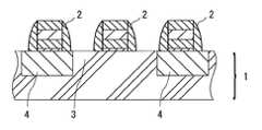
一例として図1に、前記ソースおよび/またはドレインせり上げ構造を形成する前のD
RAMの部分構造を示す。
図1に示す通り、前記半導体シリコン基板1に加えて、前記半導体シリコン基板1上に
別途設けられたゲート配線2や、このゲート配線2を含む前記半導体シリコン基板上を覆
うシリコン窒化膜等を含む多層構造から、不必要なシリコン窒化膜をエッチング操作によ
り除去することにより、前記ソースおよび/またはドレインせり上げ構造を形成する前の
構造が得られる。
なお前記半導体シリコン基板1には、前記DRAMを動作させるのに必要な不純物拡散
構造3や酸化膜4等が公知の手段により設けられている。
次に図2に示す様に、半導体シリコン基板表面と、前記ゲート配線のシリコン窒化膜側
壁とから形成される領域に対して選択エピタキシャル成長操作を実施することにより、前
記ソースおよび/またはドレインせり上げ構造501を形成することができると考えられ
る。With the recent reduction in size and weight of electronic and electrical components, the structure of a semiconductor device such as a DRAM having memory cells has been further miniaturized. In a semiconductor device having such a fine structure, since the influence of the electric field applied to the source and drain regions is not small, the source and the source provided on the semiconductor silicon substrate are for the purpose of mitigating the influence of the electric field. A drain raised structure has been adopted.
Such a raised structure of the source and / or drain is an LDD (lighty doped drain).
) And an impurity diffusion structure called STI (shallow trench isolation) and an oxide film such as an element isolation region called STI (shallow trench isolation) are usually provided on a semiconductor silicon substrate.
As an example, in FIG. 1, D before the source and / or drain raised structure is formed.
The partial structure of RAM is shown.
As shown in FIG. 1, in addition to the
The
Next, as shown in FIG. 2, by performing selective epitaxial growth operation on a region formed from the surface of the semiconductor silicon substrate and the side wall of the silicon nitride film of the gate wiring, the raised structure of the source and / or
しかし実際に選択エピタキシャル成長操作を実施すると、図2に示す理想的な前記ソー
スおよび/またはドレインせり上げ構造501は得られず、前記半導体シリコン基板に設
けられたSTIの端部にファセットと呼ばれる<111>面もしくは<311>面の面方
位を有する傾斜が発生することがある。図3を例に挙げて説明すれば、図3における傾斜
部分6がファセットに対応する。However, when the selective epitaxial growth operation is actually performed, the ideal source and / or drain raised
この様なファセットが発生すると次の様な問題が生じる。
すなわち、図3の上部から前記半導体シリコン基板1に対して各種イオン注入等の操作
を実施すると、ファセットの生じていない部分とファセットの生じている部分とでは、そ
れぞれ到達する各種イオンの深度方向の分布がばらつくため、前記半導体シリコン基板に
対する各種イオン注入の制御が困難であった。When such facets occur, the following problems occur.
That is, when various operations such as ion implantation are performed on the
図4は前記ソースおよび/またはドレインせり上げ構造501、502にそれぞれコン
タクト7を設けた様子を模式的に示したものである。なお図4において特に図示していな
いが、前記コンタクト7の周囲には酸化膜が設けられている。
図4に示す通り、前記ソースおよび/またはドレインせり上げ構造501、502を設
置した後、前記ソースおよび/またはドレインに対してタングステン等によるコンタクト
7を設けた場合、前記コンタクト毎に、前記ソースおよび/またはドレインせり上げ構造
と前記コンタクト7との接触面積が異なることから、前記コンタクト毎に抵抗が異なる場
合があった。
さらには前記接触面積が異なることに加えて、前記コンタクト7の底面毎に前記半導体
シリコン基板1に対する距離にばらつきが出ることから、前記コンタクトからしみ出した
不純物が前記半導体シリコン基板に与える影響もこれに伴いばらつく場合があった。FIG. 4 schematically shows a state in which
As shown in FIG. 4, after the source and / or drain raised
Further, in addition to the difference in the contact area, the distance to the
前記ファセットがもたらすこれらの要因から、最終的に得られた半導体装置の性能が安
定しないという問題があった。
この問題は前記ファセットの発生により生じることから、かかるファセットの発生を抑
えるべく、前記ゲート配線の側壁を二種類の酸化膜から形成しかつその形状を工夫する提
案がなされている(特許文献1)。
Since this problem is caused by the occurrence of the facets, a proposal has been made to devise the shape of the sidewalls of the gate wiring from two types of oxide films in order to suppress the occurrence of the facets (Patent Document 1). .
しかしながら、前記ゲート配線の側壁の形状等によりファセットの発生を抑える手段では、半導体装置の構造が微細化すればするほどこの手段は煩雑となる。またファセットが実際に発生してしまうと前記手段では発生してしまったファセットに基づく不具合に対応することができないという問題があった。
本発明の課題は、ファセットが生じた場合であっても、安定した性能を示す半導体装置の製造方法を提供することにある。However, the means for suppressing the occurrence of facets due to the shape of the side wall of the gate wiring and the like becomes more complicated as the structure of the semiconductor device is miniaturized. Further, when facets are actually generated, there is a problem that the above-mentioned means cannot cope with a problem based on the facets that have occurred.
An object of the present invention, even when the facet occurs, is to provide a manufacturing methodof a semiconductorequipment showing a stable performance.
本発明者は前記課題を解決するため鋭意検討した結果、ファセットのないソースおよび
/またはドレインせり上げ構造ではなく、下記の特定形状のファセットを備えたソースお
よび/またはドレインせり上げ構造を含む半導体装置が安定した性能を示すことを見出し
、本発明を完成するに至った。As a result of diligent investigations by the present inventor to solve the above problems, a semiconductor device including a source and / or drain raised structure having a facet having a specific shape described below instead of a source and / or drain raised structure having no facet. Was found to show stable performance, and the present invention was completed.
すなわち、本発明は、
[1]
(1)半導体シリコン基板に不純物拡散構造および素子分離領域を設置する工程と、
(2)半導体シリコン基板上にゲート配線を設置する工程と、
(3)半導体シリコン基板上に、選択エピタキシャル成長法により前記ゲート配線の側壁に接して半導体結晶をせり上げて成長させる工程と、
を含む半導体装置の製造方法であって、
前記半導体結晶をせり上げて成長させる工程は、少なくとも二段階の温度条件下および/または少なくとも二段階の圧力条件下により実施され、
前記少なくとも二段階の温度条件および/または少なくとも二段階の圧力条件が、
下記(a)〜(c)からなる群より選ばれる少なくとも一つであることを特徴とする半導体装置の製造方法であり、
(a)圧力は1〜100Torrの範囲で一定の値の下、第一の温度条件は830〜900℃の範囲であり、第二の温度条件は780〜820℃の範囲であること
(b)温度は780〜900℃の範囲で一定の値の下、第一の圧力条件は1〜10Torrの範囲であり、第二の圧力条件は20〜100Torrの範囲であること
(c)第一の温度および圧力条件は、それぞれ830〜900℃および1〜10Torrの範囲であり、第二の温度および圧力条件は、それぞれ780〜820℃および20〜100Torrの範囲であること
[2]前記選択エピタキシャル成長法に用いるガスがSiH2Cl2およびHClの混合ガスであることを特徴とする上記[1]に記載の半導体装置の製造方法である。
That is, the present invention
[1]
( 1) installing an impurity diffusion structure and an element isolation region in a semiconductor silicon substrate;
(2) a step of installing gate wiring on the semiconductor silicon substrate;
(3) a step of growing a semiconductor crystal on the semiconductor silicon substrate by contact witha side wall of the gate wiring by a selective epitaxial growth method;
A method of manufacturing a semiconductor device including:
The step of raising and growing the semiconductor crystal is performed under at least two stages of temperature conditions and / or at least two stages of pressure conditions;
Temperature conditions and / or at least two-stage pressure conditionsbefore Symbol least two stages,
A preparationhow thesemi conductor deviceyou being at least one selected from the group consisting of: (a) ~ (c),
(A) The pressure is within a range of 1 to 100 Torr, the first temperature condition is in the range of 830 to 900 ° C., and the second temperature condition is in the range of 780 to 820 ° C. (b) The temperature is a constant value in the range of 780 to 900 ° C., the first pressure condition is in the range of 1 to 10 Torr, and the second pressure condition is in the range of 20 to 100 Torr. (C) First temperature And pressure conditions are in the range of 830 to 900 ° C. and 1 to 10 Torr, respectively, and the second temperature and pressure conditions are in the range of 780 to 820 ° C. and 20 to 100 Torr, respectively. [2 ] In the selective epitaxial growth method gas usedis preparedhow the semiconductor device accordingto [1], which is a mixed gas of SiH2 Cl2 and HCl.
本発明によれば、例えば図8に示す通り、前記酸化膜および前記ゲート配線により区画
された部分8の形状と略同一の上端形状504を有する前記ソースおよび/またはドレイ
ンせり上げ構造503、506に例示される、前記ソースおよび/またはドレインせり上
げ構造を備えた半導体装置を提供することができる。これにより安定した性能を示す半導
体を提供することができる。According to the present invention, for example, as shown in FIG. 8, the source and / or drain raised
本発明を実施するための最良の形態について、以下に図面を参照しつつ説明する。
図5は、前記ソースおよび/またはドレインせり上げ構造を形成する前の構造を前記半
導体シリコン基板の上面から見た要部平面図を示している。The best mode for carrying out the present invention will be described below with reference to the drawings.
FIG. 5 shows a plan view of the main part of the structure before the source and / or drain raised structure is seen from the upper surface of the semiconductor silicon substrate.
図5において、黒い線はゲート配線2を示し、前記ゲート配線2の下に見える長方形に
より囲まれた部分は半導体シリコン基板の表面が露出した部分8を示し、前記ゲート配線
2と半導体シリコン基板の表面が露出した部分8以外の部分はSTI等の酸化膜4を示し
ている。
なお、図5においては、前記ゲート配線2は前記半導体シリコン基板の表面が露出した
部分8に対して斜めになった場合を図示しているが、図5に示した態様の場合に加えて、
前記ゲート配線8と前記半導体シリコン基板の表面が露出した部分8とのなす角度は任意
に設定することができる。In FIG. 5, the black line indicates the
5 shows the case where the
An angle formed by the
本発明に使用する半導体シリコン基板に特に限定はなく、通常半導体用途に用いられる
ものを使用することができる。この様な半導体シリコン基板は公知であり、市販品として
入手することが可能である。There is no limitation in particular in the semiconductor silicon substrate used for this invention, The thing normally used for a semiconductor use can be used. Such a semiconductor silicon substrate is known and can be obtained as a commercial product.
また本発明に使用する前記半導体シリコン基板は、所定の位置に酸化膜を備えているこ
とが必要である。
図6は、先の図5の一点破線をa−aの方向に切断した断面図を模式的に表したもので
ある。
図6に例示した通り、前記半導体シリコン基板はLDD等の不純物拡散構造3やSTI
等の酸化膜4等を備えたものである。
前記酸化膜の具体例としては、例えば酸化シリコン等を挙げることができる。Further, the semiconductor silicon substrate used in the present invention needs to have an oxide film at a predetermined position.
FIG. 6 schematically shows a cross-sectional view in which the one-dot broken line in FIG. 5 is cut in the direction aa.
As illustrated in FIG. 6, the semiconductor silicon substrate includes an
The
Specific examples of the oxide film include silicon oxide.
また、本発明に使用する半導体シリコン基板上にはゲート配線が設けられていることが
必要である。
図7は、前記図5の一点破線をb−b方向に切断した断面図を模式的に表したものであ
る。
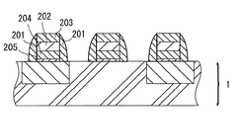
図7に例示される様に、本発明に使用するゲート配線は、多結晶半導体204および金
属からなるゲート電極、または、多結晶半導体204および金属シリサイド202からな
るゲート電極に加えて、側壁201、ゲート酸化膜205、コンタクト(図示せず)等に
より構成される。
本発明におけるゲート配線は絶縁膜により絶縁されたものであるが、この様な絶縁膜と
しては、例えば、窒化シリコン等を挙げることができる。
図7におけるゲート配線のうち、前記側壁201および上部構造203は窒化シリコン
等の絶縁膜が設けられている。Further, it is necessary that a gate wiring be provided on the semiconductor silicon substrate used in the present invention.
FIG. 7 schematically shows a cross-sectional view in which the one-dot broken line in FIG. 5 is cut in the bb direction.
As illustrated in FIG. 7, the gate wiring used in the present invention includes a
The gate wiring in the present invention is insulated by an insulating film, and examples of such an insulating film include silicon nitride.
Of the gate wiring in FIG. 7, the
次に本発明の半導体装置は、前記半導体シリコン基板上にソースおよび/またはドレイ
ンせり上げ構造を備えることが必要である。
図6における前記LDD3の上面部分8には特に保護膜等はなく、半導体シリコン基板
1の表面が露出された状態にある。
本発明の半導体装置に使用されるソースおよび/またはドレインせり上げ構造は、図8
に例示される様に、図6の前記LDD3の上面部分8に対し、選択エピタキシャル成長操
作を施して得られるものである。
前記LDD3の上面部分8は、図5に例示された、前記酸化膜4および前記ゲート配線
2により区画された前記半導体シリコン基板上の所定の位置に対応するものである。Next, the semiconductor device of the present invention is required to have a raised source and / or drain structure on the semiconductor silicon substrate.
The
The raised source and / or drain structure used in the semiconductor device of the present invention is shown in FIG.
As illustrated in FIG. 6, it is obtained by performing a selective epitaxial growth operation on the
The
図8に例示される様に、本発明の半導体に使用される前記ソースおよび/またはドレイ
ンせり上げ構造503上端部の形状504の、前記半導体シリコン基板法線方向に沿った
前記半導体シリコン基板上に対する正射投影像は、対応する前記酸化膜および前記ゲート
配線により区画された前記半導体シリコン基板上の所定の形状と略一致するものである。
この所定の形状とは、図5の場合で説明すれば、前記酸化膜4および前記ゲート配線2
に囲まれた8に示す領域部分の形状を意味する。
前記ソースおよび/またはドレイン構造506についても同様である。As illustrated in FIG. 8, the
If the predetermined shape is described in the case of FIG. 5, the
This means the shape of the region shown in 8 surrounded by.
The same applies to the source and / or
これにより、前記ソースおよび/またはドレインせり上げ構造の製造の際にファセット
が生じた場合であっても安定した性能を示す半導体を提供することができる。Thus, a semiconductor that exhibits stable performance can be provided even when facets are generated during the manufacture of the raised source and / or drain structure.
本発明においては、前記ソースおよび/またはドレインせり上げ構造のうち、前記半導
体シリコン基板1と平行な平面で切断して得られる断面の、前記半導体シリコン基板法線
方向に沿った前記半導体シリコン基板上に対する正射投影像の少なくとも一つは、対応す
る前記酸化膜および前記ゲート配線により区画された前記半導体シリコン基板上の所定形
状よりも大きいことが必要である。In the present invention, a cross section obtained by cutting the source and / or drain raised structure along a plane parallel to the
図8に例示する様に、前記ソースおよび/またはドレインせり上げ構造503の中程の
部分に外側に張り出す構造505を設けることにより、容易に所定の上端部形状504を
有する前記ソースおよび/またはドレインせり上げ構造503を得ることができ、これに
より安定した性能を示す半導体を提供することができる。As shown in FIG. 8, the source and / or drain having a predetermined
次に本発明の半導体装置の製造方法について説明する。
本発明の半導体装置を製造する方法は前記半導体シリコン基板に不純物拡散構造および
素子分離領域を設置する工程(1)を含むことが必要である。
本発明の製造方法に使用される前記半導体シリコン基板に特に限定はなく、公知のもの
を使用することができる。この様な半導体シリコン基板は市販品として入手可能である。
前記不純物拡散構造および素子分離領域を設置する工程(1)に特に限定はなく、前記
半導体シリコン基板を用いて通常実施される前処理工程により実施される方法であれば特
に限定はない。Next, a method for manufacturing a semiconductor device according to the present invention will be described.
The method for manufacturing a semiconductor device of the present invention needs to include the step (1) of installing an impurity diffusion structure and an element isolation region in the semiconductor silicon substrate.
There is no limitation in particular in the said semiconductor silicon substrate used for the manufacturing method of this invention, A well-known thing can be used. Such a semiconductor silicon substrate is available as a commercial product.
There is no particular limitation on the step (1) of installing the impurity diffusion structure and the element isolation region, and there is no particular limitation as long as it is a method performed by a pretreatment step that is normally performed using the semiconductor silicon substrate.
前記半導体シリコン基板に不純物拡散構造を設置する工程としては、例えば、具体的に
はCVD(Chemical Vapor Deposition)やイオン注入法工程
等を挙げることができる。これらの工程は一種もしくは二種以上を組合せて実施すること
ができる。Specific examples of the step of installing the impurity diffusion structure in the semiconductor silicon substrate include CVD (Chemical Vapor Deposition) and an ion implantation method. These steps can be carried out singly or in combination of two or more.
また、前記半導体シリコン基板に素子分離領域を設置する工程は前記半導体ウエハに対
して行なうものであるが、この様な工程としては、例えば、洗浄、酸化、CVD、フォト
リソグラフィ、ドライエッチング、CMP等の工程を挙げることができる。これらの工程
は一種もしくは二種以上を組合せて実施することができる。Further, the step of providing the element isolation region on the semiconductor silicon substrate is performed on the semiconductor wafer. Examples of such steps include cleaning, oxidation, CVD, photolithography, dry etching, CMP, and the like. Can be mentioned. These steps can be carried out singly or in combination of two or more.
また、本発明の半導体装置を製造する方法は、半導体シリコン基板上にゲート配線を設
置する工程(2)を含むことが必要である。
かかるゲート配線は、ワード線からなるものであり、通常実施される方法に従って製造
することができる。
本発明に使用するゲート配線は、絶縁膜により絶縁されているものである。かかる絶縁
の素材としては、特性の面から窒化シリコンであることが好ましい。Moreover, the method for manufacturing the semiconductor device of the present invention needs to include the step (2) of installing a gate wiring on the semiconductor silicon substrate.
Such a gate wiring consists of a word line, and can be manufactured according to a method that is usually performed.
The gate wiring used in the present invention is insulated by an insulating film. The insulating material is preferably silicon nitride from the viewpoint of characteristics.
また、本発明の半導体装置を製造する方法は、半導体シリコン基板上に、選択エピタキ
シャル成長法により前記ゲート配線に接して半導体結晶をせり上げて成長させる工程(3
)を含むことが必要である。The method of manufacturing a semiconductor device of the present invention includes a step (3) of growing a semiconductor crystal on a semiconductor silicon substrate in contact with the gate wiring by a selective epitaxial growth method.
).
ここで前記半導体結晶をせり上げて成長させる工程は、前記選択エピタキシャル成長法
により実施されるものであるが、かかる選択エピタキシャル成長法としては、例えば、前
記半導体結晶を成長させるガス成分と、前記半導体結晶をエッチングするガス成分とを同
時に前記半導体シリコン基板に作用させる方法等を挙げることができる。Here, the step of raising and growing the semiconductor crystal is performed by the selective epitaxial growth method. Examples of the selective epitaxial growth method include a gas component for growing the semiconductor crystal, and the semiconductor crystal. Examples include a method in which an etching gas component is simultaneously applied to the semiconductor silicon substrate.
前記半導体結晶を成長させるガス成分としては、例えば前記半導体シリコン基板が半導
体シリコン基板を用いて製造されている場合には、SiH4、SiH2Cl2等を挙げる
ことができる。前半導体結晶を成長させるガス成分は、取り扱い性の面からSiH2Cl
2が好ましい。Examples of the gas component for growing the semiconductor crystal include SiH4 and SiH2 Cl2 when the semiconductor silicon substrate is manufactured using the semiconductor silicon substrate. The gas component for growing the pre-semiconductor crystal is SiH2 Cl in terms of handleability.
2 is preferred.
前記半導体結晶をエッチングするガス成分としては、例えば前記半導体シリコン基板が
シリコンウエハを用いて製造されている場合には、HF、HCl等のハロゲン含有化合物
等を挙げることができる。前記半導体結晶をエッチングするガス成分としては、取り扱い
性の面からHClが好ましい。Examples of the gas component for etching the semiconductor crystal include halogen-containing compounds such as HF and HCl when the semiconductor silicon substrate is manufactured using a silicon wafer. As a gas component for etching the semiconductor crystal, HCl is preferable from the viewpoint of handleability.
前記半導体シリコン基板に作用させる上記ガス成分の体積比は、前半導体結晶を成長さ
せるガス成分と前記半導体結晶をエッチングするガス成分との比で、10:1〜10:8
の範囲であれば好ましい。The volume ratio of the gas component that acts on the semiconductor silicon substrate is a ratio of a gas component that grows a pre-semiconductor crystal and a gas component that etches the semiconductor crystal, and is 10: 1 to 10: 8.
If it is the range, it is preferable.
また前記エピタキシャル成長法は少なくとも二段階の温度条件下および/または圧力条
件下により実施されることが必要である。The epitaxial growth method needs to be performed under at least two-stage temperature conditions and / or pressure conditions.
前記二段階の温度条件および/または圧力条件としては、例えば、具体的には次のもの
を挙げることができる。
(a)圧力は1〜100Torrの範囲で一定の値に設定しておき、第一の温度条件は8
30〜900℃の範囲により選択エピタキシャル成長法を実施し、第二の温度条件は78
0〜820℃の範囲により選択エピタキシャル成長法を実施する場合
(b)温度は780〜900℃の範囲で一定の値に設定しておき、第一の圧力条件は1〜
10Torrの範囲により選択エピタキシャル成長法を実施し、第二の圧力条件は20〜
100Torrの範囲により選択エピタキシャル成長法を実施する場合
(c)第一の温度および圧力条件は、それぞれ830〜900℃および1〜10Torr
の範囲により選択エピタキシャル成長法を実施し、第二の温度および圧力条件は、それぞ
れ780〜820℃および20〜100Torrの範囲により選択エピタキシャル成長法
を実施する場合
上記(a)〜(c)等の条件は、一種もしくは二種以上を組合せて実施することができ
る。Specific examples of the two-stage temperature condition and / or pressure condition include the following.
(A) The pressure is set to a constant value in the range of 1 to 100 Torr, and the first temperature condition is 8
The selective epitaxial growth method is performed in the range of 30 to 900 ° C., and the second temperature condition is 78
When the selective epitaxial growth method is performed in the range of 0 to 820 ° C. (b) The temperature is set to a constant value in the range of 780 to 900 ° C., and the first pressure condition is 1 to
The selective epitaxial growth method is performed in the range of 10 Torr, and the second pressure condition is 20 to 20
When performing selective epitaxial growth in the range of 100 Torr (c) First temperature and pressure conditions are 830 to 900 ° C. and 1 to 10 Torr, respectively.
In the case where the selective epitaxial growth method is performed in the range of 780 to 820 ° C. and 20 to 100 Torr, respectively, the conditions of the above (a) to (c) are as follows. , One or a combination of two or more can be carried out.
上記(a)または(c)の第一の温度条件に示される様に、まず最初に830〜900
℃の範囲により選択エピタキシャル成長法を実施することにより、主として縦方向に選択
エピタキシャル成長を行なうことができる。
また、上記(b)または(c)の第一の圧力条件に示される様に、まず最初に1〜10
Torrの範囲により選択エピタキシャル成長法を実施することにより、主として縦方向
に選択エピタキシャル成長を行なうことができる。As shown in the first temperature condition (a) or (c) above, first, 830-900
By performing the selective epitaxial growth method in the range of ° C., selective epitaxial growth can be performed mainly in the vertical direction.
Further, as shown in the first pressure condition (b) or (c) above, first, 1 to 10
By performing the selective epitaxial growth method in the range of Torr, selective epitaxial growth can be performed mainly in the vertical direction.
さらに、上記(a)または(c)の第二の温度条件に示される様に、780〜820℃
の範囲により選択エピタキシャル成長法を実施することにより、主として横方向に選択エ
ピタキシャル成長を行なうことができる。
また、上記(b)または(c)の第二の圧力条件に示される様に、20〜100Tor
rの範囲により選択エピタキシャル成長法を実施することにより、主として横方向に選択
エピタキシャル成長を行なうことができる。Further, as shown in the second temperature condition (a) or (c) above, 780 to 820 ° C.
By carrying out the selective epitaxial growth method within the range, selective epitaxial growth can be performed mainly in the lateral direction.
Further, as shown in the second pressure condition (b) or (c) above, 20 to 100 Torr
By performing the selective epitaxial growth method within the range of r, selective epitaxial growth can be performed mainly in the lateral direction.
(a)に示される圧力は5〜30Torrの範囲であり、第一の温度条件は840〜8
70℃の範囲であり、第二の温度条件は790〜810℃の範囲であれば好ましい。
(b)に示される温度は800〜870℃の範囲であり、第一の圧力条件は3〜8To
rrの範囲であり、第二の圧力条件は25〜30Torrの範囲であれば好ましい。
(c)に示される温度および圧力条件は、それぞれ840〜870℃および3〜8To
rrの範囲によりエピタキシャル成長法を実施し、第二の温度および圧力条件は、それぞ
れ790〜810℃および25〜30Torrの範囲であれば好ましい。The pressure shown in (a) is in the range of 5-30 Torr, and the first temperature condition is 840-8.
It is in the range of 70 ° C, and the second temperature condition is preferably in the range of 790 to 810 ° C.
The temperature shown in (b) is in the range of 800-870 ° C., and the first pressure condition is 3-8 To.
The second pressure condition is preferably in the range of 25 to 30 Torr.
The temperature and pressure conditions shown in (c) are 840-870 ° C. and 3-8 To, respectively.
The epitaxial growth method is carried out in the range of rr, and the second temperature and pressure conditions are preferably in the range of 790 to 810 ° C. and 25 to 30 Torr, respectively.
この方法により、図8に例示した様に、前記LDD3の上面部分8の形状と、前記ソー
スおよび/またはドレインせり上げ構造503上端部の形状504とが略一致した前記ソ
ースおよび/またはドレインせり上げ構造を製造することができる。
前記ソースおよび/またはドレインせり上げ構造506についても同様である。By this method, as illustrated in FIG. 8, the source and / or drain lifted up so that the shape of the
The same applies to the source and / or drain raised
この様にして得られた前記ソースおよび/またはドレインせり上げ構造を備えた半導体
シリコン基板は、適宜ウエハ処理工程、配線工程、組立工程等の公知の処理を施された後
、例えば、DRAM(Dynamic Random Acsess memory)等
の半導体装置とすることができる。
この製造方法により、本発明の半導体装置が得られる。The thus obtained semiconductor silicon substrate having the raised source and / or drain structure is appropriately subjected to known processes such as a wafer processing process, a wiring process, an assembly process, etc., and then, for example, a DRAM (Dynamic A semiconductor device such as a random access memory) may be used.
With this manufacturing method, the semiconductor device of the present invention is obtained.
次に本発明について実施例を用いてさらに詳細に説明するが、本発明はこれらの実施例
により何ら限定されるものではない。EXAMPLES Next, although this invention is demonstrated further in detail using an Example, this invention is not limited at all by these Examples.
図9に示した通り、半導体シリコン基板1に不純物拡散構造3であるLDDと、酸化膜
4であるSTIとを設けた。
このシリコンウエハ上にゲート配線の基本構成を設け、前記ゲート配線の全体を窒化シ
リコンにより覆った。
続いて図10に示される様に、不必要な前記窒化シリコンをエッチングにより除去し、
前記半導体シリコン基板1上にゲート配線2を製造した。なお図10は前記ゲート配線2
の配線方向に対し、垂直方向に切断した断面を模式的に表したものである。As shown in FIG. 9, the
A basic structure of the gate wiring was provided on the silicon wafer, and the entire gate wiring was covered with silicon nitride.
Subsequently, as shown in FIG. 10, unnecessary silicon nitride is removed by etching,
A
The cross section cut | disconnected perpendicularly | vertically with respect to this wiring direction is represented typically.
次に図10に示される半導体シリコン基板表面が露出した部分8に対して選択エピタキ
シャル成長法を実施し、図11における半導体シリコン基板表面が露出した部分8上にソ
ースせり上げ構造506およびドレインせり上げ構造507を形成した。
なお図10における前記シリコンウエハ表面が露出した部分8は、前記シリコンウエハ
上の前記酸化膜4および前記ゲート配線2により区画されている。Next, selective epitaxial growth is performed on the
In FIG. 10, the exposed
前記選択エピタキシャル成長法は次の条件により実施した。すなわち、まず第一段階と
して850℃、15Torrの条件下、SiH2Cl2とHClとをそれぞれ200ml
/分、120ml/分の流量により前記半導体シリコン基板1の表面が露出した部分8に
対して選択エピタキシャル成長を実施した。この第一段階の操作により、前記半導体シリ
コン基板の8の上に、シリコンによる50nmの高さのせり上げ構造を得た。
続いて、第二段階として、800℃、15Torrの条件下、SiH2Cl2とHCl
とをそれぞれ200ml/分、80ml/分の流量により選択エピタキシャル成長を実施
した。この第二段階の操作により、前記シリコンによる50nmの高さのせり上げ構造の
上に、さらに20nmのシリコンをせり上げた。The selective epitaxial growth method was performed under the following conditions. That is, as a first step, 200 ml each of SiH2 Cl2 and HCl under conditions of 850 ° C. and 15 Torr.
Selective epitaxial growth was performed on the
Subsequently, as a second stage, SiH2 Cl2 and HCl are used under the conditions of 800 ° C. and 15 Torr.
Were selectively epitaxially grown at a flow rate of 200 ml / min and 80 ml / min, respectively. By this second stage operation, 20 nm of silicon was further lifted on the 50 nm high lifted structure of silicon.
これらの第一段階および第二段階による前記選択エピタキシャル成長法により得られた
、前記ソースせり上げ構造506および前記ドレインせり上げ構造507は、図11に示
す通り、その高さが70nmであるに対し、横方向の延びは20〜25nm程度であった
。The source raised
前記ソースせり上げ構造506および前記ドレインせり上げ構造507の上端部の形状
は、その半導体シリコン基板表面の法線方向に沿った、半導体シリコン基板表面上に対す
る正射投影像が、前記シリコンウエハ表面が露出した部分8と略一致するものである。
また、本実施例における図9における一点破線c−cによる切断面は、前記半導体シリ
コン基板表面が露出した部分8の形状よりも大きいものであった。The shape of the upper ends of the source raised
Further, the cut surface taken along the one-dot broken line cc in FIG. 9 in this example was larger than the shape of the
この様にして得られた前記ソースせり上げ構造506および前記ドレインせり上げ構造
507を備えたシリコンウエハに対し、ウエハ処理工程、配線工程、組立工程等の公知の
処理を実施することにより、DRAMを得た。得られたDRAMの特性は、製品毎のばら
つきが小さいものであった。By performing known processes such as a wafer processing process, a wiring process, and an assembling process on the silicon wafer provided with the source raised
実施例1の場合において、第一段階の温度条件と圧力条件をそれぞれ850℃、5To
rrとし、ならびに第二段階の温度条件と圧力条件をそれぞれ850℃、25Torrに
変更した以外は、実施例1と全く同様の操作を実施し、実施例1の場合と同様、図11に
記載の前記ソースせり上げ構造506および前記ドレインせり上げ構造507を有するD
RAMを得た。得られたDRAMの特性は、製品毎のばらつきが小さいものであった。In the case of Example 1, the temperature condition and pressure condition of the first stage are 850 ° C. and 5 To, respectively.
The same operation as in Example 1 was carried out except that rr and the temperature condition and pressure condition in the second stage were changed to 850 ° C. and 25 Torr, respectively. D having the source raised
I got RAM. The characteristics of the obtained DRAM had small variations among products.
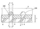
[比較例1]
実施例1の場合において、第一段階の条件を、温度850℃、圧力15Torrとし、
SiH2Cl2とHClとをそれぞれ200ml/分、120ml/分の流量とし、第二
段階による操作を省略した他は、実施例1の場合と同様の操作を実施した。
得られたDRAMは、図12に記載のソースせり上げ構造508およびドレインせり上
げ構造509を有するものであった。
図12における一点破線d−d間同士の距離は、一点破線e−e間同士の距離に比較し
て狭くなっている。
得られたDRAMの特性は得られる製品毎にばらつきが大きいものであった。[Comparative Example 1]
In the case of Example 1, the conditions of the first stage are a temperature of 850 ° C. and a pressure of 15 Torr,
The same operation as in Example 1 was performed, except that the flow rates of SiH2 Cl2 and HCl were 200 ml / min and 120 ml / min, respectively, and the operation in the second stage was omitted.
The obtained DRAM had the source raised
The distance between the dashed lines dd in FIG. 12 is narrower than the distance between the dashed lines ee.
The characteristics of the obtained DRAM varied greatly from product to product.
[比較例2]
実施例1の場合において、第一段階の条件を、温度800℃、圧力15Torrとし、
SiH2Cl2とHClとをそれぞれ200ml/分、80ml/分の流量とし、第二段
階による操作を省略した他は、実施例1の場合と同様の操作を実施した。
得られたDRAMは、図13に記載のソースせり上げ構造510およびドレインせり上
げ構造511を有するものであるが、図13の素子間分離領域4を超えて前記せり上げ構
造同士が接触しているため、動作不良を起こした。[Comparative Example 2]
In the case of Example 1, the first stage conditions were a temperature of 800 ° C. and a pressure of 15 Torr,
The same operation as in Example 1 was performed except that the flow rates of SiH2 Cl2 and HCl were 200 ml / min and 80 ml / min, respectively, and the operation in the second stage was omitted.
The obtained DRAM has the source raised
1 半導体シリコン基板
2 ゲート配線
201 側壁
202 金属シリサイド
203 窒化シリコン
204 多結晶半導体
205 ゲート酸化膜
3 不純物拡散構造
4 酸化膜
501、503、506、507、508、509、510、511 ソースせり上
げ構造またはドレインせり上げ構造
502 ファセットが生じたソースせり上げ構造またはドレインせり上げ構造
504 ソースせり上げ構造またはドレインせり上げ構造上端部
505 ソースせり上げ構造またはドレインせり上げ構造の張り出し部
6 ファセット
7 コンタクト
8 LDDの上面部分DESCRIPTION OF
Claims (2)
Translated fromJapanese(2)半導体シリコン基板上にゲート配線を設置する工程と、
(3)半導体シリコン基板上に、選択エピタキシャル成長法により前記ゲート配線の側壁に接して半導体結晶をせり上げて成長させる工程と、
を含む半導体装置の製造方法であって、前記半導体結晶をせり上げて成長させる工程は、少なくとも二段階の温度条件下および/または少なくとも二段階の圧力条件下により実施され、
前記少なくとも二段階の温度条件および/または少なくとも二段階の圧力条件が、下記(a)〜(c)からなる群より選ばれる少なくとも一つであることを特徴とする半導体装置の製造方法。
(a)圧力は1〜100Torrの範囲で一定の値の下、第一の温度条件は830〜900℃の範囲であり、第二の温度条件は780〜820℃の範囲であること
(b)温度は780〜900℃の範囲で一定の値の下、第一の圧力条件は1〜10Torrの範囲であり、第二の圧力条件は20〜100Torrの範囲であること
(c)第一の温度および圧力条件は、それぞれ830〜900℃および1〜10Torrの範囲であり、第二の温度および圧力条件は、それぞれ780〜820℃および20〜100Torrの範囲であること(1) installing an impurity diffusion structure and an element isolation region in a semiconductor silicon substrate;
(2) a step of installing gate wiring on the semiconductor silicon substrate;
(3) a step of growing a semiconductor crystal on the semiconductor silicon substrate by contact with a side wall of the gate wiring by a selective epitaxial growth method;
A step of raising and growing the semiconductor crystal is performed under at least two stages of temperature conditions and / or at least two stages of pressure conditions,
The method of manufacturing a semiconductor device, wherein the at least two stages of temperature conditions and / or at least two stages of pressure conditions are at least one selected from the group consisting of the following (a) to (c).
(A) The pressure is within a range of 1 to 100 Torr, the first temperature condition is in the range of 830 to 900 ° C., and the second temperature condition is in the range of 780 to 820 ° C. (b) The temperature is a constant value in the range of 780 to 900 ° C., the first pressure condition is in the range of 1 to 10 Torr, and the second pressure condition is in the range of 20 to 100 Torr. (C) First temperature And pressure conditions are in the range of 830-900 ° C. and 1-10 Torr, respectively, and the second temperature and pressure conditions are in the range of 780-820 ° C. and 20-100 Torr, respectively.
Priority Applications (6)
| Application Number | Priority Date | Filing Date | Title |
|---|---|---|---|
| JP2005125921AJP4274566B2 (en) | 2005-04-25 | 2005-04-25 | Manufacturing method of semiconductor device |
| TW095114687ATWI298540B (en) | 2005-04-25 | 2006-04-25 | Semiconductor device and method of manufacturing the same |
| US11/410,118US7482235B2 (en) | 2005-04-25 | 2006-04-25 | Semiconductor device and method of manufacturing the same |
| KR1020060037054AKR100745929B1 (en) | 2005-04-25 | 2006-04-25 | Semiconductor device and method of manufacturing the same |
| CNB2006100751631ACN100543995C (en) | 2005-04-25 | 2006-04-25 | Semiconductor device and manufacturing method thereof |
| US12/272,036US7906809B2 (en) | 2005-04-25 | 2008-11-17 | Semiconductor device having an elevated source/drain structure of varying cross-section |
Applications Claiming Priority (1)
| Application Number | Priority Date | Filing Date | Title |
|---|---|---|---|
| JP2005125921AJP4274566B2 (en) | 2005-04-25 | 2005-04-25 | Manufacturing method of semiconductor device |
Publications (2)
| Publication Number | Publication Date |
|---|---|
| JP2006303336A JP2006303336A (en) | 2006-11-02 |
| JP4274566B2true JP4274566B2 (en) | 2009-06-10 |
Family
ID=37187505
Family Applications (1)
| Application Number | Title | Priority Date | Filing Date |
|---|---|---|---|
| JP2005125921AExpired - Fee RelatedJP4274566B2 (en) | 2005-04-25 | 2005-04-25 | Manufacturing method of semiconductor device |
Country Status (5)
| Country | Link |
|---|---|
| US (2) | US7482235B2 (en) |
| JP (1) | JP4274566B2 (en) |
| KR (1) | KR100745929B1 (en) |
| CN (1) | CN100543995C (en) |
| TW (1) | TWI298540B (en) |
Families Citing this family (11)
| Publication number | Priority date | Publication date | Assignee | Title |
|---|---|---|---|---|
| JP2009088305A (en)* | 2007-10-01 | 2009-04-23 | Hitachi Kokusai Electric Inc | Manufacturing method of semiconductor device |
| JP5235142B2 (en)* | 2009-01-21 | 2013-07-10 | 株式会社日立国際電気 | Semiconductor device manufacturing method and substrate processing apparatus |
| US8415718B2 (en)* | 2009-10-30 | 2013-04-09 | Taiwan Semiconductor Manufacturing Company, Ltd. | Method of forming epi film in substrate trench |
| KR20130102399A (en)* | 2012-03-07 | 2013-09-17 | 삼성전자주식회사 | Semiconductor device and method of manufacturing the same |
| US9397098B2 (en) | 2012-03-08 | 2016-07-19 | Taiwan Semiconductor Manufacturing Company, Ltd. | FinFET-based ESD devices and methods for forming the same |
| US8779517B2 (en)* | 2012-03-08 | 2014-07-15 | Taiwan Semiconductor Manufacturing Company, Ltd. | FinFET-based ESD devices and methods for forming the same |
| KR20140016008A (en) | 2012-07-30 | 2014-02-07 | 삼성전자주식회사 | Semiconductor device and method of manufacturing the same |
| JP6235785B2 (en)* | 2013-03-18 | 2017-11-22 | 日本電子材料株式会社 | Probe card guide plate and probe card guide plate manufacturing method |
| KR102085525B1 (en) | 2013-11-27 | 2020-03-09 | 삼성전자 주식회사 | Semiconductor device and method for fabricating the same |
| KR102505245B1 (en) | 2016-08-17 | 2023-02-28 | 대우조선해양 주식회사 | Submarine |
| CN116417503B (en)* | 2021-12-31 | 2025-09-12 | 苏州能讯高能半导体有限公司 | A semiconductor device |
Family Cites Families (16)
| Publication number | Priority date | Publication date | Assignee | Title |
|---|---|---|---|---|
| US4404732A (en)* | 1981-12-07 | 1983-09-20 | Ibm Corporation | Self-aligned extended epitaxy mesfet fabrication process |
| US5182619A (en) | 1991-09-03 | 1993-01-26 | Motorola, Inc. | Semiconductor device having an MOS transistor with overlapped and elevated source and drain |
| US5371026A (en)* | 1992-11-30 | 1994-12-06 | Motorola Inc. | Method for fabricating paired MOS transistors having a current-gain differential |
| JP2964925B2 (en) | 1994-10-12 | 1999-10-18 | 日本電気株式会社 | Method of manufacturing complementary MIS type FET |
| US5753555A (en)* | 1995-11-22 | 1998-05-19 | Nec Corporation | Method for forming semiconductor device |
| JP2894283B2 (en)* | 1996-06-27 | 1999-05-24 | 日本電気株式会社 | Method for manufacturing semiconductor device |
| JP2964960B2 (en) | 1996-09-27 | 1999-10-18 | 日本電気株式会社 | Semiconductor device and manufacturing method thereof |
| JP2000049348A (en) | 1998-05-29 | 2000-02-18 | Toshiba Corp | Semiconductor device having elevated source / drain structure and method of manufacturing the same |
| US6232641B1 (en)* | 1998-05-29 | 2001-05-15 | Kabushiki Kaisha Toshiba | Semiconductor apparatus having elevated source and drain structure and manufacturing method therefor |
| JP4204671B2 (en)* | 1998-09-11 | 2009-01-07 | 三菱電機株式会社 | Manufacturing method of semiconductor device |
| KR20010061029A (en)* | 1999-12-28 | 2001-07-07 | 박종섭 | A method for forming MOSFET of elevated source/drain structure |
| KR100679203B1 (en)* | 2000-01-07 | 2007-02-07 | 샤프 가부시키가이샤 | Semiconductor device, manufacturing method thereof, and information processing device |
| KR100496258B1 (en)* | 2003-02-17 | 2005-06-17 | 삼성전자주식회사 | semiconductor device having a contact pad and method for a same |
| US6872606B2 (en)* | 2003-04-03 | 2005-03-29 | Taiwan Semiconductor Manufacturing Company, Ltd. | Semiconductor device with raised segment |
| US7253086B2 (en)* | 2004-10-18 | 2007-08-07 | Texas Instruments Incorporated | Recessed drain extensions in transistor device |
| US20060088966A1 (en)* | 2004-10-21 | 2006-04-27 | Taiwan Semiconductor Manufacturing Company, Ltd. | Semiconductor device having a smooth EPI layer and a method for its manufacture |
- 2005
- 2005-04-25JPJP2005125921Apatent/JP4274566B2/ennot_activeExpired - Fee Related
- 2006
- 2006-04-25TWTW095114687Apatent/TWI298540B/enactive
- 2006-04-25USUS11/410,118patent/US7482235B2/enactiveActive
- 2006-04-25CNCNB2006100751631Apatent/CN100543995C/ennot_activeExpired - Fee Related
- 2006-04-25KRKR1020060037054Apatent/KR100745929B1/ennot_activeExpired - Fee Related
- 2008
- 2008-11-17USUS12/272,036patent/US7906809B2/enactiveActive
Also Published As
| Publication number | Publication date |
|---|---|
| TW200711135A (en) | 2007-03-16 |
| US7482235B2 (en) | 2009-01-27 |
| TWI298540B (en) | 2008-07-01 |
| KR20060111858A (en) | 2006-10-30 |
| US20060240657A1 (en) | 2006-10-26 |
| CN100543995C (en) | 2009-09-23 |
| US7906809B2 (en) | 2011-03-15 |
| US20090072324A1 (en) | 2009-03-19 |
| CN1855492A (en) | 2006-11-01 |
| JP2006303336A (en) | 2006-11-02 |
| KR100745929B1 (en) | 2007-08-02 |
Similar Documents
| Publication | Publication Date | Title |
|---|---|---|
| US10665669B1 (en) | Insulative structure with diffusion break integral with isolation layer and methods to form same | |
| KR100745929B1 (en) | Semiconductor device and method of manufacturing the same | |
| US20210183997A1 (en) | Gate cut isolation including air gap, integrated circuit including same and related method | |
| US7439138B2 (en) | Method of forming integrated circuitry | |
| US10734525B2 (en) | Gate-all-around transistor with spacer support and methods of forming same | |
| KR102451417B1 (en) | Semiconductor devices | |
| TWI776954B (en) | Method of forming a semiconductor structure and semiconductor structure | |
| US10157794B1 (en) | Integrated circuit structure with stepped epitaxial region | |
| US20090233411A1 (en) | Semiconductor device and method of manufacturing semiconductor device | |
| US10629699B2 (en) | Gate height control and ILD protection | |
| CN109148582B (en) | Method for laterally etching epitaxial layer | |
| KR20170124063A (en) | Semiconductor device and method for fabricating the same | |
| US12068162B2 (en) | Semiconductor device and method | |
| US20060237766A1 (en) | Semiconductor device using solid phase epitaxy and method for fabricating the same | |
| KR20110083465A (en) | Transistor Formation Using Capping Layer | |
| KR100517328B1 (en) | Semiconductor device having contact plug using selective epitaxial growth and method of fabricating the same | |
| US20030068885A1 (en) | Method of forming a contact plug for a semiconductor device | |
| KR102085324B1 (en) | Contact plugs and methods of forming same | |
| US20230361199A1 (en) | Replacement sidewall spacers | |
| US11217584B2 (en) | Limiting lateral epitaxy growth at N-P boundary using inner spacer, and related structure | |
| US20240071812A1 (en) | Embedded soi structure for low leakage mos capacitor | |
| KR20080029574A (en) | Method of forming recessed contact plug of semiconductor device by in-situ etching method | |
| WO2022256098A1 (en) | Sacrificial capping layer for contact etch | |
| TW202318565A (en) | Method of fabricating semiconductor device | |
| KR100196217B1 (en) | Forming method for plug |
Legal Events
| Date | Code | Title | Description |
|---|---|---|---|
| RD01 | Notification of change of attorney | Free format text:JAPANESE INTERMEDIATE CODE: A7421 Effective date:20070618 | |
| A977 | Report on retrieval | Free format text:JAPANESE INTERMEDIATE CODE: A971007 Effective date:20081128 | |
| A131 | Notification of reasons for refusal | Free format text:JAPANESE INTERMEDIATE CODE: A131 Effective date:20081210 | |
| A521 | Request for written amendment filed | Free format text:JAPANESE INTERMEDIATE CODE: A523 Effective date:20090204 | |
| TRDD | Decision of grant or rejection written | ||
| A01 | Written decision to grant a patent or to grant a registration (utility model) | Free format text:JAPANESE INTERMEDIATE CODE: A01 Effective date:20090225 | |
| A01 | Written decision to grant a patent or to grant a registration (utility model) | Free format text:JAPANESE INTERMEDIATE CODE: A01 | |
| A61 | First payment of annual fees (during grant procedure) | Free format text:JAPANESE INTERMEDIATE CODE: A61 Effective date:20090302 | |
| R150 | Certificate of patent or registration of utility model | Free format text:JAPANESE INTERMEDIATE CODE: R150 | |
| FPAY | Renewal fee payment (event date is renewal date of database) | Free format text:PAYMENT UNTIL: 20120313 Year of fee payment:3 | |
| FPAY | Renewal fee payment (event date is renewal date of database) | Free format text:PAYMENT UNTIL: 20120313 Year of fee payment:3 | |
| FPAY | Renewal fee payment (event date is renewal date of database) | Free format text:PAYMENT UNTIL: 20130313 Year of fee payment:4 | |
| FPAY | Renewal fee payment (event date is renewal date of database) | Free format text:PAYMENT UNTIL: 20130313 Year of fee payment:4 | |
| FPAY | Renewal fee payment (event date is renewal date of database) | Free format text:PAYMENT UNTIL: 20140313 Year of fee payment:5 | |
| S111 | Request for change of ownership or part of ownership | Free format text:JAPANESE INTERMEDIATE CODE: R313113 | |
| R350 | Written notification of registration of transfer | Free format text:JAPANESE INTERMEDIATE CODE: R350 | |
| R250 | Receipt of annual fees | Free format text:JAPANESE INTERMEDIATE CODE: R250 | |
| R250 | Receipt of annual fees | Free format text:JAPANESE INTERMEDIATE CODE: R250 | |
| LAPS | Cancellation because of no payment of annual fees |