JP4274554B2 - Element substrate and method for forming liquid ejection element - Google Patents
Element substrate and method for forming liquid ejection elementDownload PDFInfo
- Publication number
- JP4274554B2 JP4274554B2JP2004210086AJP2004210086AJP4274554B2JP 4274554 B2JP4274554 B2JP 4274554B2JP 2004210086 AJP2004210086 AJP 2004210086AJP 2004210086 AJP2004210086 AJP 2004210086AJP 4274554 B2JP4274554 B2JP 4274554B2
- Authority
- JP
- Japan
- Prior art keywords
- substrate
- forming
- supply port
- ink supply
- ink
- Prior art date
- Legal status (The legal status is an assumption and is not a legal conclusion. Google has not performed a legal analysis and makes no representation as to the accuracy of the status listed.)
- Expired - Fee Related
Links
Images


Classifications
- B—PERFORMING OPERATIONS; TRANSPORTING
- B41—PRINTING; LINING MACHINES; TYPEWRITERS; STAMPS
- B41J—TYPEWRITERS; SELECTIVE PRINTING MECHANISMS, i.e. MECHANISMS PRINTING OTHERWISE THAN FROM A FORME; CORRECTION OF TYPOGRAPHICAL ERRORS
- B41J2/00—Typewriters or selective printing mechanisms characterised by the printing or marking process for which they are designed
- B41J2/005—Typewriters or selective printing mechanisms characterised by the printing or marking process for which they are designed characterised by bringing liquid or particles selectively into contact with a printing material
- B41J2/01—Ink jet
- B41J2/135—Nozzles
- B41J2/16—Production of nozzles
- B41J2/1621—Manufacturing processes
- B41J2/164—Manufacturing processes thin film formation
- B41J2/1643—Manufacturing processes thin film formation thin film formation by plating
- B—PERFORMING OPERATIONS; TRANSPORTING
- B41—PRINTING; LINING MACHINES; TYPEWRITERS; STAMPS
- B41J—TYPEWRITERS; SELECTIVE PRINTING MECHANISMS, i.e. MECHANISMS PRINTING OTHERWISE THAN FROM A FORME; CORRECTION OF TYPOGRAPHICAL ERRORS
- B41J2/00—Typewriters or selective printing mechanisms characterised by the printing or marking process for which they are designed
- B41J2/005—Typewriters or selective printing mechanisms characterised by the printing or marking process for which they are designed characterised by bringing liquid or particles selectively into contact with a printing material
- B41J2/01—Ink jet
- B41J2/135—Nozzles
- B41J2/14—Structure thereof only for on-demand ink jet heads
- B41J2/14016—Structure of bubble jet print heads
- B41J2/14088—Structure of heating means
- B41J2/14112—Resistive element
- B—PERFORMING OPERATIONS; TRANSPORTING
- B41—PRINTING; LINING MACHINES; TYPEWRITERS; STAMPS
- B41J—TYPEWRITERS; SELECTIVE PRINTING MECHANISMS, i.e. MECHANISMS PRINTING OTHERWISE THAN FROM A FORME; CORRECTION OF TYPOGRAPHICAL ERRORS
- B41J2/00—Typewriters or selective printing mechanisms characterised by the printing or marking process for which they are designed
- B41J2/005—Typewriters or selective printing mechanisms characterised by the printing or marking process for which they are designed characterised by bringing liquid or particles selectively into contact with a printing material
- B41J2/01—Ink jet
- B41J2/135—Nozzles
- B41J2/16—Production of nozzles
- B41J2/1601—Production of bubble jet print heads
- B41J2/1603—Production of bubble jet print heads of the front shooter type
- B—PERFORMING OPERATIONS; TRANSPORTING
- B41—PRINTING; LINING MACHINES; TYPEWRITERS; STAMPS
- B41J—TYPEWRITERS; SELECTIVE PRINTING MECHANISMS, i.e. MECHANISMS PRINTING OTHERWISE THAN FROM A FORME; CORRECTION OF TYPOGRAPHICAL ERRORS
- B41J2/00—Typewriters or selective printing mechanisms characterised by the printing or marking process for which they are designed
- B41J2/005—Typewriters or selective printing mechanisms characterised by the printing or marking process for which they are designed characterised by bringing liquid or particles selectively into contact with a printing material
- B41J2/01—Ink jet
- B41J2/135—Nozzles
- B41J2/16—Production of nozzles
- B41J2/1621—Manufacturing processes
- B41J2/1626—Manufacturing processes etching
- B41J2/1628—Manufacturing processes etching dry etching
- B—PERFORMING OPERATIONS; TRANSPORTING
- B41—PRINTING; LINING MACHINES; TYPEWRITERS; STAMPS
- B41J—TYPEWRITERS; SELECTIVE PRINTING MECHANISMS, i.e. MECHANISMS PRINTING OTHERWISE THAN FROM A FORME; CORRECTION OF TYPOGRAPHICAL ERRORS
- B41J2/00—Typewriters or selective printing mechanisms characterised by the printing or marking process for which they are designed
- B41J2/005—Typewriters or selective printing mechanisms characterised by the printing or marking process for which they are designed characterised by bringing liquid or particles selectively into contact with a printing material
- B41J2/01—Ink jet
- B41J2/135—Nozzles
- B41J2/16—Production of nozzles
- B41J2/1621—Manufacturing processes
- B41J2/1632—Manufacturing processes machining
- B41J2/1634—Manufacturing processes machining laser machining
- Y—GENERAL TAGGING OF NEW TECHNOLOGICAL DEVELOPMENTS; GENERAL TAGGING OF CROSS-SECTIONAL TECHNOLOGIES SPANNING OVER SEVERAL SECTIONS OF THE IPC; TECHNICAL SUBJECTS COVERED BY FORMER USPC CROSS-REFERENCE ART COLLECTIONS [XRACs] AND DIGESTS
- Y10—TECHNICAL SUBJECTS COVERED BY FORMER USPC
- Y10T—TECHNICAL SUBJECTS COVERED BY FORMER US CLASSIFICATION
- Y10T29/00—Metal working
- Y10T29/49—Method of mechanical manufacture
- Y10T29/49002—Electrical device making
- Y10T29/49117—Conductor or circuit manufacturing
- Y10T29/49124—On flat or curved insulated base, e.g., printed circuit, etc.
- Y10T29/49126—Assembling bases
- Y—GENERAL TAGGING OF NEW TECHNOLOGICAL DEVELOPMENTS; GENERAL TAGGING OF CROSS-SECTIONAL TECHNOLOGIES SPANNING OVER SEVERAL SECTIONS OF THE IPC; TECHNICAL SUBJECTS COVERED BY FORMER USPC CROSS-REFERENCE ART COLLECTIONS [XRACs] AND DIGESTS
- Y10—TECHNICAL SUBJECTS COVERED BY FORMER USPC
- Y10T—TECHNICAL SUBJECTS COVERED BY FORMER US CLASSIFICATION
- Y10T29/00—Metal working
- Y10T29/49—Method of mechanical manufacture
- Y10T29/49002—Electrical device making
- Y10T29/49117—Conductor or circuit manufacturing
- Y10T29/49124—On flat or curved insulated base, e.g., printed circuit, etc.
- Y10T29/49128—Assembling formed circuit to base
- Y—GENERAL TAGGING OF NEW TECHNOLOGICAL DEVELOPMENTS; GENERAL TAGGING OF CROSS-SECTIONAL TECHNOLOGIES SPANNING OVER SEVERAL SECTIONS OF THE IPC; TECHNICAL SUBJECTS COVERED BY FORMER USPC CROSS-REFERENCE ART COLLECTIONS [XRACs] AND DIGESTS
- Y10—TECHNICAL SUBJECTS COVERED BY FORMER USPC
- Y10T—TECHNICAL SUBJECTS COVERED BY FORMER US CLASSIFICATION
- Y10T29/00—Metal working
- Y10T29/49—Method of mechanical manufacture
- Y10T29/49002—Electrical device making
- Y10T29/49117—Conductor or circuit manufacturing
- Y10T29/49124—On flat or curved insulated base, e.g., printed circuit, etc.
- Y10T29/4913—Assembling to base an electrical component, e.g., capacitor, etc.
- Y10T29/49139—Assembling to base an electrical component, e.g., capacitor, etc. by inserting component lead or terminal into base aperture
- Y—GENERAL TAGGING OF NEW TECHNOLOGICAL DEVELOPMENTS; GENERAL TAGGING OF CROSS-SECTIONAL TECHNOLOGIES SPANNING OVER SEVERAL SECTIONS OF THE IPC; TECHNICAL SUBJECTS COVERED BY FORMER USPC CROSS-REFERENCE ART COLLECTIONS [XRACs] AND DIGESTS
- Y10—TECHNICAL SUBJECTS COVERED BY FORMER USPC
- Y10T—TECHNICAL SUBJECTS COVERED BY FORMER US CLASSIFICATION
- Y10T29/00—Metal working
- Y10T29/49—Method of mechanical manufacture
- Y10T29/49401—Fluid pattern dispersing device making, e.g., ink jet
Landscapes
- Engineering & Computer Science (AREA)
- Manufacturing & Machinery (AREA)
- Physics & Mathematics (AREA)
- Optics & Photonics (AREA)
- Particle Formation And Scattering Control In Inkjet Printers (AREA)
Description
Translated fromJapanese本発明は、インクジェット方式の素子基板およびその製造方法に関し、特に電気熱変換素子を用いる方式の素子基板およびその製造方法に関する。 The present invention relates to an ink jet element substrate and a manufacturing method thereof, and more particularly to an element substrate using an electrothermal conversion element and a manufacturing method thereof.
インクジェット方式の記録方法は、インク吐出方式の違いから、ピエゾ素子等の電気機械変換素子を用いる方式、レーザー等の電磁波を照射してインクを発熱させ、この発熱による作用でインク滴を吐出させる方式、発熱抵抗体を有する電気熱変換素子によってインク滴を加熱して、インク滴を吐出させる方式などに分類される。電気熱変換素子を用いる方式のインクジェット記録方法は、熱エネルギーの作用を受けたインクが加熱されて気泡が生じ、気泡発生に基づく作用力によって、記録ヘッド部先端のオリフィスに液滴が形成され、その液滴が記録媒体に付着して情報の記録が行われるという原理に基づいている。すなわち、熱エネルギーをインクに作用させて、液滴吐出の原動力を得るという点において、他のインク吐出方式とは異なる特徴を有している(特許文献1参照。)。 Inkjet recording methods include the use of electromechanical transducers such as piezo elements due to differences in ink ejection methods, and the method of causing ink to generate heat by irradiating electromagnetic waves such as laser and ejecting ink droplets by the action of this heat generation. The ink droplets are heated by an electrothermal conversion element having a heating resistor, and the ink droplets are ejected. Ink jet recording method using an electrothermal conversion element is a method in which ink subjected to the action of heat energy is heated to generate bubbles, and droplets are formed at the orifice at the tip of the recording head by the action force based on the generation of bubbles, This is based on the principle that the droplets adhere to the recording medium and information is recorded. That is, it has a feature that is different from other ink ejection methods in that thermal energy is applied to ink to obtain a driving force for droplet ejection (see Patent Document 1).
電気熱変換素子を用いる方式のインクジェット記録方法に適用される液体吐出素子は、一般的に600μm程度の厚さを有している基板上に、インク供給口と、インク供給口に連通するインク液吐出部と、熱エネルギーを発生させる発熱抵抗層と、発熱抵抗層をインクから保護する上部保護層と、発生熱を蓄熱する下部層とを有している。また、インク液吐出部は、液体を吐出するオリフィスと、オリフィスに連通しオリフィスにインク液を供給するとともに、発熱抵抗層で発生した熱エネルギーをインク液に供給する熱作用部を備えた液流路とを有している。 A liquid discharge element applied to an ink jet recording method using an electrothermal conversion element generally includes an ink supply port and an ink liquid communicating with the ink supply port on a substrate having a thickness of about 600 μm. It has a discharge part, a heat generating resistor layer that generates thermal energy, an upper protective layer that protects the heat generating resistor layer from ink, and a lower layer that stores generated heat. In addition, the ink liquid discharge unit includes an orifice for discharging the liquid, a liquid flow unit that is connected to the orifice and supplies the ink liquid to the orifice, and a heat acting unit that supplies the heat energy generated in the heating resistance layer to the ink liquid. Road.
ところで、インクジェット記録方法においては、記録画像の品質の向上のために液流路、オリフィス、インク供給口等を高密度、高精度で形成する必要がある。このため、例えば、溶解可能な樹脂層を形成し、その上部に被覆層を形成し、被覆層にオリフィスを形成後、樹脂層を溶解して液流路を形成する方法(特許文献2,3参照。)や、オリフィスを形成後、インク供給口をエッチングで形成する方法(特許文献4参照。)などが開示されている。 By the way, in the ink jet recording method, it is necessary to form liquid flow paths, orifices, ink supply ports and the like with high density and high accuracy in order to improve the quality of a recorded image. For this reason, for example, a method of forming a liquid flow path by forming a soluble resin layer, forming a coating layer on the upper part, forming an orifice in the coating layer, and then dissolving the resin layer (
また、ヘッドの実装領域低減やコンパクト化のため、基板の表面(基板の発熱抵抗体が形成されている面)と裏面(反対側の面)とを貫通電極でつなげる方法(特許文献5、6参照。)も開示されている。
上述したとおり、記録画像の品質の向上のためには、インク供給口を高密度、高精度で形成する必要がある。また、ヘッドの実装領域低減やコンパクト化の観点から、基板の表面と裏面とを貫通電極でつなげる構成を取った場合に、そのメリットを十分に発揮するためには、貫通電極を高密度で、すなわち、貫通電極の穴径と配列ピッチの双方を低減して配列する必要がある。しかしながら、これらのインク供給口や貫通電極は厚い基板を貫通することから、従来技術において以下の問題があった。 As described above, in order to improve the quality of the recorded image, it is necessary to form the ink supply ports with high density and high accuracy. Also, from the viewpoint of reducing the mounting area of the head and making it more compact, when taking a configuration where the front and back surfaces of the substrate are connected by a through electrode, in order to fully demonstrate its merit, the through electrode must be dense, That is, it is necessary to reduce both the hole diameter and the arrangement pitch of the through electrodes. However, since these ink supply ports and through electrodes penetrate through a thick substrate, there are the following problems in the prior art.
(1)インク供給口は基板のエッチングによって形成されるが、基板が厚いと、インク供給口形成の精度が悪くなる。その理由は、基板が厚くなるほどインク供給口の平面方向、垂直方向の加工精度の確保が困難になるためである。その結果、発熱抵抗体とインク供給口との間の寸法のばらつきが大きくなり、吐出性能のばらつきが増大し、印字性能の悪化につながる。また、インク供給口の貫通厚さが大きいので加工時間が長くなり、製作効率が悪化するとともに、真空装置を長時間使用するためコストアップの可能性があった。 (1) The ink supply port is formed by etching the substrate. However, if the substrate is thick, the accuracy of forming the ink supply port deteriorates. The reason is that as the substrate becomes thicker, it becomes more difficult to ensure the processing accuracy in the plane direction and the vertical direction of the ink supply port. As a result, the dimensional variation between the heating resistor and the ink supply port is increased, the variation in the ejection performance is increased, and the printing performance is deteriorated. Further, since the penetrating thickness of the ink supply port is large, the processing time becomes long, the production efficiency deteriorates, and the use of the vacuum device for a long time may increase the cost.
(2)貫通電極を高密度で配列するには、貫通電極形成用の貫通穴を高密度で配列しなければならない。貫通穴は、レーザ、ドライエッチング等で形成されるが、基板の厚さが厚くなるほど、貫通穴を高密度に配列することが難しかった。その第1の理由は上記の(1)と同様、貫通穴の加工精度上の制約である。すなわち、基板の厚さが厚くなるほど貫通穴の径や垂直方向の加工精度の確保が困難になり、これによって穴径と配列ピッチが制約される。第2の理由は、貫通穴へのめっきの充填性の制約である。貫通穴にめっきによって金属を充填し貫通電極を形成する際に、同一の穴径で基板が厚くなると、穴径に対する深さが増え、貫通穴が細長の寸法比になるため、めっきの充填が困難となる。このため、厚い基板にめっきをするには穴径を大きくしなければならず、これによって穴径と配列ピッチが制約される。また、(1)と同様、製作効率の悪化やコストアップの可能性もあった。 (2) In order to arrange the through electrodes with high density, the through holes for forming the through electrodes must be arranged with high density. The through holes are formed by laser, dry etching, or the like. However, as the thickness of the substrate increases, it is difficult to arrange the through holes at a high density. The first reason is the restriction on the processing accuracy of the through hole, as in (1) above. That is, as the thickness of the substrate increases, it becomes more difficult to ensure the diameter of the through holes and the vertical processing accuracy, and this restricts the hole diameter and the arrangement pitch. The second reason is a restriction on the filling property of the plating into the through hole. When forming a through electrode by filling the through hole with metal by plating, if the substrate becomes thicker with the same hole diameter, the depth to the hole diameter increases, and the through hole has an elongated dimension ratio. It becomes difficult. For this reason, in order to plate a thick substrate, the hole diameter must be increased, which restricts the hole diameter and the arrangement pitch. Further, as in (1), there is a possibility that the production efficiency is deteriorated and the cost is increased.
このように、基板が厚いと、インク供給口や貫通電極を高密度、高精度で配列することができず、ヘッドのコンパクト化、記録性能の向上、コストダウンに対する制約となる。しかし、発熱抵抗体や電極の形成時には、真空成膜や拡散等のために各種の高温プロセスを伴うため、基板を薄化すると、これらのプロセス中に基板の温度が上がったときに基板の反りや破損等が生じてしまうという問題があった。 As described above, when the substrate is thick, the ink supply ports and the through electrodes cannot be arranged with high density and high accuracy, which is a limitation on the downsizing of the head, improvement of the recording performance, and cost reduction. However, since various high-temperature processes are involved in the formation of heating resistors and electrodes for vacuum film formation and diffusion, etc., if the substrate is thinned, the substrate warps when the temperature of the substrate rises during these processes. There was a problem that damage or the like would occur.
本発明は、以上の事情に鑑みてなされたものであり、基板の反りや破損等の製造上の問題を回避しつつ、ヘッドのコンパクト化、記録性能の向上、コストダウンを図ることのできる液体吐出素子およびその製造方法を提供することを目的とする。 The present invention has been made in view of the above circumstances, and is a liquid capable of reducing the size of the head, improving the recording performance, and reducing the cost while avoiding manufacturing problems such as warping and breakage of the substrate. It is an object of the present invention to provide a discharge element and a manufacturing method thereof.
本発明の素子基板の形成方法は、基板と、基板を貫通するインク供給口と、基板上に設けられ、インク供給口から流入したインクに吐出エネルギーを供給するエネルギー供給手段とを有する素子基板の形成方法である。そして、上記の課題を解決するため、基板上にエネルギー供給手段を形成する工程と、その後に、基板を薄化する工程と、その後に、基板にインク供給口を形成するインク供給口形成工程とを有している。素子基板は、基板を貫通してエネルギー供給手段に接続し、エネルギー供給手段に駆動電流を供給する貫通電極をさらに有し、インク供給口形成工程は、基板にインク供給口と貫通電極とを形成する貫通部形成工程を有している。An element substrate forming method according to the present invention includes an element substrate having a substrate, an ink supply port penetrating the substrate, and an energy supply unit that is provided on the substrate and supplies ejection energy to the ink flowing from the ink supply port. It is a forming method. And in order to solve said subject, the process of forming an energy supply means on a board | substrate, the process of thinning a board | substrate after that, The ink supply port formation process of forming an ink supply port in a board | substrate after that, have.The element substrate further includes a through electrode that penetrates the substrate and is connected to the energy supply unit and supplies a drive current to the energy supply unit. In the ink supply port forming step, the ink supply port and the through electrode are formed on the substrate. Through-hole forming step.
本発明によれば、厚い基板上で高温プロセスを伴うエネルギー供給手段の形成をおこなうので、高温による基板の反りや破損を防止できる。また、その後に基板の薄化をおこない、薄い基板上でインク供給口の形成をおこうので、インク供給口を高精度、高効率で形成することができる。なお、貫通電極の形成に対しても同様の方法を適用すれば、貫通電極の高密度、高精度の配列も可能となる。 According to the present invention, since the energy supply means accompanied by the high temperature process is formed on the thick substrate, it is possible to prevent the substrate from being warped or damaged due to the high temperature. Further, since the substrate is then thinned and the ink supply port is formed on the thin substrate, the ink supply port can be formed with high accuracy and high efficiency. If the same method is applied to the formation of the through electrodes, the through electrodes can be arranged with high density and high accuracy.
以上説明したように、本発明によれば、インク供給口を高密度、高精度で配置することができるので、エネルギー供給手段とインク供給口間の寸法のばらつきが減少し、吐出性能が向上する。また、インク供給口の加工時間が低減するので、製造効率の向上や加工コストの低減も可能となる。さらに、貫通電極の高密度、高精度の配列も可能となるので、ヘッドの実装領域低減やコンパクト化も可能となる。 As described above, according to the present invention, since the ink supply ports can be arranged with high density and high accuracy, the dimensional variation between the energy supply means and the ink supply ports is reduced, and the ejection performance is improved. . In addition, since the processing time of the ink supply port is reduced, the manufacturing efficiency can be improved and the processing cost can be reduced. Furthermore, since the through electrodes can be arranged with high density and high accuracy, the mounting area of the head can be reduced and the size can be reduced.
以下、本発明の記録ヘッドカートリッジおよび液体吐出素子の構成を図面を参照して説明する。図1(a)には、記録ヘッドカートリッジを記録媒体の方からみた斜視図を、同図(b)には、図1(a)の1b−1b方向(記録媒体の方)からみた液体吐出素子の模式的平面図を、同図(c)には、同図(b)のX−X方向からみた液体吐出素子の模式的断面図を示す。 The configuration of the recording head cartridge and the liquid ejection element of the present invention will be described below with reference to the drawings. 1A is a perspective view of the recording head cartridge as viewed from the recording medium, and FIG. 1B is a liquid ejection as viewed from the 1b-1b direction (the direction of the recording medium) in FIG. 1A. A schematic plan view of the element is shown in FIG. 4C, and a schematic cross-sectional view of the liquid ejection element viewed from the XX direction of FIG.
記録ヘッドカートリッジ100は、インクタンク101と、インクタンク101を保持可能なインクホルダ102と、ベースプレート103と、ベースプレート103によって支持され、インクホルダ102の記録媒体Pと対向する位置に取り付けられた液体吐出素子1その他の部材を有している。インクタンク101は記録ヘッドカートリッジ100に着脱可能に取り付けられてもよいが、記録ヘッドカートリッジ100に固定されていてもよい。ベースプレート103はインクの駆動回路や電気配線部材(図示せず)などを有していてもよい。液体吐出素子1は色別に複数個設けられてもよく、この場合は1つのベースプレート103に複数個の液体吐出素子1が取り付けられる。このベースプレート103と液体吐出素子1との集合体は記録ヘッド104を構成する。液体吐出素子1は、記録媒体Pと対向する対向面2の裏面3からインク(図中の太い白抜矢印)および駆動電流(図中の矢印)の供給を受ける。液体吐出素子1の対向面2には複数の吐出口18が設けられ、駆動電流に応じて液滴が吐出され、記録媒体Pへの記録がおこなわれる。 The recording head cartridge 100 includes an ink tank 101, an ink holder 102 that can hold the ink tank 101, a base plate 103, and a liquid ejection unit that is supported by the base plate 103 and attached to a position facing the recording medium P of the ink holder 102. The element 1 has other members. The ink tank 101 may be detachably attached to the recording head cartridge 100, but may be fixed to the recording head cartridge 100. The base plate 103 may have an ink drive circuit, an electrical wiring member (not shown), and the like. A plurality of liquid ejection elements 1 may be provided for each color. In this case, a plurality of liquid ejection elements 1 are attached to one base plate 103. The aggregate of the base plate 103 and the liquid ejection element 1 constitutes a
液体吐出素子1は基板11の上に、インク液供給手段であるインク供給口13と、インクへの熱エネルギー供給手段である電極15および発熱抵抗体16とが設けられた素子基板10と、インクの流路14と液滴の吐出手段であるオリフィス20とを形成するオリフィスプレート21とを有している。基板11は例えばシリコンで製作され、その厚さは後述するように、基板11の薄化後の強度や搬送中のハンドリング性、貫通電極12用の貫通穴22(図2〜5参照)およびインク供給口13の穴開け加工精度や加工コストから決定されるが、好ましくは50μmから300μm程度である。 The liquid discharge element 1 includes an
基板11には、吐出口18の配列方向に、例えば幅約100μmのスリット状のインク供給口13が延び、インク供給口13から各吐出口18に向けて液流路14が分岐している。インク供給口13は1本のスリットでも複数個のスリットに分割されていてもかまわない。液流路14は、基板11とオリフィスプレート21との間の空間部として形成されている。オリフィスプレート21の発熱抵抗体16と対向する位置にはオリフィス20が設けられており、一端は液流路14と接続し、他端は対向面2で吐出口18を形成している。これによって、インクタンクを出たインクは、インク供給口13を通って液流路14内およびその先のオリフィス20に充填される。オリフィスプレート21は、製造方法にもよるが、レーザでノズルおよび吐出口が形成された樹脂フィルム、または、露光、現像されたエポキシ膜である。 In the
基板11の上にはアルミニウムからなるU字型の電極15が設けられ、電極15の両端部は貫通電極12によって液体吐出素子1の裏面3に貫通しており、記録内容に応じた駆動電流を受ける。電極15の一部の、液流路14と平面的に重なる位置には、TaNからなり、平面寸法約30μm四方の発熱抵抗体16が設けられている。発熱抵抗体16は、発熱抵抗体16をインクから保護する上部保護層と、発生熱を蓄熱する下部層(ともに図示せず)との間にはさまれている。発熱抵抗体16は電極15からの駆動電流によって発熱し、上部保護層を介して液流路14内にあるインクを加熱する。この結果、液流路14内にあるインクの一部に気泡が発生し、その作用力によって、オリフィス20内の液滴が記録媒体Pに付着して情報の記録が行われる。 A
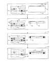
次に、以上述べた液体吐出素子の製造方法について説明する。図2には、本発明の第1の実施形態に係る液体吐出素子の製造工程をステップ図で示す。図中各欄の左図は図1(b)と同様の向きからみた液体吐出素子の平面図を、右図は左図のX−X線からみた断面図を示し、後述する図3〜5についても同様である。 Next, a method for manufacturing the liquid discharge element described above will be described. FIG. 2 is a step diagram showing the manufacturing process of the liquid ejection element according to the first embodiment of the present invention. The left figure of each column in the figure shows a plan view of the liquid ejection element viewed from the same direction as in FIG. 1B, the right figure shows a cross-sectional view seen from the line XX of the left figure, and will be described later with reference to FIGS. The same applies to.
(ステップ61)まず、625μm厚の基板11上にTaN膜およびAl膜をスパッタ法にて成膜し、フォトリソグラフィー技術を用いて発熱抵抗部16と電極15とを形成する。これらのプロセスは高温下でおこなわれるため、基板11は高温にさらされるが、十分に厚い層厚を有しているので、反りや破損が生じることはない。 (Step 61) First, a TaN film and an Al film are formed on a substrate 625 μm thick by sputtering, and the
(ステップ62)次に、バックグラインドで裏面3を切削し、基板11厚さを50〜300μm厚にする。必要に応じ、CMPやスピンエッチャーで破砕層を除去してもよい。薄化後の基板11の厚さは、貫通電極の貫通穴形成コストおよびインク供給口の形成コストや、薄化した後の基板の搬送等のハンドリング性から決定される。次に、貫通電極となる部分にドライエッチングによって、裏面3から内径70μmの貫通穴22を開ける。貫通穴22の形成方法はドライエッチングに限定されず、レーザ光や超音波加工等を用いることも可能である。貫通穴22の側面には、必要に応じて絶縁層(図示せず)を形成してもよい。なお、従来は、基板厚625μmのままでは貫通穴の形成の精度が悪く、その結果加工時間もかかるので、内径100μm程度が限界であったが、基板11を薄化したため内径を縮小することが可能となった。 (Step 62) Next, the back surface 3 is cut by back grinding so that the thickness of the
(ステップ63)次に、めっきシード層(図示せず)を成膜し、電解めっきによって貫通穴22に金めっきを充填して貫通電極12を形成する。 (Step 63) Next, a plating seed layer (not shown) is formed, and the through-
(ステップ64)次に、インク供給口形成のドライエッチング用マスク材を基板上に塗布し、フォトリソグラフィーでパターニングして、スリット状のインク供給口13をドライエッチングによって形成する。この段階で素子基板が完成する。 (Step 64) Next, a mask material for dry etching for forming an ink supply port is applied on the substrate and patterned by photolithography to form the slit-shaped
(ステップ65)最後に、樹脂のフィルムにレーザでオリフィス20を形成したオリフィスプレート21を基板に接着し、液体吐出素子が完成する。 (Step 65) Finally, the
以上説明した製造方法によって完成した液体吐出素子は、基板11の貫通穴22を短時間かつ高精度で加工できるので、低コストかつ高密度に貫通電極12が配置され、従来の液体吐出素子に比較して、チップ面積を小さくすることができる。また、インク供給口13の加工精度も向上するので、発熱抵抗部16とインク供給口13との間の寸法精度が向上し、周波数応答性がよくなり吐出性能が向上する。 Since the liquid discharge element completed by the manufacturing method described above can process the through
次に、図3を参照して、本発明の第2の実施形態に係る液体吐出素子の製造工程を説明する。本実施形態は、貫通電極の貫通穴とインク供給口のスリットとを同時に形成する点が第1の実施形態と異なる。以下、第1の実施形態との差異点を中心に説明する。 Next, with reference to FIG. 3, the manufacturing process of the liquid discharge element according to the second embodiment of the present invention will be described. This embodiment is different from the first embodiment in that the through hole of the through electrode and the slit of the ink supply port are formed simultaneously. Hereinafter, the difference from the first embodiment will be mainly described.
(ステップ71)ステップ61と同様にして発熱抵抗部16と電極15とを形成する。 (Step 71) The
(ステップ72)ステップ62と同様にして裏面3を切削し、基板11厚さを50〜300μm厚にする。また、ステップ62と同様にして内径70μmの貫通穴22を開ける。さらに、貫通穴22と同時に、ステップ64と同様にして、スリット状のインク供給口13をドライエッチングによって形成する。貫通穴22の側面には、必要に応じて絶縁層(図示せず)を形成してもよい(この際には、インク供給口13をドライフィルム等のフィルムでカバーする。)。このように、インク供給口13と貫通電極用の貫通穴22とが同時にエッチングできるので、製造効率の改善やコストダウンが可能となる。 (Step 72) The back surface 3 is cut in the same manner as in
(ステップ73)ステップ63と同様にして貫通穴22に金めっきを充填して貫通電極12を形成する。この段階で素子基板が完成する。 (Step 73) Similarly to step 63, the through
(ステップ74)次に、インク供給口形成部をカバーしているフィルムを設けた場合にはそれを除去し、ステップ65と同様にして、オリフィスプレート21を基板11に接着し、液体吐出素子が完成する。 (Step 74) Next, if a film covering the ink supply port forming portion is provided, it is removed, and the
本実施形態によれば、インク供給口の形成と貫通電極の貫通穴の形成が同時にできるので、加工コストの大幅な削減をすることが可能となる。 According to the present embodiment, since the ink supply port and the through hole of the through electrode can be formed at the same time, the processing cost can be greatly reduced.
次に、図4を参照して、本発明の第3の実施形態に係る液体吐出素子の製造工程を説明する。本実施形態は、オリフィスの高精度化および液流路と発熱抵抗体とのアライメント精度向上のために、オリフィスプレートを積層して形成する工程を有する点が、第1,2の実施形態と異なる。 Next, with reference to FIG. 4, the manufacturing process of the liquid discharge element according to the third embodiment of the present invention will be described. This embodiment is different from the first and second embodiments in that it has a step of stacking and forming an orifice plate in order to improve the accuracy of the orifice and improve the alignment accuracy between the liquid flow path and the heating resistor. .
(ステップ81〜83)ステップ61〜63と同様にして、発熱抵抗部16と電極15とを形成し、裏面3を薄化し、貫通穴22を開け、貫通電極12を形成する。 (Steps 81 to 83) In the same manner as in
(ステップ84)次に、液流路を形成するための型としてポジレジストを15μm厚で塗布し、露光、現像によって、所定のパターン26を形成する。 (Step 84) Next, a positive resist is applied in a thickness of 15 μm as a mold for forming the liquid flow path, and a
(ステップ85)次に、そして、オリフィスプレート21の材料として感光性のネガ型のエポキシ膜27を30μm厚で塗布し、露光、現像によって、内径25μmのオリフィス20の形成されたオリフィスプレート21を形成する。 (Step 85) Next, a photosensitive negative epoxy film 27 is applied as a material of the
(ステップ86)次に、その上に保護材として樹脂膜28を塗布する。 (Step 86) Next, a
(ステップ87)次に、ステップ64と同様にして裏面3にインク供給口13のスリットを形成する。 (Step 87) Next, the slit of the
(ステップ88)最後にオリフィスプレート21を保護していた樹脂膜28と液流路の型材であるパターン26とを除去し、液体吐出素子が完成する。パターン26の除去は、溶剤を基板11を浸漬したり、スプレーで吹き付けることによっておこなわれる。 (Step 88) Finally, the
本実施形態による製造方法によれば、オリフィスが精度よく形成され、液流路の製作精度も良好なので、発熱抵抗体とのアライメント精度も向上する。したがって、今後の小液滴化を図ったインクジェット記録にも十分に対応が可能であり、記録性能の向上につながる。 According to the manufacturing method according to the present embodiment, the orifice is formed with high accuracy and the manufacturing accuracy of the liquid flow path is also good, so that the alignment accuracy with the heating resistor is also improved. Accordingly, it is possible to sufficiently cope with future ink jet recording in which droplets are reduced, leading to improvement in recording performance.
次に、図5を参照して、本発明の第4の実施形態に係る液体吐出素子の製造工程を説明する。本実施形態も第3の実施形態と同様、オリフィスの高精度化および液流路と発熱抵抗体とのアライメント精度アップのために、オリフィスプレートを積層して形成する方法であるが、貫通電極の貫通穴とインク供給口の貫通穴とを同時に形成する点が第3の実施形態と異なる。 Next, with reference to FIG. 5, the manufacturing process of the liquid discharge element according to the fourth embodiment of the present invention will be described. As in the third embodiment, this embodiment is a method in which an orifice plate is laminated to increase the accuracy of the orifice and increase the alignment accuracy between the liquid flow path and the heating resistor. The difference from the third embodiment is that the through hole and the through hole of the ink supply port are formed simultaneously.
(ステップ91〜92)ステップ61と同様にして、発熱抵抗部16と電極15とを形成し、ステップ62と同様にして、裏面3を薄化する。 (Steps 91-92) The
(ステップ93〜95)次に、ステップ84〜86と同様にして、所定のパターン26を形成し、オリフィス20の形成されたオリフィスプレート21を形成し、その上に保護材として樹脂膜28を塗布する。 (Steps 93 to 95) Next, in the same manner as in
(ステップ96)次に、インク供給口形成13および貫通穴22のドライエッチング用マスク材を基板11上に塗布し、フォトリソグラフィーでパターニングして、インク供給口13のスリットおよび貫通穴22をドライエッチングによって同時に形成する。貫通穴22の側面には、必要に応じて絶縁層(図示せず)を形成してもよい(この際には、インク供給口13をドライフィルム等のフィルムでカバーする。)。 (Step 96) Next, a mask material for dry etching of the
(ステップ97)ステップ63と同様にして貫通穴22に金めっきを充填して貫通電極12を形成する。 (Step 97) Similarly to step 63, the through
(ステップ97)最後に、ステップ88と同様にして、インク供給口13をカバーしているフィルムを設けた場合にはそれを除去し、オリフィスプレート21を保護していた樹脂膜28と液流路14の型材であるパターン26とを除去し、液体吐出素子が完成する。 (Step 97) Finally, in the same manner as in
本実施形態によれば、オリフィスの加工精度や、液流路と発熱抵抗体とのアライメント精度の向上を図ることができるだけでなく、インク供給口の形成と貫通電極の貫通穴の形成とが同時にできるので、加工コストの大幅な削減をすることが可能となる。 According to the present embodiment, not only the processing accuracy of the orifice and the alignment accuracy between the liquid flow path and the heating resistor can be improved, but also the formation of the ink supply port and the formation of the through hole of the through electrode are performed simultaneously. Therefore, it is possible to greatly reduce the processing cost.
このように、本発明は、厚い基板の状態で高温プロセスを伴う発熱抵抗体および電極の形成をおこない、これによって高温による基板の反りや破損を防止し、次に基板の薄化をおこない、その後に薄い基板の状態でインク供給口および貫通電極形成用の貫通穴の形成をおこない、これによってこれらの穴の形成を高精度、高効率でおこなうことを特徴とするものである。したがって、かかる条件が満たされれば、上述したように貫通電極形成工程とインク供給口形成工程の順番は適宜に定めることができる。また、オリフィス形成工程と、貫通電極/インク供給口形成工程との順番も適宜に定めることができる。 In this way, the present invention forms a heating resistor and electrode with a high temperature process in a thick substrate state, thereby preventing the substrate from warping or breaking due to high temperature, and then thinning the substrate, In addition, the ink supply port and the through hole for forming the through electrode are formed in the state of a thin substrate, thereby forming these holes with high accuracy and high efficiency. Therefore, if this condition is satisfied, the order of the through electrode forming step and the ink supply port forming step can be determined as appropriate as described above. Further, the order of the orifice forming step and the through electrode / ink supply port forming step can be determined as appropriate.
本発明の効果は以下の通りである。基板上に発熱抵抗体と電極形成後基板を薄化する工程後に貫通電極およびインク供給口を形成することによって、基板の貫通穴を短時間に高精度で加工できるので、低コストで高密度に貫通電極を配置することができ、インク供給口の精度が向上する。また、発熱抵抗体とインク供給口との間の寸法のばらつきが減少するので吐出性能が向上する。更に、裏面のインク供給口の開口が小さくすることができ、それによって、チップを小さくでき、チップのコストダウンをすることができる。更に、インク供給口および貫通電極穴の形成を同時に行えるので、加工時間が半分になり加工コストの大幅な削減をすることができる。 The effects of the present invention are as follows. By forming the through-hole electrode and the ink supply port after the process of thinning the substrate after forming the heating resistor and electrode on the substrate, the through-hole of the substrate can be processed with high accuracy in a short time. The through electrode can be arranged, and the accuracy of the ink supply port is improved. Further, since the dimensional variation between the heating resistor and the ink supply port is reduced, the ejection performance is improved. Furthermore, the opening of the ink supply port on the back surface can be reduced, whereby the chip can be made smaller and the cost of the chip can be reduced. Furthermore, since the ink supply port and the through-electrode hole can be formed simultaneously, the processing time can be halved and the processing cost can be greatly reduced.
1 液体吐出素子
10 素子基板
11 基板
12 貫通電極
13 インク供給口
14 液流路
15 電極
16 発熱抵抗体
18 吐出口
20 オリフィス
21 オリフィスプレート
22 貫通穴
26 パターン
27 エポキシ膜
28 樹脂膜
100 記録ヘッドカートリッジ
101 インクタンク
102 インクホルダ
103 ベースプレート
104 記録ヘッドDESCRIPTION OF SYMBOLS 1
Claims (4)
Translated fromJapanese前記基板上に前記エネルギー供給手段を形成する工程と、
その後に、前記基板を薄化する工程と、
その後に、前記基板に前記インク供給口を形成するインク供給口形成工程と、
を有し、
前記素子基板は、前記基板を貫通して前記エネルギー供給手段に接続し、前記エネルギー供給手段に駆動電流を供給する貫通電極をさらに有し、
前記インク供給口形成工程は、前記基板に前記インク供給口と前記貫通電極とを形成する貫通部形成工程を有する、素子基板の形成方法。A method for forming an element substrate, comprising: a substrate; an ink supply port penetrating the substrate; and an energy supply unit provided on the substrate and configured to supply ejection energy to the ink flowing from the ink supply port,
Forming the energy supply means on the substrate;
Then, thinning the substrate,
Thereafter, an ink supply port forming step for forming the ink supply port on the substrate;
I have a,
The element substrate further includes a through electrode that penetrates the substrate and connects to the energy supply unit, and supplies a drive current to the energy supply unit.
Said ink supply port forming step, have a penetrating portion forming step of forming said through electrode and the ink supply port to said substrate, the element forming method of a substrate.
前記貫通電極の形成のための貫通穴を形成する工程と、
その後に、前記貫通穴に導電性材料を充填し前記貫通電極を形成する工程と、
その後に、前記インク供給口を形成する工程と、
を有する、
請求項1に記載の素子基板の形成方法。The penetration part forming step includes
Forming a through hole for forming the through electrode;
Thereafter, filling the through hole with a conductive material to form the through electrode;
Thereafter, the step of forming the ink supply port;
Having
The method for forming an element substrate according to claim1 .
前記インク供給口と、前記貫通電極の形成のための貫通穴とを同時に形成する工程と、
その後に、前記貫通穴に導電性材料を充填し前記貫通電極を形成する工程と、
を有する、
請求項1に記載の素子基板の形成方法。The penetration part forming step includes
Simultaneously forming the ink supply port and a through hole for forming the through electrode;
Thereafter, filling the through hole with a conductive material to form the through electrode;
Having
The method for forming an element substrate according to claim1 .
前記インク供給口と接続し、前記素子基板の前記エネルギー供給手段が設けられた面上を延びる液流路と、該液流路と接続し前記エネルギー供給手段によって吐出エネルギーを与えられたインクを記録媒体に吐出させるオリフィスとを形成するオリフィスプレートを形成する工程と、
を有する、液体吐出素子の形成方法。Forming a device substrate by the method of forming the element substrate according to any one of claims 1 to3,
A liquid flow path connected to the ink supply port and extending on the surface of the element substrate on which the energy supply means is provided, and ink connected to the liquid flow path and provided with ejection energy by the energy supply means is recorded. Forming an orifice plate for forming an orifice to be ejected to the medium;
A method for forming a liquid ejection element, comprising:
Priority Applications (5)
| Application Number | Priority Date | Filing Date | Title |
|---|---|---|---|
| JP2004210086AJP4274554B2 (en) | 2004-07-16 | 2004-07-16 | Element substrate and method for forming liquid ejection element |
| US11/179,543US7757397B2 (en) | 2004-07-16 | 2005-07-13 | Method for forming an element substrate |
| TW094124154ATWI273983B (en) | 2004-07-16 | 2005-07-15 | Liquid ejection element and manufacturing method therefor |
| KR1020050064023AKR100790605B1 (en) | 2004-07-16 | 2005-07-15 | Manufacturing Method of Device Substrate and Manufacturing Method of Liquid Discharge Device |
| CNB200510084876XACN100418773C (en) | 2004-07-16 | 2005-07-18 | Liquid ejection element and manufacturing method therefor |
Applications Claiming Priority (1)
| Application Number | Priority Date | Filing Date | Title |
|---|---|---|---|
| JP2004210086AJP4274554B2 (en) | 2004-07-16 | 2004-07-16 | Element substrate and method for forming liquid ejection element |
Publications (2)
| Publication Number | Publication Date |
|---|---|
| JP2006027108A JP2006027108A (en) | 2006-02-02 |
| JP4274554B2true JP4274554B2 (en) | 2009-06-10 |
Family
ID=35598986
Family Applications (1)
| Application Number | Title | Priority Date | Filing Date |
|---|---|---|---|
| JP2004210086AExpired - Fee RelatedJP4274554B2 (en) | 2004-07-16 | 2004-07-16 | Element substrate and method for forming liquid ejection element |
Country Status (5)
| Country | Link |
|---|---|
| US (1) | US7757397B2 (en) |
| JP (1) | JP4274554B2 (en) |
| KR (1) | KR100790605B1 (en) |
| CN (1) | CN100418773C (en) |
| TW (1) | TWI273983B (en) |
Families Citing this family (6)
| Publication number | Priority date | Publication date | Assignee | Title |
|---|---|---|---|---|
| JP4274555B2 (en)* | 2004-07-16 | 2009-06-10 | キヤノン株式会社 | Method for manufacturing liquid discharge element substrate and method for manufacturing liquid discharge element |
| JP4274556B2 (en)* | 2004-07-16 | 2009-06-10 | キヤノン株式会社 | Method for manufacturing liquid ejection element |
| JP4274554B2 (en) | 2004-07-16 | 2009-06-10 | キヤノン株式会社 | Element substrate and method for forming liquid ejection element |
| JP2008012911A (en)* | 2006-06-07 | 2008-01-24 | Canon Inc | Liquid discharge head and method of manufacturing liquid discharge head |
| JP5371475B2 (en)* | 2009-02-17 | 2013-12-18 | キヤノン株式会社 | Ink jet recording head and cleaning method thereof |
| US11161351B2 (en) | 2018-09-28 | 2021-11-02 | Canon Kabushiki Kaisha | Liquid ejection head |
Family Cites Families (34)
| Publication number | Priority date | Publication date | Assignee | Title |
|---|---|---|---|---|
| JPH0729431B2 (en)* | 1986-03-04 | 1995-04-05 | キヤノン株式会社 | How to make a liquid jet recording head |
| JPH0729433B2 (en)* | 1986-03-05 | 1995-04-05 | キヤノン株式会社 | How to make a liquid jet recording head |
| US4791440A (en)* | 1987-05-01 | 1988-12-13 | International Business Machine Corporation | Thermal drop-on-demand ink jet print head |
| JP2846636B2 (en)* | 1987-12-02 | 1999-01-13 | キヤノン株式会社 | Method of manufacturing substrate for inkjet recording head |
| AU657720B2 (en)* | 1991-01-30 | 1995-03-23 | Canon Kabushiki Kaisha | A bubblejet image reproducing apparatus |
| JP2960608B2 (en) | 1992-06-04 | 1999-10-12 | キヤノン株式会社 | Method for manufacturing liquid jet recording head |
| JP3143307B2 (en) | 1993-02-03 | 2001-03-07 | キヤノン株式会社 | Method of manufacturing ink jet recording head |
| US6190005B1 (en)* | 1993-11-19 | 2001-02-20 | Canon Kabushiki Kaisha | Method for manufacturing an ink jet head |
| JP3343875B2 (en) | 1995-06-30 | 2002-11-11 | キヤノン株式会社 | Method of manufacturing inkjet head |
| JPH0924612A (en) | 1995-07-11 | 1997-01-28 | Canon Inc | Inkjet head |
| US5994205A (en)* | 1997-02-03 | 1999-11-30 | Kabushiki Kaisha Toshiba | Method of separating semiconductor devices |
| JPH11320873A (en)* | 1997-06-05 | 1999-11-24 | Ricoh Co Ltd | Inkjet head |
| US6013534A (en)* | 1997-07-25 | 2000-01-11 | The United States Of America As Represented By The National Security Agency | Method of thinning integrated circuits received in die form |
| JP3726469B2 (en) | 1998-02-13 | 2005-12-14 | セイコーエプソン株式会社 | Method for manufacturing ink jet recording head |
| JP2000052549A (en)* | 1998-08-06 | 2000-02-22 | Ricoh Co Ltd | Actuator for inkjet head and inkjet head using the actuator |
| JP2000177122A (en) | 1998-12-14 | 2000-06-27 | Ricoh Co Ltd | Ink jet head and method of manufacturing the same |
| JP2000222711A (en)* | 1999-01-28 | 2000-08-11 | Alps Electric Co Ltd | Production of thin-film magnetic head and apparatus for production therefor |
| US6569343B1 (en)* | 1999-07-02 | 2003-05-27 | Canon Kabushiki Kaisha | Method for producing liquid discharge head, liquid discharge head, head cartridge, liquid discharging recording apparatus, method for producing silicon plate and silicon plate |
| JP2001171111A (en) | 1999-12-15 | 2001-06-26 | Seiko Epson Corp | Method of manufacturing inkjet head |
| JP2001315337A (en)* | 2000-05-01 | 2001-11-13 | Fuji Xerox Co Ltd | Ink jet recording head, ink jet recorder and method for manufacturing head |
| JP2001315370A (en)* | 2000-05-02 | 2001-11-13 | Fujita Masashi | Thermal printing head and its manufacturing method |
| JP2001322276A (en)* | 2000-05-15 | 2001-11-20 | Fuji Xerox Co Ltd | Ink jet recording head, ink jet recorder and method of making the head |
| KR20020009828A (en)* | 2000-07-27 | 2002-02-02 | 윤종용 | Forming method of via-hole in ink-jet print head |
| JP2002052709A (en)* | 2000-08-11 | 2002-02-19 | Hitachi Koki Co Ltd | Inkjet head housing structure |
| JP2002067328A (en) | 2000-08-28 | 2002-03-05 | Casio Comput Co Ltd | Recording head |
| JP2002301824A (en) | 2001-04-05 | 2002-10-15 | Fuji Xerox Co Ltd | Ink jet recording head, its manufacturing method, and ink jet recorder |
| JP4136523B2 (en)* | 2001-08-10 | 2008-08-20 | キヤノン株式会社 | Method for manufacturing liquid discharge head, substrate for liquid discharge head, and substrate processing method |
| CN1408550A (en)* | 2001-09-28 | 2003-04-09 | 飞赫科技股份有限公司 | Piezoelectric inkjet print head and manufacturing method thereof |
| US20040134881A1 (en)* | 2002-07-04 | 2004-07-15 | Seiko Epson Corporation | Method of manufacturing liquid jet head |
| US7381341B2 (en)* | 2002-07-04 | 2008-06-03 | Seiko Epson Corporation | Method of manufacturing liquid jet head |
| JP2004181651A (en) | 2002-11-29 | 2004-07-02 | Seiko Epson Corp | Method of manufacturing liquid discharge head, liquid discharge head, device manufacturing apparatus including the same, and ink jet recording apparatus |
| JP4274556B2 (en)* | 2004-07-16 | 2009-06-10 | キヤノン株式会社 | Method for manufacturing liquid ejection element |
| JP4274555B2 (en)* | 2004-07-16 | 2009-06-10 | キヤノン株式会社 | Method for manufacturing liquid discharge element substrate and method for manufacturing liquid discharge element |
| JP4274554B2 (en) | 2004-07-16 | 2009-06-10 | キヤノン株式会社 | Element substrate and method for forming liquid ejection element |
- 2004
- 2004-07-16JPJP2004210086Apatent/JP4274554B2/ennot_activeExpired - Fee Related
- 2005
- 2005-07-13USUS11/179,543patent/US7757397B2/ennot_activeExpired - Fee Related
- 2005-07-15TWTW094124154Apatent/TWI273983B/ennot_activeIP Right Cessation
- 2005-07-15KRKR1020050064023Apatent/KR100790605B1/ennot_activeExpired - Fee Related
- 2005-07-18CNCNB200510084876XApatent/CN100418773C/ennot_activeExpired - Fee Related
Also Published As
| Publication number | Publication date |
|---|---|
| JP2006027108A (en) | 2006-02-02 |
| TWI273983B (en) | 2007-02-21 |
| US20060012641A1 (en) | 2006-01-19 |
| CN1721189A (en) | 2006-01-18 |
| US7757397B2 (en) | 2010-07-20 |
| CN100418773C (en) | 2008-09-17 |
| KR20060050197A (en) | 2006-05-19 |
| KR100790605B1 (en) | 2008-01-02 |
| TW200607653A (en) | 2006-03-01 |
Similar Documents
| Publication | Publication Date | Title |
|---|---|---|
| JP4480182B2 (en) | Inkjet recording head substrate and method of manufacturing inkjet recording head | |
| JP5106601B2 (en) | Method for manufacturing liquid discharge head substrate, method for manufacturing liquid discharge head, and method for inspecting liquid discharge head substrate | |
| JP5762200B2 (en) | Manufacturing method of substrate for liquid discharge head | |
| KR20080033111A (en) | Manufacturing method of ink jet print head and ink jet print head | |
| US8191998B2 (en) | Liquid ejecting head | |
| JP4208794B2 (en) | Inkjet head substrate, method for producing the substrate, and inkjet head using the substrate | |
| US20080180486A1 (en) | Liquid ejection head and method for manufacturing liquid ejection head | |
| JP4208793B2 (en) | Inkjet head substrate, method for producing the substrate, and inkjet head using the substrate | |
| JP4274554B2 (en) | Element substrate and method for forming liquid ejection element | |
| JP2007229976A (en) | Inkjet head chip, inkjet head and method for manufacturing inkjet head chip | |
| CN100406259C (en) | Liquid ejection element and method of manufacturing the same | |
| US20100149280A1 (en) | Substrate for ink ejection heads, ink ejection head, method ofmanufacturing substrate, and method of manufacturing ink ejection head | |
| US8100508B2 (en) | Ink jet printing head | |
| JP2007290160A (en) | Liquid discharge head | |
| JP4274556B2 (en) | Method for manufacturing liquid ejection element | |
| JP5224782B2 (en) | Method for manufacturing liquid discharge head | |
| CN108136776A (en) | fluid ejection equipment | |
| JP2014046665A (en) | Method for manufacturing liquid discharge head | |
| JP3814608B2 (en) | Method for manufacturing ink jet recording head | |
| JP4671330B2 (en) | Method for manufacturing ink jet recording head | |
| JP2011062895A (en) | Inkjet head | |
| JP2024058748A (en) | Manufacturing method of liquid ejection head and liquid ejection head | |
| JP2002331665A (en) | Thermal inkjet head | |
| JP2006218735A (en) | Ink jet recording head and manufacturing method thereof | |
| JP2005059349A (en) | Inkjet recording head, method of manufacturing the same, inkjet recording cartridge, inkjet recorder, and method of manufacturing hollow structure body |
Legal Events
| Date | Code | Title | Description |
|---|---|---|---|
| A621 | Written request for application examination | Free format text:JAPANESE INTERMEDIATE CODE: A621 Effective date:20051212 | |
| A977 | Report on retrieval | Free format text:JAPANESE INTERMEDIATE CODE: A971007 Effective date:20081001 | |
| A131 | Notification of reasons for refusal | Free format text:JAPANESE INTERMEDIATE CODE: A131 Effective date:20081022 | |
| A521 | Request for written amendment filed | Free format text:JAPANESE INTERMEDIATE CODE: A523 Effective date:20081218 | |
| TRDD | Decision of grant or rejection written | ||
| A01 | Written decision to grant a patent or to grant a registration (utility model) | Free format text:JAPANESE INTERMEDIATE CODE: A01 Effective date:20090225 | |
| A01 | Written decision to grant a patent or to grant a registration (utility model) | Free format text:JAPANESE INTERMEDIATE CODE: A01 | |
| A61 | First payment of annual fees (during grant procedure) | Free format text:JAPANESE INTERMEDIATE CODE: A61 Effective date:20090302 | |
| R150 | Certificate of patent or registration of utility model | Ref document number:4274554 Country of ref document:JP Free format text:JAPANESE INTERMEDIATE CODE: R150 Free format text:JAPANESE INTERMEDIATE CODE: R150 | |
| FPAY | Renewal fee payment (event date is renewal date of database) | Free format text:PAYMENT UNTIL: 20120313 Year of fee payment:3 | |
| FPAY | Renewal fee payment (event date is renewal date of database) | Free format text:PAYMENT UNTIL: 20130313 Year of fee payment:4 | |
| FPAY | Renewal fee payment (event date is renewal date of database) | Free format text:PAYMENT UNTIL: 20140313 Year of fee payment:5 | |
| LAPS | Cancellation because of no payment of annual fees |