JP4273975B2 - Method for producing flexible polymer optical waveguide - Google Patents
Method for producing flexible polymer optical waveguideDownload PDFInfo
- Publication number
- JP4273975B2 JP4273975B2JP2004009427AJP2004009427AJP4273975B2JP 4273975 B2JP4273975 B2JP 4273975B2JP 2004009427 AJP2004009427 AJP 2004009427AJP 2004009427 AJP2004009427 AJP 2004009427AJP 4273975 B2JP4273975 B2JP 4273975B2
- Authority
- JP
- Japan
- Prior art keywords
- optical waveguide
- curable resin
- mold
- polymer optical
- core
- Prior art date
- Legal status (The legal status is an assumption and is not a legal conclusion. Google has not performed a legal analysis and makes no representation as to the accuracy of the status listed.)
- Expired - Fee Related
Links
- 230000003287optical effectEffects0.000titleclaimsdescription140
- 238000004519manufacturing processMethods0.000titleclaimsdescription87
- 229920005570flexible polymerPolymers0.000titleclaimsdescription44
- 229920005989resinPolymers0.000claimsdescription188
- 239000011347resinSubstances0.000claimsdescription188
- 239000000758substrateSubstances0.000claimsdescription86
- 229920000642polymerPolymers0.000claimsdescription84
- 238000000034methodMethods0.000claimsdescription63
- 239000000463materialSubstances0.000claimsdescription38
- 238000005253claddingMethods0.000claimsdescription28
- 239000007788liquidSubstances0.000claimsdescription19
- 230000008569processEffects0.000claimsdescription16
- 238000011049fillingMethods0.000claimsdescription14
- 239000011521glassSubstances0.000claimsdescription14
- 125000002723alicyclic groupChemical group0.000claimsdescription10
- -1polydimethylsiloxanePolymers0.000claimsdescription10
- 230000015572biosynthetic processEffects0.000claimsdescription9
- 229920001971elastomerPolymers0.000claimsdescription8
- 229920005672polyolefin resinPolymers0.000claimsdescription8
- 239000005060rubberSubstances0.000claimsdescription8
- 239000004205dimethyl polysiloxaneSubstances0.000claimsdescription7
- 229920000435poly(dimethylsiloxane)Polymers0.000claimsdescription7
- 230000000149penetrating effectEffects0.000claimsdescription6
- 125000003518norbornenyl groupChemical groupC12(C=CC(CC1)C2)*0.000claimsdescription5
- 230000003746surface roughnessEffects0.000claimsdescription4
- 239000002985plastic filmSubstances0.000claims1
- 229920006255plastic filmPolymers0.000claims1
- 239000010410layerSubstances0.000description78
- 239000000178monomerSubstances0.000description12
- 229920002379silicone rubberPolymers0.000description12
- 125000006850spacer groupChemical group0.000description9
- 229920001187thermosetting polymerPolymers0.000description9
- 230000008859changeEffects0.000description8
- 230000005540biological transmissionEffects0.000description6
- 239000004944Liquid Silicone RubberSubstances0.000description5
- 239000003795chemical substances by applicationSubstances0.000description5
- 239000012792core layerSubstances0.000description5
- 238000005516engineering processMethods0.000description5
- 239000004945silicone rubberSubstances0.000description5
- 239000011248coating agentSubstances0.000description4
- 238000000576coating methodMethods0.000description4
- 239000002184metalSubstances0.000description4
- 239000000203mixtureSubstances0.000description4
- 239000013307optical fiberSubstances0.000description4
- 229920001296polysiloxanePolymers0.000description4
- 239000004593EpoxySubstances0.000description3
- YCKRFDGAMUMZLT-UHFFFAOYSA-NFluorine atomChemical compound[F]YCKRFDGAMUMZLT-UHFFFAOYSA-N0.000description3
- 230000002411adverseEffects0.000description3
- 125000004453alkoxycarbonyl groupChemical group0.000description3
- 125000000217alkyl groupChemical group0.000description3
- 238000007796conventional methodMethods0.000description3
- 238000010586diagramMethods0.000description3
- 229910052731fluorineInorganic materials0.000description3
- 239000011737fluorineSubstances0.000description3
- 238000001053micromouldingMethods0.000description3
- 239000002086nanomaterialSubstances0.000description3
- 230000035515penetrationEffects0.000description3
- 238000000206photolithographyMethods0.000description3
- 239000000047productSubstances0.000description3
- 238000004080punchingMethods0.000description3
- 239000002904solventSubstances0.000description3
- 238000002834transmittanceMethods0.000description3
- 239000004925Acrylic resinSubstances0.000description2
- 229920000178Acrylic resinPolymers0.000description2
- CERQOIWHTDAKMF-UHFFFAOYSA-NMethacrylic acidChemical compoundCC(=C)C(O)=OCERQOIWHTDAKMF-UHFFFAOYSA-N0.000description2
- 239000004642PolyimideSubstances0.000description2
- NIXOWILDQLNWCW-UHFFFAOYSA-Nacrylic acid groupChemical groupC(C=C)(=O)ONIXOWILDQLNWCW-UHFFFAOYSA-N0.000description2
- 238000011161developmentMethods0.000description2
- 238000010438heat treatmentMethods0.000description2
- 230000001678irradiating effectEffects0.000description2
- 238000002156mixingMethods0.000description2
- 238000001020plasma etchingMethods0.000description2
- 239000004033plasticSubstances0.000description2
- 229920003023plasticPolymers0.000description2
- 229920001721polyimidePolymers0.000description2
- 238000006116polymerization reactionMethods0.000description2
- 239000002243precursorSubstances0.000description2
- 230000009467reductionEffects0.000description2
- 238000007789sealingMethods0.000description2
- 238000002174soft lithographyMethods0.000description2
- 239000000243solutionSubstances0.000description2
- 238000004528spin coatingMethods0.000description2
- XLYOFNOQVPJJNP-UHFFFAOYSA-NwaterSubstancesOXLYOFNOQVPJJNP-UHFFFAOYSA-N0.000description2
- ROLAGNYPWIVYTG-UHFFFAOYSA-N1,2-bis(4-methoxyphenyl)ethanamine;hydrochlorideChemical compoundCl.C1=CC(OC)=CC=C1CC(N)C1=CC=C(OC)C=C1ROLAGNYPWIVYTG-UHFFFAOYSA-N0.000description1
- 229920002284Cellulose triacetatePolymers0.000description1
- 239000004696Poly ether ether ketoneSubstances0.000description1
- 239000004695Polyether sulfoneSubstances0.000description1
- XUIMIQQOPSSXEZ-UHFFFAOYSA-NSiliconChemical compound[Si]XUIMIQQOPSSXEZ-UHFFFAOYSA-N0.000description1
- NNLVGZFZQQXQNW-ADJNRHBOSA-N[(2r,3r,4s,5r,6s)-4,5-diacetyloxy-3-[(2s,3r,4s,5r,6r)-3,4,5-triacetyloxy-6-(acetyloxymethyl)oxan-2-yl]oxy-6-[(2r,3r,4s,5r,6s)-4,5,6-triacetyloxy-2-(acetyloxymethyl)oxan-3-yl]oxyoxan-2-yl]methyl acetateChemical compoundO([C@@H]1O[C@@H]([C@H]([C@H](OC(C)=O)[C@H]1OC(C)=O)O[C@H]1[C@@H]([C@@H](OC(C)=O)[C@H](OC(C)=O)[C@@H](COC(C)=O)O1)OC(C)=O)COC(=O)C)[C@@H]1[C@@H](COC(C)=O)O[C@@H](OC(C)=O)[C@H](OC(C)=O)[C@H]1OC(C)=ONNLVGZFZQQXQNW-ADJNRHBOSA-N0.000description1
- 238000010521absorption reactionMethods0.000description1
- 239000000654additiveSubstances0.000description1
- 230000001070adhesive effectEffects0.000description1
- 230000008901benefitEffects0.000description1
- 238000004061bleachingMethods0.000description1
- 239000006227byproductSubstances0.000description1
- 125000004432carbon atomChemical groupC*0.000description1
- 238000005266castingMethods0.000description1
- 239000011247coating layerSubstances0.000description1
- 238000004891communicationMethods0.000description1
- 238000001035dryingMethods0.000description1
- 230000000694effectsEffects0.000description1
- 238000009429electrical wiringMethods0.000description1
- 238000004070electrodepositionMethods0.000description1
- 238000010894electron beam technologyMethods0.000description1
- 150000002148estersChemical group0.000description1
- 239000012467final productSubstances0.000description1
- 229920002457flexible plasticPolymers0.000description1
- 230000009477glass transitionEffects0.000description1
- 238000001746injection mouldingMethods0.000description1
- 230000010354integrationEffects0.000description1
- 238000003475laminationMethods0.000description1
- 238000001459lithographyMethods0.000description1
- 238000011068loading methodMethods0.000description1
- 238000012423maintenanceMethods0.000description1
- JFNLZVQOOSMTJK-KNVOCYPGSA-NnorborneneChemical compoundC1[C@@H]2CC[C@H]1C=C2JFNLZVQOOSMTJK-KNVOCYPGSA-N0.000description1
- 238000002256photodepositionMethods0.000description1
- 229920006393polyether sulfonePolymers0.000description1
- 229920002530polyetherether ketonePolymers0.000description1
- 239000002861polymer materialSubstances0.000description1
- 229920000307polymer substratePolymers0.000description1
- 238000002360preparation methodMethods0.000description1
- 238000003672processing methodMethods0.000description1
- 230000005855radiationEffects0.000description1
- 230000001105regulatory effectEffects0.000description1
- 238000011160researchMethods0.000description1
- 230000004044responseEffects0.000description1
- 239000004065semiconductorSubstances0.000description1
- 229910052710siliconInorganic materials0.000description1
- 239000010703siliconSubstances0.000description1
- 229920002050silicone resinPolymers0.000description1
- 229910001220stainless steelInorganic materials0.000description1
- 239000010935stainless steelSubstances0.000description1
- 238000009281ultraviolet germicidal irradiationMethods0.000description1
Images


Landscapes
- Optical Integrated Circuits (AREA)
Description
Translated fromJapanese本発明は、高分子光導波路の製造方法に関し、特に、薄いフレキシブルなフィルム状の高分子光導波路に関する。 The present invention relates to a method for producing a polymer optical waveguide, and more particularly to a thin flexible film-shaped polymer optical waveguide.
高分子導波路の製造方法としては、(1)フイルムにモノマーを含浸させてコア部を選択的に露光して屈折率を変化させフイルムを張り合わせる方法(選択重合法)、(2)コア層及びクラッド層を塗布後、反応性イオンエチングを用いてクラッド部を形成する方法(RIE法)、(3)高分子材料中に感光性の材料を添加した紫外線硬化樹脂を用いて、露光・現像するフォトリソグラフィー法を用いる方法(直接露光法)、(4)射出成形を利用する方法、(5)コア層及びクラッド層を塗布後、コア部を露光してコア部の屈折率を変化させる方法(フォトブリーチング法)等が提案されている。
しかし、(1)の選択重合法はフイルムの張り合わせに問題があり、(2)や(3)の方法は、フォトリソグラフィー法を使うためコスト高になり、(4)の方法は、得られるコア径の精度に課題がある。また、(5)の方法はコア層とクラッド層との十分な屈折率差がとれないという問題がある。
現在、性能的に優れた実用的な方法は、(2)や(3)の方法だけであるが前記のごときコストの問題がある。そして(1)ないし(5)のいずれの方法も、大面積でフレキシブルなプラスチック基材に高分子導波路を形成するのに適用しうるものではない。The polymer waveguide manufacturing method includes (1) a method of impregnating a film with a monomer and selectively exposing the core portion to change the refractive index to bond the films (selective polymerization method), and (2) a core layer. And a method of forming a cladding portion using reactive ion etching after applying the cladding layer (RIE method), and (3) exposure and development using an ultraviolet curable resin in which a photosensitive material is added to a polymer material. A method using a photolithography method (direct exposure method), (4) a method using injection molding, (5) a method of changing the refractive index of the core portion by exposing the core portion after applying the core layer and the clad layer ( Photo bleaching method) has been proposed.
However, the selective polymerization method (1) has a problem in film lamination, and the methods (2) and (3) are expensive because the photolithographic method is used. There is a problem in the accuracy of the diameter. Further, the method (5) has a problem that a sufficient refractive index difference between the core layer and the clad layer cannot be obtained.
At present, the practical methods excellent in performance are only the methods (2) and (3), but there is a problem of cost as described above. None of the methods (1) to (5) can be applied to form a polymer waveguide on a flexible plastic substrate having a large area.
また、高分子光導波路を製造する方法として、キャピラリーとなる溝のパターンが形成されたパターン基板(クラッド)にコア用のポリマー前駆体材料を充填し、その後硬化させてコア層を作り、その上に平面基板(クラッド)を貼り合わせる方法が知られているが、この方法ではキャピラリー溝にだけでなく、パターン基板と平面基板の間にも全面的にポリマー前駆体材料が薄く充填され硬化されて、コア層と同じ組成の薄い層が形成される結果、この薄い層を通って光が漏洩してしまうという問題があった。
この問題を解決する方法の1つとして、デビット・ハートはキャピラリーとなる溝のパターンが形成されたパターン基板と平面基板とをクランプ用治具で固着し、さらにパターン基板と平面基板との接触部分を樹脂でシールなどした後減圧して、モノマー(ジアリルイソフタレート)溶液をキャピラリーに充填して、高分子光導波路を製造する方法を提案した(以下の特許文献1を参照)。この方法はコア形成用樹脂材料としてポリマー前駆体材料を用いる代わりにモノマーを用いて充填材料を低粘度化し、キャピラリー内に毛細管現象を利用して充填させ、キャピラリー以外にはモノマーが充填されないようにする方法である。
しかし、この方法はコア形成用材料としてモノマーを用いているため、モノマーが重合してポリマーになる際の体積収縮率が大きく、高分子光導波路の透過損失が大きくなるいう問題がある。また、この方法は、パターン基板と平面基板とをクランプで固着する、あるいはこれに加えさらに接触部を樹脂でシールするなど煩雑な方法であり、量産にはむかず、その結果コスト低下を期待することはできない。また、クラッドとして厚さがmmオーダーあるいは1mm以下のフィルムを用いる高分子光導波路の製造に適用することは不可能である。In addition, as a method of manufacturing a polymer optical waveguide, a core substrate is formed by filling a polymer substrate material for a core into a pattern substrate (cladding) on which a groove pattern serving as a capillary is formed, and then curing the core layer. In this method, the polymer precursor material is thinly filled and cured not only in the capillary groove but also between the pattern substrate and the flat substrate. As a result of the formation of a thin layer having the same composition as the core layer, there is a problem that light leaks through the thin layer.
As one method for solving this problem, Debit Hart uses a clamping jig to fix the pattern substrate on which a groove pattern serving as a capillary is formed and a flat substrate, and further, the contact portion between the pattern substrate and the flat substrate. A method of manufacturing a polymer optical waveguide by sealing the resin with a resin and then reducing the pressure and filling a capillary with a monomer (diallyl isophthalate) solution was proposed (see Patent Document 1 below). In this method, instead of using the polymer precursor material as the core forming resin material, the viscosity of the filling material is reduced by using a monomer, and the capillary is filled using the capillary phenomenon so that the monomer is not filled except the capillary. It is a method to do.
However, since this method uses a monomer as the core forming material, there is a problem that the volumetric shrinkage when the monomer is polymerized to become a polymer is large, and the transmission loss of the polymer optical waveguide is increased. In addition, this method is a complicated method such as fixing the pattern substrate and the flat substrate with a clamp, or additionally sealing the contact portion with resin, so that it is not suitable for mass production, and as a result, cost reduction is expected. I can't. Further, it cannot be applied to the production of a polymer optical waveguide using a film having a thickness of mm order or 1 mm or less as a clad.
また、最近、ハーバード大学のGeorge M. Whitesidesらは、ナノ構造を作る新技術として、ソフトリソグラフィーの一つとして毛細管マイクロモールドという方法を提唱している。これは、フォトリソグラフィーを利用してマスター基板を作り、ポリジメチルシロキサン(PDMS)の密着性と容易な剥離性を利用してマスター基板のナノ構造をPDMSの鋳型に写し取り、この鋳型に毛細管現象を利用して液体ポリマーを流し込んで固化させる方法である。以下の非特許文献1には詳しい解説記事が記載されている。 Recently, George M. Whitesides and others at Harvard University have proposed a method called capillary micromolding as one of the soft lithography as a new technology for creating nanostructures. This is because a master substrate is made using photolithography, and the nanostructure of the master substrate is copied to a PDMS mold using the adhesion and easy peelability of polydimethylsiloxane (PDMS). This is a method of pouring and solidifying a liquid polymer. The following non-patent document 1 describes detailed explanation articles.
また、ハーバード大学のGeorge M. WhitesidesのグループのKim Enochらによって毛細管マイクロモールド法に関する特許が出願されている(以下の特許文献2を参照)。しかし、この特許に記載の製造方法を高分子光導波路の製造に適用しても、光導波路のコア部は断面積が小さいので、コア部を形成するのに時間がかかり、量産に適さない。また、モノマー溶液が重合して高分子になるときに体積変化を起こしコアの形状が変化し、透過損失が大きくなるという欠点をもつ。 A patent on capillary micromolding has been filed by Kim Enoch et al. Of George M. Whitesides group at Harvard University (see Patent Document 2 below). However, even if the manufacturing method described in this patent is applied to the manufacture of a polymer optical waveguide, the core portion of the optical waveguide has a small cross-sectional area, so that it takes time to form the core portion and is not suitable for mass production. In addition, when the monomer solution is polymerized into a polymer, the volume is changed, the core shape is changed, and the transmission loss is increased.
また、IBMチュリッヒ研究所のB. MichelらはPDMSを用いた高解像度のリソグラフィー技術を提案しており、この技術により数十nmの解像力が得られると報告している。詳しい解説記事は、以下の非特許文献2に記載されている。
このように、PDMSを使ったソフトリソグラフィー技術や、毛細管マイクロモールド法は、ナノテクノロジーとして最近、米国を中心に注目を集めている技術であるB. Michel et al. Of the IBM Zurich Research Institute have proposed a high-resolution lithography technique using PDMS, and reported that this technique can achieve a resolution of several tens of nanometers. Detailed commentary articles are described in Non-Patent Document 2 below.
In this way, soft lithography technology using PDMS and capillary micromolding are technologies that have recently attracted attention as nanotechnology mainly in the United States.
しかしながら、前記のごときマイクロモールド法を用いて光導波路を作製すると、硬化時の体積収縮率を小さくする(したがって透過損失を小さくする)ことと、充填を容易にするために充填液体(モノマー等)を低粘度化することを両立させえない。したがって、透過損失を小さくすることを優先的に考慮すると、充填液体の粘度をある限度以下にすることができず、充填速度が遅くなり、量産は望めない。また前記のマイクロモールド法は、基板としてガラスやシリコン基板を用いることが前提になっており、フレキシブルなフィルム基材を用いることは考慮されていない。 However, when an optical waveguide is manufactured by using the micromold method as described above, the volume shrinkage during curing is reduced (thus, transmission loss is reduced), and a filling liquid (monomer or the like) is used to facilitate filling. It is impossible to achieve a low viscosity. Therefore, if priority is given to reducing the transmission loss, the viscosity of the filling liquid cannot be reduced below a certain limit, the filling speed becomes slow, and mass production cannot be expected. The micromold method is based on the premise that a glass or silicon substrate is used as the substrate, and does not consider the use of a flexible film substrate.
一方、下記の特許文献3には、高分子光導波路を、剛性の低い型を用いることにより作製する方法が示されている。この方法は、第1の凹型から第2の凸型を作製し、第2の凸型に樹脂を塗布硬化させてコアパターンとなる凹部を有する第1のクラッドを形成し、第2の凸型を剥離した後、コアパターンとなる凹部に樹脂を塗布硬化させてコアを形成し、その後、さらに樹脂を塗布硬化させて第2クラッドを形成する方法であるが、凹部だけにコア用樹脂を充填することは難しく、微細なコアパターンを精度高く作製することは困難である。 On the other hand, Patent Document 3 below shows a method for producing a polymer optical waveguide by using a mold having low rigidity. In this method, a second convex mold is produced from the first concave mold, a resin is applied to the second convex mold and cured to form a first clad having a concave portion that becomes a core pattern, and the second convex mold. After the film is peeled off, the core is formed by coating and curing the resin in the recesses that will become the core pattern, and then the resin is further coated and cured to form the second cladding. It is difficult to make a fine core pattern with high accuracy.
ところで、最近、IC技術やLSI技術において、動作速度や集積度向上のために、高密度に電気配線を行なう代わりに、機器装置間、機器装置内のボード間、チップ内において光配線を行なうことが注目されている。
光配線のための素子として、例えば、光ファイバーをシート状のボードに布線した光ファイバー布線ボードが実用化されている。しかし、光ファイバーは端面の研磨が必要で接続のための光コネクタも高価である。By the way, recently, in IC technology and LSI technology, in order to improve the operation speed and the degree of integration, instead of performing high-density electrical wiring, optical wiring is performed between equipment devices, between boards in equipment equipment, and in chips. Is attracting attention.
As an element for optical wiring, for example, an optical fiber wiring board in which an optical fiber is wired on a sheet-like board has been put into practical use. However, the end face of the optical fiber needs to be polished, and the optical connector for connection is also expensive.
このようなことから、光ファイバーを高分子導波路に置き換えて低コスト化をはかることが求められている。また、フイルムの特性を生かしてフレキシブルな高分子導波路を作ることが求められている。しかし、一般にフレキシブルにするためにはフイルムを薄くする必要があるが、薄いと取扱が難しく高精度の加工方法である半導体プロセスを使うことができない。 For this reason, it is required to reduce the cost by replacing the optical fiber with a polymer waveguide. Also, it is required to make a flexible polymer waveguide by taking advantage of the characteristics of the film. However, it is generally necessary to make the film thin in order to make it flexible, but if it is thin, it is difficult to handle and a semiconductor process, which is a high-precision processing method, cannot be used.
本発明者らは、このような要請に対し、特願2003−58871号や特願2003−58872号等においてフレキシブルなフィルム状の高分子光導波路を非常に簡便な方法で製造する方法を提案した。この方法は、従来用いられていた高分子光導波路の製造方法に比較して、非常に安価であるにもかかわらず、導波損失の低い高分子光導波路を極めて低価格で提供できる方法であるが、クラッド用硬化性樹脂を塗布・硬化させて上部クラッド層を作ると、樹脂の硬化による体積収縮に伴い、フィルム状の高分子光導波路が反るなどの変形を起こすことがあった。
本発明は、前記のごとき問題点に鑑みてなされたものであり、その目的は、極めて低コストで単純化された簡便な方法により、反るなどの変形を生じない、フレキシブルな高分子光導波路を製造する方法を提供することにある。 The present invention has been made in view of the above problems, and its object is to provide a flexible polymer optical waveguide that does not undergo deformation such as warping by a simple method that is simplified at a very low cost. It is in providing the method of manufacturing.
(1)1)鋳型形成用硬化性樹脂の硬化層から形成され、かつ、光導波路コア凸部に対応する凹部と、該凹部の一端及び他端にそれぞれ連通する貫通孔が2つ設けられ、前記2つの貫通孔の1つは凹部の一端に連通する液だめのための貫通孔であり、前記2つの貫通孔のもう1つは凹部の他端に連通する減圧吸引のための貫通孔であり、前記液だめのための貫通孔及び減圧吸引のための貫通孔が、鋳型の凹部が形成された面及び前記面に対向する面を貫通する孔である鋳型を準備する工程、2)前記鋳型に該鋳型との密着性が良好な、クラッドとなるフレキシブルフィルム基材を密着させる工程、3)前記フレキシブルフィルム基材を密着させた鋳型の凹部の一端にある前記貫通孔に、コア形成用硬化性樹脂を充填し、鋳型の凹部の他端にある前記貫通孔から減圧吸引してコア形成用硬化性樹脂を前記鋳型の凹部に充填する工程、4)充填したコア形成用硬化性樹脂を硬化させる工程、5)鋳型を前記フレキシブルフィルム基材から剥離する工程、6)コアが形成された前記フレキシブルフィルム基材と表面に離型層を有する形状保持部材との間にクラッド用硬化性樹脂の層を設ける工程、7)クラッド用硬化性樹脂の層を硬化させる工程、及び8)前記形状保持部材をクラッド用硬化性樹脂の硬化層から剥離する工程、を有するフレキシブル高分子光導波路の製造方法。(1) 1) is formed from a cured layer of the curable resin mold formation, and the recesses corresponding to the optical waveguide core protrusions, through holes respectively communicating with the one end and the other end of the recesstwo provided,One of the two through-holes is a through-hole for reservoir that communicates with one end of the recess, and the other of the two through-holes is a through-hole for vacuum suction that communicates with the other end of the recess. And a step of preparing a mold in whichthe through hole for the reservoir and the through hole for vacuum suction are a hole penetrating the surface on which the concave portion of the mold is formed and the surface facing the surface , 2) mold is good adhesion with thetemplate, the step of adhering theflexible film substratemade of a clad, 3) inthe through hole at one end of the recess ofthe mold are brought into close contact withthe flexible film substrate, the core forming Fill with curable resin and place it at the other end of the Filling the core-forming curable resin in the recess of the mold by vacuum suction fromthe through-hole, 4) curing the filled core forming curable resin, 5) peeling the mold fromthe flexible film substrate 6) a step of providing a clad curable resin layer between theflexible film substrate on which the core is formed and a shape holding member having a release layer on the surface, 7) a clad curable resin layer step curing the, and 8) the method of producinga flexible polymer optical waveguide having a step, of removing the shape-retaining member from the cured layer of curable resin for cladding.
(2)前記形状保持部材が、ガラス板又は光透過性フィルムからなることを特徴とする、前記(1)に記載のフレキシブル高分子光導波路の製造方法。
(3)前記形状部材の厚さが150μm以上であることを特徴とする、前記(1)に記載のフレキシブル高分子光導波路の製造方法。
(4)前記離型層が、フッ素樹脂であることを特徴とする、前記(1)に記載のフレキシブル高分子光導波路の製造方法。
(5)前記フッ素樹脂がアモルファスフッ素樹脂であることを特徴とする、前記(4)に記載のフレキシブル高分子光導波路の製造方法。
(6)前記6)の工程において、コアが形成された前記フレキシブルフィルム基材と表面に離型層を有する形状保持部材との間に、クラッド用硬化性樹脂の層の厚さを規制するためのギャップ形成部材を用いることを特徴とする、前記(1)に記載のフレキシブル高分子光導波路の製造方法。(2) The method for producing aflexible polymer optical waveguide according to (1), wherein the shape holding member is made of a glass plate or a light transmissive film.
(3) The method for producing aflexible polymer optical waveguide according to (1), wherein the shape member has a thickness of 150 μm or more.
(4) The method for producing aflexible polymer optical waveguide according to (1), wherein the release layer is a fluororesin.
(5) The method for producing aflexible polymer optical waveguide according to (4), wherein the fluororesin is an amorphous fluororesin.
(6) In order to regulate the thicknessof the clad curable resin layerbetween the flexible film substrate on which the core is formed and the shape holding member having a release layer on the surface in the step 6) The method for producing aflexible polymer optical waveguide according to (1), wherein the gap forming member is used.
(7)前記鋳型形成用硬化性樹脂が、硬化性ポリジメチルシロキサンゴムであることを特徴とする、前記(1)に記載のフレキシブル高分子光導波路の製造方法。
(8)前記鋳型の表面粗さが100nm以下であることを特徴とする前記(1)に記載のフレキシブル高分子光導波路の製造方法。
(9)前記フレキシブルフィルム基材の屈折率が1.55以下であることを特徴とする、前記(1)に記載のフレキシブル高分子光導波路の製造方法。(7) The method for producing aflexible polymer optical waveguide according to (1) above, wherein the mold-forming curable resin is a curable polydimethylsiloxane rubber.
(8) The method for producing aflexible polymer optical waveguide according to (1), wherein the mold has a surface roughness of 100 nm or less.
(9) The method for producing aflexible polymer optical waveguide according to (1), wherein the refractive index of theflexible film substrate is 1.55 or less.
(10)前記フレキシブルフィルム基材が脂環式オレフィン樹脂フイルムであることを特徴とする、前記(1)に記載のフレキシブル高分子光導波路の製造方法。
(11)前記脂環式オレフィン樹脂フイルムが、主鎖にノルボルネン構造を有しかつ側鎖に極性基をもつ樹脂フィルムであることを特徴とする、前記(10)に記載のフレキシブル高分子光導波路の製造方法。
(12)前記コア形成用硬化性樹脂及びクラッド用硬化性樹脂が紫外線硬化型であることを特徴とする、前記(1)に記載のフレキシブル高分子光導波路の製造方法。
(13)前記コア形成用硬化性樹脂とクラッド用硬化性樹脂との硬化後の屈折率の差が0.01以上あることを特徴とする、前記(1)に記載のフレキシブル高分子光導波路の製造方法。
(14)前記コア形成用硬化性樹脂及びクラッド用硬化性樹脂の硬化収縮率が10%以下であることを特徴とする、前記(1)に記載のフレキシブル高分子光導波路の製造方法。
(15)前記コア形成用硬化性樹脂及びクラッド用硬化性樹脂の粘度が2000mP・s以下であることを特徴とする、前記(1)に記載のフレキシブル高分子光導波路の製造方法。
(16)前記高分子光導波路が、厚さ300μm以下のフィルム状高分子光導波路であることを特徴とする、前記(1)に記載のフレキシブル高分子光導波路の製造方法。(10) The method for producing aflexible polymer optical waveguide according to (1), wherein theflexible film substrate is an alicyclic olefin resin film.
(11) Theflexible polymer optical waveguide according to (10), wherein the alicyclic olefin resin film is a resin film having a norbornene structure in the main chain and a polar group in the side chain. Manufacturing method.
(12) The method for producing aflexible polymer optical waveguide according to (1), wherein the curable resin for core formation and the curable resin for clad are of an ultraviolet curable type.
(13) Theflexible polymer optical waveguide according to (1), wherein a difference in refractive index after curing between the core-forming curable resin and the clad curable resin is 0.01 or more. Production method.
(14) The method for producing aflexible polymer optical waveguide according to (1), wherein the curing shrinkage of the curable resin for core formation and the curable resin for clad is 10% or less.
(15) The method for producing aflexible polymer optical waveguide according to (1) above, wherein the viscosity of the curable resin for core formation and the curable resin for cladding is 2000 mP · s or less.
(16) The method for producing aflexible polymer optical waveguide according to (1), wherein the polymer optical waveguide is a film-shaped polymer optical waveguide having a thickness of 300 μm or less.
(17)1)鋳型形成用硬化性樹脂の硬化層から形成され、かつ、光導波路コア凸部に対応する凹部と、該凹部の一端及び他端にそれぞれ連通する貫通孔が2つ設けられ、前記2つの貫通孔の1つは凹部の一端に連通する液だめのための貫通孔であり、前記2つの貫通孔のもう1つは凹部の他端に連通する減圧吸引のための貫通孔であり、前記液だめのための貫通孔及び減圧吸引のための貫通孔が、鋳型の凹部が形成された面及び前記面に対向する面を貫通する孔である鋳型を準備する工程、2)前記鋳型に該鋳型との密着性が良好な、クラッドとなるフレキシブルフィルム基材を密着させる工程、3)前記フレキシブルフィルム基材を密着させた鋳型の凹部の一端にある前記貫通孔に、コア形成用硬化性樹脂を充填し、鋳型の凹部の他端にある前記貫通孔から減圧吸引してコア形成用硬化性樹脂を前記鋳型の凹部に充填する工程、4)充填したコア形成用硬化性樹脂を硬化させる工程、5)鋳型を前記フレキシブルフィルム基材から剥離する工程、6)コアが形成された前記フレキシブルフィルム基材と形状保持部材との間にクラッド用硬化性樹脂の層及び上部フィルム基材を設ける工程、7)クラッド用硬化性樹脂の層を硬化させる工程、及び8)前記形状保持部材を上部フィルム基材から剥離する工程、を有するフレキシブル高分子光導波路の製造方法。(17) 1) is formed from a cured layer of the curable resin mold formation, and the recesses corresponding to the optical waveguide core protrusions, through holes respectively communicating with the one end and the other end of the recesstwo provided,One of the two through-holes is a through-hole for reservoir that communicates with one end of the recess, and the other of the two through-holes is a through-hole for vacuum suction that communicates with the other end of the recess. And a step of preparing a mold in whichthe through hole for the reservoir and the through hole for vacuum suction are a hole penetrating the surface on which the concave portion of the mold is formed and the surface facing the surface , 2) mold is good adhesion with thetemplate, the step of adhering theflexible film substratemade of a clad, 3) inthe through hole at one end of the recess ofthe mold are brought into close contact withthe flexible film substrate, the core forming Fill with curable resin and put the other end of the concave part of the mold Filling the core-forming curable resin in the recess of the mold bythe vacuum suction from the through-holes that, 4) curing the filled core forming curable resin, 5) the template fromthe flexible film substrate A step of peeling, 6) a step of providing a clad curable resin layer and an upper film base between theflexible film substrate on which the core is formed and the shape-retaining member, and 7) a clad curable resin layer. The manufacturing method of theflexible polymer optical waveguide which has the process to harden | cure, and 8) the process to peel the said shape maintenance member from an upper film base material.
(18)前記形状保持部材の表面に離型層が設けられていることを特徴とする前記(17)に記載のフレキシブル高分子光導波路の製造方法。
(19)前記高分子光導波路が、厚さ300μm以下のフィルム状高分子光導波路であることを特徴とする、前記(17)に記載のフレキシブル高分子光導波路の製造方法。(18) The method for producing aflexible polymer optical waveguide according to (17), wherein a release layer is provided on a surface of the shape maintaining member.
(19) The method for producing aflexible polymer optical waveguide according to (17), wherein the polymer optical waveguide is a film-shaped polymer optical waveguide having a thickness of 300 μm or less.
本発明の高分子光導波路の製造方法は、製造工程が極めて単純化され容易に高分子光導波路を作製することができ、従来の高分子光導波路の製造方法に比較し、極めて低コストで高分子光導波路を作製することができ、さらに、鋳型に貫通孔を設け、鋳型凹部のコア形成用硬化性樹脂排出側を減圧吸引するので、鋳型とフイルム基材との密着性が向上し、気泡の混入を避けることができる。したがって、本発明の製造方法により作製される高分子光導波路は、損失ロスが少なく高精度であり、かつ各種機器への自由な装填を可能とするフレキシブルな高分子光導波路である。また、高分子光導波路の厚さや形状等を自由に設定することができる。
また、本発明の高分子光導波路の製造方法は、上部クラッド層の作製工程の際形状保持部材を用いるため、得られる高分子光導波路に変形(反りなど)が生ずることがなく、かつ、前記工程における薄いフィルム状の材料の取り扱いが容易になる。The method for producing a polymer optical waveguide according to the present invention makes it possible to produce a polymer optical waveguide easily by simplifying the production process. Compared with the conventional method for producing a polymer optical waveguide, the production method is extremely low and expensive. A molecular optical waveguide can be produced, and a through hole is provided in the mold, and the core forming curable resin discharge side of the mold recess is sucked under reduced pressure, so that the adhesion between the mold and the film substrate is improved, and air bubbles Can be avoided. Therefore, the polymer optical waveguide produced by the manufacturing method of the present invention is a flexible polymer optical waveguide that has high loss and little loss loss and can be freely loaded into various devices. In addition, the thickness and shape of the polymer optical waveguide can be freely set.
In addition, the method for producing a polymer optical waveguide of the present invention uses a shape-retaining member in the process of forming the upper clad layer, so that the resulting polymer optical waveguide is not deformed (warped or the like), and Handling of a thin film-like material in the process becomes easy.
[高分子光導波路の製造方法]
初めに、高分子光導波路の第1の製造方法について説明する。本発明の高分子光導波路の第1の製造方法は以下の工程により行われる。
1)鋳型形成用硬化性樹脂の硬化層から形成され、かつ、光導波路コア凸部に対応する凹部と、該凹部の一端及び他端にそれぞれ連通する貫通孔が2つ設けられ、前記2つの貫通孔の1つは凹部の一端に連通する液だめのための貫通孔であり、前記2つの貫通孔のもう1つは凹部の他端に連通する減圧吸引のための貫通孔であり、前記液だめのための貫通孔及び減圧吸引のための貫通孔が、鋳型の凹部が形成された面及び前記面に対向する面を貫通する孔である鋳型を準備する工程
2)前記鋳型に該鋳型との密着性が良好なクラッドとなるフレキシブルフィルム基材を密着させる工程
3)前記フレキシブルフィルム基材を密着させた鋳型の凹部の一端にある前記貫通孔に、コア形成用硬化性樹脂を充填し、鋳型の凹部の他端にある前記貫通孔から減圧吸引してコア形成用硬化性樹脂を鋳型の凹部に充填する工程
4)充填したコア形成用硬化性樹脂を硬化させる工程
5)鋳型を前記フレキシブルフィルム基材から剥離する工程
6)コアが形成された前記フレキシブルフィルム基材と表面に離型層を有する形状保持部材との間にクラッド用硬化性樹脂の層を設ける工程
7)クラッド用硬化性樹脂の層を硬化させる工程、及び
8)前記形状保持部材をクラッド用硬化性樹脂の硬化層から剥離する工程
(なお、以下において前記の「クラッドとなるフレキシブルフィルム基材」を「クラッド用フィルム基材」という。)[Method for producing polymer optical waveguide]
First, the first manufacturing method of the polymer optical waveguide will be described. The first method for producing a polymer optical waveguide of the present invention is performed by the following steps.
1) is formed from a cured layer of mold-forming curable resin, and a recess corresponding to the optical waveguide core protrusions, through holes respectively communicating with the one end and the other end of the recesstwo provided,the two one of the through-hole is a through hole for a liquid reservoir communicating with one end of the recess, the other one of said two through holes is a through hole for vacuum suction to communicate with the other end of the recess,the A step of preparing a mold in whicha through-hole for liquid reservoir and a through-hole for vacuum suction are a hole penetrating a surface in which a concave portion of the mold is formed and a surface opposite to the surface;wherein the through hole, filling the core-forming curable resin in step 3) one end of the recess ofthe mold are brought into close contact withthe flexible film substrate adhesion brought into close contact withthe flexible film substratewhich is a good cladding with ,the through hole at the other end of the recess of the mold A step 6) core stripping step 5) molds for curing the al vacuum suction step 4 the core-forming curable resin filled in the recess of the mold) filled core forming curable resin fromthe flexible film substrate A step of providing a layer of a curable resin for clad between the formedflexible film substrate and a shape-retaining member having a release layer on the surface; 7) a step of curing a layer of the curable resin for clad; and 8) The step of peeling the shape holding member from the cured layer of the curable resin for clad
(Hereinafter, the “flexible film base material to be clad” is referred to as “clad film base material”.)
また、本発明の第2の高分子光導波路の製造方法は、前記第1の製造方法における6)の工程を「6)コアが形成されたクラッド用フィルム基材と形状保持部材との間にクラッド用硬化性樹脂の層及び上部フィルム基材を設ける工程」に変更し、また、前記第1の製造方法における8)の工程を「8)前記形状保持部材を上部フィルム基材から剥離する工程」に変更する他は、第1の製造方法と共通する方法である。
第2の製造方法においては、上部フィルム基材としてクラッドの機能を果たすことが可能なフィルムを用いることにより、前記6)の工程におけるクラッド用硬化性樹脂の層を薄くすることが可能である。Further, in the second method for producing a polymer optical waveguide of the present invention, the step 6) in the first production method is performed between “6) a clad film substrate on which a core is formed and a shape maintaining member. The process is changed to “the step of providing a curable resin layer for clad and an upper film base”, and the step 8) in the first production method is changed to “8) the step of peeling the shape holding member from the upper film base. The method is the same as that of the first manufacturing method except that it is changed to "".
In the second manufacturing method, by using a film capable of serving as a clad as the upper film substrate, it is possible to make the clad curable resin layer thin in the step 6).
本発明の高分子光導波路の製造方法は、前記のごとく鋳型に、鋳型との密着性が良好なクラッド用可撓性フィルム基材を密着させると、両者を特別な手段を用いて固着させなくても(前記特許第3151364号明細書に記載のごとき固着手段)、鋳型に形成された凹部構造以外には、鋳型とクラッド用基材の間に空隙が生ずることなく、コア形成用硬化性樹脂を前記凹部のみに進入させることができることを見い出したことに基づくもので、本発明の高分子光導波路の製造方法は、製造工程が極めて単純化され容易に高分子光導波路を作製することができ、従来の高分子光導波路の製造方法に比較し、極めて低コストで高分子光導波路を作製することを可能にする。また、本発明の高分子光導波路の製造方法は、鋳型に貫通孔を設け、鋳型凹部のコア形成用硬化性樹脂排出側を減圧吸引するので、鋳型とフイルム基材との密着性が更に向上し、気泡の混入を避けることができる。そして、本発明の高分子光導波路の製造方法においては、上部クラッド層の作製の際形状保持部材を用いるので、作製されるフィルム状の高分子光導波路は、反るなどの変形を起こすことがない。また、形状保持部材を用いることにより薄いフィルム状の材料の取り扱いが容易になり、製造工程におけるハンドリング性が向上する。このことは、厚さが300μm以下のフィルム状の高分子光導波路を作製する際に特に有効となる。
したがって、本発明の高分子光導波路の製造方法により、損失ロスが少なく高精度であり、かつ各種機器への自由な装填を可能とするフレキシブルな高分子光導波路が低コストで得られる。さらに高分子光導波路の形状等を自由に設定することができる。In the method for producing a polymer optical waveguide of the present invention, as described above, when the flexible film base material for clad having good adhesion to the mold is adhered to the mold, both are not fixed using a special means. However, the curable resin for forming the core without any gap between the mold and the base material for the clad other than the concave structure formed in the mold, except for the fixing means as described in the above-mentioned patent 3151364. The method of manufacturing a polymer optical waveguide according to the present invention is based on the discovery that the polymer optical waveguide can be made to enter only into the recess. Compared to a conventional method for producing a polymer optical waveguide, it is possible to produce a polymer optical waveguide at an extremely low cost. In the method for producing a polymer optical waveguide according to the present invention, a through hole is provided in the mold, and the core forming curable resin discharge side of the mold recess is sucked under reduced pressure, so that the adhesion between the mold and the film substrate is further improved. In addition, air bubbles can be avoided. In the method for producing a polymer optical waveguide according to the present invention, since the shape holding member is used when the upper clad layer is produced, the produced film-like polymer optical waveguide may be deformed such as warping. Absent. In addition, the use of the shape-retaining member facilitates handling of a thin film-like material and improves handling properties in the manufacturing process. This is particularly effective when a film-like polymer optical waveguide having a thickness of 300 μm or less is manufactured.
Therefore, according to the method for producing a polymer optical waveguide of the present invention, a flexible polymer optical waveguide with low loss loss and high accuracy and enabling free loading into various devices can be obtained at low cost. Furthermore, the shape of the polymer optical waveguide can be freely set.
以下に、本発明における第1の高分子光導波路の製造方法を工程順に説明する。
1)鋳型形成用硬化性樹脂の硬化層から形成され、かつ、光導波路コア凸部に対応する凹部と、該凹部の一端及び他端にそれぞれ連通する貫通孔が2つ設けられ、前記2つの貫通孔の1つは凹部の一端に連通する液だめのための貫通孔であり、前記2つの貫通孔のもう1つは凹部の他端に連通する減圧吸引のための貫通孔であり、前記液だめのための貫通孔及び減圧吸引のための貫通孔が、鋳型の凹部が形成された面及び前記面に対向する面を貫通する孔である鋳型を準備する工程
鋳型の作製は、光導波路コアに対応する凸部を形成した原盤を用いて行うのが好ましいが、これに限定されるものではない。以下では、原盤を用いる方法について説明する。
<原盤の作製>
光導波路コアに対応する凸部を形成した原盤の作製には、従来の方法、例えばフォトリソグラフィー法を特に制限なく用いることができる。また、本出願人が先に出願した電着法又は光電着法により高分子光導波路を作製する方法(特願2002−10240号)も、原盤を作製するのに適用できる。原盤に形成される光導波路に対応する凸部の大きさは高分子光導波路の用途等に応じて適宜決められる。例えばシングルモード用の光導波路の場合には、10μm角程度のコアを、マルチモード用の光導波路の場合には、50〜100μm角程度のコアが一般的に用いられるが、用途によっては数百μm程度とさらに大きなコア部を持つ光導波路も利用される。Below, the manufacturing method of the 1st polymer optical waveguide in this invention is demonstrated in order of a process.
1) is formed from a cured layer of mold-forming curable resin, and a recess corresponding to the optical waveguide core protrusions, through holes respectively communicating with the one end and the other end of the recesstwo provided,the two one of the through-hole is a through hole for a liquid reservoir communicating with one end of the recess, the other one of said two through holes is a through hole for vacuum suction to communicate with the other end of the recess,the Step of preparing a mold in whicha through hole for liquid reservoir and a through hole for vacuum suction are a hole penetrating a surface where a concave portion of the mold is formed and a surface opposite to the surface is prepared. Although it is preferable to perform using the original disc in which the convex part corresponding to a core is formed, it is not limited to this. In the following, a method using the master will be described.
<Preparation of master>
A conventional method, for example, a photolithography method can be used without particular limitation for producing a master having a convex portion corresponding to the optical waveguide core. Further, the method (Japanese Patent Application No. 2002-10240) for producing a polymer optical waveguide by the electrodeposition method or the photo-deposition method previously filed by the present applicant can also be applied to produce the master. The size of the convex portion corresponding to the optical waveguide formed on the master is appropriately determined according to the use of the polymer optical waveguide. For example, in the case of a single mode optical waveguide, a core of about 10 μm square is generally used, and in the case of a multimode optical waveguide, a core of about 50 to 100 μm square is generally used. An optical waveguide having a larger core part of about μm is also used.
<鋳型の作製>
鋳型の作製の一例として、前記のようにして作製した原盤の凸部形成面に、鋳型形成用硬化性樹脂を塗布したり注型するなどの方法により鋳型形成用硬化性樹脂の層を形成した後、必要に応じ乾燥処理をし、硬化処理を行い、その後硬化樹脂層を原盤から剥離して前記凸部に対応する凹部が形成された型をとり、その型に凹部の一端及び他端にそれぞれ連通する貫通孔を形成する方法が挙げられる。前記連通孔は、例えば前記型を所定形状に打ち抜くことにより形成できる。打ち抜いた貫通孔の場合であっても、鋳型とクラッド用フィルム基材との密着性がよく、鋳型凹部以外にクラッド用フィルム基材との間に空隙が形成されないため、凹部以外にコア形成用硬化性樹脂が浸透することはない。
前記型(樹脂硬化層)の厚さは、鋳型としての取り扱い性を考慮して適宜決められるが、一般的に0.1〜50mm程度が適切である。
また、前記原盤にはあらかじめ離型剤塗布などの離型処理を行なって鋳型との剥離を促進することが望ましい。<Production of mold>
As an example of mold production, a mold-forming curable resin layer was formed by applying or casting a mold-forming curable resin to the convex surface of the master produced as described above. Then, if necessary, a drying process is performed, a curing process is performed, and then the cured resin layer is peeled off from the master and a mold in which recesses corresponding to the projecting parts are formed is taken. The method of forming the through-hole which each communicates is mentioned. The communication hole can be formed, for example, by punching the mold into a predetermined shape. Even in the case of punched through holes, the adhesion between the mold and the film base for cladding is good, and no gap is formed between the film base for cladding other than the mold recess. The curable resin does not penetrate.
The thickness of the mold (cured resin layer) is appropriately determined in consideration of the handleability as a mold, but generally about 0.1 to 50 mm is appropriate.
Further, it is desirable that the master is subjected to a release treatment such as application of a release agent in advance to promote peeling from the mold.
コア形成用硬化性樹脂進入側に設ける貫通孔は液(コア形成用硬化性樹脂)だめの機能を有する。また、コア形成用硬化性樹脂排出側に設ける貫通孔は、該樹脂を鋳型凹部に充填する際、鋳型凹部を減圧するための減圧吸引用に用いられる。進入側の貫通孔の形状や大きさは、貫通孔が凹部の進入端に連通しかつ液だめの機能を有していれば特に制限はない。また、排出側の貫通孔は、凹部の排出端に連通しかつ減圧吸引用に用いることができれば、その形状や大きさに特に制限はない。 The through-hole provided on the core-forming curable resin entry side has a function of storing liquid (core-forming curable resin). The through hole provided on the core-forming curable resin discharge side is used for vacuum suction for decompressing the mold recess when the resin is filled in the mold recess. The shape and size of the penetration hole on the entry side are not particularly limited as long as the penetration hole communicates with the entry end of the recess and has the function of a liquid reservoir. Further, the shape and size of the through hole on the discharge side are not particularly limited as long as it can communicate with the discharge end of the recess and can be used for vacuum suction.
鋳型凹部のコア形成用硬化性樹脂進入側に設けた貫通孔は液だめの機能をもっているため、その断面積が、鋳型をクラッド用フィルム基材に密着させた場合、該基材に接する側が大きく、基材から離れるに従って小さくなるようにすると、コア形成用硬化性樹脂を凹部に充填、硬化後、鋳型と基材との剥離がしやすくなる。コア形成用硬化性樹脂排出側の貫通孔には、液だめの機能を持たせる必要はないので、特にこのような断面構造を採用することを要しない。 Since the through hole provided on the mold forming curable resin entrance side of the mold recess has a function of a liquid reservoir, when the mold is brought into close contact with the clad film base, the side in contact with the base is large. When it is made smaller as it gets away from the base material, the core-forming curable resin is filled in the recesses and, after curing, the mold and the base material are easily peeled off. Since it is not necessary for the through hole on the core forming curable resin discharge side to have a function of a liquid reservoir, it is not particularly necessary to adopt such a cross-sectional structure.
また、鋳型作製の他の例として、原盤に光導波路コアに対応する凸部だけでなく貫通孔形成のための凸部(この凸部の高さは鋳型形成用硬化性樹脂の硬化層の厚さより高くする)を設け、この原盤に鋳型形成用硬化性樹脂を貫通孔形成のための凸部が樹脂層を突き抜けるように塗布等し、次いで樹脂層を硬化させ、その後硬化樹脂層を原盤から剥離する方法を挙げることができる。 As another example of mold production, not only the projection corresponding to the optical waveguide core on the master but also the projection for forming a through hole (the height of this projection is the thickness of the cured layer of the mold-forming curable resin). The mold forming curable resin is applied to the master so that the projections for forming the through holes penetrate the resin layer, and then the resin layer is cured, and then the cured resin layer is removed from the master. A method of peeling can be mentioned.
鋳型作製に用いる鋳型形成用硬化性樹脂しては、その硬化物が原盤から容易に剥離できること、鋳型(繰り返し用いる)として一定以上の機械的強度・寸法安定性を有すること、凹部形状を維持する硬さ(硬度)を有すること、クラッド用フィルム基材との密着性が良好なことが好ましい。鋳型形成用硬化性樹脂には、必要に応じて各種添加剤を加えることができる。
鋳型形成用硬化性樹脂は、原盤の表面に塗布や注型等することが可能で、また、原盤に形成された個々の光導波路コアに対応する凸部を正確に写し取らなければならないので、ある限度以下の粘度、たとえば、500〜7000mPa・s程度を有することが好ましい。(なお、本発明において用いる「鋳型形成用硬化性樹脂」の中には、硬化後、弾性を有するゴム状体となるものも含まれる。)また、粘度調節のために溶剤を、溶剤の悪影響が出ない程度に加えることができる。The mold-forming curable resin used for mold production is such that the cured product can be easily peeled off from the master, has a certain level of mechanical strength and dimensional stability as a mold (repeated use), and maintains the concave shape. It is preferable to have hardness (hardness) and good adhesion to the clad film substrate. Various additives can be added to the mold-forming curable resin as necessary.
The mold-forming curable resin can be applied or cast on the surface of the master, and the projections corresponding to the individual optical waveguide cores formed on the master must be accurately copied. It is preferable to have a viscosity below a certain limit, for example, about 500 to 7000 mPa · s. (Note that the “mold-forming curable resin” used in the present invention also includes a resin that becomes a rubber-like body having elasticity after curing.) In addition, the solvent is used for viscosity adjustment, and the adverse effect of the solvent. Can be added to the extent that does not occur.
前記鋳型形成用硬化性樹脂としては、前記のごとき剥離性、機械強度・寸法安定性、硬度、クラッド用基材との密着性の点から、硬化後、シリコーンゴム(シリコーンエラストマー)又はシリコーン樹脂となる硬化性オルガノポリシロキサンが好ましく用いられる。前記硬化性オルガノポリシロキサンは、分子中にメチルシロキサン基、エチルシロキサン基、フェニルシロキサン基を含むものが好ましい。また、前記硬化性オルガノポリシロキサンは、一液型のものでもまた硬化剤と組み合わせて用いる二液型のものでもよく、また、熱硬化型のものでもまた室温硬化型(例えば空気中の水分で硬化するもの)のものでもよく、更に他の硬化(紫外線硬化等)を利用するものであってもよい。 As the mold-forming curable resin, from the viewpoint of peelability, mechanical strength / dimensional stability, hardness, and adhesion to the base material for clad as described above, after curing, silicone rubber (silicone elastomer) or silicone resin A curable organopolysiloxane is preferably used. The curable organopolysiloxane preferably contains a methylsiloxane group, an ethylsiloxane group, or a phenylsiloxane group in the molecule. Further, the curable organopolysiloxane may be a one-component type or a two-component type used in combination with a curing agent, or a thermosetting type or a room temperature curable type (for example, with moisture in the air). A material that cures), and other materials (such as ultraviolet curing) may be used.
硬化性オルガノポリシロキサンとしては、硬化後シリコーンゴムとなるものが好ましく、これには通常液状シリコーンゴム(「液状」の中にはペースト状のように粘度の高いものも含まれる)と称されているものが用いられ、硬化剤と組み合わせて用いる二液型のものが好ましく、中でも付加型の液状シリコーンゴムは、表面と内部が均一にかつ短時間に硬化し、またその際副生成物が無く又は少なく、かつ離型性に優れ収縮率も小さいので好ましい。 The curable organopolysiloxane is preferably a silicone rubber after curing, which is usually referred to as a liquid silicone rubber (“liquid” includes those with a high viscosity such as a paste). The two-part type used in combination with a curing agent is preferable. Among them, the addition type liquid silicone rubber cures uniformly and in a short time on the surface and inside, and there is no by-product at that time. Or, it is preferable because it is small and has excellent releasability and small shrinkage.
前記液状シリコーンゴムの中でも特に液状ジメチルシロキサンゴムが密着性、剥離性、強度及び硬度の点から好ましい。また、液状ジメチルシロキサンゴムの硬化物は、一般に屈折率が1.43程度と低いために、これから作った鋳型は、クラッド用基材から剥離させずに、そのままクラッド層として好ましく利用することができる。この場合には、鋳型と、充填したコア形成用樹脂及びクラッド用基材とが剥がれないような工夫が必要になる。 Among the liquid silicone rubbers, liquid dimethylsiloxane rubber is particularly preferable from the viewpoints of adhesion, peelability, strength and hardness. In addition, since a cured product of liquid dimethylsiloxane rubber generally has a low refractive index of about 1.43, a mold made therefrom can be preferably used as a clad layer as it is without being peeled off from the clad substrate. . In this case, it is necessary to devise such that the mold, the filled core forming resin, and the clad substrate are not peeled off.
液状シリコーンゴムの粘度は、光導波路コアに対応する凸部を正確に写し取り、かつ気泡の混入を少なくして脱泡し易くする観点と、数ミリの厚さの鋳型形成の点から、500〜7000mPa・s程度のものが好ましく、さらには、2000〜5000mPa・s程度のものがより好ましい。 The viscosity of the liquid silicone rubber is 500 from the viewpoint of accurately copying the convex portion corresponding to the optical waveguide core and facilitating defoaming by reducing the mixing of bubbles, and from the point of forming a mold having a thickness of several millimeters. The thing of about -7000 mPa * s is preferable, Furthermore, the thing of about 2000-5000 mPa * s is more preferable.
鋳型の表面エネルギーは、10dyn/cm〜30dyn/cm、好ましくは15dyn/cm〜24dyn/cmの範囲にあることが、基材フィルムとの密着性の点からみて好ましい。
鋳型のシェア(Share)ゴム硬度は、15〜80、好ましくは20〜60であることが、型取り性能や凹部形状の維持、剥離性の点からみて好ましい。
鋳型の表面粗さ(二乗平均粗さ(RMS))は、0.2μm以下、好ましくは0.1μm(100nm)以下にすることが、型取り性能の点からみて好ましい。
また、鋳型は、紫外領域及び/又は可視領域において光透過性であることが好ましい。鋳型が可視領域において光透過性であることが好ましいのは、以下の2)の工程において鋳型をクラッド用フィルム基材に密着させる際、位置決めが容易に行え、また、以下の3)の工程においてコア形成用硬化性樹脂が鋳型凹部に充填される様子が観察でき、充填完了等が容易に確認しうるからである。また、鋳型が紫外領域において光透過性であることが好ましいのは、コア形成用硬化性樹脂として紫外線硬化性樹脂を用いる場合に、鋳型を透して紫外線硬化を行うためであり、鋳型の、紫外領域(250nm〜400nm)における透過率が80%以上であることが好ましい。The surface energy of the mold is preferably in the range of 10 dyn / cm to 30 dyn / cm, and preferably in the range of 15 dyn / cm to 24 dyn / cm from the viewpoint of adhesion to the base film.
The share rubber hardness of the mold is 15 to 80, preferably 20 to 60, from the viewpoint of mold taking performance, maintaining the shape of the recess, and peelability.
The surface roughness (root mean square roughness (RMS)) of the mold is preferably 0.2 μm or less, and preferably 0.1 μm (100 nm) or less from the viewpoint of mold-taking performance.
The template is preferably light transmissive in the ultraviolet region and / or visible region. The mold is preferably light transmissive in the visible region when positioning the mold in close contact with the clad film substrate in the following step 2), and in the following 3) step. This is because it can be observed that the core-forming curable resin is filled in the mold recess, and the completion of filling can be easily confirmed. In addition, it is preferable that the mold is light transmissive in the ultraviolet region because, when an ultraviolet curable resin is used as the core-forming curable resin, ultraviolet curing is performed through the mold. The transmittance in the ultraviolet region (250 nm to 400 nm) is preferably 80% or more.
前記硬化性オルガノポリシロキサン、中でも硬化後シリコーンゴムとなる液状シリコーンゴムは、クラッド用フィルム基材との密着性と剥離性という相反した特性に優れ、ナノ構造を写し取る能力を持ち、シリコーンゴムとクラッド用基材とを密着させると液体の進入させ防ぐことができる。このようなシリコーンゴムを用いた鋳型は高精度に原盤を写し取り、クラッド用基材に良く密着するため、鋳型とクラッド用基材の間の凹部のみに効率よくコア形成用樹脂を充填することが可能となり、さらにクラッド用基材と鋳型の剥離も容易である。したがって、この鋳型からは高精度に形状を維持した高分子光導波路を、極めて簡便に作製することができる。 Liquid silicone rubber, which becomes a silicone rubber after curing, is excellent in the conflicting properties of adhesion to the clad film substrate and peelability, and has the ability to copy nanostructures. Silicone rubber and cladding When the base material is in close contact, liquid can be prevented from entering. Such a mold using silicone rubber copies the master with high accuracy and adheres well to the clad substrate, so that only the recess between the mold and the clad substrate is efficiently filled with the core forming resin. In addition, the clad substrate and the mold can be easily peeled off. Therefore, a polymer optical waveguide whose shape is maintained with high accuracy can be produced very simply from this mold.
2)鋳型に、鋳型との密着性が良好なクラッド用可撓性フィルム基材を密着させる工程
本発明の高分子光導波路から作製される光学素子は、種々の階層における光配線に用いられるので、前記クラッド用可撓性フィルム基材の材料は光学素子の用途に応じ、屈折率、光透過性等の光学的特性、機械的強度、耐熱性、鋳型との密着性、フレキシビリティー等を考慮して選択される。前記フィルムとしては脂環式アクリル樹脂フイルム、脂環式オレフィン樹脂フイルム、三酢酸セルロースフイルム、含フッ素樹脂フイルム等が挙げられる。フィルム基材の屈折率は、コアとの屈折率差を確保するため、1.55より小さく、好ましくは1.53より小さくすることが望ましい。また、水を吸収すると屈折率が変化するだけでなく、更に長波長域の光伝搬損失が増加する原因になるため、低吸水性の樹脂フィルムを用いることが好ましい。2) The process of adhering the flexible film substrate for clad having good adhesion to the mold to the mold The optical element produced from the polymer optical waveguide of the present invention is used for optical wiring in various layers. The material of the flexible film substrate for clad has optical properties such as refractive index and light transmittance, mechanical strength, heat resistance, adhesion to the mold, flexibility, etc. according to the use of the optical element. Selected in consideration. Examples of the film include an alicyclic acrylic resin film, an alicyclic olefin resin film, a cellulose triacetate film, and a fluorine-containing resin film. In order to secure a difference in refractive index from the core, the refractive index of the film substrate is preferably smaller than 1.55, preferably smaller than 1.53. Further, when water is absorbed, not only the refractive index changes, but also the light propagation loss in a long wavelength region increases, so it is preferable to use a resin film with low water absorption.
前記脂環式アクリル樹脂フイルムとしてはトリシクロデカン等の脂肪族環状炭化水素をエステル置換基に導入した、OZ−1000、OZ−1100(日立化成(株)製)等が用いられる。
また、脂環式オレフィン樹脂フイルムとしては主鎖にノルボルネン構造を有するもの、及び主鎖にノルボルネン構造を有しかつ側鎖にアルキルオキシカルボニル基(アルキル基としては炭素数1から6のものやシクロアルキル基)等の極性基をもつものが挙げられる。中でも前記のごとき主鎖にノルボルネン構造を有しかつ側鎖にアルキルオキシカルボニル基等の極性基をもつ脂環式オレフィン樹脂は、低屈折率(屈折率が1.50近辺であり、コア・クラッドの屈折率の差を確保できる)及び高い光透過性等の優れた光学的特性を有し、鋳型との密着性に優れ、さらに耐熱性に優れているので特に本発明の光導波路シートの作製に適している。
また、前記フィルム基材の厚さはフレキシビリティーと剛性や取り扱いの容易さ等を考慮して適切に選ばれ、一般的には0.1mm〜0.5mm程度が好ましい。As the alicyclic acrylic resin film, OZ-1000, OZ-1100 (manufactured by Hitachi Chemical Co., Ltd.) or the like in which an aliphatic cyclic hydrocarbon such as tricyclodecane is introduced into an ester substituent is used.
As the alicyclic olefin resin film, those having a norbornene structure in the main chain, and those having a norbornene structure in the main chain and an alkyloxycarbonyl group (the alkyl group having 1 to 6 carbon atoms as the alkyl group) And those having a polar group such as an alkyl group). Among them, the alicyclic olefin resin having a norbornene structure in the main chain and a polar group such as an alkyloxycarbonyl group in the side chain as described above has a low refractive index (refractive index is around 1.50, core clad In particular, the optical waveguide sheet of the present invention is produced because it has excellent optical characteristics such as a high refractive index, excellent adhesive properties with a mold, and excellent heat resistance. Suitable for
The thickness of the film substrate is appropriately selected in consideration of flexibility, rigidity, ease of handling, etc., and is generally preferably about 0.1 mm to 0.5 mm.
3)クラッド用フィルム基材を密着させた鋳型の凹部の一端にある貫通孔に、コア形成用硬化性樹脂を充填し、鋳型の凹部の他端にある貫通孔から減圧吸引してコア形成用硬化性樹脂を前記鋳型の凹部に充填する工程
この工程においては、コア形成用硬化性樹脂を、該樹脂の進入部側に設けた貫通孔に充填し、該樹脂の排出部側に設けた貫通孔から減圧吸引して、鋳型とクラッド用フィルム基材との間に形成された空隙(鋳型の凹部)に充填する。減圧吸引することにより、鋳型とクラッド用フイルム基材との密着性が向上し、気泡の混入を避けることができる。減圧吸引は、例えば、吸引管を排出部側に設けた貫通孔に挿入し、吸引管をポンプにつなげて行われる。
コア形成用硬化性樹脂としては放射線硬化性、電子線硬化性、熱硬化性等の樹脂を用いることができ、中でも紫外線硬化性樹脂及び熱硬化性樹脂が好ましく用いられる。
前記コア形成用の紫外線硬化性樹脂又は熱硬化性樹脂としては、紫外線硬化性又は熱硬化性のモノマー、オリゴマー若しくはモノマーとオリゴマーの混合物が好ましく用いられる。
また、前記紫外線硬化性樹脂としてエポキシ系、ポリイミド系、アクリル系紫外線硬化性樹脂が好ましく用いられる。3) A core-forming curable resin is filled into a through-hole at one end of a mold recess to which a clad film base is in close contact, and the core is formed by vacuum suction from the through-hole at the other end of the mold recess. The step of filling the concave portion of the mold with the curable resin In this step, the core-forming curable resin is filled in the through hole provided on the resin entry portion side, and the penetration provided on the resin discharge portion side is provided. Vacuum suction from the hole fills the gap (mold recess) formed between the mold and the clad film substrate. By sucking under reduced pressure, the adhesion between the mold and the film substrate for clad is improved, and mixing of bubbles can be avoided. The vacuum suction is performed, for example, by inserting a suction tube into a through hole provided on the discharge portion side and connecting the suction tube to a pump.
As the core-forming curable resin, resins such as radiation curable, electron beam curable, and thermosetting can be used, and among them, an ultraviolet curable resin and a thermosetting resin are preferably used.
As the ultraviolet curable resin or thermosetting resin for forming the core, an ultraviolet curable or thermosetting monomer, an oligomer, or a mixture of a monomer and an oligomer is preferably used.
In addition, an epoxy-based, polyimide-based, or acrylic-based ultraviolet curable resin is preferably used as the ultraviolet curable resin.
コア形成用硬化性樹脂は、毛細管現象により鋳型とフィルム基材との間に形成された空隙(鋳型の凹部)に充填されるため、用いるコア形成用硬化性樹脂はそれが可能なように十分低粘度であることが必要である。したがって、前記硬化性樹脂の粘度は、10mPa・s〜2000mPa・s、望ましくは20mPa・s〜1000mPa・s、更に好ましくは30mPa・s〜500mPa・sにするのが好ましい。
このほかに、原盤に形成された光導波路コアに対応する凸部が有する元の形状を高精度に再現するため、前記硬化性樹脂の硬化前後の体積変化が小さいことが必要である。例えば、体積が減少すると導波損失の原因になる。したがって、コア形成用硬化性樹脂は、体積変化ができるだけ小さいものが望ましく、10%以下、好ましくは6%以下であるのが望ましい。溶剤を用いて低粘度化することは、硬化前後の体積変化が大きいのでできれば避ける方が好ましい。Since the core-forming curable resin fills the gaps (mold recesses) formed between the mold and the film substrate by capillarity, the core-forming curable resin used is sufficient to make it possible. It must be low viscosity. Therefore, the viscosity of the curable resin is preferably 10 mPa · s to 2000 mPa · s, desirably 20 mPa · s to 1000 mPa · s, more preferably 30 mPa · s to 500 mPa · s.
In addition, in order to accurately reproduce the original shape of the convex portion corresponding to the optical waveguide core formed on the master, it is necessary that the volume change before and after curing of the curable resin is small. For example, a reduction in volume causes waveguide loss. Therefore, the core-forming curable resin desirably has a volume change as small as possible, and is desirably 10% or less, preferably 6% or less. Lowering the viscosity using a solvent is preferably avoided if possible because the volume change before and after curing is large.
コア形成用硬化性樹脂の硬化後の体積変化(収縮)を小さくするため、前記樹脂にポリマーを添加することができる。前記ポリマーはコア形成用硬化性樹脂との相溶性を有し、かつ該樹脂の屈折率、弾性率、透過特性に悪影響を及ぼさないものが好ましい。またポリマーを添加することにより体積変化を小さくする他、粘度や硬化樹脂のガラス転移点を高度に制御できる。前記ポリマーとしてはアクリル系、メタクリル酸系、エポキシ系のものが用いられるがこれに限定されるものではない。 In order to reduce the volume change (shrinkage) after curing of the core-forming curable resin, a polymer can be added to the resin. The polymer preferably has compatibility with the core-forming curable resin and does not adversely affect the refractive index, elastic modulus, and transmission characteristics of the resin. In addition to reducing the volume change by adding a polymer, the viscosity and the glass transition point of the cured resin can be highly controlled. Examples of the polymer include acrylic, methacrylic acid, and epoxy polymers, but are not limited thereto.
コア形成用硬化性樹脂の硬化物の屈折率は、クラッドとなる前記フィルム基材(以下の5)の工程におけるクラッド層を含む)より大きいことが必要で、1.50以上、好ましくは1.53以上である。クラッド(以下の5)の工程におけるクラッド層を含む)とコアの屈折率の差は、0.01以上である。 The refractive index of the cured product of the core-forming curable resin needs to be larger than that of the film base material (including the clad layer in the step 5 below) to be the clad, and is 1.50 or more, preferably 1. 53 or more. The difference in refractive index between the core (including the clad layer in the step 5) and the core is 0.01 or more.
4)充填したコア形成用硬化性樹脂を硬化させる工程及び、5)鋳型をクラッド用フィルム基材から剥離する工程
この工程では充填したコア形成用硬化性樹脂を硬化させる。紫外線硬化性樹脂を硬化させるには、紫外線ランプ、紫外線LED、UV照射装置等が用いられ、熱硬化性樹脂を硬化させるには、オーブン中での加熱等が用いられる。4) Step of curing the filled core-forming curable resin, and 5) Step of peeling the mold from the clad film substrate In this step, the filled core-forming curable resin is cured. To cure the ultraviolet curable resin, an ultraviolet lamp, an ultraviolet LED, a UV irradiation device or the like is used. To cure the thermosetting resin, heating in an oven or the like is used.
6)コアが形成されたクラッド用フィルム基材と表面に離型層を有する形状保持部材との間にクラッド用硬化性樹脂の層を設ける工程
コアが形成されたフィルム基材の上にクラッド用硬化性樹脂を用いてクラッド層(上部クラッド層)を形成するが、このときクラッド用硬化性樹脂の層の上に表面に離型層を有する形状保持部材を、離型層がクラッド用硬化性樹脂の層に接するように置き、クラッド用基材(下部クラッド層)と形状保持部材によりクラッド用硬化性樹脂の層を挟みながら硬化させると、出来上がるフィルム状の高分子光導波路の変形がない。クラッド用硬化性樹脂の層をクラッド用フィルム基材と形状保持部材との間に設けるには、クラッド用フィルム基材のコア形成面にスピンコート法等により塗布して設けその上に形状保持部材を重ねる方法や、所定の間隙を設けて対向設置したクラッド用フィルム基材と形状保持部材との間に、毛細管現象を利用して進入させる方法などが使用される。6) A step of providing a clad curable resin layer between a clad film substrate having a core formed thereon and a shape-retaining member having a release layer on the surface. The clad layer (upper clad layer) is formed using a curable resin. At this time, the shape-retaining member having a release layer on the surface of the curable resin layer for the clad is used, and the release layer is curable for the clad. When the resin is placed in contact with the resin layer and cured while the clad curable resin layer is sandwiched between the clad substrate (lower clad layer) and the shape-retaining member, the resulting film-like polymer optical waveguide is not deformed. In order to provide a clad curable resin layer between the clad film substrate and the shape-retaining member, the clad film substrate is coated on the core forming surface by spin coating or the like, and the shape-retaining member is provided thereon. And a method of using a capillary phenomenon to enter between a clad film substrate and a shape-retaining member that are placed opposite to each other with a predetermined gap.
クラッド用硬化性樹脂としては紫外線硬化性樹脂や熱硬化性樹脂が好ましく用いられ、例えば、紫外線硬化性又は熱硬化性のモノマー、オリゴマー若しくはモノマーとオリゴマーの混合物が用いられる。また、前記クラッド用硬化性樹脂の粘度は、均一な膜厚に容易に塗布できるように、10mPa・s〜2000mPa・s程度であることが好ましい。
クラッド用硬化性樹脂の硬化後の体積変化(収縮)は10%以下であることが好ましくさらには6%以下が好ましい。体積変化を小さくするために、該樹脂と相溶性を有し、また該樹脂の屈折率、弾性率、透過特性に悪影響を及ぼさないポリマー(メタクリル酸系、エポキシ系)を該樹脂に添加することができる。
また、前記クラッド用基材とクラッド層との屈折率差は小さい方が好ましく、その差は0.05以内、好ましくは0.001以内、更に好ましくは差がないことが光の閉じ込めの点からみて好ましい。As the curable resin for cladding, an ultraviolet curable resin or a thermosetting resin is preferably used. For example, an ultraviolet curable or thermosetting monomer, an oligomer, or a mixture of a monomer and an oligomer is used. Further, the viscosity of the curable resin for clad is preferably about 10 mPa · s to 2000 mPa · s so that it can be easily applied to a uniform film thickness.
The volume change (shrinkage) of the clad curable resin after curing is preferably 10% or less, and more preferably 6% or less. In order to reduce the volume change, a polymer (methacrylic acid type, epoxy type) that has compatibility with the resin and does not adversely affect the refractive index, elastic modulus, and transmission characteristics of the resin is added to the resin. Can do.
The difference in refractive index between the clad substrate and the clad layer is preferably small, and the difference is within 0.05, preferably within 0.001, and more preferably no difference from the point of light confinement. This is preferable.
離型層を有する形状保持部材は、最終製品である高分子光導波路の変形を防いだり、薄いフィルム状の材料を取り扱いやすくするために用いるので、剛性が高く変形が少ない材料、例えばガラス、金属、プラスチック材料などを用いることが好ましい。プラスチック材料を用いる場合には十分な厚さを持たせることが好ましい。形状保持部材の厚さは150μm以上あることが好ましく、また、その上限は数cm程度である。
またその形状・大きさは、クラッド用硬化性樹脂の層とほぼ同じ形状・大きさのものあるいはこれより一回り大きいものが用いられる。更に、形状保持部材を通してその下にある材料を観察できるように光透過性の形状保持部材を用いることが好ましく、さらに形状保持部材を通して紫外線照射によりクラッド用硬化性樹脂を硬化させる場合には、形状保持部材は紫外線透過性であることが必要である。
離型層に用いる離型材としてはアモルファスフッ素樹脂等のフッ素化樹脂が好ましく用いられる。例えば、旭硝子(株)のサイトップなどが均一に塗布できて好ましい。The shape-retaining member having a release layer is used to prevent deformation of the polymer optical waveguide, which is the final product, and to make it easy to handle a thin film-like material. It is preferable to use a plastic material. When a plastic material is used, it is preferable to have a sufficient thickness. The thickness of the shape holding member is preferably 150 μm or more, and the upper limit is about several centimeters.
Further, the shape and size of the clad curable resin layer is almost the same as that of the clad curable resin layer or a size larger than this. Furthermore, it is preferable to use a light-transmitting shape-holding member so that the underlying material can be observed through the shape-holding member. Furthermore, when the curable resin for cladding is cured by ultraviolet irradiation through the shape-holding member, The holding member needs to be UV transmissive.
As a release material used for the release layer, a fluorinated resin such as an amorphous fluororesin is preferably used. For example, Asahi Glass Co., Ltd. Cytop can be applied uniformly, which is preferable.
また、この工程において、クラッド用硬化性樹脂の層厚を規制(制御)するために、金属、ガラスなど剛性の高いギャップ形成部材(スペーサー)を用いると、クラッド用硬化性樹脂の層が設定した膜厚に容易に形成できる。ギャップ形成部材(スペーサー)には、例えばステンレス製の短冊状フィルム又は短冊状シートなどが用いられる。ギャップ形成部材を置く場所は、クラッド用硬化性樹脂の層厚を規制できればどこでもよい。ギャップ形成部材の厚さは作製する高分子光導波路の厚さ、用いるフィルムの厚さ、クラッド用硬化性樹脂の厚さ、置く場所などにより適宜選択される。 In this process, in order to regulate (control) the layer thickness of the curable resin for cladding, a highly rigid gap forming member (spacer) such as metal or glass is used to set the layer of the curable resin for cladding. It can be easily formed in a film thickness. As the gap forming member (spacer), for example, a strip-shaped film made of stainless steel or a strip-shaped sheet is used. The gap forming member may be placed anywhere as long as the thickness of the clad curable resin can be regulated. The thickness of the gap forming member is appropriately selected depending on the thickness of the polymer optical waveguide to be produced, the thickness of the film to be used, the thickness of the curable resin for cladding, the place where it is placed, and the like.
7)クラッド用硬化性樹脂の層を硬化させる工程
クラッド用硬化性樹脂の種類に応じ適宜の手段によりこの層を硬化させる。7) Step of curing the clad curable resin layer This layer is cured by an appropriate means depending on the type of the clad curable resin.
8)前記形状保持部材をクラッド用硬化性樹脂の硬化層から剥離する工程
この工程では形状保持部材をクラッド用硬化性樹脂の硬化層から剥離するが、形状保持部材の表面には離型層が設けられているので、硬化層から形状保持部材を容易に剥離することができる。8) Step of peeling the shape-retaining member from the cured layer of the curable resin for cladding In this step, the shape-retaining member is separated from the cured layer of the curable resin for cladding. Since it is provided, the shape maintaining member can be easily peeled from the cured layer.
更に、前記2)から8)までの工程において、クラッド用フィルム基材の下に表面が平滑で剛性が高い固定用治具を置き、この状態で各工程を行うと、薄いフィルム状の材料の取り扱いが容易になり、また、厚さの制御が簡単になるなどの点からみて好ましい。 Further, in the steps 2) to 8), when a fixing jig having a smooth surface and high rigidity is placed under the clad film base material and each step is performed in this state, a thin film-like material is obtained. It is preferable from the viewpoint of easy handling and easy control of the thickness.
前記のごとき工程の後、作製された高分子光導波路の両端をダイサーで切断し鏡面を形成することが好ましい。 After the above-described steps, it is preferable that both ends of the produced polymer optical waveguide are cut with a dicer to form a mirror surface.
また、本発明の第2の高分子光導波路の製造方法は、前記第1の製造方法における6)の工程を、「6)コアが形成されたクラッド用フィルム基材と形状保持部材との間にクラッド用硬化性樹脂の層及び上部フィルム基材を設ける工程」に変更し、8)の工程を「8)前記形状保持部材を上部フィルム基材から剥離する工程」に変更することを特徴とする。
第2の製造方法における6)の工程においては、クラッド用硬化性樹脂の上に上部フィルム基材を置くもので、このようにすることにより、更に変形のないフィルム状の高分子光導波路が得られる。上部フィルム基材としては、クラッドの機能を有するものも、有しないものも使用できる。クラッドの機能を有するものとしては前記のクラッド用フィルム基材と同様なものが用いられる。前記上部フィルム基材がクラッドの機能を有しないものとしては、例えば、ポリエーテルサルフォン、ポリエーテルエーテルケトン、ポリイミドなど屈折率が高いフイルムも使うことが可能である。Further, in the second method for producing a polymer optical waveguide of the present invention, the step 6) in the first production method is carried out by the step “6) between the film base for clad on which the core is formed and the shape maintaining member. And a step of providing a clad curable resin layer and an upper film substrate ”, and the step of 8) is changed to“ 8) a step of peeling the shape holding member from the upper film substrate ”. To do.
In the step 6) in the second production method, an upper film substrate is placed on the curable resin for cladding, and in this way, a film-like polymer optical waveguide without deformation can be obtained. It is done. As the upper film substrate, those having a cladding function and those not having a cladding function can be used. As the material having a clad function, the same material as the clad film substrate is used. For example, a film having a high refractive index, such as polyethersulfone, polyetheretherketone, or polyimide, can be used as the upper film substrate having no cladding function.
前記クラッド用硬化性樹脂の層の厚さは、前記上部フィルム基材がクラッドの機能を有しているかどうかにより適宜決めればよいが、上部フィルム基材がクラッドの機能を有している場合には、一般的に0.1〜30μm、好ましくは1〜20μm程度でよい。また、上部フィルム基材がクラッドの機能を有していない場合には、前記層の厚さは一般的に10〜100μm、好ましくは20〜50μm程度となる。
また、前記クラッド用硬化性樹脂の層の厚さは、ギャップ形成部材を用いることにより正確に制御することが好ましい。ギャップ形成部材は、上部フィルム基材と固定用治具の間、形状保持部材を用いる場合は形状保持部材と固定用治具との間など、適宜の場所に挟むことができる。The thickness of the clad curable resin layer may be appropriately determined depending on whether or not the upper film substrate has a cladding function, but when the upper film substrate has a cladding function. Is generally about 0.1 to 30 μm, preferably about 1 to 20 μm. When the upper film base material does not have a cladding function, the thickness of the layer is generally 10 to 100 μm, preferably about 20 to 50 μm.
The thickness of the clad curable resin layer is preferably accurately controlled by using a gap forming member. The gap forming member can be sandwiched between appropriate locations such as between the upper film substrate and the fixing jig, and when using the shape holding member, between the shape holding member and the fixing jig.
本発明の第2の製造方法は、クラッド用硬化性樹脂と形状保持部材の間に上部フィルム基材が挟まれるため、形状保持部材の表面には必ずしも離型層を設ける必要はないが、クラッド用硬化性樹脂がはみ出て形状保持部材に付着しても容易に剥離できるようにするためには、上部フィルム基材と接触する面に離型層を設けることが好ましい。 In the second manufacturing method of the present invention, since the upper film base material is sandwiched between the curable resin for clad and the shape holding member, it is not always necessary to provide a release layer on the surface of the shape holding member. In order to make it easy to peel off even if the curable resin for use protrudes and adheres to the shape holding member, it is preferable to provide a release layer on the surface in contact with the upper film substrate.
前記のごとき工程の後、作製された高分子光導波路の両端をダイサーで切断し鏡面を形成することが好ましい。 After the above-described steps, it is preferable that both ends of the produced polymer optical waveguide are cut with a dicer to form a mirror surface.
本発明の第1及び第2の高分子光導波路の製造方法によりフレキシブルな高分子光導波路が作製される。この高分子光導波路は、クラッド用フィルム基材、上部フィルム基材、クラッド用硬化性樹脂の硬化層の厚さを適宜選択することにより、フィルム状ないしシート状のものとなるが、全体の厚さを300μm以下にすると、非常にフレキシブルなフィルム状高分子光導波路となり、その適用範囲が非常に広い。 A flexible polymer optical waveguide is produced by the first and second polymer optical waveguide manufacturing methods of the present invention. This polymer optical waveguide can be in the form of a film or sheet by appropriately selecting the thickness of the cured layer of the clad film base, the upper film base, and the clad curable resin. When the thickness is 300 μm or less, a very flexible film-like polymer optical waveguide is obtained, and its application range is very wide.
次に、図を用いて本発明における第1の高分子光導波路の製造方法の一例について説明する。
最初に、工程1)から工程5)までを図1を用いて説明する。
図1(A)は原盤10を示し、12は光導波路コアに対応する凸部である。この原盤10の凸部形成面に鋳型形成用硬化性樹脂を塗布又は注型した後硬化させる(図1(B)参照)。図1(B)中、20aは硬化樹脂層である。その後硬化樹脂層20aを剥離すると、凹部が形成された硬化樹脂層20aが得られる(図示せず)。凹部22が形成された硬化樹脂層20aに、凹部22に連通する貫通孔26及び28を凹部両端に打ち抜き等により形成して鋳型20(図1(C)参照)を得る。
次に、図1(D)が示すように、鋳型にクラッド用フィルム基材を密着させ、その後鋳型に形成されている貫通孔26にコア形成用硬化性樹脂を入れ、他端の貫通孔28から減圧吸引して鋳型凹部22にコア形成用硬化性樹脂を充填する。その後該樹脂を硬化させ鋳型を剥離すると、図1(E)に示されるように、クラッド用フィルム基材30の上に光導波路コア32が形成される。最後に貫通孔26及び28内で硬化した樹脂部分をダイサー等で切り落とす。Next, an example of the manufacturing method of the 1st polymer optical waveguide in this invention is demonstrated using figures.
First, steps 1) to 5) will be described with reference to FIG.
FIG. 1 (A) shows the
Next, as shown in FIG. 1D, the clad film base material is brought into close contact with the mold, and then the core-forming curable resin is put into the through
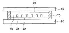
次に、図2に本発明の第1の製造方法における前記6)の工程を示す。図2中、30はクラッド用フィルム基材、32はコア、40はクラッド用硬化性樹脂の層をそれぞれ示す。また、60は表面に離型層(図示せず)を有する形状保持部材を、70はギャップ形成部材を、80は固定用治具をそれぞれ示す。ギャップ形成部材は、図示するように固定用治具と形状保持部材の間に置いても、クラッド用フィルム基材と形状保持部材の間に置いてもよい。
この状態でクラッド用硬化性樹脂を硬化させ、上部クラッド層を形成し、その後形状保持部材を上部クラッド層の表面から剥離する。Next, FIG. 2 shows the step 6) in the first production method of the present invention. In FIG. 2, 30 is a clad film substrate, 32 is a core, and 40 is a clad curable resin layer.
In this state, the clad curable resin is cured to form an upper clad layer, and then the shape maintaining member is peeled off from the surface of the upper clad layer.
また、図3に本発明の第2の製造方法における6)の工程を示す。図2と同じ符号で示すものは同じものを意味し、図2中50は上部フィルム基材を示す。
この状態でクラッド用硬化性樹脂を硬化させ、その後形状保持部材60をフィルム基材50から剥離する。FIG. 3 shows the step 6) in the second production method of the present invention. What is shown with the same code | symbol as FIG. 2 means the same thing, 50 in FIG. 2 shows an upper film base material.
In this state, the curable resin for cladding is cured, and then the
本発明の高分子光導波路の製造方法において、特に、鋳型形成用硬化性樹脂として硬化してゴム状になる液状シリコーンゴム、中でも液状ジメチルシロキサンゴムを用い、クラッド用フィルム基材として主鎖にノルボルネン構造を有しかつ側鎖にアルキルオキシカルボニル基等の極性基をもつ脂環式オレフィン樹脂を用いる組み合わせは、両者の密着性が特に高く、また、鋳型凹部構造の変形がなく、さらに凹部構造の断面積が極めて小さくても(たとえば10×10μmの矩形)毛細管現象により素早く凹部に硬化性樹脂を充填することができる。 In the method for producing a polymer optical waveguide of the present invention, in particular, a liquid silicone rubber that is cured as a curable resin for forming a mold and becomes a rubbery state, particularly a liquid dimethylsiloxane rubber, and a norbornene in the main chain as a film substrate for cladding. The combination using an alicyclic olefin resin having a structure and having a polar group such as an alkyloxycarbonyl group in the side chain has particularly high adhesion between the two, and there is no deformation of the mold recess structure, and the recess structure Even when the cross-sectional area is extremely small (for example, a rectangle of 10 × 10 μm), the concave portion can be quickly filled with the curable resin by the capillary phenomenon.
以下に実施例を示し本発明をさらに具体的に説明するが、本発明はこれらの実施例により限定されるものではない。
実施例1
Si基板に厚膜レジスト(マイクロケミカル(株)製、SU−8)をスピンコート法で塗布した後、80℃でプリベークし、フォトマスクを通して露光し、現像して、8本の、断面が正方形の凸部(幅:50μm、高さ:50μm、長さ:80mm)を形成した。凸部と凸部の間隔は250μmとした。次に、これを120℃でポストベークして、高分子光導波路作製用原盤を作製した。
次に、この原盤に離型剤を塗布した後、熱硬化性液状ジメチルシロキサンゴム(ダウ・コウニングアジア社製:SYLGARD184、粘度5000mPa.s)及びその硬化剤を混合したものを流し込み、120℃で30分間加熱して硬化させた後、剥離して、断面が矩形の前記凸部に対応する凹部を持った型(型の厚さ:5mm)を作製した。
さらに、平面形状が円形で鋳型厚さ方向の断面形状がテーパー状の貫通孔を、凹部の一端及び他端において、凹部と連通するように、打ち抜きにより形成して鋳型を作製した。鋳型のコア形成用硬化性樹脂が進入する側の貫通孔は、鋳型がクラッド用フィルム基材に接する面においては直径を4mm、鋳型の反対側の面においては直径を3.5mmとした。
鋳型は表面エネルギーが22dyn/cm、シェアゴム硬度が60、表面粗さが10nm以下、紫外線透過率80%以上であり、また、透明で下のものがよく観察できた。EXAMPLES Hereinafter, the present invention will be described more specifically with reference to examples. However, the present invention is not limited to these examples.
Example 1
After applying a thick film resist (SU-8, manufactured by Micro Chemical Co., Ltd.) to a Si substrate by a spin coating method, prebaking at 80 ° C., exposing through a photomask, development, and 8 cross sections are square. Convex portions (width: 50 μm, height: 50 μm, length: 80 mm) were formed. The interval between the protrusions was 250 μm. Next, this was post-baked at 120 ° C. to prepare a master for preparing a polymer optical waveguide.
Next, after applying a release agent to this master, a thermosetting liquid dimethylsiloxane rubber (manufactured by Dow Corning Asia Co., Ltd .: SYLGARD 184, viscosity 5000 mPa.s) and a mixture of the curing agent are poured, and 120 ° C. After being cured by heating for 30 minutes, it was peeled off to produce a mold having a concave portion corresponding to the convex portion having a rectangular cross section (mold thickness: 5 mm).
Further, a through hole having a circular planar shape and a tapered cross-sectional shape in the mold thickness direction was formed by punching so as to communicate with the recess at one end and the other end of the recess, thereby producing a mold. The through hole on the side where the curable resin for forming the core of the mold enters is 4 mm in diameter on the surface where the mold is in contact with the clad film substrate, and 3.5 mm in the surface on the opposite side of the mold.
The mold had a surface energy of 22 dyn / cm, a shear rubber hardness of 60, a surface roughness of 10 nm or less, an ultraviolet transmittance of 80% or more, and was transparent and well observed.
ガラス製の固定用治具の上に、鋳型より一回り大きい膜厚188μmのクラッド用フィルム基材(アートンフイルム、JSR(株)製、屈折率1.51)を置き、この上に前記鋳型を密着させた。次に、鋳型の進入側貫通孔に、粘度が600mPa・sの紫外線硬化性樹脂を数滴落とし、排出側(減圧吸引側)貫通孔から減圧吸引したところ、10分で前記凹部に紫外線硬化性樹脂が充填された。次いで、50mW/cm2のUV光を鋳型の上部から10分間照射して紫外線硬化させた。鋳型をアートンフイルムから剥離したところ、アートンフイルム上に前記原盤凸部と同じ形状のコアが形成された。コアの屈折率は1.55であった。(以下の工程はすべて固定用治具の上で行った。)A clad film base material (Arton Film, manufactured by JSR Corporation, refractive index 1.51) having a film thickness of 188 μm, which is slightly larger than the mold, is placed on a glass fixing jig, and the mold is placed thereon. Adhered. Next, a few drops of UV curable resin with a viscosity of 600 mPa · s were dropped into the entrance side through-hole of the mold, and vacuum suctioned from the discharge side (vacuum suction side) through-hole. Filled with resin. Next, 50 mW / cm2 of UV light was irradiated from the upper part of the mold for 10 minutes to be cured by ultraviolet rays. When the mold was peeled off from the arton film, a core having the same shape as the convex part of the master was formed on the arton film. The refractive index of the core was 1.55. (The following steps were all performed on a fixing jig.)
次に、コアを形成したアートンフイルム上に、硬化後の屈折率がアートンフイルムと同じ1.51である紫外線硬化性樹脂をディスペンサーで塗布した。(塗布厚は、以下のようにガラス板をスぺーサーの上に置いた場合、紫外線硬化性樹脂の塗布層表面とガラス板の間に間隙が生じないような厚さとした。)
図2に示すように、固定用治具の表面に厚さ260μmの金属製スぺーサー(ギャップ形成部材)を置き、スぺーサーの上に、サイトップ(旭硝子(株)製フッ素樹脂)を0.2μm被覆したガラス板(形状保持部材)を載せた。ガラス板を通して50mW/cm2のUV光を10分間照射して硬化させた。その後、サイトップ付きのガラス板を離型すると、全体の厚さが260μmのフレキシブルなフィルム状の高分子光導波路が得られた。
次に、Si用のブレードを備えたダイシングソーを使って、この高分子光導波路フィルムを、コアの長手方向に対し直角に切断し、鏡面を持ったコアを露出させ、光の入出力部とした。
得られた高分子導波路の伝搬損失は0.2dB/cmであった。Next, an ultraviolet curable resin having a refractive index after curing of 1.51 which is the same as that of the ARTON film was applied onto the ARTON film on which the core was formed, using a dispenser. (The coating thickness was such that when a glass plate was placed on a spacer as described below, no gap was formed between the surface of the UV curable resin coating layer and the glass plate.)
As shown in FIG. 2, a metal spacer (gap forming member) having a thickness of 260 μm is placed on the surface of the fixing jig, and Cytop (Fluorine resin manufactured by Asahi Glass Co., Ltd.) is placed on the spacer. A glass plate (shape holding member) coated with 0.2 μm was placed. Curing was performed by irradiating 50 mW / cm2 of UV light through a glass plate for 10 minutes. Thereafter, when the glass plate with cytop was released, a flexible film-like polymer optical waveguide having a total thickness of 260 μm was obtained.
Next, using a dicing saw equipped with a blade for Si, this polymer optical waveguide film is cut at a right angle to the longitudinal direction of the core, exposing the core having a mirror surface, did.
The propagation loss of the obtained polymer waveguide was 0.2 dB / cm.
実施例2
実施例1において用いたクラッド用フィルム基材(アートンフイルム)を、厚さ100μmのアートンフイルムに変更し、かつ、厚さが180μmの金属製スペーサーを用いる他は同様にして、全体の厚さが180μmのフィルム状の高分子光導波路を作製した。
得られた高分子導波路の伝搬損失は0.2dB/cmであった。Example 2
The overall thickness of the clad film base material (Arton film) used in Example 1 was changed to an Arton film having a thickness of 100 μm and a metal spacer having a thickness of 180 μm was used. A 180 μm film-shaped polymer optical waveguide was produced.
The propagation loss of the obtained polymer waveguide was 0.2 dB / cm.
実施例3
実施例1において、クラッド用フィルム基材として厚さ100μmのアートンフィルムを用いる他は、実施例1と同様にしてアートンフィルム上にコアを形成した。
次に、コアを形成したアートンフイルム上に、硬化後の屈折率がアートンフイルムと同じ1.51であるクラッド用紫外線硬化性樹脂をディスペンサーで塗布した。(塗布厚は、以下のように紫外線硬化性樹脂の表面にアートンフィルムを載せ、更にスぺーサーの上にガラス板を置いた場合、アートンフィルムとガラス板の間に間隙が生じないような厚さとした。)
図3に示すように、前記クラッド用紫外線硬化性樹脂の塗布面に膜厚100μmのアートンフィルムを載せた。次に、固定用治具の表面に厚さ300μmの金属製スぺーサー(ギャップ形成部材)を置き、スぺーサーの上に、サイトップ(旭硝子(株)製フッ素樹脂)を0.2μm被覆したガラス板(形状保持部材)を載せた。ガラス板を通して50mW/cm2のUV光を10分間照射して硬化させた。全体の厚さが300μmのフレキシブルなフィルム状の高分子光導波路が得られた。
次に、Si用のブレードを備えたダイシングソーを使って、この高分子光導波路フィルムを、コアの長手方向に対し直角に切断し、鏡面を持ったコアを露出させ、光の入出力部とした。
得られた高分子導波路の伝搬損失は0.1dB/cmであった。Example 3
In Example 1, a core was formed on the Arton film in the same manner as in Example 1 except that an Arton film having a thickness of 100 μm was used as the clad film substrate.
Next, a clad ultraviolet curable resin having a refractive index after curing of 1.51 which is the same as that of the ARTON film was applied onto the ARTON film on which the core was formed with a dispenser. (The coating thickness was such that when an Arton film was placed on the surface of the UV curable resin and a glass plate was placed on the spacer as described below, no gap was created between the Arton film and the glass plate. .)
As shown in FIG. 3, an Arton film having a thickness of 100 μm was placed on the coating surface of the ultraviolet curable resin for cladding. Next, a metal spacer (gap forming member) having a thickness of 300 μm is placed on the surface of the fixing jig, and Cytop (Fluorine resin manufactured by Asahi Glass Co., Ltd.) is coated on the spacer by 0.2 μm. The glass plate (shape holding member) was placed. Curing was performed by irradiating 50 mW / cm2 of UV light through a glass plate for 10 minutes. A flexible film-like polymer optical waveguide having a total thickness of 300 μm was obtained.
Next, using a dicing saw equipped with a blade for Si, this polymer optical waveguide film is cut at a right angle to the longitudinal direction of the core, exposing the core having a mirror surface, did.
The propagation loss of the obtained polymer waveguide was 0.1 dB / cm.
10 原型
12 光導波路コアに対応する凸部
20 鋳型
30 クラッド用フィルム基材
32 コア
40 クラッド用硬化性樹脂の層
50 上部フィルム基材
60 形状保持部材
70 ギャップ形成部材
80 固定用治具
100 高分子光導波路10
Claims (19)
Translated fromJapanesePriority Applications (1)
| Application Number | Priority Date | Filing Date | Title |
|---|---|---|---|
| JP2004009427AJP4273975B2 (en) | 2004-01-16 | 2004-01-16 | Method for producing flexible polymer optical waveguide |
Applications Claiming Priority (1)
| Application Number | Priority Date | Filing Date | Title |
|---|---|---|---|
| JP2004009427AJP4273975B2 (en) | 2004-01-16 | 2004-01-16 | Method for producing flexible polymer optical waveguide |
Publications (2)
| Publication Number | Publication Date |
|---|---|
| JP2005202230A JP2005202230A (en) | 2005-07-28 |
| JP4273975B2true JP4273975B2 (en) | 2009-06-03 |
Family
ID=34822473
Family Applications (1)
| Application Number | Title | Priority Date | Filing Date |
|---|---|---|---|
| JP2004009427AExpired - Fee RelatedJP4273975B2 (en) | 2004-01-16 | 2004-01-16 | Method for producing flexible polymer optical waveguide |
Country Status (1)
| Country | Link |
|---|---|
| JP (1) | JP4273975B2 (en) |
Families Citing this family (2)
| Publication number | Priority date | Publication date | Assignee | Title |
|---|---|---|---|---|
| KR101270996B1 (en)* | 2011-12-12 | 2013-06-04 | 광주과학기술원 | A casting mold for optical fiber and method for producing optical fiber using it |
| CN115876349A (en)* | 2022-12-02 | 2023-03-31 | 深圳技术大学 | Optical fiber temperature sensor manufacturing method, temperature sensor and temperature detection system |
- 2004
- 2004-01-16JPJP2004009427Apatent/JP4273975B2/ennot_activeExpired - Fee Related
Also Published As
| Publication number | Publication date |
|---|---|
| JP2005202230A (en) | 2005-07-28 |
Similar Documents
| Publication | Publication Date | Title |
|---|---|---|
| JP3945322B2 (en) | Optical element and manufacturing method thereof | |
| JP4196839B2 (en) | Method for producing polymer optical waveguide | |
| JP2008020722A (en) | Optical waveguide and manufacturing method thereof | |
| JP4144468B2 (en) | Multilayer polymer optical waveguide and method for manufacturing the same | |
| JP2004086144A (en) | Method for manufacturing macromolecular optical waveguide | |
| JP2006126568A (en) | Method for manufacturing polymer optical waveguide device | |
| JP2005181662A (en) | Method for manufacturing macromolecular optical waveguide | |
| JP2004144987A (en) | Manufacturing method of polymeric optical waveguide | |
| JP4265293B2 (en) | Method of manufacturing polymer optical waveguide integrated with mold and connector | |
| JP4581328B2 (en) | Polymer optical waveguide and optical element manufacturing method | |
| JP4175183B2 (en) | Method for producing polymer optical waveguide | |
| JP2009075288A (en) | Method of manufacturing polymer optical circuit | |
| JP2004069955A (en) | Method for manufacturing macromolecular optical waveguide | |
| JP2007233303A (en) | Method of manufacturing polymer optical waveguide module | |
| JP4534415B2 (en) | Method for producing polymer optical waveguide | |
| JP4292892B2 (en) | Method for producing laminated polymer optical waveguide and laminated polymer optical waveguide produced by this method | |
| JP4225207B2 (en) | Method for producing polymer optical waveguide | |
| JP4140475B2 (en) | Master for producing polymer optical waveguide and method for producing polymer optical waveguide | |
| JP4273975B2 (en) | Method for producing flexible polymer optical waveguide | |
| JP2005043652A (en) | Method for manufacturing polymer optical waveguide and apparatus for manufacturing the same | |
| JP4337559B2 (en) | Mold for producing polymer optical waveguide and method for producing polymer optical waveguide | |
| JP4517704B2 (en) | Method for producing polymer optical waveguide | |
| JP4259222B2 (en) | Cross-connect optical wiring sheet and manufacturing method thereof | |
| JP2007086330A (en) | Method for manufacturing polymer optical waveguide device | |
| JP4281548B2 (en) | Method for producing flexible polymer optical waveguide |
Legal Events
| Date | Code | Title | Description |
|---|---|---|---|
| A621 | Written request for application examination | Free format text:JAPANESE INTERMEDIATE CODE: A621 Effective date:20061219 | |
| A977 | Report on retrieval | Free format text:JAPANESE INTERMEDIATE CODE: A971007 Effective date:20080929 | |
| A131 | Notification of reasons for refusal | Free format text:JAPANESE INTERMEDIATE CODE: A131 Effective date:20081028 | |
| A521 | Written amendment | Free format text:JAPANESE INTERMEDIATE CODE: A523 Effective date:20081226 | |
| TRDD | Decision of grant or rejection written | ||
| A01 | Written decision to grant a patent or to grant a registration (utility model) | Free format text:JAPANESE INTERMEDIATE CODE: A01 Effective date:20090210 | |
| A01 | Written decision to grant a patent or to grant a registration (utility model) | Free format text:JAPANESE INTERMEDIATE CODE: A01 | |
| A61 | First payment of annual fees (during grant procedure) | Free format text:JAPANESE INTERMEDIATE CODE: A61 Effective date:20090223 | |
| R150 | Certificate of patent or registration of utility model | Free format text:JAPANESE INTERMEDIATE CODE: R150 | |
| FPAY | Renewal fee payment (event date is renewal date of database) | Free format text:PAYMENT UNTIL: 20120313 Year of fee payment:3 | |
| FPAY | Renewal fee payment (event date is renewal date of database) | Free format text:PAYMENT UNTIL: 20130313 Year of fee payment:4 | |
| FPAY | Renewal fee payment (event date is renewal date of database) | Free format text:PAYMENT UNTIL: 20130313 Year of fee payment:4 | |
| FPAY | Renewal fee payment (event date is renewal date of database) | Free format text:PAYMENT UNTIL: 20140313 Year of fee payment:5 | |
| LAPS | Cancellation because of no payment of annual fees |