JP4267659B2 - Manufacturing method of fin-type field effect transistor - Google Patents
Manufacturing method of fin-type field effect transistorDownload PDFInfo
- Publication number
- JP4267659B2 JP4267659B2JP2006327924AJP2006327924AJP4267659B2JP 4267659 B2JP4267659 B2JP 4267659B2JP 2006327924 AJP2006327924 AJP 2006327924AJP 2006327924 AJP2006327924 AJP 2006327924AJP 4267659 B2JP4267659 B2JP 4267659B2
- Authority
- JP
- Japan
- Prior art keywords
- fin
- field effect
- effect transistor
- type field
- manufacturing
- Prior art date
- Legal status (The legal status is an assumption and is not a legal conclusion. Google has not performed a legal analysis and makes no representation as to the accuracy of the status listed.)
- Expired - Fee Related
Links
Images

Classifications
- H—ELECTRICITY
- H01—ELECTRIC ELEMENTS
- H01L—SEMICONDUCTOR DEVICES NOT COVERED BY CLASS H10
- H01L21/00—Processes or apparatus adapted for the manufacture or treatment of semiconductor or solid state devices or of parts thereof
- H01L21/02—Manufacture or treatment of semiconductor devices or of parts thereof
- H01L21/04—Manufacture or treatment of semiconductor devices or of parts thereof the devices having potential barriers, e.g. a PN junction, depletion layer or carrier concentration layer
- H01L21/18—Manufacture or treatment of semiconductor devices or of parts thereof the devices having potential barriers, e.g. a PN junction, depletion layer or carrier concentration layer the devices having semiconductor bodies comprising elements of Group IV of the Periodic Table or AIIIBV compounds with or without impurities, e.g. doping materials
- H01L21/30—Treatment of semiconductor bodies using processes or apparatus not provided for in groups H01L21/20 - H01L21/26
- H01L21/31—Treatment of semiconductor bodies using processes or apparatus not provided for in groups H01L21/20 - H01L21/26 to form insulating layers thereon, e.g. for masking or by using photolithographic techniques; After treatment of these layers; Selection of materials for these layers
- H01L21/3105—After-treatment
- H—ELECTRICITY
- H01—ELECTRIC ELEMENTS
- H01L—SEMICONDUCTOR DEVICES NOT COVERED BY CLASS H10
- H01L21/00—Processes or apparatus adapted for the manufacture or treatment of semiconductor or solid state devices or of parts thereof
- H01L21/02—Manufacture or treatment of semiconductor devices or of parts thereof
- H01L21/02041—Cleaning
- H01L21/02057—Cleaning during device manufacture
- H—ELECTRICITY
- H10—SEMICONDUCTOR DEVICES; ELECTRIC SOLID-STATE DEVICES NOT OTHERWISE PROVIDED FOR
- H10D—INORGANIC ELECTRIC SEMICONDUCTOR DEVICES
- H10D30/00—Field-effect transistors [FET]
- H10D30/01—Manufacture or treatment
- H10D30/021—Manufacture or treatment of FETs having insulated gates [IGFET]
- H10D30/024—Manufacture or treatment of FETs having insulated gates [IGFET] of fin field-effect transistors [FinFET]
- H10D30/0245—Manufacture or treatment of FETs having insulated gates [IGFET] of fin field-effect transistors [FinFET] by further thinning the channel after patterning the channel, e.g. using sacrificial oxidation on fins
Landscapes
- Engineering & Computer Science (AREA)
- Physics & Mathematics (AREA)
- Condensed Matter Physics & Semiconductors (AREA)
- General Physics & Mathematics (AREA)
- Manufacturing & Machinery (AREA)
- Computer Hardware Design (AREA)
- Microelectronics & Electronic Packaging (AREA)
- Power Engineering (AREA)
- Thin Film Transistor (AREA)
Description
Translated fromJapanese本発明はSOIウエハを用いてフィン型の電界効果トランジスタを製造する方法に関する。 The present invention relates to a method of manufacturing a fin-type field effect transistor using an SOI wafer.
近時、集積回路の集積度が益々高まっており、集積回路に用いられるCMOS等の電界効果トランジスタ(FET)の微細化が求められている。このため、チャネル長の短縮化、ゲート絶縁膜の厚さの低減、不純物ドーピング濃度の上昇等が試みられている。しかしながら、チャネル長の短縮化はほぼ限界が来ており、現在の構造を維持したままより微細化を進めることが困難となりつつある。 Recently, the degree of integration of integrated circuits is increasing, and there is a demand for miniaturization of field effect transistors (FETs) such as CMOS used in integrated circuits. For this reason, attempts have been made to shorten the channel length, reduce the thickness of the gate insulating film, increase the impurity doping concentration, and the like. However, the shortening of the channel length has almost reached its limit, and it is becoming difficult to further miniaturize while maintaining the current structure.
このような問題を解決してさらなる電界効果トランジスタの微細化、高集積化を図ることができる技術として、Siウエハにフィン状の突起を形成してチャネル面を垂直にした3次元型の電界効果トランジスタ、いわゆるフィン型電界効果トランジスタが知られている(例えば特許文献1)。 As a technique for solving such problems and further miniaturizing and increasing the integration of field effect transistors, a three-dimensional field effect in which fin-like projections are formed on a Si wafer and the channel surface is vertical is used. A transistor, a so-called fin-type field effect transistor is known (for example, Patent Document 1).
一方、このように集積回路の高集積化にともなって電界効果トランジスタのオフ状態の漏電流が問題となるため、このような漏電流を低減することができるSOI(Silicon On Insulator)ウエハが用いられつつある。SOIウエハは、単結晶シリコン基板ウエハに、シリコン酸化物からなる埋め込み酸化物(Buried Oxide)層を形成し、その上に単結晶シリコン層を成長させたものである。このようなSOIウエハに上記フィン型電界効果トランジスタを形成する技術が特許文献2に開示されている。 On the other hand, since the leakage current in the off state of the field effect transistor becomes a problem as the integrated circuit becomes highly integrated, an SOI (Silicon On Insulator) wafer that can reduce such a leakage current is used. It's getting on. The SOI wafer is obtained by forming a buried oxide layer made of silicon oxide on a single crystal silicon substrate wafer and growing a single crystal silicon layer on the buried oxide layer. A technique for forming the fin-type field effect transistor on such an SOI wafer is disclosed in
フィン型電界効果トランジスタを製造する際において、フィンの形成には、以下の方法が一般に用いられる。
まず、ウエハにプラズマエッチングを施してフィン状の突起部を形成する。この突起部は最終的に形成されるフィンよりも大きなサイズとする。しかして、この突起部の表面にはプラズマによるダメージが生じているので、次工程として、ダメージを含む表面を酸化して犠牲酸化膜を形成し、これを希フッ酸によるウエットエッチングで除去することにより、清浄な表面を有し、最初に形成した突起部よりも小さいサイズ(最終的に形成されるものとほぼ同一サイズ)のフィンを形成する。When manufacturing a fin-type field effect transistor, the following method is generally used for forming the fin.
First, the wafer is subjected to plasma etching to form fin-like protrusions. The protrusion is larger in size than the finally formed fin. Since the surface of this protrusion is damaged by plasma, the next step is to oxidize the damaged surface to form a sacrificial oxide film, which is removed by wet etching with dilute hydrofluoric acid. Thus, a fin having a clean surface and a size smaller than the projection formed first (substantially the same size as that finally formed) is formed.
このように、プラズマエッチングによるダメージを犠牲酸化膜のウエットエッチングにより除去する方法は、その操作が簡単であり、また、プラズマエッチングのみでは形成できないサイズ(例えば幅が30〜40nm)のフィンを形成することができる。 As described above, the method of removing damage caused by plasma etching by wet etching of the sacrificial oxide film is simple in operation, and fins having a size (for example, a width of 30 to 40 nm) that cannot be formed only by plasma etching are formed. be able to.
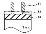
しかしながら、ウエハとして上記のSOIウエハを用いた場合、すなわち、埋め込み酸化物層上の単結晶シリコン層にプラズマエッチングを施してフィン状の突起部を形成し、この突起部に生じたダメージを、犠牲酸化膜のウエットエッチングにより除去する場合には、図2に示すように、形成されるフィン51の基端部分にくびれ(オーバーハング)52が生じてしまう。 However, when the above-described SOI wafer is used as a wafer, that is, the single crystal silicon layer on the buried oxide layer is subjected to plasma etching to form a fin-like protrusion, and the damage caused to the protrusion is sacrificed. When the oxide film is removed by wet etching, as shown in FIG. 2, a constriction (overhang) 52 occurs at the base end portion of the
このくびれ52は次のようにして形成される。すなわち、プラズマエッチングによって露出した埋め込み酸化物層53の上部が、犠牲酸化膜とともに希フッ酸によってウエットエッチングされ(ウエットエッチングされる前の埋め込み酸化物層を点線で示す)、さらに、ウエットエッチングの等方性のためにフィン51の直下(露出していない)のシリコン酸化物まで部分的にエッチング(サイドエッチング)されてしまうことにより形成されるものである。 The
そして、このようなくびれが生じると、その部分にゲート配線材料等の残渣が生じ、これがデバイス性能に悪影響を及ぼすおそれがある。従来は、このような残渣を薬液洗浄等で除去することが試みられてきたが、洗浄工程は煩雑であり、また、これらの残渣を洗浄工程によって完全に除去することは困難である。さらに、このようなくびれが生じると、フィンの倒れ等の強度的な問題も懸念される。
本発明はかかる事情に鑑みてなされたものであって、SOIウエハを用いて、プラズマエッチングにより生じたダメージを犠牲酸化膜のウエットエッチングにより除去する工程を含むものでありながら、フィンの基端部分にくびれのないフィン型電界効果トランジスタを簡単かつ確実に製造することができる方法を提供することを目的とする。 The present invention has been made in view of such circumstances, and includes a step of removing damage caused by plasma etching by wet etching of a sacrificial oxide film using an SOI wafer. An object of the present invention is to provide a method capable of easily and reliably manufacturing a fin-type field effect transistor without constriction.
上記課題を解決するため、本発明では、Si基板上にSiO2系材料からなる埋め込み酸化物層が形成され、さらにその上に単結晶シリコン層が形成されてなるSOIウエハを用いてフィン型電界効果トランジスタを製造する方法であって、前記単結晶シリコン層を下地の埋め込み酸化物層が露出するまで選択的にプラズマエッチングしてフィン状の突起部を形成する工程と、前記突起部に生じたダメージを含む表面を酸化して犠牲酸化膜を形成する工程と、この犠牲酸化膜をウエットエッチングにより除去して、清浄な表面を有するフィンを形成する工程と、前記埋め込み酸化物層を加熱してリフローさせる工程とを含むことを特徴とするフィン型電界効果トランジスタの製造方法を提供する。In order to solve the above problems, in the present invention, a fin-type electric field is formed using an SOI wafer in which a buried oxide layer made of a SiO2 material is formed on a Si substrate and a single crystal silicon layer is further formed thereon. A method of manufacturing an effect transistor, the step of selectively plasma-etching the single crystal silicon layer until the underlying buried oxide layer is exposed to form a fin-like protrusion, and the protrusion formed on the protrusion A step of oxidizing a surface including damage to form a sacrificial oxide film; a step of removing the sacrificial oxide film by wet etching to form a fin having a clean surface; and heating the buried oxide layer. And a reflow process. A method for manufacturing a fin-type field effect transistor is provided.
本発明において、埋め込み酸化物層は、リンやボロン等の不純物が添加されて低融点化されたSiO2系材料からなるものを好適に用いることができ、特に、不純物としてリンおよびボロンを含有するBPSGを用いることが好ましい。In the present invention, the buried oxide layer can be suitably made of a SiO2 material having a low melting point added with impurities such as phosphorus and boron, and particularly contains phosphorus and boron as impurities. It is preferable to use BPSG.
上記リフロー工程において、埋め込み酸化物層がBPSGからなる場合には、900℃以下、例えば800℃±100℃の温度に加熱してBPSGをリフローさせることができる。 In the reflow step, when the buried oxide layer is made of BPSG, the BPSG can be reflowed by heating to a temperature of 900 ° C. or lower, for example, 800 ° C. ± 100 ° C.
本発明において、プラズマエッチング工程により形成される突起部の幅(w0)が60〜80nmであり、最終的に形成されるフィンの幅(w)が30〜40nmであってよく、その際の比率(w0/w)は、1.5〜2.0とすることができる。また、前記犠牲酸化膜を除去する際に、エッチング液として希フッ酸を使用することができる。In the present invention, the width (w0 ) of the protrusion formed by the plasma etching process may be 60 to 80 nm, and the width (w) of the fin finally formed may be 30 to 40 nm. The ratio (w0 / w) can be 1.5 to 2.0. In removing the sacrificial oxide film, dilute hydrofluoric acid can be used as an etchant.
本発明の製造方法によれば、埋め込み酸化物層を加熱してリフローさせるという工程を付加することにより、SOIウエハを用いて、プラズマエッチングにより生じたダメージを犠牲酸化膜のウエットエッチングにより除去する工程を含むものでありながら、フィンの基端部分にくびれのないフィン型電界効果トランジスタを簡単かつ確実に製造することができる。 According to the manufacturing method of the present invention, the step of removing the damage caused by the plasma etching by wet etching of the sacrificial oxide film using the SOI wafer by adding the step of heating and reflowing the buried oxide layer. However, it is possible to easily and surely manufacture a fin-type field effect transistor having no constriction at the base end portion of the fin.
以下、本発明の実施形態について説明する。
図1(a)〜(e)は、本発明の一実施形態に係るフィン型電界効果トランジスタの製造方法を示す工程断面図である。この製造方法は、SOIウエハを用いる製造方法であって、プラズマエッチングにより突起を形成する工程と、突起に犠牲酸化膜を形成する工程と、犠牲酸化膜をウエットエッチングにより除去する工程と、埋め込み酸化物層をリフローする工程とを含む。Hereinafter, embodiments of the present invention will be described.
1A to 1E are process cross-sectional views illustrating a method for manufacturing a fin-type field effect transistor according to an embodiment of the present invention. This manufacturing method is a manufacturing method using an SOI wafer, a step of forming a protrusion by plasma etching, a step of forming a sacrificial oxide film on the protrusion, a step of removing the sacrificial oxide film by wet etching, and a buried oxidation. Reflowing the material layer.
本実施形態においては、まず、図1(a)に示すような層構成のSOIウエハを準備する。このSOIウエハは、単結晶シリコンからなるシリコン基板1と、SiO2系材料からなる埋め込み酸化物層2と、単結晶シリコン層3とが積層されてなる。In this embodiment, first, an SOI wafer having a layer structure as shown in FIG. This SOI wafer is formed by laminating a
埋め込み酸化物層2は、リンやボロン等の1または2以上の不純物を添加したSiO2系材料を用いることが好ましい。リンやボロン等の不純物を含有させることにより、埋め込み酸化物層2の酸化物の融点を下げることができ、延いてはリフロー工程における加熱温度を低下させることができる。かかる観点から埋め込み酸化物層2を構成するSiO2系材料としてはボロンおよびリンを含有したBPSG(BoroPhosphoSilicate Glass)を好適に用いることができる。The buried
埋め込み酸化物層2の膜厚は、例えば130〜160nmとされる。この範囲であれば、電界効果トランジスタのオフ状態の漏電流を十分に抑制することができる。
埋め込み酸化物層2上の単結晶シリコン層3の膜厚は、最終的に形成されるフィンの高さを規定するものであり、例えば50〜100nmとされる。The thickness of the buried
The film thickness of the single crystal silicon layer 3 on the buried
プラズマエッチング工程では、単結晶シリコン層3の上にハードマスク4のパターンを形成した後プラズマエッチングを行う。これにより、単結晶シリコン層3が選択的に削られて埋め込み酸化物層2の一部が露出し、図1(b)に示すようなフィン状の突起部5が形成される。 In the plasma etching step, the pattern of the hard mask 4 is formed on the single crystal silicon layer 3 and then plasma etching is performed. As a result, the single crystal silicon layer 3 is selectively scraped to expose a part of the buried
プラズマエッチングとしては特に限定されるものではなく、従来公知の装置を使用し、常法に従って行うことができる。
プラズマエッチングの際にダメージ層が形成されることから、突起部5の幅を最終的に形成されるフィンの幅よりも大きく設定して、ダメージ層を除去する際の削り代を確保するようにする。The plasma etching is not particularly limited, and can be performed according to a conventional method using a conventionally known apparatus.
Since a damage layer is formed during plasma etching, the width of the
例えば、幅(w)が30〜40nmのフィンを形成する場合において、プラズマエッチング工程によって形成される突起部の幅(w0)は60〜80nmであることが好ましい。この場合に、フィンの幅(w)に対する突起部の幅(w0)の比率(w0/w)は1.5〜2.0であることが好ましい。For example, when a fin having a width (w) of 30 to 40 nm is formed, the width (w0 ) of the protrusion formed by the plasma etching process is preferably 60 to 80 nm. In this case, the ratio (w0 / w) of the width (w0 ) of the protrusion to the width (w) of the fin is preferably 1.5 to 2.0.
比率(w0/w)が1.5未満である場合には、後述する犠牲酸化膜を形成してウエットエッチングすることによるダメージ層除去の際の削り代を十分に確保することができない。一方、(w0/w)が2.0を超える場合には、削り代が過大となって、犠牲酸化膜の除去に長い時間を要したり、埋め込み酸化物層のエッチングが必要以上に進行したりする虞がある。When the ratio (w0 / w) is less than 1.5, it is not possible to secure a sufficient machining allowance when removing a damaged layer by forming a sacrificial oxide film described later and performing wet etching. On the other hand, when (w0 / w) exceeds 2.0, the cutting allowance becomes excessive, and it takes a long time to remove the sacrificial oxide film, or the embedded oxide layer is etched more than necessary. There is a risk of doing.
プラズマエッチング工程終了後、ハードマスク4を除去して犠牲酸化工程を実施する。犠牲酸化工程では、ダメージを含む突起部5の表面を酸化することにより、図1(c)に示すような犠牲酸化膜6を形成する。犠牲酸化膜6の形成方法としては特に限定されるものではなく、従来公知の装置を用いて公知の方法で形成することができる。例えば、酸化性ガスの存在下で加熱する熱酸化の手法で形成することができる。 After the plasma etching process, the hard mask 4 is removed and a sacrificial oxidation process is performed. In the sacrificial oxidation step, the sacrificial oxide film 6 as shown in FIG. 1C is formed by oxidizing the surface of the
次のウエットエッチング工程により清浄な表面のフィンを形成するために、犠牲酸化膜6は、突起部5のダメージが存在する領域(ダメージ層)を包含できる膜厚を有していることが必要である。犠牲酸化膜6の膜厚は、例えば30〜40nmとされ、この膜厚は酸化処理条件を制御することにより適宜調整することができる。 In order to form a fin with a clean surface by the next wet etching process, the sacrificial oxide film 6 needs to have a film thickness that can include a region (damage layer) where the damage of the
ウエットエッチング工程では、図1(d)に示すように、犠牲酸化膜6をウエットエッチングで除去する。使用するエッチング液としては、シリコン酸化物はエッチング可能であるが、単結晶シリコンをエッチングしない(フィンとなる下地に新たなダメージを与えない)薬液の中から選択される。具体的には、従来この分野で多用されているフッ酸(HF)の水溶液を使用することが好ましく、希フッ酸(HF濃度=1〜5質量%)を使用することが特に好ましい。 In the wet etching process, as shown in FIG. 1D, the sacrificial oxide film 6 is removed by wet etching. As an etchant to be used, silicon oxide can be etched, but is selected from chemicals that do not etch single crystal silicon (does not cause new damage to the base to be a fin). Specifically, it is preferable to use an aqueous solution of hydrofluoric acid (HF) that has been frequently used in this field, and it is particularly preferable to use dilute hydrofluoric acid (HF concentration = 1 to 5 mass%).
犠牲酸化膜6を除去することにより、プラズマエッチングによって突起部5の表面に生じたダメージが除去され、清浄な表面を有するフィン7が埋め込み酸化物層2上に形成される。このように形成されたフィン7の幅(w)は、例えば30〜40nmとされる。 By removing the sacrificial oxide film 6, damage caused on the surface of the
ところで、上述したように、犠牲酸化膜6を形成した後のウエットエッチングでは、犠牲酸化膜6とともに埋め込み酸化物層もエッチングされ、この際のエッチングは等方的であることから、埋め込み酸化物層の露出部分のみならず非露出部分もエッチング(サイドエッチング)されることから、形成されたフィン7の基端部分にはくびれ8が不可避的に生じる。 By the way, as described above, in the wet etching after the sacrificial oxide film 6 is formed, the buried oxide layer is also etched together with the sacrificial oxide film 6, and the etching at this time is isotropic. Since not only the exposed portion but also the unexposed portion is etched (side-etched), a
そこで、本実施形態では、ウエットエッチング工程の後、リフロー工程を実施して、埋め込み酸化物層2を加熱してリフローさせ、このようなくびれを解消させる。リフロー工程では、埋め込み酸化物層2をリフローさせる必要があることから、その加熱温度は、埋め込み酸化物層2を構成するSiO2系材料の融点以上とされる。例えば、埋め込み酸化物層2が不純物を添加しないSiO2からなる場合には1000〜2000℃とされる。Therefore, in the present embodiment, after the wet etching process, a reflow process is performed to heat and reflow the buried
しかし、このような高温では工程上、種々の不都合が生じるおそれがあるため、上述したように埋め込み酸化物層2としてリンやボロン等の1または2以上の不純物を添加して低融点化されたSiO2系材料を用いて、リフロー工程での加熱温度を低下させることが好ましい。特に、SiO2系材料としてBPSGを用いた場合には、加熱温度を900℃以下といった低温でも埋め込み酸化物層2を確実にリフローさせることができる。より好ましい加熱温度は、800℃前後(800℃±100℃)である。However, since various inconveniences may occur in the process at such a high temperature, the melting point is lowered by adding one or more impurities such as phosphorus and boron as the buried
リフロー工程での加熱処理は、通常、窒素ガスなどの不活性ガスの雰囲気下で行う。処理時の圧力としては特に限定されるものではなく、例えば100〜500Torr(13330〜66650Pa)で行うことができる。また、処理時間としては30〜300sec程度である。 The heat treatment in the reflow process is usually performed in an atmosphere of an inert gas such as nitrogen gas. It does not specifically limit as a pressure at the time of a process, For example, it can carry out by 100-500Torr (13330-66650Pa). The processing time is about 30 to 300 seconds.
このように埋め込み酸化物層2をリフローさせることにより、埋め込み酸化物層2が流動して、フィンの基端部分のくびれにリフローした状態のシリコン酸化物が流入した状態、あるいは、リフローした状態の埋め込み酸化物層2中にフィンの基端部が沈み込んだ状態となって、図1(e)に示すようにくびれが確実に消滅した状態となり、その後冷却することにより、埋め込み酸化物層2はくびれが消滅した状態のまま固化される。このため、フィン7は埋め込み酸化物層2によって確実に保持される。 By reflowing the buried
このようなリフロー工程によりくびれを解消した後、ゲート配線の形成や拡散領域の形成等の工程を常法に従って実施し、所望のフィン型電界効果トランジスタを得る。 After eliminating the constriction by such a reflow process, steps such as formation of a gate wiring and formation of a diffusion region are performed according to a conventional method to obtain a desired fin-type field effect transistor.
このように、本実施形態で製造されたフィン型電界効果トランジスタにはフィン7の基端部にくびれが存在しないので、くびれにゲート配線材料等が残留することに起因するデバイス性能への悪影響は発生しない。また、フィン7が埋め込み酸化物層2によって確実に保持されるので、フィンが倒れるという強度的な問題も生じさせない。 Thus, since the fin field effect transistor manufactured in this embodiment has no constriction at the base end portion of the
1;シリコン基板
2;埋め込み酸化物層
3;SOI層
4;ハードマスク
5;突起部
6;犠牲酸化膜
7;フィン
8;くびれDESCRIPTION OF
Claims (8)
Translated fromJapanese前記単結晶シリコン層を下地の埋め込み酸化物層が露出するまで選択的にプラズマエッチングしてフィン状の突起部を形成する工程と、
前記突起部に生じたダメージを含む表面を酸化して犠牲酸化膜を形成する工程と、
この犠牲酸化膜をウエットエッチングにより除去して、清浄な表面を有するフィンを形成する工程と、
前記埋め込み酸化物層を加熱してリフローさせるリフロー工程と
を含むことを特徴とするフィン型電界効果トランジスタの製造方法。A method of manufacturing a fin-type field effect transistor using an SOI wafer in which a buried oxide layer made of a SiO2 based material is formed on a Si substrate and a single crystal silicon layer is further formed thereon,
Selectively etching the single crystal silicon layer until the underlying buried oxide layer is exposed to form fin-like protrusions;
Forming a sacrificial oxide film by oxidizing a surface including damage generated in the protrusion; and
Removing the sacrificial oxide film by wet etching to form a fin having a clean surface;
And a reflow process of heating and reflowing the buried oxide layer.
Priority Applications (2)
| Application Number | Priority Date | Filing Date | Title |
|---|---|---|---|
| JP2006327924AJP4267659B2 (en) | 2006-12-05 | 2006-12-05 | Manufacturing method of fin-type field effect transistor |
| US11/999,224US20080132077A1 (en) | 2006-12-05 | 2007-12-03 | Method for manufacturing a fin field effect transistor |
Applications Claiming Priority (1)
| Application Number | Priority Date | Filing Date | Title |
|---|---|---|---|
| JP2006327924AJP4267659B2 (en) | 2006-12-05 | 2006-12-05 | Manufacturing method of fin-type field effect transistor |
Publications (2)
| Publication Number | Publication Date |
|---|---|
| JP2008141097A JP2008141097A (en) | 2008-06-19 |
| JP4267659B2true JP4267659B2 (en) | 2009-05-27 |
Family
ID=39476352
Family Applications (1)
| Application Number | Title | Priority Date | Filing Date |
|---|---|---|---|
| JP2006327924AExpired - Fee RelatedJP4267659B2 (en) | 2006-12-05 | 2006-12-05 | Manufacturing method of fin-type field effect transistor |
Country Status (2)
| Country | Link |
|---|---|
| US (1) | US20080132077A1 (en) |
| JP (1) | JP4267659B2 (en) |
Families Citing this family (6)
| Publication number | Priority date | Publication date | Assignee | Title |
|---|---|---|---|---|
| US8106459B2 (en) | 2008-05-06 | 2012-01-31 | Taiwan Semiconductor Manufacturing Company, Ltd. | FinFETs having dielectric punch-through stoppers |
| US8263462B2 (en)* | 2008-12-31 | 2012-09-11 | Taiwan Semiconductor Manufacturing Company, Ltd. | Dielectric punch-through stoppers for forming FinFETs having dual fin heights |
| TWI442014B (en) | 2010-11-24 | 2014-06-21 | Ind Tech Res Inst | Heat dissipating component and heat dissipating component processing method |
| US8993402B2 (en)* | 2012-08-16 | 2015-03-31 | International Business Machines Corporation | Method of manufacturing a body-contacted SOI FINFET |
| KR102150254B1 (en) | 2014-09-15 | 2020-09-02 | 삼성전자주식회사 | Manufacturing method of semiconductor device |
| US10164108B2 (en)* | 2014-10-17 | 2018-12-25 | Taiwan Semiconductor Manufacturing Co., Ltd. | Fin field effect transistor (FinFET) device and method for forming the same |
Family Cites Families (4)
| Publication number | Priority date | Publication date | Assignee | Title |
|---|---|---|---|---|
| US20020089032A1 (en)* | 1999-08-23 | 2002-07-11 | Feng-Yi Huang | Processing method for forming dislocation-free silicon-on-insulator substrate prepared by implantation of oxygen |
| DE10012112C2 (en)* | 2000-03-13 | 2002-01-10 | Infineon Technologies Ag | Bridge field effect transistor and method for producing a bridge field effect transistor |
| US6909151B2 (en)* | 2003-06-27 | 2005-06-21 | Intel Corporation | Nonplanar device with stress incorporation layer and method of fabrication |
| US6960509B1 (en)* | 2004-06-30 | 2005-11-01 | Freescale Semiconductor, Inc. | Method of fabricating three dimensional gate structure using oxygen diffusion |
- 2006
- 2006-12-05JPJP2006327924Apatent/JP4267659B2/ennot_activeExpired - Fee Related
- 2007
- 2007-12-03USUS11/999,224patent/US20080132077A1/ennot_activeAbandoned
Also Published As
| Publication number | Publication date |
|---|---|
| JP2008141097A (en) | 2008-06-19 |
| US20080132077A1 (en) | 2008-06-05 |
Similar Documents
| Publication | Publication Date | Title |
|---|---|---|
| KR101024813B1 (en) | Configuration for Etching Metal Hard Mask Material of Semiconductor Process | |
| US7696045B2 (en) | Method of manufacturing semiconductor device | |
| TWI356451B (en) | Wet etch suitable for creating square cuts in si a | |
| JP4267659B2 (en) | Manufacturing method of fin-type field effect transistor | |
| JPH0621018A (en) | Dry etching method | |
| JP2007081383A (en) | Microstructure manufacturing method | |
| CN104241136B (en) | The fin field-effect transistor spacer-etch improved for embedded SiGe | |
| TWI593105B (en) | Method for forming semiconductor device structure | |
| JP2001345375A (en) | Semiconductor device and method of manufacturing the same | |
| CN100452345C (en) | Method of manufacturing a semiconductor device, and a semiconductor substrate | |
| CN104992903A (en) | High-quality gate oxide forming method | |
| JP2008060383A (en) | Manufacturing method of semiconductor device | |
| JP2007110005A (en) | Manufacturing method of semiconductor device | |
| TWI322472B (en) | Method for fabricating semiconductor device with gate | |
| CN104701262B (en) | A kind of forming method of semiconductor devices | |
| JP3853096B2 (en) | Trench isolation method for semiconductor integrated circuit | |
| US8691705B2 (en) | Method of patterning metal alloy material layer having hafnium and molybdenum | |
| JP2006269551A (en) | Semiconductor device and its manufacturing method | |
| JP2007123548A (en) | Manufacturing method of semiconductor device | |
| JP3552913B2 (en) | Device isolation method for semiconductor device | |
| KR100875154B1 (en) | Semiconductor device formation method | |
| JP2006080321A (en) | Semiconductor device and manufacturing method thereof | |
| JP2010109163A (en) | Method of manufacturing semiconductor device, and composition for semiconductor cleaning | |
| KR20050075179A (en) | Method of forming a trench type gate in a semiconductor device | |
| JP2007501512A (en) | Manufacturing method of semiconductor device having bipolar transistor and device having bipolar transistor |
Legal Events
| Date | Code | Title | Description |
|---|---|---|---|
| A977 | Report on retrieval | Free format text:JAPANESE INTERMEDIATE CODE: A971007 Effective date:20090122 | |
| TRDD | Decision of grant or rejection written | ||
| A01 | Written decision to grant a patent or to grant a registration (utility model) | Free format text:JAPANESE INTERMEDIATE CODE: A01 Effective date:20090217 | |
| A01 | Written decision to grant a patent or to grant a registration (utility model) | Free format text:JAPANESE INTERMEDIATE CODE: A01 | |
| A61 | First payment of annual fees (during grant procedure) | Free format text:JAPANESE INTERMEDIATE CODE: A61 Effective date:20090218 | |
| R150 | Certificate of patent or registration of utility model | Free format text:JAPANESE INTERMEDIATE CODE: R150 | |
| FPAY | Renewal fee payment (event date is renewal date of database) | Free format text:PAYMENT UNTIL: 20120227 Year of fee payment:3 | |
| FPAY | Renewal fee payment (event date is renewal date of database) | Free format text:PAYMENT UNTIL: 20150227 Year of fee payment:6 | |
| R250 | Receipt of annual fees | Free format text:JAPANESE INTERMEDIATE CODE: R250 | |
| LAPS | Cancellation because of no payment of annual fees |