JP4260587B2 - Pattern defect inspection system - Google Patents
Pattern defect inspection systemDownload PDFInfo
- Publication number
- JP4260587B2 JP4260587B2JP2003325526AJP2003325526AJP4260587B2JP 4260587 B2JP4260587 B2JP 4260587B2JP 2003325526 AJP2003325526 AJP 2003325526AJP 2003325526 AJP2003325526 AJP 2003325526AJP 4260587 B2JP4260587 B2JP 4260587B2
- Authority
- JP
- Japan
- Prior art keywords
- image
- light
- illumination
- pattern
- defect inspection
- Prior art date
- Legal status (The legal status is an assumption and is not a legal conclusion. Google has not performed a legal analysis and makes no representation as to the accuracy of the status listed.)
- Expired - Fee Related
Links
Images


Classifications
- G—PHYSICS
- G01—MEASURING; TESTING
- G01N—INVESTIGATING OR ANALYSING MATERIALS BY DETERMINING THEIR CHEMICAL OR PHYSICAL PROPERTIES
- G01N21/00—Investigating or analysing materials by the use of optical means, i.e. using sub-millimetre waves, infrared, visible or ultraviolet light
- G01N21/84—Systems specially adapted for particular applications
- G01N21/88—Investigating the presence of flaws or contamination
- G01N21/95—Investigating the presence of flaws or contamination characterised by the material or shape of the object to be examined
- G01N21/9501—Semiconductor wafers
- G—PHYSICS
- G01—MEASURING; TESTING
- G01N—INVESTIGATING OR ANALYSING MATERIALS BY DETERMINING THEIR CHEMICAL OR PHYSICAL PROPERTIES
- G01N21/00—Investigating or analysing materials by the use of optical means, i.e. using sub-millimetre waves, infrared, visible or ultraviolet light
- G01N21/17—Systems in which incident light is modified in accordance with the properties of the material investigated
- G01N21/47—Scattering, i.e. diffuse reflection
- G01N21/4788—Diffraction
- G—PHYSICS
- G01—MEASURING; TESTING
- G01N—INVESTIGATING OR ANALYSING MATERIALS BY DETERMINING THEIR CHEMICAL OR PHYSICAL PROPERTIES
- G01N21/00—Investigating or analysing materials by the use of optical means, i.e. using sub-millimetre waves, infrared, visible or ultraviolet light
- G01N21/84—Systems specially adapted for particular applications
- G01N21/88—Investigating the presence of flaws or contamination
- G01N21/95—Investigating the presence of flaws or contamination characterised by the material or shape of the object to be examined
- G01N21/956—Inspecting patterns on the surface of objects
Landscapes
- Physics & Mathematics (AREA)
- Health & Medical Sciences (AREA)
- Life Sciences & Earth Sciences (AREA)
- Chemical & Material Sciences (AREA)
- Analytical Chemistry (AREA)
- Biochemistry (AREA)
- General Health & Medical Sciences (AREA)
- General Physics & Mathematics (AREA)
- Immunology (AREA)
- Pathology (AREA)
- Investigating Materials By The Use Of Optical Means Adapted For Particular Applications (AREA)
- Testing Or Measuring Of Semiconductors Or The Like (AREA)
- Length Measuring Devices By Optical Means (AREA)
- Image Processing (AREA)
- Image Analysis (AREA)
Description
Translated fromJapanese本発明は、被検査パターンの欠陥(ショートや断線など)や異物を検出するパターン検査、異物検査に係り、特に半導体ウェハや液晶ディスプレイ、ホトマスクなどの被検査パターンにおける欠陥・異物を検査する被検査パターンの欠陥検査装置及び方法に適用して有効な技術に関するものである。なお、以下において、欠陥は異物を含むものとする。 The present invention relates to a pattern inspection for detecting defects (short circuit, disconnection, etc.) and foreign matter in a pattern to be inspected, and a foreign matter inspection. The present invention relates to a technique effective when applied to a pattern defect inspection apparatus and method. In the following, it is assumed that the defect includes a foreign substance.
本発明者が検討したところによれば、被検査パターンの欠陥を検出するパターン検査技術に関しては、以下のような技術が考えられる。 According to a study by the present inventors, the following techniques can be considered as a pattern inspection technique for detecting a defect of a pattern to be inspected.
たとえば、従来、この種の検査装置は、特許文献1に記載のように、被検査パターンを移動させつつ、イメージセンサ等の撮像素子により被検査パターンの画像を検出し、検出した画像信号と定めた時間遅らせた画像信号の濃淡を比較することにより、不一致を欠陥として認識するものであった。 For example, conventionally, as described in
また、被検査パターンの欠陥検査に関する従来技術としては、特許文献2が知られている。この特許文献2には、メモリマット部などのパターン密度が高い領域と周辺回路などのパターン密度が低い領域とがチップ内に混在する半導体ウェハなどの被検査パターンにおいて、検出した画像上での明るさの頻度分布より被検査パターンの高密度領域と低密度領域との間での明るさあるいはコントラストが定めた関係となるべく、前記検出された画像信号をA/D変換して得られるディジタル画像信号に対して階調変換し、この階調変換された画像信号と比較する階調変化された画像信号とを位置合わせした状態で比較を行って、微細欠陥を高精度に検査する技術が記載されている。 Further,
また、フォトマスクのパターンを検査する従来技術としては、特許文献3において知られている。この特許文献3には、光源にエキシマレーザのようなUVレーザ光を用い、光路上に挿入した拡散板を回転させて可干渉性を低減させたUV光をマスクに均一に照明し、得られるマスクの画像データから特徴量を計算して、フォトマスクの良否を判定することが記載されている。また、エキシマレーザを用いた投影露光装置は、特許文献4や特許文献5などにおいて知られている。
ところで、前記のような被検査パターンの欠陥を検出するパターン検査技術に関して、本発明者が検討した結果、以下のようなことが明らかとなった。 By the way, as a result of examination by the present inventor regarding the pattern inspection technique for detecting the defect of the pattern to be inspected as described above, the following has been clarified.
たとえば、近年のLSI製造においては、ウェハ上に形成された回路パターンは、高集積化のニーズに対応し微細化してそのパターン幅が200nm以下になってきており、パターン検査を行う光学系の解像限界に達している。このため検査用対物レンズの高NA化や超解像技術の適用が進められている。 For example, in recent LSI manufacturing, circuit patterns formed on a wafer have been miniaturized to meet the needs for higher integration and the pattern width has become 200 nm or less. The image limit has been reached. For this reason, the NA of inspection objective lenses and the application of super-resolution techniques are being promoted.
しかしながら、検査用対物レンズの高NA化は、物理的に限界に達している。従って、検出に用いる波長を紫外光(UV光)や遠紫外光(DUV光)の領域へ短波長化していくのが本質的なアプローチである。 However, the increase in NA of the inspection objective lens has reached a physical limit. Therefore, it is an essential approach to shorten the wavelength used for detection to the ultraviolet light (UV light) or far ultraviolet light (DUV light) region.
検査においては、高速に検査を行う必要があるため、細く絞ったレーザビームを試料上で走査する方法は用いることはできない。逆にレーザビームを視野一杯に広げて照明を行うと、スペックルが発生し、回路パターンのエッジ部分にリンギングと呼ばれるオーバーシュート、アンダーシュートが発生するため、良質の画像を得ることができない。 In inspection, since it is necessary to inspect at high speed, a method of scanning a thinly focused laser beam on the sample cannot be used. On the other hand, when the laser beam is spread over the field of view and illumination is performed, speckles are generated, and overshooting and undershooting called ringing occurs at the edge portion of the circuit pattern, so that a high-quality image cannot be obtained.
また、デバイスには、主に、繰り返しパターンで形成されるメモリ製品や、主に、非繰り返しパターンで形成されるロジック製品など、検査対象となるパターンの構造が複雑かつ多様化してきており、ターゲットとなる欠陥を確実に見つけだすことが困難となってきている。 In addition, devices have a complicated and diversified pattern structure to be inspected, such as memory products formed mainly with repetitive patterns and logic products formed mainly with non-repeated patterns. It has become difficult to reliably find the defects that become.
そこで、本発明の目的は、上記課題を解決し、検査対象となるデバイスの構造に応じた照明条件を自在に変化させることによって、微細な回路パターンを高い分解能で高速に検出し、欠陥を検出するパターン欠陥検査装置及び方法を提供することにある。また、本発明の他の目的は、上記パターン欠陥検査装置及び方法を用いて、超微細な半導体デバイスを製造することができるようにした半導体デバイスの製造方法を提供することにある。 Therefore, the object of the present invention is to solve the above-mentioned problems and to detect fine circuit patterns at high speed and with high resolution and to detect defects by freely changing illumination conditions according to the structure of the device to be inspected. An object of the present invention is to provide a pattern defect inspection apparatus and method. Another object of the present invention is to provide a method of manufacturing a semiconductor device that enables an ultrafine semiconductor device to be manufactured using the pattern defect inspection apparatus and method.
上記目的を達成するために、本発明では、パターン欠陥検査装置において、照明光源と、前記照明光源からの光量を調整する光量調整手段(NDフィルタ等)と、前記光量調整手段で調整された照明光の照明範囲を形成する照明範囲形成手段(ホモジナイザ等)と、前記照明範囲形成手段から出射した照明光の可干渉性を低減する可干渉性低減手段(回転拡散板等)と、前記可干渉性低減手段により可干渉性が低減された光束を瞳上で形状を可変して試料上に照射して結像する照明手段(揺動ミラー等)と、前記照明手段による試料からの反射光を結像する結像手段(結像レンズ等)と、前記結像手段の回折光を制御する回折光制御手段(偏光素子等)と、前記結像手段により形成された試料の像を撮像して画像信号を検出する画像検出手段(イメージセンサ等)と、前記画像検出手段で検出された検出画像を観察する観察手段(観察カメラ等)と、前記画像検出手段で検出された検出画像信号に関する情報に基づいて試料に形成されたパターンの欠陥を検出する欠陥検出手段(画像処理ユニット等)とを備えることを特徴とする。 In order to achieve the above object, in the present invention, in the pattern defect inspection apparatus, an illumination light source, a light amount adjusting means (such as an ND filter) for adjusting the light amount from the illumination light source, and illumination adjusted by the light amount adjusting means Illumination range forming means (such as a homogenizer) that forms an illumination range of light, coherence reduction means (such as a rotating diffuser) that reduces the coherence of illumination light emitted from the illumination range forming means, and the coherence Illuminating means (oscillating mirror, etc.) for forming an image by irradiating a sample of a light beam whose coherence has been reduced by the illuminance reducing means while changing its shape on the pupil, and reflected light from the sample by the illuminating means An image forming means (image forming lens, etc.) for forming an image, a diffracted light control means (polarizing element, etc.) for controlling the diffracted light of the image forming means, and an image of the sample formed by the image forming means Image detecting means for detecting an image signal An image sensor), an observation unit (observation camera, etc.) for observing the detection image detected by the image detection unit, and a pattern formed on the sample based on information about the detected image signal detected by the image detection unit And defect detection means (such as an image processing unit) for detecting the defect.
また、本発明では、前記照明光源は、レーザあるいはランプであることを特徴とする。さらに、前記照明光源は、波長が365nm以下であることを特徴とする。 In the present invention, the illumination light source is a laser or a lamp. Furthermore, the illumination light source has a wavelength of 365 nm or less.
また、本発明では、前記光量調整手段は、光量を低減可能なフィルタと、前記フィルタによって任意の透過光量を設定可能な光量設定系とを備えて構成することを特徴とする。さらに、前記フィルタは、光軸を傾けてフィルタからの反射光を光源に直接戻さないことを特徴とする。 In the present invention, the light amount adjusting means includes a filter capable of reducing the light amount, and a light amount setting system capable of setting an arbitrary transmitted light amount by the filter. Further, the filter is characterized in that the optical axis is inclined so that the reflected light from the filter does not return directly to the light source.
また、本発明では、前記照明範囲形成手段は、照明範囲を長方形に形成する長方形照明手段で構成することを特徴とする。さらに、前記長方形照明手段は、対物レンズの瞳上で一方向の光源を複数生成する手段と、前記光源と直交する複数の光源を生成する手段を備えて構成することを特徴とする。さらに、前記光源を複数生成する手段は、対辺の寸法を変えることにより、試料上で長方形の照明範囲を形成することを特徴とする。 In the present invention, the illumination range forming means is constituted by rectangular illumination means for forming the illumination range in a rectangular shape. Further, the rectangular illuminating means comprises means for generating a plurality of light sources in one direction on the pupil of the objective lens, and means for generating a plurality of light sources orthogonal to the light sources. Furthermore, the means for generating a plurality of the light sources forms a rectangular illumination range on the sample by changing the dimension of the opposite side.
また、本発明では、前記照明手段は、光束を瞳内で自在に移動かつ静止可能な構成にすることを特徴とする。さらに、前記照明手段は、試料と共役な位置で移動することを特徴とする。 In the invention, it is preferable that the illuminating unit has a configuration in which the light beam can be freely moved and stopped in the pupil. Further, the illumination means moves at a position conjugate with the sample.
また、本発明では、前記回折光制御手段は、試料と共役な位置あるいはその近傍に設置することを特徴とする。さらに、前記結像手段は、結像倍率により複数設置し、切り替えて使用することを特徴とする。 In the present invention, the diffracted light control means is installed at a position conjugate with the sample or in the vicinity thereof. Further, a plurality of the image forming means are installed depending on the image forming magnification, and are used by switching.
また、本発明では、前記画像検出手段は、蓄積型のイメージセンサを有して構成することを特徴とする。または、前記画像検出手段は、紫外光に対して感度を有する時間遅延積分型(TDI)のイメージセンサを有することを特徴とする。さらに、前記時間遅延積分型(TDI)のイメージセンサは、アンチブルーミングTDIセンサであることを特徴とする。あるいは、前記時間遅延積分型(TDI)のイメージセンサは、カバーガラスに有機薄膜コーティングを施した表面照射型TDIセンサであることを特徴とする。あるいは、前記時間遅延積分型(TDI)のイメージセンサは、裏面照射型TDIセンサであることを特徴とする。 Also, the present invention is characterized in that the image detecting means has a storage type image sensor. Alternatively, the image detection means includes a time delay integration (TDI) image sensor having sensitivity to ultraviolet light. Further, the time delay integration (TDI) image sensor is an anti-blooming TDI sensor. Alternatively, the time delay integration type (TDI) image sensor is a surface irradiation type TDI sensor in which an organic thin film coating is applied to a cover glass. Alternatively, the time delay integration (TDI) image sensor is a back-illuminated TDI sensor.
また、本発明では、前記欠陥検出手段は、参照画像信号を記憶する記憶部と、前記画像検出手段から検出される検出画像信号の正常部における特徴量と前記記憶部に記憶された参照画像信号の正常部における特徴量との対応関係を示す散布図を作成する散布図作成部と、前記散布図作成部で作成された散布図に基いて画像信号の階調値を補正する階調変換部と、前記階調変換部で補正された検出画像信号と参照画像信号とを比較することにより試料に形成されたパターンの欠陥を検出する欠陥検出部とを有することを特徴とする。または、前記欠陥検出手段は、参照画像信号を記憶する記憶部と、前記画像検出手段から検出される検出画像信号と前記記憶部に記憶された参照画像信号とを比較することにより試料に形成されたパターンの欠陥を検出する欠陥検出部とを有することを特徴とする。または、前記欠陥検出手段は、参照画像信号を記憶する記憶部と、前記画像検出手段から検出される検出画像信号の正常部における明るさと前記記憶部に記憶された参照画像信号の正常部における明るさとをほぼ同じようになるように画像信号の明るさを補正する明るさ補正部と、前記明るさ補正部で補正された検出画像信号と参照画像信号とを比較することにより試料に形成されたパターンの欠陥を検出する欠陥検出部とを有することを特徴とする。 In the present invention, the defect detection unit includes a storage unit that stores a reference image signal, a feature amount in a normal part of a detection image signal detected from the image detection unit, and a reference image signal stored in the storage unit. A scatter diagram creating unit for creating a scatter diagram showing a correspondence relationship with the feature amount in the normal part of the image, and a gradation converting unit for correcting the tone value of the image signal based on the scatter diagram created by the scatter diagram creating unit And a defect detection unit that detects a defect of a pattern formed on the sample by comparing the detection image signal corrected by the gradation conversion unit with a reference image signal. Alternatively, the defect detection unit is formed on the sample by comparing the storage unit that stores the reference image signal, and the detection image signal detected from the image detection unit and the reference image signal stored in the storage unit. And a defect detection unit for detecting defects in the pattern. Alternatively, the defect detection unit includes a storage unit that stores a reference image signal, brightness in a normal part of the detection image signal detected from the image detection unit, and brightness in a normal part of the reference image signal stored in the storage unit. And a brightness correction unit that corrects the brightness of the image signal so as to be substantially the same, and a detection image signal corrected by the brightness correction unit and a reference image signal are formed on the sample. And a defect detection unit that detects a defect of the pattern.
また、本発明では、前記欠陥検出手段は、検出するパターンの欠陥についての位置及び寸法に関する情報を出力することを特徴とする。 In the present invention, the defect detection means outputs information related to the position and size of the defect of the pattern to be detected.
また、本発明では、試料上に形成されたパターンの欠陥を検査する方法であって、試料の表面に可干渉性を低減させた紫外レーザ光を照射し、前記紫外レーザ光が照射された前記試料の表面を撮像して画像信号を得て、前記画像信号を処理することにより試料上の100nm以下の欠陥を検出し、前記検出した100nm以下の欠陥の試料上の位置に関する情報を出力することを特徴とする。 Further, in the present invention, there is provided a method for inspecting a defect of a pattern formed on a sample, the surface of the sample being irradiated with ultraviolet laser light having reduced coherence, and the ultraviolet laser light being irradiated Imaging the surface of the sample to obtain an image signal, processing the image signal to detect a defect of 100 nm or less on the sample, and outputting information on the position of the detected defect of 100 nm or less on the sample It is characterized by.
また、本発明では、可干渉性を低減した紫外レーザ光を直径300mm相当のウェハ上に照射し、前記照射されたウェハを撮像してウェハの画像を検出し、前記検出したウェハの画像を処理してウェハに形成されたパターンの100nm以下の欠陥を1時間あたり3枚以上ウェハのスループットで検出することを特徴とする。 Further, in the present invention, an ultraviolet laser beam with reduced coherence is irradiated onto a wafer having a diameter of 300 mm, the irradiated wafer is imaged to detect a wafer image, and the detected wafer image is processed. Thus, defects of 100 nm or less in the pattern formed on the wafer are detected at a throughput of 3 or more wafers per hour.
すなわち、70nm以下のデザインルールのパターンを検査して半導体デバイスを製造することを特徴とする。 That is, a semiconductor device is manufactured by inspecting a pattern of a design rule of 70 nm or less.
本発明によれば、試料に照明する照明条件を任意かつ容易に可変できることが可能なため、さまざまな工程においても最適な照明条件で検査が可能となり、さらに通常の照明では検出できなかった欠陥も顕在化できることが可能となる。さらに、検出側の瞳フィルタの透過率、位相条件を変えることによって、顕在化された欠陥部の情報をさらに向上でき、より微細な欠陥を高感度に検出することができるという効果が得られる。 According to the present invention, the illumination conditions for illuminating the sample can be changed arbitrarily and easily, so that inspection can be performed under optimum illumination conditions in various processes, and defects that could not be detected by normal illumination can be detected. It becomes possible to manifest. Furthermore, by changing the transmittance and phase conditions of the pupil filter on the detection side, it is possible to further improve the information of the manifested defect portion, and to obtain an effect that a finer defect can be detected with high sensitivity.
以下、本発明に係わるパターン欠陥検査装置及び方法の実施の形態を図面に基づいて詳細に説明する。なお、実施の形態を説明するための全図において、同一の機能を有する部材には原則として同一の符号を付し、その繰り返しの説明は省略する。 Embodiments of a pattern defect inspection apparatus and method according to the present invention will be described below in detail with reference to the drawings. Note that components having the same function are denoted by the same reference symbols throughout the drawings for describing the embodiment, and the repetitive description thereof will be omitted.
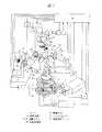
図1は、本発明に係わるパターン欠陥検査装置の一実施の形態を示す図である。本実施の形態において、ウェハ1は、ウェハチャック1aにより、ステージ2の最上面に、たとえば真空吸着などによって固定される。ステージ2は、Yステージ2a、Xステージ2b、θステージ2c、Zステージ2dで構成される。ウェハチャック1aはZステージ2dに固定される。Xステージ2bは定速走行が可能である。Yステージ2aはステップ移動が可能である。θステージ2cは、ウェハチャック1aを回転可能であり、ステージ2の進行方向とウェハ1の傾きを補正可能である。Zステージ2dはウェハ1を上下移動可能である。それぞれの移動は、ステージ制御回路3によって図示しない方法により制御が可能である。 FIG. 1 is a diagram showing an embodiment of a pattern defect inspection apparatus according to the present invention. In the present embodiment, the
照明光源4は、例えば波長355nmや波長266nmの紫外あるいは遠紫外レーザ光源であり、ウェハ1の表面を照明する光源である。このレーザ光源としては、固体YAGレーザを非線形光学結晶等で波長変換して基本波の第3高調波(355nm)や、第4高調波(266nm)を発生する装置で構成される。また、波長193nm、波長195nmあるいは波長248nmなどのレーザ光源を使用しても構わない。さらに、レーザ光源として存在するならば100nm以下の波長でも良く、解像度が益々向上することになる。また、レーザの発振形態は、連続発振でも、パルス発振でも構わないが、ステージ2を連続走行させてウェハ1からの画像を検出する場合は、連続発振が好ましい。パルス発信でも発信周波数の高いものも連続発信レーザと同様に扱うことができる。 The
照明光源4からの光束は、ミラー5,6により照明光学系に導く。NDフィルタ7により、照明光学系に導く光量を調整可能である。NDフィルタ7は図示しない方法によりNDフィルタ制御回路8の指令により駆動可能である。図2によりNDフィルタ7について説明する。(a)はNDフィルタの配置を示した図、(b)はNDフィルタの回転角度と透過率の関係を示した図である。照明光源4からの光束は、レーザの安定化のため、最大出力で照射される。そのため、検査に必要な光量を設定する必要がある。(a)において、照明光源4からの光束はミラー5を反射してNDフィルタ7に通過する。このとき、NDフィルタ7が光束に対して直角であった場合、その反射光は、再度ミラー5を反射して照明光源4の内部に戻ることになる。すると、照明光源4の共振器内でレーザ光が干渉し、レーザ出力が不安定になることになる。 The light beam from the
そこで、NDフィルタ7は光束に足して角度αだけ傾ける。角度αは、NDフィルタ7から反射した光束Rが照明光源4のレーザ出射口に直接戻らない角度に設定すれば良い。NDフィルタ7としては、例えば(b)に示すように透過率が角度によって変化するものを使用する。なおNDフィルタ7は、図示しない方法で回転可能であり、NDフィルタ制御回路8によって所定の角度で固定が可能である。もちろん、透過率を制限した固定NDフィルタを何種類か準備し、これを切り替えても同様に扱うことができる。但し、この状態においても固定NDフィルタは光束に足して角度αだけ傾けるように配置する。 Therefore, the ND filter 7 is inclined by an angle α in addition to the luminous flux. The angle α may be set to an angle at which the light beam R reflected from the ND filter 7 does not return directly to the laser emission port of the
次に、照明光源4からの光束は、ビームエキスパンダ8aにより光束を拡大され、ビームシェイパー9を透過する。図3は一般的な照明光源4の強度分布を示す。通常、レーザの強度分布は中心が高くなるガウシアン分布である。ガウシアン分布では中心の強度分布が極端に強いため、試料面での均一な照度分布を作成するのは困難である。図4にビームシェイパー9を透過後の強度分布を示す。図示しない方法によって、ガウシアン分布を押しつぶすように、明るい部分を平均化が可能である。 Next, the light beam from the
ビームエキスパンダ8aは、図示しない方法によって切り替え制御系8’によって複数の倍率に切り替えることが可能である。もちろん複数の倍率切り替えはズームレンズでも良い。 The
ビームシェイパー9を透過した光束は、ホモジナイザ10を透過したのち、ミラー11、集光レンズ13を透過後、ミラー12よって縦揺動ミラー14に照射される。縦揺動ミラー14は光軸に対して縦方向に移動可能なゴニオステージ16で保持される。縦揺動ミラー14は制御回路15によって制御可能である。ゴニオステージ16は制御回路17によって制御可能である。縦揺動ミラー14で反射した光束は、2個のリレーレンズ18によって横揺動ミラー19で反射される。横揺動ミラー19は光軸に対して横方向に移動可能なゴニオステージ21によって保持される。横揺動ミラー19は制御回路20によって制御可能である。ゴニオステージ21は制御回路22によって制御可能である。 The light beam that has passed through the
横揺動ミラー19で反射した光束は、さらに2個のリレーレンズ23と結像レンズ24を透過し、偏光ビームスプリッタ(以下PBSとする)25によって直角に曲げられ、偏光素子26を透過し、対物レンズ27の瞳28に集光される。すなわち、照明光源4からの光束は前述したレンズ群により、対物レンズ27の瞳28に結像させるケーラ照明を実現している。なお、縦揺動ミラー14と横揺動ミラー19の設置位置はそれぞれ対物レンズ27の集光位置、すなわちウェハ1の表面と共役な関係にあるものとする。 The light beam reflected by the laterally oscillating
回転拡散板29は、レーザによって生じる可干渉性を低減するものである。一般にレーザのようなコヒーレントな光で照明すると、干渉性が高くスペックルノイズと呼ばれる干渉縞が発生し、検出画像にノイズとして表れる。そこで、回転拡散板を照明光路中に挿入し、これを回転させることで、時間的、空間的なコヒーレンシを低減することが可能である。発明者らの実験によると、この回転拡散板29は対物レンズ27の焦点面と共役な位置には配置せず、若干デフォーカスさせることでその効果が得られることが判明している。 The rotating
対物レンズ27としては、屈折型のレンズで説明をしているが、反射型の対物レンズを用いてもよい。PBS25は、照明光の偏光方向が反射面と平行な場合は反射し、垂直な場合は透過する作用を持つ。従って、照明光源にレーザ光を用いると、元々偏光レーザ光であるため、偏光を合わせることによって、PBS25によってこのレーザ光を全反射させることが可能となる。 The
さらに、紫外光による高解像度化に加え、前述したように偏光素子26を図示しない方法によって偏光素子制御回路29aで制御することにより、パターンのコントラストを向上できる。パターンコントラストを向上させるため、偏光素子26の制御によって、紫外レーザ光の偏光状態を自在に制御できることに着目し、照明光の偏光の向き、楕円率を制御し、イメージセンサ35で検出光の一部偏光成分を検出することを可能とした。紫外レーザ光による照明の特徴に単一波長であるということと、直線偏光であるということがある。このため、光路内に設けた偏光素子26を1/2波長板と1/4波長板を組み合わせることで、高効率にその偏光状態を制御することができる。 Furthermore, in addition to increasing the resolution by ultraviolet light, as described above, the
制御は、例えば光軸を中心に1/2波長板と1/4波長板を回転すればよい。試料の形状によっては、照明の偏光状態によりパターンコントラストが大きく変化するため、偏光状態を制御可能(波長板を回転させて位置決め)とすることにより光学系の性能を向上することができる。より具体的には、偏光素子26群の1/2波長板で直線偏光の向きを制御し、1/4波長板で楕円率を変えることができる。これにより、検出感度の向上が図れる。これらの組み合せにより、平行ニコルと直交ニコルも実現できる。もちろん、円偏光状態も実現できる。なお、これらは、照明波長自体には依存しない。 For example, the control may be performed by rotating the half-wave plate and the quarter-wave plate around the optical axis. Depending on the shape of the sample, the pattern contrast changes greatly depending on the polarization state of the illumination. Therefore, the performance of the optical system can be improved by making the polarization state controllable (positioning by rotating the wave plate). More specifically, the direction of linearly polarized light can be controlled by the ½ wavelength plate of the
また、上記概念が成立すれば、実現するための構成は任意のものでよい。もちろん、照明する光学系の対物レンズ27の瞳28と共役な位置に、図示しない空間フィルタを配置し、0次光を減衰させてもよい(空間フィルタにより、パターンからの回折光をブロックし、異物からの散乱光をイメージセンサに導くこともできる)。しかしながら、偏光を制御すると、高次の回折光をより効率的に抽出できる。発明者らの実験によると、約20〜300%コントラストが向上することが判明している。 Moreover, if the said concept is materialized, the structure for implement | achieving may be arbitrary. Of course, a spatial filter (not shown) may be arranged at a position conjugate with the
対物レンズ27の瞳28に集光した光束は、ウェハ1の表面に照明され、その反射光は、再び対物レンズ27によって取り込まれ、偏光素子26、PBS25を透過し、ビームスプリッタ30によって光路を2分岐する。反射した光束は、結像レンズ31によって対物レンズ27の瞳28の像が観察カメラ32に結像されるように配置する。このビームスプリッタ30は、観察カメラ32で必要最小限の光量となるように反射光量を最小限にしている。また、結像レンズ31’によってウェハ1の像が観察カメラ32に結像されるように結像レンズ31’を配置する。結像レンズ31と31’は図示しない方法によってレンズ切り替え制御回路31aによって切り替えが可能である。 The light beam condensed on the
このビームスプリッタ30を透過した光束は、結像レンズ33aと結像レンズ33bによってイメージセンサ35に結像される。このイメージセンサ35はウェハ上換算で、0.05μm〜0.3μm程度の画素寸法を有し、ウェハ1からの反射光の明るさ(濃淡)に応じた濃淡画像信号を出力するものである。ここで、画素寸法に範囲があるのは、結像レンズ33bの倍率を変えれば実現可能である。たとえば、結像レンズ33bの倍率を何種類か搭載し、結像レンズ移動制御系34によって図示しない方法により、所望の倍率にすれば実現できる。もちろん、この結像レンズ33bはズーム機構を持ったレンズでも同様の効果がある。瞳フィルタ41は、対物レンズ27の瞳28と共役な位置に配置されている。この瞳フィルタ41は何種類か搭載し、瞳フィルタ制御系41’によって図示しない方法により切り替えが可能である。 The light beam that has passed through the beam splitter 30 is imaged on the
イメージセンサ35の出力は、ドライバ36を介して画像処理ユニット37に信号が送られる。このドライバ36は、イメージセンサ35の駆動周波数、ゲイン、オフセットなども外部信号によって設定できる構成である。画像処理ユニット37や、その他の制御系は本体制御回路40によってすべての制御が可能である。 The output of the
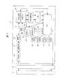
次に、画像処理ユニット37を説明する。図5は、本発明に係わるパターン欠陥検査装置の画像処理ユニット37の一例を示す図である。画像処理ユニット37は、A/D変換器200、階調変換部201、画像フィルタ215、遅延メモリ202、位置合わせ部203、局所階調変換部204、比較部205、CPU212、画像入力部206、散布図作成部207、記憶手段208、表示手段209、出力手段210、および入力手段211等で構成される。 Next, the
イメージセンサ35で得られた濃淡信号は、ドライバ36を介して画像処理ユニット37に送られ、A/D変換器200により、ディジタル画像信号に変換してウェハ1の画像信号を出力するものである。例えば10ビットのものが使われる。階調変換部201は、A/D変換器200から出力される10ビットディジタル画像信号に対して特開平8−320294号公報に記載されたような階調変換を施すものである。すなわち、階調変換部201は、対数変換や指数変換、多項式変換等を施し、画像を補正するものであり、例えば8ビットディジタル信号で出力するように構成される。 The grayscale signal obtained by the
画像フィルタ215は、階調変換され補正された画像から、紫外光で検出された画像の特徴的なノイズを効率良く除去するフィルタである。遅延メモリ202は、参照画像信号を記憶する記憶部であり、画像フィルタ215からの出力画像信号を、繰り返される半導体ウェハを構成する1セル又は複数セルピッチまたは1チップまたは複数チップ分記憶して遅延させるものである。ここで、セルはチップ内のパターンの繰返し単位である。なお、画像フィルタ215は遅延メモリ202を通過した後でもよい。 The
位置合わせ部203は、階調変換部201から出力される階調変換が施された画像信号(試料から得られる検出画像信号)213と遅延メモリ202から得られる遅延画像信号(基準となる参照画像信号)214との位置ずれ量を正規化相関によって検出して画素単位に位置合わせを行なう部分である。 The
局所階調変換部204は、特徴量(明るさ、微分値、標準偏差、テクスチャ等)の異なる信号を、この特徴量が一致するように双方若しくは一方の画像信号について階調変換する部分である。比較部205は、局所階調変換部204で階調変換された検出画像信号同士を比較して特徴量の相違に基いて欠陥を検出する部分である。すなわち、比較部205は、遅延メモリ202から出力されるセルピッチ等に相当する量だけ遅延した参照画像信号と検出した検出画像信号を比較する。 The local
ウェハ1上における配列データ等の座標を、キーボード、ディスク等から構成された入力手段211で入力しておくことにより、CPU212は、ウェハ1上における配列データ等の座標に基づいて、欠陥検査データを作成して記憶手段208に格納する。この欠陥検査データは、必要に応じてディスプレイ等の表示手段209に表示することもでき、また出力手段210に出力することもできる。なお、比較部205の詳細は、特開昭61−212708号公報に示したもの等でよく、例えば画像の位置合わせ回路や、位置合わせされた画像の差画像検出回路、差画像を2値化する不一致検出回路、2値化された出力より面積や長さ(投影長)、座標などを算出する特徴抽出回路からなる。 By inputting the coordinates such as the array data on the
画像入力部206は、位置合わせ部203で画素単位で位置合わせされた両画像の散布図を作成するために、同期あるいは非同期で入力する部分である。散布図作成部207は、画像入力部206で入力された両画像について、カテゴリ別の検出画像の特徴量と参照画像の特徴量との間の散布図を作成し、例えば表示手段209に表示するものである。 The
図6は、本発明に係わるパターン欠陥検査装置における画像処理の流れの一例を示す。画像フィルタ215の一例を説明する。まず、入力された検出画像280と参照画像280’に対し、必要に応じてノイズの除去(281)と画質の改善を行い、S/Nを向上させる。ノイズ除去には各種フィルタが用意され、対象物やノイズの質に応じて選択可能となっている。その例を挙げると、近傍の値を、重みをつけて用いる方法である。実際には着目画素に対してn×mの近傍の値にフィルタ係数をかけて加算するものである。 FIG. 6 shows an example of the flow of image processing in the pattern defect inspection apparatus according to the present invention. An example of the
図7は、本発明に係わるパターン欠陥検査装置における画像処理のフィルタ処理の一例を示す。図7ではm=n=3とし、各近傍画素値の重みが1/8の場合である。着目画素の値は(式1)となる。 FIG. 7 shows an example of image processing filter processing in the pattern defect inspection apparatus according to the present invention. In FIG. 7, m = n = 3, and the weight of each neighboring pixel value is 1/8. The value of the pixel of interest is (Equation 1).

次に、ノイズの除去により劣化した画像を復元(282)する。その1つの例としてウィーナ・フィルタにより復元を行う。これは入力後の画像f(x、y)と復元後の画像f’(x、y)との平均2乗誤差が最小となるような画像を与えるものである。 Next, the image degraded by noise removal is restored (282). As one example, restoration is performed by a Wiener filter. This gives an image in which the mean square error between the input image f (x, y) and the restored image f '(x, y) is minimized.
更に、比較する検出画像と参照画像間で見え方に大きな違いがないかを調べる。評価指標は、コントラスト、明るさのばらつき(標準偏差)、ノイズ成分の周波数などがある。画像間でこれらの特徴に大きな差があればまずは、これらの特徴量を演算(283)し、その後、演算した特徴量を比較(284)して画像の合わせ込み(285)を行う。また、検出処理において、特徴量の合わせ込みができないレベルにあるときは、比較部にて感度を低下させ虚報の発生を押さえるようにする。その後感度低下の判定(286)を行い、結果を表示手段209などに流すものである。なお、画像処理ユニット37での詳細な欠陥算出方法については、特開2001−194323号公報に示したもの等で実現可能である。 Further, it is examined whether there is a large difference in appearance between the detected image to be compared and the reference image. The evaluation index includes contrast, brightness variation (standard deviation), noise component frequency, and the like. If there is a large difference in these features between images, first, these feature amounts are calculated (283), and then the calculated feature amounts are compared (284) to perform image fitting (285). In addition, in the detection process, when the feature amount is at a level that cannot be adjusted, the comparison unit lowers the sensitivity to suppress the generation of false information. Thereafter, a determination of a decrease in sensitivity (286) is performed, and the result is sent to the display means 209 or the like. Note that a detailed defect calculation method in the
次に、ウェハ1に照明する形状について説明する。図8に示すようにイメージセンサとして1次元センサを用いる場合、視野300の全面を照明しても、検出に寄与する照明は領域301だけで、それ以外の光パワーの大部分を占める領域では検出に寄与しないことになる。そこで、照度を向上させるためには、図9に示すように1次元センサに対して領域302のように線状の照明を行うと良いことになる。本発明では、イメージセンサとして、CCDセンサの中でも時間遅延積分形、すなわちTDI(Time Delay &Integration)式のセンサを用いることで構成する。TDIセンサの場合、短手方向には、視野上でN段(数十〜256段程度あるいは10000段程度)のステージと呼ばれる受光部が並び、長手方向にはそのステージが複数個並んで一元センサを形成する。 Next, the shape that illuminates the
この矩形の照明を実現する例を図10を用いて説明する。ホモジナイザ10は、長方形のレンズアレイ304を複数配置したものを使用する。長辺L1と短辺L2の差によって照明される範囲が異なるため、矩形の照明が可能である。L1=L2の場合は円形照明となる。また、レンズアレイ304を複数個配置することによって、瞳上で複数の点光源を実現でき、これを対物レンズ27の瞳28に結像することになるため、ビームシェイパー9と合わせて試料に対して照明むらを抑えられることが可能である。 An example of realizing this rectangular illumination will be described with reference to FIG. The
次に、回転拡散板の説明を行う。回転拡散板29の形状を図11に示す。(a)は、正面図であり、(b)は拡散面の詳細図である。(c)は、(a)の断面X−Xを示したものである。回転拡散板29は、表面から観察すると、粒径が0.1mm程度の大きさで、多角形の形状あるいは円形である粒状704,705,706をランダムに配置して形成することが望ましい。また、断面も粒径に応じ、凹凸の量もランダムな形状をしていることが望ましい。この回転拡散板29をイメージセンサ35の蓄積時間内で高速に回転させることで時間的、空間的なコヒーレンシを低減することができ、光干渉性を無くすことが可能である。 Next, the rotating diffusion plate will be described. The shape of the
高速回転をさせる方法としては、エアータービンモータを用いることで数kHzの回転数を実現することが可能である。しかしながら、数kHzの回転数を実現するためには、回転拡散板29とモータの取り付け状態によっては偏芯が生じて回転時に振動が生じてしまい、装置そのものの精度に影響を及ぼす可能性がある。そこで、回転拡散板29の回転数がイメージセンサ35の蓄積時間に達しなくてもよい低速の回転数で実現可能な方法を提案する。 As a method of rotating at high speed, it is possible to realize a rotational speed of several kHz by using an air turbine motor. However, in order to realize the rotational speed of several kHz, the eccentricity may occur depending on the attachment state of the
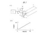
図12に、回転拡散板の回転数と画像ノイズの関係を示す。横軸は回転拡散板の回転数であり、右方向は高速回転に相当する。縦軸は画像ノイズを示し、上方向はノイズが大きいことに相当する。画像ノイズとは、試料上におけるコヒーレンシに相当するものである。実際にイメージセンサ35で画像を取得し、波形707はそのときのランダムノイズを測定したものである。コヒーレンシが大きい場合は、画像ノイズが大きくなることになり、小さい場合は、十分にコヒーレンシが低減されていることに相当する。同図において、回転拡散板の回転数を高速にすると画像ノイズは小さくなっていくことがわかる。画像ノイズは、欠陥判定におけるノイズ以下であればよいため、許容範囲内での回転数を設定すればよいことになる。この回転数は、イメージセンサの蓄積時間の約1/4相当である。 FIG. 12 shows the relationship between the rotational speed of the rotating diffusion plate and image noise. The horizontal axis represents the rotational speed of the rotating diffusion plate, and the right direction corresponds to high-speed rotation. The vertical axis represents image noise, and the upward direction corresponds to a large noise. Image noise corresponds to coherency on a sample. An image is actually acquired by the
また、回転拡散板29の位置に回転位相板を設置しても同様な効果が得られる。図13に回転位相板750の構成を示す。(a)は正面図、(b)は詳細を示した図、(c)は、(a)の断面X−Xを示した図である。位置751では、位相が変化しないような回転位相板750の厚さとする。段差を例えば、段差754では位相差1/2λ、段差752では1/4λ、及び段差753では3/4λ…だけずらして作成する。これらの、深さの異なる多数の段差をランダムに施す。この回転位相板を、回転拡散板29の変わりにモータに固定し、回転させることで、レーザ光の位相を格段の深さに応じて変化させることができるため、レーザの干渉性を低減することが可能である。また、(d)に段差の上面を平坦ではなく突起状にした例を示す。突起の上面をそれぞれ、位置751’では、位相が変化しないような高さとし、段差754’では位相差1/2λ、段差752’では1/4λ、及び段差753’では3/4λ…だけずらして作成する。同様にレーザ光の位相を各段の深さに応じて変化させることができるため、レーザの干渉性を低減することが可能であり、かつ突起の角度が異なるため、光束が拡散する効果もあり、さらなるコヒーレンシの低減が可能である。 A similar effect can be obtained even if a rotational phase plate is installed at the position of the
次に、揺動ミラーについて説明する。図14は、揺動ミラーの配置を示した図である。片側を縦方向に、もう片側を横方法に揺動可能に配置する。縦揺動ミラー14は制御回路15により光軸中心に対して、揺動角度θ1だけ上下に揺動できる。横揺動ミラー19は制御回路20により光軸中心に対して、揺動角度θ2だけ左右に揺動できる。リレーレンズ18により揺動ミラー14,19は同一な共役位置である。 Next, the oscillating mirror will be described. FIG. 14 is a diagram showing the arrangement of the oscillating mirror. One side is arranged so as to be swingable in the vertical direction and the other side in the horizontal direction. The vertical
図15に、揺動ミラーの構造を説明する。揺動ミラー14,19は、固定とする部分と揺動する部分を一体整形して作成される。すなわち、固定側608と609から張り出したバー610,610’によって揺動可能な面607を有する。面607は、コイル611が形成されている。コイル611の両端は、磁石612,613である。コイルに電流614を流すことにより、磁石612,613と反発し、面607が揺動する構造となっている。なお、面607の裏側はレーザ光を全反射するコーティングを施し、ミラーの役目を果たしている。一定の電流を流すと、面607は一定の周波数で揺動することが確認されている。 FIG. 15 illustrates the structure of the oscillating mirror. The swing mirrors 14 and 19 are formed by integrally shaping a fixed part and a swinging part. That is, it has a
図16に、周波数特性を示す。共振周波数を横軸に、揺動角度を縦軸に示す。ピークを持つ周波数は、1000Hzから5000Hzで任意の周波数とする。この周波数を制御するためには、前述したバー610,610’の幅を変えることにより実現可能である。もちろん、1000Hz以下の周波数も可能である。所定の周波数で揺動角度が最大となるような特性で製作する。縦方向、横方向に同じ位相で揺動させるためには、同じ共振周波数の揺動ミラーを使用することが望ましい。 FIG. 16 shows frequency characteristics. The resonance frequency is shown on the horizontal axis, and the swing angle is shown on the vertical axis. The frequency having a peak is an arbitrary frequency from 1000 Hz to 5000 Hz. Controlling this frequency can be realized by changing the width of the above-mentioned
図17に、電流値と揺動角度の関係を示す。電流を横軸に、揺動角度を縦軸に示す。電流を流さない場合は、コイルに電流が流れないため共振しない。そのため、中立の位置で静止する。電流を正、負方向交互に流すことで共振する周波数で揺動することになる。この揺動角度は、電流を制御することで任意に設定可能である。さらに、揺動ミラーの共振周波数は、イメージセンサ35の蓄積時間に同期させることが望ましい。例えば、駆動周波数が300KHzとし、ステージ段数が500段とした場合、600Hzで画像を取得することになる。揺動する共振型の揺動ミラーの周波数が600Hzとなるように特性を設定すれば、蓄積時間で、一回転の揺動が実現可能である。または、共振型の揺動ミラーが製作時のばらつきなどにより、周波数が例えば611Hz等のように理想的な周波数と異なった場合は、イメージセンサの駆動周波数を305.5KHzのように変更すれば、蓄積時間で、一回転の揺動が実現可能である。すなわち、イメージセンサでの画像取得時間と共振型の揺動ミラーの周波数をどちらかで合わすことによって、理想的な揺動と画像取得が可能となる。 FIG. 17 shows the relationship between the current value and the swing angle. The current is plotted on the horizontal axis and the swing angle is plotted on the vertical axis. When no current is passed, no current flows through the coil, so resonance does not occur. Therefore, it stops at the neutral position. Oscillation occurs at a resonating frequency when current is passed alternately in the positive and negative directions. This swing angle can be arbitrarily set by controlling the current. Further, it is desirable that the resonance frequency of the oscillating mirror is synchronized with the accumulation time of the
次に、揺動ミラーの揺動方法について説明する。揺動ミラー14,19はそれぞれ独立した制御が可能である。ここで制御とは揺動角度を示す。 Next, a swinging method of the swinging mirror will be described. The oscillating mirrors 14 and 19 can be independently controlled. Here, the control indicates a swing angle.
まず、縦揺動ミラー14を駆動させ、横揺動ミラー19は静止した状態を説明する。図18は縦揺動ミラー14を制御する例を示す。横軸を時間、縦軸を電流とする。前述したように電流の変化量は揺動角度となる。縦揺動ミラー14に与える電流のパターンを800とする。図19にウェハ1を設置したときに得られる瞳28の観察カメラ32の画像を示す。ウェハ1は鏡面ウェハとする。図18のAの時間では、照明のスポットは瞳28内の最下方801に位置する。時間Bでは同様に最上方802に位置する。時間Cすなわち電流が0の時には瞳中央803に位置することになる。図20に1周期で駆動したときの観察カメラ32の画像を示す。観察カメラの撮像周期は、イメージセンサの駆動周期と一致させた場合と想定する。1駆動周期によってスポット804の形状となる。このスポット804の瞳28の観察カメラの光量分布を図21に示す。(a)は断面A−Aの光量分布、(b)は断面B−Bの光量分布である。揺動方向には移動した範囲で均一な照度分布が得られる。揺動しない方向はスポットに応じた照度分布が得られることになる。 First, the state in which the vertical
次に、横揺動ミラー19を駆動させ、縦揺動ミラー14を静止した状態を説明する。図22は横揺動ミラー19を制御する例を示す。横軸を時間、縦軸を電流とする。横揺動ミラー19に与える電流のパターンを805とする。図23に瞳28の観察カメラ32の画像を示す。図22のAの時間では、照明のスポットは瞳28内の最左方806に位置する。時間Bでは同様に最右方807に位置する。時間Cすなわち電流が0の時には瞳中央808に位置することになる。図24に1周期で駆動したときの観察カメラ32の画像を示す。1駆動周期によってスポット809の形状となる。このスポット809の瞳28の観察カメラの光量分布を図25に示す。(a)は断面A−Aの光量分布、(b)は断面B−Bの光量分布である。揺動方向には移動した範囲で均一な照度分布が得られる。揺動しない方向はスポットに応じた照度分布が得られることになる。すなわち縦揺動ミラー14を揺動したときと90度回転した方向に照度分布が得られることになる。 Next, a state in which the horizontal
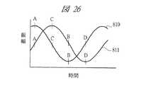
次に、双方の揺動ミラーを同時に駆動したときの状態を説明する。図26は双方の揺動ミラーを制御する例を示す。横軸を時間、縦軸を電流とする。横揺動ミラー19に与える電流のパターンを810、縦揺動ミラー14に与える電流のパターンを811とする。図27に瞳28の観察カメラ32の画像を示す。図26のAの時間では、照明のスポットは瞳内の最右方812に、時間Bでは最下方813に、時間Cでは最左方814に、時間Dでは最上方815にそれぞれ位置することになり、1周期でもとに戻ることになる。図28に1周期で駆動したときの観察カメラ32の画像を示す。スポット816の形状となる。このスポット816の瞳28の観察カメラの光量分布を図29に示す。(a)は断面A−Aの光量分布、(b)は断面B−Bの光量分布である。このようにリング状の照度分布が形成されることになる。 Next, a state when both oscillating mirrors are driven simultaneously will be described. FIG. 26 shows an example of controlling both oscillating mirrors. The horizontal axis is time, and the vertical axis is current. A current pattern applied to the horizontal
この形状は輪帯照明と同じ形状となり、同じ効果が得られることになる。輪帯の形状を変えるためには、揺動ミラーの振幅を換えることによって実現できる。また、静止時のスポット形状の大きさを変えることによって瞳全面に照明できるフラットな照明も実現できることになる。このスポット形状は、ビームエキスパンダ8aの倍率によって決まっているため、このビームエキスパンダ8aの倍率を大きくすれば大きなスポット径が実現でき、小さくすればより小さな輪帯が実現できることになる。ビームエキスパンダ8aの倍率を変えるためには、複数の倍率のビームエキスパンダを切り替えることで実現可能である。また、ビームエキスパンダをズームレンズとすれば、自由な倍率のスポットが実現可能となる。 This shape is the same shape as the annular illumination, and the same effect can be obtained. Changing the shape of the annular zone can be realized by changing the amplitude of the oscillating mirror. Further, it is possible to realize flat illumination that can illuminate the entire pupil surface by changing the size of the spot shape at rest. Since the spot shape is determined by the magnification of the
ビームエキスパンダの倍率を大きくしたときの一例を説明する。図26と同様な制御を行う。図30に瞳28の観察カメラ32の画像を示す。図26のAの時間では、照明のスポットは瞳28内の最右方817に、時間Bでは最下方818に、時間Cでは最左方819に、時間Dでは最上方820にそれぞれ位置することになり、1周期でもとに戻ることになる。図31に1周期で駆動したときの観察カメラ32の画像を示す。スポット821の形状となる。このスポット821の瞳28の観察カメラの光量分布を図32に示す。(a)は断面A−Aの光量分布、(b)は断面B−Bの光量分布である。瞳28全面に一様な照明が実現できる。 An example when the magnification of the beam expander is increased will be described. The same control as in FIG. 26 is performed. FIG. 30 shows an image of the
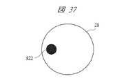
次に、斜方照明について説明する。斜方照明は、揺動ミラーを設置したゴニオステージを制御することで実現可能である。図33に斜方照明を実現する一例の詳細図を示す。図14と同様な構成であるが、揺動ミラーは揺動方向と同じ方向に角度を可変可能なゴニオステージに設置される。片側を縦方向に、もう片側を横方向に揺動可能にゴニオステージを配置する。縦ゴニオステージ16は制御回路17により角度β1に主光線の角度を可変できる。横縦ゴニオステージ21は制御回路22により角度β2に主光線の角度を可変できる。同様にリレーレンズ18により揺動ミラー14、19は同一な共役位置である。なお、揺動ミラー14,19には電流を与えないため中央で静止状態である。図34に双方のゴニオステージが初期位置、すなわち光軸が移動していないときの瞳28の観察カメラ32の画像を示す。照明のスポット822は瞳28内の中央に位置する。この状態は通常の落斜照明である。 Next, oblique illumination will be described. The oblique illumination can be realized by controlling a gonio stage provided with a swing mirror. FIG. 33 shows a detailed view of an example for realizing oblique illumination. Although the configuration is the same as that of FIG. 14, the oscillating mirror is installed on a gonio stage whose angle can be changed in the same direction as the oscillating direction. The gonio stage is arranged so that one side can be swung vertically and the other side can be swung horizontally. The
次に、縦方向に揺動可能なゴニオステージ16を移動した状態を説明する。図33においてβ1を上方向に移動した時には、図35に示すようにスポット822は瞳28内の下方に位置する。また、図33においてβ1を下方向に移動した時には、図36に示すようにスポット822は瞳28内の上方に位置する。 Next, a state where the
同様に、横方向に揺動可能なゴニオステージ21を移動した状態を説明する。図33においてβ2を右方向に移動した時には、図37に示すようにスポット822は瞳28内の左方に位置する。また、図33においてβ1を下方向に移動した時には、図38に示すようにスポット822は瞳28内の右方に位置する。 Similarly, a state where the
このように、主光線を瞳上で斜めから照明することによって斜方照明が実現できることになる。双方の位置を組み合わせることによってさまざまな角度を設定できることになる。 In this way, oblique illumination can be realized by illuminating the chief ray obliquely on the pupil. Various angles can be set by combining both positions.
さらに、揺動ミラーとゴニオステージの位置を組み合わせれば、図39に示すような4重極照明、図40、図41に示すような2重極照明が実現できることはいうまでもない。なお、これらの図は瞳位置での画像である。 Furthermore, it goes without saying that quadrupole illumination as shown in FIG. 39 and double pole illumination as shown in FIGS. 40 and 41 can be realized by combining the positions of the oscillating mirror and the gonio stage. These drawings are images at the pupil position.
なお、共振ミラー、ゴニオステージを制御することによって主光線が移動する方向と瞳の観察カメラにおける方向は、必ずしも本実施の形態の方向と一致するとは限らず、種々の変形が可能であることはいうまでもない。 Note that the direction in which the principal ray moves by controlling the resonant mirror and the gonio stage and the direction of the pupil in the observation camera do not necessarily coincide with the direction of the present embodiment, and various modifications are possible. Needless to say.
また、このような照明方式は、対物レンズに到達するまでの瞳と共役位置にさまざまな遮光フィルタを用いて実現できることはいうまでもない。たとえば、輪帯形状に応じた遮光フィルタを用いれば、本実施の形態と同様に瞳位置で輪帯照明は実現できる。または、ビームエキスパンダ8aのあとに、ビームシェイパー9の変わりに、円錐レンズを組み合わせたコーンレンズのようなものを使用して中心部分の光量を周辺に分散する方法でも輪帯照明は実現できる。 Further, it is needless to say that such an illumination method can be realized by using various light shielding filters at the pupil and the conjugate position until reaching the objective lens. For example, if a light shielding filter corresponding to the annular shape is used, annular illumination can be realized at the pupil position as in the present embodiment. Or after the
図42に、コーンレンズの概念図を示す。コーンレンズ826は円錐レンズ827と828を対向させて配置したものである。図43に入射光の照度分布を示す。横軸にビーム位置、縦軸に光量を示す。このように、中心の強度分布が高い形状となっている。円錐レンズ827の中心付近に入射光をAとすれば、円錐レンズ827によって屈折し、円錐レンズ828の稜線に入射し、出射光Bとして出射光する。図44に出射光の照度分布を示す。横軸にビーム位置、縦軸に光量を示す。このように、周辺の強度分布が高い形状をとり、輪帯照明が実現できる。しかしながら、これらはいずれも照明形状が固定となってしまうことと、照明光を遮光するため、光量不足に陥ることになってしまうことは明らかである。しかし、照明範囲を固定で使用し、照明光量に余裕があり、光量低下を気にしないならば、このような構成においてもなんら問題とならない。 FIG. 42 shows a conceptual diagram of a cone lens. The
次に、ウェハ1の表面と対物レンズ27の焦点位置を常に合わせる一例を説明する。自動焦点系38は対物レンズ27の周辺に設置し、図示しない方法によってウェハ1の高さを検出し、その高さを高さ検出回路39によって計測し、ステージ制御回路3に高さの偏差を入力することでZステージ2dを制御して、常にウェハ1の高さを合せることができる。 Next, an example in which the surface of the
これらの光学系は、図示しない光学架台上に展開し、光源および照明光学系、検出光学系及びイメージセンサなどの光学系を一体化して構成する。その光学架台は、例えば門型のようにし、ステージ2の移動範囲に干渉しないような配置でステージ2を設置した定盤等に設置される。そのため、温度変化、振動等による外乱に対し、安定した検出が可能となる。 These optical systems are developed on an optical mount (not shown), and are configured by integrating optical systems such as a light source, an illumination optical system, a detection optical system, and an image sensor. The optical mount is installed on a surface plate or the like on which the
次に、このようにUV光、特にDUV光を検出できるTDIセンサの一例について説明する。図45に表面反射型センサを示す。照明光源として、DUVレーザ光源を使用する場合は、DUVに対して感度のあるイメージセンサを使用する必要がある。表面照射型イメージセンサ100は、入射光150はカバーガラス151を透過し、ゲート154を通過してCCD155に入るため、短波長の入射光が減衰し400nm以下の波長に対して感度がほとんどなく、DUV光の有効検出はできない。そこで、カバーガラスに有機薄膜コーティングを施し、DUV光が入射されるとそれに応じて可視光を発光するようにすることで、可視光にしか感度のないイメージセンサでDUV光を検出する方法がある。 Next, an example of a TDI sensor capable of detecting UV light, particularly DUV light, will be described. FIG. 45 shows a surface reflection type sensor. When a DUV laser light source is used as the illumination light source, it is necessary to use an image sensor sensitive to DUV. In the front-illuminated
図46に、有機薄膜コーティング方式のイメージセンサを示す。有機薄膜コーティング方式のイメージセンサ101は、カバーガラス151に有機薄膜コーティング152を施し、入射光150の透過光を有機薄膜コーティング面152で蛍光153を発するため、可視光でしか感度のない表面照射形イメージセンサでもDUV光を検出可能となる。 FIG. 46 shows an organic thin film coating type image sensor. In the organic thin film coating
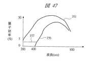
図47に、分光特性を示す。分光特性156は、通常の表面照射型イメージセンサ100の特性である。400nm以下の波長に対して感度なない。分光特性157は、有機薄膜コーティング方式のイメージセンサ101の特性である。400nm以下の波長に対して感度が付加されるようになる。 FIG. 47 shows the spectral characteristics. The spectral characteristic 156 is a characteristic of the normal surface irradiation
さらに、DUV光に対して感度をよくするためには、裏面照射型イメージセンサを使用すればよい。図48に裏面照射型イメージセンサの構造を示す。裏面照射型イメージセンサ102は、入射光150はカバーガラス151を透過して、ゲート構造のない裏側に光が入射する。そのため、ゲート154を通過することがないため、図47に示すように、分光特性161となり、量子効率が高く(例えば、30%以上)ダイナミックレンジが大きくとれ(例えば、3000以上)、400nm以下の波長にも感度があり、200nmを切るような短波長照明に特に有利である。このようなイメージセンサの場合、いくつかの照明波長を用いるときも、ひとつのイメージセンサで対応可能である。また、イメージセンサをTDIにすることで、感度を大きくすることができる。さらに、アンチブルーミングの特性を持たせることで、必要以上の検出光量が得られたときに、周囲の画素に電荷があふれるという課題を解決できる。このように、検査時の波長に最も量子効率のよいイメージセンサを用いることが望ましい。 Furthermore, in order to improve the sensitivity to DUV light, a back-illuminated image sensor may be used. FIG. 48 shows the structure of a back-illuminated image sensor. In the back-illuminated
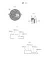
次に、瞳フィルタ41について説明する。図49に瞳フィルタ41の説明図を示す。(a)は形状、(b)は透過率の一例を示す。同図(a)において、中心の遮光部dと周辺の遮光部Dを有する。この透過率は、同図(b)において、中心の遮光部dと周辺の遮光部Dの透過率を変化させる。この形状、透過率を組み合わせたものを何種類か搭載し、試料に応じて最適な条件を見つけ出す。また、この瞳フィルタ41に位相条件を付加するとさらに検出条件が可変可能となる。 Next, the
以上の構成により、動作を説明する。検査時は、ステージ2を走査してウェハ1を等速度で移動させつつ、自動焦点系38で、ウェハ1の被検査面のZ方向位置を図示しない方法で常に検出し、対物レンズ27との間隔が一定になるようにZステージ2dをZ方向に制御する。イメージセンサ35は、ウェハ1上に形成された被検査パターンの明るさ情報(濃淡画像信号)を高精度で検出する。ウェハ1の工程においては、さまざまな材質、表面形状を有しており、それに伴って欠陥部の形状もさまざまな形状をしている。そのため、前述したように、照明条件を変えて検出することによって、条件出しによって所望の欠陥を抽出できる条件を見つけ出せることが可能となる。すなわち、欠陥に対して照射する方向によっては、欠陥部を顕在化できる条件が容易に設定できる。また、検出側の瞳フィルタ41の透過率、位相条件を変えることによって、顕在化された欠陥部の情報をさらに向上できる。 The operation will be described with the above configuration. At the time of inspection, the
図50に、本実施の形態で説明した欠陥検査装置を用いた場合の、半導体形成工程においての有効な活用方法を示す。LSI等の半導体は、さまざまな工程を経て形成される。すなわち、各工程にて転写されたパターンが積層されてデバイスとなるが、その工程のなかで1箇所でも断線、ショートなどの欠陥があるとそれ以降の工程が不良として製作されることになる。この検査装置を用いて、突発的な異常の有無を取得し、それの分析することで、例えば、膜厚装置へのフィードバックが可能となる(400〜404)。また、検出された欠陥部を観察することによって不良解析を行い、致命欠陥でなければ、そのまま工程を通すことで不良率を低減させ、不良であれば製造装置へ速やかにフィードバックをすることで大量の不良を出すことが無くなる(405〜407)。 FIG. 50 shows an effective utilization method in the semiconductor formation process when the defect inspection apparatus described in this embodiment is used. Semiconductors such as LSI are formed through various processes. That is, the pattern transferred in each process is laminated to form a device, but if there is a defect such as disconnection or short-circuit at one place in the process, the subsequent processes are manufactured as defective. By using this inspection apparatus, the presence or absence of a sudden abnormality is acquired and analyzed, and for example, feedback to the film thickness apparatus becomes possible (400 to 404). Also, failure analysis is performed by observing the detected defective part, and if it is not a fatal defect, the defect rate is reduced by passing the process as it is, and if it is defective, a large amount is obtained by prompt feedback to the manufacturing equipment (No. 405 to 407).
図51に、別の実施の形態を示す。対物レンズ27の瞳28と共役位置に照明制限フィルタ43を設置して照明条件を変えることができる一例である。照明制限フィルタ43は複数配置し、図示しない方法によって照明制限フィルタ制御回路44によって照明制限フィルタ43を選択可能である。他の構成は図1と同様である。この照明制限フィルタ43を変えて検出することによって、条件出しによって所望の欠陥を抽出できる条件を見つけ出せることが可能となる。 FIG. 51 shows another embodiment. This is an example in which the illumination condition can be changed by installing an
図52に、さらに別の実施の形態を示す。1次元のイメージセンサをカメラに変えた一例である。カメラ46はコントローラ47によって制御される。カメラ46の画像は、画像処理ユニット37に送られる。他の構成は図1と同様である。検査においては、ステージ2の連続動作であっても、カメラ46のシャッタ時間でステップ動作を行っても同様の画像を取得可能である。このときの揺動ミラーの周波数はカメラ46のシャッタ時間に動機させることが望ましい。 FIG. 52 shows still another embodiment. This is an example in which a one-dimensional image sensor is replaced with a camera. The
また、前記実施の形態においては、明視野光学系を説明したが、検出光学系に共焦点顕微鏡の構成を用いても同様の効果が得られる。 In the above embodiment, the bright field optical system has been described. However, the same effect can be obtained even if the configuration of the confocal microscope is used for the detection optical system.
以上のように構成したパターン欠陥検査装置を用いれば、ウェハの表面に可干渉性を低減させた紫外レーザ光を照射し、この紫外レーザ光が照射されたウェハの表面を撮像して画像信号を得て、この画像信号を処理することによりウェハ上の100nm以下の欠陥を検出し、この検出した100nm以下の欠陥のウェハ上の位置に関する情報を出力することができる。 By using the pattern defect inspection apparatus configured as described above, the surface of the wafer is irradiated with ultraviolet laser light with reduced coherence, and the surface of the wafer irradiated with the ultraviolet laser light is imaged to obtain an image signal. Thus, by processing this image signal, a defect of 100 nm or less on the wafer can be detected, and information on the position of the detected defect of 100 nm or less on the wafer can be output.
また、可干渉性を低減した紫外レーザ光を直径300mm相当のウェハ上に照射し、この照射されたウェハを撮像してウェハの画像を検出し、この検出したウェハの画像を処理してウェハに形成されたパターンの100nm以下の欠陥を1時間あたり3枚以上ウェハのスループットで検出することができる。 In addition, an ultraviolet laser beam having a reduced coherence is irradiated onto a wafer having a diameter of 300 mm, the irradiated wafer is imaged to detect a wafer image, and the detected wafer image is processed to form a wafer. Defects of 100 nm or less in the formed pattern can be detected with a throughput of 3 or more wafers per hour.
特に、このパターン欠陥検査装置を半導体デバイスの製造に用いれば、70nm以下のデザインルールのパターンを検査して半導体デバイスを製造することが可能となる。 In particular, when this pattern defect inspection apparatus is used for manufacturing a semiconductor device, it is possible to manufacture a semiconductor device by inspecting a design rule pattern of 70 nm or less.
1…ウェハ、1a…ウェハチャック、2…ステージ、2a…Yステージ、2b…Xステージ、2c…θステージ、2d…Zステージ、3…ステージ制御回路、4…照明光源、5,6…ミラー、7…NDフィルタ、8…NDフィルタ制御回路、8’…切り替え制御系、8a…ビームエキスパンダ、9…ビームシェイパー、10…ホモジナイザ、11,12…ミラー、13…集光レンズ、14,19…揺動ミラー、15,17…制御回路、16,21…ゴニオステージ、18…リレーレンズ、20,22…制御回路、23…リレーレンズ、24…結像レンズ、25…偏光ビームスプリッタ、26…偏光素子、27…対物レンズ、28…瞳、29…回転拡散板、29a…偏光素子制御回路、30…ビームスプリッタ、31,31’…結像レンズ、31a…レンズ切り替え制御回路、32…観察カメラ、33a,33b…結像レンズ、34…結像レンズ移動制御系、35…イメージセンサ、36…ドライバ、37…画像処理ユニット、38…自動焦点系、39…高さ検出回路、40…制御回路、41…瞳フィルタ、41’…瞳フィルタ制御系、43…照明制限フィルタ、44…照明制限フィルタ制御回路、46…カメラ、47…コントローラ、200…A/D変換器、201…階調変換部、202…遅延メモリ、203…位置合わせ部、204…局所階調変換部、205…比較部、206…画像入力部、207…散布図作成部、208…記憶手段、209…表示手段、210…出力手段、211…入力手段、212…CPU、215…画像フィルタ。 DESCRIPTION OF
Claims (7)
Translated fromJapanese前記照明光源は、レーザあるいはランプであり、波長が365nmから193nmの範囲であることを特徴とするパターン欠陥検査装置。The pattern defect inspection apparatus according to claim 1,
The illumination light source is a laser or a lamp and has a wavelength in the range of 365 nm to 193 nm.
前記光量調整手段は、前記光量を低減可能なフィルタと、前記フィルタによって任意の透過光量を設定可能な光量設定系とを備え、
前記フィルタは、光軸を傾けて該フィルタからの反射光を光源に直接戻さないように設置されていることを特徴とするパターン欠陥検査装置。The pattern defect inspection apparatus according to claim 1,
The light amount adjusting means includes a filter capable of reducing the light amount, and a light amount setting system capable of setting an arbitrary transmitted light amount by the filter,
The pattern defect inspection apparatus according to claim 1, wherein the filter is installed so as to tilt the optical axis so that the reflected light from the filter does not return directly to the light source.
前記照明手段は、前記光束を瞳内で自在に移動かつ静止可能であり、前記試料と共役な位置で移動するように構成されていることを特徴とするパターン欠陥検査装置。The pattern defect inspection apparatus according to claim 1,
The pattern defect inspection apparatus, wherein the illuminating means is configured to move and stop the light beam freely in a pupil and to move at a position conjugate with the sample.
前記画像検出手段は、蓄積型のイメージセンサ、または紫外光に対して感度を有する時間遅延積分型(TDI)のイメージセンサを有して構成され、
前記時間遅延積分型(TDI)のイメージセンサは、アンチブルーミングTDIセンサ、カバーガラスに有機薄膜コーティングを施した表面照射型TDIセンサ、あるいは裏面照射型TDIセンサであることを特徴とするパターン欠陥検査装置。The pattern defect inspection apparatus according to claim 1,
The image detecting means includes a storage type image sensor or a time delay integration type (TDI) image sensor having sensitivity to ultraviolet light,
The time delay integration type (TDI) image sensor is an anti-blooming TDI sensor, a surface irradiation type TDI sensor having a cover glass coated with an organic thin film, or a back side irradiation type TDI sensor. .
前記欠陥検出手段は、参照画像信号を記憶する記憶部と、前記画像検出手段から検出される検出画像信号の正常部における特徴量と前記記憶部に記憶された参照画像信号の正常部における特徴量との対応関係を示す散布図を作成する散布図作成部と、前記散布図作成部で作成された散布図に基いて画像信号の階調値を補正する階調変換部と、前記階調変換部で補正された検出画像信号と前記参照画像信号とを比較することにより前記試料に形成されたパターンの欠陥を検出する欠陥検出部とを備えることを特徴とするパターン欠陥検査装置。The pattern defect inspection apparatus according to claim 1,
The defect detection unit includes a storage unit that stores a reference image signal, a feature amount in a normal part of the detected image signal detected from the image detection unit, and a feature amount in a normal part of the reference image signal stored in the storage unit A scatter diagram creating unit for creating a scatter diagram showing a correspondence relationship between the image, a gradation converting unit for correcting a gradation value of an image signal based on the scatter diagram created by the scatter diagram creating unit, and the gradation conversion A pattern defect inspection apparatus comprising: a defect detection unit that detects a defect of a pattern formed on the sample by comparing the detection image signal corrected by the unit and the reference image signal.
前記欠陥検出手段は、検出するパターンの欠陥についての位置及び寸法に関する情報を出力するように構成されていることを特徴とするパターン欠陥検査装置。The pattern defect inspection apparatus according to claim 1,
The pattern defect inspection apparatus, wherein the defect detection means is configured to output information related to a position and a dimension regarding a defect of a pattern to be detected.
Priority Applications (2)
| Application Number | Priority Date | Filing Date | Title |
|---|---|---|---|
| JP2003325526AJP4260587B2 (en) | 2003-09-18 | 2003-09-18 | Pattern defect inspection system |
| US10/914,115US7295305B2 (en) | 2003-09-18 | 2004-08-10 | Method and its apparatus for inspecting a pattern |
Applications Claiming Priority (1)
| Application Number | Priority Date | Filing Date | Title |
|---|---|---|---|
| JP2003325526AJP4260587B2 (en) | 2003-09-18 | 2003-09-18 | Pattern defect inspection system |
Publications (2)
| Publication Number | Publication Date |
|---|---|
| JP2005091182A JP2005091182A (en) | 2005-04-07 |
| JP4260587B2true JP4260587B2 (en) | 2009-04-30 |
Family
ID=34308705
Family Applications (1)
| Application Number | Title | Priority Date | Filing Date |
|---|---|---|---|
| JP2003325526AExpired - Fee RelatedJP4260587B2 (en) | 2003-09-18 | 2003-09-18 | Pattern defect inspection system |
Country Status (2)
| Country | Link |
|---|---|
| US (1) | US7295305B2 (en) |
| JP (1) | JP4260587B2 (en) |
Families Citing this family (39)
| Publication number | Priority date | Publication date | Assignee | Title |
|---|---|---|---|---|
| KR100734751B1 (en) | 2005-04-28 | 2007-07-03 | 에버테크노 주식회사 | Jig for small polarizing film inspection |
| US7548308B2 (en)* | 2005-05-11 | 2009-06-16 | Kla-Tencor Corporation | Illumination energy management in surface inspection |
| US7609373B2 (en)* | 2005-05-31 | 2009-10-27 | Kla-Tencor Technologies Corporation | Reducing variations in energy reflected from a sample due to thin film interference |
| US9037280B2 (en)* | 2005-06-06 | 2015-05-19 | Kla-Tencor Technologies Corp. | Computer-implemented methods for performing one or more defect-related functions |
| US7570800B2 (en)* | 2005-12-14 | 2009-08-04 | Kla-Tencor Technologies Corp. | Methods and systems for binning defects detected on a specimen |
| US20090080194A1 (en)* | 2006-02-15 | 2009-03-26 | Li-Cor, Inc. | Fluorescence filtering system and method for molecular imaging |
| US7664608B2 (en)* | 2006-07-14 | 2010-02-16 | Hitachi High-Technologies Corporation | Defect inspection method and apparatus |
| US7894659B2 (en)* | 2007-02-28 | 2011-02-22 | Kla-Tencor Technologies Corp. | Methods for accurate identification of an edge of a care area for an array area formed on a wafer and methods for binning defects detected in an array area formed on a wafer |
| US7925072B2 (en)* | 2007-03-08 | 2011-04-12 | Kla-Tencor Technologies Corp. | Methods for identifying array areas in dies formed on a wafer and methods for setting up such methods |
| JP2009076669A (en)* | 2007-09-20 | 2009-04-09 | Fujitsu Ltd | Active layer evaluation method and optical semiconductor device manufacturing method |
| US7843558B2 (en)* | 2008-06-25 | 2010-11-30 | Applied Materials South East Asia Pte. Ltd. | Optical inspection tools featuring light shaping diffusers |
| JP5526370B2 (en)* | 2009-11-02 | 2014-06-18 | レーザーテック株式会社 | Illumination optical system, illumination method, and inspection apparatus |
| JP2012047654A (en)* | 2010-08-30 | 2012-03-08 | Hitachi High-Technologies Corp | Defect inspection device and defect inspection method |
| DE102011121532A1 (en) | 2010-12-23 | 2012-06-28 | Carl Zeiss Sms Gmbh | Method for characterizing a structure on a mask and device for carrying out the method |
| US9503606B2 (en) | 2011-09-28 | 2016-11-22 | Semiconductor Components Industries, Llc | Time-delay-and-integrate image sensors having variable integration times |
| JP5851784B2 (en)* | 2011-09-28 | 2016-02-03 | 株式会社ディスコ | Height position detector and laser processing machine |
| US8614790B2 (en)* | 2011-12-12 | 2013-12-24 | Applied Materials Israel, Ltd. | Optical system and method for inspection of patterned samples |
| US9128064B2 (en) | 2012-05-29 | 2015-09-08 | Kla-Tencor Corporation | Super resolution inspection system |
| JP5921990B2 (en)* | 2012-08-23 | 2016-05-24 | 株式会社ニューフレアテクノロジー | Defect detection method |
| JP6039314B2 (en)* | 2012-08-30 | 2016-12-07 | キヤノン株式会社 | Imaging apparatus and imaging method |
| US8948494B2 (en) | 2012-11-12 | 2015-02-03 | Kla-Tencor Corp. | Unbiased wafer defect samples |
| KR102044864B1 (en)* | 2012-12-13 | 2019-12-06 | 삼성디스플레이 주식회사 | Laser patterning examing apparatus |
| JP6142996B2 (en)* | 2013-06-26 | 2017-06-07 | レーザーテック株式会社 | Via shape measuring device and via inspection device |
| CN103575741A (en)* | 2013-10-29 | 2014-02-12 | 浚丰太阳能(江苏)有限公司 | Bottom surface appearance inspector |
| CN105684081A (en)* | 2013-11-08 | 2016-06-15 | 株式会社日立制作所 | Holographic storage device |
| CN103913466A (en)* | 2014-04-08 | 2014-07-09 | 上海华力微电子有限公司 | Detection device and detection method for wafer defect |
| US9541750B2 (en) | 2014-06-23 | 2017-01-10 | Li-Cor, Inc. | Telecentric, wide-field fluorescence scanning systems and methods |
| KR20160081423A (en)* | 2014-12-31 | 2016-07-08 | 삼성전자주식회사 | Method and system for defecting defect |
| RU2650733C2 (en)* | 2016-10-03 | 2018-04-17 | Федеральное государственное бюджетное образовательное учреждение высшего образования "Кубанский государственный технологический университет" (ФГБОУ ВО "КубГТУ") | Controller of estimation and prediction of storability of objects with structural inhomogeneity |
| JP6953242B2 (en)* | 2017-09-06 | 2021-10-27 | 株式会社ディスコ | Height detector and laser machining equipment |
| JP6768622B2 (en)* | 2017-09-28 | 2020-10-14 | 株式会社ニューフレアテクノロジー | Inspection method and inspection equipment |
| KR20190041163A (en)* | 2017-10-12 | 2019-04-22 | 삼성전자주식회사 | A system and method for oprical testing and method for fabricating using the system and method for oprical testing |
| US10572989B2 (en)* | 2018-06-06 | 2020-02-25 | The Boeing Company | Chopped fiber additive manufacturing void detection |
| US11784077B2 (en) | 2019-12-18 | 2023-10-10 | Micron Technology, Inc. | Wafer overlay marks, overlay measurement systems, and related methods |
| CN113452347B (en)* | 2021-05-14 | 2024-08-30 | 北京和崎精密科技有限公司 | Signal fuzzy control filter for wafer detection device |
| KR20250093551A (en)* | 2023-03-17 | 2025-06-24 | 야마하하쓰도키 가부시키가이샤 | Inspection device and inspection method |
| CN116091500B (en)* | 2023-04-07 | 2023-07-04 | 成都数之联科技股份有限公司 | Diffuser plate defect detection method, model training method, device, equipment and medium |
| CN116958793B (en)* | 2023-07-24 | 2024-08-27 | 国网江苏省电力有限公司泰州供电分公司 | Device and method for evaluating visual recognition of charging robot based on illumination condition |
| US20250044679A1 (en)* | 2023-07-31 | 2025-02-06 | Kla Corporation | Pupil filter with spatially-varying transmission |
Family Cites Families (14)
| Publication number | Priority date | Publication date | Assignee | Title |
|---|---|---|---|---|
| JPS59226317A (en) | 1983-06-06 | 1984-12-19 | Nippon Kogaku Kk <Nikon> | Illuminating device |
| JPH0624180B2 (en) | 1986-04-02 | 1994-03-30 | 株式会社日立製作所 | Projection exposure method and apparatus thereof |
| JP3346032B2 (en) | 1994-05-30 | 2002-11-18 | 株式会社日立製作所 | Pattern inspection apparatus and method |
| US5774222A (en)* | 1994-10-07 | 1998-06-30 | Hitachi, Ltd. | Manufacturing method of semiconductor substrative and method and apparatus for inspecting defects of patterns on an object to be inspected |
| JP3279868B2 (en) | 1995-05-26 | 2002-04-30 | 株式会社日立製作所 | Defect inspection method and device for inspected pattern |
| US6288780B1 (en)* | 1995-06-06 | 2001-09-11 | Kla-Tencor Technologies Corp. | High throughput brightfield/darkfield wafer inspection system using advanced optical techniques |
| JPH1078668A (en) | 1996-09-04 | 1998-03-24 | Toshiba Corp | Inspection device |
| JPH1183753A (en)* | 1997-07-09 | 1999-03-26 | Toshiba Corp | Optical board inspection equipment |
| JPH11183393A (en)* | 1997-10-13 | 1999-07-09 | Mitsubishi Electric Corp | Pattern defect inspection apparatus and pattern defect inspection method |
| JP4009409B2 (en)* | 1999-10-29 | 2007-11-14 | 株式会社日立製作所 | Pattern defect inspection method and apparatus |
| US6621571B1 (en)* | 1999-10-29 | 2003-09-16 | Hitachi, Ltd. | Method and apparatus for inspecting defects in a patterned specimen |
| US6369888B1 (en)* | 1999-11-17 | 2002-04-09 | Applied Materials, Inc. | Method and apparatus for article inspection including speckle reduction |
| JP2003177102A (en)* | 2001-09-13 | 2003-06-27 | Hitachi Ltd | Pattern defect inspection method and apparatus |
| US6900888B2 (en)* | 2001-09-13 | 2005-05-31 | Hitachi High-Technologies Corporation | Method and apparatus for inspecting a pattern formed on a substrate |
- 2003
- 2003-09-18JPJP2003325526Apatent/JP4260587B2/ennot_activeExpired - Fee Related
- 2004
- 2004-08-10USUS10/914,115patent/US7295305B2/ennot_activeExpired - Fee Related
Also Published As
| Publication number | Publication date |
|---|---|
| US20050062963A1 (en) | 2005-03-24 |
| US7295305B2 (en) | 2007-11-13 |
| JP2005091182A (en) | 2005-04-07 |
Similar Documents
| Publication | Publication Date | Title |
|---|---|---|
| JP4260587B2 (en) | Pattern defect inspection system | |
| US7463350B2 (en) | Method and apparatus for detecting defects of a sample using a dark field signal and a bright field signal | |
| JP4009409B2 (en) | Pattern defect inspection method and apparatus | |
| US6556290B2 (en) | Defect inspection method and apparatus therefor | |
| US7205549B2 (en) | Pattern defect inspection method and its apparatus | |
| US6900888B2 (en) | Method and apparatus for inspecting a pattern formed on a substrate | |
| US7489395B2 (en) | Method and apparatus for inspecting pattern defects | |
| TW202208812A (en) | Measurement modes for overlay | |
| KR102335198B1 (en) | Extreme ultraviolet (euv) substrate inspection system with simplified optics and method of manufacturing thereof | |
| JP5303217B2 (en) | Defect inspection method and defect inspection apparatus | |
| US20060012780A1 (en) | Method and apparatus for inspecting pattern defects | |
| JP2004264287A (en) | Method and apparatus for identifying defect in substrate surface using dithering for reconstructing image of insufficient sampling | |
| JP5571969B2 (en) | Defect inspection method and apparatus | |
| JP2003177102A (en) | Pattern defect inspection method and apparatus | |
| JP3956942B2 (en) | Defect inspection method and apparatus | |
| US7738092B1 (en) | System and method for reducing speckle noise in die-to-die inspection systems | |
| JP3752935B2 (en) | Pattern defect inspection method and apparatus | |
| JP2002090313A (en) | Pattern defect inspection equipment |
Legal Events
| Date | Code | Title | Description |
|---|---|---|---|
| A711 | Notification of change in applicant | Free format text:JAPANESE INTERMEDIATE CODE: A711 Effective date:20050317 | |
| A621 | Written request for application examination | Free format text:JAPANESE INTERMEDIATE CODE: A621 Effective date:20051102 | |
| A977 | Report on retrieval | Free format text:JAPANESE INTERMEDIATE CODE: A971007 Effective date:20080527 | |
| A131 | Notification of reasons for refusal | Free format text:JAPANESE INTERMEDIATE CODE: A131 Effective date:20080603 | |
| A521 | Written amendment | Free format text:JAPANESE INTERMEDIATE CODE: A523 Effective date:20080731 | |
| A131 | Notification of reasons for refusal | Free format text:JAPANESE INTERMEDIATE CODE: A131 Effective date:20081007 | |
| A521 | Written amendment | Free format text:JAPANESE INTERMEDIATE CODE: A523 Effective date:20081204 | |
| TRDD | Decision of grant or rejection written | ||
| A01 | Written decision to grant a patent or to grant a registration (utility model) | Free format text:JAPANESE INTERMEDIATE CODE: A01 Effective date:20090106 | |
| A01 | Written decision to grant a patent or to grant a registration (utility model) | Free format text:JAPANESE INTERMEDIATE CODE: A01 | |
| A61 | First payment of annual fees (during grant procedure) | Free format text:JAPANESE INTERMEDIATE CODE: A61 Effective date:20090204 | |
| FPAY | Renewal fee payment (event date is renewal date of database) | Free format text:PAYMENT UNTIL: 20120220 Year of fee payment:3 | |
| R150 | Certificate of patent or registration of utility model | Free format text:JAPANESE INTERMEDIATE CODE: R150 | |
| FPAY | Renewal fee payment (event date is renewal date of database) | Free format text:PAYMENT UNTIL: 20120220 Year of fee payment:3 | |
| FPAY | Renewal fee payment (event date is renewal date of database) | Free format text:PAYMENT UNTIL: 20130220 Year of fee payment:4 | |
| FPAY | Renewal fee payment (event date is renewal date of database) | Free format text:PAYMENT UNTIL: 20130220 Year of fee payment:4 | |
| FPAY | Renewal fee payment (event date is renewal date of database) | Free format text:PAYMENT UNTIL: 20140220 Year of fee payment:5 | |
| LAPS | Cancellation because of no payment of annual fees |