JP4260126B2 - Color organic EL display device - Google Patents
Color organic EL display deviceDownload PDFInfo
- Publication number
- JP4260126B2 JP4260126B2JP2005070782AJP2005070782AJP4260126B2JP 4260126 B2JP4260126 B2JP 4260126B2JP 2005070782 AJP2005070782 AJP 2005070782AJP 2005070782 AJP2005070782 AJP 2005070782AJP 4260126 B2JP4260126 B2JP 4260126B2
- Authority
- JP
- Japan
- Prior art keywords
- organic
- light emitting
- color
- display device
- light
- Prior art date
- Legal status (The legal status is an assumption and is not a legal conclusion. Google has not performed a legal analysis and makes no representation as to the accuracy of the status listed.)
- Expired - Lifetime
Links
- 230000005525hole transportEffects0.000claimsdescription27
- 239000011368organic materialSubstances0.000claimsdescription2
- 230000007423decreaseEffects0.000claims1
- 239000010410layerSubstances0.000description100
- 239000010408filmSubstances0.000description43
- 239000000463materialSubstances0.000description20
- 239000000758substrateSubstances0.000description18
- 239000003990capacitorSubstances0.000description13
- 238000000034methodMethods0.000description11
- 238000003860storageMethods0.000description9
- 229910017911MgInInorganic materials0.000description8
- 239000011229interlayerSubstances0.000description7
- 239000003086colorantSubstances0.000description6
- 229910004298SiO 2Inorganic materials0.000description5
- 239000011651chromiumSubstances0.000description4
- 229910052751metalInorganic materials0.000description4
- 239000002184metalSubstances0.000description4
- 229910045601alloyInorganic materials0.000description3
- 239000000956alloySubstances0.000description3
- 230000015572biosynthetic processEffects0.000description3
- 229910052804chromiumInorganic materials0.000description3
- 238000000151depositionMethods0.000description3
- 230000000694effectsEffects0.000description3
- 239000011521glassSubstances0.000description3
- 239000011159matrix materialSubstances0.000description3
- 150000002894organic compoundsChemical class0.000description3
- 230000002093peripheral effectEffects0.000description3
- VYZAMTAEIAYCRO-UHFFFAOYSA-NChromiumChemical compound[Cr]VYZAMTAEIAYCRO-UHFFFAOYSA-N0.000description2
- 229910000846In alloyInorganic materials0.000description2
- VYPSYNLAJGMNEJ-UHFFFAOYSA-NSilicium dioxideChemical compoundO=[Si]=OVYPSYNLAJGMNEJ-UHFFFAOYSA-N0.000description2
- HCHKCACWOHOZIP-UHFFFAOYSA-NZincChemical compound[Zn]HCHKCACWOHOZIP-UHFFFAOYSA-N0.000description2
- JHYLKGDXMUDNEO-UHFFFAOYSA-N[Mg].[In]Chemical compound[Mg].[In]JHYLKGDXMUDNEO-UHFFFAOYSA-N0.000description2
- 239000003513alkaliSubstances0.000description2
- 238000005530etchingMethods0.000description2
- 229910052750molybdenumInorganic materials0.000description2
- 239000003870refractory metalSubstances0.000description2
- 229920005989resinPolymers0.000description2
- 239000011347resinSubstances0.000description2
- 239000004065semiconductorSubstances0.000description2
- 238000004904shorteningMethods0.000description2
- 238000004544sputter depositionMethods0.000description2
- 238000007740vapor depositionMethods0.000description2
- 229910052725zincInorganic materials0.000description2
- 239000011701zincSubstances0.000description2
- SSSJRLUYNHCGEB-UHFFFAOYSA-N1-n',1-n'-bis(3-methylphenyl)-4-phenylcyclohexa-2,4-diene-1,1-diamineChemical compoundCC1=CC=CC(N(C=2C=C(C)C=CC=2)C2(N)C=CC(=CC2)C=2C=CC=CC=2)=C1SSSJRLUYNHCGEB-UHFFFAOYSA-N0.000description1
- BTEAMLUWLVUBFF-UHFFFAOYSA-N5-(3-methylphenyl)-4-phenylcyclohexa-2,4-diene-1,1-diamineChemical compoundCC=1C=C(C=CC1)C1=C(C=CC(C1)(N)N)C1=CC=CC=C1BTEAMLUWLVUBFF-UHFFFAOYSA-N0.000description1
- ZOKXTWBITQBERF-UHFFFAOYSA-NMolybdenumChemical compound[Mo]ZOKXTWBITQBERF-UHFFFAOYSA-N0.000description1
- NRCMAYZCPIVABH-UHFFFAOYSA-NQuinacridoneChemical classN1C2=CC=CC=C2C(=O)C2=C1C=C1C(=O)C3=CC=CC=C3NC1=C2NRCMAYZCPIVABH-UHFFFAOYSA-N0.000description1
- XUIMIQQOPSSXEZ-UHFFFAOYSA-NSiliconChemical compound[Si]XUIMIQQOPSSXEZ-UHFFFAOYSA-N0.000description1
- 229910052790berylliumInorganic materials0.000description1
- ATBAMAFKBVZNFJ-UHFFFAOYSA-Nberyllium atomChemical compound[Be]ATBAMAFKBVZNFJ-UHFFFAOYSA-N0.000description1
- GQVWHWAWLPCBHB-UHFFFAOYSA-Lberyllium;benzo[h]quinolin-10-olateChemical compound[Be+2].C1=CC=NC2=C3C([O-])=CC=CC3=CC=C21.C1=CC=NC2=C3C([O-])=CC=CC3=CC=C21GQVWHWAWLPCBHB-UHFFFAOYSA-L0.000description1
- 150000001875compoundsChemical class0.000description1
- 230000009849deactivationEffects0.000description1
- 230000006866deteriorationEffects0.000description1
- 238000005401electroluminescenceMethods0.000description1
- 238000001704evaporationMethods0.000description1
- AMGQUBHHOARCQH-UHFFFAOYSA-Nindium;oxotinChemical compound[In].[Sn]=OAMGQUBHHOARCQH-UHFFFAOYSA-N0.000description1
- 239000011810insulating materialSubstances0.000description1
- 238000010030laminatingMethods0.000description1
- 230000014759maintenance of locationEffects0.000description1
- 238000004519manufacturing processMethods0.000description1
- 239000011733molybdenumSubstances0.000description1
- JNDYNKXUHHOEKB-UHFFFAOYSA-Nn,n-dimethyl-4-(5-phenyl-1,3,4-oxadiazol-2-yl)anilineChemical compoundC1=CC(N(C)C)=CC=C1C1=NN=C(C=2C=CC=CC=2)O1JNDYNKXUHHOEKB-UHFFFAOYSA-N0.000description1
- 229920003217poly(methylsilsesquioxane)Polymers0.000description1
- 229910021420polycrystalline siliconInorganic materials0.000description1
- 230000005855radiationEffects0.000description1
- 229910052710siliconInorganic materials0.000description1
- 239000010703siliconSubstances0.000description1
- 239000002356single layerSubstances0.000description1
- 229920003002synthetic resinPolymers0.000description1
- 239000000057synthetic resinSubstances0.000description1
- 239000010409thin filmSubstances0.000description1
- WFKWXMTUELFFGS-UHFFFAOYSA-NtungstenChemical compound[W]WFKWXMTUELFFGS-UHFFFAOYSA-N0.000description1
- 229910052721tungstenInorganic materials0.000description1
- 239000010937tungstenSubstances0.000description1
Images


Classifications
- H—ELECTRICITY
- H10—SEMICONDUCTOR DEVICES; ELECTRIC SOLID-STATE DEVICES NOT OTHERWISE PROVIDED FOR
- H10K—ORGANIC ELECTRIC SOLID-STATE DEVICES
- H10K59/00—Integrated devices, or assemblies of multiple devices, comprising at least one organic light-emitting element covered by group H10K50/00
- H10K59/30—Devices specially adapted for multicolour light emission
- H10K59/35—Devices specially adapted for multicolour light emission comprising red-green-blue [RGB] subpixels
- H10K59/352—Devices specially adapted for multicolour light emission comprising red-green-blue [RGB] subpixels the areas of the RGB subpixels being different
Landscapes
- Electroluminescent Light Sources (AREA)
- Devices For Indicating Variable Information By Combining Individual Elements (AREA)
Description
Translated fromJapanese本発明は、エレクトロルミネッセンス(Electroluminescence:以下、「EL」と称する。)素子等の自発光素子、及び薄膜トランジスタ(Thin Film Transistor:以下、「TFT」と称する。)を備えたカラー有機EL表示装置に関する。 The present invention relates to a color organic EL display device including a self-luminous element such as an electroluminescence (hereinafter referred to as “EL”) element and a thin film transistor (hereinafter referred to as “TFT”). .
近年、EL素子を用いたEL表示装置が、CRTやLCDに代わる表示装置として注目されている。 In recent years, an EL display device using an EL element has attracted attention as a display device that replaces a CRT or an LCD.
また、そのEL素子を駆動させるスイッチング素子としてTFTを備えた表示装置も研究開発されている。 In addition, a display device including a TFT as a switching element for driving the EL element has been researched and developed.
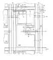
図7に有機EL表示装置の表示画素付近を示す平面図を示し、図8(a)に図7中のA−A線に沿った断面図を示し、図8(b)に図7中のB−B線に沿った断面図を示す。 FIG. 7 is a plan view showing the vicinity of the display pixel of the organic EL display device, FIG. 8A is a cross-sectional view taken along the line AA in FIG. 7, and FIG. Sectional drawing along a BB line is shown.
図7に示すように、ゲート信号線51とドレイン信号線52とに囲まれた領域に表示画素が形成されている。両信号線の交点付近には第1のTFT30が備えられており、そのTFT30のソース13sは後述の保持容量電極線54との間で容量をなす容量電極55を兼ねるとともに、第2のTFT40のゲート41に接続されている。第2のTFTのソース43sは有機EL素子60の陽極61に接続され、他方のドレイン43dは有機EL素子60に供給される電流源である駆動電源線53に接続されている。 As shown in FIG. 7, display pixels are formed in a region surrounded by the
また、TFTの付近には、ゲート信号線51と並行に保持容量電極線54が配置されている。この保持容量電極線54はクロム等から成っている。また、保持容量電極線54は、TFT30のソース13sに接続された容量電極55とはゲート絶縁膜12を介して形成されている。そして、保持容量電極線54と容量電極55との間で電荷を蓄積して容量を成している。この保持容量は、第2のTFT40のゲート電極41に印加される電圧を保持するために設けられている。 In addition, a storage
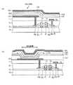
図8に示すように、有機EL表示装置は、ガラスや合成樹脂などから成る基板又は導電性を有する基板あるいは半導体基板等の基板10上に、TFT及び有機EL素子を順に積層形成して成る。ただし、基板10として導電性を有する基板及び半導体基板を用いる場合には、これらの基板10上にSiO2やSiNなどの絶縁膜を形成した上にTFT及び有機EL素子を形成する。As shown in FIG. 8, the organic EL display device is formed by sequentially laminating TFTs and organic EL elements on a
まず、スイッチング用のTFTである第1のTFT30について説明する。 First, the
図8(a)に示すように、石英ガラス、無アルカリガラス等からなる絶縁性基板10上に、クロム(Cr)、モリブデン(Mo)などの高融点金属からなるゲート電極11を兼ねたゲート信号線51及び保持容量電極線54を配置する。続いて、ゲート絶縁膜12、及び多結晶シリコン(以下、「p−Si」と称する。)膜からなる能動層13が順に積層されている。 As shown in FIG. 8A, a gate signal also serving as a
そして、ゲート絶縁膜12、能動層13及びストッパ絶縁膜14上の全面には、SiO2膜、SiN膜及びSiO2膜の順に積層された層間絶縁膜15が形成されており、この層間絶縁膜15のドレイン13dに対応する位置に形成したコンタクトホールに、Al等の金属を充填したドレイン電極16が設けられ、更に基板全面に有機樹脂から成り表面を平
坦にする平坦化絶縁膜17が形成されている。An
次に、有機EL素子の駆動用のTFTである第2のTFT40について説明する。 Next, the
図8(b)に示すように、石英ガラス、無アルカリガラス等からなる絶縁性基板10上に、Cr、Moなどの高融点金属からなるゲート電極41、ゲート絶縁膜12、及びp−Si膜からなる能動層43を順に形成されており、その能動層43には、チャネル43cと、このチャネル43cの両側にソース43s及びドレイン43dが設けられている。そして、ゲート絶縁膜12及び能動層43上の全面に、SiO2膜、SiN膜及びSiO2膜の順に積層された層間絶縁膜15を形成し、この層間絶縁膜15のドレイン43dに対応した位置に形成したコンタクトホールに、Al等の金属を充填して駆動電源に接続された駆動電源線53が配置されている。更に全面に例えば有機樹脂から成り表面を平坦にする平坦化絶縁膜17を備えている。そして、その平坦化絶縁膜17及び層間絶縁膜15のソース43sに対応した位置にコンタクトホールを形成し、このコンタクトホールを介してソース43sとコンタクトしたITO(Indium Tin Oxide)から成る透明電極、即ち有機EL素子の陽極61を平坦化絶縁膜17上に設けている。As shown in FIG. 8B, a
有機EL素子60は、ITO等の透明電極から成る陽極61、MTDATA(4,4,4-tris(3-methylphenylphenylamino)triphenylamine)などから成る第1ホール輸送層、及びTPD(N,N-diphenyl-N,N-di(3-methylphenyl)-1,1-biphenyl-4,4-diamine)などからなる第2ホール輸送層のホール輸送層62と、キナクリドン(Quinacridone)誘導体を含むBebq2(bis(10-hydroxybenzo[h]quinolinato)beryllium)などから成る発光層63及びBebq2などから成る電子輸送層64からなる発光素子層65、マグネシウム・インジウム合金などから成る陰極66がこの順番で積層形成された構造であり、各画素にそれぞれ設けられ各画素での発光を可能としている。The
この有機EL素子は、陽極から注入されたホールと、陰極から注入された電子とが発光層の内部で再結合し、発光層を形成する有機分子を励起して励起子が生じる。この励起子が放射失活する過程で発光層から光が放たれ、この光が透明な陽極から透明絶縁基板を介して外部へ放出されて発光する。 In this organic EL element, holes injected from the anode and electrons injected from the cathode are recombined inside the light emitting layer, and excitons are generated by exciting organic molecules forming the light emitting layer. Light is emitted from the light emitting layer in the process of radiation deactivation of the excitons, and this light is emitted from the transparent anode through the transparent insulating substrate to emit light.
ところが、各色を発光する発光層の発光効率は各色ごとに異なっている。 However, the luminous efficiency of the light emitting layer that emits each color is different for each color.
しかしながら、従来のEL表示装置は、図9に示すように、複数のゲート信号線51と複数のドレイン信号線52との各交点にマトリックス状に配列された各色(赤(R),緑(G),青(B))の表示画素の発光領域1B,1R,1Gの発光面積がみな同一であるため、発光効率の悪い表示画素において同一輝度を得るためには、他の発光効率の良い表示画素よりも大きな電流を流さなければならなくなり、それによって、その表示画素の寿命が短くなってしまい、EL表示装置の寿命も短くなってしまうという欠点があった。 However, in the conventional EL display device, as shown in FIG. 9, each color (red (R), green (G) arranged in a matrix at each intersection of the plurality of
また、発光効率の異なる各色の表示画素の発光面積を同一とすると、各色の色度の違いによる色バランス(ホワイトバランス)が取りにくく、またそのバランスを取るために電流を多く発光層に供給しなければならないため、多く電流を供給した表示画素のEL素子の劣化が生じるという欠点があった。 Also, if the display area of each color display pixel with different light emission efficiency is the same, it is difficult to achieve a color balance (white balance) due to the difference in chromaticity of each color, and a large amount of current is supplied to the light emitting layer to achieve that balance. Therefore, the EL element of the display pixel to which a large amount of current is supplied is deteriorated.
そこで本発明は、上記の従来の欠点に鑑みて為されたものであり、ホワイトバランスの制御が容易で、かつ長寿命のEL素子等の発光素子を有する表示装置を提供することを目的とする。 Therefore, the present invention has been made in view of the above-described conventional drawbacks, and an object thereof is to provide a display device having a light-emitting element such as an EL element that is easy to control white balance and has a long lifetime. .
本発明のカラー表示装置は、各表示画素に、陽極と陰極との間にホール輸送層と各色毎に異なる有機材料からなる発光層を有する有機EL素子を備え、陽極の端部を覆い陽極に対応して開口部を備えた平坦化絶縁膜を有するカラー有機EL表示装置において、各色の表示画素のうちいずれかの色の表示画素の発光面積と他の色の表示画素の発光面積とを、平坦化絶縁膜の開口部の大小によって異ならせているとともに、ホール輸送層は開口部により露出した陽極上と平坦化絶縁膜上の全面を覆い、かつ、発光層の下側に設けられ、発光層はホール輸送層上であって陰極の下側に各色毎に島状に設けられるとともに、平坦化絶縁膜の開口部及び平坦部と重畳し、さらに、陰極は各表示画素を覆った共通電極である。The color display device of the present invention includes, in each display pixel, an organic EL element having a hole transport layer and a light emitting layer made of adifferent organic material foreach color between the anode and the cathode, covering the end of the anode and serving as the anode. Correspondingly, in a color organic EL display device having a planarization insulating film with an opening, the emission area of a display pixel of any color and the emission area of a display pixel of another color among the display pixels of each color, Depending on the size of the opening of the planarization insulating film, the hole transport layer covers the anode exposed by the opening and the entire surface of the planarization insulating film,and is provided below the light emitting layer to emit light. The layer is provided on the hole transport layerin an island shape for each color under the cathode, and overlaps with the opening and the flat portion of the planarization insulating film. Further, the cathode is a common electrode that covers each display pixel. It is.
また、上述のカラー有機EL表示装置は、前記発光面積は、前記自発光素子の発光効率に応じて設定されているカラー有機EL表示装置である。 Moreover, the above-mentioned color organic EL display device is a color organic EL display device in which the light emission area is set according to the light emission efficiency of the self-light-emitting element.
また、上述のカラー有機EL表示装置は、前記発光面積は、前記表示画素に備えられた前記自発光素子の発光効率と、該自発光素子がそれぞれ発する各色の色度と、設定する表示装置の白色の色度とに応じて、各色毎に設定されているカラー有機EL表示装置である。 Further, in the above-described color organic EL display device, the light emitting area is set such that the light emitting efficiency of the self light emitting element provided in the display pixel, the chromaticity of each color emitted from the self light emitting element, It is a color organic EL display device set for each color according to the white chromaticity.
また、上述のカラー有機EL表示装置は、発光効率が高い自発光素子の発光面積を、該発光効率が高い自発光素子よりも低い発光効率の自発光素子の発光面積よりも小さくしたカラー有機EL表示装置である。 In addition, the above-described color organic EL display device is a color organic EL in which the light-emitting area of a self-light-emitting element having a high light-emitting efficiency is smaller than the light-emitting area of a self-light-emitting element having a lower light-emitting efficiency than the self-light-emitting element having a high light-emitting efficiency It is a display device.
更に、上述のカラー有機EL表示装置は、最も発光効率が高い自発光素子の発光面積を、他の発光効率の自発光素子の発光面積よりも小さくしたカラー有機EL表示装置である。 Further, the above-described color organic EL display device is a color organic EL display device in which the light emitting area of the self light emitting element having the highest light emitting efficiency is made smaller than the light emitting area of the self light emitting element having other light emitting efficiency.
また、上述のカラー有機EL表示装置は、前記最も発光効率が高い自発光素子は緑色を発光する自発光素子であるカラー有機EL表示装置である。 The above-mentioned color organic EL display device is a color organic EL display device in which the self-emitting element having the highest luminous efficiency is a self-emitting element that emits green light.
更にまた、上述のカラー有機EL表示装置は、最も発光効率が低い自発光素子の発光面積を、他の発光効率の自発光素子の発光面積よりも大きくしたカラー有機EL表示装置である。 Furthermore, the above-described color organic EL display device is a color organic EL display device in which the light emitting area of the self light emitting element having the lowest light emitting efficiency is made larger than the light emitting area of the self light emitting element having another light emitting efficiency.
また、上述のカラー有機EL表示装置は、前記最も発光効率が低い自発光素子は、赤色又は青色を発光する自発光素子であるカラー有機EL表示装置である。 Further, the above-described color organic EL display device is a color organic EL display device in which the light emitting element having the lowest light emission efficiency is a self light emitting element that emits red or blue light.
また、上述のカラー有機EL表示装置は、発光効率が低くなるにつれて発光面積が順に大きくしたカラー有機EL表示装置である。 Moreover, the above-mentioned color organic EL display device is a color organic EL display device in which the light emission area is increased in order as the light emission efficiency is lowered.
本発明のカラー有機EL表示装置によれば、自発光素子を備えた表示装置の長寿命化を図ることができるとともに、容易にホワイトバランスを制御することが可能なカラー有機EL表示装置を得ることができる。 According to the color organic EL display device of the present invention, it is possible to obtain a color organic EL display device capable of extending the life of a display device including a self-luminous element and easily controlling white balance. Can do.
本発明のEL表示装置について以下に説明する。 The EL display device of the present invention will be described below.
図1は、本発明のEL表示装置100の平面図である。 FIG. 1 is a plan view of an
なお、同図には各表示画素が、赤色(R)、緑色(G)及び青色(B)を発光する場合
を示している。また、R、G、Bの各表示画素の基本的平面構成は図2に示す。In the figure, each display pixel emits red (R), green (G), and blue (B) light. The basic planar configuration of each of the R, G, and B display pixels is shown in FIG.
EL表示装置100には、複数のゲート信号線51が行(左右)方向に、また複数のドレイン信号線52と、EL素子に電源からの電力を供給するための駆動電源線53が列(上下)方向に配置されており、それらの信号線51と、信号線52と、駆動電源線53とは互いに交差している。 In the
それらの交点付近に、両信号線51,52に接続された第1TFT30、及び駆動電源線53から電流を有機EL素子160に供給する第2TFT40、そしてR,G,Bのいずれかを発光する有機EL素子160とが形成されている。図1においては図2のR、G、Bを発光する各表示画素のうちの発光領域のみを表している(図1中において1R、1B、1Gを付している)。 Near these intersections, the
図1に示すように、各色の表示画素は基板上にマトリックス状に配列されており、それらの各表示画素の発光面積1R、1G、1Bはそれぞれ異なっている。具体的には図1の場合には、緑色の発光領域1Gの発光面積を最も小さくして設けられている。他の色の発光領域1R,1Bは緑の発光領域1Gよりも広い面積に形成されている。即ち、同図の場合には、緑色の発光領域1Gの発光面積を最も小さく形成し、次に赤色の発光領域1Rの発光面積を大きくし、青色の発光領域1Bの発光面積を最も大きくした場合を示している。 As shown in FIG. 1, the display pixels of each color are arranged in a matrix on the substrate, and the
なお、赤色の発光領域1Rと、緑色の発光領域1Gと、青色の発光領域1Bとの発光面積の大きさの順番は、それらの発光材料の発光効率に依存する。従って、発光面積の大きさの順は上述のG<R<Bに限ることなく、使用する発光材料の発光効率によって決定する。 Note that the order of the size of the light emitting areas of the red
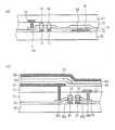
図3は、それぞれ図2のB−B線に沿った有機EL表示装置の一表示画素の断面図を示す。 FIG. 3 is a cross-sectional view of one display pixel of the organic EL display device along the line BB in FIG.
一表示画素は割り当てられたR、G、Bのいずれかを発光する有機EL素子160と、ゲート信号線51によってデータ信号を取り込む第1TFT30と、この第1TFT30を介してドレイン信号線52から供給されたデータ信号を保持する保持容量SCと、保持されたドレイン信号に応じて駆動電源線53を介して電流を有機EL素子160に供給する第2TFT40を備えている。なお、これらのうち、図2のA−A線に沿った第1TFT30及び保持容量SCの断面は上述の図8(a)と共通するため説明を省略する。また、図3において、第2TFT40は上述の図8(b)と共通する。 One display pixel is supplied from an
有機EL素子160は、第2TFT40のソース43sに接続された陽極161と、基板上において共通電極として形成された陰極166と、この両電極の間に有機化合物を配置した発光素子層165とが形成されて構成されている。発光素子層165は、少なくとも発光層を含み、単一層でも多層構造でも構成できるが、一例として、図示するように陽極161側から順にホール輸送層162、発光層163、電子輸送層164から構成される。 The
また、本実施の形態においては、図1に示すように基板上にマトリクス状に配置された複数の表示画素R,G,Bを発光してカラー表示を行うために、R用、G用、B用の有機EL素子160では、それぞれ異なる材料、特に発光機能を備える有機化合物として異なる材料を用いる。 In the present embodiment, as shown in FIG. 1, in order to perform color display by emitting light from a plurality of display pixels R, G, and B arranged in a matrix on a substrate, R, G, In the
例えば、R用有機EL素子160Rでは、陽極161としてITO、ホール輸送層16
2として、MTDATA(第1ホール輸送層)及びTPD(第2ホール輸送層)、発光層163としてはZnPrを2%ドープしたBeBq2、陰極166としてMgIn合金を用いる。For example, in the
As 2, MTDATA (first hole transport layer) and TPD (second hole transport layer), BeBq2 was 2% doped ZnPr as light-emitting
また、G用有機EL素子160Gでは、陽極161としてITO、ホール輸送層162として、MTDATA(第1ホール輸送層)及びTPD(第2ホール輸送層)、発光層163としてはBeBq2、陰極166としてMgIn合金を用いる。In the
更に、B用有機EL素子160Bでは、陽極161としてITO、ホール輸送層162として、MTDATA(第1ホール輸送層)及びTPD(第2ホール輸送層)、発光層163としては1AZM−Hex、陰極としてMgIn合金を用いる。 Further, in the
またB用有機EL素子160Bとしては、他にITO(陽極)/MTDATA(第1ホール輸送層)・TPD(第2ホール輸送層)/OXD−8(発光層)/MgIn(陰極)の組み合わせでも良い。In addition, the
なお、上述の各化合物の略称の正式名称は、以下の通りである。
ZnPr:5,10,15,20-tetraphenylporphyrinato zinc
MTDATA:4,4,4-tris(3-methylphenylphenyl amino)triphenylamine
TPD:N,N-diphenyl-N,N-di(3-methylphenyl)-1,1-biphenyl-4,4-diamine
BeBq2:bis(10-hydroxybenzo[h]quinolinato)beryllium
1AZM-Hex:(N,N-disalicylidene-1,6-hexanediaminato)zinc
OXD-8:3-bis[5-(p-dimethylaminophenyl)-1,3,4-oxadiazol-2-y l]benzene
また、R,G,B用有機EL素子160(160R、160G、160B)としてこのような材料を採用した場合、発光効率は素子160G>素子160R>素子160Bとなる。有機EL素子160において、発光輝度は電流(電流密度)に依存性を示す。従って、各表示画素に同等の電流を供給した場合に、各色が同等な輝度となるようにするためには、上述のように素子発光領域面積を領域1G<領域1R<領域1Bと設定すればよい。In addition, the formal name of the abbreviation of each compound described above is as follows.
ZnPr: 5,10,15,20-tetraphenylporphyrinato zinc
MTDATA: 4,4,4-tris (3-methylphenylphenyl amino) triphenylamine
TPD: N, N-diphenyl-N, N-di (3-methylphenyl) -1,1-biphenyl-4,4-diamine
BeBq2 : bis (10-hydroxybenzo [h] quinolinato) beryllium
1AZM-Hex: (N, N-disalicylidene-1,6-hexanediaminato) zinc
OXD-8: 3-bis [5- (p-dimethylaminophenyl) -1,3,4-oxadiazol-2-yl] benzene
Further, when such a material is adopted as the organic EL element 160 (160R, 160G, 160B) for R, G, B, the light emission efficiency is
次に、各表示画素における発光面積をR,G,Bで適切な異なった大きさにするための表示画素の形成方法について説明する。 Next, a description will be given of a method for forming a display pixel in order to make the light emitting area of each display pixel appropriately different in R, G, and B.
その方法としては、(i)有機EL素子の陽極161の面積をR,G,Bで変える、(ii)陽極161の面積は同一として、陽極形成後、発光素子の層形成前に形成される平坦化絶縁膜167により陽極161の端部を覆うことで、陽極と発光素子層との接触面積をR,G,Bで変えるという方法がある。 As the method, (i) the area of the
まず、陽極の面積を異ならせて表示画素を形成する上述の(i)の方法について、図4を参照して説明する。なお、図4はR,G,B各色の有機EL素子160の陽極161を形成するためのマスクを表している。 First, the above-described method (i) for forming display pixels with different anode areas will be described with reference to FIG. FIG. 4 shows a mask for forming the
マスク200Aは、図1に示すように発光領域面積を1G<1R<1Bとするためのマスクであり、目的とする陽極の大きさに応じた開口部201が形成されている。同図において最も大きい開口部は、発光効率がR,G,Bのうち最も低い青色の有機EL素子用陽極のための開口部201B、最も小さな開口部は、最も発光効率が高い緑色の有機EL素子用陽極のための開口部201Gである。また、開口部201Bと201Gの中間の大きさの開口部は、発光効率が緑色のEL素子より低く、青色のEL素子より高い赤色のEL素子用陽極のための開口部201Rである。 As shown in FIG. 1, the
以下に、図3(a)を参照して、(i)の方法について具体的に説明する。 Hereinafter, the method (i) will be described in detail with reference to FIG.
第2TFT40を形成し、このTFT40を覆うように層間絶縁膜15,TFT40のドレイン43dと接続された駆動電源線53、基板全面を覆う平坦化絶縁膜17を形成し、この平坦化絶縁膜17と層間絶縁膜15を貫通するようにTFT40のソース43s対応領域にコンタクトホールを形成し、このコンタクトホール及び平坦化絶縁膜17の全面を覆うように透明電極(陽極)材料であるITOをスパッタ法によって形成するまでの工程は、上述の図8(b)の構成と共通する。 A
ITOを形成した後、次にレジストを塗布し、図4に示すマスク200Aを用いて、露光、現像工程を施すことにより、マスク200Aの開口部201R,201G,201Bに対応した位置にのみレジストパターンが残り、このレジストパターンをエッチングマスクとして用いてITOを所定エッチャントにてエッチングして除去する。これにより、マスク200Aの開口部201R,201G,201Bに対応した大きさ及び位置にITOパターンが形成され、その結果、陽極161は、R,G,B毎に異なる大きさとなる。 After the ITO is formed, a resist is then applied, and exposure and development processes are performed using the
有機EL素子の陽極161を各表示画素領域に形成した後、R,G,B毎に異なる上述の有機化合物材料を用いてR,G,B用の発光素子層165をそれぞれ形成する。なお、有機EL素子において、発光素子層に用いられる材料は比較的高抵抗であり、発光領域は発光素子層のうち陽極と陰極との層間に挟まれた領域に限られる。 After the
従って、発光素子層は陽極形成領域と同一でも、また陽極形成領域より大きくても良いが、発光素子層上に形成される陰極と、陽極とが、陽極端部において短絡することを防止するため、本実施の形態においては、図3(a)に示すように、発光素子層はR、G、Bとも陽極を覆うようにこの陽極面積より大きく設定している。もちろん、陽極と陰極との間で短絡が起こらないように他の処置を施せば、必ずしも発光素子層165を陽極より大きくする必要はない。他の処置とは、例えば後述する図3(b)のように平坦化絶縁膜167を形成すること等である。 Therefore, the light emitting element layer may be the same as or larger than the anode forming area, but in order to prevent a short circuit between the cathode and the anode formed on the light emitting element layer at the anode end. In the present embodiment, as shown in FIG. 3A, the light emitting element layer is set larger than the anode area so as to cover the anodes of R, G, and B. Needless to say, the light emitting
ここで、上述のようにR用有機EL素子:ITO//MTDATA/TPD//BeBq2+ZnPr2%//MgIn、B用有機EL素子:ITO//MTDATA/TPD//BeBq2//MgIn、G用有機EL素子:ITO//MTDATA/TPD //1AZM-Hex//MgIn又はITO//MTDATA/TPD//OXD-8//MgInの構成を採用した場合、第1及び第2ホール輸送層から構成されるホール輸送層162としてR,G,Bで同一材料が用いられており、ホール輸送層162の形成に際してはR,G,Bの区別無く、対応する陽極上161及び平坦化絶縁膜17上の全面に形成すればよい。Here, as described above, the organic EL element for R: ITO // MTDATA / TPD // BeBq2 + ZnPr2% // MgIn, the organic EL element for B: ITO // MTDATA / TPD // BeBq2 // MgIn, Organic EL element for G: ITO // MTDATA / TPD // 1AZM-Hex // MgIn or ITO // MTDATA / TPD // OXD-8 // MgIn, the first and second hole transport layers The same material is used for R, G, and B as the
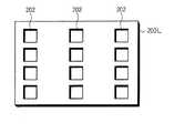
また、発光層163の形成にあたっては、上述のように本実施の形態においては、R,G,B用それぞれに異なる発光材料を用いており、各色用の発光層163の材料を変更して順に形成していく。各色の発光層163の形成に際しては、図5に示すようなマスク200Lを用いる。このマスク200Lはタングステン(W)等の金属であったり、あるいはシリコンなどが材料として用いられる。 In addition, in forming the
同図に示すように、マスク200Lは基板上に同一色の発光層を形成するための開口部202を有しており、それらの開口部202はマスク200Lの位置をシフトさせることにより図4に示したマスク200Aを用いて形成した各色の陽極と重畳するように設けられている。このとき、発光層の面積は陽極と同じ大きさであっても良く、陽極を覆って陽
極よりも大きい面積であっても良く、本実施の形態においては図3(a)に示すようにR,G,Bいずれの陽極より大きい大きさに設定している。As shown in the figure, the mask 200L has
例えば、青色を発光する発光層を蒸着する際には、蒸着前にマスク200Lを青色の発光層を形成予定領域にマスク200Lの開口部202が位置するように位置合わせして、ホール輸送層162上に密着させて配置する。その後、青色発光材料を蒸着することによって開口部202に応じた島状の青色発光層を形成する。 For example, when vapor-depositing a light-emitting layer that emits blue light, the
赤色発光層の蒸着にはマスク200Lを横方向にシフトさせ図5のマスク200Lの開口部202を赤色発光層の形成予定領域に位置合わせして用い、同様にして緑色発光層の蒸着に際してはマスク200Lの開口部202を緑色発光層の形成予定領域に位置合わせして用いる。このような手順により、R,G,Bで共に材料は異なるが同じ面積の発光層を順次島状にホール輸送層162上に形成する。こうして各色の発光層163を形成することができる。 For vapor deposition of the red light emitting layer, the mask 200L is shifted in the horizontal direction, and the
発光層163を形成後、電子輸送層164を必要とするEL素子160に対しては、発光層163上及びホール輸送層162上に電子輸送層164を蒸着形成することで電子輸送層164を形成する。 After the
以上のような手法により得られた発光素子層165を覆うようにマグネシウム・インジウム合金などをスパッタ法によって堆積し陰極166を形成する。これにより、R,G,B毎で陽極の面積が異なり素子発光面積がR,G,B毎に所望の面積となった有機EL素子を用いた表示装置が得られる。 A
次に、陽極の面積は同じで陽極と発光層との間に形成した平坦化絶縁膜で陽極と発光層との接触面積を異ならせる方法(上述の(ii))について説明する。 Next, a method of making the contact area between the anode and the light emitting layer different from each other with the planarizing insulating film formed between the anode and the light emitting layer with the same area (the above (ii)) will be described.
図3(b)に示すように、陽極161上に設ける発光素子層165の陽極161の段差による断線することを防止するためには、陽極161の周縁部を平坦化絶縁膜167で覆うことが好適である。このような構成の有機EL素子の場合、実質的に発光する領域、即ち発光面積は発光素子層165が陽極161と接触している面積であり、この平坦化絶縁膜167によって覆われた陽極161の周縁部は実質的に発光しない領域となる。 As shown in FIG. 3B, in order to prevent the light emitting
従って、平坦化絶縁膜167で覆う陽極161の周縁部の面積のみ各色で異ならせることにより、各色の表示画素の発光面積を異ならせることができる。 Therefore, by changing the area of the peripheral portion of the
このように各色の表示画素の発光面積を異ならせることによっても、EL素子の長寿命化が図れる。 Thus, the lifetime of the EL element can also be extended by changing the light emitting area of each color display pixel.
なお、本実施の形態においては、発光効率がG>R>Bの場合に、表示画素の発光面積をG<R<Bとし、各色でそれぞれ発光面積をこの順に異なるものとした場合を例にして説明したが、本発明はこれに限定するものはない。例えば、発光効率が同じくG>R>Bの場合において、発光面積はG≒R<Bとしても良いし、G<R≒Bとしても良い。 In the present embodiment, when the luminous efficiency is G> R> B, the case where the light emitting area of the display pixel is G <R <B and the light emitting area is different for each color in this order is taken as an example. However, the present invention is not limited to this. For example, when the light emission efficiency is G> R> B, the light emission area may be G≈R <B or G <R≈B.
また、陽極161の周縁部に平坦化絶縁膜167を配置したが、平坦化絶縁膜に限るものではなく、絶縁性を有するものであればよい。 Further, although the
以上のようにすることにより、電流量が大きいほど劣化が早まる傾向を示す有機EL素子において、低発光効率の表示画素のEL素子発光層に、他の色の発光層よりも大きい電流を流すことで各色が同様に明るく光るようにさせると低発光効率の素子が選択的に劣化
するといった不具合が発生することが防止でき、どの色の有機EL素子も同様の期間劣化を防ぐことが可能となり、その結果、表示装置全体としての寿命を長くできる。As described above, in an organic EL element that tends to be deteriorated as the amount of current increases, a current larger than that of the light emitting layers of other colors is caused to flow in the EL element light emitting layer of the display pixel having low light emission efficiency. If each color is made to shine brightly in the same manner, it is possible to prevent the occurrence of a problem that the elements with low light emission efficiency are selectively deteriorated, and it is possible to prevent the organic EL elements of any color from being deteriorated in the same period, As a result, the lifetime of the entire display device can be extended.
面積比の一例としては、次のようなものが挙げられる。 Examples of area ratios include the following.
例えば、発光する緑、赤、青の各色光の輝度を1:1:1とする場合、供給電流を一定とすると、発光効率の比が、10:3.8:1.8の場合である。各色とも輝度”1”成するために必要な各色の発光面積の比は、1/10:1/3.8:1/1.8=1:2.6:5.6である。 For example, when the luminance of each of the emitted green, red, and blue light is 1: 1: 1, and the supply current is constant, the luminous efficiency ratio is 10: 3.8: 1.8. . The ratio of the light emission areas of the respective colors required for achieving luminance “1” for each color is 1/10: 1 / 3.8: 1 / 1.8 = 1: 2.6: 5.6.
このような発光面積比にすることにより、発光効率が最も悪い色の青色だけに大きな電流を流すことなく、R,G,Bを同様な輝度で発光させることができるので発光層の寿命を長くすることが可能となる。 By setting such a light emitting area ratio, R, G, and B can emit light with the same luminance without flowing a large current only to the blue color having the worst light emitting efficiency, so that the life of the light emitting layer is extended. It becomes possible to do.
次に、面積比の他の例について説明する。この例は、発光効率の低い色の有機EL素子の劣化を防止すると共に、フルカラー表示におけるホワイトバランスの制御を考慮した場合の例である。 Next, another example of the area ratio will be described. This example is an example in which deterioration of the organic EL element having a low light emission efficiency is prevented and white balance control in full color display is taken into consideration.
自発光素子である有機EL素子を表示画素に用いてカラー表示を行う場合、各R,G,Bそれぞれの有機EL素子からの発光光を加算することにより白が表示される。 When color display is performed using an organic EL element, which is a self-luminous element, as a display pixel, white is displayed by adding light emitted from each of the R, G, and B organic EL elements.
目標として設定する白色を、NTSC方式の基準白色光源(C光源)の色度座標(x、y)=(0.31,0.32)とする場合に、このような白色の輝度100%を達成するためにR,G,Bに要求される輝度は、各有機EL素子の発するR,G,Bの各色の色度が、図6の上段に示すような座標で表される場合に、例えば、25%:46%:29%というように決まる。これは輝度比で示すと、R:G:B=0.54:1:0.63となる。 When the white color to be set as the target is the chromaticity coordinate (x, y) = (0.31, 0.32) of the NTSC standard white light source (C light source), such a white luminance of 100% is obtained. The luminance required for R, G, and B to achieve this is when the chromaticity of each color of R, G, and B emitted from each organic EL element is expressed by coordinates as shown in the upper part of FIG. For example, it is determined as 25%: 46%: 29%. In terms of luminance ratio, R: G: B = 0.54: 1: 0.63.
また、有機EL素子の各色における発光効率の比が、上述の例と同様にG,R,Bについて、10:3.8:1.8の場合、G,R,Bの輝度比G:R:B=1:0.54:0.63を達成するために必要な発光面積の比は、G:R:B=1/10:0.54/3.8:0.63/1.8=1:14.2:35ということになる。 Further, when the ratio of the luminous efficiency of each color of the organic EL element is 10: 3.8: 1.8 for G, R, and B as in the above example, the luminance ratio G: R of G, R, and B : B = 1: 0.54: 0.63 The ratio of the light emitting area required to achieve G: R: B = 1/10: 0.54 / 3.8: 0.63 / 1.8 = 1: 14.2: 35.
このように、R,G,Bの色度と目標白色の色度、そして各色の発光効率を考慮し、例えば発光領域の面積比が上述の値になるように、R,G,B用の発光面積を設定すれば、各表示画素の有機EL素子に同量の電流を供給した場合に、白の輝度100%を達成することが可能となる。 Thus, considering the chromaticity of R, G, and B, the chromaticity of the target white, and the luminous efficiency of each color, for example, for R, G, and B so that the area ratio of the light emitting region becomes the above value. If the light emitting area is set, white luminance of 100% can be achieved when the same amount of current is supplied to the organic EL element of each display pixel.
なお、目標とする白色の色度又は各色の色度が変わると、上述のように輝度比によって決まる各色の発光面積の順番も変わることになる。 Note that when the target white chromaticity or the chromaticity of each color changes, the order of the emission areas of the respective colors determined by the luminance ratio as described above also changes.
以上のように、このような方法により面積比を決定したEL表示装置では、各色の輝度バランスが発光面積で調整されているので、ホワイトバランスの制御が非常に容易であるとともに、白を表示するために特定の色のEL素子にのみ多く電流を流す必要が無くなり、表示装置全体としての寿命を向上することも可能となる。 As described above, in the EL display device in which the area ratio is determined by such a method, since the luminance balance of each color is adjusted by the light emission area, white balance control is very easy and white is displayed. Therefore, it is not necessary to supply a large amount of current only to the EL elements of a specific color, and the lifetime of the entire display device can be improved.
なお、使用する材料が異なれば有機EL素子の発するR,G,Bの光の色度座標値が異なるため、R,G,Bの輝度比もそれに応じて変わり、また発光効率も異なるため、発光面積比はこれに応じて決まり、上述の数値のものに限られない。 In addition, since the chromaticity coordinate value of the light of R, G, and B emitted from the organic EL element is different if the material used is different, the luminance ratio of R, G, and B is changed accordingly, and the luminous efficiency is also different. The light emission area ratio is determined accordingly, and is not limited to the above numerical values.
また、本発明ではR,G,Bの有機EL素子にそれぞれ同一電流を供給した場合に、常時白色100%が達成されるように素子の発光面積が設定されている構成に限るものではない。例えば、各表示画素を駆動する図示しないドライバ等を更に考慮した上で、装置全体としてホワイトバランスの制御が容易で、かつ発光効率の低い素子に選択的に負荷がかかることを防止できるように、R,G,Bの各有機EL素子の発光面積を設定しても良い。 The present invention is not limited to the configuration in which the light emitting area of the element is set so that 100% white is always achieved when the same current is supplied to the R, G, and B organic EL elements. For example, in consideration of a driver (not shown) that drives each display pixel, white balance can be easily controlled as a whole device, and an element having low luminous efficiency can be prevented from being selectively loaded. You may set the light emission area of each organic EL element of R, G, B.
更に上述の実施の形態においては、有機EL表示装置を例に挙げて説明したが、本発明はそれに限定されるものではなく、発光素子として有機EL素子に代えて、発光材料に向き発光材料が用いられた無機EL素子を用いた無機EL表示装置や、2つの電極の間に発光層として蛍光層を備える蛍光表示管(VFD:Vacuum Fluorescent Display)等においても有機EL表示装置と同様の効果が得られる。 Furthermore, in the above-described embodiment, the organic EL display device has been described as an example. However, the present invention is not limited thereto, and instead of the organic EL element as a light emitting element, a light emitting material is used as a light emitting material. Inorganic EL display devices using the used inorganic EL elements and fluorescent display tubes (VFD: Vacuum Fluorescent Display) having a fluorescent layer as a light emitting layer between two electrodes have the same effects as organic EL display devices. can get.
VFDは、図3で示したEL素子と同様に、絶縁性基板10上に形成したTFTを用いて駆動する。VFDは、図3において、陽極161の形成までの工程及び構造はEL素子と同じである。ただし、陽極161はAl等の金属から成っている。その上には蛍光物質を堆積し、その上方にはグリッド及び陰極(フィラメント)が配置されている。陽極及び陰極で囲まれる間隙は真空状態である。 The VFD is driven using a TFT formed on the insulating
フィラメントから発せられた熱電子がグリッドで整流化されて、陽極上の蛍光物質に衝突して発光する。こうして自ら光を発する。所定の色を発する蛍光物質を選択することにより所定の色を発することができる。また、発光面積は、上述のEL素子の場合と同様に決めればよい。即ち、蛍光物質の発光効率に応じて発光面積を決定すれば良い。 Thermoelectrons emitted from the filament are rectified by the grid and collide with the fluorescent material on the anode to emit light. In this way, it emits light itself. A predetermined color can be emitted by selecting a fluorescent material that emits a predetermined color. Further, the light emitting area may be determined in the same manner as in the case of the EL element described above. That is, the light emission area may be determined according to the light emission efficiency of the fluorescent material.
なお、本発明において、表示画素の発光面積とは、表示画素の発光素子が実際に発光する領域の面積である。 In the present invention, the light emitting area of the display pixel is an area of a region where the light emitting element of the display pixel actually emits light.
即ち、図3(b)に示すように、陽極の厚みによる段差に起因して発光層が段切れを起こして陰極と短絡してしまうことを防止するために設けた平坦化絶縁膜が、陽極の周辺部を覆っている場合には、陽極と発光素子層とが直接接することにより実質的に発光する領域の面積をいう。 That is, as shown in FIG. 3B, the planarization insulating film provided to prevent the light emitting layer from being stepped and short-circuited with the cathode due to a step due to the thickness of the anode is Is the area of a region that substantially emits light when the anode and the light emitting element layer are in direct contact with each other.
更に言い換えると、有機EL素子の発光素子層が、陽極又は陰極の少なくとも一方の電極と直接接触する面積のうち、小さい方の面積をいう。 Furthermore, in other words, the light emitting element layer of the organic EL element refers to the smaller area among the areas in direct contact with at least one of the anode and the cathode.
また、本実施の形態においては、各表示画素の数を4行X7列の場合について示したが、本発明はそれに限定されるものではなく、VGA(640X480)、SVGA(800X600)、XGA(1024X768)、SXGA(1280X1024)など、任意の表示画素数に適用可能である。 In this embodiment, the number of display pixels is 4 rows × 7 columns. However, the present invention is not limited to this, and VGA (640 × 480), SVGA (800 × 600), XGA (1024 × 768). ), SXGA (1280 × 1024), etc., and can be applied to an arbitrary number of display pixels.
また、各陽極の形状は「L」字の場合を示したが、本発明はこれに限定されるものではなく、長方形でも、正方形でも良く、形状は発光層の発光に支障のない形状であれば制限はない。 In addition, although the shape of each anode is shown as “L”, the present invention is not limited to this, and may be rectangular or square, and the shape may be a shape that does not hinder the light emission of the light emitting layer. There is no limit.
また、上述の実施の形態においては、各色の表示画素の配列がストライプ配列の場合について説明したが、本発明はそれに限定されるものではなく、デルタ配列、ダイアゴナル配列でも同様の効果が得られる。 In the above-described embodiment, the case where the arrangement of display pixels of each color is a stripe arrangement has been described. However, the present invention is not limited to this, and the same effect can be obtained by a delta arrangement or a diagonal arrangement.
更に、上述の実施の形態においては、ゲート電極が能動層の下層に配置されたいわゆるボトムゲート型TFTの場合を説明したが、本発明はそれに限定されるものではなく、ゲ
ート電極が能動層の上層にあるいわゆるトップゲート型TFTであっても同様の効果が得られる。Further, in the above-described embodiment, the case of the so-called bottom gate type TFT in which the gate electrode is disposed in the lower layer of the active layer has been described. However, the present invention is not limited to this, and the gate electrode is formed of the active layer. The same effect can be obtained even in a so-called top gate TFT in the upper layer.
1B 青色の表示画素の発光領域
1R 赤色の表示画素の発光領域
1G 緑色の表示画素の発光領域
30 第1のTFT
40 第2のTFT
51 ゲート信号線
52 ドレイン信号線
53 駆動電源線
54 保持容量電極線
100 EL表示装置
161 陽極
163 発光層
165 発光素子層
166 陰極
200A 陽極形成用マスク
200L 発光層形成用マスク
201R 陽極形成用マスクの開口部
201G 陽極形成用マスクの開口部
201B 陽極形成用マスクの開口部
202 発光層形成用マスクの開口部1B Blue display
40 Second TFT
51
Claims (9)
Translated fromJapanese各色の表示画素のうちいずれかの色の表示画素の発光面積と他の色の表示画素の発光面積とを、前記平坦化絶縁膜の開口部の大小によって異ならせているとともに、
前記ホール輸送層は前記開口部により露出した陽極上と前記平坦化絶縁膜上の全面を覆い、かつ、前記発光層の下側に設けられ、
前記発光層は前記ホール輸送層上であって前記陰極の下側に各色毎に島状に設けられるとともに、前記平坦化絶縁膜の開口部及び平坦部と重畳し、さらに、前記陰極は前記各表示画素を覆った共通電極であることを特徴とするカラー有機EL表示装置。Each display pixel includes an organic EL element having a hole transport layer and a light-emitting layer made of adifferent organic material foreach color between the anode and the cathode, covers an end of the anode, and has an opening corresponding to the anode. In a color organic EL display device having a planarized insulating film provided,
The emission area of the display pixel of any color and the emission area of the display pixel of the other color among the display pixels of each color are made different depending on the size of the opening of the planarization insulating film,
The hole transport layer covers the entire surface of the anode and the planarization insulating film exposed by the opening,and is provided below the light emitting layer,
The light emitting layer is provided on the hole transport layer onthe lower side of the cathode in an island shape for each color, and overlaps with the opening and the flat portion of the planarization insulating film. A color organic EL display device comprising a common electrode covering a display pixel.
Priority Applications (1)
| Application Number | Priority Date | Filing Date | Title |
|---|---|---|---|
| JP2005070782AJP4260126B2 (en) | 1999-02-26 | 2005-03-14 | Color organic EL display device |
Applications Claiming Priority (3)
| Application Number | Priority Date | Filing Date | Title |
|---|---|---|---|
| JP5074299 | 1999-02-26 | ||
| JP2000024648 | 2000-02-02 | ||
| JP2005070782AJP4260126B2 (en) | 1999-02-26 | 2005-03-14 | Color organic EL display device |
Related Parent Applications (1)
| Application Number | Title | Priority Date | Filing Date |
|---|---|---|---|
| JP2000047901ADivisionJP3670923B2 (en) | 1999-02-26 | 2000-02-24 | Color organic EL display device |
Related Child Applications (1)
| Application Number | Title | Priority Date | Filing Date |
|---|---|---|---|
| JP2008223922ADivisionJP4624452B2 (en) | 1999-02-26 | 2008-09-01 | Color organic EL display device |
Publications (2)
| Publication Number | Publication Date |
|---|---|
| JP2005166691A JP2005166691A (en) | 2005-06-23 |
| JP4260126B2true JP4260126B2 (en) | 2009-04-30 |
Family
ID=34743302
Family Applications (1)
| Application Number | Title | Priority Date | Filing Date |
|---|---|---|---|
| JP2005070782AExpired - LifetimeJP4260126B2 (en) | 1999-02-26 | 2005-03-14 | Color organic EL display device |
Country Status (1)
| Country | Link |
|---|---|
| JP (1) | JP4260126B2 (en) |
Families Citing this family (18)
| Publication number | Priority date | Publication date | Assignee | Title |
|---|---|---|---|---|
| JP4511119B2 (en)* | 2003-01-27 | 2010-07-28 | 三洋電機株式会社 | Electroluminescence display device and pattern layout method of electroluminescence display device |
| JP4715906B2 (en)* | 2008-11-13 | 2011-07-06 | ソニー株式会社 | Display device |
| JP5532481B2 (en) | 2009-05-13 | 2014-06-25 | Nltテクノロジー株式会社 | Color image display method, color filter substrate, color pixel array substrate, image display device, and electronic apparatus |
| KR101097341B1 (en) | 2010-03-09 | 2011-12-23 | 삼성모바일디스플레이주식회사 | Organic light emitting display apparatus |
| KR101614876B1 (en) | 2010-09-07 | 2016-04-25 | 삼성디스플레이 주식회사 | Organic light emitting diode display |
| US20120169682A1 (en)* | 2010-12-29 | 2012-07-05 | Delphi Technologies, Inc. | Organic light emitting diode display device having a two-sided substrate and method of forming the same |
| KR101399729B1 (en)* | 2011-01-20 | 2014-05-28 | 샤프 가부시키가이샤 | Substrate on which film is formed, and organic el display device |
| WO2013043197A1 (en)* | 2011-09-23 | 2013-03-28 | Universal Display Corporation | Digitized oled light source |
| TW201442226A (en) | 2013-03-21 | 2014-11-01 | Sony Corp | Display device and its manufacturing method, and electronic device |
| TWI604600B (en) | 2013-07-19 | 2017-11-01 | 群創光電股份有限公司 | Organic electroluminesence display (oled) |
| CN108573998B (en) | 2018-04-19 | 2021-01-26 | 京东方科技集团股份有限公司 | Display panel, manufacturing method, and display device |
| US20220173171A1 (en)* | 2019-04-08 | 2022-06-02 | Sharp Kabushiki Kaisha | Display device |
| JP7360272B2 (en)* | 2019-08-19 | 2023-10-12 | 株式会社ジャパンディスプレイ | display device |
| JP2021044223A (en)* | 2019-09-13 | 2021-03-18 | 株式会社ジャパンディスプレイ | Display device |
| CN113097417B (en)* | 2021-03-30 | 2023-04-18 | 云南创视界光电科技有限公司 | OLED display substrate and display device |
| WO2022249447A1 (en)* | 2021-05-28 | 2022-12-01 | シャープディスプレイテクノロジー株式会社 | Display device and method for manufacturing display device |
| CN114203929B (en)* | 2021-12-09 | 2023-09-05 | 武汉华星光电半导体显示技术有限公司 | Display panel and mobile terminal |
| WO2025013622A1 (en)* | 2023-07-12 | 2025-01-16 | ソニーセミコンダクタソリューションズ株式会社 | Display device and method for manufacturing display device |
- 2005
- 2005-03-14JPJP2005070782Apatent/JP4260126B2/ennot_activeExpired - Lifetime
Also Published As
| Publication number | Publication date |
|---|---|
| JP2005166691A (en) | 2005-06-23 |
Similar Documents
| Publication | Publication Date | Title |
|---|---|---|
| JP4624452B2 (en) | Color organic EL display device | |
| JP3670923B2 (en) | Color organic EL display device | |
| US7091936B1 (en) | Color display device | |
| JP4260126B2 (en) | Color organic EL display device | |
| JP4121514B2 (en) | ORGANIC LIGHT EMITTING ELEMENT AND DISPLAY DEVICE INCLUDING THE SAME | |
| US8669701B2 (en) | Organic EL element array | |
| US10998395B2 (en) | Organic light-emitting display device | |
| TWI500144B (en) | Organic light emitting display device and method of manufacturing same | |
| JP4365364B2 (en) | Organic electroluminescent device and manufacturing method thereof | |
| KR102578834B1 (en) | Organic Light Emitting Display Device | |
| JP4574342B2 (en) | Organic electroluminescent device and manufacturing method thereof | |
| US20080001544A1 (en) | Organic Light-Emitting Display Device | |
| US20110315970A1 (en) | Organic el display device and method of manufacturing the same | |
| JP2000227771A (en) | Color el display device | |
| KR20060023180A (en) | Organic EL panel and its manufacturing method | |
| JP3481231B2 (en) | Organic electroluminescent display device and method of manufacturing the same | |
| JP4596582B2 (en) | Display device | |
| KR101978779B1 (en) | Organic Light Emitting Diode Display And Method For Manufacturing The Same | |
| KR100590255B1 (en) | Organic electroluminescent display and manufacturing method thereof | |
| US6686215B2 (en) | Method of producing an electroluminescence display device | |
| JP2008153237A (en) | ORGANIC LIGHT EMITTING ELEMENT AND DISPLAY DEVICE INCLUDING THE SAME | |
| KR101744874B1 (en) | Organic light emitting diodes | |
| JP2021057227A (en) | Self-luminous panel and manufacturing method of the same | |
| KR100530799B1 (en) | Hybrid Structure Organic Electroluminescent Device and method for fabricating the same | |
| KR20100020570A (en) | Luminescence dispaly panel and fabricating method of the same |
Legal Events
| Date | Code | Title | Description |
|---|---|---|---|
| A621 | Written request for application examination | Free format text:JAPANESE INTERMEDIATE CODE: A621 Effective date:20050314 | |
| RD01 | Notification of change of attorney | Free format text:JAPANESE INTERMEDIATE CODE: A7421 Effective date:20051227 | |
| A131 | Notification of reasons for refusal | Free format text:JAPANESE INTERMEDIATE CODE: A131 Effective date:20080304 | |
| A521 | Request for written amendment filed | Free format text:JAPANESE INTERMEDIATE CODE: A523 Effective date:20080410 | |
| A131 | Notification of reasons for refusal | Free format text:JAPANESE INTERMEDIATE CODE: A131 Effective date:20080708 | |
| A521 | Request for written amendment filed | Free format text:JAPANESE INTERMEDIATE CODE: A523 Effective date:20080902 | |
| TRDD | Decision of grant or rejection written | ||
| A01 | Written decision to grant a patent or to grant a registration (utility model) | Free format text:JAPANESE INTERMEDIATE CODE: A01 Effective date:20090106 | |
| A01 | Written decision to grant a patent or to grant a registration (utility model) | Free format text:JAPANESE INTERMEDIATE CODE: A01 | |
| A61 | First payment of annual fees (during grant procedure) | Free format text:JAPANESE INTERMEDIATE CODE: A61 Effective date:20090203 | |
| FPAY | Renewal fee payment (event date is renewal date of database) | Free format text:PAYMENT UNTIL: 20120220 Year of fee payment:3 | |
| R151 | Written notification of patent or utility model registration | Ref document number:4260126 Country of ref document:JP Free format text:JAPANESE INTERMEDIATE CODE: R151 | |
| FPAY | Renewal fee payment (event date is renewal date of database) | Free format text:PAYMENT UNTIL: 20120220 Year of fee payment:3 | |
| FPAY | Renewal fee payment (event date is renewal date of database) | Free format text:PAYMENT UNTIL: 20120220 Year of fee payment:3 | |
| FPAY | Renewal fee payment (event date is renewal date of database) | Free format text:PAYMENT UNTIL: 20130220 Year of fee payment:4 | |
| FPAY | Renewal fee payment (event date is renewal date of database) | Free format text:PAYMENT UNTIL: 20130220 Year of fee payment:4 | |
| FPAY | Renewal fee payment (event date is renewal date of database) | Free format text:PAYMENT UNTIL: 20140220 Year of fee payment:5 | |
| R250 | Receipt of annual fees | Free format text:JAPANESE INTERMEDIATE CODE: R250 | |
| EXPY | Cancellation because of completion of term |