JP4258518B2 - Film forming method, film forming apparatus, and storage medium - Google Patents
Film forming method, film forming apparatus, and storage mediumDownload PDFInfo
- Publication number
- JP4258518B2 JP4258518B2JP2006004191AJP2006004191AJP4258518B2JP 4258518 B2JP4258518 B2JP 4258518B2JP 2006004191 AJP2006004191 AJP 2006004191AJP 2006004191 AJP2006004191 AJP 2006004191AJP 4258518 B2JP4258518 B2JP 4258518B2
- Authority
- JP
- Japan
- Prior art keywords
- gas
- film
- film forming
- supply
- silane
- Prior art date
- Legal status (The legal status is an assumption and is not a legal conclusion. Google has not performed a legal analysis and makes no representation as to the accuracy of the status listed.)
- Active
Links
Images


Classifications
- H—ELECTRICITY
- H01—ELECTRIC ELEMENTS
- H01L—SEMICONDUCTOR DEVICES NOT COVERED BY CLASS H10
- H01L21/00—Processes or apparatus adapted for the manufacture or treatment of semiconductor or solid state devices or of parts thereof
- H01L21/02—Manufacture or treatment of semiconductor devices or of parts thereof
- H01L21/02104—Forming layers
- H01L21/02107—Forming insulating materials on a substrate
- H01L21/02225—Forming insulating materials on a substrate characterised by the process for the formation of the insulating layer
- H01L21/0226—Forming insulating materials on a substrate characterised by the process for the formation of the insulating layer formation by a deposition process
- H01L21/02263—Forming insulating materials on a substrate characterised by the process for the formation of the insulating layer formation by a deposition process deposition from the gas or vapour phase
- H01L21/02271—Forming insulating materials on a substrate characterised by the process for the formation of the insulating layer formation by a deposition process deposition from the gas or vapour phase deposition by decomposition or reaction of gaseous or vapour phase compounds, i.e. chemical vapour deposition
- C—CHEMISTRY; METALLURGY
- C23—COATING METALLIC MATERIAL; COATING MATERIAL WITH METALLIC MATERIAL; CHEMICAL SURFACE TREATMENT; DIFFUSION TREATMENT OF METALLIC MATERIAL; COATING BY VACUUM EVAPORATION, BY SPUTTERING, BY ION IMPLANTATION OR BY CHEMICAL VAPOUR DEPOSITION, IN GENERAL; INHIBITING CORROSION OF METALLIC MATERIAL OR INCRUSTATION IN GENERAL
- C23C—COATING METALLIC MATERIAL; COATING MATERIAL WITH METALLIC MATERIAL; SURFACE TREATMENT OF METALLIC MATERIAL BY DIFFUSION INTO THE SURFACE, BY CHEMICAL CONVERSION OR SUBSTITUTION; COATING BY VACUUM EVAPORATION, BY SPUTTERING, BY ION IMPLANTATION OR BY CHEMICAL VAPOUR DEPOSITION, IN GENERAL
- C23C16/00—Chemical coating by decomposition of gaseous compounds, without leaving reaction products of surface material in the coating, i.e. chemical vapour deposition [CVD] processes
- C23C16/22—Chemical coating by decomposition of gaseous compounds, without leaving reaction products of surface material in the coating, i.e. chemical vapour deposition [CVD] processes characterised by the deposition of inorganic material, other than metallic material
- C23C16/30—Deposition of compounds, mixtures or solid solutions, e.g. borides, carbides, nitrides
- C23C16/36—Carbonitrides
- C—CHEMISTRY; METALLURGY
- C23—COATING METALLIC MATERIAL; COATING MATERIAL WITH METALLIC MATERIAL; CHEMICAL SURFACE TREATMENT; DIFFUSION TREATMENT OF METALLIC MATERIAL; COATING BY VACUUM EVAPORATION, BY SPUTTERING, BY ION IMPLANTATION OR BY CHEMICAL VAPOUR DEPOSITION, IN GENERAL; INHIBITING CORROSION OF METALLIC MATERIAL OR INCRUSTATION IN GENERAL
- C23C—COATING METALLIC MATERIAL; COATING MATERIAL WITH METALLIC MATERIAL; SURFACE TREATMENT OF METALLIC MATERIAL BY DIFFUSION INTO THE SURFACE, BY CHEMICAL CONVERSION OR SUBSTITUTION; COATING BY VACUUM EVAPORATION, BY SPUTTERING, BY ION IMPLANTATION OR BY CHEMICAL VAPOUR DEPOSITION, IN GENERAL
- C23C16/00—Chemical coating by decomposition of gaseous compounds, without leaving reaction products of surface material in the coating, i.e. chemical vapour deposition [CVD] processes
- C23C16/44—Chemical coating by decomposition of gaseous compounds, without leaving reaction products of surface material in the coating, i.e. chemical vapour deposition [CVD] processes characterised by the method of coating
- C23C16/455—Chemical coating by decomposition of gaseous compounds, without leaving reaction products of surface material in the coating, i.e. chemical vapour deposition [CVD] processes characterised by the method of coating characterised by the method used for introducing gases into reaction chamber or for modifying gas flows in reaction chamber
- C23C16/45523—Pulsed gas flow or change of composition over time
- C—CHEMISTRY; METALLURGY
- C23—COATING METALLIC MATERIAL; COATING MATERIAL WITH METALLIC MATERIAL; CHEMICAL SURFACE TREATMENT; DIFFUSION TREATMENT OF METALLIC MATERIAL; COATING BY VACUUM EVAPORATION, BY SPUTTERING, BY ION IMPLANTATION OR BY CHEMICAL VAPOUR DEPOSITION, IN GENERAL; INHIBITING CORROSION OF METALLIC MATERIAL OR INCRUSTATION IN GENERAL
- C23C—COATING METALLIC MATERIAL; COATING MATERIAL WITH METALLIC MATERIAL; SURFACE TREATMENT OF METALLIC MATERIAL BY DIFFUSION INTO THE SURFACE, BY CHEMICAL CONVERSION OR SUBSTITUTION; COATING BY VACUUM EVAPORATION, BY SPUTTERING, BY ION IMPLANTATION OR BY CHEMICAL VAPOUR DEPOSITION, IN GENERAL
- C23C16/00—Chemical coating by decomposition of gaseous compounds, without leaving reaction products of surface material in the coating, i.e. chemical vapour deposition [CVD] processes
- C23C16/44—Chemical coating by decomposition of gaseous compounds, without leaving reaction products of surface material in the coating, i.e. chemical vapour deposition [CVD] processes characterised by the method of coating
- C23C16/455—Chemical coating by decomposition of gaseous compounds, without leaving reaction products of surface material in the coating, i.e. chemical vapour deposition [CVD] processes characterised by the method of coating characterised by the method used for introducing gases into reaction chamber or for modifying gas flows in reaction chamber
- C23C16/45563—Gas nozzles
- C23C16/45578—Elongated nozzles, tubes with holes
- C—CHEMISTRY; METALLURGY
- C23—COATING METALLIC MATERIAL; COATING MATERIAL WITH METALLIC MATERIAL; CHEMICAL SURFACE TREATMENT; DIFFUSION TREATMENT OF METALLIC MATERIAL; COATING BY VACUUM EVAPORATION, BY SPUTTERING, BY ION IMPLANTATION OR BY CHEMICAL VAPOUR DEPOSITION, IN GENERAL; INHIBITING CORROSION OF METALLIC MATERIAL OR INCRUSTATION IN GENERAL
- C23C—COATING METALLIC MATERIAL; COATING MATERIAL WITH METALLIC MATERIAL; SURFACE TREATMENT OF METALLIC MATERIAL BY DIFFUSION INTO THE SURFACE, BY CHEMICAL CONVERSION OR SUBSTITUTION; COATING BY VACUUM EVAPORATION, BY SPUTTERING, BY ION IMPLANTATION OR BY CHEMICAL VAPOUR DEPOSITION, IN GENERAL
- C23C16/00—Chemical coating by decomposition of gaseous compounds, without leaving reaction products of surface material in the coating, i.e. chemical vapour deposition [CVD] processes
- C23C16/44—Chemical coating by decomposition of gaseous compounds, without leaving reaction products of surface material in the coating, i.e. chemical vapour deposition [CVD] processes characterised by the method of coating
- C23C16/50—Chemical coating by decomposition of gaseous compounds, without leaving reaction products of surface material in the coating, i.e. chemical vapour deposition [CVD] processes characterised by the method of coating using electric discharges
- C23C16/515—Chemical coating by decomposition of gaseous compounds, without leaving reaction products of surface material in the coating, i.e. chemical vapour deposition [CVD] processes characterised by the method of coating using electric discharges using pulsed discharges
- H—ELECTRICITY
- H01—ELECTRIC ELEMENTS
- H01L—SEMICONDUCTOR DEVICES NOT COVERED BY CLASS H10
- H01L21/00—Processes or apparatus adapted for the manufacture or treatment of semiconductor or solid state devices or of parts thereof
- H01L21/70—Manufacture or treatment of devices consisting of a plurality of solid state components formed in or on a common substrate or of parts thereof; Manufacture of integrated circuit devices or of parts thereof
- H01L21/71—Manufacture of specific parts of devices defined in group H01L21/70
- H01L21/768—Applying interconnections to be used for carrying current between separate components within a device comprising conductors and dielectrics
- H01L21/76801—Applying interconnections to be used for carrying current between separate components within a device comprising conductors and dielectrics characterised by the formation and the after-treatment of the dielectrics, e.g. smoothing
- H01L21/76829—Applying interconnections to be used for carrying current between separate components within a device comprising conductors and dielectrics characterised by the formation and the after-treatment of the dielectrics, e.g. smoothing characterised by the formation of thin functional dielectric layers, e.g. dielectric etch-stop, barrier, capping or liner layers
- H—ELECTRICITY
- H01—ELECTRIC ELEMENTS
- H01L—SEMICONDUCTOR DEVICES NOT COVERED BY CLASS H10
- H01L21/00—Processes or apparatus adapted for the manufacture or treatment of semiconductor or solid state devices or of parts thereof
- H01L21/02—Manufacture or treatment of semiconductor devices or of parts thereof
- H01L21/02104—Forming layers
- H01L21/02107—Forming insulating materials on a substrate
- H01L21/02109—Forming insulating materials on a substrate characterised by the type of layer, e.g. type of material, porous/non-porous, pre-cursors, mixtures or laminates
- H01L21/02112—Forming insulating materials on a substrate characterised by the type of layer, e.g. type of material, porous/non-porous, pre-cursors, mixtures or laminates characterised by the material of the layer
- H01L21/02123—Forming insulating materials on a substrate characterised by the type of layer, e.g. type of material, porous/non-porous, pre-cursors, mixtures or laminates characterised by the material of the layer the material containing silicon
- H01L21/02126—Forming insulating materials on a substrate characterised by the type of layer, e.g. type of material, porous/non-porous, pre-cursors, mixtures or laminates characterised by the material of the layer the material containing silicon the material containing Si, O, and at least one of H, N, C, F, or other non-metal elements, e.g. SiOC, SiOC:H or SiONC
- H—ELECTRICITY
- H01—ELECTRIC ELEMENTS
- H01L—SEMICONDUCTOR DEVICES NOT COVERED BY CLASS H10
- H01L21/00—Processes or apparatus adapted for the manufacture or treatment of semiconductor or solid state devices or of parts thereof
- H01L21/02—Manufacture or treatment of semiconductor devices or of parts thereof
- H01L21/02104—Forming layers
- H01L21/02107—Forming insulating materials on a substrate
- H01L21/02109—Forming insulating materials on a substrate characterised by the type of layer, e.g. type of material, porous/non-porous, pre-cursors, mixtures or laminates
- H01L21/02205—Forming insulating materials on a substrate characterised by the type of layer, e.g. type of material, porous/non-porous, pre-cursors, mixtures or laminates the layer being characterised by the precursor material for deposition
- H01L21/02208—Forming insulating materials on a substrate characterised by the type of layer, e.g. type of material, porous/non-porous, pre-cursors, mixtures or laminates the layer being characterised by the precursor material for deposition the precursor containing a compound comprising Si
- H01L21/02211—Forming insulating materials on a substrate characterised by the type of layer, e.g. type of material, porous/non-porous, pre-cursors, mixtures or laminates the layer being characterised by the precursor material for deposition the precursor containing a compound comprising Si the compound being a silane, e.g. disilane, methylsilane or chlorosilane
- H—ELECTRICITY
- H01—ELECTRIC ELEMENTS
- H01L—SEMICONDUCTOR DEVICES NOT COVERED BY CLASS H10
- H01L21/00—Processes or apparatus adapted for the manufacture or treatment of semiconductor or solid state devices or of parts thereof
- H01L21/02—Manufacture or treatment of semiconductor devices or of parts thereof
- H01L21/02104—Forming layers
- H01L21/02107—Forming insulating materials on a substrate
- H01L21/02225—Forming insulating materials on a substrate characterised by the process for the formation of the insulating layer
- H01L21/0226—Forming insulating materials on a substrate characterised by the process for the formation of the insulating layer formation by a deposition process
- H01L21/02263—Forming insulating materials on a substrate characterised by the process for the formation of the insulating layer formation by a deposition process deposition from the gas or vapour phase
- H01L21/02271—Forming insulating materials on a substrate characterised by the process for the formation of the insulating layer formation by a deposition process deposition from the gas or vapour phase deposition by decomposition or reaction of gaseous or vapour phase compounds, i.e. chemical vapour deposition
- H01L21/0228—Forming insulating materials on a substrate characterised by the process for the formation of the insulating layer formation by a deposition process deposition from the gas or vapour phase deposition by decomposition or reaction of gaseous or vapour phase compounds, i.e. chemical vapour deposition deposition by cyclic CVD, e.g. ALD, ALE, pulsed CVD
Landscapes
- Chemical & Material Sciences (AREA)
- Engineering & Computer Science (AREA)
- Chemical Kinetics & Catalysis (AREA)
- General Chemical & Material Sciences (AREA)
- Organic Chemistry (AREA)
- Metallurgy (AREA)
- Mechanical Engineering (AREA)
- Materials Engineering (AREA)
- Physics & Mathematics (AREA)
- Condensed Matter Physics & Semiconductors (AREA)
- Power Engineering (AREA)
- Microelectronics & Electronic Packaging (AREA)
- Computer Hardware Design (AREA)
- Manufacturing & Machinery (AREA)
- General Physics & Mathematics (AREA)
- Plasma & Fusion (AREA)
- Inorganic Chemistry (AREA)
- Chemical Vapour Deposition (AREA)
- Formation Of Insulating Films (AREA)
Description
Translated fromJapanese本発明は、半導体ウエハ等の被処理体に薄膜を形成する成膜方法、成膜装置及びこの成膜装置をコンピュータ制御するプログラムを記憶する記憶媒体に関する。 The present invention relates to a film forming method for forming a thin film on an object to be processed such as a semiconductor wafer, a film forming apparatus, and a storage medium for storing a program for controlling the film forming apparatus by a computer.
一般に、半導体集積回路を製造するためにはシリコン基板等よりなる半導体ウエハに対して、成膜処理、エッチング処理、酸化処理、拡散処理、改質処理、自然酸化膜の除去処理等の各種の処理が行なわれる。これらの処理を特許文献1等に開示されている縦型の、いわゆるバッチ式の熱処理装置にて行う場合には、まず、半導体ウエハを複数枚、例えば25枚程度収容できるカセットから、半導体ウエハを縦型のウエハボートへ移載してこれに多段に支持させる。このウエハボートは、例えばウエハサイズにもよるが30〜150枚程度のウエハを載置できる。このウエハボートは、排気可能な処理容器内にその下方より搬入(ロード)された後、処理容器内が気密に維持される。そして、処理ガスの流量、プロセス圧力、プロセス温度等の各種のプロセス条件を制御しつつ所定の熱処理が施される。 Generally, in order to manufacture a semiconductor integrated circuit, various processes such as a film formation process, an etching process, an oxidation process, a diffusion process, a modification process, and a natural oxide film removal process are performed on a semiconductor wafer made of a silicon substrate or the like Is done. When these processes are performed in a so-called batch-type heat treatment apparatus disclosed in
ここで上記半導体集積回路の特性を向上させる要因の1つとして、集積回路中の絶縁膜の特性を向上させることは重要である。上記集積回路中の絶縁膜としては、一般的にはSiO2 、PSG(Phospho Silicate Glass)、P(プラズマ)−SiO、P(プラズマ)−SiN、SOG(Spin On Glass)、Si3 N4 (シリコン窒化膜)等が用いられる。そして、特にシリコン窒化膜は、絶縁特性がシリコン酸化膜より比較的良好なこと、及びエッチングストッパ膜や層間絶縁膜としても十分に機能することから多用される傾向にある。また同様な理由でボロン窒化膜も用いられる傾向にある。Here, as one of the factors for improving the characteristics of the semiconductor integrated circuit, it is important to improve the characteristics of the insulating film in the integrated circuit. As the insulating film in the integrated circuit, generally, SiO2 , PSG (Phospho Silicate Glass), P (plasma) -SiO, P (plasma) -SiN, SOG (Spin On Glass), Si3 N4 ( Silicon nitride film) or the like is used. In particular, the silicon nitride film tends to be frequently used because its insulating characteristics are relatively better than that of the silicon oxide film and it functions sufficiently as an etching stopper film and an interlayer insulating film. For the same reason, boron nitride films tend to be used.
半導体ウエハの表面に上述したようなシリコン窒化膜を形成するには、成膜ガスとしてモノシラン(SiH4 )やジクロルシラン(SiH2 Cl2 )やヘキサクロロジシラン(Si2 Cl6 )、ビス ターシャル ブチルアミノシラン(BTBAS)等のシラン系ガスを用いて熱CVD(Chemical Vapor Deposition)により成膜する方法が知られている。具体的には、シリコン窒化膜を堆積する場合には、SiH2 Cl2 +NH3 (特許文献1参照)或いはSi2 Cl6 +NH3 等のガスの組み合わせで熱CVDによりシリコン窒化膜を形成している。
そして、上記絶縁膜の誘電率を小さくするためにシリコン窒化膜に不純物として例えばボロン(B)を添加して絶縁膜を形成するようにした提案もなされている(特許文献2)。In order to form a silicon nitride film as described above on the surface of a semiconductor wafer, monosilane (SiH4 ), dichlorosilane (SiH2 Cl2 ), hexachlorodisilane (Si2 Cl6 ), bis-tertiary butylaminosilane ( A method of forming a film by thermal CVD (Chemical Vapor Deposition) using a silane-based gas such as BTBAS is known. Specifically, when depositing a silicon nitride film, the silicon nitride film is formed by thermal CVD using a combination of gases such as SiH2 Cl2 + NH3 (see Patent Document 1) or Si2 Cl6 + NH3. Yes.
In order to reduce the dielectric constant of the insulating film, a proposal has been made to form an insulating film by adding, for example, boron (B) as an impurity to the silicon nitride film (Patent Document 2).
ところで、最近にあっては半導体集積回路の更なる高集積化及び高微細化の要求が強くなされており、回路素子の特性の向上を目的として半導体集積回路の製造工程における熱履歴も低減化することが望まれている。このような状況下において、縦型の、いわゆるバッチ式の縦型の処理装置においても、ウエハをそれ程の高温に晒さなくても目的とする処理が可能なことから、原料ガス等を間欠的に供給しながら原子レベルで1層〜数層ずつ、或いは分子レベルで1層〜数層ずつ繰り返し成膜する方法が知られている(特許文献3、4等)。このような成膜方法は一般的にはALD(Atomic Layer Deposition)と称されている。 Recently, there is a strong demand for further integration and miniaturization of semiconductor integrated circuits, and the thermal history in the manufacturing process of semiconductor integrated circuits is also reduced for the purpose of improving the characteristics of circuit elements. It is hoped that. Under such circumstances, even in a vertical type, so-called batch type vertical processing apparatus, the target processing is possible without exposing the wafer to such a high temperature. There is known a method of repeatedly forming one to several layers at the atomic level or one to several layers at the molecular level while supplying (Patent Documents 3, 4, etc.). Such a film forming method is generally referred to as ALD (Atomic Layer Deposition).
ここで従来の成膜方法としては、シラン系ガスであるジクロロシラン(以下、「DCS」とも称す)と窒化ガスであるNH3 ガスとを用いてシリコン窒化膜(SiN)を形成している。具体的には、処理容器内に、DCSとNH3 ガスとを交互に間欠的に供給し、NH3 ガスを供給する時にRF(高周波)を印加してプラズマを立て、窒化反応を促進するようにしている。この場合、DCSを処理容器内へ供給することにより、ウエハ表面上にDCSが分子レベルで一層、或いは複数層吸着し、そして余分なDCSを不活性ガスパージ、或いは真空引きで排除した後、NH3 を供給してプラズマを立てることによって低温での窒化を促進して窒化膜を形成し、この一連の工程を繰り返し行っている。Here, as a conventional film forming method, a silicon nitride film (SiN) is formed using dichlorosilane (hereinafter also referred to as “DCS”) which is a silane-based gas and NH3 gas which is a nitriding gas. Specifically, DCS and NH3 gas are alternately and intermittently supplied into the processing vessel, and when NH3 gas is supplied, RF (radio frequency) is applied to generate plasma to promote the nitriding reaction. I have to. In this case, by supplying DCS into the processing vessel, DCS is adsorbed on the wafer surface in one or more layers at the molecular level, and excess DCS is removed by inert gas purging or evacuation, and then NH3 The plasma is generated to promote nitridation at a low temperature to form a nitride film, and this series of steps is repeated.
ところで、上述したような絶縁膜を形成した後に、この上に別の薄膜を形成する場合には、上記絶縁膜の表面が有機物やパーティクル等の汚染物が付着している可能性があるので、この汚染物を除去する目的で、上記半導体ウエハを希フッ酸等のクリーニング液に浸漬させて上記絶縁膜の表面をエッチングすることによりこの表面を非常に薄く削り取り、これにより上記汚染物を除去するクリーニング処理が行われる場合がある。
しかしながら、この場合、上記絶縁膜を例えば760℃程度の高温の熱CVDで成膜した場合には、このような高温の熱CVDで形成した絶縁膜のクリーニング時のエッチングレートはかなり小さいので、クリーニング時にこの絶縁膜が過度に削り取られることがなく、膜厚の制御性が良い状態でクリーニング処理を行うことができるが、下地層に耐熱性の低い薄膜が形成されている場合には、高温の熱CVD処理を採用できない。By the way, after forming the insulating film as described above, when another thin film is formed thereon, there is a possibility that contaminants such as organic substances and particles adhere to the surface of the insulating film. For the purpose of removing this contaminant, the surface of the insulating film is etched very thinly by immersing the semiconductor wafer in a cleaning solution such as dilute hydrofluoric acid, thereby removing the contaminant. A cleaning process may be performed.
However, in this case, when the insulating film is formed by high-temperature thermal CVD of about 760 ° C., for example, the etching rate at the time of cleaning of the insulating film formed by such high-temperature thermal CVD is considerably small. Sometimes this insulating film is not excessively scraped off, and the cleaning process can be performed with good controllability of the film thickness, but if a thin film with low heat resistance is formed on the underlayer, Thermal CVD process cannot be adopted.
これに対して、上記絶縁膜を例えば400℃程度の低い温度でALD成膜した場合には、このような低温で形成した絶縁膜のクリーニング時のエッチングレートはかなり大きいので、クリーニング時にこの絶縁膜が過度に削り取られる場合が発生し、クリーニング処理時の膜厚の制御性が劣ってしまう、といった問題があった。またこのシリコン窒化膜は前述したようにエッチングストッパ膜や層間絶縁膜等の絶縁膜として使用する場合もあるが、この場合にはエッチングレートを十分に小さくする必要があり、従来の成膜方法では、この要請に十分に応えることはできなかった。
本発明は、以上のような問題点に着目し、これを有効に解決すべく創案されたものである。本発明の目的は、比較的低温で成膜してもクリーニング時のエッチングレートを比較的小さくでき、もってクリーニング時の膜厚の制御性を向上させることができ、且つエッチングストッパ膜や層間絶縁膜等の絶縁膜として十分機能する絶縁膜を形成することができる成膜方法、成膜装置及び記憶媒体を提供することにある。尚、本発明は、本出願人が先に出願した特願2002−381826(特開2003−282566号公報)に開示した発明の改良発明である。On the other hand, when the ALD film is formed at a temperature as low as about 400 ° C., for example, the etching rate for cleaning the insulating film formed at such a low temperature is considerably high. There is a problem that the film thickness is excessively scraped off and the controllability of the film thickness during the cleaning process is poor. In addition, as described above, this silicon nitride film may be used as an insulating film such as an etching stopper film or an interlayer insulating film. In this case, it is necessary to sufficiently reduce the etching rate. This request was not fully met.
The present invention has been devised to pay attention to the above problems and to effectively solve them. It is an object of the present invention to reduce the etching rate during cleaning even if the film is formed at a relatively low temperature, thereby improving the controllability of the film thickness during cleaning, and to provide an etching stopper film and an interlayer insulating film. It is an object of the present invention to provide a film formation method, a film formation apparatus, and a storage medium that can form an insulating film that sufficiently functions as an insulating film. The present invention is an improved invention of the invention disclosed in Japanese Patent Application No. 2002-38826 (Japanese Patent Laid-Open No. 2003-282666) filed earlier by the present applicant.
請求項1に係る発明は、複数枚の被処理体が収容されて真空引き可能になされた処理容器内に、シラン系ガスと窒化ガスとボロン含有ガスと炭化水素ガスとを供給して前記被処理体の表面にSiBCN薄膜を形成する成膜方法において、前記シラン系ガスとボロン含有ガスと炭化水素ガスの3種類のガスの同時供給と前記窒化ガスの供給とを間欠的に且つ交互に行うようにしたことを特徴とする成膜方法である。
このように、上記シラン系ガスとボロン含有ガスと炭化水素ガスの3種類のガスの同時供給と前記窒化ガスの供給とを間欠的に且つ交互に行うようにしてSiBCN膜(シリコン・ボロン・カーボン窒化膜)を形成するようにしたので、比較的低温で成膜してもクリーニング時のエッチングレートを比較的小さくでき、もってクリーニング時の膜厚の制御性を向上させることができ、且つエッチングストッパ膜や層間絶縁膜等の絶縁膜として十分機能する絶縁膜を形成することができる。According to the first aspect of the present invention, a silane-based gas, a nitriding gas, a boron-containing gas, and a hydrocarbon gas are supplied into a processing container in which a plurality of objects to be processed are accommodated so as to be evacuated. In the film forming method for forming a SiBCN thin film on the surface of the treatment body, the simultaneous supply of the three types of gas, the silane-based gas, the boron-containing gas, and the hydrocarbon gas, and the supply of the nitriding gas are performed intermittently and alternately. The film forming method is characterized by the above.
In this way, the SiBCN film (silicon, boron, carbon) is supplied intermittently and alternately with the simultaneous supply of the three gases, the silane-based gas, the boron-containing gas, and the hydrocarbon gas, and the supply of the nitriding gas. Nitride film), the etching rate during cleaning can be made relatively small even when the film is formed at a relatively low temperature, the controllability of the film thickness during cleaning can be improved, and the etching stopper. An insulating film which functions sufficiently as an insulating film such as a film or an interlayer insulating film can be formed.
本発明の関連技術は、複数枚の被処理体が収容されて真空引き可能になされた処理容器内に、シラン系ガスと窒化ガスと炭化水素ガスとを供給して前記被処理体の表面にSiCN薄膜を形成する成膜方法において、前記シラン系ガスと炭化水素ガスの2種類のガスの同時供給と前記窒化ガスの供給とを間欠的に且つ交互に行うようにしたことを特徴とする成膜方法である。
このように、上記シラン系ガスと炭化水素ガスの2種類のガスの同時供給と前記窒化ガスの供給とを間欠的に且つ交互に行うようにしてSiCN膜(シリコン・カーボン窒化膜)を形成するようにしたので、比較的低温で成膜してもクリーニング時のエッチングレートを比較的小さくでき、もってクリーニング時の膜厚の制御性を向上させることができ、且つエッチングストッパ膜や層間絶縁膜等の絶縁膜として十分機能する絶縁膜を形成することができる。Related art of the present invention, the surface of the is several sheets of the objectdouble the accommodation vacuum evacuable processing vessel, wherein by supplying a silane gas and a nitriding gas and a hydrocarbon gas workpiece In the film forming method for forming a SiCN thin film on the substrate, the simultaneous supply of the two types of gas, the silane-based gas and the hydrocarbon gas, and the supply of the nitriding gas are performed intermittently and alternately. This is a film forming method.
In this manner, the SiCN film (silicon carbon nitride film) is formed by intermittently and alternately supplying the two types of gas, the silane-based gas and the hydrocarbon gas, and the nitriding gas. As a result, even if the film is formed at a relatively low temperature, the etching rate at the time of cleaning can be made relatively small, so that the controllability of the film thickness at the time of cleaning can be improved, and an etching stopper film, an interlayer insulating film, etc. An insulating film that functions sufficiently as an insulating film can be formed.
本発明の関連技術は、複数枚の被処理体が収容されて真空引き可能になされた処理容器内に、窒化ガスとボロン含有ガスと炭化水素ガスとを供給して前記被処理体の表面にBCN薄膜を形成する成膜方法において、前記ボロン含有ガスと炭化水素ガスの2種類のガスの同時供給と前記窒化ガスの供給とを間欠的に且つ交互に行うようにしたことを特徴とする成膜方法である。
このように、上記ボロン含有ガスと炭化水素ガスの2種類のガスの同時供給と前記窒化ガスの供給とを間欠的に且つ交互に行うようにしてBCN膜(ボロン・カーボン窒化膜)を形成するようにしたので、比較的低温で成膜してもクリーニング時のエッチングレートを比較的小さくでき、もってクリーニング時の膜厚の制御性を向上させることができ、且つエッチングストッパ膜や層間絶縁膜等の絶縁膜として十分機能する絶縁膜を形成することができる。In the related art of the present invention , a nitriding gas, a boron-containing gas, and a hydrocarbon gas are supplied to a surface of the object to be processed in a processing container in which a plurality ofobjects to be processed are accommodated to be evacuated. In the film forming method for forming a BCN thin film, the simultaneous supply of the two types of gas, the boron-containing gas and the hydrocarbon gas, and the supply of the nitriding gas are performed intermittently and alternately. It is a membrane method.
As described above, the BCN film (boron / carbon nitride film) is formed by intermittently and alternately supplying the boron-containing gas and the hydrocarbon gas simultaneously and the nitriding gas. As a result, even if the film is formed at a relatively low temperature, the etching rate at the time of cleaning can be made relatively small, so that the controllability of the film thickness at the time of cleaning can be improved, and an etching stopper film, an interlayer insulating film, etc. An insulating film that functions sufficiently as an insulating film can be formed.
この場合、例えば請求項2に規定するように、前記炭化水素ガスの供給時と前記窒化ガスの供給時との間の間欠期間には、前記処理容器内は不活性ガスパージされていること及び/又は全てのガスの供給が停止されて真空引きされている。 In this case, for example, as defined in
本発明の関連技術は、複数枚の被処理体が収容されて真空引き可能になされた処理容器内に、シラン系ガスと窒化ガスとボロン含有ガスと炭化水素ガスとを供給して前記被処理体の表面に薄膜を形成する成膜方法において、前記シラン系ガスとボロン含有ガスの2種類のガスを短時間だけ同時供給する第1工程と、前記窒化ガスを短時間だけ供給してSiBN薄膜を形成する第2工程と、前記シラン系ガスと炭化水素ガスの2種類のガスを短時間だけ同時供給する第3工程と、前記窒化ガスを短時間だけ供給してSiCN薄膜を形成する第4工程とを、前記順序に従って1回、または複数回繰り返し行うようにしたことを特徴とする成膜方法である。In the related art of the present invention , a silane-based gas, a nitriding gas, a boron-containing gas, and a hydrocarbon gas are supplied into a processing container in which a plurality ofobjects to be processed are accommodated so as to be evacuated. In a film forming method for forming a thin film on the surface of a body, a first step of simultaneously supplying two types of gas, the silane-based gas and a boron-containing gas, for a short time, and a SiBN thin film by supplying the nitriding gas for a short time A second step of forming a SiCN thin film by supplying the nitriding gas for a short period of time, and a third step of simultaneously supplying the silane-based gas and the hydrocarbon gas for a short period of time. The film forming method is characterized in that the steps are repeated once or a plurality of times according to the order.
このように、上記シラン系ガスとボロン含有ガスの2種類のガスを短時間だけ同時供給する第1工程と、上記窒化ガスを短時間だけ供給してSiBN薄膜を形成する第2工程と、上記シラン系ガスと炭化水素ガスの2種類のガスを短時間だけ同時供給する第3工程と、上記窒化ガスを短時間だけ供給してSiCN薄膜を形成する第4工程とを、上記順序に従って1回、または複数回繰り返し行うようにしてSiBN膜(シリコン・ボロン窒化膜)とSiCN膜(シリコン・カーボン窒化膜)との積層構造を形成するようにしたので、比較的低温で成膜してもクリーニング時のエッチングレートを比較的小さくでき、もってクリーニング時の膜厚の制御性を向上させることができ、且つエッチングストッパ膜や層間絶縁膜等の絶縁膜として十分機能する絶縁膜を形成することができる。 As described above, the first step of simultaneously supplying the two types of gas, the silane-based gas and the boron-containing gas, for a short time, the second step of forming the SiBN thin film by supplying the nitriding gas for a short time, A third step of simultaneously supplying two types of gases, a silane-based gas and a hydrocarbon gas, for a short period of time and a fourth step of forming the SiCN thin film by supplying the nitriding gas for a short period of time are performed once according to the above order. Alternatively, a laminated structure of a SiBN film (silicon / boron nitride film) and a SiCN film (silicon / carbon nitride film) is formed by repeating a plurality of times. The etching rate at the time can be made relatively small, the controllability of the film thickness during cleaning can be improved, and it is sufficient as an insulating film such as an etching stopper film or an interlayer insulating film It is possible to form the ability to insulate film.
この場合、例えば前記シラン系ガスの供給時と前記窒化ガスの供給時との間の間欠期間には、前記処理容器内は不活性ガスパージされていること及び/又は全てのガスの供給が停止されて真空引きされている。
また例えば請求項3に規定するように、前記窒化ガスは、前記処理容器内で高周波電力によって発生したプラズマによって活性化される。
また例えば請求項4に規定するように、前記窒化ガスの供給開始から所定の時間が経過した後に、前記高周波電力が印加される。
また例えば請求項5に規定するように、前記薄膜の成膜時の温度は、300℃〜700℃の範囲内である。In this case, the intermittent period between the time of supply ofthe Sila emissions based gas supply time and the nitriding gasif example embodiment, the processing vessel may be supplied and / or all of the gas is an inert gas purge Stopped and evacuated.
Also so thatto define, for example,in claim 3, wherein the nitriding gas is activated by plasma generated by high frequency power in the processing chamber.
Also, asprescribed in example請Motomeko 4, after a predetermined time from the start of the supply of the said nitriding gas has passed, the high-frequency power is applied.
Also, asprescribed in example請Motomeko 5, the temperature during the deposition of the thin film is in the range of 300 ° C. to 700 ° C..
また例えば請求項6に規定するように、前記薄膜の成膜時の圧力は、13Pa(0.1Torr)〜13300Pa(100Torr)の範囲内である。
また例えば請求項7に規定するように、前記シラン系ガスは、ジクロロシラン(DCS)、ヘキサクロロジシラン(HCD)、モノシラン[SiH4 ]、ジシラン[Si2 H6 ]、ヘキサメチルジシラザン(HMDS)、テトラクロロシラン(TCS)、ジシリルアミン(DSA)、トリシリルアミン(TSA)、ビスターシャルブチルアミノシラン(BTBAS)よりなる群より選択される1以上のガスである。For example, as defined in claim6, the pressure at the time of forming the thin film is in the range of 13 Pa (0.1 Torr) to 13300 Pa (100 Torr).
In addition,for example請Motomeko 7, wherein the silane-based gas, dichlorosilane (DCS), hexachlorodisilane (HCD), monosilane[SiH 4], disilane[Si2 H 6], hexamethyldisilazane (HMDS ), Tetrachlorosilane (TCS), disilylamine (DSA), trisilylamine (TSA), and binary butylaminosilane (BTBAS).
また例えば請求項8に規定するように、前記窒化ガスは、アンモニア[NH3 ]、窒素[N2 ]、一酸化二窒素[N2 O]、一酸化窒素[NO]よりなる群より選択される1以上のガスである。
また例えば請求項9に規定するように、前記ボロン含有ガスは、BCl3 、B2 H6 、BF3 、B(CH3 )3 よりなる群より選択される1以上のガスである。
また例えば請求項10に規定するように、前記炭化水素ガスは、アセチレン、エチレン、メタン、エタン、プロパン、ブタンよりなる群より選択される1以上のガスである。Also, asprescribed in
For example, as defined in claim9, the boron-containing gas is one or more gases selected from the group consisting of BCl3 , B2 H6 , BF3 , and B (CH3 )3 .
Also for example, asprescribed in
請求項11に係る発明は、被処理体に対して所定の薄膜を形成するための成膜装置において、真空引き可能になされた縦型の筒体状の処理容器と、前記被処理体を複数段に保持して前記処理容器内に挿脱される保持手段と、前記処理容器の外周に設けられる加熱手段と、前記処理容器内へシラン系ガスを供給するシラン系ガス供給手段と、前記処理容器内へ窒化ガスを供給する窒化ガス供給手段と、前記処理容器内へボロン含有ガスを供給するボロン含有ガス供給手段と、前記処理容器内へ炭化水素ガスを供給する炭化水素ガス供給手段と、前記窒化ガスを活性化する活性化手段と、前記シラン系ガスとボロン含有ガスと炭化水素ガスの3種類のガスの同時供給と前記窒化ガスの供給とを間欠的に且つ交互に行うように制御する制御手段と、を備えたことを特徴とする成膜装置である。 According to an eleventh aspect of the present invention, there is provided a film forming apparatus for forming a predetermined thin film on an object to be processed, a vertical cylindrical processing container that can be evacuated, and a plurality of the objects to be processed. A holding means which is held in a stage and inserted into and removed from the processing container, a heating means provided on the outer periphery of the processing container, a silane-based gas supply means for supplying a silane-based gas into the processing container, and the processing A nitriding gas supply means for supplying a nitriding gas into the container, a boron-containing gas supply means for supplying a boron-containing gas into the processing container, and a hydrocarbon gas supply means for supplying a hydrocarbon gas into the processing container; Control is performed so that the activation means for activating the nitriding gas, the simultaneous supply of the silane-based gas, the boron-containing gas, and the hydrocarbon gas and the supply of the nitriding gas are intermittently and alternately performed. Control means to A film forming apparatus characterized by comprising.
本発明の関連技術は、被処理体に対して所定の薄膜を形成するための成膜装置において、真空引き可能になされた縦型の筒体状の処理容器と、前記被処理体を複数段に保持して前記処理容器内に挿脱される保持手段と、前記処理容器の外周に設けられる加熱手段と、前記処理容器内へシラン系ガスを供給するシラン系ガス供給手段と、前記処理容器内へ窒化ガスを供給する窒化ガス供給手段と、前記処理容器内へ炭化水素ガスを供給する炭化水素ガス供給手段と、前記窒化ガスを活性化する活性化手段と、前記シラン系ガスと炭化水素ガスの2種類のガスの同時供給と前記窒化ガスの供給とを間欠的に且つ交互に行うように制御する制御手段と、を備えたことを特徴とする成膜装置である。In a film forming apparatus for forming a predetermined thin film on an object to be processed, a related technique of the present invention is a vertical cylindrical processing container that can be evacuated, and a plurality of stages of the object to be processed. Holding means inserted into and removed from the processing container, heating means provided on the outer periphery of the processing container, silane-based gas supply means for supplying a silane-based gas into the processing container, and the processing container A nitriding gas supplying means for supplying a nitriding gas into the inside, a hydrocarbon gas supplying means for supplying a hydrocarbon gas into the processing vessel, an activating means for activating the nitriding gas, the silane-based gas and the hydrocarbon A film forming apparatus comprising: a control unit configured to control the simultaneous supply of two kinds of gases and the supply of the nitriding gas intermittently and alternately.
本発明の関連技術は、被処理体に対して所定の薄膜を形成するための成膜装置において、真空引き可能になされた縦型の筒体状の処理容器と、前記被処理体を複数段に保持して前記処理容器内に挿脱される保持手段と、前記処理容器の外周に設けられる加熱手段と、前記処理容器内へ窒化ガスを供給する窒化ガス供給手段と、前記処理容器内へボロン含有ガスを供給するボロン含有ガス供給手段と、前記処理容器内へ炭化水素ガスを供給する炭化水素ガス供給手段と、前記窒化ガスを活性化する活性化手段と、前記ボロン含有ガスと炭化水素ガスの2種類のガスの同時供給と前記窒化ガスの供給とを間欠的に且つ交互に行うように制御する制御手段と、を備えたことを特徴とする成膜装置である。In a film forming apparatus for forming a predetermined thin film on an object to be processed, a related technique of the present invention is a vertical cylindrical processing container that can be evacuated, and a plurality of stages of the object to be processed. Holding means inserted into and removed from the processing container, heating means provided on the outer periphery of the processing container, nitriding gas supply means for supplying a nitriding gas into the processing container, and into the processing container Boron-containing gas supply means for supplying boron-containing gas, hydrocarbon gas supply means for supplying hydrocarbon gas into the processing vessel, activation means for activating the nitriding gas, boron-containing gas and hydrocarbon A film forming apparatus comprising: a control unit configured to control the simultaneous supply of two kinds of gases and the supply of the nitriding gas intermittently and alternately.
本発明の関連技術は、被処理体に対して所定の薄膜を形成するための成膜装置において、真空引き可能になされた縦型の筒体状の処理容器と、前記被処理体を複数段に保持して前記処理容器内に挿脱される保持手段と、前記処理容器の外周に設けられる加熱手段と、前記処理容器内へシラン系ガスを供給するシラン系ガス供給手段と、前記処理容器内へ窒化ガスを供給する窒化ガス供給手段と、前記処理容器内へボロン含有ガスを供給するボロン含有ガス供給手段と、前記処理容器内へ炭化水素ガスを供給する炭化水素ガス供給手段と、前記窒化ガスを活性化する活性化手段と、前記シラン系ガスとボロン含有ガスの2種類のガスを短時間だけ同時供給する第1工程、前記窒化ガスを短時間だけ供給してSiBN薄膜を形成する第2工程、前記シラン系ガスと炭化水素ガスの2種類のガスを短時間だけ同時供給する第3工程及び前記窒化ガスを短時間だけ供給してSiCN薄膜を形成する第4工程を前記順序に従って1回、または複数回繰り返し行うように制御する制御手段と、を備えたことを特徴とする成膜装置である。In a film forming apparatus for forming a predetermined thin film onan object tobe processed, a related technique of the present invention is a vertical cylindrical processing container that can be evacuated, and a plurality of stages of the object to be processed. Holding means inserted into and removed from the processing container, heating means provided on the outer periphery of the processing container, silane-based gas supply means for supplying a silane-based gas into the processing container, and the processing container A nitriding gas supply means for supplying a nitriding gas therein, a boron-containing gas supply means for supplying a boron-containing gas into the processing container, a hydrocarbon gas supply means for supplying a hydrocarbon gas into the processing container, An activating means for activating the nitriding gas, a first step of simultaneously supplying two types of gas, the silane-based gas and the boron-containing gas, for a short time, and forming the SiBN thin film by supplying the nitriding gas for a short time Second step, before A third step of simultaneously supplying two types of gas, a silane-based gas and a hydrocarbon gas, for a short time and a fourth step of forming the SiCN thin film by supplying the nitriding gas for a short time once or a plurality of times And a control unit that performs control so as to be repeated twice.
この場合、例えば請求項12に規定するように、前記活性化手段は、前記処理容器に一体的に組み込まれている。
請求項13に係る発明は、複数枚の被処理体が収容されて真空引き可能になされた処理容器内に、シラン系ガスと窒化ガスとボロン含有ガスと炭化水素ガスとを供給して前記被処理体の表面にSiBCN薄膜を形成するようにした成膜装置を用いて薄膜を形成するに際して、前記シラン系ガスとボロン含有ガスと炭化水素ガスの3種類のガスの同時供給と前記窒化ガスの供給とを間欠的に且つ交互に行うように前記成膜装置を制御するプログラムを記憶することを特徴とする記憶媒体である。In this case, for example, asprescribed in
According to a thirteenth aspect of the present invention, a silane-based gas, a nitriding gas, a boron-containing gas, and a hydrocarbon gas are supplied into a processing container in which a plurality of objects to be processed are accommodated so as to be evacuated. When forming a thin film using a film forming apparatus configured to form a SiBCN thin film on the surface of the treated body, simultaneous supply of the three types of gas, the silane-based gas, the boron-containing gas, and the hydrocarbon gas, and the nitriding gas A storage medium storing a program for controlling the film forming apparatus so that the supply is intermittently and alternately performed.
本発明の関連技術は、複数枚の被処理体が収容されて真空引き可能になされた処理容器内に、シラン系ガスと窒化ガスと炭化水素ガスとを供給して前記被処理体の表面にSiCN薄膜を形成するようにした成膜装置を用いて薄膜を形成するに際して、前記シラン系ガスと炭化水素ガスの2種類のガスの同時供給と前記窒化ガスの供給とを間欠的に且つ交互に行うように前記成膜装置を制御するプログラムを記憶することを特徴とする記憶媒体である。
本発明の関連技術は、複数枚の被処理体が収容されて真空引き可能になされた処理容器内に、窒化ガスとボロン含有ガスと炭化水素ガスとを供給して前記被処理体の表面にBCN薄膜を形成するようにした成膜装置を用いて薄膜を形成するに際して、前記ボロン含有ガスと炭化水素ガスの2種類のガスの同時供給と前記窒化ガスの供給とを間欠的に且つ交互に行うように前記成膜装置を制御するプログラムを記憶することを特徴とする記憶媒体である。In the related art of the present invention , a silane-based gas, a nitriding gas, and a hydrocarbon gas are supplied to a surface of the object to be processed in a processing container in which a plurality ofobjects to be processed are accommodated to be evacuated. When forming a thin film by using a film forming apparatus configured to form a SiCN thin film, the simultaneous supply of the two types of gas, the silane-based gas and the hydrocarbon gas, and the supply of the nitriding gas are intermittently and alternately. A storage medium storing a program for controlling the film forming apparatus to perform.
Related art of the present invention, the is several sheets of the objectdouble the accommodation vacuum evacuable processing vessel surface by supplying a hydrocarbon gas and a nitriding gas and a boron-containing gas in the workpiece When forming a thin film using a film forming apparatus for forming a BCN thin film on the substrate, the simultaneous supply of the boron-containing gas and the hydrocarbon gas and the supply of the nitriding gas are intermittently and alternately performed. A storage medium storing a program for controlling the film forming apparatus as described above.
本発明の関連技術は、複数枚の被処理体が収容されて真空引き可能になされた処理容器内に、シラン系ガスと窒化ガスとボロン含有ガスと炭化水素ガスとを供給して前記被処理体の表面に薄膜を形成するようにした成膜装置を用いて薄膜を形成するに際して、前記シラン系ガスとボロン含有ガスの2種類のガスを短時間だけ同時供給する第1工程と、前記窒化ガスを短時間だけ供給してSiBN薄膜を形成する第2工程と、前記シラン系ガスと炭化水素ガスの2種類のガスを短時間だけ同時供給する第3工程と、前記窒化ガスを短時間だけ供給してSiCN薄膜を形成する第4工程とを、前記順序に従って1回、または複数回繰り返し行うように前記成膜装置を制御するプログラムを記憶することを特徴とする記憶媒体である。
Related art of the present invention, the is several sheets of the objectdouble the accommodation vacuum evacuable processing vessel, wherein the supplying a silane gas and a nitriding gas and a boron-containing gas and a hydrocarbon gas A first step of simultaneously supplying the silane-based gas and the boron-containing gas for a short time when forming a thin film using a film forming apparatus configured to form a thin film on the surface of the treatment body; A second step of forming a SiBN thin film by supplying a nitriding gas only for a short time; a third step of simultaneously supplying two types of gases, the silane-based gas and the hydrocarbon gas, for a short time; and the nitriding gas for a short time. A storage medium storing a program for controlling the film forming apparatus so as to repeat the fourth step of forming the SiCN thin film only once or a plurality of times according to the order.
本発明に係る成膜方法、成膜装置及びこれをコンピュータ制御するプログラムを記憶する記憶媒体によれば、比較的低温で成膜してもクリーニング時のエッチングレートを比較的小さくでき、もってクリーニング時の膜厚の制御性を向上させることができ、且つエッチングストッパ膜や層間絶縁膜等の絶縁膜として十分機能する絶縁膜を形成することができる。 According to the film forming method, the film forming apparatus, and the storage medium for storing the program for controlling the computer according to the present invention, the etching rate at the time of cleaning can be relatively reduced even when the film is formed at a relatively low temperature. Thus, it is possible to improve the controllability of the film thickness and to form an insulating film that sufficiently functions as an insulating film such as an etching stopper film or an interlayer insulating film.
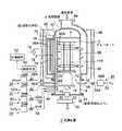
以下に、本発明に係る成膜方法、成膜装置及び記憶媒体の一実施例を添付図面に基づいて詳述する。
図1は本発明の係る成膜装置の一例を示す縦断面構成図、図2は成膜装置(加熱手段は省略)を示す横断面構成図である。尚、ここではシラン系ガスとしてジクロロシラン(DCS)を用い、窒化ガスとしてアンモニアガス(NH3 )を用い、ボロン含有ガスとしてBCl3 ガスを用い、炭化水素ガスとしてC2 H4 ガス(エチレンガス)を用い、上記NH3 ガスをプラズマにより活性化して炭素含有の各種膜を成膜する場合を例にとって説明する。またここでは後述する本発明方法の各実施例で用いられる全てのガス供給手段について説明するが、実施例によっては用いないガス種もあり、そのような実施例を行う場合には当該ガスのガス供給手段は不要になるのは勿論である。Hereinafter, an embodiment of a film forming method, a film forming apparatus, and a storage medium according to the present invention will be described in detail with reference to the accompanying drawings.
FIG. 1 is a longitudinal sectional view showing an example of a film forming apparatus according to the present invention, and FIG. 2 is a transverse sectional view showing a film forming apparatus (heating means is omitted). Here, dichlorosilane (DCS) is used as the silane gas, ammonia gas (NH3 ) is used as the nitriding gas, BCl3 gas is used as the boron-containing gas, and C2 H4 gas (ethylene gas) is used as the hydrocarbon gas. ) And the NH3 gas is activated by plasma to form various carbon-containing films. In addition, all gas supply means used in each embodiment of the method of the present invention to be described later will be described. However, depending on the embodiment, there are gas types that are not used. Of course, the supply means becomes unnecessary.
図示するように、プラズマを形成することができるこの成膜装置2は、下端が開口された有天井の円筒体状の処理容器4を有している。この処理容器4の全体は、例えば石英により形成されており、この処理容器4内の天井には、石英製の天井板6が設けられて封止されている。また、この処理容器4の下端開口部には、例えばステンレススチールにより円筒体状に成形されたマニホールド8がOリング等のシール部材10を介して連結されている。尚、ステンレス製のマニホールド8を設けないで、全体を円筒体状の石英製の処理容器で構成した装置もある。
上記処理容器4の下端は、上記マニホールド8によって支持されており、このマニホールド8の下方より多数枚の被処理体としての半導体ウエハWを多段に載置した保持手段としての石英製のウエハボート12が昇降可能に挿脱自在になされている。本実施例の場合において、このウエハボート12の支柱12Aには、例えば50〜100枚程度の直径が300mmのウエハWを略等ピッチで多段に支持できるようになっている。As shown in the figure, this
The lower end of the processing vessel 4 is supported by the
このウエハボート12は、石英製の保温筒14を介してテーブル16上に載置されており、このテーブル16は、マニホールド8の下端開口部を開閉する例えばステンレススチール製の蓋部18を貫通する回転軸20上に支持される。
そして、この回転軸20の貫通部には、例えば磁性流体シール22が介設され、この回転軸20を気密にシールしつつ回転可能に支持している。また、蓋部18の周辺部とマニホールド8の下端部には、例えばOリング等よりなるシール部材24が介設されており、処理容器4内のシール性を保持している。
上記した回転軸20は、例えばボートエレベータ等の昇降機構(図示せず)に支持されたアーム26の先端に取り付けられており、ウエハボート12及び蓋部18等を一体的に昇降して処理容器4内へ挿脱できるようになされている。尚、上記テーブル16を上記蓋部18側へ固定して設け、ウエハボート12を回転させることなくウエハWの処理を行うようにしてもよい。The
For example, a
The rotating
このマニホールド8には、処理容器4内の方へプラズマ化される窒化ガスとして、例えばアンモニア(NH3 )ガスを供給する窒化ガス供給手段28と、成膜ガスであるシラン系ガスとして例えばDCS(ジクロロシラン)ガスを供給するシラン系ガス供給手段30と、ボロン含有ガスとして例えばBCl3 ガスを供給するボロン含有ガス供給手段32と、炭化水素ガスとして例えばC2 H4 (エチレン)ガスを供給する炭化水素ガス供給手段34と、パージガスとして不活性ガス、例えばN2 ガスを供給するパージガス供給手段36とが設けられる。具体的には、上記窒化ガス供給手段28は、上記マニホールド8の側壁を内側へ貫通して上方向へ屈曲されて延びる石英管よりなるガス分散ノズル38を有している。このガス分散ノズル38には、その長さ方向に沿って複数(多数)のガス噴射孔38Aが所定の間隔を隔てて形成されており、各ガス噴射孔38Aから水平方向に向けて略均一にアンモニアガスを噴射できるようになっている。In the
また同様に上記シラン系ガス供給手段30も、上記マニホールド8の側壁を内側へ貫通して上方向へ屈曲されて延びる石英管よりなるガス分散ノズル40を有している。このガス分散ノズル40には、その長さ方向に沿って複数(多数)のガス噴射孔40Aが所定の間隔を隔てて形成されており、各ガス噴射孔40Aから水平方向に向けて略均一にシラン系ガスであるDCSガスを噴射できるようになっている。また同様にボロン含有ガス供給手段32も、上記マニホールド8の側壁を内側へ貫通して上方向へ屈曲されて延びる石英管よりなるガス分散ノズル42を有している。このガス分散ノズル42には、上記シラン系ガスのガス分散ノズル40と同様にその長さ方向に沿って複数(多数)のガス噴射孔42A(図2参照)が所定の間隔を隔てて形成されており、各ガス噴射孔42Aから水平方向に向けて略均一にBCl3 ガスを噴射できるようになっている。Similarly, the silane-based gas supply means 30 also has a
また同様に炭化水素ガス供給手段34も、上記マニホールド8の側壁を内側へ貫通して上方向へ屈曲されて延びる石英管よりなるガス分散ノズル44を有している。このガス分散ノズル44には、上記シラン系ガスのガス分散ノズル44と同様にその長さ方向に沿って複数(多数)のガス噴射孔44A(図2参照)が所定の間隔を隔てて形成されており、各ガス噴射孔44Aから水平方向に向けて略均一にC2 H4 ガスを噴射できるようになっている。Similarly, the hydrocarbon gas supply means 34 also has a
尚、前述したように、これらの4つのガス種の内、後述する成膜処理に不要なガスがある場合には、そのような成膜処理をする時、そのガス供給手段は成膜装置に設けなくてよいのは勿論である。また同様に上記パージガス供給手段36は、上記マニホールド8の側壁を貫通して設けたガスノズル46を有している。上記各ノズル38、40、42、44、46には、それぞれのガス通路48、50、52、54、56が接続されている。そして、各ガス通路48、50、52、54、56には、それぞれ開閉弁48A、50A、52A、54A、56A及びマスフローコントローラのような流量制御器48B、50B、52B、54B、56Bが介設されており、NH3 ガス、DCSガス、BCl3 ガス、C2 H4 ガス及びN2 ガスをそれぞれ流量制御しつつ供給できるようになっている。これらの各ガスの供給、供給停止、ガス流量の制御及び後述する高周波のオン・オフ制御等は例えばコンピュータ等よりなる制御手段60により行われる。またこの制御手段60は、上記制御に加え、この装置全体の動作も制御する。そして、この制御手段60は、上記制御を行うためのプログラムが記憶されているフロッピディスクやフラッシュメモリ等よりなる記憶媒体62を有している。As described above, when there is a gas unnecessary for the film forming process described later, among these four gas types, the gas supply means is connected to the film forming apparatus when performing such a film forming process. Of course, it is not necessary to provide it. Similarly, the purge gas supply means 36 has a
一方、上記処理容器4の側壁の一部には、その高さ方向に沿ってプラズマを発生させて窒化ガスを活性化させる活性化手段66が形成されると共に、この活性化手段66に対向する処理容器4の反対側には、この内部雰囲気を真空排気するために処理容器4の側壁を、例えば上下方向へ削りとることによって形成した細長い排気口68が設けられている。具体的には、上記活性化手段66は、上記処理容器4の側壁を上下方向に沿って所定の幅で削りとることによって上下に細長い開口70を形成し、この開口70をその外側より覆うようにして断面凹部状になされた上下に細長い例えば石英製のプラズマ区画壁72を容器外壁に気密に溶接接合することにより形成されている。これにより、この処理容器4の側壁の一部を凹部状に外側へ窪ませることにより一側が処理容器4内へ開口されて連通された活性化手段66が一体的に形成されることになる。すなわちプラズマ区画壁72の内部空間は、上記処理容器4内に一体的に連通された状態となっている。上記開口70は、ウエハボート12に保持されている全てのウエハWを高さ方向においてカバーできるように上下方向に十分に長く形成されている。 On the other hand, an activation means 66 that activates a nitriding gas by generating plasma along the height direction is formed on a part of the side wall of the processing vessel 4 and faces the activation means 66. On the opposite side of the processing container 4, there is provided an
そして、上記プラズマ区画壁72の両側壁の外側面には、その長さ方向(上下方向)に沿って互いに対向するようにして細長い一対のプラズマ電極74が設けられると共に、このプラズマ電極74にはプラズマ発生用の高周波電源76が給電ライン78を介して接続されており、上記プラズマ電極74に例えば13.56MHzの高周波電圧を印加することによりプラズマを発生し得るようになっている。尚、この高周波電圧の周波数は13.56MHzに限定されず、他の周波数、例えば400kHz等を用いてもよい。
そして、上記処理容器4内を上方向に延びていく窒化ガス用のガス分散ノズル38は途中で処理容器4の半径方向外方へ屈曲されて、上記プラズマ区画壁72内の一番奥(処理容器4の中心より一番離れた部分)に位置され、この一番奥の部分に沿って上方に向けて起立させて設けられている。従って、高周波電源76がオンされている時に上記ガス分散ノズル38のガス噴射孔38Aから噴射されたアンモニアガスはここで活性化されて処理容器4の中心に向けて拡散しつつ流れるようになっている。A pair of
Then, the
そして上記プラズマ区画壁72の外側には、これを覆うようにして例えば石英よりなる絶縁保護カバー80が取り付けられている。また、この絶縁保護カバー80の内側部分には、図示しない冷媒通路が設けられており、冷却された窒素ガスや冷却水を流すことにより上記プラズマ電極74を冷却し得るようになっている。
そして上記プラズマ区画壁72の開口70の外側近傍、すなわち開口70の外側(処理容器4内)には、上記シラン系ガス用のガス分散ノズル40とボロン含有ガス用のガス分散ノズル42と炭化水素ガス用のガス分散ノズル44とがそれぞれ起立させて設けられており、各ノズル40、42、44に設けた各ガス噴射孔40A、42A、44Aより処理容器4の中心方向に向けてシラン系ガスとBCl3 ガスとC2 H4 ガスとをそれぞれ噴射し得るようになっている。An insulating
In the vicinity of the outside of the
一方、上記開口70に対向させて設けた排気口68には、これを覆うようにして石英よりなる断面コ字状に成形された排気口カバー部材82が溶接により取り付けられている。この排気口カバー部材82は、上記処理容器4の側壁に沿って上方に延びており、処理容器4の上方のガス出口84より図示しない真空ポンプ等を介設した真空排気系により真空引きされる。そして、この処理容器4の外周を囲むようにしてこの処理容器4及びこの内部のウエハWを加熱する筒体状の加熱手段86が設けられている。 On the other hand, an exhaust
次に、以上のように構成された成膜装置2を用いて行なわれるプラズマによる本発明の成膜方法(いわゆるALD成膜)について説明する。
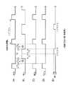
<成膜方法の第1実施例>
まず、本発明方法の第1実施例について説明する。
図3は本発明の成膜方法の第1実施例における各種ガスの供給のタイミングとRF(高周波)の印加タイミングを示すタイミングチャートである。この第1実施例では、シラン系ガス(DCS)と窒化ガス(NH3 )とボロン含有ガス(BCl3 )と炭化水素ガス(C2 H4 )を用いて半導体ウエハ上にSiBCN薄膜を形成する。すなわち、この第1実施例では、上記シラン系ガスとボロン含有ガスと炭化水素ガスの3種類のガスの同時供給と前記窒化ガスの供給とを間欠的に且つ交互に行うようにする。
まず、常温の多数枚、例えば50〜100枚の300mmサイズのウエハWが載置された状態のウエハボート12を予め所定の温度になされた処理容器4内にその下方より上昇させてロードし、蓋部18でマニホールド8の下端開口部を閉じることにより容器内を密閉する。Next, a film forming method (so-called ALD film forming) of the present invention using plasma performed using the
<First Example of Film Formation Method>
First, a first embodiment of the method of the present invention will be described.
FIG. 3 is a timing chart showing the supply timing of various gases and the application timing of RF (high frequency) in the first embodiment of the film forming method of the present invention. In this first embodiment, a SiBCN thin film is formed on a semiconductor wafer using a silane-based gas (DCS), a nitriding gas (NH3 ), a boron-containing gas (BCl3 ), and a hydrocarbon gas (C2 H4 ). . That is, in this first embodiment, the simultaneous supply of the three types of gas, the silane-based gas, the boron-containing gas, and the hydrocarbon gas, and the supply of the nitriding gas are performed intermittently and alternately.
First, a
そして処理容器4内を真空引きして所定のプロセス圧力に維持すると共に、加熱手段86への供給電力を増大させることにより、ウエハ温度を上昇させてプロセス温度を維持する。上記DCSガスをシラン系ガス供給手段30から供給し、BCl3 ガスをボロン含有ガス供給手段32から供給し、C2 H4 ガスを炭化水素ガス34から供給し、そして、NH3 ガスを窒化ガス供給手段28から供給する。具体的には、図3に示すように、DCSガスとBCl3 ガスとC2 H4 ガスの3種類のガスの同時供給と、NH3 ガスの供給とを間欠的に且つ交互に行うようにする。これにより、回転しているウエハボート12に支持されているウエハWの表面にSiBCN薄膜を形成する。この際、NH3 ガスを単独で供給する時に、全供給時間に亘って、或いは全供給時間の一部において高周波電源(RF電源)62をオンしてプラズマを立てるようにする。尚、図3(E)ではNH3 ガスの供給開始から所定時間経過してから高周波を印加するようにしている。Then, the inside of the processing container 4 is evacuated and maintained at a predetermined process pressure, and the power supplied to the heating means 86 is increased to raise the wafer temperature and maintain the process temperature. The DCS gas is supplied from the silane-based gas supply means 30, the BCl3 gas is supplied from the boron-containing gas supply means 32, the C2 H4 gas is supplied from the
具体的には、NH3 ガスはガス分散ノズル38の各ガス噴射孔38Aから水平方向へ噴射され、また、DCSガスはガス分散ノズル40の各ガス噴射孔40Aから水平方向へ噴射され、またBCl3 はガス分散ノズル42の各ガス噴射孔42Aから水平方向へ噴射され、またC2 H4 ガスはガス分散ノズル44の各ガス噴射孔44Aから水平方向へ噴射され、各ガスが反応してSiBCN薄膜が形成される。この場合、上記各ガスは、連続的に供給されるのではなく、図3に示すようにDCS、BCl3 及びC2 H4 ガスは同じタイミングで間欠的に、パルス状に供給する。NH3 ガスは上記3種類のガスの供給からタイミングをずらして上記3種のガスの供給停止の時に供給する。そして、タイミングをずらしたガス同士は、間に間欠期間(パージ期間)90を挟んで交互に間欠的に繰り返し供給され、SiBCN薄膜を一層ずつ繰り返し積層する。すなわち、図3(A)、図3(C)及び図3(D)に示すように、DCSとBCl3 とC2 H4 とは常に同時に、共通のタイミングで間欠的に供給される。これに対して、図3(B)に示すようにNH3 は上記DCS、BCl3 、C2 H4 ガスの供給休止期間の略中央にて単独で供給される。また間欠期間90においては真空引きが継続されて容器内に残留するガスを排除している。そして、NH3 ガスを単独で流す時には、図3(E)に示すようにRF電源がオンされてプラズマが立てられて、供給されるNH3 ガスを活性化して活性種等が作られ、反応(分解)が促進される。Specifically, NH3 gas is injected in the horizontal direction from each
この場合、NH3 ガスの供給期間の全期間に亘ってRF電源をオンしてもよいし、図3(B)及び図3(E)に示すようにNH3 ガスの供給開始から所定の時間Δtが経過した後に、RF電源をオンするようにしてもよい。この所定の時間ΔtとはNH3 ガスの流量が安定するまでの時間であり、例えば5秒程度である。このように、NH3 ガスの流量が安定化した後にRF電源をオンすることにより、ウエハWの面間方向(高さ方向)における活性種の濃度均一性を向上できる。また間欠期間90では、不活性ガスであるN2 ガスを処理容器4内へ供給して残留ガスを排除するようにしてもよいし(不活性ガスパージ)、或いは、全てのガスの供給を停止したまま真空引きを継続して行うことにより(バキュームとも称す)、処理容器4内の残留ガスを排除するようにしてもよい。更には、間欠期間90の前半はバキュームを行い、後半は不活性ガスパージを行うようにしてもよい。In this case, the RF power supply may be turned on over the entire NH3 gas supply period, or as shown in FIGS. 3B and 3E, a predetermined time from the start of supply of the NH3 gas. The RF power supply may be turned on after Δt has elapsed. The predetermined time Δt is a time until the flow rate of the NH3 gas is stabilized, and is about 5 seconds, for example. Thus, by turning on the RF power supply after the flow rate of the NH3 gas is stabilized, the concentration uniformity of the active species in the inter-plane direction (height direction) of the wafer W can be improved. In the
この場合、吸着工程であるDCS、BCl3 及びC2 H4 ガスの供給期間T1は10秒程度、反応工程(窒化工程)である単独のNH3 ガスの供給期間T2は20秒程度、パージ期間である間欠期間90の長さT3は5〜15秒程度、RF電源のオン時間T4は10秒程度であるが、これらの各時間は単に一例を示したに過ぎず、この数値に限定されない。通常、1サイクルによって形成される膜厚は1.1〜1.3Å/サイクル程度であるので、目標膜厚が例えば700Åであるならば、600サイクル程度繰り返し行うことになる。上記のように成膜処理を行うことにより、形成されるSiBCN薄膜の誘電率を非常に低くでき、且つそのドライエッチング時のエッチング耐性を大幅に向上させることができる。
その理由は、次のように考えられる。すなわち、一般的にはシリコン窒化膜(SiN)にボロンを添加するとエッチング耐性は劣化するが、上記実施例のように、更にNH3 ガスの供給時にプラズマでNH3 ガスを活性化させると窒化が促進される結果、Si−H結合が減少してエッチング耐性の強いSi−N結合が増加するからであると考えられる。In this case, the supply period T1 of DCS, BCl3 and C2 H4 gas as an adsorption process is about 10 seconds, the supply period T2 of a single NH3 gas as a reaction process (nitriding process) is about 20 seconds, and a purge period The length T3 of the
The reason is considered as follows. That is, generally, when boron is added to a silicon nitride film (SiN), the etching resistance is deteriorated. However, when NH3 gas is further activated by plasma when NH3 gas is supplied as in the above embodiment, nitridation occurs. As a result of promotion, it is considered that Si—H bonds are decreased and Si—N bonds having strong etching resistance are increased.
また、上記のように、シリコン窒化膜を成膜する際に、炭化水素ガスとして例えばC2 H4 ガスを処理容器8内へ供給することにより、ウエハ表面に形成される膜中に炭素成分が含有された状態となる。このように、膜中に炭素成分が含有されると、従来の成膜温度、例えば760℃程度よりも低い温度、例えば550℃で成膜したにもかかわらず、この表面のクリーニング処理時やエッチング処理時に用いられる希フッ酸に対するエッチングレートを小さくでき、この結果、クリーニング処理時にこの薄膜が過度に削り取られることを防止して、この膜厚の制御性を向上させることが可能となる。またエッチングストッパ膜や層間絶縁膜としての機能も十分に果すことができる。Further, as described above, when a silicon nitride film is formed, by supplying, for example, C2 H4 gas as a hydrocarbon gas into the
またDCSガスを間欠的に供給して間欠期間T3を間欠的に設けるようにしているので、各間欠期間T3の直前で成膜されたSiBCN膜の表面が間欠期間T3で改質されて膜質が向上するので、エッチングレートを一層抑制することができる。この間欠処理時の原子レベルの作用は次のように考えられる。すなわち、炭素原子を含有するSiBCN膜の成膜時には、この薄膜の最表面にDCSガス中の付着乃至堆積時に脱離できなかったCl原子が活性化状態で結合しているが、DCSガスの供給が停止される間欠期間T3を設けることで、この間欠期間T3においてC2 H4 ガスやNH3 ガス中のC原子やN原子が上記薄膜最表面のCl原子と置換されて膜中のCl成分が減少し、結果的にエッチングレートを抑制でき、特にC2 H4 ガスを用いることにより膜中に取り込まれるC原子の量が増加することとなるのでエッチングレートを一層抑制することが可能となる。
またシリコン窒化膜にボロンと炭素を添加すると、入れない場合と比較して成膜レートが20〜30%程度上げることができる。この理由は、炭素の添加によりウエハ表面に対するボロンの吸着が促進されるからである、と考えられる。Further, since the DCS gas is intermittently supplied and the intermittent period T3 is intermittently provided, the surface of the SiBCN film formed immediately before each intermittent period T3 is modified in the intermittent period T3, and the film quality is improved. Since it improves, an etching rate can be suppressed further. The action at the atomic level during this intermittent treatment is considered as follows. That is, at the time of forming a SiBCN film containing carbon atoms, Cl atoms that could not be detached during deposition or deposition in the DCS gas are bonded to the outermost surface of the thin film in an activated state. In the intermittent period T3, C atoms and N atoms in the C2 H4 gas and the NH3 gas are replaced with Cl atoms on the outermost surface of the thin film, thereby providing a Cl component in the film. As a result, the etching rate can be suppressed, and in particular, the amount of C atoms taken into the film is increased by using C2 H4 gas, so that the etching rate can be further suppressed. .
Further, when boron and carbon are added to the silicon nitride film, the film formation rate can be increased by about 20 to 30% as compared with the case where boron and carbon are not added. The reason for this is considered that the addition of carbon promotes the adsorption of boron to the wafer surface.
ここで上記成膜処理のプロセス条件について説明すると、DCSガスの流量は50〜2000sccmの範囲内、例えば1000sccm(1slm)であり、NH3 ガスの流量は500〜5000sccmの範囲内、例えば1000sccmであり、BCl3 ガスの流量は1〜15sccmの範囲内、例えば4sccmであり、C2 H4 ガスの流量は200〜2000sccmの範囲内、例えば500sccmである。ここでC2 H4 ガスの流量はDCSガスの流量の3倍以下である。その理由は、炭化水素ガスであるC2 H4 ガスの流量が過度に多過ぎると、膜質が急激に低下する、という不都合が生ずるからである。Here, the process conditions of the film forming process will be described. The flow rate of DCS gas is in the range of 50 to 2000 sccm, for example, 1000 sccm (1 slm), and the flow rate of NH3 gas is in the range of 500 to 5000 sccm, for example, 1000 sccm. The flow rate of BCl3 gas is in the range of 1-15 sccm, for example 4 sccm, and the flow rate of C2 H4 gas is in the range of 200-2000 sccm, for example 500 sccm. Here, the flow rate of the C2 H4 gas is not more than 3 times the flow rate of the DCS gas. The reason is that if the flow rate of the C2 H4 gas, which is a hydrocarbon gas, is excessively large, there is a disadvantage that the film quality deteriorates rapidly.
またプロセス温度はCVD成膜処理よりも低い温度であり、具体的には300〜700℃の範囲内、好ましくは550〜630℃の範囲内である。このプロセス温度が300℃よりも低いと、反応が生ぜずにほとんど膜が堆積せず、また700℃よりも高い場合には、膜質の劣るCVDによる堆積膜が形成されてしまうのみならず、前工程ですでに形成されている金属膜等に熱的ダメージを与えてしまう。
またプロセス圧力は13Pa(0.1Torr)〜13300Pa(100Torr)の範囲内、好ましくは40Pa(0.3Torr)〜266Pa(2Torr)の範囲内であり、例えば吸着工程では1Torr、プラズマを用いる窒化工程では0.3Torrである。ここでプロセス圧力が13Paよりも小さい場合には、成膜レートが実用レベル以下になってしまう。またプロセス圧力が13300Paまでは、ウエハWに対する反応は吸着反応が主流であるので、膜質が良好な薄膜を高い成膜速度で安定的に堆積させることができ、良好な結果を得ることができる。
しかし、プロセス圧力が13300Paよりも大きくなると、反応形態が吸着反応から気相反応へ移行してこの気相反応が主流となり、この結果、膜厚の面間及び面内均一性が低下するのみならず、気相反応に起因するパーティクルが急激に増大するので好ましくない。Further, the process temperature is lower than the CVD film forming treatment, and specifically, is in the range of 300 to 700 ° C, preferably in the range of 550 to 630 ° C. When the process temperature is lower than 300 ° C., no reaction occurs and almost no film is deposited. When the process temperature is higher than 700 ° C., not only a CVD deposited film with poor film quality is formed, but also The metal film already formed in the process will be thermally damaged.
The process pressure is in the range of 13 Pa (0.1 Torr) to 13300 Pa (100 Torr), preferably in the range of 40 Pa (0.3 Torr) to 266 Pa (2 Torr). For example, in the adsorption process, 1 Torr, in the nitriding process using plasma, 0.3 Torr. Here, when the process pressure is smaller than 13 Pa, the film forming rate becomes below the practical level. Further, since the reaction with respect to the wafer W is mainly an adsorption reaction up to a process pressure of 13300 Pa, a thin film having a good film quality can be stably deposited at a high film formation rate, and a good result can be obtained.
However, if the process pressure becomes higher than 13300 Pa, the reaction form shifts from an adsorption reaction to a gas phase reaction, and this gas phase reaction becomes the mainstream. As a result, only the inter-surface and in-plane uniformity of the film thickness decreases. In addition, the particles resulting from the gas phase reaction increase rapidly, which is not preferable.
<成膜方法の第2実施例>
次に本発明の成膜方法の第2実施例について説明する。
図4は本発明の成膜方法の第2実施例における各種ガスの供給のタイミングとRF(高周波)の印加タイミングを示すタイミングチャートである。
この第2実施例ではシラン系ガス(DCS)と窒化ガス(NH3 )と炭化水素ガス(C2 H4 )を用いて半導体ウエハ上にSiCN薄膜(炭素含有シリコン窒化膜)を形成する。すなわち、この第2実施例では、上記シラン系ガスと炭化水素ガスの2種類のガスの同時供給と前記窒化ガスの供給とを間欠的に且つ交互に行うようにする。<Second Example of Film Formation Method>
Next, a second embodiment of the film forming method of the present invention will be described.
FIG. 4 is a timing chart showing various gas supply timings and RF (high frequency) application timings in the second embodiment of the film forming method of the present invention.
In this second embodiment, a SiCN thin film (carbon-containing silicon nitride film) is formed on a semiconductor wafer using a silane-based gas (DCS), a nitriding gas (NH3 ), and a hydrocarbon gas (C2 H4 ). That is, in the second embodiment, the simultaneous supply of the two types of gas, the silane-based gas and the hydrocarbon gas, and the supply of the nitriding gas are performed intermittently and alternately.
この第2実施例は、先の図3に示す1実施例においてボロン含有ガスであるBCl3 ガスの供給を全く行わないようにして成膜を行った方法に対応するものであり、膜中にはボロン(B)が添加されていない。従って、この第2実施例を行う場合には、図1に示す成膜装置において、ボロン含有ガス供給手段32は不要となる。尚、この第2実施例のプロセス条件は、ボロン含有ガスに関する条件を除き、先の第1実施例の場合と同じである。
この第2実施例の場合にも、シリコン窒化膜中に炭素成分が含有されることになるので、第1実施例の場合と同様に、従来の成膜温度、例えば760℃程度よりも低い温度、例えば550℃で成膜したにもかかわらず、この表面のクリーニング処理時やエッチング処理時に用いられる希フッ酸に対するエッチングレートを小さくでき、この結果、クリーニング処理時にこの薄膜が過度に削り取られることを防止して、この膜厚の制御性を向上させることが可能となる。またエッチングストッパ膜や層間絶縁膜としての機能も十分に果すことができる。This second embodiment corresponds to a method in which film formation is performed in such a manner that the supply of BCl3 gas, which is a boron-containing gas, is not performed at all in the first embodiment shown in FIG. Boron (B) is not added. Therefore, when performing the second embodiment, the boron-containing gas supply means 32 is not necessary in the film forming apparatus shown in FIG. The process conditions of the second embodiment are the same as those of the first embodiment except for the conditions relating to the boron-containing gas.
Also in the case of the second embodiment, since the carbon component is contained in the silicon nitride film, similarly to the case of the first embodiment, a temperature lower than a conventional film forming temperature, for example, about 760 ° C. For example, despite the fact that the film was formed at 550 ° C., the etching rate for dilute hydrofluoric acid used during the cleaning process or etching process of the surface can be reduced, and as a result, the thin film is excessively scraped off during the cleaning process. Therefore, the controllability of the film thickness can be improved. Also, it can sufficiently function as an etching stopper film and an interlayer insulating film.
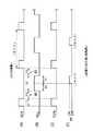
<成膜方法の第3実施例>
次に本発明の成膜方法の第3実施例について説明する。
図5は本発明の成膜方法の第3実施例における各種ガスの供給のタイミングとRF(高周波)の印加タイミングを示すタイミングチャートである。
この第3実施例では窒化ガス(NH3 )とボロン含有ガスと炭化水素ガス(C2 H4 )を用いて半導体ウエハ上にBCN薄膜(炭素含有ボロン窒化膜)を形成する。すなわち、この第3実施例では、上記ボロン含有ガスと炭化水素ガスの2種類のガスの同時供給と上記窒化ガスの供給とを間欠的に且つ交互に行うようにする。<Third Example of Film Formation Method>
Next, a third embodiment of the film forming method of the present invention will be described.
FIG. 5 is a timing chart showing various gas supply timings and RF (high frequency) application timings in the third embodiment of the film forming method of the present invention.
In the third embodiment, a BCN thin film (carbon-containing boron nitride film) is formed on a semiconductor wafer using a nitriding gas (NH3 ), a boron-containing gas, and a hydrocarbon gas (C2 H4 ). That is, in the third embodiment, the simultaneous supply of the two kinds of gases, the boron-containing gas and the hydrocarbon gas, and the supply of the nitriding gas are performed intermittently and alternately.
この第3実施例は、先の図3に示す第1実施例においてシラン系ガスであるDCSガスの供給を全く行わないようにして成膜を行った方法に対応するものであり、膜中にはSi(シラン)が添加されていない。従って、この第3実施例を行う場合には、図1に示す成膜装置において、シラン系ガス供給手段30は不要となる。尚、この第3実施例のプロセス条件は、シラン系ガスに関する条件を除き、先の第1実施例の場合と同じである。
この第3実施例の場合には、化学的性質がシリコンに似たボロンを用いてボロン窒化膜を形成しており、このボロン窒化膜中に炭素成分が含有されることになるので、第1実施例の場合と同様に、従来の成膜温度、例えば760℃程度よりも低い温度、例えば550℃で成膜したにもかかわらず、この表面のクリーニング処理時やエッチング処理時に用いられる希フッ酸に対するエッチングレートを小さくでき、この結果、クリーニング処理時にこの薄膜が過度に削り取られることを防止して、この膜厚の制御性を向上させることが可能となる。またエッチングストッパ膜や層間絶縁膜としての機能も十分に果すことができる。This third embodiment corresponds to a method in which film formation is performed without supplying DCS gas, which is a silane-based gas, in the first embodiment shown in FIG. No Si (silane) is added. Therefore, when the third embodiment is performed, the silane gas supply means 30 is not necessary in the film forming apparatus shown in FIG. The process conditions of the third embodiment are the same as those of the first embodiment except for the conditions relating to the silane-based gas.
In the case of the third embodiment, the boron nitride film is formed using boron having chemical properties similar to silicon, and the boron nitride film contains a carbon component. As in the case of the example, even though the film was formed at a temperature lower than the conventional film forming temperature, for example, about 760 ° C., for example, 550 ° C., dilute hydrofluoric acid used during the surface cleaning process or the etching process As a result, the thin film can be prevented from being excessively scraped off during the cleaning process, and the controllability of the film thickness can be improved. Also, it can sufficiently function as an etching stopper film and an interlayer insulating film.
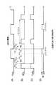
<成膜方法の第4実施例>
次に本発明の成膜方法の第4実施例について説明する。
図6は本発明の成膜方法の第4実施例における各種ガスの供給のタイミングとRF(高周波)の印加タイミングを示すタイミングチャート、図7は第4実施例で形成される薄膜の積層構造の一例を示す断面図である。
この第4実施例ではシラン系ガス(DCS)と窒化ガス(NH3 )とボロン含有ガス(BCl3 )と炭化水素ガス(C2 H4 )を用いて半導体ウエハ上に図7に示すようにSiBN薄膜92とSiCN薄膜94の繰り返し積層構造を形成する。尚、上記SiBN薄膜92とSiCN薄膜94は、少なくとも共に一層形成すればよい。すなわち、この第4実施例では、上記シラン系ガスとボロン含有ガスの2種類のガスを短時間だけ同時供給する第1工程と、上記窒化ガスを短時間だけ供給してSiBN薄膜を形成する第2工程と、上記シラン系ガスと炭化水素ガスの2種類のガスを短時間だけ同時供給する第3工程と、上記窒化ガスを短時間だけ供給してSiCN薄膜を形成する第4工程とを、上記順序に従って1回、または複数回繰り返し行うようにする。<Fourth Example of Film Formation Method>
Next, a fourth embodiment of the film forming method of the present invention will be described.
FIG. 6 is a timing chart showing various gas supply timings and RF (radio frequency) application timings in the fourth embodiment of the film forming method of the present invention, and FIG. 7 shows a laminated structure of thin films formed in the fourth embodiment. It is sectional drawing which shows an example.
In the fourth embodiment, a silane-based gas (DCS), a nitriding gas (NH3 ), a boron-containing gas (BCl3 ), and a hydrocarbon gas (C2 H4 ) are used on a semiconductor wafer as shown in FIG. A repeated stacked structure of the SiBN
この第4実施例は、先の図3に示す第1実施例において炭化水素ガスであるC2 H4 ガスの供給を全く行わない成膜方法の1サイクルと図4に示す第2実施例の成膜方法の1サイクルとを連結(連続)して新たな1サイクルとし、この新たな1サイクルを1回、或いは複数回繰り返すようにして成膜を行った方法である。図7は3サイクルの処理を行った時の状態を示している。尚、この第4実施例のプロセス条件は、炭化水素ガスに関する条件を除いた先の第1実施例と先の第2実施例の場合と同じである。
この第4実施例の場合には、図7に示すように、SiBN薄膜92とSiCN薄膜94とが交互に1回、または複数層重ねられた積層構造となるので、積層構造全体から見ればSiBCN薄膜と似た特性を示すことになる。In the fourth embodiment, one cycle of the film forming method in which the C2 H4 gas as the hydrocarbon gas is not supplied at all in the first embodiment shown in FIG. 3 and the second embodiment shown in FIG. This is a method in which film formation is performed by connecting (continuing) one cycle of the film formation method to a new cycle, and repeating this new cycle once or a plurality of times. FIG. 7 shows a state when three cycles of processing are performed. The process conditions of the fourth embodiment are the same as those of the first embodiment and the second embodiment except for the conditions relating to the hydrocarbon gas.
In the case of the fourth embodiment, as shown in FIG. 7, since the SiBN
この第4実施例の場合にも、シリコン窒化膜中に炭素成分やボロン成分が含有されることになるので、第1実施例の場合と同様に、従来の成膜温度、例えば760℃程度よりも低い温度、例えば550℃で成膜したにもかかわらず、この表面のクリーニング処理時やエッチング処理時に用いられる希フッ酸に対するエッチングレートを小さくでき、この結果、クリーニング処理時にこの薄膜が過度に削り取られることを防止して、この膜厚の制御性を向上させることが可能となる。またエッチングストッパ膜や層間絶縁膜としての機能も十分に果すことができる。また、ボロン元素も含有されるので、そのエッチング耐性を一層向上させることができる。 Also in the case of the fourth embodiment, since a carbon component and a boron component are contained in the silicon nitride film, similarly to the case of the first embodiment, the conventional film formation temperature, for example, about 760 ° C. Although the film is formed at a low temperature, for example, 550 ° C., the etching rate for dilute hydrofluoric acid used during the surface cleaning process or the etching process can be reduced. As a result, the thin film is excessively scraped off during the cleaning process. It is possible to improve the controllability of the film thickness. Also, it can sufficiently function as an etching stopper film and an interlayer insulating film. Moreover, since boron element is contained, the etching resistance can be further improved.
<各実施例の評価>
次に、上記第1乃至第3実施例を用いて各薄膜を形成して評価を行ったので、その評価結果について説明する。
図8は第1乃至第3実施例により形成された各薄膜のエッチングレートの評価結果を示すグラフである。ここでは、第1〜第3実施例を用いて形成した薄膜としてSiBCN薄膜、SiCN薄膜及びBCN薄膜の各エッチングレートをそれぞれ示しており、併せて炭素(C)成分を含まない各薄膜のエッチングレートもそれぞれ基準として併記している。この評価を行うときの成膜温度は550℃であり、エッチング液としては1%の希釈フッ化水素水を用いた。<Evaluation of each example>
Next, since each thin film was formed and evaluated using the first to third embodiments, the evaluation result will be described.
FIG. 8 is a graph showing the evaluation results of the etching rate of each thin film formed by the first to third examples. Here, the etching rates of the SiBCN thin film, the SiCN thin film, and the BCN thin film are shown as the thin films formed using the first to third embodiments, respectively, and the etching rates of the respective thin films not containing the carbon (C) component are also shown. Are also listed as standards. The film forming temperature for this evaluation was 550 ° C., and 1% diluted hydrogen fluoride water was used as the etching solution.
図8から明らかなように、各膜中に炭素成分を入れた膜種の場合には、炭素成分を入れない膜種よりも全てエッチングレートを低下させることができ、膜質の改善を図れることが確認できた。例えばSiBCN薄膜はSiBN薄膜に対して13.8%改善することができ、SiCN薄膜はSiN薄膜に対して6.8%改善することができ、BCN薄膜はBN薄膜に対して48%改善することができ、これにより炭素を含有させることの有用性を確認することができた。 As is clear from FIG. 8, in the case of a film type in which a carbon component is included in each film, the etching rate can be lowered as compared with a film type in which no carbon component is included, and the film quality can be improved. It could be confirmed. For example, SiBCN thin film can improve 13.8% over SiBN thin film, SiCN thin film can improve 6.8% over SiN thin film, and BCN thin film can improve 48% over BN thin film. As a result, the usefulness of containing carbon could be confirmed.
上記各第1乃至第4実施例にあっては、プラズマによりNH3 ガスを活性化させて反応を促進させたが、NH3 ガスを活性化させないようにしてもよい。この場合には、プラズマを用いないことによるエネルギーの低下を補償するためにプロセス温度を少し上げて成膜処理を行うようにする。
また上記各実施例では、炭化水素ガスとしてはエチレンガスを用いたが、これに限定されず、アセチレン、エチレン、メタン、エタン、プロパン、ブタンよりなる群より選択される1または2以上のガスを用いることができる。In each of the first to fourth embodiments described above, the NH3 gas is activated by plasma to promote the reaction. However, the NH3 gas may not be activated. In this case, the film forming process is performed by slightly raising the process temperature in order to compensate for a decrease in energy caused by not using plasma.
In each of the above embodiments, ethylene gas is used as the hydrocarbon gas. However, the present invention is not limited to this, and one or more gases selected from the group consisting of acetylene, ethylene, methane, ethane, propane, and butane are used. Can be used.
また上記各実施例では、シラン系ガスとしてDCSガスを用いたが、これに限定されず、ジクロロシラン(DCS)、ヘキサクロロジシラン(HCD)、モノシラン[SiH4 ]、ジシラン[Si2 H6 ]、ヘキサメチルジシラザン(HMDS)、テトラクロロシラン(TCS)、ジシリルアミン(DSA)、トリシリルアミン(TSA)、ビスターシャルブチルアミノシラン(BTBAS)よりなる群より選択される1以上のガスを用いることができる。In each of the above embodiments, DCS gas is used as the silane-based gas. However, the present invention is not limited to this, and dichlorosilane (DCS), hexachlorodisilane (HCD), monosilane [SiH4 ], disilane [Si2 H6 ], One or more gases selected from the group consisting of hexamethyldisilazane (HMDS), tetrachlorosilane (TCS), disilylamine (DSA), trisilylamine (TSA), and binary butylaminosilane (BTBAS) can be used.
また、上記各実施例では、窒化ガスとしてNH3 ガスを用いたが、これに限定されず、アンモニア[NH3 ]、窒素[N2 ]、一酸化二窒素[N2 O]、一酸化窒素[NO]よりなる群より選択される1以上のガスを用いることができる。
また、上記各実施例では、ボロン含有ガスとしてBCl3 ガスを用いたが、これに限定されず、BCl3 、B2 H6 、BF3 、B(CH3 )3 よりなる群より選択される1以上のガスを用いることができる。
また被処理体としては、半導体ウエハに限定されず、ガラス基板やLCD基板等にも本発明を適用することができる。In each of the above embodiments, NH3 gas is used as the nitriding gas. However, the present invention is not limited to this. Ammonia [NH3 ], nitrogen [N2 ], dinitrogen monoxide [N2 O], and nitric oxide One or more gases selected from the group consisting of [NO] can be used.
In each of the above embodiments, BCl3 gas is used as the boron-containing gas. However, the gas is not limited to this, and is selected from the group consisting of BCl3 , B2 H6 , BF3 , and B (CH3 )3. One or more gases can be used.
The object to be processed is not limited to a semiconductor wafer, and the present invention can be applied to a glass substrate, an LCD substrate, and the like.
2 成膜装置
4 処理容器
12 ウエハボート(保持手段)
28 窒化ガス供給手段
30 シラン系ガス供給手段
32 ボロン含有ガス供給手段
34 炭化水素ガス供給手段
38,40,42,44 ガス分散ノズル
60 制御手段
62 記憶媒体
66 活性化手段
74 プラズマ電極
76 高周波電源
86 加熱手段
W 半導体ウエハ(被処理体)
2 Film deposition apparatus 4
28 Nitriding gas supply means 30 Silane-based gas supply means 32 Boron-containing gas supply means 34 Hydrocarbon gas supply means 38, 40, 42, 44
Claims (13)
Translated fromJapanese前記シラン系ガスとボロン含有ガスと炭化水素ガスの3種類のガスの同時供給と前記窒化ガスの供給とを間欠的に且つ交互に行うようにしたことを特徴とする成膜方法。A silane-based gas, a nitriding gas, a boron-containing gas, and a hydrocarbon gas are supplied into a processing container in which a plurality of objects to be processed are accommodated and evacuated, and a SiBCN thin film is formed on the surface of the object to be processed. In the film forming method to be formed,
A film forming method, wherein the simultaneous supply of the three types of gas, the silane-based gas, the boron-containing gas, and the hydrocarbon gas, and the supply of the nitriding gas are performed intermittently and alternately.
真空引き可能になされた縦型の筒体状の処理容器と、
前記被処理体を複数段に保持して前記処理容器内に挿脱される保持手段と、
前記処理容器の外周に設けられる加熱手段と、
前記処理容器内へシラン系ガスを供給するシラン系ガス供給手段と、
前記処理容器内へ窒化ガスを供給する窒化ガス供給手段と、
前記処理容器内へボロン含有ガスを供給するボロン含有ガス供給手段と、
前記処理容器内へ炭化水素ガスを供給する炭化水素ガス供給手段と、
前記窒化ガスを活性化する活性化手段と、
請求項1乃至10のいずれか一項に記載の成膜方法を実施するように制御する制御手段と、
を備えたことを特徴とする成膜装置。In a film forming apparatus for forming a predetermined thin film on an object to be processed,
A vertical cylindrical processing container made evacuated,
Holding means for holding the object to be processed in a plurality of stages and being inserted into and removed from the processing container;
Heating means provided on the outer periphery of the processing container;
A silane-based gas supply means for supplying a silane-based gas into the processing vessel;
Nitriding gas supply means for supplying a nitriding gas into the processing vessel;
Boron-containing gas supply means for supplying boron-containing gas into the processing vessel;
Hydrocarbon gas supply means for supplying hydrocarbon gas into the processing vessel;
Activating means for activating the nitriding gas;
And control meansthat controls to perform the film forming method according to any one of claims 1 to 10,
A film forming apparatus comprising:
請求項1乃至10のいずれか一項に記載の成膜方法を実施するように前記成膜装置を制御するプログラムを記憶することを特徴とする記憶媒体。A silane-based gas, a nitriding gas, a boron-containing gas, and a hydrocarbon gas are supplied into a processing container in which a plurality of objects to be processed are accommodated and evacuated, and a SiBCN thin film is formed on the surface of the object to be processed. When forming a thin film using a film forming apparatus to be formed,
Storage medium characterized by storing a program for controlling thepre KiNarumaku deviceto perform the film forming method according to any one of claims 1 to 10.
Priority Applications (4)
| Application Number | Priority Date | Filing Date | Title |
|---|---|---|---|
| JP2006004191AJP4258518B2 (en) | 2005-03-09 | 2006-01-11 | Film forming method, film forming apparatus, and storage medium |
| US11/368,481US7351668B2 (en) | 2005-03-09 | 2006-03-07 | Film formation method and apparatus for semiconductor process |
| TW095107826ATWI374481B (en) | 2005-03-09 | 2006-03-08 | Film formation method and apparatus for semiconductor process |
| KR1020060021536AKR100935257B1 (en) | 2005-03-09 | 2006-03-08 | Method and apparatus for film formation for semiconductor processing, and computer readable medium |
Applications Claiming Priority (2)
| Application Number | Priority Date | Filing Date | Title |
|---|---|---|---|
| JP2005066340 | 2005-03-09 | ||
| JP2006004191AJP4258518B2 (en) | 2005-03-09 | 2006-01-11 | Film forming method, film forming apparatus, and storage medium |
Related Child Applications (1)
| Application Number | Title | Priority Date | Filing Date |
|---|---|---|---|
| JP2008309157ADivisionJP4893729B2 (en) | 2005-03-09 | 2008-12-03 | Film forming method, film forming apparatus, and storage medium |
Publications (3)
| Publication Number | Publication Date |
|---|---|
| JP2006287194A JP2006287194A (en) | 2006-10-19 |
| JP2006287194A5 JP2006287194A5 (en) | 2006-12-28 |
| JP4258518B2true JP4258518B2 (en) | 2009-04-30 |
Family
ID=36971600
Family Applications (1)
| Application Number | Title | Priority Date | Filing Date |
|---|---|---|---|
| JP2006004191AActiveJP4258518B2 (en) | 2005-03-09 | 2006-01-11 | Film forming method, film forming apparatus, and storage medium |
Country Status (4)
| Country | Link |
|---|---|
| US (1) | US7351668B2 (en) |
| JP (1) | JP4258518B2 (en) |
| KR (1) | KR100935257B1 (en) |
| TW (1) | TWI374481B (en) |
Families Citing this family (432)
| Publication number | Priority date | Publication date | Assignee | Title |
|---|---|---|---|---|
| JP4403824B2 (en)* | 2003-05-26 | 2010-01-27 | 東京エレクトロン株式会社 | Method for forming silicon nitride film |
| JP4279176B2 (en)* | 2004-03-02 | 2009-06-17 | 株式会社アルバック | Method for forming silicon nitride film |
| JP4396547B2 (en)* | 2004-06-28 | 2010-01-13 | 東京エレクトロン株式会社 | Film forming method, film forming apparatus, and storage medium |
| JP4929932B2 (en)* | 2006-09-01 | 2012-05-09 | 東京エレクトロン株式会社 | Film forming method, film forming apparatus, and storage medium |
| US20080145536A1 (en)* | 2006-12-13 | 2008-06-19 | Applied Materials, Inc. | METHOD AND APPARATUS FOR LOW TEMPERATURE AND LOW K SiBN DEPOSITION |
| US20080213479A1 (en)* | 2007-02-16 | 2008-09-04 | Tokyo Electron Limited | SiCN film formation method and apparatus |
| JP4924437B2 (en)* | 2007-02-16 | 2012-04-25 | 東京エレクトロン株式会社 | Film forming method and film forming apparatus |
| US7651961B2 (en)* | 2007-03-30 | 2010-01-26 | Tokyo Electron Limited | Method for forming strained silicon nitride films and a device containing such films |
| JP2008294260A (en)* | 2007-05-25 | 2008-12-04 | Sony Corp | Semiconductor device and manufacturing method therefor, and laminate insulating film and forming method therefor |
| JP5151260B2 (en)* | 2007-06-11 | 2013-02-27 | 東京エレクトロン株式会社 | Film forming method and film forming apparatus |
| JP4470970B2 (en)* | 2007-07-31 | 2010-06-02 | 東京エレクトロン株式会社 | Plasma processing equipment |
| US7964442B2 (en)* | 2007-10-09 | 2011-06-21 | Applied Materials, Inc. | Methods to obtain low k dielectric barrier with superior etch resistivity |
| JP5228437B2 (en)* | 2007-10-19 | 2013-07-03 | 東京エレクトロン株式会社 | Processing device and method of using the same |
| JP4924395B2 (en) | 2007-12-07 | 2012-04-25 | 東京エレクトロン株式会社 | Processing apparatus and processing method |
| US20090159958A1 (en)* | 2007-12-20 | 2009-06-25 | Spansion Llc | Electronic device including a silicon nitride layer and a process of forming the same |
| JP5284182B2 (en)* | 2008-07-23 | 2013-09-11 | 株式会社日立国際電気 | Substrate processing apparatus and semiconductor device manufacturing method |
| US10378106B2 (en) | 2008-11-14 | 2019-08-13 | Asm Ip Holding B.V. | Method of forming insulation film by modified PEALD |
| JP5384291B2 (en) | 2008-11-26 | 2014-01-08 | 株式会社日立国際電気 | Semiconductor device manufacturing method, substrate processing method, and substrate processing apparatus |
| JP2010147139A (en)* | 2008-12-17 | 2010-07-01 | Hitachi Kokusai Electric Inc | Method of manufacturing semiconductor device and substrate processing apparatus |
| US9394608B2 (en) | 2009-04-06 | 2016-07-19 | Asm America, Inc. | Semiconductor processing reactor and components thereof |
| JP5223804B2 (en)* | 2009-07-22 | 2013-06-26 | 東京エレクトロン株式会社 | Film forming method and film forming apparatus |
| US8802201B2 (en) | 2009-08-14 | 2014-08-12 | Asm America, Inc. | Systems and methods for thin-film deposition of metal oxides using excited nitrogen-oxygen species |
| KR101732187B1 (en)* | 2009-09-03 | 2017-05-02 | 에이에스엠 저펜 가부시기가이샤 | METHOD OF FORMING CONFORMAL DIELECTRIC FILM HAVING Si-N BONDS BY PECVD |
| JP5466526B2 (en)* | 2010-02-15 | 2014-04-09 | 株式会社日立国際電気 | Semiconductor device manufacturing method, substrate processing apparatus, and program |
| JP5651451B2 (en)* | 2010-03-16 | 2015-01-14 | 株式会社日立国際電気 | Semiconductor device manufacturing method, substrate processing method, and substrate processing apparatus |
| US9257274B2 (en) | 2010-04-15 | 2016-02-09 | Lam Research Corporation | Gapfill of variable aspect ratio features with a composite PEALD and PECVD method |
| US9997357B2 (en) | 2010-04-15 | 2018-06-12 | Lam Research Corporation | Capped ALD films for doping fin-shaped channel regions of 3-D IC transistors |
| US9076646B2 (en) | 2010-04-15 | 2015-07-07 | Lam Research Corporation | Plasma enhanced atomic layer deposition with pulsed plasma exposure |
| US20110256734A1 (en) | 2010-04-15 | 2011-10-20 | Hausmann Dennis M | Silicon nitride films and methods |
| US9390909B2 (en) | 2013-11-07 | 2016-07-12 | Novellus Systems, Inc. | Soft landing nanolaminates for advanced patterning |
| US8956983B2 (en) | 2010-04-15 | 2015-02-17 | Novellus Systems, Inc. | Conformal doping via plasma activated atomic layer deposition and conformal film deposition |
| US9611544B2 (en) | 2010-04-15 | 2017-04-04 | Novellus Systems, Inc. | Plasma activated conformal dielectric film deposition |
| US8637411B2 (en) | 2010-04-15 | 2014-01-28 | Novellus Systems, Inc. | Plasma activated conformal dielectric film deposition |
| US9892917B2 (en) | 2010-04-15 | 2018-02-13 | Lam Research Corporation | Plasma assisted atomic layer deposition of multi-layer films for patterning applications |
| US9373500B2 (en) | 2014-02-21 | 2016-06-21 | Lam Research Corporation | Plasma assisted atomic layer deposition titanium oxide for conformal encapsulation and gapfill applications |
| JP5573772B2 (en)* | 2010-06-22 | 2014-08-20 | 東京エレクトロン株式会社 | Film forming method and film forming apparatus |
| US9685320B2 (en) | 2010-09-23 | 2017-06-20 | Lam Research Corporation | Methods for depositing silicon oxide |
| US8076250B1 (en)* | 2010-10-06 | 2011-12-13 | Applied Materials, Inc. | PECVD oxide-nitride and oxide-silicon stacks for 3D memory application |
| JP6151335B2 (en)* | 2011-01-14 | 2017-06-21 | 株式会社日立国際電気 | Semiconductor device manufacturing method, substrate processing apparatus, and program |
| JP5847566B2 (en)* | 2011-01-14 | 2016-01-27 | 株式会社日立国際電気 | Semiconductor device manufacturing method, substrate processing method, substrate processing apparatus, and program |
| US8647993B2 (en) | 2011-04-11 | 2014-02-11 | Novellus Systems, Inc. | Methods for UV-assisted conformal film deposition |
| US9312155B2 (en) | 2011-06-06 | 2016-04-12 | Asm Japan K.K. | High-throughput semiconductor-processing apparatus equipped with multiple dual-chamber modules |
| JP5699980B2 (en) | 2011-06-16 | 2015-04-15 | 東京エレクトロン株式会社 | Film forming method and film forming apparatus |
| US10854498B2 (en) | 2011-07-15 | 2020-12-01 | Asm Ip Holding B.V. | Wafer-supporting device and method for producing same |
| US20130023129A1 (en) | 2011-07-20 | 2013-01-24 | Asm America, Inc. | Pressure transmitter for a semiconductor processing environment |
| JP5723243B2 (en) | 2011-08-11 | 2015-05-27 | 東京エレクトロン株式会社 | Film forming method, semiconductor device manufacturing method including the same, film forming apparatus, and semiconductor device |
| US9165761B2 (en)* | 2011-08-25 | 2015-10-20 | Hitachi Kokusai Electric Inc. | Method for manufacturing semiconductor device, method for processing substrate, substrate processing apparatus and recording medium |
| DE102011112897A1 (en)* | 2011-09-06 | 2013-03-07 | Sentech Instruments Gmbh | Apparatus and method for coating a substrate |
| JP5741382B2 (en)* | 2011-09-30 | 2015-07-01 | 東京エレクトロン株式会社 | Thin film forming method and film forming apparatus |
| US9017481B1 (en) | 2011-10-28 | 2015-04-28 | Asm America, Inc. | Process feed management for semiconductor substrate processing |
| JP5806612B2 (en)* | 2011-12-27 | 2015-11-10 | 東京エレクトロン株式会社 | Method for forming silicon oxycarbonitride film |
| US8592328B2 (en) | 2012-01-20 | 2013-11-26 | Novellus Systems, Inc. | Method for depositing a chlorine-free conformal sin film |
| JP5758829B2 (en) | 2012-03-27 | 2015-08-05 | 東京エレクトロン株式会社 | Method for forming boron-containing silicon oxycarbonitride film and method for forming silicon oxycarbonitride film |
| JP5920242B2 (en) | 2012-06-02 | 2016-05-18 | 東京エレクトロン株式会社 | Film forming method and film forming apparatus |
| US9659799B2 (en) | 2012-08-28 | 2017-05-23 | Asm Ip Holding B.V. | Systems and methods for dynamic semiconductor process scheduling |
| US10714315B2 (en) | 2012-10-12 | 2020-07-14 | Asm Ip Holdings B.V. | Semiconductor reaction chamber showerhead |
| KR102207992B1 (en) | 2012-10-23 | 2021-01-26 | 램 리써치 코포레이션 | Sub-saturated atomic layer deposition and conformal film deposition |
| JP6538300B2 (en) | 2012-11-08 | 2019-07-03 | ノベラス・システムズ・インコーポレーテッドNovellus Systems Incorporated | Method for depositing a film on a sensitive substrate |
| SG2013083241A (en) | 2012-11-08 | 2014-06-27 | Novellus Systems Inc | Conformal film deposition for gapfill |
| US20160376700A1 (en) | 2013-02-01 | 2016-12-29 | Asm Ip Holding B.V. | System for treatment of deposition reactor |
| JP6129573B2 (en)* | 2013-02-13 | 2017-05-17 | 株式会社日立国際電気 | Semiconductor device manufacturing method, substrate processing apparatus, and program |
| JP5793170B2 (en)* | 2013-09-30 | 2015-10-14 | 株式会社日立国際電気 | Semiconductor device manufacturing method, substrate processing apparatus, and program |
| JP5687328B2 (en)* | 2013-12-11 | 2015-03-18 | 株式会社日立国際電気 | Semiconductor device manufacturing method, substrate processing apparatus, and program |
| US9214334B2 (en) | 2014-02-18 | 2015-12-15 | Lam Research Corporation | High growth rate process for conformal aluminum nitride |
| US10683571B2 (en) | 2014-02-25 | 2020-06-16 | Asm Ip Holding B.V. | Gas supply manifold and method of supplying gases to chamber using same |
| JP6291297B2 (en) | 2014-03-17 | 2018-03-14 | 東京エレクトロン株式会社 | Film forming method, film forming apparatus, and storage medium |
| US10167557B2 (en) | 2014-03-18 | 2019-01-01 | Asm Ip Holding B.V. | Gas distribution system, reactor including the system, and methods of using the same |
| US11015245B2 (en) | 2014-03-19 | 2021-05-25 | Asm Ip Holding B.V. | Gas-phase reactor and system having exhaust plenum and components thereof |
| JP6340251B2 (en) | 2014-05-30 | 2018-06-06 | 東京エレクトロン株式会社 | Method for forming SiCN film |
| US10858737B2 (en) | 2014-07-28 | 2020-12-08 | Asm Ip Holding B.V. | Showerhead assembly and components thereof |
| US9478411B2 (en) | 2014-08-20 | 2016-10-25 | Lam Research Corporation | Method to tune TiOx stoichiometry using atomic layer deposited Ti film to minimize contact resistance for TiOx/Ti based MIS contact scheme for CMOS |
| US9478438B2 (en) | 2014-08-20 | 2016-10-25 | Lam Research Corporation | Method and apparatus to deposit pure titanium thin film at low temperature using titanium tetraiodide precursor |
| US9890456B2 (en) | 2014-08-21 | 2018-02-13 | Asm Ip Holding B.V. | Method and system for in situ formation of gas-phase compounds |
| JP6347705B2 (en) | 2014-09-17 | 2018-06-27 | 株式会社日立国際電気 | Semiconductor device manufacturing method, substrate processing apparatus, and program |
| US9214333B1 (en) | 2014-09-24 | 2015-12-15 | Lam Research Corporation | Methods and apparatuses for uniform reduction of the in-feature wet etch rate of a silicon nitride film formed by ALD |
| US9657845B2 (en) | 2014-10-07 | 2017-05-23 | Asm Ip Holding B.V. | Variable conductance gas distribution apparatus and method |
| US10941490B2 (en) | 2014-10-07 | 2021-03-09 | Asm Ip Holding B.V. | Multiple temperature range susceptor, assembly, reactor and system including the susceptor, and methods of using the same |
| US9589790B2 (en) | 2014-11-24 | 2017-03-07 | Lam Research Corporation | Method of depositing ammonia free and chlorine free conformal silicon nitride film |
| US9564312B2 (en) | 2014-11-24 | 2017-02-07 | Lam Research Corporation | Selective inhibition in atomic layer deposition of silicon-containing films |
| KR102263121B1 (en) | 2014-12-22 | 2021-06-09 | 에이에스엠 아이피 홀딩 비.브이. | Semiconductor device and manufacuring method thereof |
| US10529542B2 (en) | 2015-03-11 | 2020-01-07 | Asm Ip Holdings B.V. | Cross-flow reactor and method |
| US10276355B2 (en) | 2015-03-12 | 2019-04-30 | Asm Ip Holding B.V. | Multi-zone reactor, system including the reactor, and method of using the same |
| US10566187B2 (en) | 2015-03-20 | 2020-02-18 | Lam Research Corporation | Ultrathin atomic layer deposition film accuracy thickness control |
| US9502238B2 (en) | 2015-04-03 | 2016-11-22 | Lam Research Corporation | Deposition of conformal films by atomic layer deposition and atomic layer etch |
| US10458018B2 (en) | 2015-06-26 | 2019-10-29 | Asm Ip Holding B.V. | Structures including metal carbide material, devices including the structures, and methods of forming same |
| US10600673B2 (en) | 2015-07-07 | 2020-03-24 | Asm Ip Holding B.V. | Magnetic susceptor to baseplate seal |
| US10526701B2 (en) | 2015-07-09 | 2020-01-07 | Lam Research Corporation | Multi-cycle ALD process for film uniformity and thickness profile modulation |
| US9601693B1 (en) | 2015-09-24 | 2017-03-21 | Lam Research Corporation | Method for encapsulating a chalcogenide material |
| US9960072B2 (en) | 2015-09-29 | 2018-05-01 | Asm Ip Holding B.V. | Variable adjustment for precise matching of multiple chamber cavity housings |
| US11244822B2 (en)* | 2015-10-20 | 2022-02-08 | Taiwan Semiconductor Manufacturing Co., Ltd. | Apparatus for manufacturing a thin film and a method therefor |
| US10211308B2 (en) | 2015-10-21 | 2019-02-19 | Asm Ip Holding B.V. | NbMC layers |
| US9786492B2 (en)* | 2015-11-12 | 2017-10-10 | Asm Ip Holding B.V. | Formation of SiOCN thin films |
| US9786491B2 (en) | 2015-11-12 | 2017-10-10 | Asm Ip Holding B.V. | Formation of SiOCN thin films |
| US11139308B2 (en) | 2015-12-29 | 2021-10-05 | Asm Ip Holding B.V. | Atomic layer deposition of III-V compounds to form V-NAND devices |
| JP6523186B2 (en)* | 2016-02-01 | 2019-05-29 | 株式会社Kokusai Electric | Semiconductor device manufacturing method, substrate processing apparatus and program |
| US10529554B2 (en) | 2016-02-19 | 2020-01-07 | Asm Ip Holding B.V. | Method for forming silicon nitride film selectively on sidewalls or flat surfaces of trenches |
| US10468251B2 (en) | 2016-02-19 | 2019-11-05 | Asm Ip Holding B.V. | Method for forming spacers using silicon nitride film for spacer-defined multiple patterning |
| WO2017149604A1 (en)* | 2016-02-29 | 2017-09-08 | 株式会社日立国際電気 | Method for manufacturing semiconductor device, substrate processing apparatus, and recording medium |
| US10343920B2 (en) | 2016-03-18 | 2019-07-09 | Asm Ip Holding B.V. | Aligned carbon nanotubes |
| US10865475B2 (en) | 2016-04-21 | 2020-12-15 | Asm Ip Holding B.V. | Deposition of metal borides and silicides |
| US10190213B2 (en) | 2016-04-21 | 2019-01-29 | Asm Ip Holding B.V. | Deposition of metal borides |
| US10032628B2 (en) | 2016-05-02 | 2018-07-24 | Asm Ip Holding B.V. | Source/drain performance through conformal solid state doping |
| US10367080B2 (en) | 2016-05-02 | 2019-07-30 | Asm Ip Holding B.V. | Method of forming a germanium oxynitride film |
| KR102378021B1 (en) | 2016-05-06 | 2022-03-23 | 에이에스엠 아이피 홀딩 비.브이. | Formation of SiOC thin films |
| US11453943B2 (en) | 2016-05-25 | 2022-09-27 | Asm Ip Holding B.V. | Method for forming carbon-containing silicon/metal oxide or nitride film by ALD using silicon precursor and hydrocarbon precursor |
| US10388509B2 (en) | 2016-06-28 | 2019-08-20 | Asm Ip Holding B.V. | Formation of epitaxial layers via dislocation filtering |
| US9773643B1 (en) | 2016-06-30 | 2017-09-26 | Lam Research Corporation | Apparatus and method for deposition and etch in gap fill |
| US10062563B2 (en) | 2016-07-01 | 2018-08-28 | Lam Research Corporation | Selective atomic layer deposition with post-dose treatment |
| US9859151B1 (en) | 2016-07-08 | 2018-01-02 | Asm Ip Holding B.V. | Selective film deposition method to form air gaps |
| US10612137B2 (en) | 2016-07-08 | 2020-04-07 | Asm Ip Holdings B.V. | Organic reactants for atomic layer deposition |
| US10714385B2 (en) | 2016-07-19 | 2020-07-14 | Asm Ip Holding B.V. | Selective deposition of tungsten |
| US10395919B2 (en) | 2016-07-28 | 2019-08-27 | Asm Ip Holding B.V. | Method and apparatus for filling a gap |
| US9887082B1 (en) | 2016-07-28 | 2018-02-06 | Asm Ip Holding B.V. | Method and apparatus for filling a gap |
| US9812320B1 (en) | 2016-07-28 | 2017-11-07 | Asm Ip Holding B.V. | Method and apparatus for filling a gap |
| KR102532607B1 (en) | 2016-07-28 | 2023-05-15 | 에이에스엠 아이피 홀딩 비.브이. | Substrate processing apparatus and method of operating the same |
| US10629435B2 (en) | 2016-07-29 | 2020-04-21 | Lam Research Corporation | Doped ALD films for semiconductor patterning applications |
| US10037884B2 (en) | 2016-08-31 | 2018-07-31 | Lam Research Corporation | Selective atomic layer deposition for gapfill using sacrificial underlayer |
| US10074543B2 (en) | 2016-08-31 | 2018-09-11 | Lam Research Corporation | High dry etch rate materials for semiconductor patterning applications |
| US9865455B1 (en) | 2016-09-07 | 2018-01-09 | Lam Research Corporation | Nitride film formed by plasma-enhanced and thermal atomic layer deposition process |
| US10410943B2 (en) | 2016-10-13 | 2019-09-10 | Asm Ip Holding B.V. | Method for passivating a surface of a semiconductor and related systems |
| US10643826B2 (en) | 2016-10-26 | 2020-05-05 | Asm Ip Holdings B.V. | Methods for thermally calibrating reaction chambers |
| US11532757B2 (en) | 2016-10-27 | 2022-12-20 | Asm Ip Holding B.V. | Deposition of charge trapping layers |
| US10435790B2 (en) | 2016-11-01 | 2019-10-08 | Asm Ip Holding B.V. | Method of subatmospheric plasma-enhanced ALD using capacitively coupled electrodes with narrow gap |
| US10714350B2 (en) | 2016-11-01 | 2020-07-14 | ASM IP Holdings, B.V. | Methods for forming a transition metal niobium nitride film on a substrate by atomic layer deposition and related semiconductor device structures |
| US10229833B2 (en) | 2016-11-01 | 2019-03-12 | Asm Ip Holding B.V. | Methods for forming a transition metal nitride film on a substrate by atomic layer deposition and related semiconductor device structures |
| US10134757B2 (en) | 2016-11-07 | 2018-11-20 | Asm Ip Holding B.V. | Method of processing a substrate and a device manufactured by using the method |
| US10832908B2 (en) | 2016-11-11 | 2020-11-10 | Lam Research Corporation | Self-aligned multi-patterning process flow with ALD gapfill spacer mask |
| US10454029B2 (en) | 2016-11-11 | 2019-10-22 | Lam Research Corporation | Method for reducing the wet etch rate of a sin film without damaging the underlying substrate |
| US10134579B2 (en) | 2016-11-14 | 2018-11-20 | Lam Research Corporation | Method for high modulus ALD SiO2 spacer |
| KR102546317B1 (en) | 2016-11-15 | 2023-06-21 | 에이에스엠 아이피 홀딩 비.브이. | Gas supply unit and substrate processing apparatus including the same |
| US10340135B2 (en) | 2016-11-28 | 2019-07-02 | Asm Ip Holding B.V. | Method of topologically restricted plasma-enhanced cyclic deposition of silicon or metal nitride |
| KR102762543B1 (en) | 2016-12-14 | 2025-02-05 | 에이에스엠 아이피 홀딩 비.브이. | Substrate processing apparatus |
| US11447861B2 (en) | 2016-12-15 | 2022-09-20 | Asm Ip Holding B.V. | Sequential infiltration synthesis apparatus and a method of forming a patterned structure |
| US11581186B2 (en) | 2016-12-15 | 2023-02-14 | Asm Ip Holding B.V. | Sequential infiltration synthesis apparatus |
| KR102700194B1 (en) | 2016-12-19 | 2024-08-28 | 에이에스엠 아이피 홀딩 비.브이. | Substrate processing apparatus |
| US10269558B2 (en) | 2016-12-22 | 2019-04-23 | Asm Ip Holding B.V. | Method of forming a structure on a substrate |
| US10867788B2 (en) | 2016-12-28 | 2020-12-15 | Asm Ip Holding B.V. | Method of forming a structure on a substrate |
| US11390950B2 (en) | 2017-01-10 | 2022-07-19 | Asm Ip Holding B.V. | Reactor system and method to reduce residue buildup during a film deposition process |
| JP6857503B2 (en)* | 2017-02-01 | 2021-04-14 | 株式会社Kokusai Electric | Semiconductor device manufacturing methods, substrate processing devices and programs |
| US10655221B2 (en) | 2017-02-09 | 2020-05-19 | Asm Ip Holding B.V. | Method for depositing oxide film by thermal ALD and PEALD |
| US10468261B2 (en) | 2017-02-15 | 2019-11-05 | Asm Ip Holding B.V. | Methods for forming a metallic film on a substrate by cyclical deposition and related semiconductor device structures |
| US10529563B2 (en) | 2017-03-29 | 2020-01-07 | Asm Ip Holdings B.V. | Method for forming doped metal oxide films on a substrate by cyclical deposition and related semiconductor device structures |
| KR102457289B1 (en) | 2017-04-25 | 2022-10-21 | 에이에스엠 아이피 홀딩 비.브이. | Method for depositing a thin film and manufacturing a semiconductor device |
| CN114875388A (en) | 2017-05-05 | 2022-08-09 | Asm Ip 控股有限公司 | Plasma enhanced deposition method for controlled formation of oxygen-containing films |
| US10892156B2 (en) | 2017-05-08 | 2021-01-12 | Asm Ip Holding B.V. | Methods for forming a silicon nitride film on a substrate and related semiconductor device structures |
| US10446393B2 (en) | 2017-05-08 | 2019-10-15 | Asm Ip Holding B.V. | Methods for forming silicon-containing epitaxial layers and related semiconductor device structures |
| US10770286B2 (en) | 2017-05-08 | 2020-09-08 | Asm Ip Holdings B.V. | Methods for selectively forming a silicon nitride film on a substrate and related semiconductor device structures |
| US10504742B2 (en) | 2017-05-31 | 2019-12-10 | Asm Ip Holding B.V. | Method of atomic layer etching using hydrogen plasma |
| US10886123B2 (en) | 2017-06-02 | 2021-01-05 | Asm Ip Holding B.V. | Methods for forming low temperature semiconductor layers and related semiconductor device structures |
| US12040200B2 (en) | 2017-06-20 | 2024-07-16 | Asm Ip Holding B.V. | Semiconductor processing apparatus and methods for calibrating a semiconductor processing apparatus |
| US11306395B2 (en) | 2017-06-28 | 2022-04-19 | Asm Ip Holding B.V. | Methods for depositing a transition metal nitride film on a substrate by atomic layer deposition and related deposition apparatus |
| US10685834B2 (en) | 2017-07-05 | 2020-06-16 | Asm Ip Holdings B.V. | Methods for forming a silicon germanium tin layer and related semiconductor device structures |
| KR20190009245A (en) | 2017-07-18 | 2019-01-28 | 에이에스엠 아이피 홀딩 비.브이. | Methods for forming a semiconductor device structure and related semiconductor device structures |
| US11018002B2 (en) | 2017-07-19 | 2021-05-25 | Asm Ip Holding B.V. | Method for selectively depositing a Group IV semiconductor and related semiconductor device structures |
| US11374112B2 (en) | 2017-07-19 | 2022-06-28 | Asm Ip Holding B.V. | Method for depositing a group IV semiconductor and related semiconductor device structures |
| US10541333B2 (en) | 2017-07-19 | 2020-01-21 | Asm Ip Holding B.V. | Method for depositing a group IV semiconductor and related semiconductor device structures |
| US10590535B2 (en) | 2017-07-26 | 2020-03-17 | Asm Ip Holdings B.V. | Chemical treatment, deposition and/or infiltration apparatus and method for using the same |
| US10605530B2 (en) | 2017-07-26 | 2020-03-31 | Asm Ip Holding B.V. | Assembly of a liner and a flange for a vertical furnace as well as the liner and the vertical furnace |
| TWI815813B (en) | 2017-08-04 | 2023-09-21 | 荷蘭商Asm智慧財產控股公司 | Showerhead assembly for distributing a gas within a reaction chamber |
| US10692741B2 (en) | 2017-08-08 | 2020-06-23 | Asm Ip Holdings B.V. | Radiation shield |
| US10770336B2 (en) | 2017-08-08 | 2020-09-08 | Asm Ip Holding B.V. | Substrate lift mechanism and reactor including same |
| US10249524B2 (en) | 2017-08-09 | 2019-04-02 | Asm Ip Holding B.V. | Cassette holder assembly for a substrate cassette and holding member for use in such assembly |
| US11769682B2 (en) | 2017-08-09 | 2023-09-26 | Asm Ip Holding B.V. | Storage apparatus for storing cassettes for substrates and processing apparatus equipped therewith |
| US11139191B2 (en) | 2017-08-09 | 2021-10-05 | Asm Ip Holding B.V. | Storage apparatus for storing cassettes for substrates and processing apparatus equipped therewith |
| USD900036S1 (en) | 2017-08-24 | 2020-10-27 | Asm Ip Holding B.V. | Heater electrical connector and adapter |
| US11830730B2 (en) | 2017-08-29 | 2023-11-28 | Asm Ip Holding B.V. | Layer forming method and apparatus |
| US11056344B2 (en) | 2017-08-30 | 2021-07-06 | Asm Ip Holding B.V. | Layer forming method |
| KR102491945B1 (en) | 2017-08-30 | 2023-01-26 | 에이에스엠 아이피 홀딩 비.브이. | Substrate processing apparatus |
| US11295980B2 (en) | 2017-08-30 | 2022-04-05 | Asm Ip Holding B.V. | Methods for depositing a molybdenum metal film over a dielectric surface of a substrate by a cyclical deposition process and related semiconductor device structures |
| KR102401446B1 (en) | 2017-08-31 | 2022-05-24 | 에이에스엠 아이피 홀딩 비.브이. | Substrate processing apparatus |
| US10269559B2 (en) | 2017-09-13 | 2019-04-23 | Lam Research Corporation | Dielectric gapfill of high aspect ratio features utilizing a sacrificial etch cap layer |
| US10607895B2 (en) | 2017-09-18 | 2020-03-31 | Asm Ip Holdings B.V. | Method for forming a semiconductor device structure comprising a gate fill metal |
| KR102630301B1 (en) | 2017-09-21 | 2024-01-29 | 에이에스엠 아이피 홀딩 비.브이. | Method of sequential infiltration synthesis treatment of infiltrateable material and structures and devices formed using same |
| US10844484B2 (en) | 2017-09-22 | 2020-11-24 | Asm Ip Holding B.V. | Apparatus for dispensing a vapor phase reactant to a reaction chamber and related methods |
| US10658205B2 (en) | 2017-09-28 | 2020-05-19 | Asm Ip Holdings B.V. | Chemical dispensing apparatus and methods for dispensing a chemical to a reaction chamber |
| US10403504B2 (en) | 2017-10-05 | 2019-09-03 | Asm Ip Holding B.V. | Method for selectively depositing a metallic film on a substrate |
| US10319588B2 (en) | 2017-10-10 | 2019-06-11 | Asm Ip Holding B.V. | Method for depositing a metal chalcogenide on a substrate by cyclical deposition |
| US10923344B2 (en) | 2017-10-30 | 2021-02-16 | Asm Ip Holding B.V. | Methods for forming a semiconductor structure and related semiconductor structures |
| US10910262B2 (en) | 2017-11-16 | 2021-02-02 | Asm Ip Holding B.V. | Method of selectively depositing a capping layer structure on a semiconductor device structure |
| KR102443047B1 (en) | 2017-11-16 | 2022-09-14 | 에이에스엠 아이피 홀딩 비.브이. | Method of processing a substrate and a device manufactured by the same |
| US11022879B2 (en) | 2017-11-24 | 2021-06-01 | Asm Ip Holding B.V. | Method of forming an enhanced unexposed photoresist layer |
| WO2019103613A1 (en) | 2017-11-27 | 2019-05-31 | Asm Ip Holding B.V. | A storage device for storing wafer cassettes for use with a batch furnace |
| CN111344522B (en) | 2017-11-27 | 2022-04-12 | 阿斯莫Ip控股公司 | Including clean mini-environment device |
| US10872771B2 (en) | 2018-01-16 | 2020-12-22 | Asm Ip Holding B. V. | Method for depositing a material film on a substrate within a reaction chamber by a cyclical deposition process and related device structures |
| KR102695659B1 (en) | 2018-01-19 | 2024-08-14 | 에이에스엠 아이피 홀딩 비.브이. | Method for depositing a gap filling layer by plasma assisted deposition |
| TWI799494B (en) | 2018-01-19 | 2023-04-21 | 荷蘭商Asm 智慧財產控股公司 | Deposition method |
| USD903477S1 (en) | 2018-01-24 | 2020-12-01 | Asm Ip Holdings B.V. | Metal clamp |
| US11018047B2 (en) | 2018-01-25 | 2021-05-25 | Asm Ip Holding B.V. | Hybrid lift pin |
| USD880437S1 (en) | 2018-02-01 | 2020-04-07 | Asm Ip Holding B.V. | Gas supply plate for semiconductor manufacturing apparatus |
| US10535516B2 (en) | 2018-02-01 | 2020-01-14 | Asm Ip Holdings B.V. | Method for depositing a semiconductor structure on a surface of a substrate and related semiconductor structures |
| US11081345B2 (en) | 2018-02-06 | 2021-08-03 | Asm Ip Holding B.V. | Method of post-deposition treatment for silicon oxide film |
| WO2019158960A1 (en) | 2018-02-14 | 2019-08-22 | Asm Ip Holding B.V. | A method for depositing a ruthenium-containing film on a substrate by a cyclical deposition process |
| US10896820B2 (en) | 2018-02-14 | 2021-01-19 | Asm Ip Holding B.V. | Method for depositing a ruthenium-containing film on a substrate by a cyclical deposition process |
| US10731249B2 (en) | 2018-02-15 | 2020-08-04 | Asm Ip Holding B.V. | Method of forming a transition metal containing film on a substrate by a cyclical deposition process, a method for supplying a transition metal halide compound to a reaction chamber, and related vapor deposition apparatus |
| KR102636427B1 (en) | 2018-02-20 | 2024-02-13 | 에이에스엠 아이피 홀딩 비.브이. | Substrate processing method and apparatus |
| US10658181B2 (en) | 2018-02-20 | 2020-05-19 | Asm Ip Holding B.V. | Method of spacer-defined direct patterning in semiconductor fabrication |
| US10975470B2 (en) | 2018-02-23 | 2021-04-13 | Asm Ip Holding B.V. | Apparatus for detecting or monitoring for a chemical precursor in a high temperature environment |
| US11473195B2 (en) | 2018-03-01 | 2022-10-18 | Asm Ip Holding B.V. | Semiconductor processing apparatus and a method for processing a substrate |
| CN112005343B (en) | 2018-03-02 | 2025-05-06 | 朗姆研究公司 | Selective deposition using hydrolysis |
| US11629406B2 (en) | 2018-03-09 | 2023-04-18 | Asm Ip Holding B.V. | Semiconductor processing apparatus comprising one or more pyrometers for measuring a temperature of a substrate during transfer of the substrate |
| US11114283B2 (en) | 2018-03-16 | 2021-09-07 | Asm Ip Holding B.V. | Reactor, system including the reactor, and methods of manufacturing and using same |
| KR102444707B1 (en) | 2018-03-26 | 2022-09-19 | 에스케이하이닉스 주식회사 | Semiconductor device with ultra low k spacer and method for fabricating the same |
| KR102646467B1 (en) | 2018-03-27 | 2024-03-11 | 에이에스엠 아이피 홀딩 비.브이. | Method of forming an electrode on a substrate and a semiconductor device structure including an electrode |
| US11230766B2 (en) | 2018-03-29 | 2022-01-25 | Asm Ip Holding B.V. | Substrate processing apparatus and method |
| US10510536B2 (en) | 2018-03-29 | 2019-12-17 | Asm Ip Holding B.V. | Method of depositing a co-doped polysilicon film on a surface of a substrate within a reaction chamber |
| US11088002B2 (en) | 2018-03-29 | 2021-08-10 | Asm Ip Holding B.V. | Substrate rack and a substrate processing system and method |
| KR102501472B1 (en) | 2018-03-30 | 2023-02-20 | 에이에스엠 아이피 홀딩 비.브이. | Substrate processing method |
| KR102600229B1 (en) | 2018-04-09 | 2023-11-10 | 에이에스엠 아이피 홀딩 비.브이. | Substrate supporting device, substrate processing apparatus including the same and substrate processing method |
| TWI811348B (en) | 2018-05-08 | 2023-08-11 | 荷蘭商Asm 智慧財產控股公司 | Methods for depositing an oxide film on a substrate by a cyclical deposition process and related device structures |
| US12025484B2 (en) | 2018-05-08 | 2024-07-02 | Asm Ip Holding B.V. | Thin film forming method |
| US12272527B2 (en) | 2018-05-09 | 2025-04-08 | Asm Ip Holding B.V. | Apparatus for use with hydrogen radicals and method of using same |
| KR20190129718A (en) | 2018-05-11 | 2019-11-20 | 에이에스엠 아이피 홀딩 비.브이. | Methods for forming a doped metal carbide film on a substrate and related semiconductor device structures |
| KR102596988B1 (en) | 2018-05-28 | 2023-10-31 | 에이에스엠 아이피 홀딩 비.브이. | Method of processing a substrate and a device manufactured by the same |
| JP6987021B2 (en)* | 2018-05-28 | 2021-12-22 | 東京エレクトロン株式会社 | Plasma processing equipment and plasma processing method |
| US11718913B2 (en) | 2018-06-04 | 2023-08-08 | Asm Ip Holding B.V. | Gas distribution system and reactor system including same |
| TWI840362B (en) | 2018-06-04 | 2024-05-01 | 荷蘭商Asm Ip私人控股有限公司 | Wafer handling chamber with moisture reduction |
| US11286562B2 (en) | 2018-06-08 | 2022-03-29 | Asm Ip Holding B.V. | Gas-phase chemical reactor and method of using same |
| KR102568797B1 (en) | 2018-06-21 | 2023-08-21 | 에이에스엠 아이피 홀딩 비.브이. | Substrate processing system |
| US10797133B2 (en) | 2018-06-21 | 2020-10-06 | Asm Ip Holding B.V. | Method for depositing a phosphorus doped silicon arsenide film and related semiconductor device structures |
| TWI873894B (en) | 2018-06-27 | 2025-02-21 | 荷蘭商Asm Ip私人控股有限公司 | Cyclic deposition methods for forming metal-containing material and films and structures including the metal-containing material |
| KR102854019B1 (en) | 2018-06-27 | 2025-09-02 | 에이에스엠 아이피 홀딩 비.브이. | Periodic deposition method for forming a metal-containing material and films and structures comprising the metal-containing material |
| KR102686758B1 (en) | 2018-06-29 | 2024-07-18 | 에이에스엠 아이피 홀딩 비.브이. | Method for depositing a thin film and manufacturing a semiconductor device |
| US10612136B2 (en) | 2018-06-29 | 2020-04-07 | ASM IP Holding, B.V. | Temperature-controlled flange and reactor system including same |
| US10388513B1 (en) | 2018-07-03 | 2019-08-20 | Asm Ip Holding B.V. | Method for depositing silicon-free carbon-containing film as gap-fill layer by pulse plasma-assisted deposition |
| US10755922B2 (en) | 2018-07-03 | 2020-08-25 | Asm Ip Holding B.V. | Method for depositing silicon-free carbon-containing film as gap-fill layer by pulse plasma-assisted deposition |
| US10767789B2 (en) | 2018-07-16 | 2020-09-08 | Asm Ip Holding B.V. | Diaphragm valves, valve components, and methods for forming valve components |
| US10483099B1 (en) | 2018-07-26 | 2019-11-19 | Asm Ip Holding B.V. | Method for forming thermally stable organosilicon polymer film |
| US11053591B2 (en) | 2018-08-06 | 2021-07-06 | Asm Ip Holding B.V. | Multi-port gas injection system and reactor system including same |
| US10883175B2 (en) | 2018-08-09 | 2021-01-05 | Asm Ip Holding B.V. | Vertical furnace for processing substrates and a liner for use therein |
| US10829852B2 (en) | 2018-08-16 | 2020-11-10 | Asm Ip Holding B.V. | Gas distribution device for a wafer processing apparatus |
| US11430674B2 (en) | 2018-08-22 | 2022-08-30 | Asm Ip Holding B.V. | Sensor array, apparatus for dispensing a vapor phase reactant to a reaction chamber and related methods |
| US11024523B2 (en) | 2018-09-11 | 2021-06-01 | Asm Ip Holding B.V. | Substrate processing apparatus and method |
| KR102707956B1 (en) | 2018-09-11 | 2024-09-19 | 에이에스엠 아이피 홀딩 비.브이. | Method for deposition of a thin film |
| US11049751B2 (en) | 2018-09-14 | 2021-06-29 | Asm Ip Holding B.V. | Cassette supply system to store and handle cassettes and processing apparatus equipped therewith |
| CN110970344B (en) | 2018-10-01 | 2024-10-25 | Asmip控股有限公司 | Substrate holding apparatus, system comprising the same and method of using the same |
| US11232963B2 (en) | 2018-10-03 | 2022-01-25 | Asm Ip Holding B.V. | Substrate processing apparatus and method |
| KR102592699B1 (en) | 2018-10-08 | 2023-10-23 | 에이에스엠 아이피 홀딩 비.브이. | Substrate support unit and apparatuses for depositing thin film and processing the substrate including the same |
| US10847365B2 (en) | 2018-10-11 | 2020-11-24 | Asm Ip Holding B.V. | Method of forming conformal silicon carbide film by cyclic CVD |
| US10811256B2 (en) | 2018-10-16 | 2020-10-20 | Asm Ip Holding B.V. | Method for etching a carbon-containing feature |
| KR102605121B1 (en) | 2018-10-19 | 2023-11-23 | 에이에스엠 아이피 홀딩 비.브이. | Substrate processing apparatus and substrate processing method |
| KR102546322B1 (en) | 2018-10-19 | 2023-06-21 | 에이에스엠 아이피 홀딩 비.브이. | Substrate processing apparatus and substrate processing method |
| USD948463S1 (en) | 2018-10-24 | 2022-04-12 | Asm Ip Holding B.V. | Susceptor for semiconductor substrate supporting apparatus |
| US10381219B1 (en) | 2018-10-25 | 2019-08-13 | Asm Ip Holding B.V. | Methods for forming a silicon nitride film |
| US12378665B2 (en) | 2018-10-26 | 2025-08-05 | Asm Ip Holding B.V. | High temperature coatings for a preclean and etch apparatus and related methods |
| US11087997B2 (en) | 2018-10-31 | 2021-08-10 | Asm Ip Holding B.V. | Substrate processing apparatus for processing substrates |
| KR102748291B1 (en) | 2018-11-02 | 2024-12-31 | 에이에스엠 아이피 홀딩 비.브이. | Substrate support unit and substrate processing apparatus including the same |
| US11572620B2 (en) | 2018-11-06 | 2023-02-07 | Asm Ip Holding B.V. | Methods for selectively depositing an amorphous silicon film on a substrate |
| US11031242B2 (en) | 2018-11-07 | 2021-06-08 | Asm Ip Holding B.V. | Methods for depositing a boron doped silicon germanium film |
| US10847366B2 (en) | 2018-11-16 | 2020-11-24 | Asm Ip Holding B.V. | Methods for depositing a transition metal chalcogenide film on a substrate by a cyclical deposition process |
| US10818758B2 (en) | 2018-11-16 | 2020-10-27 | Asm Ip Holding B.V. | Methods for forming a metal silicate film on a substrate in a reaction chamber and related semiconductor device structures |
| US10559458B1 (en) | 2018-11-26 | 2020-02-11 | Asm Ip Holding B.V. | Method of forming oxynitride film |
| US12040199B2 (en) | 2018-11-28 | 2024-07-16 | Asm Ip Holding B.V. | Substrate processing apparatus for processing substrates |
| US11217444B2 (en) | 2018-11-30 | 2022-01-04 | Asm Ip Holding B.V. | Method for forming an ultraviolet radiation responsive metal oxide-containing film |
| KR102636428B1 (en) | 2018-12-04 | 2024-02-13 | 에이에스엠 아이피 홀딩 비.브이. | A method for cleaning a substrate processing apparatus |
| US11158513B2 (en) | 2018-12-13 | 2021-10-26 | Asm Ip Holding B.V. | Methods for forming a rhenium-containing film on a substrate by a cyclical deposition process and related semiconductor device structures |
| TWI874340B (en) | 2018-12-14 | 2025-03-01 | 荷蘭商Asm Ip私人控股有限公司 | Method of forming device structure, structure formed by the method and system for performing the method |
| TWI866480B (en) | 2019-01-17 | 2024-12-11 | 荷蘭商Asm Ip 私人控股有限公司 | Methods of forming a transition metal containing film on a substrate by a cyclical deposition process |
| KR102727227B1 (en) | 2019-01-22 | 2024-11-07 | 에이에스엠 아이피 홀딩 비.브이. | Semiconductor processing device |
| CN111524788B (en) | 2019-02-01 | 2023-11-24 | Asm Ip私人控股有限公司 | Method for forming topologically selective films of silicon oxide |
| TWI845607B (en) | 2019-02-20 | 2024-06-21 | 荷蘭商Asm Ip私人控股有限公司 | Cyclical deposition method and apparatus for filling a recess formed within a substrate surface |
| KR102626263B1 (en) | 2019-02-20 | 2024-01-16 | 에이에스엠 아이피 홀딩 비.브이. | Cyclical deposition method including treatment step and apparatus for same |
| TWI838458B (en) | 2019-02-20 | 2024-04-11 | 荷蘭商Asm Ip私人控股有限公司 | Apparatus and methods for plug fill deposition in 3-d nand applications |
| TWI873122B (en) | 2019-02-20 | 2025-02-21 | 荷蘭商Asm Ip私人控股有限公司 | Method of filling a recess formed within a surface of a substrate, semiconductor structure formed according to the method, and semiconductor processing apparatus |
| TWI842826B (en) | 2019-02-22 | 2024-05-21 | 荷蘭商Asm Ip私人控股有限公司 | Substrate processing apparatus and method for processing substrate |
| US11742198B2 (en) | 2019-03-08 | 2023-08-29 | Asm Ip Holding B.V. | Structure including SiOCN layer and method of forming same |
| KR102858005B1 (en) | 2019-03-08 | 2025-09-09 | 에이에스엠 아이피 홀딩 비.브이. | Method for Selective Deposition of Silicon Nitride Layer and Structure Including Selectively-Deposited Silicon Nitride Layer |
| KR102782593B1 (en) | 2019-03-08 | 2025-03-14 | 에이에스엠 아이피 홀딩 비.브이. | Structure Including SiOC Layer and Method of Forming Same |
| JP7321730B2 (en)* | 2019-03-14 | 2023-08-07 | キオクシア株式会社 | Semiconductor device manufacturing method |
| JP2020167398A (en) | 2019-03-28 | 2020-10-08 | エーエスエム・アイピー・ホールディング・ベー・フェー | Door openers and substrate processing equipment provided with door openers |
| KR102809999B1 (en) | 2019-04-01 | 2025-05-19 | 에이에스엠 아이피 홀딩 비.브이. | Method of manufacturing semiconductor device |
| KR20200123380A (en) | 2019-04-19 | 2020-10-29 | 에이에스엠 아이피 홀딩 비.브이. | Layer forming method and apparatus |
| KR20200125453A (en) | 2019-04-24 | 2020-11-04 | 에이에스엠 아이피 홀딩 비.브이. | Gas-phase reactor system and method of using same |
| KR102726216B1 (en) | 2019-05-01 | 2024-11-04 | 램 리써치 코포레이션 | Modulated atomic layer deposition |
| US11289326B2 (en) | 2019-05-07 | 2022-03-29 | Asm Ip Holding B.V. | Method for reforming amorphous carbon polymer film |
| KR20200130121A (en) | 2019-05-07 | 2020-11-18 | 에이에스엠 아이피 홀딩 비.브이. | Chemical source vessel with dip tube |
| KR20200130652A (en) | 2019-05-10 | 2020-11-19 | 에이에스엠 아이피 홀딩 비.브이. | Method of depositing material onto a surface and structure formed according to the method |
| JP7612342B2 (en) | 2019-05-16 | 2025-01-14 | エーエスエム・アイピー・ホールディング・ベー・フェー | Wafer boat handling apparatus, vertical batch furnace and method |
| JP7598201B2 (en) | 2019-05-16 | 2024-12-11 | エーエスエム・アイピー・ホールディング・ベー・フェー | Wafer boat handling apparatus, vertical batch furnace and method |
| USD947913S1 (en) | 2019-05-17 | 2022-04-05 | Asm Ip Holding B.V. | Susceptor shaft |
| USD975665S1 (en) | 2019-05-17 | 2023-01-17 | Asm Ip Holding B.V. | Susceptor shaft |
| USD935572S1 (en) | 2019-05-24 | 2021-11-09 | Asm Ip Holding B.V. | Gas channel plate |
| CN112017936B (en)* | 2019-05-28 | 2024-05-31 | 东京毅力科创株式会社 | Plasma processing apparatus |
| KR102837863B1 (en) | 2019-06-04 | 2025-07-23 | 램 리써치 코포레이션 | Polymeric protective liner for reactive ion etching during patterning |
| USD922229S1 (en) | 2019-06-05 | 2021-06-15 | Asm Ip Holding B.V. | Device for controlling a temperature of a gas supply unit |
| KR20200141002A (en) | 2019-06-06 | 2020-12-17 | 에이에스엠 아이피 홀딩 비.브이. | Method of using a gas-phase reactor system including analyzing exhausted gas |
| JP2022534793A (en) | 2019-06-07 | 2022-08-03 | ラム リサーチ コーポレーション | In situ control of film properties during atomic layer deposition |
| KR20200141931A (en) | 2019-06-10 | 2020-12-21 | 에이에스엠 아이피 홀딩 비.브이. | Method for cleaning quartz epitaxial chambers |
| KR20200143254A (en) | 2019-06-11 | 2020-12-23 | 에이에스엠 아이피 홀딩 비.브이. | Method of forming an electronic structure using an reforming gas, system for performing the method, and structure formed using the method |
| USD944946S1 (en) | 2019-06-14 | 2022-03-01 | Asm Ip Holding B.V. | Shower plate |
| USD931978S1 (en) | 2019-06-27 | 2021-09-28 | Asm Ip Holding B.V. | Showerhead vacuum transport |
| KR20210005515A (en) | 2019-07-03 | 2021-01-14 | 에이에스엠 아이피 홀딩 비.브이. | Temperature control assembly for substrate processing apparatus and method of using same |
| JP7499079B2 (en) | 2019-07-09 | 2024-06-13 | エーエスエム・アイピー・ホールディング・ベー・フェー | Plasma device using coaxial waveguide and substrate processing method |
| CN112216646A (en) | 2019-07-10 | 2021-01-12 | Asm Ip私人控股有限公司 | Substrate supporting assembly and substrate processing device comprising same |
| KR20210010307A (en) | 2019-07-16 | 2021-01-27 | 에이에스엠 아이피 홀딩 비.브이. | Substrate processing apparatus |
| KR102860110B1 (en) | 2019-07-17 | 2025-09-16 | 에이에스엠 아이피 홀딩 비.브이. | Methods of forming silicon germanium structures |
| KR20210010816A (en) | 2019-07-17 | 2021-01-28 | 에이에스엠 아이피 홀딩 비.브이. | Radical assist ignition plasma system and method |
| US11643724B2 (en) | 2019-07-18 | 2023-05-09 | Asm Ip Holding B.V. | Method of forming structures using a neutral beam |
| KR20210010817A (en) | 2019-07-19 | 2021-01-28 | 에이에스엠 아이피 홀딩 비.브이. | Method of Forming Topology-Controlled Amorphous Carbon Polymer Film |
| TWI839544B (en) | 2019-07-19 | 2024-04-21 | 荷蘭商Asm Ip私人控股有限公司 | Method of forming topology-controlled amorphous carbon polymer film |
| TWI851767B (en) | 2019-07-29 | 2024-08-11 | 荷蘭商Asm Ip私人控股有限公司 | Methods for selective deposition utilizing n-type dopants and/or alternative dopants to achieve high dopant incorporation |
| CN112309900A (en) | 2019-07-30 | 2021-02-02 | Asm Ip私人控股有限公司 | Substrate processing apparatus |
| CN112309899A (en) | 2019-07-30 | 2021-02-02 | Asm Ip私人控股有限公司 | Substrate processing apparatus |
| US12169361B2 (en) | 2019-07-30 | 2024-12-17 | Asm Ip Holding B.V. | Substrate processing apparatus and method |
| US11587815B2 (en) | 2019-07-31 | 2023-02-21 | Asm Ip Holding B.V. | Vertical batch furnace assembly |
| US11587814B2 (en) | 2019-07-31 | 2023-02-21 | Asm Ip Holding B.V. | Vertical batch furnace assembly |
| US11227782B2 (en) | 2019-07-31 | 2022-01-18 | Asm Ip Holding B.V. | Vertical batch furnace assembly |
| CN112323048B (en) | 2019-08-05 | 2024-02-09 | Asm Ip私人控股有限公司 | Liquid level sensor for chemical source container |
| CN114207184A (en) | 2019-08-06 | 2022-03-18 | 朗姆研究公司 | Thermal Atomic Layer Deposition of Silicon-Containing Films |
| CN112342526A (en) | 2019-08-09 | 2021-02-09 | Asm Ip私人控股有限公司 | Heater assembly including cooling device and method of using same |
| USD965044S1 (en) | 2019-08-19 | 2022-09-27 | Asm Ip Holding B.V. | Susceptor shaft |
| USD965524S1 (en) | 2019-08-19 | 2022-10-04 | Asm Ip Holding B.V. | Susceptor support |
| JP2021031769A (en) | 2019-08-21 | 2021-03-01 | エーエスエム アイピー ホールディング ビー.ブイ. | Production apparatus of mixed gas of film deposition raw material and film deposition apparatus |
| USD940837S1 (en) | 2019-08-22 | 2022-01-11 | Asm Ip Holding B.V. | Electrode |
| USD979506S1 (en) | 2019-08-22 | 2023-02-28 | Asm Ip Holding B.V. | Insulator |
| KR20210024423A (en) | 2019-08-22 | 2021-03-05 | 에이에스엠 아이피 홀딩 비.브이. | Method for forming a structure with a hole |
| USD949319S1 (en) | 2019-08-22 | 2022-04-19 | Asm Ip Holding B.V. | Exhaust duct |
| USD930782S1 (en) | 2019-08-22 | 2021-09-14 | Asm Ip Holding B.V. | Gas distributor |
| KR20210024420A (en) | 2019-08-23 | 2021-03-05 | 에이에스엠 아이피 홀딩 비.브이. | Method for depositing silicon oxide film having improved quality by peald using bis(diethylamino)silane |
| US11286558B2 (en) | 2019-08-23 | 2022-03-29 | Asm Ip Holding B.V. | Methods for depositing a molybdenum nitride film on a surface of a substrate by a cyclical deposition process and related semiconductor device structures including a molybdenum nitride film |
| KR102806450B1 (en) | 2019-09-04 | 2025-05-12 | 에이에스엠 아이피 홀딩 비.브이. | Methods for selective deposition using a sacrificial capping layer |
| KR102733104B1 (en) | 2019-09-05 | 2024-11-22 | 에이에스엠 아이피 홀딩 비.브이. | Substrate processing apparatus |
| US11562901B2 (en) | 2019-09-25 | 2023-01-24 | Asm Ip Holding B.V. | Substrate processing method |
| CN112593212B (en) | 2019-10-02 | 2023-12-22 | Asm Ip私人控股有限公司 | Method for forming topologically selective silicon oxide film by cyclic plasma enhanced deposition process |
| TW202128273A (en) | 2019-10-08 | 2021-08-01 | 荷蘭商Asm Ip私人控股有限公司 | Gas injection system, reactor system, and method of depositing material on surface of substratewithin reaction chamber |
| KR20210042810A (en) | 2019-10-08 | 2021-04-20 | 에이에스엠 아이피 홀딩 비.브이. | Reactor system including a gas distribution assembly for use with activated species and method of using same |
| TWI846953B (en) | 2019-10-08 | 2024-07-01 | 荷蘭商Asm Ip私人控股有限公司 | Substrate processing device |
| TWI846966B (en) | 2019-10-10 | 2024-07-01 | 荷蘭商Asm Ip私人控股有限公司 | Method of forming a photoresist underlayer and structure including same |
| US12009241B2 (en) | 2019-10-14 | 2024-06-11 | Asm Ip Holding B.V. | Vertical batch furnace assembly with detector to detect cassette |
| TWI834919B (en) | 2019-10-16 | 2024-03-11 | 荷蘭商Asm Ip私人控股有限公司 | Method of topology-selective film formation of silicon oxide |
| US11637014B2 (en) | 2019-10-17 | 2023-04-25 | Asm Ip Holding B.V. | Methods for selective deposition of doped semiconductor material |
| KR102845724B1 (en) | 2019-10-21 | 2025-08-13 | 에이에스엠 아이피 홀딩 비.브이. | Apparatus and methods for selectively etching films |
| KR20210050453A (en) | 2019-10-25 | 2021-05-07 | 에이에스엠 아이피 홀딩 비.브이. | Methods for filling a gap feature on a substrate surface and related semiconductor structures |
| US11646205B2 (en) | 2019-10-29 | 2023-05-09 | Asm Ip Holding B.V. | Methods of selectively forming n-type doped material on a surface, systems for selectively forming n-type doped material, and structures formed using same |
| KR20210054983A (en) | 2019-11-05 | 2021-05-14 | 에이에스엠 아이피 홀딩 비.브이. | Structures with doped semiconductor layers and methods and systems for forming same |
| US11501968B2 (en) | 2019-11-15 | 2022-11-15 | Asm Ip Holding B.V. | Method for providing a semiconductor device with silicon filled gaps |
| KR102861314B1 (en) | 2019-11-20 | 2025-09-17 | 에이에스엠 아이피 홀딩 비.브이. | Method of depositing carbon-containing material on a surface of a substrate, structure formed using the method, and system for forming the structure |
| US11450529B2 (en) | 2019-11-26 | 2022-09-20 | Asm Ip Holding B.V. | Methods for selectively forming a target film on a substrate comprising a first dielectric surface and a second metallic surface |
| CN112951697B (en) | 2019-11-26 | 2025-07-29 | Asmip私人控股有限公司 | Substrate processing apparatus |
| CN120432376A (en) | 2019-11-29 | 2025-08-05 | Asm Ip私人控股有限公司 | Substrate processing apparatus |
| CN112885692B (en) | 2019-11-29 | 2025-08-15 | Asmip私人控股有限公司 | Substrate processing apparatus |
| JP7527928B2 (en) | 2019-12-02 | 2024-08-05 | エーエスエム・アイピー・ホールディング・ベー・フェー | Substrate processing apparatus and substrate processing method |
| KR20210070898A (en) | 2019-12-04 | 2021-06-15 | 에이에스엠 아이피 홀딩 비.브이. | Substrate processing apparatus |
| KR20210078405A (en) | 2019-12-17 | 2021-06-28 | 에이에스엠 아이피 홀딩 비.브이. | Method of forming vanadium nitride layer and structure including the vanadium nitride layer |
| KR20210080214A (en) | 2019-12-19 | 2021-06-30 | 에이에스엠 아이피 홀딩 비.브이. | Methods for filling a gap feature on a substrate and related semiconductor structures |
| JP7636892B2 (en) | 2020-01-06 | 2025-02-27 | エーエスエム・アイピー・ホールディング・ベー・フェー | Channeled Lift Pins |
| JP7730637B2 (en) | 2020-01-06 | 2025-08-28 | エーエスエム・アイピー・ホールディング・ベー・フェー | Gas delivery assembly, components thereof, and reactor system including same |
| US11993847B2 (en) | 2020-01-08 | 2024-05-28 | Asm Ip Holding B.V. | Injector |
| KR20210093163A (en) | 2020-01-16 | 2021-07-27 | 에이에스엠 아이피 홀딩 비.브이. | Method of forming high aspect ratio features |
| KR102675856B1 (en) | 2020-01-20 | 2024-06-17 | 에이에스엠 아이피 홀딩 비.브이. | Method of forming thin film and method of modifying surface of thin film |
| TWI889744B (en) | 2020-01-29 | 2025-07-11 | 荷蘭商Asm Ip私人控股有限公司 | Contaminant trap system, and baffle plate stack |
| TW202513845A (en) | 2020-02-03 | 2025-04-01 | 荷蘭商Asm Ip私人控股有限公司 | Semiconductor structures and methods for forming the same |
| KR20210100010A (en) | 2020-02-04 | 2021-08-13 | 에이에스엠 아이피 홀딩 비.브이. | Method and apparatus for transmittance measurements of large articles |
| US11776846B2 (en) | 2020-02-07 | 2023-10-03 | Asm Ip Holding B.V. | Methods for depositing gap filling fluids and related systems and devices |
| KR20210103956A (en) | 2020-02-13 | 2021-08-24 | 에이에스엠 아이피 홀딩 비.브이. | Substrate processing apparatus including light receiving device and calibration method of light receiving device |
| TW202146691A (en) | 2020-02-13 | 2021-12-16 | 荷蘭商Asm Ip私人控股有限公司 | Gas distribution assembly, shower plate assembly, and method of adjusting conductance of gas to reaction chamber |
| TWI855223B (en) | 2020-02-17 | 2024-09-11 | 荷蘭商Asm Ip私人控股有限公司 | Method for growing phosphorous-doped silicon layer |
| CN113410160A (en) | 2020-02-28 | 2021-09-17 | Asm Ip私人控股有限公司 | System specially used for cleaning parts |
| KR20210113043A (en) | 2020-03-04 | 2021-09-15 | 에이에스엠 아이피 홀딩 비.브이. | Alignment fixture for a reactor system |
| US11876356B2 (en) | 2020-03-11 | 2024-01-16 | Asm Ip Holding B.V. | Lockout tagout assembly and system and method of using same |
| KR20210116240A (en) | 2020-03-11 | 2021-09-27 | 에이에스엠 아이피 홀딩 비.브이. | Substrate handling device with adjustable joints |
| KR102775390B1 (en) | 2020-03-12 | 2025-02-28 | 에이에스엠 아이피 홀딩 비.브이. | Method for Fabricating Layer Structure Having Target Topological Profile |
| US12173404B2 (en) | 2020-03-17 | 2024-12-24 | Asm Ip Holding B.V. | Method of depositing epitaxial material, structure formed using the method, and system for performing the method |
| KR102755229B1 (en) | 2020-04-02 | 2025-01-14 | 에이에스엠 아이피 홀딩 비.브이. | Thin film forming method |
| TWI887376B (en) | 2020-04-03 | 2025-06-21 | 荷蘭商Asm Ip私人控股有限公司 | Method for manufacturing semiconductor device |
| TWI888525B (en) | 2020-04-08 | 2025-07-01 | 荷蘭商Asm Ip私人控股有限公司 | Apparatus and methods for selectively etching silcon oxide films |
| US11821078B2 (en) | 2020-04-15 | 2023-11-21 | Asm Ip Holding B.V. | Method for forming precoat film and method for forming silicon-containing film |
| KR20210128343A (en) | 2020-04-15 | 2021-10-26 | 에이에스엠 아이피 홀딩 비.브이. | Method of forming chromium nitride layer and structure including the chromium nitride layer |
| US11996289B2 (en) | 2020-04-16 | 2024-05-28 | Asm Ip Holding B.V. | Methods of forming structures including silicon germanium and silicon layers, devices formed using the methods, and systems for performing the methods |
| KR20210130646A (en) | 2020-04-21 | 2021-11-01 | 에이에스엠 아이피 홀딩 비.브이. | Method for processing a substrate |
| CN113555279A (en) | 2020-04-24 | 2021-10-26 | Asm Ip私人控股有限公司 | Methods of forming vanadium nitride-containing layers and structures comprising the same |
| KR20210132600A (en) | 2020-04-24 | 2021-11-04 | 에이에스엠 아이피 홀딩 비.브이. | Methods and systems for depositing a layer comprising vanadium, nitrogen, and a further element |
| TW202208671A (en) | 2020-04-24 | 2022-03-01 | 荷蘭商Asm Ip私人控股有限公司 | Methods of forming structures including vanadium boride and vanadium phosphide layers |
| KR20210132612A (en) | 2020-04-24 | 2021-11-04 | 에이에스엠 아이피 홀딩 비.브이. | Methods and apparatus for stabilizing vanadium compounds |
| KR102866804B1 (en) | 2020-04-24 | 2025-09-30 | 에이에스엠 아이피 홀딩 비.브이. | Vertical batch furnace assembly comprising a cooling gas supply |
| KR102783898B1 (en) | 2020-04-29 | 2025-03-18 | 에이에스엠 아이피 홀딩 비.브이. | Solid source precursor vessel |
| KR20210134869A (en) | 2020-05-01 | 2021-11-11 | 에이에스엠 아이피 홀딩 비.브이. | Fast FOUP swapping with a FOUP handler |
| JP7726664B2 (en) | 2020-05-04 | 2025-08-20 | エーエスエム・アイピー・ホールディング・ベー・フェー | Substrate processing system for processing a substrate |
| KR102788543B1 (en) | 2020-05-13 | 2025-03-27 | 에이에스엠 아이피 홀딩 비.브이. | Laser alignment fixture for a reactor system |
| TW202146699A (en) | 2020-05-15 | 2021-12-16 | 荷蘭商Asm Ip私人控股有限公司 | Method of forming a silicon germanium layer, semiconductor structure, semiconductor device, method of forming a deposition layer, and deposition system |
| KR20210143653A (en) | 2020-05-19 | 2021-11-29 | 에이에스엠 아이피 홀딩 비.브이. | Substrate processing apparatus |
| KR20210145079A (en) | 2020-05-21 | 2021-12-01 | 에이에스엠 아이피 홀딩 비.브이. | Flange and apparatus for processing substrates |
| KR102795476B1 (en) | 2020-05-21 | 2025-04-11 | 에이에스엠 아이피 홀딩 비.브이. | Structures including multiple carbon layers and methods of forming and using same |
| TWI873343B (en) | 2020-05-22 | 2025-02-21 | 荷蘭商Asm Ip私人控股有限公司 | Reaction system for forming thin film on substrate |
| KR20210146802A (en) | 2020-05-26 | 2021-12-06 | 에이에스엠 아이피 홀딩 비.브이. | Method for depositing boron and gallium containing silicon germanium layers |
| TWI876048B (en) | 2020-05-29 | 2025-03-11 | 荷蘭商Asm Ip私人控股有限公司 | Substrate processing device |
| TW202212620A (en) | 2020-06-02 | 2022-04-01 | 荷蘭商Asm Ip私人控股有限公司 | Apparatus for processing substrate, method of forming film, and method of controlling apparatus for processing substrate |
| TW202208659A (en) | 2020-06-16 | 2022-03-01 | 荷蘭商Asm Ip私人控股有限公司 | Method for depositing boron containing silicon germanium layers |
| TW202218133A (en) | 2020-06-24 | 2022-05-01 | 荷蘭商Asm Ip私人控股有限公司 | Method for forming a layer provided with silicon |
| TWI873359B (en) | 2020-06-30 | 2025-02-21 | 荷蘭商Asm Ip私人控股有限公司 | Substrate processing method |
| US12431354B2 (en) | 2020-07-01 | 2025-09-30 | Asm Ip Holding B.V. | Silicon nitride and silicon oxide deposition methods using fluorine inhibitor |
| TW202202649A (en) | 2020-07-08 | 2022-01-16 | 荷蘭商Asm Ip私人控股有限公司 | Substrate processing method |
| KR20220010438A (en) | 2020-07-17 | 2022-01-25 | 에이에스엠 아이피 홀딩 비.브이. | Structures and methods for use in photolithography |
| KR20220011092A (en) | 2020-07-20 | 2022-01-27 | 에이에스엠 아이피 홀딩 비.브이. | Method and system for forming structures including transition metal layers |
| TWI878570B (en) | 2020-07-20 | 2025-04-01 | 荷蘭商Asm Ip私人控股有限公司 | Method and system for depositing molybdenum layers |
| US12322591B2 (en) | 2020-07-27 | 2025-06-03 | Asm Ip Holding B.V. | Thin film deposition process |
| CN115735261A (en) | 2020-07-28 | 2023-03-03 | 朗姆研究公司 | Impurity reduction in silicon-containing films |
| KR20220021863A (en) | 2020-08-14 | 2022-02-22 | 에이에스엠 아이피 홀딩 비.브이. | Method for processing a substrate |
| US12040177B2 (en) | 2020-08-18 | 2024-07-16 | Asm Ip Holding B.V. | Methods for forming a laminate film by cyclical plasma-enhanced deposition processes |
| TW202228863A (en) | 2020-08-25 | 2022-08-01 | 荷蘭商Asm Ip私人控股有限公司 | Method for cleaning a substrate, method for selectively depositing, and reaction system |
| US11725280B2 (en) | 2020-08-26 | 2023-08-15 | Asm Ip Holding B.V. | Method for forming metal silicon oxide and metal silicon oxynitride layers |
| TW202229601A (en) | 2020-08-27 | 2022-08-01 | 荷蘭商Asm Ip私人控股有限公司 | Method of forming patterned structures, method of manipulating mechanical property, device structure, and substrate processing system |
| TW202217045A (en) | 2020-09-10 | 2022-05-01 | 荷蘭商Asm Ip私人控股有限公司 | Methods for depositing gap filing fluids and related systems and devices |
| USD990534S1 (en) | 2020-09-11 | 2023-06-27 | Asm Ip Holding B.V. | Weighted lift pin |
| KR20220036866A (en) | 2020-09-16 | 2022-03-23 | 에이에스엠 아이피 홀딩 비.브이. | Silicon oxide deposition method |
| USD1012873S1 (en) | 2020-09-24 | 2024-01-30 | Asm Ip Holding B.V. | Electrode for semiconductor processing apparatus |
| TWI889903B (en) | 2020-09-25 | 2025-07-11 | 荷蘭商Asm Ip私人控股有限公司 | Semiconductor processing method |
| US12009224B2 (en) | 2020-09-29 | 2024-06-11 | Asm Ip Holding B.V. | Apparatus and method for etching metal nitrides |
| KR20220045900A (en) | 2020-10-06 | 2022-04-13 | 에이에스엠 아이피 홀딩 비.브이. | Deposition method and an apparatus for depositing a silicon-containing material |
| CN114293174A (en) | 2020-10-07 | 2022-04-08 | Asm Ip私人控股有限公司 | Gas supply unit and substrate processing apparatus including the same |
| TW202229613A (en) | 2020-10-14 | 2022-08-01 | 荷蘭商Asm Ip私人控股有限公司 | Method of depositing material on stepped structure |
| TW202232565A (en) | 2020-10-15 | 2022-08-16 | 荷蘭商Asm Ip私人控股有限公司 | Method of manufacturing semiconductor device, and substrate treatment apparatus using ether-cat |
| TW202217037A (en) | 2020-10-22 | 2022-05-01 | 荷蘭商Asm Ip私人控股有限公司 | Method of depositing vanadium metal, structure, device and a deposition assembly |
| TW202223136A (en) | 2020-10-28 | 2022-06-16 | 荷蘭商Asm Ip私人控股有限公司 | Method for forming layer on substrate, and semiconductor processing system |
| TW202229620A (en) | 2020-11-12 | 2022-08-01 | 特文特大學 | Deposition system, method for controlling reaction condition, method for depositing |
| TW202229795A (en) | 2020-11-23 | 2022-08-01 | 荷蘭商Asm Ip私人控股有限公司 | A substrate processing apparatus with an injector |
| TW202235649A (en) | 2020-11-24 | 2022-09-16 | 荷蘭商Asm Ip私人控股有限公司 | Methods for filling a gap and related systems and devices |
| TW202235675A (en) | 2020-11-30 | 2022-09-16 | 荷蘭商Asm Ip私人控股有限公司 | Injector, and substrate processing apparatus |
| US12255053B2 (en) | 2020-12-10 | 2025-03-18 | Asm Ip Holding B.V. | Methods and systems for depositing a layer |
| TW202233884A (en) | 2020-12-14 | 2022-09-01 | 荷蘭商Asm Ip私人控股有限公司 | Method of forming structures for threshold voltage control |
| US11946137B2 (en) | 2020-12-16 | 2024-04-02 | Asm Ip Holding B.V. | Runout and wobble measurement fixtures |
| TW202232639A (en) | 2020-12-18 | 2022-08-16 | 荷蘭商Asm Ip私人控股有限公司 | Wafer processing apparatus with a rotatable table |
| TW202242184A (en) | 2020-12-22 | 2022-11-01 | 荷蘭商Asm Ip私人控股有限公司 | Precursor capsule, precursor vessel, vapor deposition assembly, and method of loading solid precursor into precursor vessel |
| TW202226899A (en) | 2020-12-22 | 2022-07-01 | 荷蘭商Asm Ip私人控股有限公司 | Plasma treatment device having matching box |
| TW202231903A (en) | 2020-12-22 | 2022-08-16 | 荷蘭商Asm Ip私人控股有限公司 | Transition metal deposition method, transition metal layer, and deposition assembly for depositing transition metal on substrate |
| JP7623082B2 (en)* | 2021-02-04 | 2025-01-28 | 東京エレクトロン株式会社 | Carbon film forming method and film forming apparatus |
| USD980814S1 (en) | 2021-05-11 | 2023-03-14 | Asm Ip Holding B.V. | Gas distributor for substrate processing apparatus |
| USD1023959S1 (en) | 2021-05-11 | 2024-04-23 | Asm Ip Holding B.V. | Electrode for substrate processing apparatus |
| USD980813S1 (en) | 2021-05-11 | 2023-03-14 | Asm Ip Holding B.V. | Gas flow control plate for substrate processing apparatus |
| USD981973S1 (en) | 2021-05-11 | 2023-03-28 | Asm Ip Holding B.V. | Reactor wall for substrate processing apparatus |
| USD990441S1 (en) | 2021-09-07 | 2023-06-27 | Asm Ip Holding B.V. | Gas flow control plate |
| USD1060598S1 (en) | 2021-12-03 | 2025-02-04 | Asm Ip Holding B.V. | Split showerhead cover |
| WO2024047713A1 (en)* | 2022-08-29 | 2024-03-07 | 株式会社Kokusai Electric | Substrate processing method, method for producing semiconductor device, substrate processing apparatus, and program |
Family Cites Families (26)
| Publication number | Priority date | Publication date | Assignee | Title |
|---|---|---|---|---|
| JPH0293071A (en) | 1988-09-29 | 1990-04-03 | Toshiba Corp | Method of forming thin film |
| JPH0499026A (en)* | 1990-08-06 | 1992-03-31 | Kawasaki Steel Corp | Semiconductor device |
| JPH0634974A (en) | 1992-07-20 | 1994-02-10 | Toshiba Lighting & Technol Corp | Lighting device and liquid crystal display device |
| JPH0645256A (en) | 1992-07-21 | 1994-02-18 | Rikagaku Kenkyusho | Method for supplying gas pulse and method forming for film using the same |
| JP3529989B2 (en)* | 1997-09-12 | 2004-05-24 | 株式会社東芝 | Film forming method and semiconductor device manufacturing method |
| EP1146555B1 (en)* | 1999-03-09 | 2007-12-12 | Tokyo Electron Limited | Production method for a semiconductor device |
| JP2000282241A (en)* | 1999-04-01 | 2000-10-10 | Matsushita Electric Ind Co Ltd | Manufacturing method of multilayer thin film |
| JP3348084B2 (en)* | 1999-12-28 | 2002-11-20 | キヤノン販売株式会社 | Film forming method and semiconductor device |
| JP2003045864A (en)* | 2001-08-02 | 2003-02-14 | Hitachi Kokusai Electric Inc | Substrate processing equipment |
| JP2003166060A (en)* | 2001-11-30 | 2003-06-13 | L'air Liquide Sa Pour L'etude & L'exploitation Des Procede S Georges Claude | Method for manufacturing silicon nitride film, silicon oxynitride film, or silicon oxide film by cvd method |
| JP2003218106A (en)* | 2002-01-23 | 2003-07-31 | Hitachi Kokusai Electric Inc | Method for manufacturing semiconductor device |
| KR100449028B1 (en) | 2002-03-05 | 2004-09-16 | 삼성전자주식회사 | Method for forming thin film using ALD |
| JP3947126B2 (en)* | 2002-04-11 | 2007-07-18 | 株式会社日立国際電気 | Semiconductor manufacturing equipment |
| US20050136657A1 (en)* | 2002-07-12 | 2005-06-23 | Tokyo Electron Limited | Film-formation method for semiconductor process |
| KR100981355B1 (en)* | 2002-10-11 | 2010-09-10 | 우수이 고쿠사이 산교 가부시키가이샤 | Fuel pipe |
| JP3574651B2 (en)* | 2002-12-05 | 2004-10-06 | 東京エレクトロン株式会社 | Film forming method and film forming apparatus |
| JP4259247B2 (en)* | 2003-09-17 | 2009-04-30 | 東京エレクトロン株式会社 | Deposition method |
| US7273818B2 (en)* | 2003-10-20 | 2007-09-25 | Tokyo Electron Limited | Film formation method and apparatus for semiconductor process |
| JP4655495B2 (en)* | 2004-03-31 | 2011-03-23 | 東京エレクトロン株式会社 | Deposition method |
| JP4675127B2 (en)* | 2004-04-23 | 2011-04-20 | 東京エレクトロン株式会社 | Thin film forming apparatus, thin film forming apparatus cleaning method and program |
| JP3945519B2 (en)* | 2004-06-21 | 2007-07-18 | 東京エレクトロン株式会社 | Heat treatment apparatus, heat treatment method and storage medium for object to be processed |
| JP4396547B2 (en)* | 2004-06-28 | 2010-01-13 | 東京エレクトロン株式会社 | Film forming method, film forming apparatus, and storage medium |
| JP4179311B2 (en)* | 2004-07-28 | 2008-11-12 | 東京エレクトロン株式会社 | Film forming method, film forming apparatus, and storage medium |
| JP4541864B2 (en)* | 2004-12-14 | 2010-09-08 | 東京エレクトロン株式会社 | Method, apparatus and program for forming silicon oxynitride film |
| TWI365919B (en)* | 2004-12-28 | 2012-06-11 | Tokyo Electron Ltd | Film formation apparatus and method of using the same |
| JP4506677B2 (en)* | 2005-03-11 | 2010-07-21 | 東京エレクトロン株式会社 | Film forming method, film forming apparatus, and storage medium |
- 2006
- 2006-01-11JPJP2006004191Apatent/JP4258518B2/enactiveActive
- 2006-03-07USUS11/368,481patent/US7351668B2/enactiveActive
- 2006-03-08KRKR1020060021536Apatent/KR100935257B1/enactiveActive
- 2006-03-08TWTW095107826Apatent/TWI374481B/ennot_activeIP Right Cessation
Also Published As
| Publication number | Publication date |
|---|---|
| TW200717611A (en) | 2007-05-01 |
| TWI374481B (en) | 2012-10-11 |
| US7351668B2 (en) | 2008-04-01 |
| KR20060097619A (en) | 2006-09-14 |
| JP2006287194A (en) | 2006-10-19 |
| KR100935257B1 (en) | 2010-01-06 |
| US20060205231A1 (en) | 2006-09-14 |
Similar Documents
| Publication | Publication Date | Title |
|---|---|---|
| JP4258518B2 (en) | Film forming method, film forming apparatus, and storage medium | |
| JP4893729B2 (en) | Film forming method, film forming apparatus, and storage medium | |
| JP4929932B2 (en) | Film forming method, film forming apparatus, and storage medium | |
| JP4434149B2 (en) | Film forming method, film forming apparatus, and storage medium | |
| JP5151260B2 (en) | Film forming method and film forming apparatus | |
| JP4935684B2 (en) | Film forming method and film forming apparatus | |
| JP4924437B2 (en) | Film forming method and film forming apparatus | |
| JP4935687B2 (en) | Film forming method and film forming apparatus | |
| JP4179311B2 (en) | Film forming method, film forming apparatus, and storage medium | |
| JP5233562B2 (en) | Film forming method and film forming apparatus | |
| JP5190307B2 (en) | Film forming method, film forming apparatus, and storage medium | |
| JP4396547B2 (en) | Film forming method, film forming apparatus, and storage medium | |
| JP5920242B2 (en) | Film forming method and film forming apparatus | |
| JP5699980B2 (en) | Film forming method and film forming apparatus | |
| JP4506677B2 (en) | Film forming method, film forming apparatus, and storage medium | |
| JP6024484B2 (en) | Film forming method and film forming apparatus | |
| JP5887962B2 (en) | Deposition equipment | |
| JP2007042823A (en) | Film forming method, film forming apparatus, and storage medium | |
| JP2009260151A (en) | Method of forming metal doped layer, film forming apparatus, and storage medium | |
| CN100594588C (en) | Silicon nitride film forming method and device | |
| JP2008300688A (en) | Deposition equipment | |
| CN115917713A (en) | Substrate processing apparatus, method and program for manufacturing semiconductor device, auxiliary plate, and substrate holder |
Legal Events
| Date | Code | Title | Description |
|---|---|---|---|
| A521 | Request for written amendment filed | Free format text:JAPANESE INTERMEDIATE CODE: A523 Effective date:20061109 | |
| A977 | Report on retrieval | Free format text:JAPANESE INTERMEDIATE CODE: A971007 Effective date:20080905 | |
| A131 | Notification of reasons for refusal | Free format text:JAPANESE INTERMEDIATE CODE: A131 Effective date:20081007 | |
| A521 | Request for written amendment filed | Free format text:JAPANESE INTERMEDIATE CODE: A523 Effective date:20081203 | |
| TRDD | Decision of grant or rejection written | ||
| A01 | Written decision to grant a patent or to grant a registration (utility model) | Free format text:JAPANESE INTERMEDIATE CODE: A01 Effective date:20090113 | |
| A01 | Written decision to grant a patent or to grant a registration (utility model) | Free format text:JAPANESE INTERMEDIATE CODE: A01 | |
| A61 | First payment of annual fees (during grant procedure) | Free format text:JAPANESE INTERMEDIATE CODE: A61 Effective date:20090126 | |
| FPAY | Renewal fee payment (event date is renewal date of database) | Free format text:PAYMENT UNTIL: 20120220 Year of fee payment:3 | |
| R150 | Certificate of patent or registration of utility model | Ref document number:4258518 Country of ref document:JP Free format text:JAPANESE INTERMEDIATE CODE: R150 Free format text:JAPANESE INTERMEDIATE CODE: R150 | |
| FPAY | Renewal fee payment (event date is renewal date of database) | Free format text:PAYMENT UNTIL: 20150220 Year of fee payment:6 | |
| R250 | Receipt of annual fees | Free format text:JAPANESE INTERMEDIATE CODE: R250 | |
| R250 | Receipt of annual fees | Free format text:JAPANESE INTERMEDIATE CODE: R250 | |
| R250 | Receipt of annual fees | Free format text:JAPANESE INTERMEDIATE CODE: R250 | |
| R250 | Receipt of annual fees | Free format text:JAPANESE INTERMEDIATE CODE: R250 | |
| R250 | Receipt of annual fees | Free format text:JAPANESE INTERMEDIATE CODE: R250 | |
| R250 | Receipt of annual fees | Free format text:JAPANESE INTERMEDIATE CODE: R250 | |
| R250 | Receipt of annual fees | Free format text:JAPANESE INTERMEDIATE CODE: R250 | |
| R250 | Receipt of annual fees | Free format text:JAPANESE INTERMEDIATE CODE: R250 |