JP4256175B2 - Nonvolatile semiconductor memory - Google Patents
Nonvolatile semiconductor memoryDownload PDFInfo
- Publication number
- JP4256175B2 JP4256175B2JP2003027314AJP2003027314AJP4256175B2JP 4256175 B2JP4256175 B2JP 4256175B2JP 2003027314 AJP2003027314 AJP 2003027314AJP 2003027314 AJP2003027314 AJP 2003027314AJP 4256175 B2JP4256175 B2JP 4256175B2
- Authority
- JP
- Japan
- Prior art keywords
- data
- block
- page
- pages
- value
- Prior art date
- Legal status (The legal status is an assumption and is not a legal conclusion. Google has not performed a legal analysis and makes no representation as to the accuracy of the status listed.)
- Expired - Fee Related
Links
Images


Classifications
- G—PHYSICS
- G11—INFORMATION STORAGE
- G11C—STATIC STORES
- G11C16/00—Erasable programmable read-only memories
- G—PHYSICS
- G11—INFORMATION STORAGE
- G11C—STATIC STORES
- G11C16/00—Erasable programmable read-only memories
- G11C16/02—Erasable programmable read-only memories electrically programmable
- G11C16/06—Auxiliary circuits, e.g. for writing into memory
- G11C16/34—Determination of programming status, e.g. threshold voltage, overprogramming or underprogramming, retention
- G11C16/349—Arrangements for evaluating degradation, retention or wearout, e.g. by counting erase cycles
Landscapes
- Read Only Memory (AREA)
- Techniques For Improving Reliability Of Storages (AREA)
- Memory System (AREA)
- Information Retrieval, Db Structures And Fs Structures Therefor (AREA)
Description
Translated fromJapanese【0001】
【発明の属する技術分野】
本発明は、不揮発性半導体メモリにおける書き換え回数(ライト/イレーズ回数)の管理に関するもので、特に、NAND型フラッシュメモリに使用される。
【0002】
【従来の技術】
近年、NAND型フラッシュメモリを使用したフラッシュメモリカードが、デジタルカメラを始めとする各種携帯情報端末等の記憶媒体として使用されている。図22及び図23に、NAND型フラッシュメモリのメモリセル配置の概要を示す。
【0003】
NAND型フラッシュメモリのメモリセルアレイは、NANDユニットNUと呼ばれる基本単位の集合体から構成される。NANDユニットNUは、直列接続される複数のメモリセルM0,M1,・・・M31からなるセル列と、そのセル列の両端にそれぞれ1つずつ接続される合計2つのセレクトゲートトランジスタST1,ST2とから構成される。
【0004】
NANDユニットNU内では、隣接する2つのメモリセルは、1つのソース/ドレイン領域を共有する。また、セレクトゲートトランジスタST1は、ビット線BLに接続され、セレクトゲートトランジスタST2は、ソース線SLに接続される。
【0005】
メモリセルアレイは、ページ及びブロックという単位によって区分けされている。ページとは、1つのワード線に接続されるメモリセルの集合体を意味する。ページは、例えば、ライト、イレーズ、リードなどの動作を行うに当たっての基本単位となる。ブロックとは、ビット線側セレクトゲートトランジスタST1とソース線側セレクトゲートトランジスタST2との間に挟まれたページの集合体を意味する。
【0006】
図22の例によれば、メモリセルアレイは、X+1個のブロックから構成され、かつ、1つのブロックは、32ページから構成される。1ページのデータ長は、528バイトである。このうち、512バイトは、ユーザが自由に使用できるデータ領域(ユーザーデータ部)であり、残りの16バイトは、冗長部である。一般的には、冗長部には、データ領域に対するエラー訂正のためのECC(Error Correction Circuit)符号、論理アドレス、ブロックの良否を示すフラグなどが格納される。
【0007】
このようなNAND型フラッシュメモリでは、通常、データイレーズは、ブロック単位で行なわれる(ブロックイレーズ)。この場合、ブロックよりも小さい単位、例えば、ページ単位のデータ書き換えでは、書き換えの対象となるページを含むブロック内のセルデータを、一時的に、他のブロックなどのデータ記憶部へ退避させ、書き換えの対象とならないページのセルデータを保護しなければならない。
【0008】
従って、この退避動作に多大な時間を要するなど、NAND型フラッシュメモリの書き換え性能の向上に支障をきたす。
【0009】
この問題を解決するために、近年では、データイレーズをページ単位で行うことができるNAND型フラッシュメモリが開発されている(例えば、特許文献1,2,3を参照)。ページ単位のデータイレーズ(ページイレーズ)では、選択された1つのブロック内において、書き換えの対象となるページのセルデータのみをイレーズすればよいため、原則として、書き換えの対象とならないページのセルデータを他のデータ記憶部へ退避させる必要がない。
【0010】
しかし、ページイレーズ機能を備えたNAND型フラッシュメモリには、信頼性上、以下の問題点がある。
【0011】
選択された1つのブロック内の特定の1ページに対してのみ、ライト/イレーズ動作が繰り返し行われた場合、その選択された1つのブロック内の特定の1ページ以外のページ、即ち、書き換えの対象とならないページのメモリセルに対して、繰り返し、電圧ストレス(中間電圧)がかかることになる。
【0012】
例えば、データライトが実行される度に、書き換えの対象とならないページのメモリセルには、ライト電圧よりも小さい中間電圧がかかる。
【0013】
その結果、選択された1つのブロック内の書き換えの対象とならないページのメモリセルの閾値状態が次第に変動し、最終的には、セルデータの破壊を招くという結果に至る。このようなことから、従来では、ページイレーズ機能を使用して、例えば、ファイルデータの書き換え速度の高速化を図る、ということは、困難とされてきた。
【0014】
【特許文献1】
特開平3−295097号公報
【0015】
【特許文献2】
特開平8−143398号公報
【0016】
【特許文献1】
特開平11−176177号公報
【0017】
【発明が解決しようとする課題】
このように、従来では、不揮発性半導体メモリの書き換え性能の向上を実現するための有効な技術が存在しなかった。
【0018】
本発明の目的は、ページイレーズ機能を活用して、データの書き換え性能を向上させると共に、1つのブロック内のページのデータ書き換え回数を、ページごとに管理することにより、書き換えの対象とならないページのメモリセルに作用する電圧ストレスに起因する問題も回避できる新規な構成の不揮発性半導体メモリを提案することにある。
【0019】
【課題を解決するための手段】
本発明の例に関わる不揮発性半導体メモリは、1つのブロックが複数のページから構成され、ページ単位又はそれよりも小さい単位でデータ書き換えを行うものであり、かつ、前記複数のページの各々に対するデータ書き換え回数に関連付けられた情報をページごとに管理する制御回路を有している。
【0020】
【発明の実施の形態】
以下、図面を参照しながら、本発明の例に関わる不揮発性半導体メモリについて詳細に説明する。
【0021】
1. 概要
本発明の例は、ページイレーズ機能を有するNAND型フラッシュメモリに適用される。即ち、本発明の例に関わるNAND型フラッシュメモリでは、ページイレーズ機能を活用して、データの書き換え性能の向上を図る。また、ページイレーズ機能に起因する電圧ストレスの問題は、1つのブロック内のページのデータ書き換え回数を、ページごとに管理することにより解決する。その具体例については、後述する各実施の形態で説明する。
【0022】
本発明の例は、特に、小さいサイズのデータの書き換え(例えば、FAT(File Allocation Table)情報の書き換えなど)が頻繁に行われるシステムに適用される。なぜなら、ページイレーズ機能は、主として、このような小さいサイズのデータの書き換えに対して、その性能の向上を図るものだからである。本発明の例は、フラッシュメモリカードや、それを用いた電子機器などに応用される。
【0023】
2. NAND型フラッシュメモリの例
まず、本発明の例を説明するに当たって、その前提となるNAND型フラッシュメモリの例について説明する。
【0024】
図22及び図23は、NAND型フラッシュメモリのメモリセルアレイの例を示している。
【0025】
NAND型フラッシュメモリのメモリセルアレイは、NANDユニットNUと呼ばれる基本単位の集合体から構成される。NANDユニットNUは、直列接続される複数のメモリセルM0,M1,・・・M31からなるセル列と、そのセル列の両端にそれぞれ1つずつ接続される合計2つのセレクトゲートトランジスタST1,ST2とから構成される。
【0026】
NANDユニットNU内では、隣接する2つのメモリセルは、1つのソース/ドレイン領域を共有する。また、セレクトゲートトランジスタST1は、ビット線BLに接続され、セレクトゲートトランジスタST2は、ソース線SLに接続される。
【0027】
メモリセルアレイは、ページ及びブロックという単位によって区分けされている。ページとは、1つのワード線に接続されるメモリセルの集合体を意味する。ページは、例えば、ライト、イレーズ、リードなどの動作を行うに当たっての基本単位となる。ブロックとは、ビット線側セレクトゲートトランジスタST1とソース線側セレクトゲートトランジスタST2との間に挟まれたページの集合体を意味する。
【0028】
図22の例によれば、メモリセルアレイは、X+1個のブロックから構成され、かつ、1つのブロックは、32ページから構成される。1ページのデータ長は、528バイトである。このうち、512バイトは、ユーザが自由に使用できるデータ領域(ユーザーデータ部)であり、残りの16バイトは、冗長部である。一般的には、冗長部には、データ領域に対するエラー訂正のためのECC(Error Correction Circuit)符号、論理アドレス、ブロックの良否を示すフラグなどが格納される。
【0029】
本発明の例が適用されるNAND型フラッシュメモリは、ページイレーズ機能を備える。この場合、ブロックよりも小さい単位、例えば、ページ単位のデータ書き換えを実行するに当たって、原則として、書き換えの対象となるページを含むブロック内のセルデータを、一時的に、他のブロックなどのデータ記憶部へ退避させる必要がないため、データ書き換え速度の高速化を図ることができる。
【0030】
ここで、ページイレーズ時におけるの電位関係、及び、その後のライト時における電位関係について説明する。
【0031】
ページイレーズ時、例えば、図22のブロック1内のページ0のセルデータをイレーズするものと仮定する。この場合、ブロック1内のワード線WL0(図23)を、接地レベル(0V)に設定し、ブロック1内の他のワード線WL1,WL2,・・・WL31(図23)及びブロック1内のウェルを、それぞれ高電位(例えば、20V)に設定する。なお、ウェルは、ブロックごとに設けられ、非選択のブロック内のワード線及びウェルは、接地レベルに設定される。
【0032】
その結果、ワード線WL0とウェルとの間のみに、大きな電位差が発生し、ワード線WL0に接続されているメモリセル、即ち、ページ0内のメモリセルのみのセルデータがイレーズされる。
【0033】
複数ページを同時にイレーズする場合も、同様に行える。即ち、イレーズの対象となるページに対応するワード線の電位を、接地レベルに設定し、その他のワード線を、高電位に設定すればよい。例えば、ブロック1内のページ0〜2のセルデータをイレーズするならば、図23のワード線WL0〜WL2に接地レベルを与え、図23の他のワード線WL3,・・・WL31とウェルに、それぞれ高電位を与えればよい。
【0034】
このように、ページイレーズ動作では、同一のブロック内において、選択された1つ又は複数のページのセルデータのみがイレーズされ、非選択のページのセルデータは、イレーズされずに、そのまま保護される。
【0035】
ライト動作は、ページイレーズ後、ページごとに実行される。
【0036】
例えば、図22のブロック1内のページ0に対してライト動作を実行するものと仮定する。この場合、ブロック1内のワード線WL0(図23)を、高電位(例えば、20V)に設定し、ブロック1内の他のワード線WL1,WL2,・・・WL31(図23)を、中間電位(接地レベルと高電位との間の電位、例えば、10V程度)に設定する。また、ブロック1内のウェルを、接地レベル(例えば、0V)に設定する。
【0037】
その結果、ワード線WL0とウェルとの間のみに、大きな電位差が発生し、ワード線WL0に接続されているメモリセル、即ち、ページ0内のメモリセルに対してのみ、ビット線の電位レベルに応じたデータがライトされる。
【0038】
このように、ライト動作では、選択されたブロック内において、選択された1つのページに対してのみデータがライトされ、この時、残りの非選択のページのメモリセルには、電圧ストレスが印加される。
【0039】
3. 簡単化
本発明の例が適用されるNAND型フラッシュメモリについて説明したが、以下に説明する実施の形態では、その説明を簡略化するため、図1に示すように、1つのブロックは、4ページから構成されているものと仮定する。
【0040】
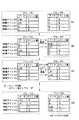
また、本発明の例では、上述したように、ページイレーズ機能に起因する電圧ストレスの問題に関しては、1つのブロック内のページのデータ書き換え回数を、ページごとに管理することにより解決する。このデータ書き換え回数は、図1に示すように、メモリセルアレイの冗長部に、ページごとに、カウント値として記憶される。
【0041】
本発明の例では、このカウント値が重要であり、冗長部に記憶される他のデータ、即ち、論理アドレス、ブロックの良否を示すフラグ(ブロックステータス)、ECC符号などは、従来と同じである。そこで、以下に説明する実施の形態では、冗長部については、説明の簡単化のため、データ書き換え回数、即ち、カウント値のみを示すことにする。
【0042】
また、NAND型フラッシュメモリの説明において、ライト動作時に、非選択のページのメモリセルに電圧ストレスが印加されることを説明した。ここで、セルデータが破壊されることなく、この電圧ストレスにメモリセルが耐え得る回数、即ち、非選択のページ内のメモリセルが経験し得るデータ書き換え回数(ライト/イレーズ回数)の最大値(許容値)を、32回と仮定する。
【0043】
4. 実施の形態1
以下、実施の形態1について説明する。
【0044】
この実施の形態の特徴は、ページイレーズ機能を有するNAND型フラッシュメモリにおいて、ページ単位で、データ書き換え回数を管理し、1つのブロック内の各ページのデータ書き換え回数が所定の条件を満たしたときに、その1つのブロックについてリフレッシュ動作を行う、という点にある。
【0045】
ここで、データ書き換えは、1つ又は複数のページ単位で行ってもよく、また、ブロック単位で行ってもよい。重要な点は、データ書き換えを行う度に、データ書き換えを実行したページに対して、ページごとに、データ書き換え回数をカウントすることにある。なお、後述するが、カウント方法は、特に、限定されない。
【0046】
また、ここで言う「リフレッシュ動作」とは、1つのブロック内の特定のページ(全ページ又は1つ以上のページ)に対して、データの再書き込み(rewrite)を行うことである。リフレッシュ動作の意味又は目的は、非選択ページのデータが電圧ストレスにより破壊される前に、その非選択ページのデータをリフレッシュするという点にあり、意味的又は目的的には、DRAMのリフレッシュ動作と同じである。なお、リフレッシュ動作の方法についても、後述するように、特に、限定されない。
【0047】
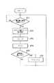
図2は、本発明の実施の形態1に関わるシステムを示している。図3は、本発明の実施の形態1に関わるシステムの動作の主要部を示している。
【0048】
メモリ10とは、例えば、ページイレーズ機能を有するNANDフラッシュメモリのことである。コントローラ11とは、メモリ10の動作をコントロールし、かつ、ページごとのデータ書き換え回数を管理するコントロール回路のことである。
【0049】
メモリ10とコントローラ11は、1チップ化されていてもよいし、それぞれ別のチップに形成されていてもよい。また、両者は、メモリカードのような1つの機器内に配置されていてもよいし、メモリカードと電子機器のように、別の機器内に配置されていてもよい。
【0050】
まず、メモリ10は、コントローラ11からの書き換え信号を受けると、データ書き換えを行うページを含む選択されたブロック内の全ページのカウント値のリードを実行する(ステップST1〜ST2)。
【0051】
コントローラ11は、選択されたブロック内の全ページのうち、データ書き換えを実行するページに対して、カウント値の更新を行う。ここでは、カウント方法に応じて、カウントの仕方が異なるため、カウント値の更新という言葉を使用している(ステップST2)。
【0052】
この後、データイレーズ及びデータライトを実行する(ステップST3〜ST4)。
【0053】
データイレーズは、ページ単位でイレーズを実行するページイレーズでもよいし、ブロック単位又はチップ単位でイレーズを実行するブロックイレーズ又はチップイレーズでもよい。要は、メモリ10が、ページ単位でイレーズするページイレーズ機能を有していればよい。
【0054】
データライトは、ページ単位で実行される。選択されたブロック内の複数又は全てのページに対するデータ書き換えを実行する場合には、例えば、ソース線に近いメモリセルから順に、1ページずつ、データライトを実行する。データライトでは、新たなデータがデータ領域に記憶されると共に、新たなカウント値が冗長部に記憶される。
【0055】
次に、コントローラ11は、選択されたブロック内の各ページのカウント値に基づいて、データ書き換え回数が最大値(許容値)に達したか否かを判断する(ステップST5)。
【0056】
データ書き換え回数が最大値(許容値)に達していない場合には、本発明に関わる動作としては、特に、何も行わない。即ち、メモリ10は、コントローラ11のコントロールの下で、通常の動作を行う。
【0057】
データ書き換え回数が最大値(許容値)に達している場合には、コントローラ11は、メモリ10に対して、リフレッシュ動作を行う命令を出す。リフレッシュ動作の方法については、後に詳述する。リフレッシュ動作を行ったら、原則として、その選択されたブロック内の各ページのデータ書き換え回数(カウント値)を初期化する。但し、カウント方法によっては、データ書き換え回数を初期化しなくてもよい場合がある(ステップST6)。
【0058】
5. 実施の形態2
以下、実施の形態2について説明する。
【0059】
この実施の形態は、実施の形態1の変形例である。この実施の形態では、実施の形態1における言葉の定義及びその他の条件がそのまま適用される。
【0060】
実施の形態1では、データ書き換え回数が所定の条件を満たしたときにリフレッシュ動作を行った。
【0061】
しかし、この場合、最後のデータ書き換えの対象となるページについては、データ書き換え(イレーズ及びライト)を実行した後に、連続して、リフレッシュ動作(イレーズ及びライト)が実行されることになる。つまり、最後のデータ書き換え動作は、冗長となる。
【0062】
そこで、この実施の形態では、最後のデータ書き換えの対象となるページに対してのデータ書き換え動作については、リフレッシュ動作の中で行うようにする。このようにすれば、無駄なデータ書き換え動作をなくすことができ、データ書き換え性能の向上を図ることができる。
【0063】
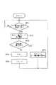
図2は、本発明の実施の形態2に関わるシステムを示している。図4は、本発明の実施の形態2に関わるシステムの動作の主要部を示している。
【0064】
メモリ10及びコントローラ11については、既に、上述の実施の形態1で説明したため、ここでは、省略する。
【0065】
まず、メモリ10は、コントローラ11からの書き換え信号を受けると、データ書き換えを行うページを含む選択されたブロック内の全ページのカウント値のリードを実行する(ステップST1〜ST2)。
【0066】
コントローラ11は、選択されたブロック内の全ページのうち、データ書き換えを実行するページに対して、カウント値の更新を行う。カウント値の更新という言葉は、上述したように、カウント方法に応じてカウントの仕方が異なるために使用したものである(ステップST2)。
【0067】
次に、コントローラ11は、選択されたブロック内の各ページのカウント値に基づいて、データ書き換え回数が最大値(許容値)に達したか否かを判断する(ステップST3)。
【0068】
データ書き換え回数が最大値(許容値)に達していない場合には、データイレーズ及びデータライトを実行する(ステップST4〜ST5)。
【0069】
データイレーズは、ページ単位でイレーズを実行するページイレーズでもよいし、ブロック単位又はチップ単位でイレーズを実行するブロックイレーズ又はチップイレーズでもよい。
【0070】
データライトは、ページ単位で実行される。選択されたブロック内の複数又は全てのページに対するデータ書き換えを実行する場合には、例えば、ソース線に近いメモリセルから順に、1ページずつ、データライトを実行する。データライトでは、新たなデータがデータ領域に記憶されると共に、新たなカウント値が冗長部に記憶される。
【0071】
データ書き換え回数が最大値(許容値)に達している場合には、コントローラ11は、メモリ10に対して、リフレッシュ動作を行う命令を出す(ステップST6)。
【0072】
リフレッシュ動作の方法については、後に詳述するが、実施の形態2では、少なくとも、選択されたブロック内のデータ書き換えの対象となるページについては、このリフレッシュ動作によってデータ書き換えを実行する。また、選択されたブロック内のデータ書き換えの対象とならないページについては、通常のリフレッシュ動作が実行される。
【0073】
リフレッシュ動作を行ったら、原則として、その選択されたブロック内の各ページのデータ書き換え回数(カウント値)を初期化する。但し、カウント方法によっては、データ書き換え回数を初期化しなくてもよい場合がある。
【0074】
6. 実施の形態1,2に関する実施例
以下、実施の形態1,2に関する実施例について説明する。
【0075】
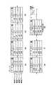
(1) 実施例1
▲1▼ カウント方法
図5は、本発明の実施例1に関わるカウント方法を示している。
【0076】
本例では、カウント値は、NAND型フラッシュメモリのメモリセルアレイ内の冗長部に記憶される。カウント値は、ページに対するデータ書き換え回数を表しており、ページごとに記憶される。
【0077】
リフレッシュの実施は、ブロック内の各ページのカウント値の合計が、最大値(許容値)、32回に達したことを条件とする。即ち、データ書き換え動作に関し、最悪のケースとしては、少なくとも1つのページが一度も選択されない場合が考えられる。この選択されないページ内のメモリセルについては、32回までのデータ書き換えに起因する電圧ストレスに耐え得ることから、上述のような条件を設定する。
【0078】
なお、実施例1の説明において、物理アドレス0,1,2,3とは、アドレス信号0,1,2,3により選択されるメモリセル、即ち、ページ0,1,2,3のことである。
【0079】
物理アドレス0,1,2,3なる言葉を採用した理由は、1本のワード線に接続される複数のメモリセル(1物理アドレス)の各々が1ビットデータを記憶する場合には、1ページは、1物理アドレスに等しくなるが、複数ビットを記憶する場合(多値メモリの場合)には、1ページは、1物理アドレスに等しくならないことを考慮したものである。
【0080】
論理アドレス0,1,2,3とは、アドレス信号0,1,2,3のことである。
【0081】
また、例えば、物理アドレス0に記憶されるデータは、物理アドレス0が論理アドレス0により選択されるということから、「LA0」と記載する。なお、各メモリセルに記憶されるデータは、1ビットであるか、又は、多ビットであるかを問わない。同様の理由により、物理アドレス1,2,3に記憶されるデータは、「LA1」、「LA2」、「LA3」と記載する。「E」は、メモリセルがイレーズ状態にあることを示している。
【0082】
(a) 初期状態
ブロック内の全ての物理アドレス(ページ)0,1,2,3内のメモリセルは、イレーズ状態にある。
【0083】
(b) ライト
まず、物理アドレス0にデータLA0がライトされ、物理アドレス1にデータLA1がライトされ、物理アドレス2にデータLA2がライトされ、物理アドレス3にデータLA3がライトされる。
【0084】
物理アドレス0に対するデータLA0のライト時には、物理アドレス0のカウント値、即ち、データ書き換え回数として、“1”が冗長部にライトされる。同様に、物理アドレス1,2,3に対するデータLA1,2,3のライト時には、物理アドレス1,2,3のカウント値、即ち、データ書き換え回数として、“1”が冗長部にライトされる。
【0085】
(c) 及び(d) 物理アドレス0のデータ書き換え
コントローラ11は、メモリ10に対して、物理アドレス0のデータ更新要求を出力する(図2参照)。
【0086】
まず、ブロック内の全ての物理アドレス0,1,2,3のカウント値がリードされる。また、図2のコントローラ11において、データ書き換えの対象となる物理アドレス0のカウント値に、“1”が加算される。その結果、物理アドレス0のカウント値は、“2”になる。物理アドレス0,1,2,3のカウント値は、例えば、図2のコントローラ11内のメモリ(RAMなど)に一時的に記憶される。
【0087】
この後、物理アドレス0に記憶されたデータLA0及びカウント値のイレーズが実行される((c)参照)。続けて、物理アドレス0に対して、更新データLA0及びカウント値(=“2”)がライトされる((d)参照)。
【0088】
また、図2のコントローラ11において、全ての物理アドレス0,1,2,3のカウント値の合計値が算出される。この時点では、物理アドレス0のカウント値は、“2”であり、また、物理アドレス1,2,3のカウント値は、“1”であるため、全ての物理アドレス0,1,2,3のカウント値の合計値は、“5”となる。この合計値は、最大値(許容値)、“32”よりも小さい。
【0089】
従って、この時点では、リフレッシュ動作は、行われない。
【0090】
(e) 及び(f) 物理アドレス2のデータ書き換え
コントローラ11は、メモリ10に対して、物理アドレス2のデータ更新要求を出力する(図2参照)。
【0091】
ブロック内の全ての物理アドレス0,1,2,3のカウント値がリードされる。また、図2のコントローラ11において、データ書き換えの対象となる物理アドレス2のカウント値に、“1”が加算される。その結果、物理アドレス2のカウント値は、“2”になる。物理アドレス0,1,2,3のカウント値は、例えば、図2のコントローラ11内のメモリ(RAMなど)に一時的に記憶される。
【0092】
この後、物理アドレス2に記憶されたデータLA2及びカウント値のイレーズが実行される((e)参照)。続けて、物理アドレス2に対して、更新データLA2及びカウント値(=“2”)がライトされる((f)参照)。
【0093】
また、図2のコントローラ11において、全ての物理アドレス0,1,2,3のカウント値の合計値が算出される。この時点では、物理アドレス0,2のカウント値は、“2”であり、また、物理アドレス1,3のカウント値は、“1”であるため、全ての物理アドレス0,1,2,3のカウント値の合計値は、“6”となる。この合計値は、最大値(許容値)、“32”よりも小さい。
【0094】
従って、この時点でも、リフレッシュ動作は、行われない。
【0095】
(g) リフレッシュ
データ更新要求に従い、上述の(c)及び(d)の動作又は(e)及び(f)の動作と同様の動作が実行され、最終的に、物理アドレス0,1,2,3のカウント値が、(g) に示すようになったとする。
【0096】
図2のコントローラ11は、物理アドレス0,1,2,3のカウント値の合計値が“32”であることを確認すると、リフレッシュ動作を行う命令を、図2のメモリ10に与える。
【0097】
本例の場合、物理アドレス0,1,2,3のカウント値は、全て、“1”以上となっている。即ち、物理アドレス0,1,2,3のいずれに関しても、32回のデータ書き換え動作のうち、少なくとも1回は、データ書き換えの対象となっている。従って、データ書き換えの対象とならない状態で32回の電圧ストレスを受けた物理アドレスは、存在しない。
【0098】
しかし、上述したように、最悪のケースとしては、32回のデータ書き換え動作において、少なくとも1つの物理アドレスが、一度も選択されない場合が考えられる。この場合、その少なくとも1つの物理アドレスについては、データ書き換えの対象とならない状態で32回の電圧ストレスを受けたことになる。
【0099】
そこで、物理アドレス0,1,2,3のカウント値の合計値が、最大値(許容値)、“32”に達したときは、各物理アドレス0,1,2,3のカウント値に関係なく、リフレッシュ動作を実行する。
【0100】
なお、本例では、初期状態で全ての物理アドレス0,1,2,3がイレーズ状態で、かつ、最初の1回目は、全ての物理アドレス0,1,2,3に対するデータライト動作となっている。従って、最悪のケースとしては、正確には、2回目以降、一度もデータ書き換えの対象とならないケースとなる。
【0101】
つまり、メモリセルのデータ破壊が32回の電圧ストレスまで発生しないとすると、リフレッシュの条件は、物理アドレス0,1,2,3のカウント値の合計値が“33”に達したこと、となる。
【0102】
本例では、リフレッシュの条件は、物理アドレス0,1,2,3のカウント値の合計値に基づいているが、この条件は、メモリの初期状態に応じて変更される。重要な点は、最悪のケースを想定し、この最悪のケースに基づいて、最大値(許容値)を決定することにある。
【0103】
リフレッシュ動作では、データ領域に記憶されるデータについては、再書き込みによりリフレッシュされるが、冗長部のカウント値については、リフレッシュ動作時に、例えば、(b) の状態に初期化される。即ち、リフレッシュにおけるライト動作では、物理アドレス0,1,2,3に対応する冗長部に、それぞれ、カウント値“1”がライトされる。
【0104】
▲2▼ リフレッシュ動作の方法
リフレッシュ動作の方法について説明する。
【0105】
リフレッシュとは、上述のように、ブロック内の全ページ又は1つ以上のページに対して、データの再書き込み(rewrite)を行うことである。リフレッシュの目的は、メモリセルのデータが電圧ストレスによる閾値変動により破壊される前に、そのメモリセルのデータをリフレッシュするという点にあり、この目的が実現できれば、どのような方法を用いてもよい。
【0106】
(a) リフレッシュの例1
例えば、リフレッシュを行うブロック内の全ての物理アドレスのデータを、コントローラ内のメモリ(RAMなど)に転送した後、そのブロック内の全ての物理アドレスのデータをイレーズする。このイレーズは、ブロックイレーズでもよく、また、ページイレーズでもよい。そして、コントローラ内のメモリに一時的に記憶されたデータを、再び、そのブロック内の物理アドレスに戻す。これにより、リフレッシュの対象となった物理アドレスを構成するメモリセルのデータがリフレッシュされる。
【0107】
(b) リフレッシュの例2
まず、リフレッシュを行う一のブロック内の全ての物理アドレスのデータを、リフレッシュを行わない他のブロックに転送した後、その一のブロック内の全ての物理アドレスのデータをイレーズする。このイレーズは、ブロックイレーズでもよく、また、ページイレーズでもよい。そして、他のブロックに一時的に記憶されたデータを、再び、一のブロック内の物理アドレスに戻す。これにより、リフレッシュの対象となった物理アドレスを構成するメモリセルのデータがリフレッシュされる。この例では、一のブロックと他のブロックは、同一チップ内に形成されていてもよいし、それぞれ異なるチップ内に形成されていてもよい。
【0108】
▲3▼ リフレッシュ動作のタイミング
リフレッシュ動作を実施するタイミングは、特に、限定されない。
【0109】
例えば、許容値が“32”の場合、ブロック内の物理アドレスのカウント値の合計値が32回に達し、かつ、32回目の書き換え動作を終えたなら、その後、直ちに、リフレッシュ動作を実行してもよい。また、32回目の書き換え動作を終えた後の適当な時期、例えば、ホストからのアクセスが途絶えた後に、リフレッシュ動作を実行してもよい。
【0110】
なお、実施の形態2に基づく実施例の場合には、32回目のデータ書き換え動作をリフレッシュ動作の中で行っている。このため、リフレッシュ動作は、ブロック内の物理アドレスのカウント値の合計値が32回に達した後、32回目の書き換え動作と共に、直ちに、実行される。
【0111】
▲4▼ その他
本例では、カウント値は、0,1,2,・・・という具合に、“0”から始まり、データ更新回数に応じて“1”ずつ増えていくが、本発明の例は、このような数え方に限定されるものではない。
【0112】
例えば、初期値は、“0”以外の数値、例えば、“2”、二進数では“10”であってもよいし、増加分は、“1”ではなく、他の数値、例えば、“2”であってもよい。この場合、データ書き換え回数の最大値(許容値)も、当然に変わる。本例では、カウント値は、“32”が最大となるため、メモリセルアレイの冗長部としては、“32”までの数をカウントできるだけのビット数を確保しておけば、足りる。つまり、1つの物理アドレスに対しては、冗長部のうちの5ビットを、カウント値を記憶するための領域として使用する。
【0113】
また、カウント値の増加分は、等差数列的でなくてもよい。
【0114】
例えば、メモリセルアレイの冗長部のうち、4バイト、即ち、32ビット分を、カウント値を記憶する領域として使用する場合には、データ書き換え回数は、これら32ビットのうち、“1”状態にあるビットの数により判断してもよい。
【0115】
具体的には、所定の物理アドレスに対応するカウント値の初期値は、“00000・・・000(32ビット)”に設定しておき、データ更新回数に応じて、この領域における“1”の数を増やしていく。例えば、データ更新回数が1回の場合には、“00000・・・001”(32ビットのうち“1”の数は1個)となり、データ更新回数が2回の場合には、“00000・・・011”(32ビットのうち“1”の数は2個)となる。
【0116】
また、例えば、メモリセルアレイの冗長部のうち、4バイト、即ち、32ビット分を、カウント値を記憶する領域として使用する場合には、データ書き換え回数は、これら32ビットのうち、“1”状態にあるビットの位置により判断してもよい。
【0117】
具体的には、所定の物理アドレスに対応するカウント値の初期値は、“00000・・・000(32ビット)”に設定しておき、データ更新回数に応じて、この領域における“1”の位置を変えていく。例えば、データ更新回数が1回の場合には、“00000・・・001”(32ビットのうち“1”の位置は右端部)となる。データ更新回数が増えるに従い、“1”の位置を、1つずつ左にシフトさせる。
【0118】
また、カウント値は、データ更新回数に応じて増加させるのではなく、減少させるようにしてもよい。例えば、カウント値の初期値を“32”として、データ更新回数に応じて、この数を、1ずつ、減らしていってもよい。
【0119】
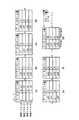
(2) 実施例2
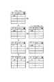
▲1▼ カウント方法
図6は、本発明の実施例2に関わるカウント方法を示している。
【0120】
上述の実施例1では、ページごとにデータ書き換え回数を管理し、コントローラは、データ書き換えの度に、ページごとのデータ書き換え回数に基づいて、ブロック内のデータ書き換え回数の合計値を算出した。
【0121】
これに対し、実施例2では、ブロック内におけるデータ書き換え回数の合計値を管理する。つまり、データ書き換えの対象となったページのカウント値は、そのページに対するデータ書き換え回数ではなく、そのページを含むブロック内におけるデータ書き換え回数の合計値に設定される。
【0122】
従って、コントローラは、データ書き換えの度に、ブロック内の各ページのカウント値のうちから最大値Nmaxであるものを選択すればよい。
【0123】
そして、リフレッシュの実施は、ブロック内の各ページのカウント値のうちの最大値Nmaxが、許容値、32回に達したことを条件とする。なぜなら、データ書き換え動作に関し、最悪のケースとしては、少なくとも1つのページが一度も選択されない場合が考えられるからである。この選択されないページ内のメモリセルについては、32回までのデータ書き換えに起因する電圧ストレスに耐え得ることから、上述のような条件を設定する。
【0124】
なお、実施例2の説明においても、物理アドレス0,1,2,3及び論理アドレス0,1,2,3の意味は、実施例1と同じであるため、ここでは、その説明を省略する。また、LA0、LA1、LA2、LA3及びEの意味についても、実施例1と同じであるため、ここでは、省略する。
【0125】
(a) 初期状態
ブロック内の全ての物理アドレス(ページ)0,1,2,3内のメモリセルは、イレーズ状態にある。
【0126】
(b) ライト
まず、物理アドレス0にデータLA0がライトされ、物理アドレス1にデータLA1がライトされ、物理アドレス2にデータLA2がライトされ、物理アドレス3にデータLA3がライトされる。
【0127】
物理アドレス0に対するデータLA0のライト時には、物理アドレス0のカウント値、即ち、データ書き換え回数として、“1”がライトされる。また、物理アドレス1に対するデータLA1のライト時には、ブロック全体としてみると、2回目のデータ書き換えであるため、物理アドレス1のカウント値、即ち、データ書き換え回数としては、“2”がライトされる。
【0128】
同様に、物理アドレス2に対するデータLA2のライト時には、ブロック全体としてみると、3回目のデータ書き換えであるため、物理アドレス2のカウント値、即ち、データ書き換え回数としては、“3”がライトされる。また、物理アドレス3に対するデータLA3のライト時には、ブロック全体としてみると、4回目のデータ書き換えであるため、物理アドレス3のカウント値、即ち、データ書き換え回数としては、“4”がライトされる。
【0129】
(c) 及び(d) 物理アドレス0のデータ書き換え
コントローラ11は、メモリ10に対して、物理アドレス0のデータ更新要求を出力する(図2参照)。
【0130】
まず、ブロック内の全ての物理アドレス0,1,2,3のカウント値がリードされる。図2のコントローラ11は、物理アドレス0,1,2,3のカウント値のうちから最大値Nmaxを選択する。この時点では、物理アドレス3のカウント値“4”が最も大きな値を有する。図2のコントローラ11は、物理アドレス3のカウント値“4”に“1”を加算し、カウント値“5”を、データ書き換えの対象となる物理アドレス0のカウント値とする。物理アドレス0,1,2,3のカウント値は、例えば、図2のコントローラ11内のメモリ(RAMなど)に一時的に記憶される。
【0131】
この後、物理アドレス0に記憶されたデータLA0及びカウント値のイレーズが実行される((c)参照)。続けて、物理アドレス0に対して、更新データLA0及びカウント値(=“5”)がライトされる((d)参照)。
【0132】
また、図2のコントローラ11は、物理アドレス0,1,2,3のカウント値のうちの最大値Nmaxが、許容値、“32”に達しているか否かを判断する。この時点では、物理アドレス0のカウント値“5”が最も大きいが、その値は、許容値、“32”に達していない。
【0133】
従って、この時点では、リフレッシュ動作は、行われない。
【0134】
(e) 及び(f) 物理アドレス2のデータ書き換え
コントローラ11は、メモリ10に対して、物理アドレス2のデータ更新要求を出力する(図2参照)。
【0135】
まず、ブロック内の全ての物理アドレス0,1,2,3のカウント値がリードされる。図2のコントローラ11は、物理アドレス0,1,2,3のカウント値のうちから最大値Nmaxを選択する。この時点では、物理アドレス0のカウント値“5”が最も大きな値を有する。図2のコントローラ11は、物理アドレス0のカウント値“5”に“1”を加算し、カウント値“6”を、データ書き換えの対象となる物理アドレス2のカウント値とする。物理アドレス0,1,2,3のカウント値は、例えば、図2のコントローラ11内のメモリ(RAMなど)に一時的に記憶される。
【0136】
この後、物理アドレス2に記憶されたデータLA2及びカウント値のイレーズが実行される((e)参照)。続けて、物理アドレス2に対して、更新データLA2及びカウント値(=“6”)がライトされる((f)参照)。
【0137】
また、図2のコントローラ11は、物理アドレス0,1,2,3のカウント値のうちの最大値Nmaxが、許容値、“32”に達しているか否かを判断する。この時点では、物理アドレス2のカウント値“6”が最も大きいが、その値は、許容値、“32”に達していない。
【0138】
従って、この時点では、リフレッシュ動作は、行われない。
【0139】
(g) リフレッシュ
データ更新要求に従い、上述の(c)及び(d)の動作又は(e)及び(f)の動作と同様の動作が実行され、最終的に、物理アドレス0,1,2,3のカウント値が、(g) に示すようになったとする。
【0140】
図2のコントローラ11は、物理アドレス0,1,2,3のカウント値の最大値Nmaxが“32”であることを確認すると、リフレッシュ動作を行う命令を、図2のメモリ10に与える。
【0141】
本例の場合、物理アドレス0,1,2,3のカウント値は、全て、“1”以上となっている。即ち、物理アドレス0,1,2,3のいずれに関しても、32回のデータ書き換え動作のうち、少なくとも1回は、データ書き換えの対象となっている。従って、データ書き換えの対象とならない状態で32回の電圧ストレスを受けた物理アドレスは、存在しない。
【0142】
しかし、上述したように、最悪のケースとしては、32回のデータ書き換え動作において、少なくとも1つの物理アドレスが、一度も選択されない場合が考えられる。この場合、その少なくとも1つの物理アドレスについては、データ書き換えの対象とならない状態で32回の電圧ストレスを受けたことになる。
【0143】
そこで、物理アドレス0,1,2,3のカウント値の最大値Nmaxが、許容値、“32”に達したときは、各物理アドレス0,1,2,3のカウント値に関係なく、リフレッシュ動作を実行する。
【0144】
なお、本例では、初期状態で全ての物理アドレス0,1,2,3がイレーズ状態で、かつ、最初の1回目は、全ての物理アドレス0,1,2,3に対するデータライト動作となっている。従って、最悪のケースとしては、正確には、2回目以降、一度もデータ書き換えの対象とならないケースとなる。
【0145】
つまり、メモリセルのデータ破壊が32回の電圧ストレスまで発生しないとすると、リフレッシュの条件は、物理アドレス0,1,2,3のカウント値の最大値Nmaxが“33”に達したこと、となる。
【0146】
本例では、リフレッシュの条件は、物理アドレス0,1,2,3のカウント値の最大値Nmaxに基づいているが、この条件は、メモリの初期状態に応じて変更される。重要な点は、最悪のケースを想定し、この最悪のケースに基づいて、許容値を決定することにある。
【0147】
リフレッシュ動作では、データ領域に記憶されるデータについては、再書き込みによりリフレッシュされるが、冗長部のカウント値については、リフレッシュ動作時に、例えば、(b) の状態に初期化される。即ち、リフレッシュにおけるライト動作では、物理アドレス0,1,2,3に対応する冗長部に、それぞれ、カウント値“1”,“2”,“3”,“4”がライトされる。
【0148】
▲2▼ リフレッシュ動作の方法
リフレッシュ動作は、メモリセルのデータが電圧ストレスによる閾値変動により破壊される前に、そのメモリセルのデータをリフレッシュするという目的が達成できれば、どのような方法を用いてもよい。例えば、リフレッシュ動作の方法としては、実施例1で説明した例1及び例2を、そのまま使用できるため、その詳細な説明については、省略する。
【0149】
▲3▼ リフレッシュ動作のタイミング
リフレッシュ動作を実施するタイミングは、特に、限定されない。
【0150】
例えば、許容値が“32”の場合、ブロック内の物理アドレスのカウント値の最大値Nmaxが32回に達し、かつ、32回目の書き換え動作を終えたなら、その後、直ちに、リフレッシュ動作を実行してもよい。また、32回目の書き換え動作を終えた後の適当な時期、例えば、ホストからのアクセスが途絶えた後に、リフレッシュ動作を実行してもよい。
【0151】
なお、実施の形態2に基づく実施例の場合には、32回目のデータ書き換え動作をリフレッシュ動作の中で行っている。このため、リフレッシュ動作は、ブロック内の物理アドレスのカウント値の最大値Nmaxが32回に達した後、32回目の書き換え動作と共に、直ちに、実行される。
【0152】
▲4▼ その他
本例では、カウント値は、0,1,2,・・・という具合に、“0”から始まり、ブロック内におけるデータ書き換え回数に応じて“1”ずつ増えていくが、本発明の例は、このような数え方に限定されるものではない。
【0153】
例えば、実施例1と同様に、初期値は、“0”以外の数値、例えば、“2”、二進数では“10”であってもよいし、増加分は、“1”ではなく、他の数値、例えば、“2”であってもよい。この場合、ブロック内のデータ書き換え回数の許容値も、当然に変わる。
【0154】
本例では、カウント値は、“32”よりも大きくなることはないため、メモリセルアレイの冗長部としては、“32”までの数をカウントできるだけのビット数を確保しておけば、足りる。つまり、メモリセルアレイの冗長部のうちの5ビットを、カウント値を記憶するための領域として使用すればよい。
【0155】
また、カウント値の増加分は、等差数列的でなくてもよい。実施例1で説明したように、例えば、メモリセルアレイの冗長部のうち、4バイト、即ち、32ビット分を、カウント値を記憶する領域として使用し、データ書き換え回数については、これら32ビットのうち、“1”状態にあるビットの数により判断してもよい。また、例えば、データ書き換え回数については、これら32ビットのうち、“1”状態にあるビットの位置により判断してもよい。
【0156】
また、カウント値は、データ更新回数に応じて増加させるのではなく、減少させるようにしてもよい。例えば、カウント値の初期値を“32”として、データ更新回数に応じて、この数を、1ずつ、減らしていってもよい。
【0157】
(3) 実施例3
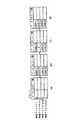
▲1▼ カウント方法
図7は、本発明の実施例3に関わるカウント方法を示している。
【0158】
上述の実施例1及び実施例2においては、最悪条件を仮定し、ブロック内におけるデータ書き換え回数の合計値が許容値、例えば、32回に達した時点でリフレッシュ動作を実行する手法を採用した。この場合、ブロック内におけるデータ書き換え回数の合計値が許容値に達すると、各ページにおけるデータ書き換え回数にかかわらず、常に、リフレッシュ動作が行われる。
【0159】
これは、反面、リフレッシュ動作を行う必要がない場合、例えば、ブロック内の各ページが短い周期(32回未満)でデータ書き換えの対象となる場合であっても、ブロック内のデータ書き換え回数が許容値に達すると、必然的にリフレッシュ動作を行うことを意味している。つまり、無駄なリフレッシュ動作が行われる可能性がある。
【0160】
実施例3では、このような無駄なリフレッシュ動作を完全に排除するための手法を提案する。
【0161】
カウント方法に関しては、実施例3は、実施例2と同じである。即ち、データ書き換えの対象となったページのカウント値は、そのページに対するデータ書き換え回数ではなく、そのページを含むブロック内におけるデータ書き換え回数の合計値に設定される。
【0162】
しかし、実施例3では、リフレッシュの発生条件が実施例2と異なる。
【0163】
実施例2では、コントローラは、データ書き換えの度に、ブロック内の各ページのカウント値のうちから最大値Nmaxであるものを選択し、その最大値Nmaxが許容値、例えば、32回に達しているか否かを判断した。これに対し、実施例3では、コントローラは、データ書き換えの度に、ブロック内の各ページのカウント値のうちから最大値Nmaxと最小値Nminとを選択し、その最大値Nmaxと最小値Nminとの差が許容値、例えば、32回に達しているか否かを判断する。
【0164】
ここで、カウント値が最大値Nmaxであるということは、そのカウント値に対応するページのデータ更新が、現在に対して最も近い時期に行われたことを意味する。また、カウント値が最小値Nminであるということは、そのカウント値に対応するページのデータ更新が、現在に対して最も遠い時期に行われたことを意味する。
【0165】
そして、最大値Nmaxと最小値Nminとの差は、カウント値が最小値Nminであるページのデータ更新が最後に行われた後のブロック内のデータ書き換え回数を意味する。つまり、カウント値が最小値Nminであるページ内のメモリセルは、そのページのデータ更新が最後に行われた後、最大値Nmaxと最小値Nminとの差に相当する回数の電圧ストレスを受けたことになる。
【0166】
このように、実施例3では、ブロック内の各ページのカウント値のうち最大値Nmaxと最小値Nminを抽出し、その差分をもって、リフレッシュ動作の必要性を判断している。
【0167】
実施例3の利点は、最大値Nmaxと最小値Nminの差分が許容値未満であれば、リフレッシュ動作を実行することなく、データ書き換え動作を継続して行うことができるという点にある。つまり、実施例3は、無駄なリフレッシュ動作を省くことで、実施例1及び実施例2に比べ、リフレッシュ動作の回数を大幅に減らすことができる。
【0168】
なお、実施例3の説明においても、物理アドレス0,1,2,3及び論理アドレス0,1,2,3の意味は、実施例1と同じであるため、ここでは、その説明を省略する。また、LA0、LA1、LA2、LA3及びEの意味についても、実施例1と同じであるため、ここでは、省略する。
【0169】
(a) 初期状態
ブロック内の全ての物理アドレス(ページ)0,1,2,3内のメモリセルは、イレーズ状態にある。
【0170】
(b) ライト
まず、物理アドレス0にデータLA0がライトされ、物理アドレス1にデータLA1がライトされ、物理アドレス2にデータLA2がライトされ、物理アドレス3にデータLA3がライトされる。
【0171】
物理アドレス0に対するデータLA0のライト時には、物理アドレス0のカウント値、即ち、データ書き換え回数として、“1”がライトされる。また、物理アドレス1に対するデータLA1のライト時には、ブロック全体としてみると、2回目のデータ書き換えであるため、物理アドレス1のカウント値、即ち、データ書き換え回数としては、“2”がライトされる。
【0172】
同様に、物理アドレス2に対するデータLA2のライト時には、ブロック全体としてみると、3回目のデータ書き換えであるため、物理アドレス2のカウント値、即ち、データ書き換え回数としては、“3”がライトされる。また、物理アドレス3に対するデータLA3のライト時には、ブロック全体としてみると、4回目のデータ書き換えであるため、物理アドレス3のカウント値、即ち、データ書き換え回数としては、“4”がライトされる。
【0173】
(c) 及び(d) 物理アドレス0のデータ書き換え
コントローラ11は、メモリ10に対して、物理アドレス0のデータ更新要求を出力する(図2参照)。
【0174】
まず、ブロック内の全ての物理アドレス0,1,2,3のカウント値がリードされる。図2のコントローラ11は、物理アドレス0,1,2,3のカウント値のうちから最大値Nmaxを選択する。この時点では、物理アドレス3のカウント値“4”が最も大きな値を有する。図2のコントローラ11は、物理アドレス3のカウント値“4”に“1”を加算し、カウント値“5”を、データ書き換えの対象となる物理アドレス0のカウント値とする。物理アドレス0,1,2,3のカウント値は、例えば、図2のコントローラ11内のメモリ(RAMなど)に一時的に記憶される。
【0175】
この後、物理アドレス0に記憶されたデータLA0及びカウント値のイレーズが実行される((c)参照)。続けて、物理アドレス0に対して、更新データLA0及びカウント値(=“5”)がライトされる((d)参照)。
【0176】
また、図2のコントローラ11は、物理アドレス0,1,2,3のカウント値のうちの最大値Nmaxと最小値Nminを抽出する。そして、この最大値Nmaxと最小値Nminとの差を計算し、この差が、データ書き換え回数の最大値(許容値)、即ち、“32”に達しているか否かを判断する。
【0177】
この時点では、物理アドレス0のカウント値“5”が最も大きく、物理アドレス1のカウント値“2”が最も小さい。従って、最大値Nmax−最小値Nminは、“3”であり、この数値は、“32”よりも小さい。
【0178】
従って、この時点では、リフレッシュ動作は、行われない。
【0179】
(e) 及び(f) 物理アドレス2のデータ書き換え
コントローラ11は、メモリ10に対して、物理アドレス2のデータ更新要求を出力する(図2参照)。
【0180】
まず、ブロック内の全ての物理アドレス0,1,2,3のカウント値がリードされる。図2のコントローラ11は、物理アドレス0,1,2,3のカウント値のうちから最大値Nmaxを選択する。この時点では、物理アドレス0のカウント値“5”が最も大きな値を有する。図2のコントローラ11は、物理アドレス0のカウント値“5”に“1”を加算し、カウント値“6”を、データ書き換えの対象となる物理アドレス2のカウント値とする。物理アドレス0,1,2,3のカウント値は、例えば、図2のコントローラ11内のメモリ(RAMなど)に一時的に記憶される。
【0181】
この後、物理アドレス2に記憶されたデータLA2及びカウント値のイレーズが実行される((e)参照)。続けて、物理アドレス2に対して、更新データLA2及びカウント値(=“6”)がライトされる((f)参照)。
【0182】
また、図2のコントローラ11は、物理アドレス0,1,2,3のカウント値のうちの最大値Nmaxと最小値Nminを抽出する。そして、この最大値Nmaxと最小値Nminとの差を計算し、この差が、データ書き換え回数の最大値(許容値)、即ち、“32”に達しているか否かを判断する。
【0183】
この時点では、物理アドレス2のカウント値“6”が最も大きく、物理アドレス1のカウント値“2”が最も小さい。従って、最大値Nmax−最小値Nminは、“4”であり、この数値は、“32”よりも小さい。
【0184】
従って、この時点では、リフレッシュ動作は、行われない。
【0185】
(g) リフレッシュ
データ更新要求に従い、上述の(c)及び(d)の動作又は(e)及び(f)の動作と同様の動作が実行され、最終的に、物理アドレス0,1,2,3のカウント値が、(g) に示すようになったとする。
【0186】
図2のコントローラ11は、物理アドレス0,1,2,3のカウント値から最大値Nmaxと最小値Nminを抽出する。最大値Nmaxは、物理アドレス0のカウント値であり、その値は、“65”である。また、最小値Nminは、物理アドレス3のカウント値であり、その値は、“33”である。最大値Nmaxと最小値Nminとの差は、“32”となる。
【0187】
つまり、物理アドレス3のデータが最後に更新された後、物理アドレス3は、32(=65−33)回のデータ書き換えによる電圧ストレスを受けていることになる。従って、図2のコントローラ11は、この事実を確認すると、リフレッシュ動作を行う命令を、図2のメモリ10に与える。
【0188】
本例では、ブロック内の各物理アドレス0,1,2,3のカウント値の最大値Nmaxと最小値Nminの差に基づいて、リフレッシュ動作の必要性を判断している。このため、その差が許容値未満であれば、リフレッシュ動作を行う必要がない。場合によっては、リフレッシュ動作を全く行わずに、データ書き換え動作を継続して行うことができる。
【0189】
また、本例では、カウント値の最大値Nmaxと最小値Nminの差に基づいてリフレッシュ動作の必要性を判断しているため、実施例1,2のように、リフレッシュの条件がメモリの初期状態に依存することはない。また、本例では、実施例1,2のように、最悪のケースを想定して、リフレッシュの条件を設定しなくてもよい。
【0190】
リフレッシュ動作では、データ領域に記憶されるデータについては、再書き込みによりリフレッシュされるが、冗長部のカウント値については、リフレッシュ動作時に、例えば、(b) の状態に初期化される。即ち、リフレッシュにおけるライト動作では、物理アドレス0,1,2,3に対応する冗長部に、それぞれ、カウント値“1”,“2”,“3”,“4”がライトされる。
【0191】
なお、本例では、上述のリフレッシュ条件(Nmax−Nmin≧32)を満たしたときに、カウント値が最小値Nminである物理アドレスについてのみ、リフレッシュを行うようにしてもよい。この場合、リフレッシュ動作後には、リフレッシュの対象となった物理アドレスのカウント値のみを更新し、他のカウント値を初期化することなく、そのまま継続してカウントする。
【0192】
例えば、図7の例の場合には、(g) において、物理アドレスLA3のみについてリフレッシュを行い、このリフレッシュ動作によって、物理アドレスLA3のカウント値を“66”(=65+1)に設定してもよい。物理アドレスLA0,LA1,LA2のデータは、リフレッシュされないため、そのカウント値については、現状を維持させる。
【0193】
▲2▼ リフレッシュ動作の方法
リフレッシュ動作は、メモリセルのデータが電圧ストレスによる閾値変動により破壊される前に、そのメモリセルのデータをリフレッシュするという目的が達成できれば、どのような方法を用いてもよい。例えば、リフレッシュ動作の方法としては、実施例1で説明した例1及び例2を、そのまま使用できるため、その詳細な説明については、省略する。
【0194】
但し、本例では、上述したように、リフレッシュ動作は、ブロック内の全ての物理アドレスについて行ってもよく、また、ブロック内の物理アドレスのうち、カウント値が最小値Nminである物理アドレスのみについて行ってもよい。
【0195】
▲3▼ リフレッシュ動作のタイミング
リフレッシュ動作を実施するタイミングは、特に、限定されない。
【0196】
例えば、許容値が“32”の場合、ブロック内の物理アドレスのカウント値の最大値Nmaxと最小値Nminとの差が“32”に達したなら、データ書き換え動作を終えた後、直ちに、リフレッシュ動作を実行してもよい。また、データ書き換え動作を終えた後の適当な時期、例えば、ホストからのアクセスが途絶えた後に、リフレッシュ動作を実行してもよい。
【0197】
実施の形態2に基づく実施例の場合には、最大値Nmaxと最小値Nminとの差が“32”に達したときのデータ書き換え動作をリフレッシュ動作の中で行っている。このため、リフレッシュ動作は、ブロック内の物理アドレスのカウント値の最大値Nmaxと最小値Nminとの差が“32”に達したら、直ちに実行される。
【0198】
▲4▼ その他
本例では、カウント値は、0,1,2,・・・という具合に、“0”から始まり、ブロック内におけるデータ書き換え回数に応じて“1”ずつ増えていくが、本発明の例は、このような数え方に限定されるものではない。
【0199】
例えば、実施例1と同様に、初期値は、“0”以外の数値、例えば、“2”であってもよいし、増加分は、“1”ではなく、他の数値、例えば、“2”であってもよい。
【0200】
本例では、最大値Nmax−最小値Nminがリフレッシュ条件を満たさないと、カウント値は、限度なく、増加していく。しかし、カウント値を記憶するための冗長部のビット数には、限りがある。
【0201】
そこで、例えば、カウント値が、それを記憶するための冗長部のビット数により決まる上限値に到達したときは、上述のリフレッシュ条件にかかわらず、ブロック内の全ての物理アドレスについてリフレッシュを行い、かつ、全ての物理アドレスのカウント値を初期化してもよい。
【0202】
カウント値の増加分は、等差数列的でなくてもよい。実施例1で説明したように、例えば、メモリセルアレイの冗長部のうち、4バイト、即ち、32ビット分を、カウント値を記憶する領域として使用し、データ書き換え回数については、これら32ビットのうち、“1”状態にあるビットの数により判断してもよい。また、例えば、データ書き換え回数については、これら32ビットのうち、“1”状態にあるビットの位置により判断してもよい。
【0203】
また、カウント値は、データ更新回数に応じて増加させるのではなく、減少させるようにしてもよい。例えば、カウント値の初期値を、カウント値を記憶するための冗長部のビット数により決まる上限値として、データ更新回数に応じて、この数を、1ずつ、減らしていってもよい。
【0204】
7. 実施の形態3
以下、実施の形態3について説明する。
【0205】
実施の形態3は、データ更新中における電源の遮断(メモリカードで言えば、本体からの不意の抜き取りなどを含む)に対応できるシステムに関する。
【0206】
データ更新(データ書き換え)の方法としては、実施の形態1,2に関わる実施例1,2,3で説明したように、例えば、a. フラッシュメモリのブロック内の全ての物理アドレスのカウント値をコントローラ内の揮発性メモリ(RAMなど)に転送し、この後、b. データ更新の対象となる物理アドレスの古いデータ及び古いカウント値をイレーズし、この後、c. 新しいデータをデータ更新の対象となる物理アドレスに、新しいカウント値を冗長部に、それぞれ再書き込みする、という方法が採用される。
【0207】
この場合、b.のステップからc.のステップまでの間に電源の遮断が発生すると、データ更新の対象となる物理アドレスに関しては、古いデータ、新しいデータ、古いカウント値及び新しいカウント値の全てが消失してしまう。
【0208】
後述するが、本発明の例は、パソコンなどのファイル更新に適用される場合、比較的小さい容量で、かつ、高頻度でデータ更新が行われるFAT(File Allocation Table)情報の更新に対して有効になるものと思われる。しかし、本発明の例を適用したことにより、電源の遮断などに起因してデータが失われてしまうと、パソコンなどのシステムは、致命的な損傷を受けることになる。
【0209】
実施の形態3は、このような電源の遮断などにも対応できるように、実施の形態1を改良した改良例である。
【0210】
なお、以下の実施の形態3は、主として、データ更新方法についての説明となるが、リフレッシュ方法に適用することもできる。即ち、実施の形態3によれば、同様の原理により、リフレッシュ動作時の電源の遮断などに対応することができる。
【0211】
リフレッシュ動作の定義や意味などについては、実施の形態1と同じであるため、ここでは、省略する。
【0212】
図2は、本発明の実施の形態3に関わるシステムを示している。図8は、本発明の実施の形態3に関わるシステムの動作の主要部を示している。
【0213】
メモリ10及びコントローラ11については、既に、上述の実施の形態1で説明したため、ここでは、省略する。
【0214】
実施の形態3では、前提条件として、2つのメモリ領域(不揮発)をペアで使用する。各々のメモリ領域は、1つ以上のページを有する。また、2つのメモリ領域は、同じ数のページを有する。
【0215】
2つのメモリ領域は、共に、メモリ10の1つのブロック内に配置されていてもよい。また、2つのメモリ領域は、それぞれメモリ10の異なるブロック内に配置されていてもよい。さらに、2つのメモリ領域は、それぞれ異なるメモリ内に配置されていてもよい。
【0216】
まず、メモリ10は、コントローラ11からの書き換え信号を受けると、データ書き換えを行うページを含む2つのメモリ領域内の全ページのデータ及びカウント値のリードを実行する(ステップST1〜ST2)。
【0217】
コントローラ11は、データ書き換えを実行するページに対して、カウント値の更新を行う。ここで、実施の形態3が実施の形態1と異なる点は、この後、直ちに、データライトを実行し、その後に、データイレーズを実行する点にある(ステップST3〜ST4)。
【0218】
1つのメモリ領域内のページに対してデータ書き換えを実行する場合、データライトは、その1つのメモリ領域とペアとなっている他の1つのメモリ領域内のページに対して実行される。データライトでは、新たなデータがデータ領域に記憶されると共に、新たなカウント値が冗長部に記憶される。
【0219】
データライトの後に、データイレーズが行われる。
データイレーズは、1つのメモリ領域内のページに対して実行される。データイレーズは、ページ単位でイレーズを実行するページイレーズでもよいし、ブロック単位又はチップ単位でイレーズを実行するブロックイレーズ又はチップイレーズでもよい。
【0220】
次に、コントローラ11は、2つのメモリ領域内の各ページのカウント値に基づいて、データ書き換え回数が最大値(許容値)に達したか否かを判断する(ステップST5)。
【0221】
データ書き換え回数が最大値(許容値)に達していない場合には、本発明に関わる動作としては、特に、何も行わない。即ち、メモリ10は、コントローラ11のコントロールの下で、通常の動作を行う。
【0222】
データ書き換え回数が最大値(許容値)に達している場合には、コントローラ11は、メモリ10に対して、リフレッシュ動作を行う命令を出す。リフレッシュ動作を行ったら、原則として、2つのメモリ領域内の各ページのデータ書き換え回数(カウント値)を初期化する。但し、カウント方法によっては、データ書き換え回数を初期化しなくてもよい場合がある(ステップST6)。
【0223】
このように、実施の形態3では、2つのメモリ領域をペアで使用し、常に、新しいデータ及び新しいカウント値を2つのメモリ領域の一方にライトした後に、2つのメモリ領域の他方に記憶された古いデータ及び古いカウント値をイレーズするようにしている。このため、データ書き換え動作の最中に、電源の遮断などが発生しても、少なくとも、2つのメモリ領域のいずれか一方には、データ及びカウント値が保存されているため、システムとして致命的な損傷を受けることはない。
【0224】
8. 実施の形態4
以下、実施の形態4について説明する。この実施の形態は、実施の形態3の変形例である。リフレッシュ動作の定義や意味などについては、実施の形態1と同じであるため、ここでは、省略する。
【0225】
実施の形態3では、データ書き換え回数が所定の条件を満たしたときにリフレッシュ動作を行った。これに対し、実施の形態4では、カウント値が許容値に達する最後のデータ書き換え動作については、リフレッシュ動作の中で行うようにする。
【0226】
実施の形態3では、電源の不意の遮断などによるデータ消失を防止するため、2つのメモリ領域(不揮発)をペアで使用し、データ更新動作では、ライト動作を行った後にイレーズ動作を行うようにしている。しかし、リフレッシュ動作は、2つのメモリ領域に対して、同時に行うことになる。
【0227】
従って、実施の形態4では、カウント値が許容値に達する最後のデータ更新動作については、例えば、実施の形態2と同様の方法により、リフレッシュ動作(データ書き換え動作を含む)を実行する。
【0228】
但し、未使用のメモリ領域(不揮発)が存在すれば、リフレッシュ時に、その未使用のメモリ領域に、新しいデータ及び新しいカウント値をライトした後、2つのメモリ領域のデータ及びカウント値をイレーズしてもよい。
【0229】
図2は、本発明の実施の形態4に関わるシステムを示している。図9は、本発明の実施の形態4に関わるシステムの動作の主要部を示している。
【0230】
メモリ10及びコントローラ11については、既に、上述の実施の形態1で説明したため、ここでは、省略する。
【0231】
まず、メモリ10は、コントローラ11からの書き換え信号を受けると、データ書き換えを行うページを含む選択されたブロック内の全ページのデータ及びカウント値のリードを実行する(ステップST1〜ST2)。コントローラ11は、選択されたブロック内の全ページのうち、データ書き換えを実行するページに対して、データ書き換え回数の更新を行う(ステップST2)。
【0232】
次に、コントローラ11は、選択されたブロック内の各ページのカウント値に基づいて、データ書き換え回数が最大値(許容値)に達したか否かを判断する(ステップST3)。
【0233】
データ書き換え回数が最大値(許容値)に達していない場合には、データライト及びデータイレーズを実行する(ステップST4〜ST5)。
【0234】
1つのメモリ領域内のページに対してデータ書き換えを実行する場合、データライトは、その1つのメモリ領域とペアとなっている他の1つのメモリ領域内のページに対して実行される。データライトでは、新たなデータがデータ領域に記憶されると共に、新たなカウント値が冗長部に記憶される。
【0235】
データライトの後に、データイレーズが行われる。
データイレーズは、1つのメモリ領域内のページに対して実行される。データイレーズは、ページ単位でイレーズを実行するページイレーズでもよいし、ブロック単位又はチップ単位でイレーズを実行するブロックイレーズ又はチップイレーズでもよい。
【0236】
データ書き換え回数が最大値(許容値)に達している場合には、コントローラ11は、メモリ10に対して、リフレッシュ動作を行う命令を出す(ステップST6)。従って、ペアとなっている2つのメモリ領域内のデータがリフレッシュされると共に、データ書き換えの対象となるページについては、データ書き換えが実行される。
【0237】
リフレッシュ動作を行ったら、原則として、2つのメモリ領域内の各ページのデータ書き換え回数(カウント値)を初期化する。但し、カウント方法によっては、データ書き換え回数を初期化しなくてもよい場合がある。
【0238】
9. 実施の形態3,4に関する実施例
以下、実施の形態3,4に関する実施例について説明する。
【0239】
(1) 実施例1
▲1▼ データ更新方法
図10は、本発明の実施例1に関わるデータ更新方法を示している。
【0240】
なお、本例では、カウント方法として、実施の形態1,2に関する実施例2の方法が適用される。
【0241】
本例においては、1つのブロックは、4つの物理アドレスを有しているが、その1つのブロック内には、その半分、即ち、2つの物理アドレス(2ページ)分のデータのみを格納する。この点において、本例は、1つのブロック内の4つの物理アドレスに、4つの物理アドレス(4ページ)分のデータを格納する実施の形態1,2に関する実施例1,2,3とは異なる。
【0242】
物理アドレス0,1が1つのメモリ領域を構成し、物理アドレス2,3が他の1つのメモリ領域を構成する。これら2つのメモリ領域は、データ更新動作に関して、ペアを構成する。
【0243】
(a) 初期状態
ブロック内の全ての物理アドレス(ページ)0,1,2,3内のメモリセルは、イレーズ状態にある。
【0244】
(b) ライト
まず、物理アドレス0にデータLA0がライトされ、物理アドレス1にデータLA1がライトされる。物理アドレス0に対するデータLA0のライト時には、物理アドレス0のカウント値、即ち、データ書き換え回数として、“1”がライトされる。また、物理アドレス1に対するデータLA1のライト時には、ブロック全体としてみると、2回目のデータ書き換えであるため、物理アドレス1のカウント値、即ち、データ書き換え回数としては、“2”がライトされる。
【0245】
(b) 及び(c) 物理アドレス0のデータ書き換え
コントローラ11は、メモリ10に対して、物理アドレス0のデータ更新要求を出力する(図2参照)。
【0246】
まず、ブロック内の全ての物理アドレス0,1,2,3のカウント値がリードされる。図2のコントローラ11は、物理アドレス0,1,2,3のカウント値のうちから最大値Nmaxを選択する。なお、E(イレーズ状態)で示されるカウント値は、“0”に相当する。この時点では、物理アドレス1のカウント値“2”が最も大きな値を有する。図2のコントローラ11は、物理アドレス1のカウント値“2”に“1”を加算し、カウント値“3”を、物理アドレス2のカウント値とする。物理アドレス0,1,2,3のカウント値は、例えば、図2のコントローラ11内のメモリ(RAMなど)に一時的に記憶される。
【0247】
この後、物理アドレス2に対して、更新データLA0及びカウント値(=“3”)がライトされる((c)参照)。そして、この後、物理アドレス0に記憶されたデータLA0及びカウント値のイレーズが実行される((c)参照)。このように、更新データLA0及びカウント値をライトした後に、古いデータLA0及びカウント値をイレーズしているため、不意の電源遮断にも、十分に対応することができる。
【0248】
また、図2のコントローラ11は、物理アドレス0,1,2,3のカウント値のうちの最大値Nmaxが、許容値、“32”に達しているか否かを判断する。この時点では、物理アドレス2のカウント値“3”が最も大きいが、その値は、許容値、“32”に達していない。
【0249】
従って、この時点では、リフレッシュ動作は、行われない。
【0250】
(c) 及び(d) 物理アドレス1のデータ書き換え
コントローラ11は、メモリ10に対して、物理アドレス1のデータ更新要求を出力する(図2参照)。
【0251】
まず、ブロック内の全ての物理アドレス0,1,2,3のカウント値がリードされる。図2のコントローラ11は、物理アドレス0,1,2,3のカウント値のうちから最大値Nmaxを選択する。この時点では、物理アドレス2のカウント値“3”が最も大きな値を有する。図2のコントローラ11は、物理アドレス2のカウント値“3”に“1”を加算し、カウント値“4”を、物理アドレス3のカウント値とする。物理アドレス0,1,2,3のカウント値は、例えば、図2のコントローラ11内のメモリ(RAMなど)に一時的に記憶される。
【0252】
この後、物理アドレス3に対して、更新データLA1及びカウント値(=“4”)がライトされる((d)参照)。そして、この後、物理アドレス1に記憶されたデータLA1及びカウント値のイレーズが実行される((d)参照)。
【0253】
また、図2のコントローラ11は、物理アドレス0,1,2,3のカウント値のうちの最大値Nmaxが、許容値、“32”に達しているか否かを判断する。この時点では、物理アドレス3のカウント値“4”が最も大きいが、その値は、許容値、“32”に達していない。
【0254】
従って、この時点では、リフレッシュ動作は、行われない。
【0255】
(d) 及び(e) 物理アドレス2のデータ書き換え
コントローラ11は、メモリ10に対して、物理アドレス0のデータ更新要求を出力する(図2参照)。
【0256】
まず、ブロック内の全ての物理アドレス0,1,2,3のカウント値がリードされる。図2のコントローラ11は、物理アドレス0,1,2,3のカウント値のうちから最大値Nmaxを選択する。この時点では、物理アドレス3のカウント値“4”が最も大きな値を有する。図2のコントローラ11は、物理アドレス3のカウント値“4”に“1”を加算し、カウント値“5”を、物理アドレス0のカウント値とする。物理アドレス0,1,2,3のカウント値は、例えば、図2のコントローラ11内のメモリ(RAMなど)に一時的に記憶される。
【0257】
この後、物理アドレス0に対して、更新データLA0及びカウント値(=“5”)がライトされる((e)参照)。そして、この後、物理アドレス2に記憶されたデータLA0及びカウント値のイレーズが実行される((e)参照)。
【0258】
また、図2のコントローラ11は、物理アドレス0,1,2,3のカウント値のうちの最大値Nmaxが、許容値、“32”に達しているか否かを判断する。この時点では、物理アドレス0のカウント値“5”が最も大きいが、その値は、許容値、“32”に達していない。
【0259】
従って、この時点では、リフレッシュ動作は、行われない。
【0260】
(e) 及び(f) 物理アドレス3のデータ書き換え
コントローラ11は、メモリ10に対して、物理アドレス3のデータ更新要求を出力する(図2参照)。
【0261】
まず、ブロック内の全ての物理アドレス0,1,2,3のカウント値がリードされる。図2のコントローラ11は、物理アドレス0,1,2,3のカウント値のうちから最大値Nmaxを選択する。この時点では、物理アドレス0のカウント値“5”が最も大きな値を有する。図2のコントローラ11は、物理アドレス0のカウント値“5”に“1”を加算し、カウント値“6”を、物理アドレス1のカウント値とする。物理アドレス0,1,2,3のカウント値は、例えば、図2のコントローラ11内のメモリ(RAMなど)に一時的に記憶される。
【0262】
この後、物理アドレス1に対して、更新データLA1及びカウント値(=“6”)がライトされる((f)参照)。そして、この後、物理アドレス3に記憶されたデータLA1及びカウント値のイレーズが実行される((f)参照)。
【0263】
また、図2のコントローラ11は、物理アドレス0,1,2,3のカウント値のうちの最大値Nmaxが、許容値、“32”に達しているか否かを判断する。この時点では、物理アドレス1のカウント値“6”が最も大きいが、その値は、許容値、“32”に達していない。
【0264】
従って、この時点では、リフレッシュ動作は、行われない。
【0265】
(g) リフレッシュ
データ更新要求に従い、上述の動作が繰り返し実行され、最終的に、物理アドレス0,1,2,3のカウント値が、(g) に示すようになったとする。
【0266】
図2のコントローラ11は、物理アドレス0,1,2,3のカウント値の最大値Nmaxが“32”であることを確認すると、リフレッシュ動作を行う命令を、図2のメモリ10に与える。
【0267】
なお、リフレッシュ動作については、実施の形態1,2に関する実施例1,2,3と同じ方法を採用することができる。但し、本例では、上述のデータ更新方法をリフレッシュ方法にも適用できる。
【0268】
例えば、物理アドレス0,1,2,3のカウント値が、(g) に示すような状態にあるものとする。まず、コントローラ11は、ブロック内の物理アドレス0,1のデータ及びカウント値をリードする。
【0269】
この後、物理アドレス2に対して、データLA0及びカウント値(=“1”)をライトし、物理アドレス3に対して、データLA1及びカウント値(=“2”)をライトする。そして、この後、物理アドレス0,1に記憶されたデータLA0、LA1及びカウント値をイレーズする。
【0270】
以上より、リフレッシュ動作は、終了する。
【0271】
このように、実施例1においては、常に、新しいデータをフラッシュメモリにライトしてから、古いデータをイレーズしている。従って、新しいデータをフラッシュメモリにライトしている段階で、電源の遮断などが発生したとしても、最低限、データ更新直前の状態は保存されているため、システムにおける致命的な損傷は回避される。
【0272】
実施例1は、ブロック容量に比較して、十分に少ない容量の論理データの書き換えを行う場合に有効である。このような場合に、1つのブロック内に、本実施例におけるペアを構成する2つのメモリ領域を配置できるからである。
【0273】
▲2▼ リフレッシュ動作の方法
上述のように、リフレッシュ動作の方法としては、実施の形態1,2に関する実施例1で説明した例1及び例2を、そのまま使用できる他、本実施例におけるデータ更新方法を適用することもできる。
【0274】
▲3▼ リフレッシュ動作のタイミング
リフレッシュ動作を実施するタイミングは、特に、限定されない。
【0275】
例えば、許容値が“32”の場合、ブロック内の物理アドレスのカウント値の最大値Nmaxが32回に達し、かつ、32回目の書き換え動作を終えたなら、その後、直ちに、リフレッシュ動作を実行してもよい。また、32回目の書き換え動作を終えた後の適当な時期、例えば、ホストからのアクセスが途絶えた後に、リフレッシュ動作を実行してもよい。
【0276】
なお、実施の形態4に基づく実施例の場合には、32回目のデータ書き換え動作をリフレッシュ動作の中で行っている。このため、リフレッシュ動作は、ブロック内の物理アドレスのカウント値の最大値Nmaxが32回に達した後、32回目の書き換え動作と共に、直ちに、実行される。
【0277】
▲4▼ その他
本例では、カウント値は、0,1,2,・・・という具合に、“0”から始まり、ブロック内におけるデータ書き換え回数に応じて“1”ずつ増えていくが、本発明の例は、このような数え方に限定されるものではない。
【0278】
例えば、実施の形態1,2に関する実施例1と同様に、初期値は、“0”以外の数値、例えば、“2”であってもよいし、増加分は、“1”ではなく、他の数値、例えば、“2”であってもよい。この場合、ブロック内のデータ書き換え回数の許容値も、当然に変わる。
【0279】
本例では、カウント値は、“32”よりも大きくなることはないため、メモリセルアレイの冗長部としては、“32”までの数をカウントできるだけのビット数を確保しておけば、足りる。つまり、メモリセルアレイの冗長部のうちの5ビットを、カウント値を記憶するための領域として使用すればよい。
【0280】
また、カウント値の増加分は、等差数列的でなくてもよい。実施例1で説明したように、例えば、メモリセルアレイの冗長部のうち、4バイト、即ち、32ビット分を、カウント値を記憶する領域として使用し、データ書き換え回数については、これら32ビットのうち、“1”状態にあるビットの数により判断してもよい。また、例えば、データ書き換え回数については、これら32ビットのうち、“1”状態にあるビットの位置により判断してもよい。
【0281】
また、カウント値は、データ更新回数に応じて増加させるのではなく、減少させるようにしてもよい。例えば、カウント値の初期値を“32”として、データ更新回数に応じて、この数を、1ずつ、減らしていってもよい。
【0282】
(2) 実施例2
図11は、本発明の実施例2に関わるデータ更新方法を示している。
【0283】
本例では、カウント方法としては、実施の形態1,2に関する実施例1の方法を使用するが、その他のカウント方法、例えば、実施の形態1,2に関する実施例2,3の方法などを使用することもできる。
【0284】
本例においては、異なる2つのブロックA,Bをペアとして使用する。これら2つのブロックA,Bは、1つのNAND型フラッシュメモリ内に配置されていてもよいし、異なるNAND型フラッシュメモリ内に配置されていてもよい。各ブロックA,Bは、4つの物理アドレスを有している。
【0285】
本例では、特定の物理アドレスに対して複数回のデータ書き換えを行う場合に、2つのブロックA,Bに対して、1回ごとに、交互にデータをライトし、古いデータについては、ライト動作の後に、その都度、イレーズする。また、カウント値については、奇数回目のライト時に更新する。例えば、ブロックA側からライトを始める場合には、ブロックAに対するライト時のみに、カウント値の更新を行い、ブロックBに対するライト時には、カウント値の更新を行わない。
【0286】
(a) 初期状態
ブロックAの物理アドレス0にデータLA0がライトされ、ブロックAの物理アドレス1にデータLA1がライトされている。物理アドレス0,1のカウント値、即ち、データ書き換え回数は、共に、“1”である。ブロックAの物理アドレス2,3及びそのカウント値は、イレーズ状態にあり、ブロックBの物理アドレス0,1,2,3及びそのカウント値は、イレーズ状態にある。
【0287】
(b)-1 物理アドレス0のデータ書き換え
コントローラ11は、メモリ10に対して、物理アドレス0のデータ更新要求を出力する(図2参照)。
【0288】
まず、ブロックA,B内の物理アドレス0のカウント値がリードされる。ブロックA内の物理アドレス0のカウント値は、“1”であり、ブロックB内の物理アドレス0のカウント値は、“0”である。このため、この後、ブロックB内の物理アドレス0に対して、更新データLA0及びカウント値(=“1”)がライトされる。
【0289】
ここで、ブロックBに対するライト時には、カウント値の更新は、行われない。即ち、ブロックA内の物理アドレス0のカウント値が、そのままブロックB内の物理アドレス0のカウント値としてライトされる。
【0290】
この後、ブロックA内の物理アドレス0に記憶されたデータLA0及びカウント値がイレーズされる。このように、本例では、更新データLA0及びカウント値をライトした後に、古いデータLA0及びカウント値をイレーズしているため、不意の電源遮断にも、十分に対応することができる。
【0291】
また、図2のコントローラ11は、ブロックA内の物理アドレス0,1,2,3のカウント値及びブロックB内の物理アドレス0,1,2,3のカウント値の合計値が、許容値、“32”に達しているか否かを判断する。この時点では、これらカウント値の合計値は、“2”であり、許容値、“32”に達していない。
【0292】
従って、この時点では、リフレッシュ動作は、行われない。
【0293】
(b)-2 物理アドレス1のデータ書き換え
コントローラ11は、メモリ10に対して、物理アドレス1のデータ更新要求を出力する(図2参照)。
【0294】
まず、ブロックA,B内の物理アドレス1のカウント値がリードされる。ブロックA内の物理アドレス1のカウント値は、“1”であり、ブロックB内の物理アドレス1のカウント値は、“0”である。このため、この後、ブロックB内の物理アドレス1に対して、更新データLA1及びカウント値(=“1”)がライトされる。ここで、ブロックBに対するライト時には、カウント値の更新は、行われない。この後、ブロックA内の物理アドレス1に記憶されたデータLA1及びカウント値がイレーズされる。
【0295】
また、図2のコントローラ11は、ブロックA内の物理アドレス0,1,2,3のカウント値及びブロックB内の物理アドレス0,1,2,3のカウント値の合計値が、許容値、“32”に達しているか否かを判断する。この時点では、これらカウント値の合計値は、“2”であり、許容値、“32”に達していない。
【0296】
従って、この時点では、リフレッシュ動作は、行われない。
【0297】
(b)-3 物理アドレス2のデータ書き換え
コントローラ11は、メモリ10に対して、物理アドレス2のデータ更新要求を出力する(図2参照)。
【0298】
まず、ブロックA,B内の物理アドレス2のカウント値がリードされる。ブロックA内の物理アドレス2のカウント値は、“0”であり、ブロックB内の物理アドレス0のカウント値も、“0”である。双方が“0”の場合には、ブロックA内の物理アドレス2に対して、更新データLA2及びカウント値(=“1”)がライトされる。
【0299】
また、図2のコントローラ11は、ブロックA内の物理アドレス0,1,2,3のカウント値及びブロックB内の物理アドレス0,1,2,3のカウント値の合計値が、許容値、“32”に達しているか否かを判断する。この時点では、これらカウント値の合計値は、“3”であり、許容値、“32”に達していない。
【0300】
従って、この時点では、リフレッシュ動作は、行われない。
【0301】
(c)-1 物理アドレス0のデータ書き換え
コントローラ11は、メモリ10に対して、物理アドレス0のデータ更新要求を出力する(図2参照)。
【0302】
まず、ブロックA,B内の物理アドレス0のカウント値がリードされる。ブロックA内の物理アドレス0のカウント値は、“0”であり、ブロックB内の物理アドレス0のカウント値は、“1”である。このため、この後、ブロックA内の物理アドレス0に対して、更新データLA0及びカウント値(=“2”)がライトされる。ここで、ブロックAに対するライト時には、カウント値の更新(本例では、+1)が行われる。
【0303】
このように制御すると、カウント値は、ブロックA内の物理アドレスiに対する書き換え回数、又は、ブロックB内の物理アドレスiに対する書き換え回数を表していることになる。つまり、データは、ブロックA,Bのうちのいずれか一方に記憶され、かつ、そのときのカウント値は、ブロックA,B内の物理アドレスiに対するデータ書き換え回数を表している。
【0304】
この後、ブロックB内の物理アドレス0に記憶されたデータLA0及びカウント値がイレーズされる。
【0305】
また、図2のコントローラ11は、ブロックA内の物理アドレス0,1,2,3のカウント値及びブロックB内の物理アドレス0,1,2,3のカウント値の合計値が、許容値、“32”に達しているか否かを判断する。この時点では、これらカウント値の合計値は、“4”であり、許容値、“32”に達していない。
【0306】
従って、この時点では、リフレッシュ動作は、行われない。
【0307】
(c)-2 物理アドレス2のデータ書き換え
コントローラ11は、メモリ10に対して、物理アドレス2のデータ更新要求を出力する(図2参照)。
【0308】
まず、ブロックA,B内の物理アドレス2のカウント値がリードされる。ブロックA内の物理アドレス2のカウント値は、“1”であり、ブロックB内の物理アドレス0のカウント値は、“0”である。従って、ブロックB内の物理アドレス2に対して、更新データLA2及びカウント値(=“1”)がライトされる。
【0309】
また、図2のコントローラ11は、ブロックA内の物理アドレス0,1,2,3のカウント値及びブロックB内の物理アドレス0,1,2,3のカウント値の合計値が、許容値、“32”に達しているか否かを判断する。この時点では、これらカウント値の合計値は、“4”であり、許容値、“32”に達していない。
【0310】
従って、この時点では、リフレッシュ動作は、行われない。
【0311】
(d) リフレッシュ
データ更新要求に従い、上述の動作が繰り返し実行され、最終的に、物理アドレス0,1,2,3のカウント値が、(d) に示すようになったとする。
【0312】
データ書き換え回数は以下の通りである。ブロックAでは、物理アドレス0は、8回、物理アドレス1は、11回、物理アドレス2は、2回、物理アドレス3は、11回である。物理アドレス2,3については、そのカウント値は、ブロックB内の物理アドレス2,3のカウント値に等しくなる。
【0313】
ブロックBでは、物理アドレス0は、7回、物理アドレス1は、10回、物理アドレス2は、2回、物理アドレス3は、11回である。物理アドレス0,1については、そのカウント値は、ブロックA内の物理アドレス0,1のカウント値からカウント値の増加分(本例では、“1”)を差し引いた値に等しくなる。
【0314】
ブロックAでは、データ書き換え動作が合計32回行われているため、この後、ブロックA,Bの双方について、リフレッシュ動作が実行される。
【0315】
例えば、ブロックB内に、全ての物理アドレス0,1,2,3のデータを集めた後、ブロックA内の全ての物理アドレス0,1,2,3のデータをイレーズし、その後、全ての物理アドレス0,1,2,3のデータをブロックBからブロックAに集めた後、ブロックB内の全ての物理アドレス0,1,2,3のデータをイレーズするようにすれば、簡単に、リフレッシュを行うことができる。
【0316】
また、全ての物理アドレス0,1,2,3のデータを、システム内のバッファに転送した後、ブロックA,B内の全ての物理アドレス0,1,2,3のデータについてイレーズを実行し、その後、全ての物理アドレス0,1,2,3のデータを、システム内のバッファからブロックAに戻してもよい。バッファの代わりに、フラッシュメモリ内の別ブロックを使用してもよい。
【0317】
本例では、このように、2個のブロックA,Bをペアとして使用し、データ更新を続ける。ブロックAとブロックBは、同一のフラッシュメモリチップ内に存在してもよいし、異なるフラッシュメモリチップ内に存在してもよい。システム(例えば、フラッシュメモリカード)内に、複数のフラッシュメモリチップが存在する場合は、ブロックA,Bを、システム内の異なるフラッシュメモリチップに割り振ってもよい。この場合、ブロックBに対するライト動作中に、ブロックAに対するページイレーズを行うなど、システムの性能向上に貢献できる。
【0318】
(3) 実施例3
図12は、本発明の実施例3に関わるデータ更新方法を示している。
【0319】
本例では、例えば、NAND型フラッシュメモリの別ブロックを、バッファのように使用する。ここでは、データ更新を行うブロックをブロックAと称し、データ更新の際に、一時記憶のためのデータバッファとして使用するブロックを、バッファブロックと称する。
【0320】
(a) 初期状態
物理アドレス0には、データLA0が格納されている。物理アドレス0に対するデータ書き換え回数、即ち、カウント値は、“0”に設定されている。
【0321】
(b) 乃至(d) 物理アドレス0のデータ書き換え
コントローラ11は、メモリ10に対して、物理アドレス0のデータ更新要求を出力する(図2参照)。
【0322】
まず、ブロックA内の全ての物理アドレス0,1,2,3のカウント値がリードされる。また、データ書き換えの対象となる物理アドレス0のカウント値“1”及び更新データLA0が、バッファブロックにライトされる((b)参照)。
【0323】
この後、ブロックA内の物理アドレス0の古いデータLA0及びカウント値がイレーズされる((c)参照)。
【0324】
また、図2コントローラ11において、物理アドレス0のカウント値が更新される。例えば、物理アドレス0のカウント値“1”に、カウント値の増加分、本例では、“1”が加算される。その結果、物理アドレス0のカウント値は、“2”となる。そして、カウント値“2”及び更新データLA0は、ブロックA内の物理アドレス0にライトされる((d)参照)。
【0325】
この後、バッファブロック内の物理アドレス0の更新データLA0及びカウント値がイレーズされる((d)参照)。
【0326】
このような動作が繰り返され、ブロックA内の物理アドレス0,1,2,3のカウント値がリフレッシュ条件を満たしたときは、リフレッシュ動作が実行される。本例によれば、更新データ及びカウント値は、常に、少なくとも、ブロックA及びバッファブロックのいずれかに記憶されているため、例えば、不意の電源遮断などの非常事態が発生しても、システムにおける致命的な損傷を回避することができる。
【0327】
10. その他の実施例
実施の形態1,2に関わる実施例1,2,3及び実施の形態3,4に関わる実施例1,2,3は、主として、FAT(File Allocation Table)情報の更新を念頭に考え出されたものである。以下では、ファイル本体のデータ書き換えにも対応することができる実施例について説明する。
【0328】
(1) その他の実施例1
図13は、本発明のその他の実施例1のデータ更新方法を示している。
【0329】
まず、ブロックの構成例としては、ページサイズを、512バイト(冗長部を加えると、528バイト)とし、ブロックサイズを、16キロバイト(冗長部を除く)とする。1つのブロックは、32ページから構成されるものとする。
【0330】
ファイルデータがFAT情報と異なる点は、次の通りである。
▲1▼ ファイルデータの更新要求が発生すると、もはや、更新前の古いデータは不要となる点、
▲2▼ ファイルデータは、FAT情報に比較して、同一の論理アドレスに対するデータ更新の頻度が著しく小さい点、
▲3▼ 仮に、電源遮断などによって、更新データや古いデータが消失してしまっても、更新データがホストシステム内部に存在していることなどから、システムに関して致命的な損傷が発生しない点。
【0331】
従って、ファイルデータの更新に際しては、FAT情報の更新に比べて、制限事項が緩和されることが考えられる。
【0332】
実施の形態1,2に関わる実施例1,2,3及び実施の形態3,4に関わる実施例1,2,3では、1つのブロックが4ページから構成され、データ書き換え動作は、基本的に、1ページ単位で発生することを前提としている。本例は、これら既に説明した実施例の1ページを複数ページに置き換え、かつ、データ書き換え動作を複数ページまとめて行うものと考えることができる。
【0333】
本例では、データ更新が8ページ単位で行われることを前提とする。この8ページ(物理アドレス)を、図13における升目1個分に相当させる。従って、図13は、実施の形態1,2に関わる実施例1,2,3及び実施の形態3,4に関わる実施例1,2,3で使用した図面とほぼ同じとなる。
【0334】
(a) 初期状態
ブロック内の全ての物理アドレス(ページ)0〜7,8〜15,16〜23,24〜31内のメモリセルは、イレーズ状態にある。
【0335】
(b) ライト
物理アドレス0〜7にデータLA64〜71がライトされ、物理アドレス8〜15にデータLA72〜79(1セクタが512バイトとすると、8セクタ分)がライトされ、物理アドレス16〜23にデータLA80〜87がライトされ、物理アドレス24〜31にデータLA88〜95がライトされる。
【0336】
(c) 及び(d) 物理アドレス8〜15のデータ書き換え
コントローラ11は、メモリ10に対して、物理アドレス8〜15のデータ更新要求を出力する(図2参照)。
【0337】
ブロック内の物理アドレス8〜15のデータがイレーズされる。本例では、これまでの実施例で見てきたような、ページ毎のデータ書き換え回数の管理をしていないため、カウント値のリードは、行われない。この後、物理アドレス8〜15に対して、更新データLA72〜79がライトされる。
【0338】
以上のように、本例では、ページ毎のデータ書き換え回数の管理を行っていない。その効果は、以下の通りである。
【0339】
例えば、物理アドレス8〜15に対して、データ更新要求が発生したとする。この場合、従来であれば、既述にように、イレーズ状態のバッファブロックを用意し、データ更新の必要がない物理アドレス0〜7,16〜31のデータLA64〜LA71,LA80〜LA95を、そのバッファブロックにコピーし、この後、データ書き換えの対象となるブロックについて、ブロックイレーズを実行する、という作業を行っていた。
【0340】
即ち、従来の方法では、データ更新に際して、更新の必要の無いデータLA64〜LA71,LA80〜LA95についてのコピー作業が発生し、データ書き換え速度の低下を招いていた。
【0341】
これに対し、本例によれば、データ書き換えの対象となる物理アドレス8〜15のみをページイレーズした後、その物理アドレス8〜15に更新データLA72〜LA79をライトすればよいため、無駄なデータコピー作業がなくなり、その分だけ、データ書き換え速度を高速化できる。
【0342】
ここで、ページイレーズという言葉には、ブロック内の1ページのみを対象とするイレーズの他、ブロック内の複数ページをまとめてイレーズする部分イレーズも含んでいる。また、ブロック内の複数ページをまとめてイレーズする場合には、部分イレーズで一度にイレーズしてもよいし、1ページずつ、複数回(ここでは、8回)に分けて、ページイレーズを行ってもよい。また、かかる場合に、2ページずつ、複数回(ここでは、4回)に分けてイレーズしてもよい。
【0343】
また、例えば、1本のビット線を複数のセンスアンプで共有するような多値フラッシュメモリの場合には、物理的にページイレーズを実行すると、外部仕様からみると、複数ページ分のデータが一括でイレーズされたことになる。このような場合でも、ブロック内の全ページをイレーズするのではなく、その一部分のみをイレーズするという観点からすれば、本例のイレーズと等価である。
【0344】
フラッシュメモリカードが多く使用されるデジタルカメラなどの分野においては、メモリカードの容量分だけ撮影を行い、画像をパソコンなどのシステムへ転送した後、全画像ファイルを消去する、といった使用方法が多い。このような場合には、フラッシュメモリに対するデータ書き換え回数も限られており、また、ファイル本体の領域での書き込み集中も発生しない。
【0345】
従って、ファイルデータの場合には、本例のように、ページ毎のデータ書き換え回数を管理しなくても、実用上、問題は発生しない。本例は、このような分野に有効である。
【0346】
なお、ファイルデータの更新に対しても、当然に、実施の形態1,2の実施例1,2,3及び実施の形態3,4の実施例1,2,3で示したような、データ書き換え回数の管理を行ってもよい。
【0347】
以下では、ファイルデータの更新に際して、データ書き換え回数の管理を行う実施例について説明する。
【0348】
(2) その他の実施例2
図14及び図15は、本発明のその他の実施例2に関わるデータ更新方法を示している。
【0349】
本例のデータ更新方法及びカウント方法は、実施の形態1,2に関わる実施例3の方法(図7参照)と同じである。但し、本例では、実施の形態1,2に関わる実施例3における1ページを、1部分イレーズ消去単位(「1エリア」と称する)と置き換える。即ち、本例では、1エリアは、複数ページを含み、イレーズの最小単位となる。
【0350】
(a) 初期状態
ブロック内の全てのエリア、即ち、物理アドレス(ページ)0〜31内のメモリセルは、イレーズ状態にある。
【0351】
(b) ライト
まず、物理アドレス(1エリア)0〜7にデータLA64〜LA71(1セクタが512バイトとすると、8セクタ分)がライトされる。同様に、物理アドレス(1エリア)8〜15にデータLA72〜LA79がライトされ、物理アドレス(1エリア)16〜23にデータLA80〜LA87がライトされ、物理アドレス(1エリア)24〜31にデータLA88〜LA95がライトされる。
【0352】
物理アドレス0〜7に対するデータLA64〜LA71のライト時には、物理アドレス0〜7のカウント値、即ち、データ書き換え回数として、“1”がライトされる。また、物理アドレス8〜15に対するデータLA72〜LA79のライト時には、ブロック全体としてみると、2回目のデータ書き換えであるため、物理アドレス8〜15のカウント値、即ち、データ書き換え回数としては、“2”がライトされる。
【0353】
同様に、物理アドレス16〜23に対するデータLA80〜LA87のライト時には、ブロック全体としてみると、3回目のデータ書き換えであるため、物理アドレス16〜23のカウント値、即ち、データ書き換え回数としては、“3”がライトされる。また、物理アドレス24〜31に対するデータLA88〜LA95のライト時には、ブロック全体としてみると、4回目のデータ書き換えであるため、物理アドレス24〜31のカウント値、即ち、データ書き換え回数としては、“4”がライトされる。
【0354】
(c) 及び(d) 物理アドレス0〜7のデータ書き換え
コントローラ11は、メモリ10に対して、物理アドレス0〜7のデータ更新要求を出力する(図2参照)。
【0355】
まず、ブロック内の全ての物理アドレス0〜7,8〜15,16〜23,24〜31のカウント値がリードされる。図2のコントローラ11は、物理アドレス0〜7,8〜15,16〜23,24〜31のカウント値のうちから最大値Nmaxを選択する。この時点では、物理アドレス24〜31のカウント値“4”が最も大きな値を有する。図2のコントローラ11は、物理アドレス24〜31のカウント値“4”に“1”を加算し、カウント値“5”を、データ書き換えの対象となる物理アドレス0〜7のカウント値とする。物理アドレス0〜7,8〜15,16〜23,24〜31のカウント値は、例えば、図2のコントローラ11内のメモリ(RAMなど)に一時的に記憶される。
【0356】
この後、物理アドレス0〜7に記憶されたデータLA64〜LA71及びカウント値のイレーズが実行される((c)参照)。続けて、物理アドレス0〜7に対して、更新データLA64〜71及びカウント値(=“5”)がライトされる((d)参照)。
【0357】
また、図2のコントローラ11は、物理アドレス0〜7,8〜15,16〜23,24〜31のカウント値のうちの最大値Nmaxと最小値Nminを抽出する。そして、この最大値Nmaxと最小値Nminとの差を計算し、この差が、データ書き換え回数の最大値(許容値)、即ち、“32”に達しているか否かを判断する。
【0358】
この時点では、物理アドレス0〜7のカウント値“5”が最も大きく、物理アドレス8〜15のカウント値“2”が最も小さい。従って、最大値Nmax−最小値Nminは、“3”であり、この数値は、“32”よりも小さい。
【0359】
従って、この時点では、リフレッシュ動作は、行われない。
【0360】
(e) 及び(f) 物理アドレス2のデータ書き換え
コントローラ11は、メモリ10に対して、物理アドレス16〜23のデータ更新要求を出力する(図2参照)。
【0361】
まず、ブロック内の全ての物理アドレス0〜7,8〜15,16〜23,24〜31のカウント値がリードされる。図2のコントローラ11は、物理アドレス0〜7,8〜15,16〜23,24〜31のカウント値のうちから最大値Nmaxを選択する。この時点では、物理アドレス0〜7のカウント値“5”が最も大きな値を有する。図2のコントローラ11は、物理アドレス0〜7のカウント値“5”に“1”を加算し、カウント値“6”を、データ書き換えの対象となる物理アドレス16〜23のカウント値とする。物理アドレス0〜7,8〜15,16〜23,24〜31のカウント値は、例えば、図2のコントローラ11内のメモリ(RAMなど)に一時的に記憶される。
【0362】
この後、物理アドレス16〜23に記憶されたデータLA80〜LA87及びカウント値のイレーズが実行される((e)参照)。続けて、物理アドレス16〜23に対して、更新データLA80〜LA87及びカウント値(=“6”)がライトされる((f)参照)。
【0363】
また、図2のコントローラ11は、物理アドレス0〜7,8〜15,16〜23,24〜31のカウント値のうちの最大値Nmaxと最小値Nminを抽出する。そして、この最大値Nmaxと最小値Nminとの差を計算し、この差が、データ書き換え回数の最大値(許容値)、即ち、“32”に達しているか否かを判断する。
【0364】
この時点では、物理アドレス16〜23のカウント値“6”が最も大きく、物理アドレス8〜15のカウント値“2”が最も小さい。従って、最大値Nmax−最小値Nminは、“4”であり、この数値は、“32”よりも小さい。
【0365】
従って、この時点では、リフレッシュ動作は、行われない。
【0366】
(g) リフレッシュ
データ更新要求に従い、上述の(c)及び(d)の動作又は(e)及び(f)の動作と同様の動作が実行され、最終的に、物理アドレス0〜7,8〜15,16〜23,24〜31のカウント値が、(g) に示すようになったとする。
【0367】
図2のコントローラ11は、物理アドレス0〜7,8〜15,16〜23,24〜31のカウント値から最大値Nmaxと最小値Nminを抽出する。最大値Nmaxは、物理アドレス0〜7のカウント値であり、その値は、“65”である。また、最小値Nminは、物理アドレス24〜31のカウント値であり、その値は、“33”である。最大値Nmaxと最小値Nminとの差は、“32”となる。
【0368】
つまり、物理アドレス24〜31のデータが最後に更新された後、物理アドレス24〜31は、32(=65−33)回のデータ書き換えによる電圧ストレスを受けていることになる。従って、図2のコントローラ11は、この事実を確認すると、リフレッシュ動作を行う命令を、図2のメモリ10に与える。
【0369】
本例では、ブロック内の各物理アドレス0〜7,8〜15,16〜23,24〜31のカウント値の最大値Nmaxと最小値Nminの差に基づいて、リフレッシュ動作の必要性を判断している。このため、その差が許容値未満であれば、リフレッシュ動作を行う必要がない。場合によっては、リフレッシュ動作を全く行わずに、データ書き換え動作を継続して行うことができる。
【0370】
また、本例では、カウント値の最大値Nmaxと最小値Nminの差に基づいてリフレッシュ動作の必要性を判断しているため、リフレッシュの条件がメモリの初期状態に依存することはない。また、本例では、最悪のケースを想定して、リフレッシュの条件を設定しなくてもよい。
【0371】
リフレッシュ動作では、データ領域に記憶されるデータについては、再書き込みによりリフレッシュされるが、冗長部のカウント値については、リフレッシュ動作時に、例えば、(b) の状態に初期化される。即ち、図15の(B)の(h) 及び(i) に示すように、リフレッシュにおけるライト動作では、物理アドレス0〜7,8〜15,16〜23,24〜31に対応する冗長部に、それぞれ、カウント値“1”,“2”,“3”,“4”がライトされる。
【0372】
なお、本例では、上述のリフレッシュ条件(Nmax−Nmin≧32)を満たしたときに、カウント値が最小値Nminである物理アドレス24〜31についてのみ、リフレッシュを行うようにしてもよい。この場合、図15の(A)の(h) 及び(i) に示すように、リフレッシュ動作後には、リフレッシュの対象となった物理アドレス24〜31のカウント値の更新のみを行い、他のカウント値を初期化することなく、そのまま継続してカウントする。
【0373】
例えば、図15(A)の(h) 及び(i) の例では、物理アドレスLA24〜31のリフレッシュ動作によって、物理アドレスLA24〜31のカウント値を“66”(=65+1)に設定してもよい。物理アドレス0〜7,8〜15,16〜23は、リフレッシュされないため、そのカウント値については、現状を維持させる。
【0374】
このように、本例では、エリアごとにデータ書き換え回数が記憶され、データ書き換え要求が発生する度に、データ書き換え回数(カウント値)の最大値Nmaxと最小値Nminを抽出し、その差分をもって、リフレッシュ動作の必要性を判断している。本例の利点は、最大値と最低値の差分が許容値未満であれば、リフレッシュ動作を実行することなく、データ書き換え動作を継続して行える、という点にある。
【0375】
なお、エリアを構成する各ページ毎に、データ書き換え回数を管理してもよい。これは、ブロック内のエリアのサイズが、必ずしも固定である必要はなく、可変であってもよいことに起因する。例えば、エリアのサイズが固定の場合には、データ書き換え回数は、エリア単位で管理すればよいが、エリアのサイズが可変の場合には、データ書き換え回数は、エリア内のページごとに管理するのが好都合である。
【0376】
リフレッシュ方法については、上述した通り、様々な方法を採用することができる。例えば、リフレッシュの対象となるエリアのデータをシステム内のバッファに一時的に退避させ、その後、当該エリアのイレーズを実行し、最後に、システム内のバッファから当該エリアへ、再び、データを戻す、という方法を採用することができる。また、2つのブロックをペアで使用し、リフレッシュの対象となるエリアのデータを、別のブロックに移動させてもよい。
【0377】
以上、ファイル本体を念頭においた実施例について説明した。この例は、実施の形態1,2に関わる実施例3に対応しているが、当然に、例えば、実施の形態1,2に関わる実施例1,2及び実施の形態3,4に関わる実施例1,2,3に対応させることもできる。
【0378】
(3) その他の実施例3
図16及び図17は、本発明のその他の実施例3に関わるデータ更新方法を示している。
【0379】
基本的なアルゴリズムは、実施の形態3,4に関わる実施例3(図12参照)と同じである。本例では、NAND型フラッシュメモリの別ブロックを、データ更新時における一時記憶のためのバッファとして使用する。ここでは、データ記憶のためのブロックをブロックAとし、一時記憶のためのブロックをバッファブロックとする。
【0380】
(a) 初期状態
ブロックAについては、次の通りである。
【0381】
物理アドレス(1エリア)0〜7には、データLA64〜LA71(1セクタが512バイトとすると、8セクタ分)が格納される。同様に、物理アドレス(1エリア)8〜15にデータLA72〜LA79が格納され、物理アドレス(1エリア)16〜23にデータLA80〜LA87が格納され、物理アドレス(1エリア)24〜31にデータLA88〜LA95が格納される。
【0382】
物理アドレス0〜7のカウント値、即ち、データ書き換え回数は、“1”である。また、物理アドレス8〜15のカウント値、即ち、データ書き換え回数は、“2”である。同様に、物理アドレス16〜23のカウント値、即ち、データ書き換え回数は、“3”であり、物理アドレス24〜31のカウント値、即ち、データ書き換え回数は、“4”である。
【0383】
バッファブロックについては、全ての物理アドレス0〜7,8〜15,16〜23,24〜31がイレーズ状態に設定されている。
【0384】
(b) 乃至(e) 物理アドレス0〜7のデータ書き換え
コントローラ11は、メモリ10に対して、物理アドレス0〜7のデータ更新要求を出力する(図2参照)。
【0385】
まず、ブロックA内の全ての物理アドレス0〜7,8〜15,16〜23,24〜31のカウント値がリードされる。また、図2コントローラ11において、物理アドレス0〜7のカウント値が更新される。
【0386】
例えば、図2のコントローラ11は、物理アドレス0〜7,8〜15,16〜23,24〜31のカウント値のうちから最大値Nmaxを選択する。この時点では、物理アドレス24〜31のカウント値“4”が最も大きな値を有する。図2のコントローラ11は、物理アドレス24〜31のカウント値“4”に“1”を加算し、カウント値“5”を、データ書き換えの対象となる物理アドレス0〜7のカウント値とする。
【0387】
そして、更新データLA64〜71及び物理アドレス0〜7のカウント値“5”は、バッファブロック内の物理アドレス0〜7に記憶される((b)参照)。
【0388】
この後、ブロックA内の物理アドレス0〜7に記憶されたデータLA64〜LA71及びカウント値のイレーズが実行される((c)参照)。続けて、ブロックA内の物理アドレス0〜7に対して、更新データLA64〜LA71及びカウント値“5”がライトされる((d)参照)。また、バッファブロック内の物理アドレス0〜7に記憶されたデータLA64〜LA71及びカウント値のイレーズが実行される((e)参照)。
【0389】
そして、図2のコントローラ11は、物理アドレス0〜7,8〜15,16〜23,24〜31のカウント値に基づいて、最大値Nmax−最小値Nminが、許容値、“32”に達しているか否かを判断する。この時点では、物理アドレス0〜7のカウント値“5”が最も大く、物理アドレス8〜15のカウント値“2”が最も小さいが、その差分は、許容値、“32”に達していない。
【0390】
従って、この時点では、リフレッシュ動作は、行われない。
【0391】
このような動作が繰り返され、ブロックA内の物理アドレス0〜7,8〜15,16〜23,24〜31のカウント値がリフレッシュ条件を満たしたときは、リフレッシュ動作が実行される。本例によれば、更新データ及びカウント値は、常に、少なくとも、ブロックA及びバッファブロックのいずれかに記憶されているため、例えば、不意の電源遮断などの非常事態が発生しても、システムにおける致命的な損傷を回避することができる。
【0392】
ブロックA内のデータ及びカウント値は、最終的に、図17の(f) に示すようになったと仮定する。(f)では、物理アドレス24〜31のカウント値が、最も小さく、最も古い。一方、物理アドレス0〜7のカウント値が、最も大きく、最も新しい。両者の差分の意味は、物理アドレス24〜31のデータが最後(33回目)に更新された後、物理アドレス24〜31のメモリセルが32(=65−33)回のデータ書き換えに起因する電圧ストレスを受けている、ということである。従って、この時点では、リフレッシュ動作の必要性が発生している。
【0393】
このように、本例では、ブロック内の各エリアのデータ書き換え回数の最大値Nmaxと最小値Nminを抽出し、その差分をもって、リフレッシュ動作の必要性を判断している。本例の利点は、最大値Nmaxと最小値Nminの差分が許容値未満であれば、リフレッシュ動作を実行することなく、継続して、データ書き換えを行うことができる点にある。
【0394】
また、本例では、カウント値の最大値Nmaxと最小値Nminの差に基づいてリフレッシュ動作の必要性を判断しているため、リフレッシュの条件がメモリの初期状態に依存することはない。また、本例では、最悪のケースを想定して、リフレッシュの条件を設定しなくてもよい。
【0395】
リフレッシュ動作では、データ領域に記憶されるデータについては、再書き込みによりリフレッシュされるが、冗長部のカウント値については、リフレッシュ動作時に、例えば、(b) の状態に初期化される。即ち、リフレッシュにおけるライト動作では、物理アドレス0〜7,8〜15,16〜23,24〜31に対応する冗長部に、それぞれ、カウント値“1”,“2”,“3”,“4”がライトされる。
【0396】
また、本例では、上述のリフレッシュ条件(Nmax−Nmin≧32)を満たしたときに、カウント値が最小値Nminである物理アドレス24〜31についてのみ、リフレッシュを行うようにしてもよい。この場合、図17の(f) 及び(g) に示すように、リフレッシュ動作後には、リフレッシュの対象となった物理アドレス24〜31のカウント値の更新のみを行い、他のカウント値を初期化することなく、そのまま継続してカウントする。
【0397】
例えば、図15の(f) 及び(g) の例では、物理アドレスLA24〜31のリフレッシュ動作によって、物理アドレスLA24〜31のカウント値を“66”(=65+1)に設定してもよい。物理アドレス0〜7,8〜15,16〜23は、リフレッシュされないため、そのカウント値については、現状を維持させる。
【0398】
なお、エリアを構成する各ページ毎に、データ書き換え回数を管理してもよい。これは、ブロック内のエリアのサイズが、必ずしも固定である必要はなく、可変であってもよいことに起因する。例えば、エリアのサイズが固定の場合には、データ書き換え回数は、エリア単位で管理すればよいが、エリアのサイズが可変の場合には、データ書き換え回数は、エリア内のページごとに管理するのが好都合である。
【0399】
リフレッシュ方法については、上述した通り、様々な方法を採用することができる。本例では、図17の(g) 及び(h) に示すように、リフレッシュの対象となるエリアのデータをバッファブロックに一時的に退避させ、その後、当該エリアのイレーズを実行し、システム内のバッファから当該エリアへ、再び、データを戻し、最後に、バッファブロックのイレーズを実行する、という方法を採用している。
【0400】
その他の実施例1,2,3では、複数ページから構成されるエリアを定義し、基本的には、そのエリアのサイズ(容量)と同じサイズ(容量)のデータの更新が発生すると仮定した。しかし、通常のシステムでは、エリアのサイズよりも小さいサイズのデータの更新が発生する場合もある。
【0401】
この場合、エリア内の更新されないデータに関しては、例えば、システム内のバッファや、別のブロック(バッファブロック)などに退避され、更新データと共に、元のブロック内に書き戻されることになる。また、2つのブロックをペアで使用し、交互にデータをライトする場合には、一方のブロックに対するライト動作では、更新データと、他方のブロックからリードされた更新しないデータとが、ライトされることになる。
【0402】
これは、例えば、実施の形態1,2に関わる実施例1,2,3及び実施の形態3,4に関わる実施例1,2,3において、ページのサイズよりも小さいサイズのデータの更新が発生する場合にも言えることである。
【0403】
11. その他
ページごと又はエリアごとのデータ書き換え回数(イレーズ回数、ライト回数としても良い)を示すカウント値は、通常、データを記憶するページと同じページに存在する冗長部に記憶される。しかし、そのカウント値は、データを記憶するページと同じページに存在する冗長部以外の部分に記憶しても構わない。
【0404】
例えば、ページごと又はエリアごとのデータ書き換え回数を集中管理するメモリ領域をフラッシュメモリ内に設け、そのメモリ領域内でデータ書き換え回数を管理してもよい。また、論理アドレスと物理アドレスの変換テーブルをフラッシュメモリ内に持つ場合には、データ書き換え回数を、そのテーブルを構成する要素として管理してもよい。
【0405】
本発明の例は、主として、ユーザーデータ、即ち、パソコンで言えば、ファイル本体のデータや、ファイル管理情報(FATテーブル情報や、ディレクトリ情報)などの更新に適用される。しかし、本発明の例は、このようなユーザデータの更新に限られず、ユーザーデータとは直接関係のないデータの更新、例えば、フラッシュメモリカードであれば、カード内部で使用する管理情報などの更新などに適用することもできる。
【0406】
カード内部で使用する管理情報ととしては、例えば、論理アドレスと物理アドレスの変換テーブル情報、カードの属性情報及びその更新情報、ライトプロテクト情報、パスワードなどのセキュリティーに関連する情報、内蔵フラッシュメモリの不良ブロックの管理情報、フラッシュメモリのデータ書き換え回数などの情報、フラッシュメモリカード内部のコントローラの制御ファームウェアなどがある。
【0407】
本発明の例は、従来のブロック単位のデータ書き換えと組み合わせて使用することも可能である。例えば、比較的に大きな単位、例えば、クラスタ単位で、ライト要求がなされるファイルの本体のデータは、従来のブロック単位のデータ書き換えにより対応し、比較的に小さな単位で、ライト要求がなされるFATデータ、ディレクトリ情報などは、本発明の例に関わるページイレーズを使用したデータ書き換えにより対応する。
【0408】
この場合、コントローラに、データ構造を分析する機能を付加し、FATデータやディレクトリ(サブディレクトリ情報を含む)の更新であれば、本発明の例に関わるアルゴリズムが発動するようにしてもよいし、また、予め設定した論理アドレスの範囲内であれば、FATやディレクトリ情報と判断して、本発明のアルゴリズムが発動するようにしてもよい。
【0409】
上述の各実施例は、フラッシュメモリのページサイズが、512バイト(冗長部を除く)であるNAND型フラッシュメモリを例にとった。しかし、近年におけるメモリ容量の大容量化に伴い、ページサイズが2キロバイトのフラッシュメモリや、複数ページに対して同時にデータ書き込みを行えるフラッシュメモリなどが開発されている。
【0410】
本発明の例は、このような近年における新たなフラッシュメモリにも適用可能である。例えば、ページサイズが2キロバイト、1ブロックが64ページ、ブロックサイズが128キロバイト、ブロック内の部分イレーズ(イレーズ単位)の大きさとしては、16キロバイトのNAND型フラッシュメモリに本発明を適用することもできる。
【0411】
この場合、外部仕様としては、8ページ分のデータを一括でイレーズすることになる。しかし、例えば、1本のビット線を2つのセンスアンプで共有する2値フラッシュメモリの場合には、物理的には、4ページ分をイレーズしていることになる。
【0412】
イレーズ動作は、実際には、イレーズの対象となるページのワード線(コントロールゲート電極)を接地レベルに設定し、基板を高電位(例えば、約20V)に設定する。このとき、フローティングゲート電極と基板との間には、大きな電位差が発生するため、FNトンネリング現象によりフローティングゲート電極の電荷が排出され、メモリセルのデータがイレーズされる。
【0413】
イレーズの対象とならないページのワード線は、例えば、基板と同電位(例えば、約20V)に設定される。このため、イレーズの対象とならないページでは、フローティングゲート電極と基板との間に大きな電位差が発生せず、メモリセルのデータがイレーズされない。
【0414】
本発明の例は、ページサイズに関しては、2キロバイトのものに限られず、任意のサイズのフラッシュメモリに適用できる。
【0415】
図18は、NAND型フラッシュメモリのページイレーズ時のコマンドの発生例を示している。
【0416】
ブロックイレーズ、ページイレーズ、及び、複数ページを同時にイレーズするブロック内の部分イレーズは、それぞれ、異なるコマンドコードにより区別される。
【0417】
図19乃至図21は、本発明の例が適用されるシステム例を示している。
図19の例は、コントローラとフラッシュメモリを有するメモリカードに関する。
【0418】
メモリカード12には、コントローラ11及び複数個のフラッシュメモリ10a,10bが搭載される。コントローラ11は、RAM及びCPUを有している。ホストインターフェースとしては、ATAインタフェース、PCカードインタフェース、USBなど、様々なものが考えられるが、本発明の例は、いかなるインタフェースにも適用可能である。
【0419】
本例では、メモリカード12内のコントローラ(一般的にはマイコンを搭載している)11が、本発明の例に関わるデータ更新動作、カウント方法、リフレッシュへの移行条件などをコントロールする。即ち、コントローラ11は、ページイレーズ、ブロック内の部分イレーズなどのためのコマンドを発生し、これらのコマンドをフラッシュメモリ10a,10bに与える。
【0420】
なお、コントローラ11とフラッシュメモリ10a,10bとは、1チップ化されていてもよいし、別々のチップに形成されていてもよい。
【0421】
図20の例は、コントローラを搭載していないメモリカードに関する。
【0422】
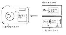
本例は、フラッシュメモリ10aのみを搭載したカード12aや、比較的小規模のロジック回路(ASIC)14を搭載したカード12bを対象とする。この場合、例えば、カード12a,12bが接続されるホスト側の機器をデジタルカメラ13と仮定すると、デジタルカメラ13の内部に配置されたフラッシュメモリカード制御用コントローラ11は、カード12a,12b内のフラッシュメモリ10a,10bに対して、ページイレーズ、ブロック内の部分イレーズのためのコマンドを供給する。
【0423】
図21の例は、本発明の例に関わる制御の全て又は一部を行う制御回路が搭載されたフラッシュメモリに関する。
【0424】
メモリカード12には、コントローラ11及びフラッシュメモリ10が搭載される。フラッシュメモリ10は、例えば、ページのデータ書き換え回数に関連付けられた情報を生成する制御回路15を有している。フラッシュメモリ10は、この制御回路15により、かかる情報を自ら作成し、かつ、この情報を、例えば、メモリセルアレイの冗長部(エラー訂正符合などの格納領域)に格納する。フラッシュメモリ10には、ページのデータ書き換え回数に関連付けられた情報を外部から参照できる機能を付加してもよい。
【0425】
ページのデータ書き換え回数に関連付けられた情報は、フラッシュメモリの外部からは直接参照することのできない特殊なメモリセル領域に格納されてもよい。この場合は、特定コマンドによって、かかる情報が外部に読み出せるようにしてもよいし、リフレッシュ条件が満たされたか否かに関わる情報を外部に読み出せるようにしてもよい。
【0426】
フラッシュメモリ10内の制御回路15は、例えば、特定コマンドの応答として、ページイレーズが可能であるか否か、ページイレーズが正常に行われたか否か、又は、ページイレーズが禁止され、実行されなかったか否かの情報を、コントローラ11に応答する機能を有していてもよい。
【0427】
この場合は、フラッシュメモリ(チップ)10の外部に設けられたコントローラ11は、特定コマンドに対する応答を解釈し、必要に応じて、リフレッシュ動作又はそれに相当する動作を実行する。
【0428】
また、フラッシュメモリ10に混載された制御回路15は、これまで説明を加えたような、ページのデータ書き換え回数に関連付けられた情報の保存に関する動作のみならず、リフレッシュ条件を判断する動作や、具体的なリフレッシュ動作などをコントロールするような機能を持っていてもよい。
【0429】
以上、本発明の例は、ページイレーズ機能を有する不揮発性半導体メモリと、データ書き換え回数に関連付けられた情報を管理するコントローラとを有するシステムであれば、どのようなものにも適用できる。
【0430】
また、上述の実施例では、主として、NAND型フラッシュメモリを前提として説明したが、本発明の例は、その他の不揮発性半導体メモリ、例えば、NOR型、AND型、DINOR型などの不揮発性半導体メモリにも適用可能である。また、不揮発性半導体メモリとしては、フラッシュメモリの他、近年、注目を浴びているメモリセルに磁性体を使用したMRAM(Magnetic Random Access Memory)及び(Resistance Random Access Memory)、メモリセルに強誘電体を使用したFeRAM(Ferroelectric Random Access Memory)や、メモリセルにカルコゲン化物などを使用したOUM( Ovonics Unified Memory)なども含まれる。
【0431】
このように、本発明の例によれば、ブロック内の1部分のイレーズが可能であり、データ更新の際、ブロック内の更新しないデータを別ブロックに退避させる頻度が減り、書き込み性能の大幅な向上が期待できる。
【0432】
【発明の効果】
以上、説明したように、本発明によれば、ページイレーズ機能を有するNAND型フラッシュメモリを使用するフラッシュメモリカードにおいて、ブロック内の各ページのデータ書き換え回数を一定条件内に制限することにより、ページイレーズ動作が他の非選択ページに与えるストレスに起因する問題を回避できる。これにより、比較的小さいサイズのデータ書き換えが頻繁に発生しても、書き込み性能の劣化が起こらないフラッシュメモリカードを提供できる。
【図面の簡単な説明】
【図1】本発明の例に関わるメモリセルアレイのデータ区分を示す図。
【図2】本発明の例に関わるシステムの概要を示す図。
【図3】本発明の実施の形態1に関わるデータ更新動作を示すフローチャート。
【図4】本発明の実施の形態2に関わるデータ更新動作を示すフローチャート。
【図5】実施の形態1,2に関わる実施例1のカウント動作を示す図。
【図6】実施の形態1,2に関わる実施例2のカウント動作を示す図。
【図7】実施の形態1,2に関わる実施例3のカウント動作を示す図。
【図8】本発明の実施の形態3に関わるデータ更新動作を示すフローチャート。
【図9】本発明の実施の形態4に関わるデータ更新動作を示すフローチャート。
【図10】実施の形態3,4に関わる実施例1のカウント動作を示す図。
【図11】実施の形態3,4に関わる実施例2のカウント動作を示す図。
【図12】実施の形態3,4に関わる実施例3のカウント動作を示す図。
【図13】その他の実施例1のカウント動作を示す図。
【図14】その他の実施例2のカウント動作を示す図。
【図15】その他の実施例2のカウント動作を示す図。
【図16】その他の実施例3のカウント動作を示す図。
【図17】その他の実施例3のカウント動作を示す図。
【図18】ページイレーズ時のコマンドの発生例を示す波形図。
【図19】本発明の例が適用されるメモリカードの例を示す図。
【図20】本発明の例が適用されるシステムの例を示す図。
【図21】本発明の例が適用されるメモリカードの例を示す図。
【図22】従来のメモリセルアレイの構成例を示す図。
【図23】NANDセルユニットの例を示す図。
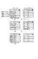
【符号の説明】
10,10a,10b:メモリ、 11:コントローラ、 12,12a,12b:メモリカード、 13:デジタルカメラ、 14:ASIC、 15:制御回路、 NU:NANDユニット、 WL0,WL1,・・・WL31:ワード線、 BL:ビット線、 SGD,SGS:セレクトゲート線、 SL:ソース線、 M0,M1,・・・M31:メモリセル、 ST1,ST2:セレクトゲートトランジスタ。[0001]
BACKGROUND OF THE INVENTION
The present invention relates to management of the number of rewrites (write / erase times) in a non-volatile semiconductor memory, and is particularly used for a NAND flash memory.
[0002]
[Prior art]
In recent years, flash memory cards using NAND flash memory have been used as storage media for various portable information terminals such as digital cameras. 22 and 23 show an outline of the memory cell arrangement of the NAND flash memory.
[0003]
The memory cell array of the NAND flash memory is composed of an assembly of basic units called NAND units NU. The NAND unit NU includes a cell column composed of a plurality of memory cells M0, M1,... M31 connected in series, and a total of two select gate transistors ST1, ST2 respectively connected to both ends of the cell column. Consists of
[0004]
In the NAND unit NU, two adjacent memory cells share one source / drain region. The select gate transistor ST1 is connected to the bit line BL, and the select gate transistor ST2 is connected to the source line SL.
[0005]
The memory cell array is divided into units of pages and blocks. A page means an aggregate of memory cells connected to one word line. A page is a basic unit for performing operations such as writing, erasing, and reading. The block means an aggregate of pages sandwiched between the bit line side select gate transistor ST1 and the source line side select gate transistor ST2.
[0006]
According to the example of FIG. 22, the memory cell array is composed of X + 1 blocks, and one block is composed of 32 pages. The data length of one page is 528 bytes. Of these, 512 bytes are a data area (user data portion) that can be freely used by the user, and the remaining 16 bytes are redundant portions. Generally, an ECC (Error Correction Circuit) code for error correction for a data area, a logical address, a flag indicating pass / fail of a block, and the like are stored in the redundant portion.
[0007]
In such a NAND flash memory, data erase is normally performed in units of blocks (block erase). In this case, in data rewriting in units smaller than a block, for example, page unit, cell data in a block including a page to be rewritten is temporarily saved in a data storage unit such as another block for rewriting. You must protect the cell data of pages that are not subject to.
[0008]
Therefore, this save operation takes a lot of time and hinders the improvement of the rewriting performance of the NAND flash memory.
[0009]
In order to solve this problem, in recent years, NAND flash memories capable of performing data erase in units of pages have been developed (see, for example,
[0010]
However, the NAND flash memory having the page erase function has the following problems in terms of reliability.
[0011]
When the write / erase operation is repeated only for one specific page in the selected block, pages other than the specific one page in the selected block, that is, rewriting targets The voltage stress (intermediate voltage) is repeatedly applied to the memory cells of the pages that do not become.
[0012]
For example, every time a data write is executed, an intermediate voltage smaller than the write voltage is applied to the memory cell of the page that is not the target of rewriting.
[0013]
As a result, the threshold state of the memory cell of the page not to be rewritten in the selected block gradually changes, and eventually the cell data is destroyed. For this reason, conventionally, it has been difficult to increase the rewrite speed of file data, for example, by using the page erase function.
[0014]
[Patent Document 1]
JP-A-3-295097
[0015]
[Patent Document 2]
JP-A-8-143398
[0016]
[Patent Document 1]
Japanese Patent Laid-Open No. 11-176177
[0017]
[Problems to be solved by the invention]
Thus, conventionally, there has been no effective technique for improving the rewrite performance of the nonvolatile semiconductor memory.
[0018]
An object of the present invention is to improve the data rewriting performance by utilizing the page erase function, and manage the number of times of data rewriting of pages in one block for each page, so that pages that are not subject to rewriting are managed. An object of the present invention is to propose a non-volatile semiconductor memory having a novel configuration capable of avoiding problems caused by voltage stress acting on memory cells.
[0019]
[Means for Solving the Problems]
In the nonvolatile semiconductor memory according to the example of the present invention, one block is composed of a plurality of pages, and data is rewritten in a page unit or a unit smaller than that, and data for each of the plurality of pages It has a control circuit that manages information associated with the number of rewrites for each page.
[0020]
DETAILED DESCRIPTION OF THE INVENTION
Hereinafter, a nonvolatile semiconductor memory according to an example of the present invention will be described in detail with reference to the drawings.
[0021]
1. Overview
The example of the present invention is applied to a NAND flash memory having a page erase function. That is, the NAND flash memory according to the example of the present invention uses the page erase function to improve the data rewrite performance. Further, the problem of voltage stress due to the page erase function is solved by managing the number of data rewrites of pages in one block for each page. Specific examples thereof will be described in each embodiment described later.
[0022]
The example of the present invention is particularly applied to a system in which rewriting of data with a small size (for example, rewriting of FAT (File Allocation Table) information) is frequently performed. This is because the page erase function mainly improves the performance of such rewriting of small size data. The example of the present invention is applied to a flash memory card and an electronic device using the same.
[0023]
2. Example of NAND flash memory
First, in describing an example of the present invention, an example of a NAND flash memory which is a premise thereof will be described.
[0024]
22 and 23 show examples of the memory cell array of the NAND flash memory.
[0025]
The memory cell array of the NAND flash memory is composed of an assembly of basic units called NAND units NU. The NAND unit NU includes a cell column composed of a plurality of memory cells M0, M1,... M31 connected in series, and a total of two select gate transistors ST1, ST2 respectively connected to both ends of the cell column. Consists of
[0026]
In the NAND unit NU, two adjacent memory cells share one source / drain region. The select gate transistor ST1 is connected to the bit line BL, and the select gate transistor ST2 is connected to the source line SL.
[0027]
The memory cell array is divided into units of pages and blocks. A page means an aggregate of memory cells connected to one word line. A page is a basic unit for performing operations such as writing, erasing, and reading. The block means an aggregate of pages sandwiched between the bit line side select gate transistor ST1 and the source line side select gate transistor ST2.
[0028]
According to the example of FIG. 22, the memory cell array is composed of X + 1 blocks, and one block is composed of 32 pages. The data length of one page is 528 bytes. Of these, 512 bytes are a data area (user data portion) that can be freely used by the user, and the remaining 16 bytes are redundant portions. Generally, an ECC (Error Correction Circuit) code for error correction for a data area, a logical address, a flag indicating pass / fail of a block, and the like are stored in the redundant portion.
[0029]
The NAND flash memory to which the example of the present invention is applied has a page erase function. In this case, when executing data rewriting in units smaller than a block, for example, in page units, in principle, cell data in a block including a page to be rewritten is temporarily stored in data such as another block. Therefore, the data rewrite speed can be increased.
[0030]
Here, the potential relationship during page erase and the potential relationship during subsequent writing will be described.
[0031]
At the time of page erase, for example, it is assumed that the cell data of
[0032]
As a result, a large potential difference occurs only between the word line WL0 and the well, and the cell data of only the memory cells connected to the word line WL0, that is, the memory cells in the
[0033]
The same can be done when erasing multiple pages simultaneously. In other words, the potential of the word line corresponding to the page to be erased may be set to the ground level, and the other word lines may be set to the high potential. For example, when erasing the cell data of
[0034]
Thus, in the page erase operation, only the cell data of one or more selected pages are erased in the same block, and the cell data of non-selected pages are protected as they are without being erased. .
[0035]
The write operation is executed for each page after page erase.
[0036]
For example, assume that a write operation is performed on
[0037]
As a result, a large potential difference is generated only between the word line WL0 and the well, and only the memory cell connected to the word line WL0, that is, the memory cell in the
[0038]
As described above, in the write operation, data is written to only one selected page in the selected block. At this time, voltage stress is applied to the memory cells of the remaining non-selected pages. The
[0039]
3. Simplification
Although the NAND flash memory to which the example of the present invention is applied has been described, in the embodiment described below, in order to simplify the description, as shown in FIG. Assuming that
[0040]
Further, in the example of the present invention, as described above, the problem of voltage stress caused by the page erase function is solved by managing the data rewrite frequency of the page in one block for each page. As shown in FIG. 1, the number of data rewrites is stored as a count value for each page in the redundant portion of the memory cell array.
[0041]
In the example of the present invention, this count value is important, and other data stored in the redundant portion, that is, a logical address, a flag indicating whether the block is good (block status), an ECC code, and the like are the same as in the past. . Therefore, in the embodiment described below, for the redundant portion, only the number of data rewrites, that is, the count value is shown for the sake of simplicity.
[0042]
In the description of the NAND flash memory, it has been described that voltage stress is applied to the memory cells of the non-selected page during the write operation. Here, the maximum number of times the memory cell can withstand this voltage stress without destroying the cell data, that is, the maximum number of data rewrites (write / erase times) that the memory cell in the non-selected page can experience ( Assume that the allowable value is 32 times.
[0043]
4).
The first embodiment will be described below.
[0044]
A feature of this embodiment is that, in a NAND flash memory having a page erase function, the number of data rewrites is managed in units of pages, and the number of data rewrites for each page in one block satisfies a predetermined condition. The refresh operation is performed for the one block.
[0045]
Here, data rewriting may be performed in units of one or a plurality of pages, or may be performed in units of blocks. The important point is that each time data rewriting is performed, the number of times of data rewriting is counted for each page with respect to the page on which data rewriting has been performed. As will be described later, the counting method is not particularly limited.
[0046]
In addition, the “refresh operation” referred to here is to rewrite data to a specific page (all pages or one or more pages) in one block. The meaning or purpose of the refresh operation is to refresh the data on the non-selected page before the data on the non-selected page is destroyed due to voltage stress. The same. The refresh operation method is not particularly limited as will be described later.
[0047]
FIG. 2 shows a system according to the first embodiment of the present invention. FIG. 3 shows the main part of the operation of the system according to the first embodiment of the present invention.
[0048]
The
[0049]
The
[0050]
First, when receiving a rewrite signal from the
[0051]
The
[0052]
Thereafter, data erase and data write are executed (steps ST3 to ST4).
[0053]
The data erase may be a page erase in which erase is executed in units of pages, or a block erase or chip erase in which erase is executed in units of blocks or chips. In short, it is sufficient that the
[0054]
Data write is executed in units of pages. When data rewriting is performed on a plurality of or all pages in the selected block, for example, data writing is performed page by page in order from the memory cell close to the source line. In the data write, new data is stored in the data area, and a new count value is stored in the redundant portion.
[0055]
Next, the
[0056]
When the number of data rewrites does not reach the maximum value (allowable value), nothing is particularly performed as the operation related to the present invention. That is, the
[0057]
When the number of data rewrites has reached the maximum value (allowable value), the
[0058]
5.
The second embodiment will be described below.
[0059]
This embodiment is a modification of the first embodiment. In this embodiment, the definition of words and other conditions in
[0060]
In the first embodiment, the refresh operation is performed when the number of data rewrites satisfies a predetermined condition.
[0061]
However, in this case, the refresh operation (erase and write) is continuously executed after the data rewrite (erase and write) is performed for the last page to be rewritten. That is, the last data rewrite operation is redundant.
[0062]
Therefore, in this embodiment, the data rewriting operation for the page to be subjected to the last data rewriting is performed during the refresh operation. In this way, useless data rewriting operation can be eliminated and data rewriting performance can be improved.
[0063]
FIG. 2 shows a system according to the second embodiment of the present invention. FIG. 4 shows the main part of the operation of the system according to the second embodiment of the present invention.
[0064]
Since the
[0065]
First, when receiving a rewrite signal from the
[0066]
The
[0067]
Next, the
[0068]
If the number of data rewrites has not reached the maximum value (allowable value), data erase and data write are executed (steps ST4 to ST5).
[0069]
The data erase may be a page erase in which erase is executed in units of pages, or a block erase or chip erase in which erase is executed in units of blocks or chips.
[0070]
Data write is executed in units of pages. When data rewriting is performed on a plurality of or all pages in the selected block, for example, data writing is performed page by page in order from the memory cell close to the source line. In the data write, new data is stored in the data area, and a new count value is stored in the redundant portion.
[0071]
If the number of data rewrites has reached the maximum value (allowable value), the
[0072]
The method of the refresh operation will be described in detail later. In the second embodiment, at least the page that is the target of data rewrite in the selected block is rewritten by this refresh operation. In addition, a normal refresh operation is executed for a page in the selected block that is not subject to data rewriting.
[0073]
When the refresh operation is performed, in principle, the number of data rewrites (count value) of each page in the selected block is initialized. However, depending on the counting method, the number of data rewrites may not be initialized.
[0074]
6). Examples related to
Examples relating to the first and second embodiments will be described below.
[0075]
(1) Example 1
▲ 1 ▼ Counting method
FIG. 5 shows a counting method according to the first embodiment of the present invention.
[0076]
In this example, the count value is stored in a redundant portion in the memory cell array of the NAND flash memory. The count value represents the number of data rewrites for a page and is stored for each page.
[0077]
The refresh is performed on the condition that the total count value of each page in the block has reached the maximum value (allowable value) of 32 times. That is, regarding the data rewriting operation, as a worst case, it is conceivable that at least one page is never selected. The memory cells in the unselected page can withstand voltage stress caused by data rewrite up to 32 times, and thus the above-described conditions are set.
[0078]
In the description of the first embodiment, the
[0079]
The reason why the
[0080]
The
[0081]
For example, the data stored in the
[0082]
(a) Initial state
All the memory cells in the physical addresses (pages) 0, 1, 2, and 3 in the block are in the erased state.
[0083]
(b) Light
First, data LA0 is written to
[0084]
When the data LA0 is written to the
[0085]
(c) and (d) Data rewrite of
The
[0086]
First, the count values of all
[0087]
Thereafter, the data LA0 stored at the
[0088]
2 calculates the total value of the count values of all
[0089]
Therefore, at this time, the refresh operation is not performed.
[0090]
(e) and (f) Data rewrite of
The
[0091]
The count values of all
[0092]
Thereafter, the data LA2 stored in the
[0093]
2 calculates the total value of the count values of all
[0094]
Therefore, the refresh operation is not performed even at this time.
[0095]
(g) Refresh
In accordance with the data update request, the above operations (c) and (d) or the same operations as (e) and (f) are executed, and finally the count values of
[0096]
When the
[0097]
In this example, the count values of the
[0098]
However, as described above, in the worst case, at least one physical address may not be selected in 32 data rewrite operations. In this case, the at least one physical address has been subjected to 32 voltage stresses in a state where it is not a data rewrite target.
[0099]
Therefore, when the total value of the count values of the
[0100]
In this example, all
[0101]
In other words, if the data destruction of the memory cell does not occur up to 32 voltage stresses, the refresh condition is that the total value of the count values of
[0102]
In this example, the refresh condition is based on the total value of the count values of
[0103]
In the refresh operation, the data stored in the data area is refreshed by rewriting, but the count value of the redundant portion is initialized to, for example, the state (b) at the time of the refresh operation. That is, in the write operation in refresh, the count value “1” is written to the redundant portions corresponding to the
[0104]
(2) Method of refresh operation
A refresh operation method will be described.
[0105]
As described above, the refresh is to rewrite data on all pages or one or more pages in a block. The purpose of the refresh is to refresh the data in the memory cell before the data in the memory cell is destroyed by the threshold fluctuation due to voltage stress. Any method can be used as long as this purpose can be realized. .
[0106]
(a) Refresh example 1
For example, after data of all physical addresses in a block to be refreshed is transferred to a memory (such as RAM) in the controller, data of all physical addresses in the block is erased. This erase may be a block erase or a page erase. Then, the data temporarily stored in the memory in the controller is returned again to the physical address in the block. As a result, the data in the memory cells constituting the physical address subject to refresh is refreshed.
[0107]
(b) Refresh example 2
First, after transferring data of all physical addresses in one block to be refreshed to other blocks not to be refreshed, data of all physical addresses in that one block is erased. This erase may be a block erase or a page erase. Then, the data temporarily stored in the other block is returned again to the physical address in one block. As a result, the data in the memory cells constituting the physical address subject to refresh is refreshed. In this example, one block and the other block may be formed in the same chip, or may be formed in different chips.
[0108]
(3) Refresh operation timing
The timing for performing the refresh operation is not particularly limited.
[0109]
For example, when the allowable value is “32”, if the total value of the count value of the physical address in the block reaches 32 times and the 32nd rewrite operation is completed, the refresh operation is immediately executed thereafter. Also good. Further, the refresh operation may be executed at an appropriate time after the 32nd rewrite operation is completed, for example, after access from the host is interrupted.
[0110]
In the case of the example based on the second embodiment, the 32nd data rewrite operation is performed in the refresh operation. For this reason, the refresh operation is immediately executed together with the 32nd rewrite operation after the total value of the count values of the physical addresses in the block reaches 32 times.
[0111]
▲ 4 ▼ Other
In this example, the count value starts from “0”, such as 0, 1, 2,..., And increases by “1” according to the number of data updates. It is not limited to how to count.
[0112]
For example, the initial value may be a numerical value other than “0”, for example, “2”, a binary number may be “10”, and the increment may be other numerical values, for example, “2” instead of “1”. " In this case, the maximum value (allowable value) of the number of data rewrites also naturally changes. In this example, the maximum count value is “32”. Therefore, it is sufficient for the redundant portion of the memory cell array to have a sufficient number of bits to count up to “32”. That is, for one physical address, 5 bits of the redundant part are used as an area for storing the count value.
[0113]
Further, the increment of the count value may not be an arithmetic progression.
[0114]
For example, when 4 bytes, that is, 32 bits of the redundant portion of the memory cell array are used as an area for storing the count value, the number of data rewrites is “1” among these 32 bits. You may judge by the number of bits.
[0115]
Specifically, the initial value of the count value corresponding to a predetermined physical address is set to “00000... 000 (32 bits)”, and “1” in this area is set according to the number of data updates. Increase the number. For example, when the number of data updates is one, “00000... 001” (the number of “1” s out of 32 bits is one), and when the number of data updates is two, “00000 · .. 011 ”(the number of“ 1 ”out of 32 bits is 2).
[0116]
Further, for example, when 4 bytes, that is, 32 bits of the redundant portion of the memory cell array are used as an area for storing the count value, the number of data rewrites is “1” in the 32 bits. The determination may be made based on the position of a certain bit.
[0117]
Specifically, the initial value of the count value corresponding to a predetermined physical address is set to “00000... 000 (32 bits)”, and “1” in this area is set according to the number of data updates. Change the position. For example, when the number of data updates is one, it is “00000... 001” (the position of “1” in the 32 bits is the right end). As the number of data updates increases, the position of “1” is shifted to the left one by one.
[0118]
Further, the count value may be decreased instead of being increased according to the number of data updates. For example, the initial value of the count value may be set to “32”, and this number may be decreased by 1 according to the number of data updates.
[0119]
(2) Example 2
▲ 1 ▼ Counting method
FIG. 6 shows a counting method according to the second embodiment of the present invention.
[0120]
In the first embodiment described above, the number of data rewrites is managed for each page, and the controller calculates the total number of data rewrites in the block based on the number of data rewrites for each page every time data is rewritten.
[0121]
On the other hand, in the second embodiment, the total value of the number of data rewrites in the block is managed. That is, the count value of the page subjected to data rewriting is set not to the number of data rewrites for the page but to the total value of the number of data rewrites in the block including the page.
[0122]
Therefore, the controller only has to select the maximum value Nmax from the count values of each page in the block every time data is rewritten.
[0123]
The refresh is performed on condition that the maximum value Nmax among the count values of each page in the block has reached the allowable value of 32 times. This is because, in the worst case regarding the data rewriting operation, there may be a case where at least one page is never selected. The memory cells in the unselected page can withstand voltage stress caused by data rewrite up to 32 times, and thus the above-described conditions are set.
[0124]
Also in the description of the second embodiment, the meanings of the
[0125]
(a) Initial state
All the memory cells in the physical addresses (pages) 0, 1, 2, and 3 in the block are in the erased state.
[0126]
(b) Light
First, data LA0 is written to
[0127]
When the data LA0 is written to the
[0128]
Similarly, when the data LA2 is written to the
[0129]
(c) and (d) Data rewrite of
The
[0130]
First, the count values of all
[0131]
Thereafter, the data LA0 stored at the
[0132]
Further, the
[0133]
Therefore, at this time, the refresh operation is not performed.
[0134]
(e) and (f) Data rewrite of
The
[0135]
First, the count values of all
[0136]
Thereafter, the data LA2 stored in the
[0137]
Further, the
[0138]
Therefore, at this time, the refresh operation is not performed.
[0139]
(g) Refresh
In accordance with the data update request, the above operations (c) and (d) or the same operations as (e) and (f) are executed, and finally the count values of
[0140]
When the
[0141]
In this example, the count values of the
[0142]
However, as described above, in the worst case, at least one physical address may not be selected in 32 data rewrite operations. In this case, the at least one physical address has been subjected to 32 voltage stresses in a state where it is not a data rewrite target.
[0143]
Therefore, when the maximum value Nmax of the count values of the
[0144]
In this example, all
[0145]
In other words, if the data destruction of the memory cell does not occur up to 32 voltage stresses, the refresh condition is that the maximum value Nmax of the count values of the
[0146]
In this example, the refresh condition is based on the maximum count value Nmax of the
[0147]
In the refresh operation, the data stored in the data area is refreshed by rewriting, but the count value of the redundant portion is initialized to, for example, the state (b) at the time of the refresh operation. That is, in the refresh write operation, the count values “1”, “2”, “3”, and “4” are written in the redundant portions corresponding to the
[0148]
(2) Method of refresh operation
As the refresh operation, any method may be used as long as the purpose of refreshing the data in the memory cell can be achieved before the data in the memory cell is destroyed due to threshold fluctuation due to voltage stress. For example, as the refresh operation method, Example 1 and Example 2 described in the first embodiment can be used as they are, and thus detailed description thereof is omitted.
[0149]
(3) Refresh operation timing
The timing for performing the refresh operation is not particularly limited.
[0150]
For example, when the allowable value is “32”, when the maximum value Nmax of the physical address count value in the block reaches 32 times and the 32nd rewrite operation is completed, the refresh operation is immediately executed thereafter. May be. Further, the refresh operation may be executed at an appropriate time after the 32nd rewrite operation is completed, for example, after access from the host is interrupted.
[0151]
In the case of the example based on the second embodiment, the 32nd data rewrite operation is performed in the refresh operation. For this reason, the refresh operation is immediately executed together with the 32nd rewrite operation after the maximum value Nmax of the count value of the physical address in the block reaches 32 times.
[0152]
▲ 4 ▼ Other
In this example, the count value starts from “0” such as 0, 1, 2,... And increases by “1” according to the number of data rewrites in the block. It is not limited to such a counting method.
[0153]
For example, as in the first embodiment, the initial value may be a numerical value other than “0”, for example, “2”, “10” in binary number, and the increment may be other than “1”. For example, “2” may be used. In this case, the allowable value of the number of data rewrites in the block naturally changes.
[0154]
In this example, the count value does not become larger than “32”. Therefore, as a redundant portion of the memory cell array, it is sufficient to secure the number of bits that can count up to “32”. That is, 5 bits of the redundant portion of the memory cell array may be used as an area for storing the count value.
[0155]
Further, the increment of the count value may not be an arithmetic progression. As described in the first embodiment, for example, 4 bytes of the redundant portion of the memory cell array, that is, 32 bits are used as an area for storing the count value. This may be determined by the number of bits in the “1” state. For example, the number of data rewrites may be determined based on the position of the bit in the “1” state among these 32 bits.
[0156]
Further, the count value may be decreased instead of being increased according to the number of data updates. For example, the initial value of the count value may be set to “32”, and this number may be decreased by 1 according to the number of data updates.
[0157]
(3) Example 3
▲ 1 ▼ Counting method
FIG. 7 shows a counting method according to the third embodiment of the present invention.
[0158]
In the above-described first and second embodiments, the worst condition is assumed, and a method of executing the refresh operation when the total value of the number of data rewrites in the block reaches an allowable value, for example, 32 times is adopted. In this case, when the total value of the number of data rewrites in the block reaches an allowable value, a refresh operation is always performed regardless of the number of data rewrites in each page.
[0159]
On the other hand, when there is no need to perform a refresh operation, for example, even if each page in the block is subject to data rewrite in a short cycle (less than 32 times), the number of data rewrites in the block is allowed. When the value is reached, it means that a refresh operation is necessarily performed. That is, a useless refresh operation may be performed.
[0160]
The third embodiment proposes a method for completely eliminating such a useless refresh operation.
[0161]
Regarding the counting method, the third embodiment is the same as the second embodiment. That is, the count value of the page that is the target of data rewrite is set not to the number of data rewrites for the page but to the total value of the number of data rewrites in the block including the page.
[0162]
However, in the third embodiment, the refresh generation condition is different from that in the second embodiment.
[0163]
In the second embodiment, the controller selects the maximum value Nmax from the count values of each page in the block every time data is rewritten, and the maximum value Nmax reaches an allowable value, for example, 32 times. Judged whether or not. On the other hand, in the third embodiment, the controller selects the maximum value Nmax and the minimum value Nmin from the count values of each page in the block every time data is rewritten, and the maximum value Nmax and the minimum value Nmin are selected. It is determined whether or not the difference between the values reaches an allowable value, for example, 32 times.
[0164]
Here, the count value being the maximum value Nmax means that the data update of the page corresponding to the count value was performed at the closest time to the present time. Further, the fact that the count value is the minimum value Nmin means that the data update of the page corresponding to the count value was performed at a time farthest from the current time.
[0165]
The difference between the maximum value Nmax and the minimum value Nmin means the number of data rewrites in the block after the last data update of the page having the count value of the minimum value Nmin. That is, the memory cell in the page whose count value is the minimum value Nmin is subjected to voltage stress for the number of times corresponding to the difference between the maximum value Nmax and the minimum value Nmin after the data update of the page is performed last. It will be.
[0166]
As described above, in the third embodiment, the maximum value Nmax and the minimum value Nmin are extracted from the count values of each page in the block, and the necessity of the refresh operation is determined based on the difference.
[0167]
The advantage of the third embodiment is that if the difference between the maximum value Nmax and the minimum value Nmin is less than the allowable value, the data rewrite operation can be continuously performed without executing the refresh operation. That is, in the third embodiment, the number of refresh operations can be significantly reduced by omitting a useless refresh operation as compared with the first and second embodiments.
[0168]
In the description of the third embodiment, the meanings of the
[0169]
(a) Initial state
All the memory cells in the physical addresses (pages) 0, 1, 2, and 3 in the block are in the erased state.
[0170]
(b) Light
First, data LA0 is written to
[0171]
When the data LA0 is written to the
[0172]
Similarly, when the data LA2 is written to the
[0173]
(c) and (d) Data rewrite of
The
[0174]
First, the count values of all
[0175]
Thereafter, the data LA0 stored at the
[0176]
Further, the
[0177]
At this time, the count value “5” of the
[0178]
Therefore, at this time, the refresh operation is not performed.
[0179]
(e) and (f) Data rewrite of
The
[0180]
First, the count values of all
[0181]
Thereafter, the data LA2 stored in the
[0182]
Further, the
[0183]
At this time, the count value “6” of the
[0184]
Therefore, at this time, the refresh operation is not performed.
[0185]
(g) Refresh
In accordance with the data update request, the above operations (c) and (d) or the same operations as (e) and (f) are executed, and finally the count values of
[0186]
The
[0187]
That is, after the data at the
[0188]
In this example, the necessity of the refresh operation is determined based on the difference between the maximum value Nmax and the minimum value Nmin of the count values of the
[0189]
In this example, since the necessity of the refresh operation is determined based on the difference between the maximum value Nmax and the minimum value Nmin of the count value, the refresh condition is the initial state of the memory as in the first and second embodiments. It does not depend on. In this example, as in the first and second embodiments, it is not necessary to set the refresh condition assuming the worst case.
[0190]
In the refresh operation, the data stored in the data area is refreshed by rewriting, but the count value of the redundant portion is initialized to, for example, the state (b) at the time of the refresh operation. That is, in the refresh write operation, the count values “1”, “2”, “3”, and “4” are written in the redundant portions corresponding to the
[0191]
In this example, when the refresh condition (Nmax−Nmin ≧ 32) described above is satisfied, refresh may be performed only for the physical address whose count value is the minimum value Nmin. In this case, after the refresh operation, only the count value of the physical address to be refreshed is updated, and the count is continuously performed without initializing other count values.
[0192]
For example, in the example of FIG. 7, only the physical address LA3 may be refreshed in (g), and the count value of the physical address LA3 may be set to “66” (= 65 + 1) by this refresh operation. . Since the data of the physical addresses LA0, LA1, and LA2 are not refreshed, the current state is maintained for the count value.
[0193]
(2) Method of refresh operation
As the refresh operation, any method may be used as long as the purpose of refreshing the data in the memory cell can be achieved before the data in the memory cell is destroyed due to threshold fluctuation due to voltage stress. For example, as the refresh operation method, Example 1 and Example 2 described in the first embodiment can be used as they are, and thus detailed description thereof is omitted.
[0194]
However, in this example, as described above, the refresh operation may be performed for all physical addresses in the block, and among the physical addresses in the block, only the physical address whose count value is the minimum value Nmin. You may go.
[0195]
(3) Refresh operation timing
The timing for performing the refresh operation is not particularly limited.
[0196]
For example, when the allowable value is “32”, if the difference between the maximum value Nmax and the minimum value Nmin of the count value of the physical address in the block reaches “32”, the refresh is performed immediately after the data rewrite operation is finished. An operation may be performed. In addition, the refresh operation may be executed at an appropriate time after the data rewrite operation is completed, for example, after access from the host is interrupted.
[0197]
In the example based on the second embodiment, the data rewrite operation when the difference between the maximum value Nmax and the minimum value Nmin reaches “32” is performed in the refresh operation. For this reason, the refresh operation is executed immediately when the difference between the maximum value Nmax and the minimum value Nmin of the count values of the physical addresses in the block reaches “32”.
[0198]
▲ 4 ▼ Other
In this example, the count value starts from “0” such as 0, 1, 2,... And increases by “1” according to the number of data rewrites in the block. It is not limited to such a counting method.
[0199]
For example, as in the first embodiment, the initial value may be a numerical value other than “0”, for example, “2”, and the increment is not “1” but another numerical value, for example, “2”. "
[0200]
In this example, if the maximum value Nmax−minimum value Nmin does not satisfy the refresh condition, the count value increases without limit. However, the number of bits of the redundant part for storing the count value is limited.
[0201]
Therefore, for example, when the count value reaches the upper limit value determined by the number of bits of the redundant portion for storing it, refresh is performed for all physical addresses in the block regardless of the above-described refresh conditions, and The count values of all physical addresses may be initialized.
[0202]
The increment of the count value may not be an arithmetic progression. As described in the first embodiment, for example, 4 bytes of the redundant portion of the memory cell array, that is, 32 bits are used as an area for storing the count value. This may be determined by the number of bits in the “1” state. For example, the number of data rewrites may be determined based on the position of the bit in the “1” state among these 32 bits.
[0203]
Further, the count value may be decreased instead of being increased according to the number of data updates. For example, the initial value of the count value may be an upper limit value determined by the number of bits of the redundant part for storing the count value, and this number may be decreased by 1 according to the number of data updates.
[0204]
7).
Hereinafter, the third embodiment will be described.
[0205]
The third embodiment relates to a system that can cope with power-off (during a memory card, including unintentional extraction from the main body) during data update.
[0206]
As a data update (data rewrite) method, as described in Examples 1, 2, and 3 related to
[0207]
In this case, if a power interruption occurs between step b. And step c., All of the old data, new data, old count value, and new count value are related to the physical address to be updated. It will disappear.
[0208]
As will be described later, the example of the present invention is effective for updating FAT (File Allocation Table) information, which is relatively small in capacity and frequently updated, when applied to file updating on a personal computer or the like. It seems to become. However, by applying the example of the present invention, if data is lost due to power interruption or the like, a system such as a personal computer will be fatally damaged.
[0209]
The third embodiment is an improved example in which the first embodiment is improved so as to be able to cope with such power-off.
[0210]
The following third embodiment will mainly describe the data update method, but can also be applied to the refresh method. That is, according to the third embodiment, it is possible to cope with the power interruption during the refresh operation by the same principle.
[0211]
Since the definition and meaning of the refresh operation are the same as those in the first embodiment, they are omitted here.
[0212]
FIG. 2 shows a system according to the third embodiment of the present invention. FIG. 8 shows the main part of the operation of the system according to the third embodiment of the present invention.
[0213]
Since the
[0214]
In the third embodiment, as a precondition, two memory areas (non-volatile) are used in pairs. Each memory area has one or more pages. Further, the two memory areas have the same number of pages.
[0215]
Both of the two memory areas may be arranged in one block of the
[0216]
First, when receiving a rewrite signal from the
[0217]
The
[0218]
When data rewriting is performed on a page in one memory area, data write is performed on a page in another memory area that is paired with the one memory area. In the data write, new data is stored in the data area, and a new count value is stored in the redundant portion.
[0219]
Data erase is performed after the data write.
Data erasure is performed on pages in one memory area. The data erase may be a page erase in which erase is executed in units of pages, or a block erase or chip erase in which erase is executed in units of blocks or chips.
[0220]
Next, the
[0221]
When the number of data rewrites does not reach the maximum value (allowable value), nothing is particularly performed as the operation related to the present invention. That is, the
[0222]
When the number of data rewrites has reached the maximum value (allowable value), the
[0223]
As described above, in the third embodiment, two memory areas are used in pairs, and new data and a new count value are always written to one of the two memory areas and then stored in the other of the two memory areas. The old data and the old count value are erased. For this reason, even if the power is cut off during the data rewriting operation, the data and the count value are stored in at least one of the two memory areas. There is no damage.
[0224]
8).
Hereinafter, the fourth embodiment will be described. This embodiment is a modification of the third embodiment. Since the definition and meaning of the refresh operation are the same as those in the first embodiment, they are omitted here.
[0225]
In the third embodiment, the refresh operation is performed when the number of data rewrites satisfies a predetermined condition. On the other hand, in the fourth embodiment, the last data rewrite operation in which the count value reaches the allowable value is performed during the refresh operation.
[0226]
In the third embodiment, two memory areas (non-volatile) are used in pairs in order to prevent data loss due to unexpected interruption of the power supply, etc., and in the data update operation, the erase operation is performed after the write operation. ing. However, the refresh operation is performed simultaneously on the two memory areas.
[0227]
Therefore, in the fourth embodiment, for the last data update operation in which the count value reaches the allowable value, for example, a refresh operation (including a data rewrite operation) is executed by the same method as in the second embodiment.
[0228]
However, if there is an unused memory area (non-volatile), at the time of refreshing, new data and a new count value are written to the unused memory area, and then the data and count value in the two memory areas are erased. Also good.
[0229]
FIG. 2 shows a system according to the fourth embodiment of the present invention. FIG. 9 shows the main part of the operation of the system according to the fourth embodiment of the present invention.
[0230]
Since the
[0231]
First, when receiving a rewrite signal from the
[0232]
Next, the
[0233]
If the number of data rewrites has not reached the maximum value (allowable value), data write and data erase are executed (steps ST4 to ST5).
[0234]
When data rewriting is performed on a page in one memory area, data write is performed on a page in another memory area that is paired with the one memory area. In the data write, new data is stored in the data area, and a new count value is stored in the redundant portion.
[0235]
Data erase is performed after the data write.
Data erasure is performed on pages in one memory area. The data erase may be a page erase in which erase is executed in units of pages, or a block erase or chip erase in which erase is executed in units of blocks or chips.
[0236]
If the number of data rewrites has reached the maximum value (allowable value), the
[0237]
When the refresh operation is performed, in principle, the data rewrite count (count value) of each page in the two memory areas is initialized. However, depending on the counting method, the number of data rewrites may not be initialized.
[0238]
9. Examples related to
Examples relating to the third and fourth embodiments will be described below.
[0239]
(1) Example 1
(1) Data update method
FIG. 10 shows a data update method according to the first embodiment of the present invention.
[0240]
In this example, the method of Example 2 relating to
[0241]
In this example, one block has four physical addresses, but only one half of the data, that is, data for two physical addresses (two pages) is stored in the one block. In this respect, this example is different from Examples 1, 2, and 3 related to
[0242]
Physical addresses 0 and 1 make up one memory area, and
[0243]
(a) Initial state
All the memory cells in the physical addresses (pages) 0, 1, 2, and 3 in the block are in the erased state.
[0244]
(b) Light
First, data LA0 is written to
[0245]
(b) and (c) Data rewrite of
The
[0246]
First, the count values of all
[0247]
Thereafter, the update data LA0 and the count value (= “3”) are written to the physical address 2 (see (c)). Thereafter, the data LA0 stored in the
[0248]
Further, the
[0249]
Therefore, at this time, the refresh operation is not performed.
[0250]
(c) and (d) Data rewrite of
The
[0251]
First, the count values of all
[0252]
Thereafter, the update data LA1 and the count value (= “4”) are written to the physical address 3 (see (d)). Thereafter, the data LA1 stored in the
[0253]
Further, the
[0254]
Therefore, at this time, the refresh operation is not performed.
[0255]
(d) and (e) Data rewrite of
The
[0256]
First, the count values of all
[0257]
Thereafter, the update data LA0 and the count value (= “5”) are written to the physical address 0 (see (e)). Thereafter, the data LA0 and count value stored in the
[0258]
Further, the
[0259]
Therefore, at this time, the refresh operation is not performed.
[0260]
(e) and (f) Data rewrite of
The
[0261]
First, the count values of all
[0262]
Thereafter, the update data LA1 and the count value (= “6”) are written to the physical address 1 (see (f)). Thereafter, the data LA1 and count value stored in the
[0263]
Further, the
[0264]
Therefore, at this time, the refresh operation is not performed.
[0265]
(g) Refresh
It is assumed that the above operation is repeatedly executed according to the data update request, and finally the count values of the
[0266]
When the
[0267]
For the refresh operation, the same method as in Examples 1, 2, and 3 relating to
[0268]
For example, it is assumed that the count values of the
[0269]
Thereafter, the
[0270]
Thus, the refresh operation ends.
[0271]
As described above, in the first embodiment, new data is always written to the flash memory and then old data is erased. Therefore, even if the power is cut off at the stage of writing new data to the flash memory, the state immediately before the data update is saved at least, so fatal damage to the system is avoided. .
[0272]
The first embodiment is effective when rewriting logical data having a sufficiently smaller capacity than the block capacity. This is because in such a case, two memory areas constituting a pair in this embodiment can be arranged in one block.
[0273]
(2) Method of refresh operation
As described above, as the refresh operation method, Example 1 and Example 2 described in Example 1 regarding
[0274]
(3) Refresh operation timing
The timing for performing the refresh operation is not particularly limited.
[0275]
For example, when the allowable value is “32”, when the maximum value Nmax of the physical address count value in the block reaches 32 times and the 32nd rewrite operation is completed, the refresh operation is immediately executed thereafter. May be. Further, the refresh operation may be executed at an appropriate time after the 32nd rewrite operation is completed, for example, after access from the host is interrupted.
[0276]
In the example based on the fourth embodiment, the 32nd data rewrite operation is performed in the refresh operation. For this reason, the refresh operation is immediately executed together with the 32nd rewrite operation after the maximum value Nmax of the count value of the physical address in the block reaches 32 times.
[0277]
▲ 4 ▼ Other
In this example, the count value starts from “0” such as 0, 1, 2,... And increases by “1” according to the number of data rewrites in the block. It is not limited to such a counting method.
[0278]
For example, the initial value may be a numerical value other than “0”, for example, “2”, and the increment may be other than “1”, as in Example 1 relating to the first and second embodiments. For example, “2” may be used. In this case, the allowable value of the number of data rewrites in the block naturally changes.
[0279]
In this example, the count value does not become larger than “32”. Therefore, as a redundant portion of the memory cell array, it is sufficient to secure the number of bits that can count up to “32”. That is, 5 bits of the redundant portion of the memory cell array may be used as an area for storing the count value.
[0280]
Further, the increment of the count value may not be an arithmetic progression. As described in the first embodiment, for example, 4 bytes of the redundant portion of the memory cell array, that is, 32 bits are used as an area for storing the count value. This may be determined by the number of bits in the “1” state. For example, the number of data rewrites may be determined based on the position of the bit in the “1” state among these 32 bits.
[0281]
Further, the count value may be decreased instead of being increased according to the number of data updates. For example, the initial value of the count value may be set to “32”, and this number may be decreased by 1 according to the number of data updates.
[0282]
(2) Example 2
FIG. 11 shows a data update method according to the second embodiment of the present invention.
[0283]
In this example, as the counting method, the method of Example 1 relating to
[0284]
In this example, two different blocks A and B are used as a pair. These two blocks A and B may be arranged in one NAND type flash memory or in different NAND type flash memories. Each block A and B has four physical addresses.
[0285]
In this example, when data is rewritten a plurality of times for a specific physical address, data is alternately written to the two blocks A and B every time, and the old data is written. After that, erase each time. The count value is updated at the odd-numbered write. For example, when writing is started from the block A side, the count value is updated only when writing to the block A, and the count value is not updated when writing to the block B.
[0286]
(a) Initial state
Data LA0 is written to
[0287]
(b) -1 Data rewrite of
The
[0288]
First, the count value of
[0289]
Here, at the time of writing to the block B, the count value is not updated. That is, the count value of the
[0290]
Thereafter, the data LA0 and count value stored in the
[0291]
Further, the
[0292]
Therefore, at this time, the refresh operation is not performed.
[0293]
(b) -2 Data rewrite of
The
[0294]
First, the count value of the
[0295]
Further, the
[0296]
Therefore, at this time, the refresh operation is not performed.
[0297]
(b) -3 Data rewrite of
The
[0298]
First, the count value of the
[0299]
Further, the
[0300]
Therefore, at this time, the refresh operation is not performed.
[0301]
(c) -1 Data rewrite of
The
[0302]
First, the count value of
[0303]
When controlled in this way, the count value represents the number of rewrites to the physical address i in the block A or the number of rewrites to the physical address i in the block B. That is, the data is stored in one of the blocks A and B, and the count value at that time represents the number of data rewrites for the physical address i in the blocks A and B.
[0304]
Thereafter, the data LA0 and the count value stored at the
[0305]
Further, the
[0306]
Therefore, at this time, the refresh operation is not performed.
[0307]
(c) -2 Data rewrite of
The
[0308]
First, the count value of the
[0309]
Further, the
[0310]
Therefore, at this time, the refresh operation is not performed.
[0311]
(d) Refresh
It is assumed that the above operation is repeatedly executed according to the data update request, and finally the count values of the
[0312]
The number of data rewrites is as follows. In block A,
[0313]
In block B,
[0314]
In block A, since the data rewrite operation is performed 32 times in total, the refresh operation is executed for both blocks A and B thereafter.
[0315]
For example, after collecting data of all
[0316]
In addition, after data of all
[0317]
In this example, the data update is continued using the two blocks A and B as a pair. Block A and block B may exist in the same flash memory chip or in different flash memory chips. When there are a plurality of flash memory chips in the system (for example, a flash memory card), the blocks A and B may be allocated to different flash memory chips in the system. In this case, it is possible to contribute to improving the performance of the system, such as performing page erase for the block A during the write operation for the block B.
[0318]
(3) Example 3
FIG. 12 shows a data update method according to the third embodiment of the present invention.
[0319]
In this example, for example, another block of the NAND flash memory is used like a buffer. Here, a block that performs data update is referred to as a block A, and a block that is used as a data buffer for temporary storage when data is updated is referred to as a buffer block.
[0320]
(a) Initial state
The
[0321]
(b) to (d) Data rewrite of
The
[0322]
First, the count values of all
[0323]
Thereafter, the old data LA0 and the count value of the
[0324]
Further, the count value of the
[0325]
Thereafter, the update data LA0 and the count value of the
[0326]
Such an operation is repeated, and when the count values of the
[0327]
10. Other examples
Examples 1, 2, and 3 related to
[0328]
(1)
FIG. 13 shows a data update method according to another
[0329]
First, as a block configuration example, the page size is 512 bytes (528 bytes when the redundant part is added), and the block size is 16 kilobytes (excluding the redundant part). One block is composed of 32 pages.
[0330]
The file data is different from the FAT information as follows.
(1) When an update request for file data occurs, old data before update is no longer necessary.
(2) File data has a significantly lower frequency of data update for the same logical address than FAT information.
(3) Even if update data or old data is lost due to power interruption or the like, there is no fatal damage to the system because the update data exists inside the host system.
[0331]
Therefore, when updating file data, it is conceivable that restrictions are relaxed compared to updating FAT information.
[0332]
In Examples 1, 2, and 3 related to
[0333]
In this example, it is assumed that data update is performed in units of 8 pages. These eight pages (physical addresses) correspond to one grid in FIG. Therefore, FIG. 13 is almost the same as the drawings used in Examples 1, 2, and 3 related to
[0334]
(a) Initial state
The memory cells in all physical addresses (pages) 0 to 7, 8 to 15, 16 to 23, and 24 to 31 in the block are in an erased state.
[0335]
(b) Light
Data LA64 to 71 are written to
[0336]
(c) and (d) Data rewrite of physical addresses 8-15
The
[0337]
Data of
[0338]
As described above, in this example, the number of data rewrites for each page is not managed. The effect is as follows.
[0339]
For example, it is assumed that a data update request is generated for the
[0340]
That is, in the conventional method, when data is updated, copy operations for the data LA64 to LA71 and LA80 to LA95 that do not need to be updated occur, leading to a decrease in data rewrite speed.
[0341]
In contrast, according to this example, only the
[0342]
Here, the term “page erase” includes a partial erase in which a plurality of pages in a block are erased together, as well as an erase intended for only one page in a block. In addition, when erasing a plurality of pages in a block at a time, it may be erased at one time by partial erasing, or page erasing is performed by dividing each page into a plurality of times (here, 8 times). Also good. In such a case, erasing may be performed in two pages at a time, divided into a plurality of times (here, four times).
[0343]
Also, for example, in the case of a multi-level flash memory in which one bit line is shared by a plurality of sense amplifiers, when page erase is executed physically, the data for a plurality of pages is batched in terms of external specifications. It was erased at. Even in such a case, from the viewpoint of erasing only a part of the block instead of erasing all the pages in the block, this is equivalent to the erase of this example.
[0344]
In the field of digital cameras and the like where flash memory cards are often used, there are many usage methods such as taking pictures as much as the capacity of the memory card, transferring images to a system such as a personal computer, and erasing all image files. In such a case, the number of data rewrites to the flash memory is limited, and writing concentration in the area of the file body does not occur.
[0345]
Therefore, in the case of file data, there is no practical problem even if the number of data rewrites per page is not managed as in this example. This example is effective in such a field.
[0346]
Of course, for file data update, as shown in Examples 1, 2, 3 of
[0347]
In the following, an embodiment for managing the number of data rewrites when updating file data will be described.
[0348]
(2)
14 and 15 show a data update method according to another
[0349]
The data update method and count method of this example are the same as the method of Example 3 (see FIG. 7) related to the first and second embodiments. However, in this example, one page in Example 3 relating to the first and second embodiments is replaced with one partial erase erase unit (referred to as “one area”). In other words, in this example, one area includes a plurality of pages and is the minimum unit of erase.
[0350]
(a) Initial state
All the areas in the block, that is, the memory cells in the physical addresses (pages) 0 to 31 are in the erased state.
[0351]
(b) Light
First, data LA64 to LA71 (eight sectors if one sector is 512 bytes) are written to physical addresses (one area) 0-7. Similarly, data LA72 to LA79 are written to physical addresses (1 area) 8 to 15, data LA80 to LA87 are written to physical addresses (1 area) 16 to 23, and data are stored to physical addresses (1 area) 24 to 31. LA88 to LA95 are written.
[0352]
When the data LA64 to LA71 are written to the
[0353]
Similarly, when the data LA80 to LA87 are written to the
[0354]
(c) and (d) Data rewrite of physical addresses 0-7
The
[0355]
First, the count values of all
[0356]
Thereafter, the data LA64 to LA71 and count values stored in the
[0357]
2 extracts the maximum value Nmax and the minimum value Nmin from the count values of the
[0358]
At this time, the count value “5” of the
[0359]
Therefore, at this time, the refresh operation is not performed.
[0360]
(e) and (f) Data rewrite of
The
[0361]
First, the count values of all
[0362]
Thereafter, the data LA80 to LA87 and the count value stored in the
[0363]
2 extracts the maximum value Nmax and the minimum value Nmin from the count values of the
[0364]
At this time, the count value “6” of the
[0365]
Therefore, at this time, the refresh operation is not performed.
[0366]
(g) Refresh
In accordance with the data update request, the above-described operations (c) and (d) or the same operations as the operations (e) and (f) are executed. Finally,
[0367]
The
[0368]
That is, after the data at the physical addresses 24 to 31 is updated last, the physical addresses 24 to 31 are subjected to voltage stress due to 32 (= 65-33) data rewrites. Accordingly, when the
[0369]
In this example, the necessity of the refresh operation is determined based on the difference between the maximum value Nmax and the minimum value Nmin of the count values of the
[0370]
In this example, since the necessity for the refresh operation is determined based on the difference between the maximum value Nmax and the minimum value Nmin of the count value, the refresh condition does not depend on the initial state of the memory. In this example, it is not necessary to set the refresh condition assuming the worst case.
[0371]
In the refresh operation, the data stored in the data area is refreshed by rewriting, but the count value of the redundant portion is initialized to, for example, the state (b) at the time of the refresh operation. That is, as shown in (h) and (i) of FIG. 15B, in the write operation in the refresh, the redundant portions corresponding to the
[0372]
In this example, when the refresh condition (Nmax−Nmin ≧ 32) is satisfied, refresh may be performed only for the physical addresses 24 to 31 whose count value is the minimum value Nmin. In this case, as shown in (h) and (i) of FIG. 15 (A), after the refresh operation, only the count value of the physical addresses 24 to 31 to be refreshed is updated, and the other counts are updated. It continues to count without initializing the value.
[0373]
For example, in the example of (h) and (i) of FIG. 15A, the count value of the physical addresses LA24 to 31 is set to “66” (= 65 + 1) by the refresh operation of the physical addresses LA24 to 31. Good. Since the
[0374]
In this way, in this example, the number of data rewrites is stored for each area, and each time a data rewrite request is generated, the maximum value Nmax and the minimum value Nmin of the number of data rewrites (count value) are extracted, and the difference between them is extracted. The necessity of the refresh operation is judged. The advantage of this example is that if the difference between the maximum value and the minimum value is less than the allowable value, the data rewrite operation can be continued without executing the refresh operation.
[0375]
The number of data rewrites may be managed for each page constituting the area. This is because the size of the area in the block does not necessarily have to be fixed and may be variable. For example, if the area size is fixed, the number of data rewrites may be managed in units of areas, but if the area size is variable, the number of data rewrites is managed for each page in the area. Is convenient.
[0376]
As for the refresh method, various methods can be adopted as described above. For example, the data in the area to be refreshed is temporarily saved in a buffer in the system, and then the area is erased. Finally, the data is returned from the buffer in the system to the area again. This method can be adopted. Further, two blocks may be used in pairs, and the data in the area to be refreshed may be moved to another block.
[0377]
The embodiment has been described with the file body in mind. This example corresponds to Example 3 related to
[0378]
(3)
16 and 17 show a data update method according to another
[0379]
The basic algorithm is the same as Example 3 (see FIG. 12) related to
[0380]
(a) Initial state
The block A is as follows.
[0381]
The physical addresses (one area) 0 to 7 store data LA64 to LA71 (if one sector is 512 bytes, 8 sectors). Similarly, data LA72 to LA79 are stored in physical addresses (1 area) 8 to 15, data LA80 to LA87 are stored in physical addresses (1 area) 16 to 23, and data are stored in physical addresses (1 area) 24 to 31. LA88 to LA95 are stored.
[0382]
The count value of the
[0383]
For the buffer block, all
[0384]
(b) to (e) Data rewrite of
The
[0385]
First, the count values of all
[0386]
For example, the
[0387]
The update data LA64 to 71 and the count value “5” of the
[0388]
Thereafter, the data LA64 to LA71 and the count value stored in the
[0389]
Then, the
[0390]
Therefore, at this time, the refresh operation is not performed.
[0390]
Such an operation is repeated, and when the count values of the
[0392]
It is assumed that the data and the count value in the block A are finally as shown in (f) of FIG. In (f), the count values of the physical addresses 24 to 31 are the smallest and the oldest. On the other hand, the count values of the
[0393]
Thus, in this example, the maximum value Nmax and the minimum value Nmin of the number of data rewrites in each area in the block are extracted, and the necessity of the refresh operation is determined based on the difference. The advantage of this example is that, if the difference between the maximum value Nmax and the minimum value Nmin is less than the allowable value, data rewriting can be performed continuously without executing the refresh operation.
[0394]
In this example, since the necessity for the refresh operation is determined based on the difference between the maximum value Nmax and the minimum value Nmin of the count value, the refresh condition does not depend on the initial state of the memory. In this example, it is not necessary to set the refresh condition assuming the worst case.
[0395]
In the refresh operation, the data stored in the data area is refreshed by rewriting, but the count value of the redundant portion is initialized to, for example, the state (b) at the time of the refresh operation. That is, in the write operation in the refresh, the count values “1”, “2”, “3”, “4” are respectively applied to the redundant portions corresponding to the
[0396]
In this example, when the refresh condition (Nmax−Nmin ≧ 32) is satisfied, the refresh may be performed only for the physical addresses 24 to 31 whose count value is the minimum value Nmin. In this case, as shown in (f) and (g) of FIG. 17, after the refresh operation, only the count values of the physical addresses 24 to 31 subject to refresh are updated, and other count values are initialized. Without counting, it continues to count.
[0397]
For example, in the example of (f) and (g) in FIG. 15, the count value of the physical addresses LA24 to 31 may be set to “66” (= 65 + 1) by the refresh operation of the physical addresses LA24 to 31. Since the
[0398]
The number of data rewrites may be managed for each page constituting the area. This is because the size of the area in the block does not necessarily have to be fixed and may be variable. For example, if the area size is fixed, the number of data rewrites may be managed in units of areas, but if the area size is variable, the number of data rewrites is managed for each page in the area. Is convenient.
[0399]
As for the refresh method, various methods can be adopted as described above. In this example, as shown in (g) and (h) of FIG. 17, the data of the area to be refreshed is temporarily saved in the buffer block, and then the erase of the area is executed. The method of returning data from the buffer to the area again and finally erasing the buffer block is employed.
[0400]
In the
[0401]
In this case, data that is not updated in the area is saved in, for example, a buffer in the system or another block (buffer block), and is written back in the original block together with the updated data. In addition, when two blocks are used in pairs and data is written alternately, in the write operation for one block, update data and non-update data read from the other block are written. become.
[0402]
For example, in Examples 1, 2, and 3 related to
[0403]
11. Other
A count value indicating the number of data rewrites (which may be the number of erasures or the number of writes) for each page or area is usually stored in a redundant portion existing on the same page as the page storing data. However, the count value may be stored in a portion other than the redundant portion existing on the same page as the page storing data.
[0404]
For example, a memory area for centrally managing the number of data rewrites for each page or area may be provided in the flash memory, and the number of data rewrites may be managed in the memory area. Further, when a flash memory has a logical address / physical address conversion table, the number of data rewrites may be managed as an element constituting the table.
[0405]
The example of the present invention is mainly applied to updating user data, that is, file main body data, file management information (FAT table information, directory information), etc. in the case of a personal computer. However, the example of the present invention is not limited to such updating of user data, but updating of data not directly related to user data, for example, updating of management information used inside the card if it is a flash memory card It can also be applied.
[0406]
Management information used inside the card includes, for example, logical / physical address conversion table information, card attribute information and its update information, write protection information, security related information such as passwords, internal flash memory defects, etc. There are block management information, information such as the number of times data is rewritten in the flash memory, and control firmware for the controller inside the flash memory card.
[0407]
The example of the present invention can also be used in combination with conventional block-unit data rewriting. For example, the data of the file main body for which a write request is made in a relatively large unit, for example, a cluster unit, is supported by the conventional data rewriting in block units, and the FAT in which a write request is made in a relatively small unit Data, directory information, and the like correspond by data rewriting using page erase related to the example of the present invention.
[0408]
In this case, a function for analyzing the data structure is added to the controller, and if the FAT data or directory (including subdirectory information) is updated, the algorithm according to the example of the present invention may be activated. Further, if it is within the range of a preset logical address, it may be determined as FAT or directory information and the algorithm of the present invention may be activated.
[0409]
In each of the above-described embodiments, the NAND flash memory whose flash memory page size is 512 bytes (excluding the redundant portion) is taken as an example. However, with the recent increase in memory capacity, a flash memory having a page size of 2 kilobytes and a flash memory capable of simultaneously writing data to a plurality of pages have been developed.
[0410]
The example of the present invention can also be applied to such a new flash memory in recent years. For example, the page size is 2 kilobytes, one block is 64 pages, the block size is 128 kilobytes, and the size of the partial erase (erase unit) in the block may be applied to a 16 kilobyte NAND flash memory. it can.
[0411]
In this case, as external specifications, data for 8 pages is erased at once. However, for example, in the case of a binary flash memory in which one bit line is shared by two sense amplifiers, physically four pages are erased.
[0412]
In the erase operation, the word line (control gate electrode) of the page to be erased is actually set to the ground level, and the substrate is set to a high potential (for example, about 20 V). At this time, since a large potential difference is generated between the floating gate electrode and the substrate, the charge of the floating gate electrode is discharged by the FN tunneling phenomenon, and the data of the memory cell is erased.
[0413]
For example, the word lines of the pages that are not to be erased are set to the same potential as the substrate (for example, about 20 V). For this reason, in a page that is not to be erased, a large potential difference does not occur between the floating gate electrode and the substrate, and data in the memory cell is not erased.
[0414]
The example of the present invention is not limited to the page size of 2 kilobytes, but can be applied to a flash memory of any size.
[0415]
FIG. 18 shows an example of command generation during page erase of the NAND flash memory.
[0416]
Block erase, page erase, and partial erase within a block that simultaneously erases a plurality of pages are distinguished by different command codes.
[0417]
19 to 21 show an example of a system to which the example of the present invention is applied.
The example of FIG. 19 relates to a memory card having a controller and flash memory.
[0418]
The
[0419]
In this example, a controller (generally equipped with a microcomputer) 11 in the
[0420]
The
[0421]
The example of FIG. 20 relates to a memory card not equipped with a controller.
[0422]
This example is intended for a card 12a on which only the
[0423]
The example of FIG. 21 relates to a flash memory equipped with a control circuit that performs all or part of the control related to the example of the present invention.
[0424]
A
[0425]
Information associated with the number of page data rewrites may be stored in a special memory cell area that cannot be directly referenced from outside the flash memory. In this case, such information may be read to the outside by a specific command, or information relating to whether or not the refresh condition is satisfied may be read to the outside.
[0426]
For example, as a response to a specific command, the
[0427]
In this case, the
[0428]
In addition, the
[0429]
As described above, the example of the present invention can be applied to any system as long as it has a nonvolatile semiconductor memory having a page erase function and a controller that manages information associated with the number of data rewrites.
[0430]
In the above-described embodiments, the NAND flash memory has been mainly described. However, the examples of the present invention are other nonvolatile semiconductor memories, for example, nonvolatile semiconductor memories such as NOR type, AND type, and DINOR type. It is also applicable to. In addition to flash memory, non-volatile semiconductor memories include MRAM (Magnetic Random Access Memory) and Magnetic Random Access Memory (MRAM) that use magnetic materials for memory cells that have recently attracted attention. And FeRAM (Ferroelectric Random Access Memory) using the ORAM and OUM (Ovonics Unified Memory) using a chalcogenide in the memory cell.
[0431]
As described above, according to the example of the present invention, it is possible to erase a part of a block, and when updating data, the frequency of saving non-updated data in the block to another block is reduced, and the writing performance is greatly improved. Improvement can be expected.
[0432]
【The invention's effect】
As described above, according to the present invention, in a flash memory card using a NAND flash memory having a page erase function, the number of data rewrites of each page in a block is limited within a certain condition, Problems due to the stress that the erase operation gives to other non-selected pages can be avoided. As a result, it is possible to provide a flash memory card that does not deteriorate the writing performance even if data rewriting of a relatively small size frequently occurs.
[Brief description of the drawings]
FIG. 1 is a diagram showing data division of a memory cell array according to an example of the present invention.
FIG. 2 is a diagram showing an outline of a system according to an example of the present invention.
FIG. 3 is a flowchart showing a data update operation according to the first embodiment of the present invention.
FIG. 4 is a flowchart showing a data update operation according to the second embodiment of the present invention.
FIG. 5 is a diagram showing a counting operation of Example 1 according to
FIG. 6 is a diagram showing a count operation of Example 2 according to
7 is a diagram showing a count operation of Example 3 according to
FIG. 8 is a flowchart showing a data update operation according to the third embodiment of the present invention.
FIG. 9 is a flowchart showing a data update operation according to the fourth embodiment of the present invention.
10 is a diagram showing a count operation of Example 1 according to
FIG. 11 is a diagram showing a count operation of Example 2 according to
12 is a diagram showing a count operation of Example 3 according to
FIG. 13 is a diagram illustrating a counting operation according to another
FIG. 14 is a diagram illustrating a counting operation according to another
FIG. 15 is a diagram illustrating a counting operation according to another
FIG. 16 is a diagram illustrating a counting operation according to another
FIG. 17 is a diagram illustrating a counting operation according to another
FIG. 18 is a waveform diagram showing an example of command generation during page erase.
FIG. 19 is a diagram showing an example of a memory card to which the example of the present invention is applied.
FIG. 20 is a diagram showing an example of a system to which the example of the present invention is applied.
FIG. 21 is a diagram showing an example of a memory card to which the example of the present invention is applied.
FIG. 22 is a diagram showing a configuration example of a conventional memory cell array.
FIG. 23 is a diagram showing an example of a NAND cell unit.
[Explanation of symbols]
10, 10a, 10b: Memory, 11: Controller, 12, 12a, 12b: Memory card, 13: Digital camera, 14: ASIC, 15: Control circuit, NU: NAND unit, WL0, WL1,... WL31: Word Line, BL: Bit line, SGD, SGS: Select gate line, SL: Source line, M0, M1,... M31: Memory cell, ST1, ST2: Select gate transistor.
Claims (8)
Translated fromJapanese前記制御回路は、
前記データ書き換えの度に、前記複数のページの全てに対して、前記情報のリードを行い、
前記データ書き換えの度に、前記データ書き換えの対象となるページに対して、前記情報の更新を行い、
前記データ書き換えの度に、前記複数のページの全てに関する前記情報に基づいて、前記ブロック内の全てのページ又は前記データ書き換えの対象となったページのメモリセルの状態を初期状態に戻すリフレッシュを行うか否かを決定し、
前記情報の更新は、
前記データ書き換えの対象となるページに関する前記情報を、前記データ書き換えの対象となるページのデータ書き換え回数に設定することにより行い、
前記リフレッシュは、
前記複数のページの全てに関する前記データ書き換え回数の合計値が許容値に達したときに実行される
ことを特徴とする不揮発性半導体メモリ。In a non-volatile semiconductor memory in which one block is composed of a plurality of pages and data is rewritten in units of pages, a control circuit that manages information associated with the number of times of data rewriting for each of the plurality of pages is provided for each page. ,
The control circuit includes:
Each time the data is rewritten, the information is read for all of the plurality of pages.
Every time the data is rewritten, the information is updated for the page to be rewritten,
Each time the data is rewritten, based on the information about all of the plurality of pages, refresh is performed to return the state of the memory cells of all pages in the block or the page subjected to data rewriting to the initial state. Whether or not
The update of the information is
The information on the page to be rewritten is set by setting the number of times of data rewriting of the page to be rewritten,
The refresh is
The nonvolatile semiconductor memory is executed when a total value of the number of data rewrites for all of the plurality of pages reaches an allowable value.
前記制御回路は、
前記データ書き換えの度に、前記複数のページの全てに対して、前記情報のリードを行い、
前記データ書き換えの度に、前記データ書き換えの対象となるページに対して、前記情報の更新を行い、
前記データ書き換えの度に、前記複数のページの全てに関する前記情報に基づいて、前記ブロック内の全てのページ又は前記データ書き換えの対象となったページのメモリセルの状態を初期状態に戻すリフレッシュを行うか否かを決定し、
前記情報の更新は、
前記データ書き換えの対象となるページに関する前記情報を、前記ブロック内におけるデータ書き換え回数の合計値に設定することにより行い、
前記リフレッシュは、
前記複数のページの全てに関する前記データ書き換え回数のうちの最大値が許容値に達したときに実行される
ことを特徴とする不揮発性半導体メモリ。In a non-volatile semiconductor memory in which one block is composed of a plurality of pages and data is rewritten in units of pages, a control circuit that manages information associated with the number of times of data rewriting for each of the plurality of pages is provided for each page. ,
The control circuit includes:
Each time the data is rewritten, the information is read for all of the plurality of pages.
Every time the data is rewritten, the information is updated for the page to be rewritten,
Each time the data is rewritten, based on the information about all of the plurality of pages, refresh is performed to return the state of the memory cells of all pages in the block or the page subjected to data rewriting to the initial state. Whether or not
The update of the information is
The information on the page to be rewritten is set by setting the total number of data rewrites in the block,
The refresh is
The nonvolatile semiconductor memory is executed when a maximum value among the number of data rewrites for all of the plurality of pages reaches an allowable value.
前記制御回路は、
前記データ書き換えの度に、前記複数のページの全てに対して、前記情報のリードを行い、
前記データ書き換えの度に、前記データ書き換えの対象となるページに対して、前記情報の更新を行い、
前記データ書き換えの度に、前記複数のページの全てに関する前記情報に基づいて、前記ブロック内の全てのページ又は前記データ書き換えの対象となったページのメモリセルの状態を初期状態に戻すリフレッシュを行うか否かを決定し、
前記情報の更新は、
前記データ書き換えの対象となるページに関する前記情報を、前記ブロック内におけるデータ書き換え回数の合計値に設定することにより行い、
前記リフレッシュは、
前記複数のページの全てに関する前記データ書き換え回数のうち、最大値から最小値を差し引いた値が許容値に達したときに実行される
ことを特徴とする不揮発性半導体メモリ。In a non-volatile semiconductor memory in which one block is composed of a plurality of pages and data is rewritten in units of pages, a control circuit that manages information associated with the number of times of data rewriting for each of the plurality of pages is provided for each page. ,
The control circuit includes:
Each time the data is rewritten, the information is read for all of the plurality of pages.
Every time the data is rewritten, the information is updated for the page to be rewritten,
Each time the data is rewritten, based on the information about all of the plurality of pages, refresh is performed to return the state of the memory cells of all pages in the block or the page subjected to data rewriting to the initial state. Whether or not
The update of the information is
The information on the page to be rewritten is set by setting the total number of data rewrites in the block,
The refresh is
The nonvolatile semiconductor memory, which is executed when a value obtained by subtracting a minimum value from a maximum value among the number of data rewrites for all of the plurality of pages reaches an allowable value.
前記コントローラは、
前記データ書き換えの度に、前記複数のページの全てに対して、前記情報のリードを行い、
前記データ書き換えの度に、前記データ書き換えの対象となるページに対して、前記情報の更新を行い、
前記データ書き換えの度に、前記複数のページの全てに関する前記情報に基づいて、前記ブロック内の全てのページ又は前記データ書き換えの対象となったページのメモリセルの状態を初期状態に戻すリフレッシュを行うか否かを決定し、
前記情報の更新は、
前記データ書き換えの対象となるページに関する前記情報を、前記データ書き換えの対象となるページのデータ書き換え回数に設定することにより行い、
前記リフレッシュは、
前記複数のページの全てに関する前記データ書き換え回数の合計値が許容値に達したときに実行される
ことを特徴とするメモリシステム。One block includes a plurality of pages, and includes a nonvolatile semiconductor memory that performs a data rewrite operation in units of pages, and a controller that manages information associated with the number of data rewrites for each of the plurality of pages for each page. And
The controller is
Each time the data is rewritten, the information is read for all of the plurality of pages.
Every time the data is rewritten, the information is updated for the page to be rewritten,
Each time the data is rewritten, based on the information about all of the plurality of pages, refresh is performed to return the state of the memory cells of all pages in the block or the page subjected to data rewriting to the initial state. Whether or not
The update of the information is
The information on the page to be rewritten is set by setting the number of times of data rewriting of the page to be rewritten,
The refresh is
Thememory system is executed when a total value of the data rewrite times for all of the plurality of pages reaches an allowable value.
前記コントローラは、
前記データ書き換えの度に、前記複数のページの全てに対して、前記情報のリードを行い、
前記データ書き換えの度に、前記データ書き換えの対象となるページに対して、前記情報の更新を行い、
前記データ書き換えの度に、前記複数のページの全てに関する前記情報に基づいて、前記ブロック内の全てのページ又は前記データ書き換えの対象となったページのメモリセルの状態を初期状態に戻すリフレッシュを行うか否かを決定し、
前記情報の更新は、
前記データ書き換えの対象となるページに関する前記情報を、前記ブロック内におけるデータ書き換え回数の合計値に設定することにより行い、
前記リフレッシュは、
前記複数のページの全てに関する前記データ書き換え回数のうちの最大値が許容値に達したときに実行される
ことを特徴とするメモリシステム。One block includes a plurality of pages, and includes a nonvolatile semiconductor memory that performs a data rewrite operation in units of pages, and a controller that manages information associated with the number of data rewrites for each of the plurality of pages for each page. And
The controller is
Each time the data is rewritten, the information is read for all of the plurality of pages.
Every time the data is rewritten, the information is updated for the page to be rewritten,
Each time the data is rewritten, based on the information about all of the plurality of pages, refresh is performed to return the state of the memory cells of all pages in the block or the page subjected to data rewriting to the initial state. Whether or not
The update of the information is
The information on the page to be rewritten is set by setting the total number of data rewrites in the block,
The refresh is
The memory system is executed when a maximum value among the number of data rewrites for all of the plurality of pages reaches an allowable value.
前記コントローラは、
前記データ書き換えの度に、前記複数のページの全てに対して、前記情報のリードを行い、
前記データ書き換えの度に、前記データ書き換えの対象となるページに対して、前記情報の更新を行い、
前記データ書き換えの度に、前記複数のページの全てに関する前記情報に基づいて、前記ブロック内の全てのページ又は前記データ書き換えの対象となったページのメモリセルの状態を初期状態に戻すリフレッシュを行うか否かを決定し、
前記情報の更新は、
前記データ書き換えの対象となるページに関する前記情報を、前記ブロック内におけるデータ書き換え回数の合計値に設定することにより行い、
前記リフレッシュは、
前記複数のページの全てに関する前記データ書き換え回数のうち、最大値から最小値を差し引いた値が許容値に達したときに実行される
ことを特徴とするメモリシステム。One block includes a plurality of pages, and includes a nonvolatile semiconductor memory that performs a data rewrite operation in units of pages, and a controller that manages information associated with the number of data rewrites for each of the plurality of pages for each page. And
The controller is
Each time the data is rewritten, the information is read for all of the plurality of pages.
Every time the data is rewritten, the information is updated for the page to be rewritten,
Each time the data is rewritten, based on the information about all of the plurality of pages, refresh is performed to return the state of the memory cells of all pages in the block or the page subjected to data rewriting to the initial state. Whether or not
The update of the information is
The information on the page to be rewritten is set by setting the total number of data rewrites in the block,
The refresh is
Thememory system is executed when a value obtained by subtracting a minimum value from a maximum value among the number of times of data rewriting for all of the plurality of pages reaches an allowable value.
Priority Applications (4)
| Application Number | Priority Date | Filing Date | Title |
|---|---|---|---|
| JP2003027314AJP4256175B2 (en) | 2003-02-04 | 2003-02-04 | Nonvolatile semiconductor memory |
| US10/621,451US7006383B2 (en) | 2003-02-04 | 2003-07-18 | Nonvolatile semiconductor memory for management of a number of data writer/erase times |
| KR10-2003-0056379AKR100502378B1 (en) | 2003-02-04 | 2003-08-14 | Non-volatile semiconductor memory |
| US11/227,516US7046558B2 (en) | 2003-02-04 | 2005-09-16 | Method for controlling a nonvolatile memory |
Applications Claiming Priority (1)
| Application Number | Priority Date | Filing Date | Title |
|---|---|---|---|
| JP2003027314AJP4256175B2 (en) | 2003-02-04 | 2003-02-04 | Nonvolatile semiconductor memory |
Publications (2)
| Publication Number | Publication Date |
|---|---|
| JP2004240572A JP2004240572A (en) | 2004-08-26 |
| JP4256175B2true JP4256175B2 (en) | 2009-04-22 |
Family
ID=32767622
Family Applications (1)
| Application Number | Title | Priority Date | Filing Date |
|---|---|---|---|
| JP2003027314AExpired - Fee RelatedJP4256175B2 (en) | 2003-02-04 | 2003-02-04 | Nonvolatile semiconductor memory |
Country Status (3)
| Country | Link |
|---|---|
| US (2) | US7006383B2 (en) |
| JP (1) | JP4256175B2 (en) |
| KR (1) | KR100502378B1 (en) |
Families Citing this family (50)
| Publication number | Priority date | Publication date | Assignee | Title |
|---|---|---|---|---|
| US7716725B2 (en)* | 2002-09-20 | 2010-05-11 | Fortinet, Inc. | Firewall interface configuration and processes to enable bi-directional VoIP traversal communications |
| EP1548602B1 (en)* | 2002-10-02 | 2008-03-12 | Matsushita Electric Industrial Co., Ltd. | Non-volatile storage device control method |
| JP3587842B2 (en)* | 2002-12-17 | 2004-11-10 | 沖電気工業株式会社 | Data rewriting device, data rewriting method, and flash memory device |
| JP2005191413A (en)* | 2003-12-26 | 2005-07-14 | Toshiba Corp | Nonvolatile semiconductor memory device |
| US7259989B2 (en)* | 2004-09-03 | 2007-08-21 | Matsushita Electric Industrial Co., Ltd. | Non-volatile memory device |
| JP4843222B2 (en)* | 2005-01-11 | 2011-12-21 | 株式会社東芝 | Semiconductor memory device control method, memory card, and host device |
| JP4282612B2 (en)* | 2005-01-19 | 2009-06-24 | エルピーダメモリ株式会社 | Memory device and refresh method thereof |
| CN100568391C (en)* | 2005-03-07 | 2009-12-09 | Nxp股份有限公司 | Driving of Memory Matrix of Impedance Hysteresis Elements |
| JP2006302342A (en)* | 2005-04-15 | 2006-11-02 | Toshiba Corp | Nonvolatile semiconductor memory device and memory system |
| JP4215746B2 (en) | 2005-05-20 | 2009-01-28 | Necインフロンティア株式会社 | Information processing apparatus and life monitoring method |
| JP4597829B2 (en)* | 2005-09-27 | 2010-12-15 | パトレネラ キャピタル リミテッド, エルエルシー | memory |
| US8019275B2 (en)* | 2005-10-12 | 2011-09-13 | The Directv Group, Inc. | Band upconverter approach to KA/KU signal distribution |
| KR100704679B1 (en)* | 2005-10-18 | 2007-04-06 | 한국전자통신연구원 | High speed mobile internet system and its paging method |
| WO2007105688A1 (en)* | 2006-03-16 | 2007-09-20 | Matsushita Electric Industrial Co., Ltd. | Memory controller, nonvolatile storage device, and nonvolatile storage system |
| US7551492B2 (en) | 2006-03-29 | 2009-06-23 | Mosaid Technologies, Inc. | Non-volatile semiconductor memory with page erase |
| US7451264B2 (en) | 2006-04-13 | 2008-11-11 | Sandisk Corporation | Cycle count storage methods |
| US7467253B2 (en) | 2006-04-13 | 2008-12-16 | Sandisk Corporation | Cycle count storage systems |
| US7447096B2 (en)* | 2006-05-05 | 2008-11-04 | Honeywell International Inc. | Method for refreshing a non-volatile memory |
| KR100739256B1 (en) | 2006-05-12 | 2007-07-12 | 주식회사 하이닉스반도체 | A flash memory device having a function of selectively changing a size of a memory cell block during an erase operation and an erase operation method thereof |
| JP2007328620A (en)* | 2006-06-08 | 2007-12-20 | Toshiba Corp | Access frequency evaluation apparatus and access frequency evaluation method |
| KR100875292B1 (en) | 2006-09-19 | 2008-12-23 | 삼성전자주식회사 | Flash memory device and its refresh method |
| JP5661227B2 (en)* | 2007-02-07 | 2015-01-28 | 株式会社メガチップス | Memory controller |
| US7577059B2 (en)* | 2007-02-27 | 2009-08-18 | Mosaid Technologies Incorporated | Decoding control with address transition detection in page erase function |
| US7804718B2 (en)* | 2007-03-07 | 2010-09-28 | Mosaid Technologies Incorporated | Partial block erase architecture for flash memory |
| JP2008257773A (en)* | 2007-04-02 | 2008-10-23 | Toshiba Corp | Nonvolatile semiconductor memory device, control method of nonvolatile semiconductor memory device, nonvolatile semiconductor memory system, and memory card |
| JP5049733B2 (en)* | 2007-10-17 | 2012-10-17 | 株式会社東芝 | Information processing system |
| KR101716348B1 (en)* | 2010-03-16 | 2017-03-15 | 삼성전자주식회사 | Memory system, operating method thereof and computing system including the same |
| JP4439569B2 (en)* | 2008-04-24 | 2010-03-24 | 株式会社東芝 | Memory system |
| JP2009276883A (en)* | 2008-05-13 | 2009-11-26 | Oki Electric Ind Co Ltd | Semiconductor auxiliary storage device |
| JP4719247B2 (en)* | 2008-05-28 | 2011-07-06 | 京セラ株式会社 | Transmitting apparatus and wireless communication method |
| KR100974954B1 (en)* | 2008-06-26 | 2010-08-10 | 에스디씨마이크로 주식회사 | Read Wear Leveling Method in Storage Devices Using Flash Memory |
| US7719876B2 (en) | 2008-07-31 | 2010-05-18 | Unity Semiconductor Corporation | Preservation circuit and methods to maintain values representing data in one or more layers of memory |
| JP5478855B2 (en)* | 2008-08-08 | 2014-04-23 | ルネサスエレクトロニクス株式会社 | Nonvolatile memory control method and semiconductor device |
| WO2011043012A1 (en)* | 2009-10-05 | 2011-04-14 | パナソニック株式会社 | Nonvolatile semiconductor storage device, signal processing system, control method for signal processing system, and rewrite method for nonvolatile semiconductor storage device |
| TWI424438B (en)* | 2009-12-30 | 2014-01-21 | Asolid Technology Co Ltd | Nonvolatile memory control apparatus and multi-stage resorting method thereof |
| KR101625641B1 (en) | 2010-04-08 | 2016-05-30 | 삼성전자주식회사 | Non volatile memory device, operation method thereof, and devices having the nonvolatile memory device |
| JP5722685B2 (en) | 2011-04-12 | 2015-05-27 | 株式会社日立製作所 | Method for controlling semiconductor device and nonvolatile memory device |
| US9158336B2 (en)* | 2011-05-06 | 2015-10-13 | Micron Technology, Inc. | Cases for tablet computers and methods |
| JP5792019B2 (en) | 2011-10-03 | 2015-10-07 | 株式会社日立製作所 | Semiconductor device |
| US9355719B2 (en) | 2012-07-19 | 2016-05-31 | Hitachi, Ltd. | Semiconductor device |
| KR101991437B1 (en) | 2012-08-30 | 2019-06-20 | 에스케이하이닉스 주식회사 | Semiconductor memory device and Operating method thereof |
| FR3006804A1 (en)* | 2013-06-05 | 2014-12-12 | St Microelectronics Rousset | BLOCK ERASING PROCESS OF A MEMORY OF ERASABLE EEPROM TYPE PER PAGE |
| KR102048017B1 (en)* | 2013-09-04 | 2019-12-02 | 삼성전자주식회사 | Test and management method of nonvolatile memory device |
| JP5983665B2 (en)* | 2014-03-17 | 2016-09-06 | 日本電気株式会社 | Access count device, memory system, and access count method |
| CN104156317A (en)* | 2014-08-08 | 2014-11-19 | 浪潮(北京)电子信息产业有限公司 | Wiping and writing management method and system for non-volatile flash memory |
| CN106778289A (en)* | 2015-11-24 | 2017-05-31 | 虹光精密工业(苏州)有限公司 | Information Security Management System and the transaction machine using the system |
| KR20180014975A (en)* | 2016-08-02 | 2018-02-12 | 에스케이하이닉스 주식회사 | Data storage device and operating method thereof |
| KR20190092941A (en)* | 2018-01-31 | 2019-08-08 | 에스케이하이닉스 주식회사 | Memory device, Memory system including the memory device and Method of operating the memory system |
| JP7212239B2 (en)* | 2018-06-05 | 2023-01-25 | ユナイテッド・セミコンダクター・ジャパン株式会社 | Nonvolatile semiconductor memory device and rewriting method for nonvolatile semiconductor memory device |
| KR102856732B1 (en)* | 2021-04-21 | 2025-09-08 | 삼성전자주식회사 | Processing element and electronic device including processing element |
Family Cites Families (14)
| Publication number | Priority date | Publication date | Assignee | Title |
|---|---|---|---|---|
| JP3099887B2 (en)* | 1990-04-12 | 2000-10-16 | 株式会社東芝 | Nonvolatile semiconductor memory device |
| JP3199989B2 (en) | 1994-09-30 | 2001-08-20 | 株式会社東芝 | Nonvolatile semiconductor memory device and overwriting remedy method |
| JPH08124393A (en)* | 1994-10-20 | 1996-05-17 | Fujitsu Ltd | Method of controlling memory with limited number of times data is erased and apparatus using this method |
| KR0148599B1 (en) | 1994-11-15 | 1998-12-01 | 양승택 | Method for manufacturing defect-free compound semiconductor thin film on dielectric thin film |
| DE69716233T2 (en)* | 1996-08-16 | 2003-02-20 | Tokyo Electron Device Ltd., Yokohama | SEMICONDUCTOR MEMORY ARRANGEMENT WITH ERROR DETECTION AND CORRECTION |
| JP3599541B2 (en)* | 1997-11-27 | 2004-12-08 | シャープ株式会社 | Nonvolatile semiconductor memory device |
| JPH11176177A (en) | 1997-12-12 | 1999-07-02 | Toshiba Corp | Nonvolatile semiconductor memory device |
| JP3549723B2 (en)* | 1998-03-27 | 2004-08-04 | 富士通株式会社 | Semiconductor storage device |
| JP2002230984A (en)* | 2001-02-05 | 2002-08-16 | Fujitsu Ltd | Nonvolatile semiconductor memory device |
| US6831865B2 (en)* | 2002-10-28 | 2004-12-14 | Sandisk Corporation | Maintaining erase counts in non-volatile storage systems |
| JP4220319B2 (en)* | 2003-07-04 | 2009-02-04 | 株式会社東芝 | Nonvolatile semiconductor memory device and subblock erasing method thereof |
| JP4287222B2 (en)* | 2003-09-03 | 2009-07-01 | 株式会社東芝 | Nonvolatile semiconductor memory device |
| JP4175991B2 (en)* | 2003-10-15 | 2008-11-05 | 株式会社東芝 | Nonvolatile semiconductor memory device |
| JP2005191413A (en)* | 2003-12-26 | 2005-07-14 | Toshiba Corp | Nonvolatile semiconductor memory device |
- 2003
- 2003-02-04JPJP2003027314Apatent/JP4256175B2/ennot_activeExpired - Fee Related
- 2003-07-18USUS10/621,451patent/US7006383B2/ennot_activeExpired - Fee Related
- 2003-08-14KRKR10-2003-0056379Apatent/KR100502378B1/ennot_activeExpired - Fee Related
- 2005
- 2005-09-16USUS11/227,516patent/US7046558B2/ennot_activeExpired - Fee Related
Also Published As
| Publication number | Publication date |
|---|---|
| US20060007751A1 (en) | 2006-01-12 |
| US7006383B2 (en) | 2006-02-28 |
| US20040151031A1 (en) | 2004-08-05 |
| KR100502378B1 (en) | 2005-07-19 |
| KR20040071574A (en) | 2004-08-12 |
| JP2004240572A (en) | 2004-08-26 |
| US7046558B2 (en) | 2006-05-16 |
Similar Documents
| Publication | Publication Date | Title |
|---|---|---|
| JP4256175B2 (en) | Nonvolatile semiconductor memory | |
| JP4787266B2 (en) | Scratch pad block | |
| KR101122485B1 (en) | Memory system | |
| US6988175B2 (en) | Flash memory management method that is resistant to data corruption by power loss | |
| KR101464338B1 (en) | DATA STORAGE DEVICE USING NON-VOLATILE MEMORY DEVICE, MEMORY SYSTEM, AND COMPUTER SYSTEM | |
| US20150255159A1 (en) | Method for controlling a non-volatile semiconductor memory, and semiconductor storage system | |
| JP3812933B2 (en) | File system and control method thereof | |
| TWI388982B (en) | Semiconductor memory device with memory cell having charge accumulation layer and control gate and memory system | |
| EP2758964A1 (en) | Flash memory system | |
| US9361221B1 (en) | Write amplification reduction through reliable writes during garbage collection | |
| JP2009037317A (en) | MEMORY CONTROLLER, NONVOLATILE MEMORY DEVICE USING THE SAME, AND NONVOLATILE MEMORY SYSTEM | |
| KR20120052216A (en) | Multi-bank non-volatile memory system with satellite file system | |
| CN113936721B (en) | Memory system, memory device, and method of operating a memory device | |
| WO2006046425A1 (en) | Nonvolatile storage device and nonvolatile storage system | |
| US20090300272A1 (en) | Method for increasing reliability of data accessing for a multi-level cell type non-volatile memory | |
| JP4551938B2 (en) | Memory system | |
| US20120311243A1 (en) | Method for increasing reliability of data accessing for a multi-level cell type non-volatile memory | |
| JP5264459B2 (en) | Semiconductor memory device | |
| CN107037984B (en) | data storage device and data writing method thereof | |
| JP4068594B2 (en) | Flash memory controller, flash memory system, and flash memory control method | |
| JP4800732B2 (en) | Semiconductor disk drive | |
| KR20220163661A (en) | Memory system and operating method of memory system | |
| CN117850668A (en) | Memory controller, memory system, and operation method of memory controller |
Legal Events
| Date | Code | Title | Description |
|---|---|---|---|
| A621 | Written request for application examination | Free format text:JAPANESE INTERMEDIATE CODE: A621 Effective date:20051206 | |
| A977 | Report on retrieval | Free format text:JAPANESE INTERMEDIATE CODE: A971007 Effective date:20080430 | |
| A131 | Notification of reasons for refusal | Free format text:JAPANESE INTERMEDIATE CODE: A131 Effective date:20080513 | |
| A521 | Written amendment | Free format text:JAPANESE INTERMEDIATE CODE: A523 Effective date:20080714 | |
| A131 | Notification of reasons for refusal | Free format text:JAPANESE INTERMEDIATE CODE: A131 Effective date:20081111 | |
| A521 | Written amendment | Free format text:JAPANESE INTERMEDIATE CODE: A523 Effective date:20081226 | |
| TRDD | Decision of grant or rejection written | ||
| A01 | Written decision to grant a patent or to grant a registration (utility model) | Free format text:JAPANESE INTERMEDIATE CODE: A01 Effective date:20090127 | |
| A01 | Written decision to grant a patent or to grant a registration (utility model) | Free format text:JAPANESE INTERMEDIATE CODE: A01 | |
| A61 | First payment of annual fees (during grant procedure) | Free format text:JAPANESE INTERMEDIATE CODE: A61 Effective date:20090129 | |
| FPAY | Renewal fee payment (event date is renewal date of database) | Free format text:PAYMENT UNTIL: 20120206 Year of fee payment:3 | |
| FPAY | Renewal fee payment (event date is renewal date of database) | Free format text:PAYMENT UNTIL: 20120206 Year of fee payment:3 | |
| LAPS | Cancellation because of no payment of annual fees |