JP4252140B2 - Method for manufacturing antenna coil element - Google Patents
Method for manufacturing antenna coil elementDownload PDFInfo
- Publication number
- JP4252140B2 JP4252140B2JP36607698AJP36607698AJP4252140B2JP 4252140 B2JP4252140 B2JP 4252140B2JP 36607698 AJP36607698 AJP 36607698AJP 36607698 AJP36607698 AJP 36607698AJP 4252140 B2JP4252140 B2JP 4252140B2
- Authority
- JP
- Japan
- Prior art keywords
- coil element
- insulator
- antenna
- conductive resin
- groove
- Prior art date
- Legal status (The legal status is an assumption and is not a legal conclusion. Google has not performed a legal analysis and makes no representation as to the accuracy of the status listed.)
- Expired - Fee Related
Links
- 238000004519manufacturing processMethods0.000titleclaimsdescription30
- 238000000034methodMethods0.000titleclaimsdescription14
- 229920005989resinPolymers0.000claimsdescription65
- 239000011347resinSubstances0.000claimsdescription65
- 239000012212insulatorSubstances0.000claimsdescription55
- 230000002093peripheral effectEffects0.000claimsdescription20
- 238000000465mouldingMethods0.000claimsdescription13
- 238000009713electroplatingMethods0.000claimsdescription7
- 229920001169thermoplasticPolymers0.000claimsdescription6
- 239000004416thermosoftening plasticSubstances0.000claimsdescription6
- 239000004020conductorSubstances0.000claimsdescription2
- 239000000463materialSubstances0.000description8
- 238000007747platingMethods0.000description6
- PXHVJJICTQNCMI-UHFFFAOYSA-NNickelChemical compound[Ni]PXHVJJICTQNCMI-UHFFFAOYSA-N0.000description4
- 238000005520cutting processMethods0.000description3
- 230000000694effectsEffects0.000description3
- 238000001746injection mouldingMethods0.000description3
- 230000005489elastic deformationEffects0.000description2
- 238000007772electroless platingMethods0.000description2
- 239000002184metalSubstances0.000description2
- 229910052751metalInorganic materials0.000description2
- 229910052759nickelInorganic materials0.000description2
- 239000004033plasticSubstances0.000description2
- 229920003023plasticPolymers0.000description2
- -1polyethylene sulfitePolymers0.000description2
- 238000004804windingMethods0.000description2
- OKTJSMMVPCPJKN-UHFFFAOYSA-NCarbonChemical compound[C]OKTJSMMVPCPJKN-UHFFFAOYSA-N0.000description1
- 229920000049Carbon (fiber)Polymers0.000description1
- RYGMFSIKBFXOCR-UHFFFAOYSA-NCopperChemical compound[Cu]RYGMFSIKBFXOCR-UHFFFAOYSA-N0.000description1
- 239000004698PolyethyleneSubstances0.000description1
- 239000004917carbon fiberSubstances0.000description1
- 229910052802copperInorganic materials0.000description1
- 239000010949copperSubstances0.000description1
- 238000010586diagramMethods0.000description1
- VNWKTOKETHGBQD-UHFFFAOYSA-NmethaneChemical compoundCVNWKTOKETHGBQD-UHFFFAOYSA-N0.000description1
- 229920000573polyethylenePolymers0.000description1
- 238000007493shaping processMethods0.000description1
- 229920005992thermoplastic resinPolymers0.000description1
Images

Landscapes
- Electroplating And Plating Baths Therefor (AREA)
- Manufacturing Cores, Coils, And Magnets (AREA)
- Coils Or Transformers For Communication (AREA)
- Details Of Aerials (AREA)
Description
Translated fromJapanese【0001】
【発明の属する技術分野】
本発明は、アンテナに用いられるアンテナ用コイル素子の製造方法に関するものである。
【0002】
【従来の技術】
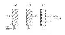
図5に、ヘリカルアンテナまたはローディングアンテナとして用いられる従来のアンテナ用コイル素子の一例を示す。図5で、(a)は絶縁体の外観図であり、(b)は絶縁体にコイルエレメントを組み付けた外観図であり、(c)は(b)の断面図である。図5(a)のごとく、略円柱状の樹脂材からなる絶縁体10の外周面に螺旋状に溝12が設けられる。そして、予め螺旋状に形成された導電線からなるコイルエレメント14が、図5(b)、(c)のごとく、溝12に挿入されるようにして絶縁体10に組み付けられる。このコイルエレメント14の一端側に引き出し部が設けられ、アンテナ給電点または棒状エレメントの接続点などとされる。なお、かかる構成からなるアンテナ用コイル素子は、コイルエレメント14の両端側にそれぞれに引き出し部を設けることで、アンテナの中間部に介装されるアンテナ用コイル素子としても使用できる。
【0003】
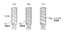
また、図6は、従来のアンテナ用コイル素子の他の一例を示す。図6で、(a)は絶縁体の外観図であり、(b)は絶縁体の外周面全体にメッキにより導電層を設けた外観図であり、(c)は溝以外の導電層を切削除去した外観図である。図6(a)のごとき略円柱状の樹脂材からなる絶縁体10の外周面に、螺旋状に溝12が設けられ、この絶縁体10の外周面全体に、図6(b)のごとく、メッキにより導電層16が施される。そして、この導電層16の溝12以外に付着する部分が切削除去されて、溝12内に螺旋状のコイル状導電層16aが残され、コイルエレメントとして作用する。ここで、樹脂材の表面にメッキを施すには、一般的には、まず無電解メッキにより樹脂材の表面に銅などの導電被膜を形成し、この導電被膜上に電気メッキによりニッケルメッキなどが施される。
【0004】
【発明が解決しようとする課題】
ところで、図5に示すアンテナ用コイル素子にあっては、コイルエレメント14を絶縁体10の溝12に組み付ける際に、コイルエレメント14を弾性変形によりその巻き径を若干拡大させて溝12に挿入しなければならず、その作業が繁雑である。また、コイルエレメント14を絶縁体10の溝12に組み付ける際に、コイルエレメント14の弾性変形を必要以上に行うことで塑性変形を生じさせ易い。かかる塑性変形は、コイルエレメント14の巻き径の変化を生じさせ、アンテナ用コイル素子としてのインダクタンス成分の変化を生じさせ、アンテナ特性が一定にならないこととなる。
【0005】
また、図6に示すアンテナ用コイル素子にあっては、メッキされた導電層16は、硬度が高くしかも薄いために、切削加工時に導電層16が絶縁体10から剥離し易くまたバリを生じさせ易い。そこで、この導電層16の剥離やバリなどにより、やはりアンテナ特性が不安定となり易い。
【0006】
本発明は、かかる従来技術の事情に鑑みてなされたもので、インダクタンス成分が安定していて、量産に好適なアンテナ用コイル素子の製造方法を提供することを目的とする。
【0007】
【課題を解決するための手段】
かかる目的を達成するために、本発明のアンテナ用コイル素子の製造方法は、外周面に螺旋状の溝を設けた絶縁体を金型に挿入し、前記溝内に充填するように熱可塑性の導電性樹脂を射出して、前記溝内に螺旋溝状の前記導電性樹脂によるコイルエレメントを成型する。
【0008】
そして、絶縁体を内周面に螺旋状の溝が設けられた金型に挿入し、前記螺旋状の溝に熱可塑性の導電性樹脂を射出して、前記絶縁体の外周面に螺旋状に前記導電性樹脂によるコイルエレメントを成型しても良い。
【0009】
また、内周面に螺旋状の溝を設けた絶縁体に金型を挿入し、前記溝内に充填するように熱可塑性の導電性樹脂を射出して、前記溝内に螺旋溝状の前記導電性樹脂によるコイルエレメントを成型しても良い。
【0010】
さらに、前記成型された導電性樹脂の表面に電気メッキで導電層を施すことも可能である。
【0011】
【発明の実施の形態】
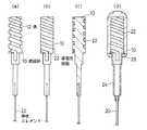
以下、本発明のアンテナ用コイル素子の製造方法の第1実施例を図1を参照して説明する。図1で、(a)は絶縁体の外観図であり、(b)は絶縁体に導電性樹脂を螺旋状に成型した外観図であり、(c)は(b)の断面図であり、(d)は絶縁体および導電性樹脂の上に樹脂キャップを被せた断面図である。
【0012】
図1に示す第1実施例において、略円柱状の樹脂材からなる絶縁体10の外周面に螺旋状の溝12が設けられることは、従来例と同じである。ただ、本発明の実施例にあっては、アンテナ用コイル素子をローディングアンテナとして作用させるべく、絶縁体10の一端部に棒状エレメント20が一体成型により配設固定されている。そして、この絶縁体10が、円柱状の内形を有する金型(図示せず)に挿入されて、図1(b)、(c)のごとく、溝12に導電性樹脂22が射出成型により充填配設されて一体的に成型される。この螺旋状に成型された導電性樹脂22でコイルエレメントが構成される。この導電性樹脂22の素材は、ポリエチレンスルファイト(PPS)やシンジオタクテックポリエチレン(SPS)などの熱可塑性でしかも誘電正接が0.001〜0.002程度で電気的ロスの少ない樹脂材料をベースにして、カーボンファイバーおよび炭素粉末を混入させてその固有抵抗を1〜10オームとしたものである。すると、溝12が螺旋状であるので、導電性樹脂22も帯状でしかも螺旋状に成型され、コイルエレメントとして作用し得る。また、導電性樹脂22が一体的に成型された絶縁体10に、金属スリーブ24が被せられて導電性樹脂22と棒状エレメント20が適宜に電気的接続され、さらに絶縁体10を覆うように樹脂キャップ26が一体成型される。
【0013】
図1に示す本発明のアンテナ用コイル素子の製造方法の第1実施例にあっては、螺旋状に導電性樹脂22が成型されてコイルエレメントが構成されているので、その巻き径やピッチなどが一定であり、アンテナ用コイル素子としてのインダクタンス成分が安定したものである。そこで、アンテナ特性が安定したものとなる。しかも、金型により樹脂を成型するので、成型条件を一定にすることで、容易にかつ安価でしかも安定したアンテナ特性を有するアンテナ用コイル素子を量産するのに好適である。
【0014】
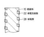
さらに、図2を参照して第1実施例のアンテナ用コイル素子の製造方法を改良した第2実施例につき説明する。図2は、第2実施例の導電性樹脂を一体成型した絶縁体の拡大断面部分図である。図2に示す第2実施例では、導電性樹脂22の表面に導電層28が施されている。螺旋状に一体成型された導電性樹脂22は、もちろん通電が可能であり、無電解メッキを必要とせずに、直接的に電気メッキによりニッケルメッキなどの導電層28を導電性樹脂22の表面に施すことができる。しかも、導電性樹脂22の表面にしかメッキされることがなく、従来のごとく不用な導電層の部分を切削除去する必要がない。この導電層28を施すことにより、コイルエレメントとしての固有抵抗をより小さくでき、信号の損失を少なくすることができる。
【0015】
そして、本発明のアンテナ用コイル素子の製造方法の第3実施例を図3を参照して説明する。図3で、(a)は絶縁体の外観図であり、(b)は絶縁体に導電性樹脂を螺旋状に成型した外観図であり、(c)は(b)の断面図であり、(d)は導電性樹脂に導電層を施した拡大断面部分図である。図3において、図1および図2と同じまたは均等な部材には同じ符号を付けて重複する説明を省略する。
【0016】
図3に示す第3実施例において、図3(a)のごとく、略円柱状の樹脂材からなる絶縁体30の外周面には螺旋状の溝が設けられていない。そして、かかる絶縁体30が、円柱状の内形でその内周面に螺旋状の溝が設けられた金型(図示せず)に挿入されて、図3(b)、(c)のごとく、絶縁体30の外周面に螺旋状に導電性樹脂32が射出成型により絶縁体30と一体的に成型されて、コイルエレメントが構成される。さらに、この導電性樹脂32の表面に電気メッキにより導電層34が施される。
【0017】
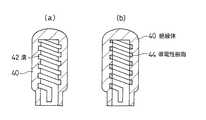
また、本発明のアンテナ用コイル素子の製造方法の第4実施例を図4を参照して説明する。図4で、(a)は筒状の絶縁体の断面図であり、(b)は絶縁体の内周面に導電性樹脂を螺旋状に成型した断面図である。図4に示す第4実施例にあっては、図4(a)のごとく、樹脂キャップのごとく作用する筒状の絶縁体40の内周面に螺旋状の溝42が設けられている。この絶縁体40の内形に金型(図示せず)が挿入され、図4(b)のごとく、溝42に導電性樹脂44が射出成型により充填配設されて一体的に成型され、この導電性樹脂44によりコイルエレメントが構成される。図示していないが、必要であれば、螺旋状の導電性樹脂44の表面に電気メッキにより導電層を施しても良い。
【0018】
かかる第4実施例にあっては、ヘリカルアンテナとして好適であり、しかも樹脂キャップとして作用する絶縁体40に、コイルエレメントとしての導電性樹脂44が一体的に成型されるので、部品点数が少なく、それだけ量産にも好適である。ここで、筒状の絶縁体40の内周面に螺旋状の溝を設けず、金型の構造が複雑になるが、絶縁体40の溝が設けられていない内周面に螺旋状に導電性樹脂を一体的に成型しても良いことは勿論である。
【0019】
なお、上記実施例はいずれもローディングコイルやヘリカルアンテナとして用いるアンテナ用コイル素子の製造方法として説明したが、これに限られず、アンテナ用コイル素子の軸方向両端側に引き出し部を設けて、アンテナの中間部に介装されるアンテナ用コイル素子の製造方法として用いても良い。
【0020】
【発明の効果】
以上説明したように、本発明のアンテナ用コイル素子の製造方法により、以下のごとき格別な効果を奏する。
【0021】
請求項1記載のアンテナ用コイル素子の製造方法は、溝に充填配設されて成型された導電性樹脂でコイルエレメントが構成されるので、インダクタンス成分が変動するようなことがない。そこで、アンテナ特性が安定したものとなる。また、樹脂の金型成型により製造できるので、量産に好適である。
【0022】
そして、請求項2記載のアンテナ用コイル素子の製造方法にあっては、金型成型により螺旋状に配設した導電性樹脂でコイルエレメントが構成されるので、請求項1記載のアンテナ用コイル素子の製造方法と同様の効果がある。しかも、請求項1では絶縁体を成型する金型が複雑で導電性樹脂を成型する金型が比較的に簡単であるが、請求項2では絶縁体を成型する金型は簡単であるが導電性樹脂を成型する金型が複雑なものとなる。
【0023】
また、請求項3記載のアンテナ用コイル素子の製造方法にあっては、絶縁体の内周面に螺旋状に一体成型された導電性樹脂でコイルエレメントが構成されるとともに、絶縁体が樹脂キャップとしても作用するので、それだけアンテナの部品点数を少なくすることが可能である。
【0024】
さらに、請求項4記載のアンテナ用コイル素子の製造方法にあっては、電気メッキにより螺旋状の導電性樹脂の表面に導電層を施すことができ、コイルエレメントの固有抵抗を小さくでき、それだけ信号の損出を少なくすることができる。しかも、メッキによる導電層は導電性樹脂の表面にのみ施され、従来のごとく不要にメッキされた導電層の部分を切削除去するなどの作業を必要とせず、またこの切削による従来例のごとき不具合を生ずることがない。
【0025】
【図面の簡単な説明】
【図1】 本発明のアンテナ用コイル素子の製造方法の第1実施例を示し、(a)は絶縁体の外観図であり、(b)は絶縁体に導電性樹脂を螺旋状に成型した外観図であり、(c)は(b)の断面図であり、(d)は絶縁体および導電性樹脂の上に樹脂キャップを被せた断面図である。
【図2】 本発明のアンテナ用コイル素子の製造方法の第2実施例の導電性樹脂を一体成型した絶縁体の拡大断面部分図である。
【図3】 本発明のアンテナ用コイル素子の製造方法の第3実施例を示し、(a)は絶縁体の外観図であり、(b)は絶縁体に導電性樹脂を螺旋状に成型した外観図であり、(c)は(b)の断面図であり、(d)は導電性樹脂に導電層を施した拡大断面部分図である。
【図4】 本発明のアンテナ用コイル素子の製造方法の第4実施例を示し、(a)は筒状の絶縁体の断面図であり、(b)は絶縁体の内周面に導電性樹脂を螺旋状に成型した断面図である。
【図5】 ヘリカルアンテナまたはローディングアンテナとして用いられる従来のアンテナ用コイル素子の一例を示し、(a)は絶縁体の外観図であり、(b)は絶縁体にコイルエレメントを組み付けた外観図であり、(c)は(b)の断面図である。
【図6】 従来のアンテナ用コイル素子の他の一例を示し、(a)は絶縁体の外観図であり、(b)は絶縁体の外周面全体にメッキにより導電層を設けた外観図であり、(c)は溝以外の導電層を切削除去した外観図である。
【0026】
【符号の説明】
10、30、40 絶縁体
12、42 溝
16、28、34 導電層
22、32、44 導電性樹脂[0001]
BACKGROUND OF THE INVENTION
The present invention relates to amethod of manufacturing an antenna coil element used for an antenna.
[0002]
[Prior art]
FIG. 5 shows an example of a conventional antenna coil element used as a helical antenna or a loading antenna. 5A is an external view of an insulator, FIG. 5B is an external view in which a coil element is assembled to the insulator, and FIG. 5C is a cross-sectional view of FIG. As shown in FIG. 5A, the
[0003]
FIG. 6 shows another example of a conventional antenna coil element. 6A is an external view of the insulator, FIG. 6B is an external view in which a conductive layer is provided on the entire outer peripheral surface of the insulator by plating, and FIG. 6C is a cut of the conductive layer other than the groove. It is the removed external view. As shown in FIG. 6 (b), a
[0004]
[Problems to be solved by the invention]
Incidentally, in the antenna coil element shown in FIG. 5, when the
[0005]
In the antenna coil element shown in FIG. 6, since the plated
[0006]
The present invention has been made in view of the circumstances of the prior art, and an object of the present invention is to provide amethod formanufacturing a coil element for an antenna that has a stable inductance component and is suitable for mass production.
[0007]
[Means for Solving the Problems]
In order to achieve such an object, the antenna coil element manufacturing method of the present invention includes a thermoplastic resin inwhich an insulator having a spiralgroove on its outer peripheral surface is inserted into a mold and filled in the groove. A conductive resin is injected toform a spiral groove-shaped coil element in the groove .
[0008]
Then, theinsulator is inserted into a mold provided with a spiral grooveon the inner peripheral surface, and a thermoplastic conductive resin is injected into the spiral grooveto spiral the outer peripheral surface of the insulator. A coil element made of the conductive resin may be molded.
[0009]
Further, a mold is inserted into aninsulator provided with a spiral groove on the inner peripheral surface, and a thermoplastic conductive resin is injected so as to fill thegroove, and the spiral groove-like shape is injected into thegroove. A coil element made of a conductive resin may be molded.
[0010]
Further, a conductive layer can be applied to the surface of the molded conductive resin by electroplating.
[0011]
DETAILED DESCRIPTION OF THE INVENTION
Hereinafter, a first embodiment of amethod formanufacturing an antenna coil element according tothe present invention will be described with reference to FIG. In FIG. 1, (a) is an external view of an insulator, (b) is an external view in which a conductive resin is molded into a spiral in an insulator, and (c) is a cross-sectional view of (b). (D) is sectional drawing which covered the resin cap on the insulator and conductive resin.
[0012]
In the first embodiment shown in FIG. 1, the
[0013]
In the first embodimentof themethod formanufacturing the antenna coil element of the present invention shown in FIG. 1, the coil element is formed by molding the
[0014]
Further, with reference to FIG. 2, a second embodiment in which the antenna coil elementmanufacturing method of the first embodiment is improved will be described. FIG. 2 is an enlarged partial sectional view of an insulator integrally molded with the conductive resin of the second embodiment. In the second embodiment shown in FIG. 2, a conductive layer 28 is applied to the surface of the
[0015]
A third embodiment of themethod formanufacturing the coil element for antenna according to the present invention will be described with reference to FIG. In FIG. 3, (a) is an external view of an insulator, (b) is an external view in which a conductive resin is molded into a spiral in an insulator, and (c) is a cross-sectional view of (b). (D) is the expanded sectional fragmentary view which gave the conductive layer to conductive resin. In FIG. 3, the same or equivalent members as those in FIGS.
[0016]
In the third embodiment shown in FIG. 3, as shown in FIG. 3A, no spiral groove is provided on the outer peripheral surface of the
[0017]
A fourth embodiment of themethod formanufacturing an antenna coil elementof the present invention will be described with reference to FIG. 4A is a cross-sectional view of a cylindrical insulator, and FIG. 4B is a cross-sectional view of a conductive resin spirally formed on the inner peripheral surface of the insulator. In the fourth embodiment shown in FIG. 4, as shown in FIG. 4A, a
[0018]
In the fourth embodiment, since the conductive resin 44 as the coil element is integrally formed with the
[0019]
In addition, although the said Example demonstrated all asa manufacturing method of the coil element for antennas used as a loading coil or a helical antenna, it is not restricted to this, A drawer | drawing-out part is provided in the axial direction both ends of the coil element for antennas, it may be used as amanufacturing method of an intermediate portionantenna coil element interposed.
[0020]
【The invention's effect】
As described above, themethod formanufacturing an antenna coil elementof the present invention has the following special effects.
[0021]
In themethod for manufacturing a coil element for anantenna according to the first aspect, since the coil element is made of a conductive resin filled and molded in the groove, the inductance component does not fluctuate. Therefore, the antenna characteristics are stable. Moreover, since it can manufacture by resin mold shaping | molding, it is suitable for mass production.
[0022]
In themethod formanufacturing an antenna coil element according to claim 2, the coil element is formed of a conductive resin arranged in a spiral shapeby molding, so that the coil element for antenna according to claim 1 is used.This has the same effect asthe manufacturing method . In addition, in claim 1, the mold for molding the insulator is complicated and the mold for molding the conductive resin is relatively simple. In claim 2, the mold for molding the insulator is simple but conductive. The mold for molding the functional resin becomes complicated.
[0023]
Further, in themanufacturing method of the antenna coil device according to claim 3, wherein, together with the coil element is configured integrally molded conductive resin spirally on the inner circumferential surface of theinsulator, insulator resin cap Therefore, the number of antenna parts can be reduced accordingly.
[0024]
Furthermore, inthe manufacturing method of the coil element for anantenna according to claim 4, the conductive layer can be applied to the surface of the spiral conductive resin by electroplating, the specific resistance of the coil element can be reduced, and the signal is increased accordingly. Can reduce the loss. In addition, the conductive layer formed by plating is applied only to the surface of the conductive resin, so that it is not necessary to perform operations such as cutting and removing the unnecessary portion of the conductive layer that has been plated unnecessarily. Will not occur.
[0025]
[Brief description of the drawings]
1A and 1B show a first embodiment of amethod for manufacturing a coil element for anantenna according to the present invention,wherein FIG. 1A is an external view of an insulator, and FIG. It is an external view, (c) is a cross-sectional view of (b), and (d) is a cross-sectional view in which a resin cap is put on an insulator and a conductive resin.
FIG. 2 is an enlarged partial sectional view of an insulator formed by integrally molding a conductive resin according to a second embodiment of themethod formanufacturing a coil element for an antenna of the present invention.
FIGS. 3A and 3B show a third embodiment of amethod formanufacturing a coil element for an antenna according to the present invention,wherein FIG. 3A is an external view of an insulator, and FIG. 3B is a diagram in which a conductive resin is formed into a spiral in the insulator. It is an external view, (c) is a sectional view of (b), and (d) is an enlarged sectional partial view in which a conductive layer is applied to a conductive resin.
4A and 4B show a fourth embodiment of amethod formanufacturing an antenna coil element according tothe present invention, in which FIG. 4A is a cross-sectional view of a cylindrical insulator, and FIG. It is sectional drawing which shape | molded resin helically.
5A and 5B show an example of a conventional antenna coil element used as a helical antenna or a loading antenna. FIG. 5A is an external view of an insulator, and FIG. 5B is an external view of a coil element assembled to an insulator. (C) is a sectional view of (b).
6A and 6B show another example of a conventional coil element for an antenna, wherein FIG. 6A is an external view of an insulator, and FIG. 6B is an external view in which a conductive layer is provided by plating on the entire outer peripheral surface of the insulator. And (c) is an external view in which a conductive layer other than the groove is removed by cutting.
[0026]
[Explanation of symbols]
10, 30, 40
Claims (4)
Translated fromJapanesePriority Applications (1)
| Application Number | Priority Date | Filing Date | Title |
|---|---|---|---|
| JP36607698AJP4252140B2 (en) | 1998-12-08 | 1998-12-08 | Method for manufacturing antenna coil element |
Applications Claiming Priority (1)
| Application Number | Priority Date | Filing Date | Title |
|---|---|---|---|
| JP36607698AJP4252140B2 (en) | 1998-12-08 | 1998-12-08 | Method for manufacturing antenna coil element |
Publications (2)
| Publication Number | Publication Date |
|---|---|
| JP2000173825A JP2000173825A (en) | 2000-06-23 |
| JP4252140B2true JP4252140B2 (en) | 2009-04-08 |
Family
ID=18485870
Family Applications (1)
| Application Number | Title | Priority Date | Filing Date |
|---|---|---|---|
| JP36607698AExpired - Fee RelatedJP4252140B2 (en) | 1998-12-08 | 1998-12-08 | Method for manufacturing antenna coil element |
Country Status (1)
| Country | Link |
|---|---|
| JP (1) | JP4252140B2 (en) |
Families Citing this family (9)
| Publication number | Priority date | Publication date | Assignee | Title |
|---|---|---|---|---|
| JP2001338812A (en)* | 2000-05-26 | 2001-12-07 | Matsushita Electric Works Ltd | Coil and its manufacturing method |
| CN1181509C (en)* | 2000-09-14 | 2004-12-22 | 松下电工株式会社 | Electromagnetic device, high voltage generator, and method for manufacturing electromagnetic device |
| JP2002280236A (en)* | 2001-03-22 | 2002-09-27 | Matsushita Electric Works Ltd | High-voltage pulse transformer |
| FR2866479A1 (en)* | 2004-02-12 | 2005-08-19 | Thomson Licensing Sa | METHOD FOR MANUFACTURING ANTENNA AND / OR ANTENNA NETWORK, ANTENNA AND / OR ANTENNA NETWORK MANUFACTURED BY SUCH A METHOD |
| WO2006126662A1 (en)* | 2005-05-27 | 2006-11-30 | Namiki Seimitsu Houseki Kabushikikaisha | Tubular coil and tubular micromotor employing it |
| US9130602B2 (en) | 2006-01-18 | 2015-09-08 | Qualcomm Incorporated | Method and apparatus for delivering energy to an electrical or electronic device via a wireless link |
| US9774086B2 (en)* | 2007-03-02 | 2017-09-26 | Qualcomm Incorporated | Wireless power apparatus and methods |
| US9124120B2 (en) | 2007-06-11 | 2015-09-01 | Qualcomm Incorporated | Wireless power system and proximity effects |
| JP5613874B2 (en)* | 2010-07-26 | 2014-10-29 | 並木精密宝石株式会社 | Cylindrical micropattern coil and cylindrical micromotor using the same |
- 1998
- 1998-12-08JPJP36607698Apatent/JP4252140B2/ennot_activeExpired - Fee Related
Also Published As
| Publication number | Publication date |
|---|---|
| JP2000173825A (en) | 2000-06-23 |
Similar Documents
| Publication | Publication Date | Title |
|---|---|---|
| KR100366925B1 (en) | Inductor and method for manufacturing same | |
| US5905475A (en) | Antenna, particularly a mobile phone antenna, and a method to manufacture the antenna | |
| KR100337739B1 (en) | Method of Producing Inductor | |
| US3978581A (en) | Method of making a pin plug | |
| JP6060116B2 (en) | Surface mount inductor and manufacturing method thereof | |
| US6137452A (en) | Double shot antenna | |
| JP4252140B2 (en) | Method for manufacturing antenna coil element | |
| JP2000183626A (en) | Helical antenna molding method | |
| US4255735A (en) | Precision injection-molded coil form | |
| US4086596A (en) | Whip antenna assembly and method of manufacture | |
| US6111554A (en) | Helical antenna element | |
| JP2016042683A (en) | Composite antenna, and manufacturing method thereof | |
| US3815069A (en) | Process for the manufacture of electrical coils | |
| US3243866A (en) | Method of making a miniature slip-ring assembly | |
| WO2001031736A1 (en) | Helical antenna | |
| JP3223366B2 (en) | antenna | |
| JPH10215116A (en) | Antenna element and its manufacture | |
| CN1156938C (en) | Antenna assembly comprising whip antenna and helical antenna contained in antenna top rotatably mounted on top end of whip antenna | |
| JPH11154819A (en) | Small helical antenna | |
| JPH1168436A (en) | Antenna for mobile communication device and method of manufacturing the same | |
| JP3163480B2 (en) | Whip antenna and manufacturing method thereof | |
| JP3469613B2 (en) | Chip coil | |
| JP3179343B2 (en) | Helical antenna and antenna device provided with the helical antenna at the tip | |
| JPH11225012A (en) | Antenna element, its manufacture and radio equipment | |
| JP4153638B2 (en) | Antenna device for portable radio |
Legal Events
| Date | Code | Title | Description |
|---|---|---|---|
| A621 | Written request for application examination | Free format text:JAPANESE INTERMEDIATE CODE: A621 Effective date:20051115 | |
| A977 | Report on retrieval | Free format text:JAPANESE INTERMEDIATE CODE: A971007 Effective date:20080626 | |
| A131 | Notification of reasons for refusal | Free format text:JAPANESE INTERMEDIATE CODE: A131 Effective date:20080708 | |
| A521 | Written amendment | Free format text:JAPANESE INTERMEDIATE CODE: A523 Effective date:20080904 | |
| A131 | Notification of reasons for refusal | Free format text:JAPANESE INTERMEDIATE CODE: A131 Effective date:20081007 | |
| A521 | Written amendment | Free format text:JAPANESE INTERMEDIATE CODE: A523 Effective date:20081127 | |
| TRDD | Decision of grant or rejection written | ||
| A01 | Written decision to grant a patent or to grant a registration (utility model) | Free format text:JAPANESE INTERMEDIATE CODE: A01 Effective date:20090120 | |
| A01 | Written decision to grant a patent or to grant a registration (utility model) | Free format text:JAPANESE INTERMEDIATE CODE: A01 | |
| A61 | First payment of annual fees (during grant procedure) | Free format text:JAPANESE INTERMEDIATE CODE: A61 Effective date:20090121 | |
| R150 | Certificate of patent or registration of utility model | Free format text:JAPANESE INTERMEDIATE CODE: R150 | |
| FPAY | Renewal fee payment (event date is renewal date of database) | Free format text:PAYMENT UNTIL: 20120130 Year of fee payment:3 | |
| LAPS | Cancellation because of no payment of annual fees |