JP4251664B2 - Biomaterial - Google Patents
BiomaterialDownload PDFInfo
- Publication number
- JP4251664B2 JP4251664B2JP50821497AJP50821497AJP4251664B2JP 4251664 B2JP4251664 B2JP 4251664B2JP 50821497 AJP50821497 AJP 50821497AJP 50821497 AJP50821497 AJP 50821497AJP 4251664 B2JP4251664 B2JP 4251664B2
- Authority
- JP
- Japan
- Prior art keywords
- silicon
- bioactive
- porous
- apatite
- wafer
- Prior art date
- Legal status (The legal status is an assumption and is not a legal conclusion. Google has not performed a legal analysis and makes no representation as to the accuracy of the status listed.)
- Expired - Lifetime
Links
Images


Classifications
- A—HUMAN NECESSITIES
- A61—MEDICAL OR VETERINARY SCIENCE; HYGIENE
- A61L—METHODS OR APPARATUS FOR STERILISING MATERIALS OR OBJECTS IN GENERAL; DISINFECTION, STERILISATION OR DEODORISATION OF AIR; CHEMICAL ASPECTS OF BANDAGES, DRESSINGS, ABSORBENT PADS OR SURGICAL ARTICLES; MATERIALS FOR BANDAGES, DRESSINGS, ABSORBENT PADS OR SURGICAL ARTICLES
- A61L27/00—Materials for grafts or prostheses or for coating grafts or prostheses
- A61L27/28—Materials for coating prostheses
- A61L27/30—Inorganic materials
- A61L27/306—Other specific inorganic materials not covered by A61L27/303 - A61L27/32
- A—HUMAN NECESSITIES
- A61—MEDICAL OR VETERINARY SCIENCE; HYGIENE
- A61L—METHODS OR APPARATUS FOR STERILISING MATERIALS OR OBJECTS IN GENERAL; DISINFECTION, STERILISATION OR DEODORISATION OF AIR; CHEMICAL ASPECTS OF BANDAGES, DRESSINGS, ABSORBENT PADS OR SURGICAL ARTICLES; MATERIALS FOR BANDAGES, DRESSINGS, ABSORBENT PADS OR SURGICAL ARTICLES
- A61L27/00—Materials for grafts or prostheses or for coating grafts or prostheses
- A61L27/02—Inorganic materials
- A61L27/025—Other specific inorganic materials not covered by A61L27/04 - A61L27/12
- A—HUMAN NECESSITIES
- A61—MEDICAL OR VETERINARY SCIENCE; HYGIENE
- A61L—METHODS OR APPARATUS FOR STERILISING MATERIALS OR OBJECTS IN GENERAL; DISINFECTION, STERILISATION OR DEODORISATION OF AIR; CHEMICAL ASPECTS OF BANDAGES, DRESSINGS, ABSORBENT PADS OR SURGICAL ARTICLES; MATERIALS FOR BANDAGES, DRESSINGS, ABSORBENT PADS OR SURGICAL ARTICLES
- A61L27/00—Materials for grafts or prostheses or for coating grafts or prostheses
- A61L27/28—Materials for coating prostheses
- A61L27/30—Inorganic materials
- A61L27/32—Phosphorus-containing materials, e.g. apatite
- A—HUMAN NECESSITIES
- A61—MEDICAL OR VETERINARY SCIENCE; HYGIENE
- A61L—METHODS OR APPARATUS FOR STERILISING MATERIALS OR OBJECTS IN GENERAL; DISINFECTION, STERILISATION OR DEODORISATION OF AIR; CHEMICAL ASPECTS OF BANDAGES, DRESSINGS, ABSORBENT PADS OR SURGICAL ARTICLES; MATERIALS FOR BANDAGES, DRESSINGS, ABSORBENT PADS OR SURGICAL ARTICLES
- A61L27/00—Materials for grafts or prostheses or for coating grafts or prostheses
- A61L27/50—Materials characterised by their function or physical properties, e.g. injectable or lubricating compositions, shape-memory materials, surface modified materials
- A61L27/56—Porous materials, e.g. foams or sponges
- A—HUMAN NECESSITIES
- A61—MEDICAL OR VETERINARY SCIENCE; HYGIENE
- A61F—FILTERS IMPLANTABLE INTO BLOOD VESSELS; PROSTHESES; DEVICES PROVIDING PATENCY TO, OR PREVENTING COLLAPSING OF, TUBULAR STRUCTURES OF THE BODY, e.g. STENTS; ORTHOPAEDIC, NURSING OR CONTRACEPTIVE DEVICES; FOMENTATION; TREATMENT OR PROTECTION OF EYES OR EARS; BANDAGES, DRESSINGS OR ABSORBENT PADS; FIRST-AID KITS
- A61F2310/00—Prostheses classified in A61F2/28 or A61F2/30 - A61F2/44 being constructed from or coated with a particular material
- A61F2310/00389—The prosthesis being coated or covered with a particular material
- A61F2310/00592—Coating or prosthesis-covering structure made of ceramics or of ceramic-like compounds
- A61F2310/00598—Coating or prosthesis-covering structure made of compounds based on metal oxides or hydroxides
- A61F2310/0061—Coating made of silicon oxide or hydroxides
- A—HUMAN NECESSITIES
- A61—MEDICAL OR VETERINARY SCIENCE; HYGIENE
- A61F—FILTERS IMPLANTABLE INTO BLOOD VESSELS; PROSTHESES; DEVICES PROVIDING PATENCY TO, OR PREVENTING COLLAPSING OF, TUBULAR STRUCTURES OF THE BODY, e.g. STENTS; ORTHOPAEDIC, NURSING OR CONTRACEPTIVE DEVICES; FOMENTATION; TREATMENT OR PROTECTION OF EYES OR EARS; BANDAGES, DRESSINGS OR ABSORBENT PADS; FIRST-AID KITS
- A61F2310/00—Prostheses classified in A61F2/28 or A61F2/30 - A61F2/44 being constructed from or coated with a particular material
- A61F2310/00389—The prosthesis being coated or covered with a particular material
- A61F2310/00592—Coating or prosthesis-covering structure made of ceramics or of ceramic-like compounds
- A61F2310/00796—Coating or prosthesis-covering structure made of a phosphorus-containing compound, e.g. hydroxy(l)apatite
Landscapes
- Health & Medical Sciences (AREA)
- Chemical & Material Sciences (AREA)
- Life Sciences & Earth Sciences (AREA)
- Animal Behavior & Ethology (AREA)
- Medicinal Chemistry (AREA)
- Oral & Maxillofacial Surgery (AREA)
- Transplantation (AREA)
- Epidemiology (AREA)
- Veterinary Medicine (AREA)
- Dermatology (AREA)
- General Health & Medical Sciences (AREA)
- Public Health (AREA)
- Inorganic Chemistry (AREA)
- Dispersion Chemistry (AREA)
- Materials For Medical Uses (AREA)
- Silicon Compounds (AREA)
Description
Translated fromJapanese本発明は生体用材料に関する。
「生体用材料」とは、生物系と相互作用させることを意図した医療用具において用いられる非生体的材料である。かかる材料は、それらのin vivoでの生体反応に依存して比較的「生物不活性」、「生物適合性」、「生物活性」あるいは「再吸収性」でありうる。
生物活性材料は、各々が、in vivoで生体組織と該物質間の結合形成を生じさせる特異的生体反応を誘発する材料の類である。生物活性材料はまた表面反応性生体用材料とも称される。生体用材料は、生体内への移植に適した物質と定義することもできる。L.L.HenchはScience、208巻、1980年5月、p.826−831に発表された学術論文の中で生体用材料を検討した。比較的不活性な生体用材料は移植した時にインターフェイスの問題を引き起こすことがあり、そのため生体用材料−組織インターフェイスを改善するべく生物活性的である材料の開発に向けて多大な研究活動が行われてきた。
既知の生物活性材料は、ヒドロキシアパタイト(水酸化リン灰石)(HA)、一部のガラスおよび一部のガラスセラミックを含む。生物活性ガラスおよび生物活性ガラスセラミックはいずれも、移植した時生物学的に活性なヒドロキシカルボネートアパタイト(HCA)の層を形成する。この層は化学的および構造的に骨中の無機質相に等しく、骨と生物活性材料間の界面結合の原因となる。これらの生物活性材料の特性は、Journal of the American Ceramic Society、74巻、第7号、1991、p.1487−1510においてL.L.Henchにより記述されている。生物活性材料に関する学術文献はしばしばHAとHCAという用語を交換可能なベースで用いている。本特許明細書においては、HAとHCA材料は集合的にアパタイトと称する。
Lieらは,Journal of Biomedical Materials Reserach、28巻、1994、p.7−15においてシリカゲルへのアパタイトの沈着を報告した。彼らは、ヒドロキシアパタイトの異種核形成を引き起こすためには一定の密度のシラノール(SiOH)基が必要であることを示唆している。シリカガラスサンプルの表面にはアパタイト層は発生せず、これはシリカゲルに比べて表面シラノール基の密度が低いためであると考えられる。
WangらがJournal of Materials Science:Materials in Medicine、6巻、1995、p.94−104の中で述べているように、36℃の生理溶液に浸したアパタイトおよびケイ灰石含有のガラスのプレートのすぐ近くにシリコン単結晶ウェハーを置くことにより、あらかじめアパタイトの厚い被膜をウェハーに沈着させた。擬似体液(SBF)としても知られる生理溶液は人体において認められるものと同様のイオン濃度を含有する溶液であり、生物活性のin vitro試験で身体の反応を擬態するために広く用いられる。Wangらは、(111)Siウェハー上でのアパタイトの生長を報告したが、(100)Siウェハーでは「ほとんど全く」アパタイトが成長できないことも報告している。シリコンウェハー自体は生物活性ではない。Wangらは、「基質上のSi原子がアパタイト核中の酸素原子と強く結合して低エネルギーでインターフェイスを形成することができることを除いて、Siはアパタイト被膜の生長において特別な役割を果たさない。」と述べている。アパタイトの沈着を誘発するためにはアパタイトとケイ灰石を含有するガラスの存在が必要である。実際に、Y.AbeらがJournal of Materials Science:Materials in Medicine、1巻、1990、p.233−238において報告したように、生物活性材料を用いてもうひとつ別の材料を処理する、このいわゆる「生体模倣過程」は様々な生物不活性材料上でのアパタイトの生長を誘発することが示されている。
診断と治療の両方の目的のために人体内でシリコンベースの集積回路を用いる能力が長い間待望されている。シリコンは血液中で低い生物適合性を示すことがKandaらによりElectronics Letters、17巻、第16号、1981、p.558、559の中で報告されており、現在、集積回路を生体環境での損傷から保護するために適切な材料による被包が必要である。シリコンベースのセンサーの医療応用がJournal of Physics E:Sci.Instrum.、16巻、1983、p.987−994の中のEngelsらの論文において記述されている。
本発明は、シリコンが少なくとも部分的に結晶性であることを特徴とする生物活性シリコンを提供する。
生物活性シリコンは、他の生物活性材料に比べて、シリコンベースの集積回路テクノロジーと適合性があるという利点を提供する。また非生物活性シリコンに比べてより大きな生物適合性を示すという利点を持つ。さらに、生物活性シリコンは生きている動物の骨あるいは血管組織への結合を形成するために使用することができる。生物活性シリコンは、小型化包装適用における包装材料としての使用に適した材料を提供しうる。
シリコンの生物活性特性は、生理的温度の擬似体液中に材料を液浸することによって証明され、かかる液浸は生物活性シリコンへの材料の沈着を生じさせる。無機質沈着物はアパタイトであってもよい。アパタイト沈着物は100μm2より広い面積にわたって連続的でありうる。生物活性シリコンは少なくとも部分的には有孔シリコンである。有孔シリコンは4%より多く、70%未満の有孔性を持ちうる。
バルクの結晶性シリコンは、米国特許第5,348,618号に述べられているように、フッ化水素酸ベースの溶液中での部分的な電気化学的溶解によって多孔化することができる。このエッチング工程に、最初のバルク材料の結晶性と結晶学的方向性を保持するシリコン構造を生じる。このようにして形成された多孔性シリコンは、結晶性シリコンの形態である。低レベルの、たとえば20%以下の有孔性では、有孔シリコンの電子特性はバルク結晶性シリコンの電子特性に類似している。
有孔シリコンはその有孔性に従って再分することができる。微小孔性シリコンは直径20Å未満の孔を含む;中孔性シリコンは直径が20Åから500Åまでの範囲の孔を含む;大孔性シリコンは直径500Åより大きい孔を含む。生物活性シリコンは微小孔性あるいは中孔性のいずれかの有孔シリコンから成る。
シリコンは、数多くの金属、セラミックおよびポリマーとは対照的に、有望な生体用材料と評価されたことは一度もなく、また生物活性反応を示すことができるとも考えられてこなかった。実際に、半導体が生物活性であると報告されたことはない。シリコンはせいぜい、比較的生物不活性であるが概して低い生物適合性を示すと報告されている。集積回路の小型化においてもたらされた進歩にもかかわらず、シリコンのVLSIテクノロジーは、N.G.Einspruchらが編集した「VLSI in Medicine」、Academic Press,New York,1989、第10章の中でK.W.Wiseらによって、またAppl.Biochem.Biotechn.,41巻、1993、p.109−128の中でM.Madouらによって述べられているように、まだ観血的医療適用およびバイオセンサー適用のための開発下にある。
生物学的適用のためのシリコン構造の使用は知られている。国際出願番号第WO95/24472を持つ国際特許願第PCT/US95/025752号は、有孔非晶質シリコン構造から形成されるエンドフェイスを持つカプセルを記述しており、その孔は、所望する分子産物は通過させるがより大きな免疫学的分子の通過は遮断するのに十分な大きさであり、カプセルの中に含まれている細胞の免疫学的分離を提供する。シリコン構造の生物適合性に関する証拠は示されておらず、生物適合性材料の分野の当業者は、かかる装置がin vivoでは孔を閉塞する線維組織の産生を刺激することを予測するであろう。IEEE Transactions on Biomedical Engineering、39巻、第6号、1992、p.635においてD.J.Edellらが報告したように、微小機械化されたシリコン構造を神経要素のためのセンサーとして使用する時、シリコン表面と対象とする神経要素の間に線維組織の層が形成されることが知られている。実際に、形成される線維組織層の厚さと特性がしばしば生物適合性のひとつの基準として使用され、層が薄いほど含まれる細胞壊死が少なく、より高い生物適合性を反映する。
米国特許第5,225,374号は、in vitro溶液中で標的種に接触させた時、標的種と相互作用して電流を生じさせるたんぱく−脂質被膜のための基質としての有孔シリコンの使用を記述している。有孔シリコンは酸化されて親水性表面を生じ、またその孔がイオン流動のための導管として働き、その構造が脂質層のための構造的支持体を提供することから選択されている。該有孔シリコンはたんぱく−脂質被膜によってin vitro溶液から分離されており、そのため有孔シリコンの生物活性あるいは生物適合性の問題は起きてこない。
有孔シリコンは、M.ThustらによりMeas.Sci.Technol.、7巻、1996、p.26−29においてin vitroバイオセンサーのための基質材料として提案された。その中に述べられている装置の構造では、有孔シリコンを熱酸化工程に供して、孔の露出したシリコン表面上に二酸化ケイ素の層を形成させる。有孔シリコンは部分的に熱酸化されるので、被検液に接触するのは二酸化ケイ素だけであるため、シリコンの生物活性あるいは生物適合性は問題とならない。有孔シリコンは、酵素溶液のための有効な不活性宿主である。
E.RichterらによりJournal of Materials Science:Materials in Medicine、7巻、1996、p.85−97において、またG.FuhrらによりJournal of Micromechanics and Microengineering、5巻、第2号、1995、p.77−85において、微小穿孔したシリコン膜は細胞構造を支持することができると述べられている。その中に述べられているシリコン膜は、リソグラフィ工程を用いて幅5μm〜20μmの正方形の孔によって穿孔した厚さ3μmのシリコン膜を含む。マウスの胚線維芽細胞は清浄にした膜上で増殖することができたが、膜をポリリシンで被覆すると細胞の付着が改善された。この論文はシリコン膜の生物活性に関しては触れておらず、細胞培地に接触させた時に形成されるアパタイト層についても言及していない。実際に、使用されている孔の大きさを考慮すると、該構造は重要な度合の生物活性を示しそうにない。さらに、依然として長期的安定性を備えた細胞適合性材料を発見し、開発する必要があることがFuhrらによって認められている。
Journal of Vacuum Science Technology A、13巻、第5号、1995、p.2608−2612においてA.Offenhausserらは、基質を超薄ポリマーフィルムで被覆することによってシリコン基質との生物適合性を実現するための手法を記述している。同様に、R.S.PotemberらはProc.第16回国際会議、IEEE Engineering in Medicine and Biology Society、2巻、1994、p.842−843において、ラットのニューロンの発達を促進するための、シリコン表面に付着させた合成ペプチドの使用を記述している。
もうひとつの側面では、本発明はシリコンが少なくとも部分的に結晶性であることを特徴とする生物活性なシリコン構造を提供する。
さらにもうひとつの側面では、本発明は、装置が生物活性シリコンを含むことを特徴とする、生きているヒトあるいは動物の体内での操作のための電子装置を提供する。
本発明の生物活性シリコンは、電子回路のための保護的被膜として、ならびに装置を骨あるいは他の組織に付着させるための手段として配置される。
電子装置は、センサー装置あるいは知的薬剤供給送達のための装置あるいはプロテーゼ装置でありうる。
さらにもうひとつの側面では、本発明はシリコンを生物活性にする方法を提供し、かかる方法はシリコンの少なくとも一部を有孔にすることを含む。
もうひとつの側面では、本発明は、多結晶性シリコンの層を沈着させる段階を含むことを特徴とする、生物活性シリコンの製造方法を提供する。
さらに別の側面では、本発明はシリコンが少なくとも部分的に結晶性であることを特徴とする生物適合性シリコンを提供する。
さらにまた別の側面では、本発明は再吸収性シリコンを提供する。
もうひとつの側面では、本発明は生理的電解質中での無機沈着物のシリコンへの沈着速度を加速あるいは遅延させる方法を提供し、かかる方法はシリコンへの電気バイアスの適用を含む。
該シリコンは有孔シリコンでありうる。
さらなる側面では、本発明は、材料の生物活性が該材料への電気バイアスの適用によって制御できることを特徴とする生物活性材料を提供する。
従来の生物活性セラミックは電気的に絶縁されており、従って電気化学的適用における使用はあらかじめ排除されている。以前に組織成長の電気刺激が検討されたが、電場の直接の作用と移植した「生物不活性」電極付近の生体化学の変化に関連する影響とを識別することがしばしば困難であった。
さらに別の側面では、本発明は、シリコン領域が少なくとも部分的に結晶性であるシリコンを含むことを特徴とする、生物活性シリコン領域とその上の無機沈着物から成る複合構造を提供する。
本発明の考えられる適用は、生物学的検定を実施するための基質としてである。動物の生体での試験に頼らずに、薬物化合物に関して一定の試験が実施できることは望ましい。それ故、基質上に細胞系を支持して、該細胞系への薬物化合物の作用を監視するin vitro試験を開発することに多大の研究努力が注がれてきた。シリコンとアパタイトの複合構造はかかる試験のための適切な基質を提供する。
さらなる側面では、本発明は、生物活性シリコンとその上の無機沈着物から成る複合構造を形成する段階を含むことを特徴とする、バイオセンサーの製造方法を提供する。
本発明はさらに、シリコン基質の少なくとも一部が生物活性シリコンから成ることを特徴とする、化合物の薬理活性を試験するためのシリコン基質を含むバイオセンサーを提供する。
本発明をより十分に理解できるように、単なる例証として、添付の図表を参照しながら以下にその具体例を述べる:
図1は生物活性シリコンウェハーの図式的な断面図である;
図2は、図1のウェハーの有孔領域に隣接するバルクシリコン領域上のアパタイト沈着物の走査型電子顕微鏡(SEM)写真の像である;
図3は、図2のシリコン領域の横断面のSEM写真の像である;
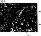
図4は、有孔性31%の有孔シリコン領域上に沈着したアパタイト球状体を示すSEM写真の像である;
図5aは、擬似体液中に液浸した後48%の有孔性を生じるように陽極化したシリコンウェハーの、陽極化していない領域のSEM写真の像である;
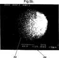
図5bは、図5aのウェハーの陽極化した領域のSEM写真の像である;
図6は生物活性シリコンを包含するバイオセンサーの図式的な概要図である;
図7は生物活性の電気的制御のための電気化学的セルの図式的概要図である;
図8は、図7のセルで処理した後の有孔シリコンウェハー中のカルシウム濃度のプロフィールの図表である;
図9は、本発明の生物活性多結晶性シリコンを包含するバイオセンサー装置の図式的概要図である。
図1を参照すると、通常10で指示される、生物活性シリコンウェハーの断面が示されている。シリコンウェハー10は、有孔領域20と非有孔バルクシリコン領域22から成る。有孔領域20は13.7μmの厚さdと18%の平均有孔性を持つ。シリコンウェハー10は3インチあるいは75mmの直径lを持つ。有孔領域20は67m2/g-1の材料の単位質量当り表面積を持つ。これは、S.J.GreggとK.S.W.Singにより「Adsorbption,Surface Area and Porosity」第2版、Academic Press、1982に述べられているように、BETガス分析手法を用いて測定した。
ウェハー10は、0.012Ωcmの初期抵抗性を持つ、強くヒ素ドープしたCzochralski−grown(CZ)n型(100)シリコンウェハーの陽極化によって製造した。陽極化は、米国特許第5,348,618号に述べられているように、50重量%の水性HFの電解質を含む電気化学的セルにおいて実施した。100mA/cm-2の陽極化電流密度を1分間使用してウェハーを陽極化した。ウェハーの外側付近の合成ゴムワッシャーにより、ウェハーを電気化学的セル中の適当な位置に保持した。その結果として、ウェハーの外側の環は陽極化工程後も陽極化されないままであった。この外側の陽極化されない環が、図1の中で非有孔バルクシリコン領域22として示されている。陽極化されない環は4mmの幅sを持つ。
陽極化されたウェハーの生物活性を測定するために、分割したウェハーの断片を2時間から6週間までの期間擬似体液(SBF)中に入れた。SBF溶液は試薬グレードの塩を脱イオン水に溶解して調製した。該溶液はヒト血漿中で認められるのと同様のイオン濃度を含有した。SBF溶液とヒト血漿のイオン濃度を表1に示す。SBF溶液は、トリヒドロキシメチルアミノメタンと塩酸により、生理的pHに等しい7.30±0.05のpHで有機的に緩衝した。有孔ウェハーをSBF溶液に液浸する前に少なくとも数ヵ月間環境空気中で保存し、それ故有孔シリコンウェハーは水和された。従って有孔シリコンは、空気中での保存の結果バルクシリコン上に形成されるものと同様の、薄い未変性酸化物で被覆されたシリコン骨格を含んだ。
既知の期間後、断片をSBF溶液から取り出し、脱イオン水で洗浄して、環境空気中で乾燥させた後、特性指摘した。走査型電子顕微鏡(SEM)とJEOL6400F顕微鏡でのx線微量分析(EDX)を用いてSBF処理した断片を検討した。Cameca4F機器を用いて二次イオン質量分析を実施し、Biorad FTS−40スペクトロメータを用いて赤外分光測定を実施した。
2、4および17時間のSBF溶液での液浸期間後、有孔シリコン領域20と非有孔バルクシリコン領域22の両方に無視しうるアパタイトの沈着物が生じた。
図2を参照すると、通常50で指示される、SEM顕微鏡写真の再現が示されている。顕微鏡写真50は、ウェハー10を6日間SBF溶液中に入れておいた後の領域20の部分の画像である。秤の棒線52は2μmの寸法を表わす。顕微鏡写真50は、領域22の表面をおおうアパタイト球状体54の連続的な層を示している。アパタイト球状体は、比較的なめらかな被膜を創造するのに十分な高密度で核形成されており、境界56のような球状体間の境界は不明瞭である。被膜は少なくとも100μm2の面積にわたって連続的であった。
図3を参照すると、通常100で指示される、ウェハーをSBF溶液に6日間液浸した後の領域2におけるウェハー10の横断面のSEM顕微鏡写真の再現が示されている。秤の棒線102は1.0μmの寸法を表わす。顕微鏡写真100はA、B、Cの文字で指示される3つの異なる領域を示す。EDX分析により、領域Aが、原材料である非有孔バルクシリコン領域22に相当するシリコンであることを確認した。領域BはEDX分析下でシリコンと酸素の両方のピークを示し、領域Bが酸化シリコンを含むことを示唆した。領域CはEDX分析下でカルシウム、リンおよび酸素のピークを示し、この領域がアパタイトの球状体を含むことと一致した。SEMとEDX分析を組み合わせると、有孔酸化シリコン層(領域B)がバルクシリコン(領域A)上に形成され、それによってアパタイト(領域C)の核形成と被覆が可能になることを明らかにした。
SBF溶液に6日間液浸した後の有孔シリコン領域20の部分におけるウェハー10のSEM分析は領域22に比べてはるかに低いレベルのアパタイト被覆を示した。有孔シリコン領域20は高いレベルの中孔性を有する。SBF溶液に10日間液浸した後、その間に有孔シリコンの重要な層侵食が生じたが、領域20ではSEM分析下で大孔が見えた。SEMとEDX分析を組み合わせると、バルクシリコン領域22と異なって、有孔シリコン領域20では直接アパタイトの核形成が起こり、中間の有孔酸化シリコン層の形成を必要としないことが明らかになった。非常に大きな(直径100μm以上)大孔の意図的な導入は、有孔シリコンの構造内で血管組織を成長させることができるという点で有利でありうる。
アパタイト沈着物の形成は、有孔シリコンの有孔性が18%以外であるウェハーに関しても認められた。有孔性31%の有孔シリコン領域を持つ微小孔ウェハーを、0.03Ωcmの強くホウ素ドープしたp型CZシリコンウェハーから、50重量%HF中で1分間、100mA/cm2の陽極化電流密度で陽極化することによって製造した。生じた有孔シリコン領域は9.4μmの厚さと250m2/gの単位質量当り表面積を有していた。該有孔シリコンウェハーは、相当な期間を経過した後SBF溶液に液浸した。
図4は、通常150で指示される、ウェハー断片を30cm3のSBF溶液に7日間液浸した後の、有孔性31%の有孔シリコン層の表面のSEM顕微鏡写真の像を示す。顕微鏡写真150は、有孔シリコンの表面154上にアパタイトの球状体152などの球状体を示す。
有孔性48%の有孔シリコン領域を持つ微小孔ウェハーを、30Ωcmの抵抗性を持つ軽くホウ素ドープしたp型シリコンウェハーを、50重量%のHF中20mA/cm2の陽極化電流密度で5分間陽極化することによって製造した。生じた有孔シリコン領域は、6.65μmの厚さと約800m2/gの単位質量当り表面積を有していた。該有孔シリコンウェハー断片は、相当な期間を経過した後SBF溶液を満たした150cm3のポリエチレン製ビンに液浸した。
図5aは、通常200で指示される、4週間の液浸期間後の、有孔性48%の非陽極化領域上のアパタイト沈着物202のSEM顕微鏡写真の像を示す。図5bは、通常250で指示される、有孔性48%の有孔領域上に沈着したアパタイト球状体252のSEM顕微鏡写真の像を示す。球状体252は、P.LiらがJournal of Biomedical Materials Research、28巻、p.7−15、1994において述べているように、生物活性セラミック上でアパタイト成長の円柱状構造特性を備えた形態を示す。同様の形態を持つアパタイト球状体がウェハーの非陽極化領域で認められた。非陽極化領域を越えて採取した、SBF溶液で液浸した後の有孔性48%のウェハーの横断面EDXスペクトルは、球状体がアパタイトに一致するカルシウム、リンおよび酸素を含有することを示した。球状体から離れたところに、主としてシリコンと酸素から成る厚さわずか150nmのインターフェイス層が観察された。フーリエ変換赤外分光法は、有孔領域と非有孔領域の両方においてアパタイトの存在を確認する。約600/cmの波数のPO4四面体のP−O屈曲振動モードと、カルボネート基の振動モードに帰せられる約1400/cmの広域バンドの両方が観察された。
一部の形態の有孔シリコンは光輝性であることが知られている。有孔シリコンから赤あるいは橙の光輝が認められることは、一般にシリコン材料の量子ワイヤあるいは量子ドットの存在を示す。SBF溶液に液浸する前に相当な期間を経過した有孔性48%のウェハーは光輝を示し、環境空気との接触により水和されているにもかかわらず、有孔シリコン領域が高濃度の量子ワイヤあるいはドットを保持していることを示唆した。SBF溶液での液浸中および液浸後も発光特性は保存された。これは、アパタイトが発光特性を保存するように有孔シリコン上に沈着することを示す。アパタイト層成長後の発光特性の保存は、電気光学的バイオセンサーの開発にとって有用な特性であると考えられる。
有孔性70%、単位質量当り表面積640m2/g、厚さ1μmの有孔領域を持つ、完全に中孔性の発光性有孔シリコンウェハーをSBF溶液中に入れた。およそ1日後、有孔領域はSBF溶液に溶解して完全に除去されており、ウェハーはもはや発光性ではなかった。有孔シリコン領域あるいは非有孔領域のいずれにもアパタイト沈着物は認められなかった。中孔シリコンはSBF溶液によってより有効に水和され、従って中孔シリコンは微小孔シリコンよりも溶解率が高いと考えられる。それ故中孔シリコンは再吸収性生体用材料特性を示す。可溶性シリコンの供給源として作用する、限られた面積の中孔性シリコンを持つ生物活性シリコン構造を構築することが可能であると考えられる。これは局所的に飽和されたシリコン溶液を生じさせ、従ってアパタイト沈着を促進させることができるであろう。
有孔性4%、厚さ38μmの有孔領域を持つ大孔シリコンウェハーは、SBF溶液に4週間液浸した時、アパタイト沈着物の成長を示さない程度に、バルクの陽極化していないシリコンウェハーと同様に行動した。さらに、有孔性80%、厚さ50μmの有孔シリコン領域ではアパタイトの成長は認められなかったが、この領域はSBF溶液に2週間液浸した後もその発光特性を保持する。
さらなる対照として、有孔シリコンウェハー断片と同様の寸法の、分割した非有孔シリコンウェハー断片を30cm3のSBF溶液中に入れた。SBF溶液に5週間液浸した後、5000/cm2以下の極めて低密度のミクロンサイズの沈着物を認めた。これらの沈着物はおそらくシリコンウェハーの表面欠陥部位に位置していた。従ってバルクの非有孔シリコンは生物活性ではない。生体組織と結合を形成するにはアパタイト沈着物の成長速度が遅すぎるからである。
このようにこれらの実験は、孔の大きさと有孔性を適切に制御することにより、シリコン構造は実質的に生物活性スペクトル全体をカバーできることを示唆している。バルクの純粋に大孔性のシリコンは比較的生物不活性である;有孔性の高い中孔シリコンは再吸収性であり、中等度の有孔性の微小孔シリコンは生物活性である。
生体用材料の化学組成の変化も、それらが生物不活性、再吸収性あるいは生物活性であるかどうかに影響しうることが知られている。シリコンの半導体特性を制御するための夾雑物ドーピング以外には意図的に特異的要素でドープしなかった有孔シリコンウェハーに関して、上記の実験を実施した。SiO2、Na2O、CaOおよびP2O5を含有する生物活性ガラスからのカルシウムの溶出は、局所的過飽和を促進することによってアパタイトの成長を有意に助けると考えられる。40%水性HF中20mA/cm2で1分間陽極化することにより、軽度にドープしたp型(30Ωcm)CZシリコンウェハーにおいて形成される有孔性55%、厚さ1.2μmの微小孔シリコンの新鮮腐食層にカルシウムを透浸させた。カルシウム透浸は、125cm3の純粋エタノール中に5gのCaCl.2H2Oを含有する溶液中で保存することによる軽度の酸化を通して実施した。カルシウム、ナトリウムあるいはリンあるいはこれらの種の組合せによる有孔シリコンの透浸はシリコン上でのアパタイトの形成を促進すると考えられる。
SBF溶液での液浸後、陽極化したウェハーの有孔シリコン領域に隣接する非有孔領域において、アパタイト沈着物の下に酸化シリコン層が存在することは、有孔シリコン領域からのシリコンの溶解が有孔シリコンの生物活性にとって重要な因子であることを示唆している。シリコンの溶解は局所的過飽和溶液を形成し、それが有孔酸化シリコン層の沈着を生じさせると考えられる。その後アパタイトが有孔酸化シリコン上に沈着する。これは、SBF溶液中で通常のバルク結晶性シリコンより高い可溶性を持ち、透浸したカルシウムを含有する、様々な非有孔結晶性、多結晶性あるいは非晶質シリコンをベースとする構造が生物活性であることを示唆している。アパタイトの成長を有意に助けるためには、必ずしもシリコンの結晶性が保存されている必要はないが、カルシウム透浸のレベルが、以前に報告されているカルシウムドープしたシリコンよりもはるかに高いことが必要である。
カルシウムは一般にシリコンにとってあまり魅力的でないドーパントとみなされており、その結果カルシウムドープしたシリコンについての試験はほとんどなかった。Journal of the Electrochemical Society、129巻、1982、p.2809−2812においてSigmundは、単結晶性シリコンにおけるカルシウムの最大平衡溶解度は6.0×10¹⁸/cm3であると報告している。この濃度で、カルシウムはアパタイトの成長に重要な影響を及ぼさないと考えられる。1021/cm3(2%)を越える濃度の、過飽和レベルのカルシウムが必要である。かかる非常な高濃度は次の工程によって達成しうる:
(a)先に述べたような有孔シリコンの溶液ドーピング;
(b)カルシウムイオンによる有孔シリコンあるいはバルクシリコンのイオン透浸;あるいは
(c)カルシウムあるいはカルシウム化合物のエピタクシー沈着とそれに続く熱処理。
図6を参照すると、通常300で指示される、生物活性シリコンを組み込んだ医療適用のための汎化されたセンサーの図式的な概要図が示されている。センサー300は2つのシリコンウェハー部分302と304を含む。302の部分はCMOS回路306を含み、センサーエレメント308が回路306に連結している。センサーエレメント308は酸素センサー、たとえばクラークセルである。CMOS回路は小型電池(図には示されていない)によって動力供給され、標準的な遠隔測定手法を用いて外部監視のためのシグナルが産出される。
ウェハー部分304は302の部分の微小機械化された上部カバーである。304の部分は、その中にはめ込まれた2つの主要な空洞310と312を持つ。空洞310はドーム形である。302と304の部分が互いに連結すると、空洞310がCMOS回路306の上になる。空洞312は横断面では円形であり、304の部分を通って伸びており、センサーエレメント308がセンサーを取り巻く環境を監視することを可能にしている。空洞312は透過性膜の314によっておおわれている。主要な空洞310および312に加えて、空洞316のような小さな空洞が304の部分の上部表面322に分布している。小さな空洞は切頭−円錐形であり、その横断面の直径は部分内に入るとともに大きくなる。小さな空洞は、生物学的固定のための血管組織あるいは骨の成長を可能にするために存在する。空洞310、312および316は標準的なエッチング手法、たとえばイオン線梁切削および光耐性マスクを通してのイオンエッチングによって形成される。部分302および304の外側表面の少なくとも一部は、アパタイトの沈着および組織とセンサーの結合を促進するために、陽極化されて有孔シリコン領域を形成する。図6において、有孔シリコンは部分304の上部表面の環330および他の表面では溝332によって示されている。図6は302と304の部分の外側表面が完全に有孔シリコンによっておおわれていることを示しているが、部分302の表面322と底部表面334だけが有孔シリコンを含むだけで十分である。そのような仕組みは製造がより簡単であろう。部分302と304は、絶縁体テクノロジーに関してシリコンのために開発された手法を用いて互いに結合されている。有孔シリコンの作製のための陽極化手法を述べたが、有孔シリコン作製のための染色エッチング手法も知られている。かかる手法は複雑な形の構造上に有孔シリコン表面を創造するのに有利であると考えられる。
センサーに加えて、生物活性シリコンは電子プロテーゼ装置、たとえば義眼における適用が認められる。生物活性シリコンを含みうる他の電子装置は、知的薬剤供給送達系を含む。
ヒトおよび他の動物の体内に組み込むためのセンサーのほかに、生物活性有孔シリコンはin vitro適用のためのバイオセンサーの製造においても使用しうる。有孔シリコンとその上のアパタイト層から成る複合構造は、従来技術のバイオセンサー装置に比べて改善された細胞適合性を持つと考えられる。バイオセンサーはin vitroの製薬学的試験の分野において潜在的に非常な重要性を持つ。自動化された製薬学的試験のために、生物学的検定装置は有孔シリコン領域の基質配列を持ったシリコンウェハーを含みうる。セルは有孔シリコン領域の選択的に置くことができ、これは薬剤への接触後の自動的細胞分析を容易にするであろう。有孔シリコンの発光特性は光学的細胞分析手法を可能にするために使用しうる。バイオセンサーの分野の当業者は、その経験を利用してどの細胞培養が適当であるか、また細胞の行動をいかにしてモニターすることができるかを同定するであろう。
in vitro実験の結果を記述したが、in vivo実験については述べていない。しかしながら、in vitro実験は人体内の環境を擬態するように計画される。in vitro実験の結果から、SBF溶液中に重要なアパタイト沈着物を生じさせたシリコンウェハーはin vivoでも生物活性行動を示すであろうと結論できるであろう。
in vitroでのシリコンあるいは有孔シリコン表面上のアパタイト被膜の形成は、該生物活性シリコンがある程度まで生物適合性形態のシリコンであることを示唆している。「生物適合性」という用語は、必ずしも物質がすべての適用に関して生物学的に許容されるわけではないが、特定の適用に関しては生物学的に許容されうることを意味する。生物適合性の分野の当業者は、「組織適合性」をこの生物適合性の定義を説明するためのより適切な用語とみなすかもしれない。アパタイトの層はシリコンの生理的作用を抑制する保護バリアとして働くと考えられる。
上述したように、中孔シリコンは再吸収性生体用材料特性を示す。先に引用したJournal of the American Ceramic Societyの中のHenchによる論文から、再吸収性生体用材料は経時的に徐々に分解して、自然の宿主組織に取って代わられるようにデザインされた材料である。擬似体液中での中孔シリコンの特性は、適切な有孔性の中孔シリコンが再吸収性生体用材料であることを示唆する。先に論じたように、図1の生物活性シリコンウェハー10の有孔領域20は高レベルの中孔性を持つ。これは、中孔シリコンの有孔性を制御することによって有孔シリコン領域が生物活性となるか再吸収性となるかを制御しうることを示す。有孔性を調節することによって有孔シリコン領域が吸収される速度を制御することも可能であろう。
SBF溶液中での有孔シリコンの溶解は再吸収性生体用材料特性を示唆しているが、生体内での有孔シリコン領域の反応はSBF溶液中では再現できない因子によって影響されると考えられる。生体細胞が有孔シリコンの表面で増殖すれば、これらの細胞は有孔シリコンと相互作用すると考えられる。従ってSBF溶液で実施した実験は、特定の形態の有孔シリコンが再吸収性材料の適用に適合するかどうかを明確に示すものではない。特定の所望する生理的反応が達成されるかどうかを調べるin vivoでの実験を実施しなければならないであろう。
SBF溶液中でのバイアス電流の適用によって有孔シリコン上のアパタイト層の形成を促進するあるいは遅延させることが可能であることを示す、さらなる実験を行なった。
図7を参照すると、シリコンウェハー402全体への静電気負荷を適用するための電気化学的セル400の図式的概要図が示されている。ウェハー402は、抵抗性0.012Ωcmの強くドープしたn型(100)定方向シリコンウェハーであり、これをセル400中で負荷する前に、40重量%水性HF中100mA/cm2で1分間陽極化し、有孔性約20%、厚さ11μm、BET測定した表面積約70m2/gの生物活性有孔シリコン層を形成させた。陽極化後、重量が安定するまでウェハーを空気中でスパン乾燥させ、その後ただちにセル400に負荷する。
ウェハー402をPTFEカセット404に挿入し、ねじ筋を付けたPTFEリング406をカセット404にねじ止めしてはめ込み、このリング406がPTFE被覆したO−リング408と410を圧迫する。カセット404において、シリコンウェハーは金属の背当てプレート412に押しつけられる。プレート412はシリコンウェハーの背面への電気接触をもたらし、またカセット内でシリコンウェハーの有孔前面の36cm2の面積が接触する。水浴内の、pH=7.3±0.05に有機緩衝され、37±1℃に維持されている、SBF溶液2リットルが入ったポリカルボネートタンク414にカセット404を入れる。らせん形白金逆電極416もSBF溶液に入れる。d.c.静電気供給装置を使用して、ウェハー402と逆電極416の間に一定の電流を維持する。ウェハー402は陰極バイアスあるいは陽極バイアスのいずれの制御下でもよい。動力供給装置418は36mAの定電流を供給する。この定電流は、電流が主としてシリコン骨格を通る場合は約1mA/cm2、電流が有孔シリコンの孔ネットワークを通してシリコン−SBFインターフェイス全体を越えて均一に分布する場合は約1μA/cm2の、シリコンウェハーの電流密度に相当する。電流を3時間保持する。セル400から取り出した後、ウェハー402を脱イオン水で洗浄し、スパン乾燥させる。
3時間のSBF接触後、有孔シリコンウェハーの表面をJEOL6400F走査型電子顕微鏡(SEM)において加速電位6kVで検討した。陽極バイアスして孔形成されたウェハーは、バイアスを受けずに孔形成した対照ウェハーと共に、有孔シリコン上に表面沈着物の証拠を示さなかった。しかし陰極バイアスしたウェハーは、合体して連続的な層を形成した球状体で完全に被覆された。平面EDX分析は、この被覆層が主としてカルシウムとリンを含む無機質であり、EDXの検出限界に近い(すなわち<1原子%)炭素、マグネシウム、ナトリウムおよび塩素のような他のSBF成分を含むことを示した。バイアスしていないウェハーと陽極バイアスしたウェハーの平面EDX分析はシリコンと酸素の存在だけを示した。
横断面のSEMおよびEDX分析は、陰極バイアス下で生じたカルシウムとリンに富む無機質が有孔シリコン層の上部に限定されており、比較的薄く、厚さ約0.2μmであることを示した。有孔シリコン内では、すべてのサンプルについてカルシウムとリンのレベルはEDXの検出限界以下である。陽極負荷した有孔シリコン層は、層の上部0.5μm内で重要な酸素の蓄積を示した。
二次イオン質量分析法(SIMS)を用いて、3回の異なる処理後に層がカルシウム沈着する程度と深さ、ならびに他の特異的要素の深度分布を比較した。新鮮エッチングした微小孔シリコンは、たとえばカルシウムおよびナトリウム(SBF中に存在する)は非常に低レベルであるが、評価しうるレベルのフッ素(SBF中には存在しない)を含むことを示した。
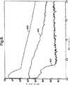
図8は、電気的バイアス処理から生じる様々なレベルのカルシウム沈着を示したSIMSプロットである。図8では、陰極バイアスしたウェハーからのSIMSプロットを450の線で示し、バイアスしていないウェハーからのSIMSプロットを452の線で、また陽極バイアスしたウェハーからのSIMSプロットを454の線で示している。沈着は主として有孔シリコンの表面近くで起こっているが、いずれの場合も11μmの厚さの層全体にわたってカルシウムレベルは背景レベルよりも高かった。450の線は、バイアスしていないウェハーに比べて、陰極バイアスがカルシウム沈着の度合を上昇させ、陽極バイアスはその度合を低下させたことを示している。SIMS測定はまた、有孔シリコン層全体にSBF成分が存在すること、および陰極バイアスの結果として、被覆層内でのある程度の貯留を伴って、フッ素の重要な動きと喪失があったことを示唆した。
電気刺激実験において、in vitroおよびin vivo組織は入力した動力、電流および電圧量の極めて限られた範囲でのみ有利に反応することは広く認められている。これらの範囲は刺激電極の性質を含めた多くの因子に対して感受性である。上述したバイアス実験は、有孔シリコンのカルシウム沈着過程の動態がin vitroで、またそれ故おそらくin vivoでも、陰極バイアスの適用によって加速されうることを示している。また同時に、有孔シリコンとバルクシリコンのような異なるシリコン構造を一緒に生理的電解質に液浸した時、電気侵食過程は、それが生じるいずれの陰極部位でもカルシウム沈着を促進すると考えられる。
無機質沈着のバイアス制御についての潜在的適用は多様である。電極を生きている生物に挿入すると電極の周囲に線維層が形成され、その層の厚さが電極の生物適合性を示すことが知られている。in vivoで微小電極のまわりに安定な無機沈着物が速やかに形成されることは、組織成長の電気刺激あるいは対麻痺患者の筋刺激のために潜在的な恩恵を提供する。無機質沈着の局所的な制御は、その上に無機沈着物が形成されないように限局領域をアレンジすれば、in vivoおよびin vitroでのバイオセンサー装置の分野における適用が得られるであろう。無機質沈着促進の過程は、シリコンベースの集積回路を体内に移植する前に被覆する上で有益であると考えられる。
無機質沈着の電気的制御についての上記の説明は有孔シリコンへの沈着に関するものであるが、SBF溶液中で陽極化していないウェハーに陰極バイアスを適用した時にも無機沈着物が認められた。
さらなる具体例では、特定の種類の多結晶性シリコン(ポリシリコン)はSBF溶液からのリン酸カルシウムの沈着も誘発することができ、従って生物活性であることが認められた。
生物活性な多結晶性シリコンを作製するために、5〜10Ωcmの範囲の抵抗性を持つ直径100mmの〈100〉p型CZシリコンウェハーを、厚さ0.5μmの湿性熱酸化物で、またその後様々な微小構造を持つ厚さ1μmのポリシリコン層で前面および背面被覆する。酸化物層はThermco TMX9000拡散ファーネスにおいて成長させ、ポリシリコン層はThermco TMX9000低圧化学蒸気付着熱壁ファーネスで成長させる。熱酸化物の成長のために、ファーネスの管を1000℃の一定温度に保持し、110分間の蒸気酸化を用いて湿性熱酸化物を成長させる。その後のポリシリコン層の沈着は、ファーネスの管を570〜620℃の範囲に維持しながら、250〜300mtorrの範囲の圧でSiH4を熱分解することを含む。
Kluwer Acad.Publ.1988発行のT.Kaminsによる「Polycrystalline Silicon for Integrated Circuit Applications」の第2章に述べられているように、ポリシリコン層の微小構造が温度、熱、ガス流量および基質の種類のような多くの沈着パラメータに対して感受性であることは広く認められている。570℃、580℃、590℃、600℃、610℃および620℃という異なる沈着温度を用いて、極めて多様な微小構造と形態を持つポリシリコン層が得られた。横断面透過型電子顕微鏡分析は、570℃で沈着させた層がその表面近くでは実質的に非晶質であるのに対し、600℃と620℃で沈着させた層はその深さ全体を通じて多結晶性であることを明らかにした。一定の層に関して、粒子サイズは沈着温度によっていくぶん異なり、深さによって大きく異なる。
次に、0.5×50×20mm3の代表的寸法を持つ分割したウェハー断片を、前述したようにSBF溶液を満たした別々の30cm3のポリエチレンビンに入れ、SBFの温度を37℃±1℃に保持した。横断面SEM画像によって測定すると、様々なポリシリコン層がSBF溶液中で様々なレベルの安定性を持つことが認められた。SBF溶液中に64時間置いた後、620℃で沈着させたポリシリコン層は最初の厚さの約60%まで薄くなったのに対し、570℃で沈着させた層の厚さはSBF溶液中に160時間置いた後も実質的に変化しなかった。
無機沈着物は一部のポリシリコン層の上で核形成し、増殖することが認められた。これらの沈着物を平面SEMを用いて観察した。SBF溶液に2週間液浸した後、600℃と620℃で沈着させたポリシリコン層では無機沈着物が観察されたが、570℃で沈着させた層上には沈着物は観察されなかった。これらの所見は、有孔シリコンに関して、その微小構造に依存して至適生物活性のための反応ウィンドウが存在することを示唆している。無機沈着物の最大密度は600℃で沈着させたポリシリコン層で観察された。重要なレベルの無機沈着物がシリコンウェハーの前面と背面の両方で観察され、両側にポリシリコンの沈着があったことと一致した。
沈着物のEDAX分析は、一部の形態のアパタイトが核形成していたことと一致して、カルシウム、リンおよび酸素の存在を示した。しかし沈着物の形態は先に有孔シリコンに関連して述べた球状体の形態とは異なっており、沈着物はより角張っているよに思われた。この理由は明らかではないが、ポリシリコン上の核形成部位における局所的pHがわずかに異なることを反映していると考えられる。P.LiらはJournal of Applied Biomaterials、4巻、1993、p.221において、シリカゲル上での成長に関してpH7.3で認められるアパタイトの形態がpH7.2で認められるものとは有意に異なることを報告した。
生物活性ポリシリコンの潜在的適用は生物活性有孔シリコンよりも潜在的に広い。単結晶性シリコンでは被覆できない様々な基質をポリシリコンで被覆することが可能である。骨への付着を改善するために外科的インプラントをポリシリコンの層で被覆することができるであろう。ポリシリコンはまたVLSIテクノロジーとも極めて高い適合性があり、複雑な電子回路を生物適合性にする見込みを提示する。様々な装置やパッケージングアレンジメントを作製するために、ポリシリコンを表面微小機械化することができる。
既に、図6を参照してひとつの考えられる生物活性シリコンパッケージングの概念を述べた。生物活性ポリシリコンを用いて、より小さなバイオチップを構築することが可能であろう。図9を参照すると、生物活性ポリシリコンを組み込んだバイオセンサー装置500の図式的概要図が示されている。装置500はバルクシリコンウェハー510を含み、その上にCMOS回路512とセンサーエレメント514が作られている。センサーエレメント514は回路512に電気的に接続されている。回路512は、たとえば酸化シリコンや窒化シリコンのバリア層516によって保護されている。センサーエレメント514へのウィンドウ518を除いて、装置500全体が生物活性ポリシリコンの層520で被覆されている。粒子境界を通過する拡散のためにポリシリコン自体はシリコンベース回路の良好な保護層ではないので、バリア層516が必要である。それ故バリア層516は回路512とポリシリコン層520の間に置かれている。
有孔シリコンを用いた結果から類推して、多結晶性シリコンの生物活性はカルシウム、ナトリウムあるいはリン、あるいはこれらの種の組合せでドープすることによって改善されると考えられる。
生物活性ポリシリコンは生物学的検定装置の適用に適した基質であると考えられる。L.BousseらはIEEE Engineering in Medicine and Biology、1994、p.396−401において、細胞をシリコンチップ上の微小機械化された空洞内に捕獲するin vitro測定を実施するためのバイオセンサーについて述べている。かかる装置はポリシリコンとその上のアパタイト層から成る複合構造を有用に組み込んでおり、細胞はアパタイトの領域上に優先的に位置する。The present invention relates to a biomaterial.
“Biological material” is a non-biological material used in medical devices intended to interact with biological systems. Such materials can be relatively “bioinert”, “biocompatible”, “bioactive” or “resorbable” depending on their in vivo biological response.
Bioactive materials are a class of materials that each induce a specific biological reaction that causes the formation of a bond between the biological tissue and the substance in vivo. Bioactive materials are also referred to as surface reactive biomaterials. A biomaterial can also be defined as a substance suitable for implantation in a living body. L. L. Hench, Science, 208, May 1980, p. Biomaterials were examined in an academic paper published in 826-831. Relatively inert biomaterials can cause interface problems when implanted, and therefore significant research efforts have been made to develop bioactive materials to improve biomaterial-tissue interfaces. I came.
Known bioactive materials include hydroxyapatite (apatite hydroxide) (HA), some glasses and some glass ceramics. Both the bioactive glass and the bioactive glass ceramic form a layer of biologically active hydroxycarbonate apatite (HCA) when implanted. This layer is chemically and structurally equivalent to the mineral phase in the bone and causes interfacial bonding between the bone and the bioactive material. The properties of these bioactive materials are described in Journal of the American Ceramic Society, Vol. 74, No. 7, 1991, p. 1487-1510. L. It is described by Hench. Academic literature on bioactive materials often uses the terms HA and HCA on an interchangeable basis. In this patent specification, HA and HCA materials are collectively referred to as apatite.
Lie et al., Journal of Biomedical Materials Research, 28, 1994, p. 7-15 reported the deposition of apatite on silica gel. They suggest that a certain density of silanol (SiOH) groups is required to cause heteronucleation of hydroxyapatite. An apatite layer is not generated on the surface of the silica glass sample, which is considered to be because the density of surface silanol groups is lower than that of silica gel.
Wang et al., Journal of Materials Science: Materials in Medicine, Vol. 6, 1995, p. As described in 94-104, a thick film of apatite is previously applied to the wafer by placing a silicon single crystal wafer in the immediate vicinity of a glass plate containing apatite and wollastonite soaked in a physiological solution at 36 ° C. Deposited. Physiological solutions, also known as simulated body fluids (SBF), are solutions containing ionic concentrations similar to those found in the human body and are widely used to mimic body reactions in in vitro tests of biological activity. Wang et al. Reported apatite growth on a (111) Si wafer, but also reported that “almost no” apatite could grow on a (100) Si wafer. Silicon wafers themselves are not biologically active. Wang et al., “Si does not play a special role in the growth of apatite coatings, except that Si atoms on the substrate can bind strongly to oxygen atoms in the apatite nucleus and form an interface with low energy. "It has said. The presence of apatite and wollastonite glass is necessary to induce apatite deposition. In fact, Y. Abe et al., Journal of Materials Science: Materials in Medicine,
The ability to use silicon-based integrated circuits in the human body for both diagnostic and therapeutic purposes has long been awaited. Silicon shows low biocompatibility in blood by Kanda et al., Electronics Letters, 17, 16, 1981, p. 558, 559, and currently there is a need for encapsulation with suitable materials to protect the integrated circuit from damage in the biological environment. Medical applications of silicon-based sensors are described in Journal of Physics E: Sci. Instrum. 16, 1983, p. In the papers of Engels et al.
The present invention provides bioactive silicon characterized in that the silicon is at least partially crystalline.
Bioactive silicon offers the advantage of being compatible with silicon-based integrated circuit technology compared to other bioactive materials. It also has the advantage of showing greater biocompatibility compared to non-bioactive silicon. In addition, bioactive silicon can be used to form bonds to living animal bone or vascular tissue. Bioactive silicon can provide a material suitable for use as a packaging material in miniaturized packaging applications.
The bioactive properties of silicon are demonstrated by immersing the material in a simulated body fluid at physiological temperature, which results in the deposition of the material on the bioactive silicon. The inorganic deposit may be apatite. Apatite deposit is 100μm2 It can be continuous over a larger area. The bioactive silicon is at least partially porous silicon. Perforated silicon can have a porosity of more than 4% and less than 70%.
Bulk crystalline silicon can be made porous by partial electrochemical dissolution in a hydrofluoric acid based solution as described in US Pat. No. 5,348,618. This etching process results in a silicon structure that retains the crystallinity and crystallographic orientation of the original bulk material. The porous silicon formed in this way is in the form of crystalline silicon. At low levels of porosity, for example 20% or less, the electronic properties of porous silicon are similar to those of bulk crystalline silicon.
Perforated silicon can be subdivided according to its porosity. Microporous silicon includes pores having a diameter of less than 20 mm; mesoporous silicon includes pores ranging from 20 to 500 mm in diameter; macroporous silicon includes pores having a diameter greater than 500 mm. Bioactive silicon consists of porous silicon, either microporous or mesoporous.
Silicon, in contrast to many metals, ceramics and polymers, has never been evaluated as a promising biomaterial and has not been considered capable of exhibiting a bioactive reaction. In fact, semiconductors have never been reported to be biologically active. At best, silicon is reported to be relatively bioinert but generally poorly biocompatible. Despite advances made in the miniaturization of integrated circuits, silicon VLSI technology has been G. In the chapter “VLSI in Medicine” edited by Einspruch et al., Academic Press, New York, 1989,
The use of silicon structures for biological applications is known. International Patent Application No. PCT / US95 / 025752 with International Application No. WO 95/24472 describes a capsule with an end face formed from a porous amorphous silicon structure, the pores of which are the desired molecules. The product is large enough to let through but block the passage of larger immunological molecules, providing immunological separation of the cells contained within the capsule. There is no evidence of biocompatibility of the silicon structure, and those skilled in the field of biocompatible materials will predict that such devices will stimulate the production of fibrous tissue that occludes pores in vivo. . IEEE Transactions on Biomedical Engineering, 39, No. 6, 1992, p. 635 in D.C. J. et al. As reported by Edell et al., It is known that when a micro-mechanized silicon structure is used as a sensor for a neural element, a layer of fibrous tissue is formed between the silicon surface and the target neural element. Yes. In fact, the thickness and properties of the fibrous tissue layer that is formed are often used as a measure of biocompatibility, the thinner the layer, the less cellular necrosis involved, reflecting higher biocompatibility.
US Pat. No. 5,225,374 uses porous silicon as a substrate for a protein-lipid coating that interacts with a target species to produce an electric current when contacted with the target species in an in vitro solution. Is described. Perforated silicon is selected because it is oxidized to produce a hydrophilic surface, and the pores act as conduits for ion flow, and the structure provides a structural support for the lipid layer. The perforated silicon is separated from the in vitro solution by a protein-lipid coating, so that no problems with the bioactivity or biocompatibility of the perforated silicon occur.
Perforated silicon is an M.I. By Thust et al. Sci. Technol. 7, 1996, p. 26-29 was proposed as a substrate material for in vitro biosensors. In the device structure described therein, porous silicon is subjected to a thermal oxidation process to form a layer of silicon dioxide on the exposed silicon surface of the hole. Since porous silicon is partially thermally oxidized, only silicon dioxide comes into contact with the test solution, so that the bioactivity or biocompatibility of silicon does not matter. Perforated silicon is an effective inert host for enzyme solutions.
E. Richter et al., Journal of Materials Science: Materials in Medicine, Vol. 7, 1996, p. 85-97, and G.P. Fuhr et al., Journal of Micromechanics and Microengineering, Vol. 5, No. 2, 1995, p. 77-85 states that microperforated silicon films can support cellular structures. The silicon film described therein includes a 3 μm thick silicon film drilled by square holes with a width of 5 μm to 20 μm using a lithography process. Mouse embryo fibroblasts were able to grow on the cleaned membrane, but coating the membrane with polylysine improved cell attachment. This paper does not mention the biological activity of the silicon film, nor does it mention the apatite layer formed when it is brought into contact with the cell culture medium. Indeed, given the size of the pores used, the structure is unlikely to show a significant degree of biological activity. Furthermore, it has been recognized by Fuhr et al. That there is a need to discover and develop cytocompatible materials that still have long-term stability.
Journal of Vacuum Science Technology A, Vol. 13, No. 5, 1995, p. 2608-2612. Offenhauser et al. Describe a technique for achieving biocompatibility with a silicon substrate by coating the substrate with an ultra-thin polymer film. Similarly, R.I. S. Potember et al. Proc. 16th International Conference, IEEE Engineering in Medicine and Biology Society, Volume 2, 1994, p. 842-843 describes the use of synthetic peptides attached to silicon surfaces to promote the development of rat neurons.
In another aspect, the present invention provides a bioactive silicon structure characterized in that the silicon is at least partially crystalline.
In yet another aspect, the present invention provides an electronic device for operation within a living human or animal body, wherein the device includes bioactive silicon.
The bioactive silicon of the present invention is placed as a protective coating for electronic circuits and as a means for attaching the device to bone or other tissue.
The electronic device can be a sensor device or a device for intelligent drug delivery delivery or a prosthetic device.
In yet another aspect, the present invention provides a method for rendering silicon bioactive, such method comprising making at least a portion of the silicon porous.
In another aspect, the present invention provides a method for producing bioactive silicon, comprising the step of depositing a layer of polycrystalline silicon.
In yet another aspect, the present invention provides a biocompatible silicon characterized in that the silicon is at least partially crystalline.
In yet another aspect, the present invention provides resorbable silicon.
In another aspect, the present invention provides a method for accelerating or delaying the rate of deposition of inorganic deposits on silicon in a physiological electrolyte, such methods including applying an electrical bias to the silicon.
The silicon can be perforated silicon.
In a further aspect, the present invention provides a bioactive material characterized in that the bioactivity of the material can be controlled by applying an electrical bias to the material.
Conventional bioactive ceramics are electrically insulated and thus have been previously eliminated for use in electrochemical applications. Previously, electrical stimulation of tissue growth was considered, but it was often difficult to distinguish between the direct action of the electric field and the effects associated with biochemical changes near the implanted “bioinert” electrode.
In yet another aspect, the present invention provides a composite structure consisting of a bioactive silicon region and an inorganic deposit thereon, characterized in that the silicon region comprises silicon that is at least partially crystalline.
A possible application of the present invention is as a substrate for performing biological assays. It would be desirable to be able to perform certain tests on drug compounds without resorting to animal in vivo tests. Therefore, much research effort has been devoted to developing in vitro tests that support a cell line on a substrate and monitor the action of drug compounds on the cell line. The composite structure of silicon and apatite provides a suitable substrate for such testing.
In a further aspect, the present invention provides a method for manufacturing a biosensor, comprising the step of forming a composite structure consisting of bioactive silicon and inorganic deposits thereon.
The present invention further provides a biosensor comprising a silicon substrate for testing the pharmacological activity of a compound, characterized in that at least a part of the silicon substrate consists of bioactive silicon.
In order that the present invention may be more fully understood, specific examples thereof are set forth below, by way of example only, with reference to the accompanying figures in which:
FIG. 1 is a schematic cross-sectional view of a bioactive silicon wafer;
2 is an image of a scanning electron microscope (SEM) photograph of an apatite deposit on a bulk silicon region adjacent to the perforated region of the wafer of FIG. 1;
FIG. 3 is an image of a SEM photograph of a cross section of the silicon region of FIG. 2;
Figure 4 is an image of an SEM photograph showing apatite spheres deposited on a porous 31% porous silicon region;
FIG. 5a is an image of an SEM photograph of a non-anodized region of a silicon wafer anodized to yield 48% porosity after immersion in simulated body fluid;
Figure 5b is an image of a SEM photograph of the anodized region of the wafer of Figure 5a;
FIG. 6 is a schematic overview of a biosensor that includes bioactive silicon;
FIG. 7 is a schematic overview of an electrochemical cell for electrical control of biological activity;
FIG. 8 is a diagram of the profile of calcium concentration in a perforated silicon wafer after processing in the cell of FIG. 7;
FIG. 9 is a schematic overview of a biosensor device that includes the bioactive polycrystalline silicon of the present invention.
Referring to FIG. 1, a cross section of a bioactive silicon wafer, indicated generally at 10, is shown. The
In order to measure the biological activity of the anodized wafer, the divided wafer pieces were placed in simulated body fluid (SBF) for a period of 2 hours to 6 weeks. SBF solutions were prepared by dissolving reagent grade salts in deionized water. The solution contained an ionic concentration similar to that found in human plasma. Table 1 shows the ion concentrations of the SBF solution and human plasma. The SBF solution was organically buffered with trihydroxymethylaminomethane and hydrochloric acid at a pH of 7.30 ± 0.05 equal to physiological pH. The perforated wafer was stored in ambient air for at least several months prior to immersion in the SBF solution, so the perforated silicon wafer was hydrated. The perforated silicon thus included a silicon framework coated with a thin native oxide similar to that formed on bulk silicon as a result of storage in air.
After a known period, the pieces were removed from the SBF solution, washed with deionized water, dried in ambient air, and characterized. SBF-treated fragments were examined using x-ray microanalysis (EDX) with a scanning electron microscope (SEM) and a JEOL 6400F microscope. Secondary ion mass spectrometry was performed using a Cameca 4F instrument and infrared spectroscopy was performed using a Biorad FTS-40 spectrometer.
After immersion periods of 2, 4 and 17 hours of SBF solution, negligible apatite deposits occurred in both the
Referring to FIG. 2, a reproduction of the SEM micrograph, indicated generally at 50, is shown. The
Referring to FIG. 3, there is shown a reproduction of an SEM micrograph of a cross section of
SEM analysis of the
The formation of apatite deposits was also observed for wafers where the porosity of the porous silicon was other than 18%. A microporous wafer with a perforated 31% perforated silicon region was taken from a strongly boron-doped p-type CZ silicon wafer at 0.03 Ωcm at 100 mA / cm for 1 minute in 50 wt% HF.2 And anodizing at an anodizing current density of The resulting perforated silicon area is 9.4 μm thick and 250 m2 It had a surface area per unit mass of / g. The perforated silicon wafer was immersed in the SBF solution after a considerable period of time.
FIG. 4 shows an image of an SEM micrograph of the surface of a porous 31% porous silicon layer after immersion of the wafer piece in 30 cm 3 SBF solution, usually indicated at 150, for 7 days. The
A microporous wafer with a porous silicon region of 48% porous, a light boron-doped p-type silicon wafer with a resistance of 30 Ωcm, and 20 mA / cm in 50 wt% HF.2 And anodizing for 5 minutes. The resulting porous silicon area is 6.65 μm thick and about 800 m.2 It had a surface area per unit mass of / g. The perforated silicon wafer pieces were 150 cm filled with SBF solution after a considerable period of time.Three In a polyethylene bottle.
FIG. 5a shows an image of a SEM micrograph of
Some forms of perforated silicon are known to be glitter. The presence of red or orange glitter from the perforated silicon generally indicates the presence of quantum wires or quantum dots of silicon material. A 48% porous wafer that has passed a considerable period of time before being immersed in the SBF solution is bright and has a high concentration of porous silicon regions despite being hydrated by contact with ambient air. It is suggested to hold quantum wires or dots. The emission characteristics were preserved during and after immersion in the SBF solution. This indicates that the apatite is deposited on the porous silicon so as to preserve the luminescent properties. Preservation of luminescent properties after apatite layer growth is considered to be a useful property for the development of electro-optic biosensors.
70% porous, surface area 640m per unit mass2 A fully mesoporous, light-emitting, perforated silicon wafer with a perforated area of 1 g / g, was placed in the SBF solution. After approximately 1 day, the perforated area was dissolved and completely removed in the SBF solution and the wafer was no longer luminescent. No apatite deposits were observed in either the porous silicon region or the non-porous region. Mesoporous silicon is more effectively hydrated by the SBF solution, and therefore mesoporous silicon is considered to have a higher dissolution rate than microporous silicon. Therefore, mesoporous silicon exhibits resorbable biomaterial properties. It is believed possible to build a bioactive silicon structure with a limited area of mesoporous silicon that acts as a source of soluble silicon. This will result in a locally saturated silicon solution and thus can promote apatite deposition.
A large-pore silicon wafer with a porous region of 4% porosity and a thickness of 38 μm is a bulk non-anodized silicon wafer that does not show apatite deposit growth when immersed in SBF solution for 4 weeks. Acted the same way. Further, no apatite growth was observed in a porous silicon region having a porosity of 80% and a thickness of 50 μm, but this region retains its light emission characteristics even after being immersed in an SBF solution for 2 weeks.
As a further control, a split non-perforated silicon wafer fragment of the same dimensions as the perforated silicon wafer fragment is 30 cm.Three In an SBF solution. After immersion for 5 weeks in SBF solution, 5000 / cm2 The following very low density micron sized deposits were observed: These deposits were probably located at surface defect sites on the silicon wafer. Therefore, bulk non-porous silicon is not bioactive. This is because the growth rate of the apatite deposit is too slow to form a bond with the living tissue.
Thus, these experiments suggest that by appropriately controlling the pore size and porosity, the silicon structure can cover substantially the entire bioactivity spectrum. Bulk, purely macroporous silicon is relatively bioinert; highly porous mesoporous silicon is resorbable and moderately porous microporous silicon is bioactive.
It is known that changes in the chemical composition of biomaterials can also affect whether they are bioinert, resorbable or bioactive. The above experiments were performed on a perforated silicon wafer that was not intentionally doped with specific elements other than impurity doping to control the semiconductor properties of silicon. SiO2 , Na2 O, CaO and P2 OFive It is believed that calcium elution from bioactive glasses containing contains significantly helps apatite growth by promoting local supersaturation. 20 mA / cm in 40% aqueous HF2 For one minute to allow calcium to penetrate a freshly corroded layer of microporous silicon with a porosity of 55% and a thickness of 1.2 μm formed in a lightly doped p-type (30 Ωcm) CZ silicon wafer. It was. Calcium penetration is 125cmThree 5 g CaCl. 2H2 Performed through mild oxidation by storage in a solution containing O. Permeation of porous silicon with calcium, sodium or phosphorus or a combination of these species is believed to promote the formation of apatite on silicon.
After immersion in the SBF solution, the presence of a silicon oxide layer under the apatite deposit in the non-porous region adjacent to the porous silicon region of the anodized wafer indicates that silicon is dissolved from the porous silicon region. Suggests that it is an important factor for the biological activity of porous silicon. It is believed that the dissolution of silicon forms a locally supersaturated solution that causes the deposition of a porous silicon oxide layer. Apatite is then deposited on the porous silicon oxide. This is because various non-porous crystalline, polycrystalline or amorphous silicon based structures that are more soluble in SBF solutions than normal bulk crystalline silicon and contain impregnated calcium. Suggests that it is active. To significantly help apatite growth, the crystallinity of silicon does not necessarily have to be preserved, but the level of calcium permeation is much higher than previously reported calcium-doped silicon. is necessary.
Calcium is generally regarded as a less attractive dopant for silicon, and as a result, there has been little testing on calcium doped silicon. Journal of the Electrochemical Society, 129, 1982, p. In 2809-2812, Sigmad has a maximum equilibrium solubility of 6.0 × 10 6 for calcium in single crystalline silicon.18 / CmThree It is reported that. At this concentration, calcium is believed not to have a significant effect on apatite growth. 10twenty one / CmThree Supersaturated levels of calcium in concentrations exceeding (2%) are required. Such very high concentrations can be achieved by the following steps:
(A) solution doping of porous silicon as described above;
(B) Ion permeation of porous silicon or bulk silicon with calcium ions; or
(C) Epitaxy deposition of calcium or calcium compounds followed by heat treatment.
Referring to FIG. 6, a schematic overview of a generalized sensor for medical applications incorporating bioactive silicon, indicated generally at 300, is shown.
In addition to sensors, bioactive silicon has found application in electronic prosthetic devices, such as the artificial eye. Other electronic devices that can include bioactive silicon include intelligent drug delivery systems.
In addition to sensors for incorporation into human and other animal bodies, bioactive porous silicon can also be used in the manufacture of biosensors for in vitro applications. A composite structure consisting of porous silicon and an apatite layer thereon is believed to have improved cytocompatibility compared to prior art biosensor devices. Biosensors are potentially very important in the field of in vitro pharmaceutical testing. For automated pharmaceutical testing, the biological assay device can include a silicon wafer with a substrate array of perforated silicon regions. The cell can be placed selectively in the perforated silicon area, which will facilitate automatic cell analysis after contact with the drug. The luminescent properties of perforated silicon can be used to enable optical cell analysis techniques. Those skilled in the biosensor art will use that experience to identify which cell cultures are appropriate and how cell behavior can be monitored.
Although the results of in vitro experiments have been described, no in vivo experiments have been described. However, in vitro experiments are planned to mimic the environment within the human body. From the results of in vitro experiments, it can be concluded that silicon wafers that produced significant apatite deposits in the SBF solution will also exhibit bioactive behavior in vivo.
The formation of apatite coatings on silicon or perforated silicon surfaces in vitro suggests that the bioactive silicon is, to some extent, a biocompatible form of silicon. The term “biocompatible” means that the material is not necessarily biologically acceptable for all applications, but can be biologically acceptable for a particular application. One skilled in the biocompatibility field may consider “histocompatibility” as a more appropriate term to describe this definition of biocompatibility. The apatite layer is considered to act as a protective barrier that suppresses the physiological action of silicon.
As described above, mesoporous silicon exhibits resorbable biomaterial properties. From the paper by Hench in the Journal of the American Ceramic Society cited above, resorbable biomaterials are materials that are designed to gradually degrade over time and replace natural host tissue. is there. The properties of mesoporous silicon in simulated body fluids suggest that a suitable mesoporous mesoporous silicon is a resorbable biomaterial. As discussed above, the
Dissolution of porous silicon in SBF solution suggests resorbable biomaterial properties, but the reaction of porous silicon regions in vivo is thought to be influenced by factors that cannot be reproduced in SBF solution. . If living cells grow on the surface of porous silicon, these cells are thought to interact with the porous silicon. Therefore, experiments conducted with SBF solutions do not clearly indicate whether a particular form of perforated silicon is compatible with the application of resorbable materials. In vivo experiments will be conducted to determine if a particular desired physiological response is achieved.
Further experiments were performed that show that the application of a bias current in SBF solution can promote or retard the formation of apatite layers on porous silicon.
Referring to FIG. 7, a schematic overview of an
The
After 3 hours of SBF contact, the surface of the perforated silicon wafer was examined with an acceleration potential of 6 kV in a JEOL 6400F scanning electron microscope (SEM). Wafers that were anodic biased and holed showed no evidence of surface deposits on the perforated silicon, along with a control wafer that was holed without bias. However, the cathode biased wafer was completely covered with spheres that merged to form a continuous layer. Planar EDX analysis shows that this coating layer is inorganic, mainly containing calcium and phosphorus, and contains other SBF components such as carbon, magnesium, sodium and chlorine that are close to the detection limit of EDX (ie, <1 atomic%). Indicated. Planar EDX analysis of unbiased and anodic biased wafers showed only the presence of silicon and oxygen.
Cross-sectional SEM and EDX analysis showed that the calcium and phosphorus rich minerals produced under the cathodic bias were confined to the top of the porous silicon layer and were relatively thin and about 0.2 μm thick. . Within the perforated silicon, the calcium and phosphorus levels for all samples are below the EDX detection limit. The anodic loaded porous silicon layer showed significant oxygen accumulation within the upper 0.5 μm of the layer.
Secondary ion mass spectrometry (SIMS) was used to compare the extent and depth of calcification of layers after three different treatments, as well as the depth distribution of other specific elements. Freshly etched microporous silicon, for example, showed very low levels of calcium and sodium (present in SBF), but contained appreciable levels of fluorine (not present in SBF).
FIG. 8 is a SIMS plot showing various levels of calcification resulting from electrical biasing. In FIG. 8, the SIMS plot from the cathode biased wafer is shown as 450 lines, the SIMS plot from the unbiased wafer is shown as 452 lines, and the SIMS plot from the anode biased wafer is shown as 454 lines. Yes. Although deposition occurred primarily near the surface of the perforated silicon, in all cases the calcium level was higher than the background level throughout the 11 μm thick layer. The 450 line shows that the cathode bias increased the degree of calcium deposition and the anode bias decreased the degree compared to an unbiased wafer. SIMS measurements also suggest that there was an SBF component throughout the porous silicon layer and that there was significant movement and loss of fluorine with some retention in the coating layer as a result of the cathode bias. did.
In electrical stimulation experiments, it is widely accepted that in vitro and in vivo tissues react favorably only in a very limited range of input power, current and voltage. These ranges are sensitive to many factors including the nature of the stimulating electrode. The bias experiments described above show that the kinetics of the porous silicon calcification process can be accelerated by the application of a cathode bias in vitro, and possibly even in vivo. At the same time, when different silicon structures such as porous silicon and bulk silicon are immersed together in a physiological electrolyte, the electroerosion process is thought to promote calcium deposition at any cathode site where it occurs.
The potential applications for bias control of mineral deposition are diverse. It is known that when an electrode is inserted into a living organism, a fibrous layer is formed around the electrode, and the thickness of the layer indicates the biocompatibility of the electrode. The rapid formation of stable inorganic deposits around the microelectrodes in vivo provides potential benefits for electrical stimulation of tissue growth or muscle stimulation of paraplegic patients. Local control of mineral deposition will have application in the field of biosensor devices in vivo and in vitro if the localized area is arranged so that no inorganic deposits are formed thereon. The process of promoting mineral deposition is considered beneficial for coating silicon-based integrated circuits prior to implantation in the body.
While the above description of electrical control of inorganic deposition relates to deposition on porous silicon, inorganic deposits were also observed when a cathode bias was applied to a wafer that was not anodized in SBF solution.
In a further embodiment, it has been found that certain types of polycrystalline silicon (polysilicon) can also induce the deposition of calcium phosphate from SBF solutions and are therefore bioactive.
To make bioactive polycrystalline silicon, a 100 mm diameter <100> p-type CZ silicon wafer with a resistance in the range of 5 to 10 Ωcm was made with a 0.5 μm thick wet thermal oxide and then The front and back surfaces are covered with a 1 μm thick polysilicon layer having various microstructures. The oxide layer is grown in a Thermco TMX9000 diffusion furnace and the polysilicon layer is grown in a Thermco TMX9000 low pressure chemical vapor deposition hot wall furnace. For thermal oxide growth, the furnace tube is held at a constant temperature of 1000 ° C. and the wet thermal oxide is grown using steam oxidation for 110 minutes. Subsequent deposition of the polysilicon layer is accomplished with SiH at a pressure in the range of 250-300 mtorr while maintaining the furnace tube in the range of 570-620 ° C.Four Including thermal decomposition.
Kluwer Acad. Publ. T. 1988 issued. As described in Chapter 2 of “Polycrystalline Silicon for Integrated Circuit Applications” by Kamins, the microstructure of the polysilicon layer is sensitive to many deposition parameters such as temperature, heat, gas flow rate, and substrate type. Is widely accepted. Using different deposition temperatures of 570 ° C., 580 ° C., 590 ° C., 600 ° C., 610 ° C. and 620 ° C., polysilicon layers with very diverse microstructures and morphologies were obtained. Cross-sectional transmission electron microscopy analysis shows that the layer deposited at 570 ° C. is substantially amorphous near its surface, while the layers deposited at 600 ° C. and 620 ° C. are many throughout its depth. It was revealed that it was crystalline. For a given layer, the particle size varies somewhat with deposition temperature and varies greatly with depth.
Next, 0.5 x 50 x 20 mmThree The divided wafer pieces having typical dimensions of 30 cm are separated into separate 30 cm filled with SBF solution as described above.Three The SBF temperature was maintained at 37 ° C. ± 1 ° C. As measured by cross-sectional SEM images, various polysilicon layers were found to have various levels of stability in SBF solutions. After 64 hours in the SBF solution, the polysilicon layer deposited at 620 ° C. was thinned to about 60% of the original thickness, whereas the thickness of the layer deposited at 570 ° C. was reduced in the SBF solution. No change was observed after 160 hours.
Inorganic deposits were found to nucleate and grow on some polysilicon layers. These deposits were observed using a planar SEM. After immersion in the SBF solution for 2 weeks, inorganic deposits were observed in the polysilicon layer deposited at 600 ° C. and 620 ° C., but no deposit was observed on the layer deposited at 570 ° C. These findings suggest that there is a reaction window for optimal biological activity for porous silicon, depending on its microstructure. The maximum density of inorganic deposits was observed with polysilicon layers deposited at 600 ° C. Significant levels of inorganic deposits were observed on both the front and back of the silicon wafer, consistent with polysilicon deposition on both sides.
EDAX analysis of the deposits showed the presence of calcium, phosphorus and oxygen, consistent with some form of apatite nucleating. However, the deposit morphology was different from that of the spheroids described above in connection with the porous silicon, and the deposit appeared to be more angular. The reason for this is not clear, but is thought to reflect a slightly different local pH at the nucleation site on the polysilicon. P. Li et al., Journal of Applied Biomaterials, 4, 1993, p. 221 reported that the apatite morphology observed at pH 7.3 for growth on silica gel was significantly different from that observed at pH 7.2.
The potential application of bioactive polysilicon is potentially broader than bioactive porous silicon. Various substrates that cannot be coated with monocrystalline silicon can be coated with polysilicon. Surgical implants could be covered with a layer of polysilicon to improve bone attachment. Polysilicon is also very compatible with VLSI technology, presenting the prospect of making complex electronic circuits biocompatible. Polysilicon can be surface micromachined to make various devices and packaging arrangements.
Already, one possible bioactive silicon packaging concept has been described with reference to FIG. It would be possible to build smaller biochips using bioactive polysilicon. Referring to FIG. 9, a schematic overview of a
By analogy with the results using porous silicon, it is believed that the biological activity of polycrystalline silicon is improved by doping with calcium, sodium or phosphorus, or combinations of these species.
Bioactive polysilicon is considered to be a suitable substrate for bioassay device applications. L. Bousse et al., IEEE Engineering in Medicine and Biology, 1994, p. 396-401 describes a biosensor for performing in vitro measurements that trap cells in a micromechanical cavity on a silicon chip. Such devices usefully incorporate a composite structure consisting of polysilicon and an apatite layer thereon, with cells preferentially located on the apatite region.
Claims (15)
Translated fromJapanese直径20Å未満の孔サイズを有する微小孔性シリコンであって、シリコンの有孔性が4%より多く70%未満である前記生物活性シリコンであり、
36〜38℃に保持した擬似体液溶液に液侵した時、シリコンがその上にアパタイトの沈着を誘発すること、及び当該アパタイトが少なくとも100μm2の面積にわたって連続的であることを特徴とする前記生物活性シリコン。Bioactive silicon that interacts with biological tissue to form a bond between silicon and biological tissue,
A microporous silicon having a pore size of less than 20 mm in diameter, wherein the silicon has a porosity of more than 4% and less than 70%;
Silicone induces the deposition of apatite thereon when immersed in a simulated body fluid solution maintained at 36-38 ° C.,and the organism is continuous over an area ofat least 100 μm2Active silicon .
直径が20Åから500Åまでの範囲である孔サイズを有する中孔性シリコンであって、シリコンの有孔性が4%より多く70%未満である前記生物活性シリコンであり、
36〜38℃に保持した擬似体液溶液に液侵した時、シリコンがその上にアパタイトの沈着を誘発すること、及び当該アパタイトが少なくとも100μm2の面積にわたって連続的であることを特徴とする前記生物活性シリコン。Bioactive silicon that interacts with biological tissue to form a bond between silicon and biological tissue,
A mesoporous silicon having a pore size ranging from 20 to 500 mm in diameter, wherein the silicon has a porosity of more than 4% and less than 70%;
Silicone induces the deposition of apatite thereon when immersed in a simulated body fluid solution maintained at 36-38 ° C.,and the organism is continuous over an area ofat least 100 μm2Active silicon .
Applications Claiming Priority (7)
| Application Number | Priority Date | Filing Date | Title |
|---|---|---|---|
| GB9515956AGB2303847A (en) | 1995-08-03 | 1995-08-03 | Bioactive silicon |
| GB9524242.6 | 1995-11-28 | ||
| GBGB9524242.6AGB9524242D0 (en) | 1995-08-03 | 1995-11-28 | Biomaterial |
| GB9515956.2 | 1996-05-31 | ||
| GBGB9611437.6AGB9611437D0 (en) | 1995-08-03 | 1996-05-31 | Biomaterial |
| GB9611437.6 | 1996-05-31 | ||
| PCT/GB1996/001863WO1997006101A1 (en) | 1995-08-03 | 1996-08-01 | Biomaterial |
Related Child Applications (1)
| Application Number | Title | Priority Date | Filing Date |
|---|---|---|---|
| JP2007258623ADivisionJP2008086775A (en) | 1995-08-03 | 2007-10-02 | Biomaterial |
Publications (2)
| Publication Number | Publication Date |
|---|---|
| JPH11510469A JPH11510469A (en) | 1999-09-14 |
| JP4251664B2true JP4251664B2 (en) | 2009-04-08 |
Family
ID=27267841
Family Applications (2)
| Application Number | Title | Priority Date | Filing Date |
|---|---|---|---|
| JP50821497AExpired - LifetimeJP4251664B2 (en) | 1995-08-03 | 1996-08-01 | Biomaterial |
| JP2007258623AWithdrawnJP2008086775A (en) | 1995-08-03 | 2007-10-02 | Biomaterial |
Family Applications After (1)
| Application Number | Title | Priority Date | Filing Date |
|---|---|---|---|
| JP2007258623AWithdrawnJP2008086775A (en) | 1995-08-03 | 2007-10-02 | Biomaterial |
Country Status (7)
| Country | Link |
|---|---|
| US (3) | US6322895B1 (en) |
| EP (1) | EP0842113A1 (en) |
| JP (2) | JP4251664B2 (en) |
| AU (1) | AU6626496A (en) |
| CA (1) | CA2228426C (en) |
| GB (2) | GB9611437D0 (en) |
| WO (1) | WO1997006101A1 (en) |
Families Citing this family (201)
| Publication number | Priority date | Publication date | Assignee | Title |
|---|---|---|---|---|
| US10028851B2 (en) | 1997-04-15 | 2018-07-24 | Advanced Cardiovascular Systems, Inc. | Coatings for controlling erosion of a substrate of an implantable medical device |
| US6240616B1 (en) | 1997-04-15 | 2001-06-05 | Advanced Cardiovascular Systems, Inc. | Method of manufacturing a medicated porous metal prosthesis |
| US8172897B2 (en) | 1997-04-15 | 2012-05-08 | Advanced Cardiovascular Systems, Inc. | Polymer and metal composite implantable medical devices |
| US6776792B1 (en) | 1997-04-24 | 2004-08-17 | Advanced Cardiovascular Systems Inc. | Coated endovascular stent |
| US20030008396A1 (en)* | 1999-03-17 | 2003-01-09 | Ku David N. | Poly(vinyl alcohol) hydrogel |
| US6117643A (en)* | 1997-11-25 | 2000-09-12 | Ut Battelle, Llc | Bioluminescent bioreporter integrated circuit |
| GB9808052D0 (en) | 1998-04-17 | 1998-06-17 | Secr Defence | Implants for administering substances and methods of producing implants |
| GB9815819D0 (en) | 1998-07-22 | 1998-09-16 | Secr Defence | Transferring materials into cells and a microneedle array |
| AU2003200223B2 (en)* | 1998-07-22 | 2005-05-05 | Psimedica Limited | Transferring materials into cells using resorbable silicon |
| CN1365292A (en)* | 1999-05-01 | 2002-08-21 | 秦内蒂克有限公司 | Derivatized porous silicon |
| GB9924334D0 (en)* | 1999-10-15 | 1999-12-15 | Secr Defence | Pharmaceutical products and methods of fabrication therefor |
| DE19955618A1 (en)* | 1999-11-19 | 2001-05-23 | Heidenhain Gmbh Dr Johannes | Measurement body and opto-electronic position measurement device, in which scattered light is minimized, for scanning alternating regions of luminescent and non-luminescent material along a measurement direction |
| US6890640B2 (en)* | 1999-12-03 | 2005-05-10 | Caterpillar Inc | Patterned hydrophilic-oleophilic metal oxide coating and method of forming |
| GB9929521D0 (en) | 1999-12-15 | 2000-02-09 | Secr Defence | Bonded products and methods of fabrication therefor |
| GB0008494D0 (en) | 2000-04-07 | 2000-05-24 | Secr Defence | Microprojectile delivery system |
| GB2363115A (en)* | 2000-06-10 | 2001-12-12 | Secr Defence | Porous or polycrystalline silicon orthopaedic implants |
| AU2005200352B2 (en)* | 2000-06-10 | 2008-05-15 | Psimedica Limited | A porous and/or polycrystalline silicon orthopaedic implant |
| GB2365769A (en)* | 2000-08-18 | 2002-02-27 | Secr Defence | Skin preparations containing silicon |
| US6783793B1 (en) | 2000-10-26 | 2004-08-31 | Advanced Cardiovascular Systems, Inc. | Selective coating of medical devices |
| US6881198B2 (en)* | 2001-01-09 | 2005-04-19 | J. David Brown | Glaucoma treatment device and method |
| WO2002068957A1 (en) | 2001-02-21 | 2002-09-06 | University Of Rochester | Microcavity biosensor, methods of making, and uses thereof |
| GB0104383D0 (en)* | 2001-02-22 | 2001-04-11 | Psimedica Ltd | Cancer Treatment |
| US7695521B2 (en) | 2001-05-01 | 2010-04-13 | Amedica Corporation | Hip prosthesis with monoblock ceramic acetabular cup |
| US7776085B2 (en) | 2001-05-01 | 2010-08-17 | Amedica Corporation | Knee prosthesis with ceramic tibial component |
| EP1408874B1 (en) | 2001-06-14 | 2012-08-08 | Amedica Corporation | Metal-ceramic composite articulation |
| US6565659B1 (en) | 2001-06-28 | 2003-05-20 | Advanced Cardiovascular Systems, Inc. | Stent mounting assembly and a method of using the same to coat a stent |
| GB0118689D0 (en)* | 2001-08-01 | 2001-09-19 | Psimedica Ltd | Pharmaceutical formulation |
| GB0120202D0 (en)* | 2001-08-18 | 2001-10-10 | Psimedica | Body fluid collection and analysis |
| US7989018B2 (en) | 2001-09-17 | 2011-08-02 | Advanced Cardiovascular Systems, Inc. | Fluid treatment of a polymeric coating on an implantable medical device |
| US7285304B1 (en) | 2003-06-25 | 2007-10-23 | Advanced Cardiovascular Systems, Inc. | Fluid treatment of a polymeric coating on an implantable medical device |
| US6863683B2 (en) | 2001-09-19 | 2005-03-08 | Abbott Laboratoris Vascular Entities Limited | Cold-molding process for loading a stent onto a stent delivery system |
| DE10152002A1 (en)* | 2001-10-22 | 2003-05-08 | Infineon Technologies Ag | Semiconductor device with a multilayer structure and method for its production |
| GB0130608D0 (en) | 2001-12-21 | 2002-02-06 | Psimedica Ltd | Medical fibres and fabrics |
| US8271202B1 (en)* | 2002-02-11 | 2012-09-18 | Fernandez Dennis S | Modified host bio-data management |
| US20060083791A1 (en) | 2002-05-24 | 2006-04-20 | Moerck Rudi E | Rare earth metal compounds methods of making, and methods of using the same |
| US20040161474A1 (en)* | 2002-05-24 | 2004-08-19 | Moerck Rudi E. | Rare earth metal compounds methods of making, and methods of using the same |
| US6989897B2 (en)* | 2002-06-12 | 2006-01-24 | Intel Corporation | Metal coated nanocrystalline silicon as an active surface enhanced Raman spectroscopy (SERS) substrate |
| US7361313B2 (en)* | 2003-02-18 | 2008-04-22 | Intel Corporation | Methods for uniform metal impregnation into a nanoporous material |
| US6970239B2 (en)* | 2002-06-12 | 2005-11-29 | Intel Corporation | Metal coated nanocrystalline silicon as an active surface enhanced Raman spectroscopy (SERS) substrate |
| US7758881B2 (en) | 2004-06-30 | 2010-07-20 | Advanced Cardiovascular Systems, Inc. | Anti-proliferative and anti-inflammatory agent combination for treatment of vascular disorders with an implantable medical device |
| US8435550B2 (en) | 2002-12-16 | 2013-05-07 | Abbot Cardiovascular Systems Inc. | Anti-proliferative and anti-inflammatory agent combination for treatment of vascular disorders with an implantable medical device |
| AU2003297195A1 (en) | 2002-12-17 | 2004-07-22 | Amedica Corporation | Total disc implant |
| JP4890764B2 (en)* | 2002-12-18 | 2012-03-07 | ザ リージェンツ オブ ザ ユニバーシティ オブ カリフォルニア | Biocompatible hydrogel bone-like complex |
| GB2399014A (en)* | 2003-01-31 | 2004-09-08 | Psimedica Ltd | Device comprising resorbable silicon for boron neutron capture therapy |
| US20060122596A1 (en)* | 2003-04-17 | 2006-06-08 | Nanosys, Inc. | Structures, systems and methods for joining articles and materials and uses therefor |
| US7074294B2 (en)* | 2003-04-17 | 2006-07-11 | Nanosys, Inc. | Structures, systems and methods for joining articles and materials and uses therefor |
| US20050221072A1 (en)* | 2003-04-17 | 2005-10-06 | Nanosys, Inc. | Medical device applications of nanostructured surfaces |
| US7579077B2 (en)* | 2003-05-05 | 2009-08-25 | Nanosys, Inc. | Nanofiber surfaces for use in enhanced surface area applications |
| US20050038498A1 (en)* | 2003-04-17 | 2005-02-17 | Nanosys, Inc. | Medical device applications of nanostructured surfaces |
| US7056409B2 (en)* | 2003-04-17 | 2006-06-06 | Nanosys, Inc. | Structures, systems and methods for joining articles and materials and uses therefor |
| US7972616B2 (en)* | 2003-04-17 | 2011-07-05 | Nanosys, Inc. | Medical device applications of nanostructured surfaces |
| WO2005005679A2 (en)* | 2003-04-28 | 2005-01-20 | Nanosys, Inc. | Super-hydrophobic surfaces, methods of their construction and uses therefor |
| US7803574B2 (en)* | 2003-05-05 | 2010-09-28 | Nanosys, Inc. | Medical device applications of nanostructured surfaces |
| TWI427709B (en)* | 2003-05-05 | 2014-02-21 | Nanosys Inc | Nanofiber surfaces for use in enhanced surface area applications |
| ITTO20030409A1 (en)* | 2003-06-03 | 2004-12-04 | Fiat Ricerche | OPTICAL BIOSENSOR. |
| JP4438049B2 (en)* | 2003-08-11 | 2010-03-24 | キヤノン株式会社 | Field effect transistor, sensor using the same, and manufacturing method thereof |
| US7198675B2 (en) | 2003-09-30 | 2007-04-03 | Advanced Cardiovascular Systems | Stent mandrel fixture and method for selectively coating surfaces of a stent |
| GB0324483D0 (en)* | 2003-10-21 | 2003-11-19 | Psi Medica Ltd | Composite material |
| SI1677828T1 (en)* | 2003-10-21 | 2013-04-30 | Psimedica Limited | Composite material comprising a porous semiconductor impregnated with an organic substance |
| DE10353995A1 (en)* | 2003-11-19 | 2005-06-09 | Degussa Ag | Nanoscale, crystalline silicon powder |
| US7563324B1 (en) | 2003-12-29 | 2009-07-21 | Advanced Cardiovascular Systems Inc. | System and method for coating an implantable medical device |
| GB2409924A (en) | 2004-01-06 | 2005-07-13 | Psimedica Ltd | Method of making a silicon-phosphorus composite |
| US8025960B2 (en) | 2004-02-02 | 2011-09-27 | Nanosys, Inc. | Porous substrates, articles, systems and compositions comprising nanofibers and methods of their use and production |
| US20110039690A1 (en) | 2004-02-02 | 2011-02-17 | Nanosys, Inc. | Porous substrates, articles, systems and compositions comprising nanofibers and methods of their use and production |
| WO2005077304A1 (en) | 2004-02-06 | 2005-08-25 | Georgia Tech Research Corporation | Load bearing biocompatible device |
| EP1786485A4 (en) | 2004-02-06 | 2012-05-30 | Georgia Tech Res Inst | Surface directed cellular attachment |
| US7553377B1 (en) | 2004-04-27 | 2009-06-30 | Advanced Cardiovascular Systems, Inc. | Apparatus and method for electrostatic coating of an abluminal stent surface |
| GB2414231A (en)* | 2004-05-21 | 2005-11-23 | Psimedica Ltd | Porous silicon |
| CN103646848B (en) | 2004-06-04 | 2018-06-05 | 伊利诺伊大学评议会 | The method of assembling printable semiconductor elements and manufacture electronic device |
| US20050278025A1 (en)* | 2004-06-10 | 2005-12-15 | Salumedica Llc | Meniscus prosthesis |
| US8568469B1 (en) | 2004-06-28 | 2013-10-29 | Advanced Cardiovascular Systems, Inc. | Stent locking element and a method of securing a stent on a delivery system |
| US8241554B1 (en) | 2004-06-29 | 2012-08-14 | Advanced Cardiovascular Systems, Inc. | Method of forming a stent pattern on a tube |
| US8747878B2 (en) | 2006-04-28 | 2014-06-10 | Advanced Cardiovascular Systems, Inc. | Method of fabricating an implantable medical device by controlling crystalline structure |
| US7971333B2 (en) | 2006-05-30 | 2011-07-05 | Advanced Cardiovascular Systems, Inc. | Manufacturing process for polymetric stents |
| US8747879B2 (en) | 2006-04-28 | 2014-06-10 | Advanced Cardiovascular Systems, Inc. | Method of fabricating an implantable medical device to reduce chance of late inflammatory response |
| US8778256B1 (en) | 2004-09-30 | 2014-07-15 | Advanced Cardiovascular Systems, Inc. | Deformation of a polymer tube in the fabrication of a medical article |
| US7731890B2 (en) | 2006-06-15 | 2010-06-08 | Advanced Cardiovascular Systems, Inc. | Methods of fabricating stents with enhanced fracture toughness |
| US9283099B2 (en) | 2004-08-25 | 2016-03-15 | Advanced Cardiovascular Systems, Inc. | Stent-catheter assembly with a releasable connection for stent retention |
| US7229471B2 (en) | 2004-09-10 | 2007-06-12 | Advanced Cardiovascular Systems, Inc. | Compositions containing fast-leaching plasticizers for improved performance of medical devices |
| US8043553B1 (en) | 2004-09-30 | 2011-10-25 | Advanced Cardiovascular Systems, Inc. | Controlled deformation of a polymer tube with a restraining surface in fabricating a medical article |
| US8173062B1 (en) | 2004-09-30 | 2012-05-08 | Advanced Cardiovascular Systems, Inc. | Controlled deformation of a polymer tube in fabricating a medical article |
| US7875233B2 (en) | 2004-09-30 | 2011-01-25 | Advanced Cardiovascular Systems, Inc. | Method of fabricating a biaxially oriented implantable medical device |
| WO2006044657A2 (en)* | 2004-10-15 | 2006-04-27 | Altairnano, Inc. | Phosphate binder with reduced pill burden |
| WO2006050221A2 (en)* | 2004-10-29 | 2006-05-11 | The Regents Of The University Of California | Porous photonic crystals for drug delivery to the eye |
| US7632307B2 (en) | 2004-12-16 | 2009-12-15 | Advanced Cardiovascular Systems, Inc. | Abluminal, multilayer coating constructs for drug-delivery stents |
| US8552100B2 (en)* | 2005-02-23 | 2013-10-08 | The Regents Of The University Of California | Flexible hydrogel-based functional composite materials |
| US7381048B2 (en) | 2005-04-12 | 2008-06-03 | Advanced Cardiovascular Systems, Inc. | Stents with profiles for gripping a balloon catheter and molds for fabricating stents |
| KR100732823B1 (en)* | 2005-04-21 | 2007-06-27 | 삼성에스디아이 주식회사 | Organometallic compound in which a host compound and a dopant compound are connected, an organic electroluminescent device using the same, and a manufacturing method thereof |
| GB0508174D0 (en) | 2005-04-22 | 2005-06-01 | Psimedica Ltd | Oral hygiene compositions |
| AU2006295332A1 (en)* | 2005-05-09 | 2007-04-05 | Vesta Research, Ltd. | Porous silicon particles |
| US7291166B2 (en) | 2005-05-18 | 2007-11-06 | Advanced Cardiovascular Systems, Inc. | Polymeric stent patterns |
| US7622070B2 (en) | 2005-06-20 | 2009-11-24 | Advanced Cardiovascular Systems, Inc. | Method of manufacturing an implantable polymeric medical device |
| GB0515357D0 (en)* | 2005-07-27 | 2005-08-31 | Psimedica Ltd | Silicon package material |
| US7658880B2 (en) | 2005-07-29 | 2010-02-09 | Advanced Cardiovascular Systems, Inc. | Polymeric stent polishing method and apparatus |
| US7297758B2 (en) | 2005-08-02 | 2007-11-20 | Advanced Cardiovascular Systems, Inc. | Method for extending shelf-life of constructs of semi-crystallizable polymers |
| US7476245B2 (en) | 2005-08-16 | 2009-01-13 | Advanced Cardiovascular Systems, Inc. | Polymeric stent patterns |
| AU2006279343A1 (en)* | 2005-08-17 | 2007-02-22 | Altairnano, Inc. | Treatment of chronic renal failure and other conditions in domestic animals: compositions and methods |
| US9248034B2 (en) | 2005-08-23 | 2016-02-02 | Advanced Cardiovascular Systems, Inc. | Controlled disintegrating implantable medical devices |
| US7867547B2 (en) | 2005-12-19 | 2011-01-11 | Advanced Cardiovascular Systems, Inc. | Selectively coating luminal surfaces of stents |
| US20070156230A1 (en) | 2006-01-04 | 2007-07-05 | Dugan Stephen R | Stents with radiopaque markers |
| US7951185B1 (en) | 2006-01-06 | 2011-05-31 | Advanced Cardiovascular Systems, Inc. | Delivery of a stent at an elevated temperature |
| US8252058B2 (en) | 2006-02-16 | 2012-08-28 | Amedica Corporation | Spinal implant with elliptical articulatory interface |
| US7964210B2 (en) | 2006-03-31 | 2011-06-21 | Abbott Cardiovascular Systems Inc. | Degradable polymeric implantable medical devices with a continuous phase and discrete phase |
| US8003156B2 (en) | 2006-05-04 | 2011-08-23 | Advanced Cardiovascular Systems, Inc. | Rotatable support elements for stents |
| US7761968B2 (en) | 2006-05-25 | 2010-07-27 | Advanced Cardiovascular Systems, Inc. | Method of crimping a polymeric stent |
| US20130325107A1 (en) | 2006-05-26 | 2013-12-05 | Abbott Cardiovascular Systems Inc. | Stents With Radiopaque Markers |
| US7951194B2 (en) | 2006-05-26 | 2011-05-31 | Abbott Cardiovascular Sysetms Inc. | Bioabsorbable stent with radiopaque coating |
| US20070282434A1 (en)* | 2006-05-30 | 2007-12-06 | Yunbing Wang | Copolymer-bioceramic composite implantable medical devices |
| US7959940B2 (en) | 2006-05-30 | 2011-06-14 | Advanced Cardiovascular Systems, Inc. | Polymer-bioceramic composite implantable medical devices |
| US8343530B2 (en) | 2006-05-30 | 2013-01-01 | Abbott Cardiovascular Systems Inc. | Polymer-and polymer blend-bioceramic composite implantable medical devices |
| US7842737B2 (en) | 2006-09-29 | 2010-11-30 | Abbott Cardiovascular Systems Inc. | Polymer blend-bioceramic composite implantable medical devices |
| US8034287B2 (en) | 2006-06-01 | 2011-10-11 | Abbott Cardiovascular Systems Inc. | Radiation sterilization of medical devices |
| US8486135B2 (en) | 2006-06-01 | 2013-07-16 | Abbott Cardiovascular Systems Inc. | Implantable medical devices fabricated from branched polymers |
| US8603530B2 (en) | 2006-06-14 | 2013-12-10 | Abbott Cardiovascular Systems Inc. | Nanoshell therapy |
| US8048448B2 (en) | 2006-06-15 | 2011-11-01 | Abbott Cardiovascular Systems Inc. | Nanoshells for drug delivery |
| US8535372B1 (en) | 2006-06-16 | 2013-09-17 | Abbott Cardiovascular Systems Inc. | Bioabsorbable stent with prohealing layer |
| US8333000B2 (en) | 2006-06-19 | 2012-12-18 | Advanced Cardiovascular Systems, Inc. | Methods for improving stent retention on a balloon catheter |
| US8017237B2 (en) | 2006-06-23 | 2011-09-13 | Abbott Cardiovascular Systems, Inc. | Nanoshells on polymers |
| US9072820B2 (en) | 2006-06-26 | 2015-07-07 | Advanced Cardiovascular Systems, Inc. | Polymer composite stent with polymer particles |
| US8128688B2 (en) | 2006-06-27 | 2012-03-06 | Abbott Cardiovascular Systems Inc. | Carbon coating on an implantable device |
| US7794776B1 (en) | 2006-06-29 | 2010-09-14 | Abbott Cardiovascular Systems Inc. | Modification of polymer stents with radiation |
| US7740791B2 (en) | 2006-06-30 | 2010-06-22 | Advanced Cardiovascular Systems, Inc. | Method of fabricating a stent with features by blow molding |
| US7823263B2 (en) | 2006-07-11 | 2010-11-02 | Abbott Cardiovascular Systems Inc. | Method of removing stent islands from a stent |
| US7998404B2 (en) | 2006-07-13 | 2011-08-16 | Advanced Cardiovascular Systems, Inc. | Reduced temperature sterilization of stents |
| US7757543B2 (en) | 2006-07-13 | 2010-07-20 | Advanced Cardiovascular Systems, Inc. | Radio frequency identification monitoring of stents |
| US7794495B2 (en) | 2006-07-17 | 2010-09-14 | Advanced Cardiovascular Systems, Inc. | Controlled degradation of stents |
| US7886419B2 (en) | 2006-07-18 | 2011-02-15 | Advanced Cardiovascular Systems, Inc. | Stent crimping apparatus and method |
| US8016879B2 (en) | 2006-08-01 | 2011-09-13 | Abbott Cardiovascular Systems Inc. | Drug delivery after biodegradation of the stent scaffolding |
| US9173733B1 (en) | 2006-08-21 | 2015-11-03 | Abbott Cardiovascular Systems Inc. | Tracheobronchial implantable medical device and methods of use |
| US7923022B2 (en) | 2006-09-13 | 2011-04-12 | Advanced Cardiovascular Systems, Inc. | Degradable polymeric implantable medical devices with continuous phase and discrete phase |
| EP2082425A4 (en)* | 2006-10-05 | 2011-07-13 | Hitachi Chemical Co Ltd | HIGH DENSITY SILICON NANOWILS, HIGH SHAPE RATIO, CORRECTLY ALIGNED AND METHODS OF PRODUCTION THEREOF |
| US8099849B2 (en) | 2006-12-13 | 2012-01-24 | Abbott Cardiovascular Systems Inc. | Optimizing fracture toughness of polymeric stent |
| US8262723B2 (en) | 2007-04-09 | 2012-09-11 | Abbott Cardiovascular Systems Inc. | Implantable medical devices fabricated from polymer blends with star-block copolymers |
| US7829008B2 (en) | 2007-05-30 | 2010-11-09 | Abbott Cardiovascular Systems Inc. | Fabricating a stent from a blow molded tube |
| US7959857B2 (en) | 2007-06-01 | 2011-06-14 | Abbott Cardiovascular Systems Inc. | Radiation sterilization of medical devices |
| US8293260B2 (en) | 2007-06-05 | 2012-10-23 | Abbott Cardiovascular Systems Inc. | Elastomeric copolymer coatings containing poly (tetramethyl carbonate) for implantable medical devices |
| US8202528B2 (en) | 2007-06-05 | 2012-06-19 | Abbott Cardiovascular Systems Inc. | Implantable medical devices with elastomeric block copolymer coatings |
| US8425591B1 (en) | 2007-06-11 | 2013-04-23 | Abbott Cardiovascular Systems Inc. | Methods of forming polymer-bioceramic composite medical devices with bioceramic particles |
| US8048441B2 (en) | 2007-06-25 | 2011-11-01 | Abbott Cardiovascular Systems, Inc. | Nanobead releasing medical devices |
| US7901452B2 (en) | 2007-06-27 | 2011-03-08 | Abbott Cardiovascular Systems Inc. | Method to fabricate a stent having selected morphology to reduce restenosis |
| US7955381B1 (en) | 2007-06-29 | 2011-06-07 | Advanced Cardiovascular Systems, Inc. | Polymer-bioceramic composite implantable medical device with different types of bioceramic particles |
| CA2696139C (en) | 2007-07-10 | 2018-04-17 | The Regents Of The University Of California | Materials and methods for delivering compositions to selected tissues |
| EP2219572A4 (en) | 2007-12-06 | 2014-05-28 | Nanosys Inc | Resorbable nanoenhanced hemostatic structures and bandage materials |
| US8319002B2 (en)* | 2007-12-06 | 2012-11-27 | Nanosys, Inc. | Nanostructure-enhanced platelet binding and hemostatic structures |
| US8372726B2 (en) | 2008-10-07 | 2013-02-12 | Mc10, Inc. | Methods and applications of non-planar imaging arrays |
| JP5646492B2 (en) | 2008-10-07 | 2014-12-24 | エムシー10 インコーポレイテッドMc10,Inc. | Stretchable integrated circuit and device with sensor array |
| US8886334B2 (en) | 2008-10-07 | 2014-11-11 | Mc10, Inc. | Systems, methods, and devices using stretchable or flexible electronics for medical applications |
| US8389862B2 (en) | 2008-10-07 | 2013-03-05 | Mc10, Inc. | Extremely stretchable electronics |
| US8097926B2 (en) | 2008-10-07 | 2012-01-17 | Mc10, Inc. | Systems, methods, and devices having stretchable integrated circuitry for sensing and delivering therapy |
| US8540889B1 (en) | 2008-11-19 | 2013-09-24 | Nanosys, Inc. | Methods of generating liquidphobic surfaces |
| EP2427179A4 (en) | 2009-05-04 | 2013-09-11 | Psivida Inc | POROUS PARTICLES FOR THE RELEASE OF SILICIUM MEDICINES |
| GB0909569D0 (en)* | 2009-06-04 | 2009-07-15 | Intrinsiq Materials Global Ltd | Visual indicators |
| WO2011041727A1 (en) | 2009-10-01 | 2011-04-07 | Mc10, Inc. | Protective cases with integrated electronics |
| US9936574B2 (en) | 2009-12-16 | 2018-04-03 | The Board Of Trustees Of The University Of Illinois | Waterproof stretchable optoelectronics |
| US10918298B2 (en) | 2009-12-16 | 2021-02-16 | The Board Of Trustees Of The University Of Illinois | High-speed, high-resolution electrophysiology in-vivo using conformal electronics |
| US10441185B2 (en) | 2009-12-16 | 2019-10-15 | The Board Of Trustees Of The University Of Illinois | Flexible and stretchable electronic systems for epidermal electronics |
| US8568471B2 (en) | 2010-01-30 | 2013-10-29 | Abbott Cardiovascular Systems Inc. | Crush recoverable polymer scaffolds |
| US8808353B2 (en) | 2010-01-30 | 2014-08-19 | Abbott Cardiovascular Systems Inc. | Crush recoverable polymer scaffolds having a low crossing profile |
| EP2547258B1 (en) | 2010-03-17 | 2015-08-05 | The Board of Trustees of the University of Illionis | Implantable biomedical devices on bioresorbable substrates |
| US8961917B2 (en) | 2010-05-12 | 2015-02-24 | Spectrum Pharmaceuticals, Inc. | Lanthanum carbonate hydroxide, lanthanum oxycarbonate and methods of their manufacture and use |
| EP2635255B1 (en) | 2010-11-01 | 2019-08-21 | EyePoint Pharmaceuticals US, Inc. | Bioerodible silicon-based devices for delivery of therapeutic agents |
| US9394369B2 (en) | 2011-01-03 | 2016-07-19 | The Regents Of The University Of California | Luminescent porous silicon nanoparticles for targeted delivery and immunization |
| GB201103274D0 (en) | 2011-02-25 | 2011-04-13 | Intrinsiq Materials Global Ltd | Mesoporous silicon |
| RU2448741C1 (en)* | 2011-03-24 | 2012-04-27 | Закрытое акционерное общество "Институт прикладной нанотехнологии" | Method of forming nanostructured biocompatible coating on implants |
| US9765934B2 (en) | 2011-05-16 | 2017-09-19 | The Board Of Trustees Of The University Of Illinois | Thermally managed LED arrays assembled by printing |
| CA2837303C (en) | 2011-05-26 | 2019-08-20 | Cartiva, Inc. | Tapered joint implant and related tools |
| JP2014523633A (en) | 2011-05-27 | 2014-09-11 | エムシー10 インコーポレイテッド | Electronic, optical and / or mechanical devices and systems and methods of manufacturing these devices and systems |
| WO2012167096A2 (en) | 2011-06-03 | 2012-12-06 | The Board Of Trustees Of The University Of Illinois | Conformable actively multiplexed high-density surface electrode array for brain interfacing |
| GB2492167C (en) | 2011-06-24 | 2018-12-05 | Nexeon Ltd | Structured particles |
| US8726483B2 (en) | 2011-07-29 | 2014-05-20 | Abbott Cardiovascular Systems Inc. | Methods for uniform crimping and deployment of a polymer scaffold |
| KR101979354B1 (en) | 2011-12-01 | 2019-08-29 | 더 보오드 오브 트러스티스 오브 더 유니버시티 오브 일리노이즈 | Transient devices designed to undergo programmable transformations |
| KR20140128379A (en) | 2012-01-30 | 2014-11-05 | 넥세온 엘티디 | Composition of si/c electro active material |
| GB2499984B (en) | 2012-02-28 | 2014-08-06 | Nexeon Ltd | Composite particles comprising a removable filler |
| JP2015521303A (en) | 2012-03-30 | 2015-07-27 | ザ ボード オブ トラスティーズ オブ ザ ユニヴァーシ | An electronic device that can be attached to the surface and can be attached to an accessory |
| GB2502625B (en) | 2012-06-06 | 2015-07-29 | Nexeon Ltd | Method of forming silicon |
| US9171794B2 (en) | 2012-10-09 | 2015-10-27 | Mc10, Inc. | Embedding thin chips in polymer |
| GB2507535B (en) | 2012-11-02 | 2015-07-15 | Nexeon Ltd | Multilayer electrode |
| CN105025928A (en) | 2013-03-15 | 2015-11-04 | 普西维达公司 | Bioerodible silicon-based compositions for delivery of therapeutic agents |
| KR101567203B1 (en) | 2014-04-09 | 2015-11-09 | (주)오렌지파워 | Negative electrode material for rechargeable battery and method of fabricating the same |
| KR101604352B1 (en) | 2014-04-22 | 2016-03-18 | (주)오렌지파워 | Negative electrode active material and rechargeable battery having the same |
| GB2533161C (en) | 2014-12-12 | 2019-07-24 | Nexeon Ltd | Electrodes for metal-ion batteries |
| KR101614016B1 (en) | 2014-12-31 | 2016-04-20 | (주)오렌지파워 | Silicon based negative electrode material for rechargeable battery and method of fabricating the same |
| JP7030516B2 (en) | 2014-12-31 | 2022-03-07 | マイクロオプティクス インコーポレイテッド | Glaucoma treatment equipment and methods |
| US9999527B2 (en) | 2015-02-11 | 2018-06-19 | Abbott Cardiovascular Systems Inc. | Scaffolds having radiopaque markers |
| KR101726037B1 (en) | 2015-03-26 | 2017-04-11 | (주)오렌지파워 | Silicon based negative electrode material for rechargeable battery and method of fabricating the same |
| US10758374B2 (en) | 2015-03-31 | 2020-09-01 | Cartiva, Inc. | Carpometacarpal (CMC) implants and methods |
| US9907663B2 (en) | 2015-03-31 | 2018-03-06 | Cartiva, Inc. | Hydrogel implants with porous materials and methods |
| EP3282961A4 (en) | 2015-04-14 | 2018-12-05 | Cartiva, Inc. | Tooling for creating tapered opening in tissue and related methods |
| US9883815B2 (en) | 2015-04-20 | 2018-02-06 | Össur Iceland Ehf | Electromyography with prosthetic or orthotic devices |
| AU2016270807A1 (en) | 2015-06-01 | 2017-12-14 | The Board Of Trustees Of The University Of Illinois | Miniaturized electronic systems with wireless power and near-field communication capabilities |
| MX2017015587A (en) | 2015-06-01 | 2018-08-23 | Univ Illinois | Alternative approach to uv sensing. |
| US9700443B2 (en) | 2015-06-12 | 2017-07-11 | Abbott Cardiovascular Systems Inc. | Methods for attaching a radiopaque marker to a scaffold |
| US10702474B2 (en) | 2015-07-09 | 2020-07-07 | The Regents Of The University Of California | Fusogenic liposome-coated porous silicon nanoparticles |
| CN108778398B (en) | 2015-09-30 | 2021-12-14 | 迈克罗欧普提克斯股份有限公司 | Dry eye treatment device and method |
| US10925543B2 (en) | 2015-11-11 | 2021-02-23 | The Board Of Trustees Of The University Of Illinois | Bioresorbable silicon electronics for transient implants |
| EP4167312B1 (en) | 2016-06-14 | 2024-09-18 | Nexeon Limited | Electrodes for metal-ion batteries |
| US10663450B2 (en)* | 2016-06-15 | 2020-05-26 | The University Of Chicago | Amorphous, porous silicon materials and related methods |
| EP3600349A4 (en) | 2017-03-31 | 2020-09-30 | Axial Biotherapeutics, Inc. | Colon selective sequestrants for the treatment and prevention of autism and allied diseases |
| GB2563455B (en) | 2017-06-16 | 2019-06-19 | Nexeon Ltd | Particulate electroactive materials for use in metal-ion batteries |
| IT201800003427A1 (en) | 2018-03-12 | 2019-09-12 | Univ Degli Studi Cagliari | Method to prepare the surface of a semiconductor for the fabrication of a porous semiconductor |
| WO2023154966A1 (en) | 2022-02-14 | 2023-08-17 | Axial Therapeutics, Inc. | Compositions and methods for sequestering metabolites in the gastrointestinal tract |
Family Cites Families (14)
| Publication number | Priority date | Publication date | Assignee | Title |
|---|---|---|---|---|
| US4326523A (en)* | 1980-08-25 | 1982-04-27 | International Minerals & Chemical Corp. | Method of supplying micronutrients to animals |
| DE3377454D1 (en)* | 1983-09-23 | 1988-08-25 | Ibm Deutschland | Method and apparatus for the selective and self-adjusting deposition of metal layers and application of this method |
| US4623355A (en)* | 1984-03-16 | 1986-11-18 | Sawruk Stephen D | Prosthetic axon |
| JPS61218932A (en) | 1985-03-26 | 1986-09-29 | Toko Inc | Ion sensitive field effect transistor and its manufacturing method |
| JPS61280558A (en)* | 1985-05-20 | 1986-12-11 | Toko Inc | Manufacturing method of ion-sensitive field effect transistor |
| US5111221A (en)* | 1988-05-13 | 1992-05-05 | United States Of America As Represented By The Secretary Of The Navy | Receptor-based sensor |
| US5225374A (en)* | 1988-05-13 | 1993-07-06 | The United States Of America As Represented By The Secretary Of The Navy | Method of fabricating a receptor-based sensor |
| JPH01291859A (en)* | 1988-05-17 | 1989-11-24 | Asahi Optical Co Ltd | Implanting material and its manufacture |
| GB8927709D0 (en)* | 1989-12-07 | 1990-02-07 | Secretary Of The State For Def | Silicon quantum wires |
| US5458568A (en)* | 1991-05-24 | 1995-10-17 | Cortrak Medical, Inc. | Porous balloon for selective dilatation and drug delivery |
| JP3064542B2 (en)* | 1991-08-29 | 2000-07-12 | 株式会社村田製作所 | Hydroxyapatite film coating method |
| JP3204532B2 (en)* | 1992-05-13 | 2001-09-04 | エルソルプロダクツ株式会社 | Artificial biomaterial such as artificial bone and method for producing the same |
| JP3193457B2 (en) | 1992-06-17 | 2001-07-30 | ジーイー横河メディカルシステム株式会社 | MR device and diffusion measuring device |
| US5336487A (en)* | 1993-03-05 | 1994-08-09 | Refojo Miguel F | Method of treating eye disorders with silicon/fluorosilicone copolymer oil |
- 1996
- 1996-05-31GBGBGB9611437.6Apatent/GB9611437D0/enactivePending
- 1996-08-01JPJP50821497Apatent/JP4251664B2/ennot_activeExpired - Lifetime
- 1996-08-01EPEP96925906Apatent/EP0842113A1/ennot_activeWithdrawn
- 1996-08-01AUAU66264/96Apatent/AU6626496A/ennot_activeAbandoned
- 1996-08-01GBGB9801317Apatent/GB2317885B/ennot_activeExpired - Lifetime
- 1996-08-01WOPCT/GB1996/001863patent/WO1997006101A1/enactiveIP Right Grant
- 1996-08-01USUS09/000,258patent/US6322895B1/ennot_activeExpired - Lifetime
- 1996-08-01CACA002228426Apatent/CA2228426C/ennot_activeExpired - Lifetime
- 2001
- 2001-09-28USUS09/964,361patent/US6666214B2/ennot_activeExpired - Lifetime
- 2003
- 2003-08-20USUS10/643,866patent/US20040052867A1/ennot_activeAbandoned
- 2007
- 2007-10-02JPJP2007258623Apatent/JP2008086775A/ennot_activeWithdrawn
Also Published As
| Publication number | Publication date |
|---|---|
| WO1997006101A1 (en) | 1997-02-20 |
| GB9801317D0 (en) | 1998-03-18 |
| CA2228426A1 (en) | 1997-02-20 |
| US6666214B2 (en) | 2003-12-23 |
| GB9611437D0 (en) | 1996-08-07 |
| AU6626496A (en) | 1997-03-05 |
| JP2008086775A (en) | 2008-04-17 |
| GB2317885B (en) | 2000-03-15 |
| US20020034646A1 (en) | 2002-03-21 |
| EP0842113A1 (en) | 1998-05-20 |
| GB2317885A (en) | 1998-04-08 |
| CA2228426C (en) | 2008-02-19 |
| JPH11510469A (en) | 1999-09-14 |
| US6322895B1 (en) | 2001-11-27 |
| US20040052867A1 (en) | 2004-03-18 |
Similar Documents
| Publication | Publication Date | Title |
|---|---|---|
| JP4251664B2 (en) | Biomaterial | |
| Wen et al. | Preparation of bioactive microporous titanium surface by a new two-step chemical treatment | |
| EP1175233B1 (en) | Derivatized porous silicon | |
| Canham et al. | Calcium phosphate nucleation on porous silicon: factors influencing kinetics in acellular simulated body fluids | |
| BRPI0813639B1 (en) | IMPLANT FOR IMPLANTATION IN BONE TISSUE HAVING A SURFACE, AND METHOD FOR MANUFACTURING THE SAID BONE TISSUE IMPLANT | |
| US20140172028A1 (en) | Surface treatment process for implantable medical device | |
| Jiang et al. | Electrochemical construction of micro–nano spongelike structure on titanium substrate for enhancing corrosion resistance and bioactivity | |
| CN109485896A (en) | A kind of preparation method and purposes of modified polyether ether ketone | |
| Wang et al. | Preparation, in vitro bioactivity and osteoblast cell response of Ca-Ta2O5 nanorods on tantalum | |
| BR112020015859A2 (en) | ZIRCONIUM AND TITANIUM PHOSPHATE COATINGS FOR IMPLANTS AND OTHER SUBSTRATES | |
| Nguyen et al. | The effect of two-step surface modification for Ti-Ta-Mo-Zr alloys on bone regeneration: An evaluation using calvarial defect on rat model | |
| RU2448741C1 (en) | Method of forming nanostructured biocompatible coating on implants | |
| JP2012006828A (en) | Biomaterial | |
| CA2602648A1 (en) | Bioactive crystalline silicon | |
| Canham | Porous silicon as a therapeutic biomaterial | |
| Canham et al. | Silicon as an active biomaterial | |
| GB2337255A (en) | Bioactive porous silicon | |
| JP3129041B2 (en) | Implant and manufacturing method thereof | |
| WO2017210758A1 (en) | Method for superficial nano-morphological alteration in anodized-titanium implants | |
| Liu et al. | Hydrogen plasma surface activation of silicon for biomedical applications | |
| GB2303847A (en) | Bioactive silicon | |
| Pramatarova et al. | Modified inorganic surfaces as a model for hydroxyapatite growth | |
| WO2019056076A1 (en) | Method for superficial nanomorphological alteration in osseointegratable implants | |
| KR20020024584A (en) | Derivatized porous silicon | |
| BR102017020298B1 (en) | SURFACE NANOMORPHOLOGICAL ALTERATION PROCESS IN OSSEOINTEGRABLE IMPLANTS |
Legal Events
| Date | Code | Title | Description |
|---|---|---|---|
| A711 | Notification of change in applicant | Free format text:JAPANESE INTERMEDIATE CODE: A711 Effective date:20060512 | |
| A131 | Notification of reasons for refusal | Free format text:JAPANESE INTERMEDIATE CODE: A131 Effective date:20070403 | |
| A601 | Written request for extension of time | Free format text:JAPANESE INTERMEDIATE CODE: A601 Effective date:20070626 | |
| A602 | Written permission of extension of time | Free format text:JAPANESE INTERMEDIATE CODE: A602 Effective date:20070813 | |
| A521 | Request for written amendment filed | Free format text:JAPANESE INTERMEDIATE CODE: A523 Effective date:20071002 | |
| A02 | Decision of refusal | Free format text:JAPANESE INTERMEDIATE CODE: A02 Effective date:20080115 | |
| A521 | Request for written amendment filed | Free format text:JAPANESE INTERMEDIATE CODE: A523 Effective date:20080513 | |
| A911 | Transfer to examiner for re-examination before appeal (zenchi) | Free format text:JAPANESE INTERMEDIATE CODE: A911 Effective date:20080710 | |
| A131 | Notification of reasons for refusal | Free format text:JAPANESE INTERMEDIATE CODE: A131 Effective date:20080819 | |
| A601 | Written request for extension of time | Free format text:JAPANESE INTERMEDIATE CODE: A601 Effective date:20081112 | |
| A602 | Written permission of extension of time | Free format text:JAPANESE INTERMEDIATE CODE: A602 Effective date:20081119 | |
| A521 | Request for written amendment filed | Free format text:JAPANESE INTERMEDIATE CODE: A523 Effective date:20081125 | |
| TRDD | Decision of grant or rejection written | ||
| A01 | Written decision to grant a patent or to grant a registration (utility model) | Free format text:JAPANESE INTERMEDIATE CODE: A01 Effective date:20090106 | |
| A01 | Written decision to grant a patent or to grant a registration (utility model) | Free format text:JAPANESE INTERMEDIATE CODE: A01 | |
| A61 | First payment of annual fees (during grant procedure) | Free format text:JAPANESE INTERMEDIATE CODE: A61 Effective date:20090120 | |
| R150 | Certificate of patent or registration of utility model | Free format text:JAPANESE INTERMEDIATE CODE: R150 | |
| FPAY | Renewal fee payment (event date is renewal date of database) | Free format text:PAYMENT UNTIL: 20120130 Year of fee payment:3 | |
| FPAY | Renewal fee payment (event date is renewal date of database) | Free format text:PAYMENT UNTIL: 20130130 Year of fee payment:4 | |
| FPAY | Renewal fee payment (event date is renewal date of database) | Free format text:PAYMENT UNTIL: 20130130 Year of fee payment:4 | |
| R250 | Receipt of annual fees | Free format text:JAPANESE INTERMEDIATE CODE: R250 | |
| R250 | Receipt of annual fees | Free format text:JAPANESE INTERMEDIATE CODE: R250 | |
| R250 | Receipt of annual fees | Free format text:JAPANESE INTERMEDIATE CODE: R250 | |
| EXPY | Cancellation because of completion of term |