JP4251307B2 - Appearance inspection device - Google Patents
Appearance inspection deviceDownload PDFInfo
- Publication number
- JP4251307B2 JP4251307B2JP15103399AJP15103399AJP4251307B2JP 4251307 B2JP4251307 B2JP 4251307B2JP 15103399 AJP15103399 AJP 15103399AJP 15103399 AJP15103399 AJP 15103399AJP 4251307 B2JP4251307 B2JP 4251307B2
- Authority
- JP
- Japan
- Prior art keywords
- electronic component
- endless belt
- appearance inspection
- conveyance
- drum
- Prior art date
- Legal status (The legal status is an assumption and is not a legal conclusion. Google has not performed a legal analysis and makes no representation as to the accuracy of the status listed.)
- Expired - Lifetime
Links
- 238000007689inspectionMethods0.000titleclaimsdescription26
- 230000032258transportEffects0.000claimsdescription41
- 238000003384imaging methodMethods0.000claimsdescription22
- 230000001070adhesive effectEffects0.000claimsdescription9
- 239000000853adhesiveSubstances0.000claimsdescription8
- 238000011179visual inspectionMethods0.000claimsdescription6
- 230000002950deficientEffects0.000claimsdescription5
- 238000007599dischargingMethods0.000claimsdescription2
- 230000007246mechanismEffects0.000description31
- 238000001514detection methodMethods0.000description9
- 230000007723transport mechanismEffects0.000description8
- 238000010586diagramMethods0.000description5
- 230000002093peripheral effectEffects0.000description5
- 230000000694effectsEffects0.000description3
- 239000000463materialSubstances0.000description3
- 229920002050silicone resinPolymers0.000description3
- 238000011144upstream manufacturingMethods0.000description3
- 238000004140cleaningMethods0.000description2
- 229910000831SteelInorganic materials0.000description1
- 229920006311Urethane elastomerPolymers0.000description1
- 239000002390adhesive tapeSubstances0.000description1
- 238000007664blowingMethods0.000description1
- 239000003990capacitorSubstances0.000description1
- 239000000919ceramicSubstances0.000description1
- 229920001971elastomerPolymers0.000description1
- 238000000034methodMethods0.000description1
- 229920001296polysiloxanePolymers0.000description1
- 229920005989resinPolymers0.000description1
- 239000011347resinSubstances0.000description1
- 239000010959steelSubstances0.000description1
- 230000000007visual effectEffects0.000description1
Images


Landscapes
- Length Measuring Devices By Optical Means (AREA)
- Investigating Materials By The Use Of Optical Means Adapted For Particular Applications (AREA)
Description
Translated fromJapanese【0001】
【発明の属する技術分野】
本発明は、例えば0.3mm(H)×0.3mm(W)×0.6mm(L)なる寸法形状の微小なチップ状の電子部品(所謂チップ部品)の外観を検査するに好適な簡易な構成の外観検査装置に関する。
【0002】
【関連する背景技術】
近時、各種電子回路ユニットの小型化や高密度実装化に伴い、例えば一辺が3〜4mm程度の大きさのチップ状の電子部品、所謂チップ部品が多く用いられている。特に最近ではセラミック製の抵抗やコンデンサ等からなる、例えば図4に示すような直方体または略直方体形状の微小な電子部品P、具体的には[1005]と称される1.0mm(L)×0.5mm(H)×0.5mm(W)なる寸法形状の、更には[0603]と称される0.6mm(L)×0.3mm(H)×0.3mm(W)なる寸法形状の微小なチップ部品も数多く用いられるようになってきた。
【0003】
ところでこの種の電子部品(チップ部品)の品質を保証する手法として、その表面に傷を有して電子部品としての機能が損なわれている虞のあるものや、電極が欠けたもの等をその外観から検査し、部品供給に先立って不良品を排除することが行われる。ちなみに従来一般的には上述した小型形状の電子部品の外観を、その6面(上面、下面、右側面、左側面、前端面、後端面)に亘って検査するべく、或いはその主体をなす4つの面(上面、下面、右側面、左側面)を検査するべく、例えばカメラの前に導かれた電子部品をハンドリング機構にて把持して、或いは真空チャックにて吸着保持してその姿勢を縦横に変換しながら、各姿勢において電子部品の各面を順次撮像するようにしている。
【0004】
【発明が解決しようとする課題】
しかしながらハンドリング機構にて保持した電子部品の或る面をカメラにて撮像する都度、該電子部品の別の面をカメラに向けるには手間が掛かる上、その姿勢制御や位置制御が煩雑であり、検査効率が非常に悪いと言う問題がある。まして前述した[0603]と称される微小な電子部品にあっては、該電子部品をハンドリング機構にて把持すること自体、或いは真空チャックにて吸着保持すること自体が非常に困難であると言う問題がある。
【0005】
しかも複数の電子部品を1個ずつ順次搬送しながらその外観検査を高速に連続して行う場合、その撮像姿勢を変えるべく前記ハンドリング機構や真空チャックを用いて電子部品を保持するには、該ハンドリング機構や真空チャックの高速な動作と、高精度なタイミング制御とが必要となり、装置構成が相当大掛かりなものとなると言う不具合がある。まして毎分1000〜1500個程度の電子部品を検査しようとすると、その実現が著しく困難となる。
【0006】
本発明はこのような事情を考慮してなされたもので、その目的は、微小なチップ状の電子部品の外観を効率的に検査することのできる簡易な構成の外観検査装置を提供することにある。
【0007】
【課題を解決するための手段】
上述した目的を達成するべく本発明に係る外観検査装置は、周回軌道をなして一方向に走行駆動されてその上面に略直方体形状をなすチップ状の電子部品を載置して搬送する無端状ベルトと、この無端状ベルトの搬送路に沿って設けられて前記電子部品の上面およびその搬送方向と直交する2つの側面をそれぞれ撮像して外観検査に供する第1〜第3の撮像手段と、前記無端状ベルトがなす搬送路の下流側において、粘着面をなす周面を前記無端状ベルトの搬送面に対峙させて設けられ、前記無端状ベルトの走行速度と等しい周速度で回転駆動されて前記無端状ベルトとの間に電子部品を挟み込み、前記無端状ベルトに載置された電子部品の上面を粘着保持することで前記無端状ベルト上から移し替えて搬送する搬送ドラムと、この搬送ドラムにより搬送される電子部品の下面を撮像して外観検査に供する第4の撮像手段とを具備したことを特徴としている。
【0008】
また本発明に係る外観検査装置は、更に前記無端状ベルトおよび前記搬送ドラムがそれぞれなす搬送路に沿って、外観検査により不良品として判定された電子部品に空気を吹き付けて該電子部品を前記搬送路の側方に排除するエアノズルと、このエアノズルに対向配置されて前記搬送路から排除された電子部品を受け止めて排出する排出ダクトとを備えることを特徴としている。
【0009】
好ましくは前記エアノズルは、前記各撮像手段により撮像された画像からの外観検査に要する時間を見込んで、前記搬送路における前記各撮像手段の下流側にそれぞれ設けられる。また前記搬送ドラムは、前記電子部品の上面を粘着保持するように、例えばその周面を粘着性を有するシリコーン樹脂等にて構成される。
【0010】
【発明の実施の形態】
以下、図面を参照して本発明の一実施形態について、[1005]や[0603]と称される微小なチップ状の電子部品(チップ部品)を検査する外観検査装置を例に説明する。
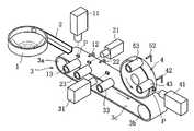
図1はこの実施形態に係る外観検査装置の要部概略構成図であり、1は図示しないホッパから供給される複数の電子部品Pを収容するすり鉢状の容器を備え、遠心力を利用して上記容器内の電子部品Pをその周壁に沿って整列させながら1個ずつ送り出すボールフィーダである。このボールフィーダ1から送り出された電子部品Pは直進(リニア)フィーダ2を介して、第1の搬送機構をなすベルトコンベア機構3上に順次送り出される。
【0011】
ベルトコンベア機構3は、一対のローラ3a,3b間に周回軌道をなして張架されて所定の走行速度で走行駆動される無端状ベルト3cを具備したもので、その上面に前記電子部品Pを載置して一方向に搬送する如く構成される。尚、無端状ベルト3cは、例えば可撓性のスチールベルトの表面にウレタンゴム等を貼付する等して艶消しの黒色表面を有するものからなる。そして後述するカメラによる電子部品Pの撮像時に邪魔となることのない背景をなすように、その仕様が設定されている。またこのベルトコンベア機構3は、上記無端状ベルト3cを横振れ等の振動を招くことなく円滑に走行駆動するべく、例えば前記一対のローラ3a,3b間において凹状のガイド溝を備えたベルト受け(図示せず)上に前記無端状ベルト3cをガイドしながら走行させるように構成される。また前記無端状ベルト3cとしては、その厚み方向の振動を抑えるべく2〜3mm程度の厚みのものが用いられる。
【0012】
しかしてベルトコンベア機構3は電子部品Pを搬送しながら、その搬送路に沿って設けられた第1〜第3の撮像手段(カメラ)11,21,31による該電子部品Pの上面、およびその搬送方向に直交する左右の各側面の撮像に供する役割を担う。即ち、第1のカメラ11はベルトコンベア機構3がなす搬送路の上方に該無端状ベルト3aに対峙させて配置され、無端状ベルト3a上に載置されて搬送される電子部品Pの上面を撮像する如く設けられている。また第2のカメラ21はベルトコンベア機構3の左側部に配置され、無端状ベルト3a上に載置されて搬送される電子部品Pの左側面を撮像するように、更に第3のカメラ31はベルトコンベア機構3の右側部に配置され、無端状ベルト3a上に載置されて搬送される電子部品Pの右側面を撮像するようにそれぞれ設けられている。特にこれらの第1〜第3のカメラ11,21,31は、ベルトコンベア機構3がなす搬送路の上流側からその搬送方向に所定の距離を隔てて順に配置されており、電子部品Pの上面、左側面、そして右側面を順に撮像して外観検査に供するものとなっている。
【0013】
一方、前記ベルトコンベア機構3がなす搬送路の下流側には、その周面を無端状ベルト3aに対峙させて第2の搬送機構としての搬送ドラム4が設けられている。この搬送ドラム4は、その円周面を粘着性を有するシリコーン樹脂等にて構成したもので前記ベルトコンベア機構3に同期して、特に該ベルトコンベア機構3の走行速度と等しい周速度で回転駆動される。そしてこの搬送ドラム4は、無端状ベルト3a上に載置されて搬送されてきた電子部品Pを該無端状ベルト3aとの間に挟み込むことで該電子部品Pの上面にその表面(粘着性を有する円周面)を接触させ、これによって電子部品Pの上面を粘着保持して無端状ベルト3a上から電子部品Pを移し替えて搬送する役割を担う。この搬送ドラム4の表面もまた、電子部品Pの撮像時に邪魔となることのない背景をなすように艶消しの黒色に設定されている。
【0014】
ちなみにベルトコンベア機構3および搬送ドラム4の駆動は、図2に示すように、互いに噛合してモータ5により逆向きに回転駆動される一対の歯車6a,6bを介して、前記ベルトコンベア機構3のプーリ3aと搬送ドラム4とを同時に回転駆動することによって行われる。特にここでは各歯車6a,6bに同軸に設けたプーリ7a,7bと、前記ベルトコンベア機構3のプーリ3aに連接したプーリ8aおよび搬送ドラム4に同軸に設けたプーリ8bとの間にタイミングベルト9a,9bを張架して、互いに同期させて同一周速度で回転駆動する如く構成されている。
【0015】
しかして前記ベルトコンベア機構3の下流側の上方位置であって、前記搬送ドラム4の周面に対向する位置には第4のカメラ41が設けられている。この第4のカメラ41は、その上面を搬送ドラム4の表面に粘着保持されることでその下面側を露呈して搬送される電子部品Pの下面を撮像して外観検査に供するものである。即ち、粘着性の表面(外周面)を有する搬送ドラム4は、微小なチップ状の電子部品Pの上面を粘着保持することで、該電子部品Pの下面を外方に向けて搬送し、その下面を第4のカメラ41による撮像に供するものとなっている。
【0016】
尚、上述した如く第1の搬送機構(ベルトコンベア機構3)および第2の搬送機構(搬送ドラム4)がなす電子部品Pの搬送路に沿って設けられた第1〜第4のカメラ11,21,31,41の各下流側位置には、各カメラ11,21,31,41により外観検査された電子部品P中の不良品を該搬送路上から排除する為のエアノズル12,22,32,42と排出ダクト13,23,33,43とが、該搬送路を挟んでそれぞれ対向配置されている。更に搬送ドラム4の搬送方向下流側(上方位置)には、前記各カメラ11,21,31,41により順次外観検査され、途中で排除されなかった電子部品P、即ち、外観検査に合格した電子部品Pを搬送ドラム4上から排出する為のエアノズル52と排出ダクト53とが対向配置されている。
【0017】
また前記カメラ11,21,31,41による撮像位置の各上流位置、および前記エアノズル12,22,32,42の各上流位置には、図3にその平面配置を示すように、搬送路(無端状ベルト3aおよび搬送ドラム4)の側部に位置して部品検出センサ61,62がそれぞれ設けられている。これらの部品検出センサ61,62は、例えば反射形の光電センサからなり、レーザや赤外線の光ビームを電子部品Pの搬送方向と直角にその搬送路面に沿って照射し、該光ビームの電子部品Pによる反射光を受光する如く構成される。そして反射光の受光により搬送路上での電子部品Pの存在、つまり電子部品Pの搬送に伴うセンシング部位への到達を検出するものとなっている。このような部品検出センサ61,62による電子部品Pの検出タイミングに同期して前記カメラ11,21,31,41による電子部品Pの撮像、また前記エアノズル12,22,32,42の駆動による搬送路上からの電子部品Pの排出がそれぞれ制御される。
【0018】
尚、部品検出センサ61による電子部品Pの検出位置L1は、カメラ11,21,31,41による撮像位置L2とその撮像動作タイミング、および電子部品Pの搬送速度とを考慮して決定される。また同様に部品検出センサ62による電子部品Pの検出位置L3は、エアノズル12,22,32,42による部品排出位置L4とそのエア放出動作タイミング、および電子部品Pの搬送速度とを考慮して決定される。更にカメラ11,21,31,41による撮像位置L2とエアノズル12,22,32,42による部品排出位置L4との関係は、カメラ11,21,31,41により撮像された電子部品Pの各面の画像からの外観検査に要する時間、ひいてはその間に移動する電子部品Pの搬送距離を見込んで設定される。
【0019】
かくして上述した如く構成された外観検査装置においては、ベルトコンベア機構3の無端状ベルト3a上に載置されて搬送される電子部品Pの上面および左右の各側面を第1〜第3のカメラ11,21,31にて順次撮像して各面の外観を検査した後、無端状ベルト3a上の電子部品Pの上面を、粘着性の表面(円周面)を有する搬送ドラム4にて粘着保持して前記無端状ベルト3a上から持ち上げるので、該電子部品Pの下面を簡易に、且つ効果的に露呈させながら搬送ドラム4にて搬送し、第4のカメラ41による撮像に供することができる。この結果、第1の搬送機構(ベルトコンベア機構3)および第2の搬送機構(搬送ドラム4)にて電子部品Pを搬送するだけで、該電子部品Pの主たる外観面である上面と左右の各側面、およびその下面を順次効率的に検査することが可能となる。特に無端状ベルト3a上に供給する電子部品Pの向きを予め定めておくだけで、つまりフィーダ1,2により電子部品Pを整列させてを順次供給するだけで、各カメラ11,21,31,41に対して電子部品Pの向き(姿勢)を格別に制御することなしに、簡易にして効果的にその外観を検査することが可能となる。
【0020】
また前述した[1005]や[0603]と称される微小なチップ状の電子部品(チップ部品)にあっては、その重量自体が極めて軽量であるので、搬送ドラム4の円周面をなすシリコーン樹脂等が持つ程度の粘着性であっても、その上面を十分確実に粘着保持することができる。またこのような搬送ドラム4によれば、エアノズル42,52から或る程度の風量の空気を吹き付けるだけで、その円周面に粘着保持した電子部品Pを容易に剥離することができるので、排出ダクト43,53への払い出しも容易である。従って無端状ベルト3a上から搬送ドラム4への電子部品Pの移し替えが容易であり、また搬送ドラム4上からの電子部品Pの排出も容易なので、電子部品Pを搬送しながらその外観検査を行うことができる。特に従来のようにハンドリング機構を用いて電子部品Pの姿勢を変える等の制御が不要なので、その構成の大幅な簡素化を図ることができる等の実用上多大なる効果が奏せられる。
【0021】
尚、本発明は上述した実施形態に限定されるものではない。例えば無端状ベルト3a上の排出ダクト33の下流側から搬送ドラム4の下面側に向けて、該無端状ベルト3a上に載置されて搬送される電子部品Pの位置ずれを規制するガイド部材を設け、電子部品Pを搬送ドラム4の円周面との間に確実に導くようにしても良い。また搬送ドラム4の表面の粘着性を常に良好に確保するべく、適宜、その表面を清掃するクリーニング機構を組み込むことも有効である。更にこの実施形態においては、第1〜第4のカメラ11,21,31,41による外観検査を通過したものを良品として弁別したが、その良否が曖昧なものを別に弁別するように構成することもできる。この場合には、更に判定不能品を取り出すためのエアノズルと排出ダクトからなる弁別機構を搬送ドラム4の搬送路に沿って設けるようにすれば良い。
【0022】
また搬送ドラム4はその表面に粘着保持した電子部品Pを、円弧軌道を描いて搬送することから、搬送ドラム4の搬送軌道上の特定部位における接線方向に第5および第6のカメラを配置することで、電子部品Pの前端面や後端面についても外観検査するようにし、電子部品Pの6面の全てを検査するように構成することも可能である。更に搬送ドラム4に代えて前記第2の搬送機構として、粘着性の表面を有する可撓性の無端状ベルトを備えたベルトコンベアとして実現することも可能である。
【0023】
更には第2の搬送機構の表面材として、シリコーン樹脂以外の適度な粘着性を有する素材、例えば弱粘着性テープをゴム製の搬送ドラムの表面に張り付けたもの等を用いることも勿論可能である。その他、本発明はその要旨を逸脱しない範囲で種々変形して実施することができる。
【0024】
【発明の効果】
以上説明したように本発明によれば、第1の搬送機構により載置されて搬送されるチップ状の電子部品の上面を、粘着性の表面を有する第2の搬送機構により粘着保持し、これによって該電子部品の下面を露呈させて搬送するので、電子部品の主たる4面をそれぞれ効果的に、しかも簡易に外観検査することができる。特に電子部品の搬送姿勢を格別に制御することなく、所定の向きに整列させて搬送するだけで非常に簡易に外観検査を実行することができ、装置の構成も極めて簡素である等の実用上多大なる効果が奏せられる。
【図面の簡単な説明】
【図1】本発明の一実施形態に係る外観検査装置の要部概略構成図。
【図2】図1に示す外観検査装置における駆動部の構成例を示す図。
【図3】図1に示す外観検査装置におけるカメラとエアノズルおよび排出ダクトの配置関係と、部品検出センサとの位置関係を示す図。
【図4】チップ状の電子部品の外観形状を示す図。
【符号の説明】
P チップ状の電子部品(チップ部品)
1 ボールフィーダ
2 直線(リニア)フィーダ
3 ベルトコンベア機構(第1の搬送機構)
3a 無端状ベルト
4 搬送ドラム(第2の搬送機構)
11 第1のカメラ(撮像手段)
21 第2のカメラ(撮像手段)
31 第3のカメラ(撮像手段)
41 第4のカメラ(撮像手段)[0001]
BACKGROUND OF THE INVENTION
The present invention is a simple and suitable for inspecting the appearance of a minute chip-shaped electronic component (so-called chip component) having a dimension of, for example, 0.3 mm (H) × 0.3 mm (W) × 0.6 mm (L). The present invention relates to an appearance inspection apparatus having a simple structure.
[0002]
[Related background]
Recently, along with the miniaturization and high-density mounting of various electronic circuit units, for example, chip-shaped electronic components having a side of about 3 to 4 mm, so-called chip components, are often used. Particularly recently, for example, a rectangular or substantially rectangular parallelepiped minute electronic component P made of a ceramic resistor or capacitor, specifically, 1.0 mm (L) × referred to as [1005] × Dimensional shape of 0.5mm (H) × 0.5mm (W), and further dimensional shape of 0.6mm (L) × 0.3mm (H) × 0.3mm (W) called [0603] Many small chip parts have been used.
[0003]
By the way, as a technique for assuring the quality of this type of electronic component (chip component), there is a possibility that the function as an electronic component may be damaged due to scratches on the surface, or that the electrode is missing. Inspection is performed from the appearance, and defective products are eliminated prior to supplying parts. Incidentally, in general, in order to inspect the appearance of the above-mentioned small-sized electronic component generally over its six surfaces (upper surface, lower surface, right side surface, left side surface, front end surface, rear end surface), or the
[0004]
[Problems to be solved by the invention]
However, each time a certain surface of the electronic component held by the handling mechanism is imaged by the camera, it takes time to turn the other surface of the electronic component toward the camera, and its posture control and position control are complicated. There is a problem that inspection efficiency is very bad. Furthermore, it is said that it is very difficult to grip the electronic component itself by the handling mechanism or to suck and hold it by the vacuum chuck in the minute electronic component called [0603] described above. There's a problem.
[0005]
In addition, when the appearance inspection is performed continuously at a high speed while sequentially transporting a plurality of electronic components one by one, the handling mechanism is used to hold the electronic components using the handling mechanism or the vacuum chuck in order to change the imaging posture. There is a problem that a high-speed operation of the mechanism and the vacuum chuck and high-precision timing control are required, and the apparatus configuration becomes considerably large. Furthermore, if it is intended to inspect about 1000 to 1500 electronic parts per minute, it will be extremely difficult to realize.
[0006]
The present invention has been made in view of such circumstances, and an object thereof is to provide an appearance inspection apparatus having a simple configuration capable of efficiently inspecting the appearance of a minute chip-shaped electronic component. is there.
[0007]
[Means for Solving the Problems]
In order to achieve the above-described object, the appearance inspection apparatus according to the present invention isan endless shape that carries and drives a chip-shaped electronic component having a substantially rectangular parallelepiped shape on its upper surface, driven in one direction along acircular path. A belt, and first to third imaging means that are provided along the conveying path of the endless belt and that respectively image the upper surface of the electronic component and two side surfaces orthogonal to the conveying direction to provide an appearance inspection; On the downstream side of the conveyance path formed by the endless belt, a circumferential surface forming an adhesive surface is provided opposite to the conveyance surface of the endless belt, and is driven to rotate at a circumferential speed equal to the traveling speed of the endless belt. An electronic component is sandwiched between the endless belt and the upper surface of the electronic component placed on the endless belt is adhered and held, thereby transferring the transfer drum from the endless belt, and the transfer drum. Is characterizedby comprising a fourth imaging means subjecting to image the lower surface of the electronic component to be conveyed to the appearance inspection by.
[0008]
In addition, the visual inspection apparatus according to the present invention further blows air to an electronic component that is determined as a defective product by visual inspection along the conveyance paths formed by the endless belt and the conveyance drum, respectively. An air nozzle that is excluded to the side of the path, and a discharge duct that is disposed opposite to the air nozzle and receives and discharges the electronic component that has been excluded from the transport path.
[0009]
Preferably, the air nozzle is provided on the downstream side of each imaging unit in the transport path in consideration of a time required for an appearance inspection from an image captured by each imaging unit. Moreover, the said conveyance drum is comprised by the silicone resin etc. which have adhesiveness, for example in the surrounding surface so that the upper surface of thesaid electronic component may be stick-held.
[0010]
DETAILED DESCRIPTION OF THE INVENTION
Hereinafter, an embodiment of the present invention will be described with reference to the drawings, taking as an example an appearance inspection apparatus that inspects minute chip-shaped electronic components (chip components) called [1005] and [0603].
FIG. 1 is a schematic configuration diagram of a main part of an appearance inspection apparatus according to this embodiment. Reference numeral 1 includes a mortar-shaped container that houses a plurality of electronic components P supplied from a hopper (not shown), and utilizes centrifugal force. It is a ball feeder which sends out the electronic components P in the container one by one while aligning them along the peripheral wall. The electronic parts P sent out from the ball feeder 1 are sequentially sent out onto a
[0011]
The
[0012]
Thus, while the
[0013]
On the other hand, on the downstream side of the conveying path formed by the
[0014]
Incidentally, as shown in FIG. 2, the
[0015]
Thus, a
[0016]
As described above, the first to
[0017]
Further, at each upstream position of the imaging position by the
[0018]
The detection position L1 of the electronic component P by the
[0019]
Thus, in the visual inspection apparatus configured as described above, the upper and left sides of the electronic component P that is placed on the
[0020]
In addition, the above-mentioned minute chip-shaped electronic components (chip components) called [1005] and [0603] are extremely light in weight, and therefore, silicone forming the circumferential surface of the
[0021]
The present invention is not limited to the embodiment described above. For example, a guide member that regulates the positional deviation of the electronic component P that is placed and conveyed on the
[0022]
Further, since the
[0023]
Furthermore, as a surface material of the second transport mechanism, it is of course possible to use a material having moderate adhesiveness other than silicone resin, such as a material in which a weak adhesive tape is attached to the surface of a rubber transport drum. . In addition, the present invention can be variously modified and implemented without departing from the scope of the invention.
[0024]
【The invention's effect】
As described above, according to the present invention, the upper surface of the chip-like electronic component placed and transported by the first transport mechanism is adhesively held by the second transport mechanism having an adhesive surface, Thus, the lower surface of the electronic component is exposed and conveyed, so that the main four surfaces of the electronic component can be effectively and easily inspected for appearance. In particular, visual control can be performed very simply by aligning and transporting electronic components in a predetermined direction without particularly controlling the transport posture of electronic components, and the configuration of the device is extremely simple. A great effect is produced.
[Brief description of the drawings]
FIG. 1 is a schematic configuration diagram of a main part of an appearance inspection apparatus according to an embodiment of the present invention.
FIG. 2 is a diagram showing a configuration example of a drive unit in the appearance inspection apparatus shown in FIG.
3 is a diagram showing the positional relationship between a camera, an air nozzle, and a discharge duct in the appearance inspection apparatus shown in FIG. 1 and a component detection sensor.
FIG. 4 is a diagram showing an external shape of a chip-shaped electronic component.
[Explanation of symbols]
P Chip-shaped electronic components (chip components)
1
3a
11 First camera (imaging means)
21 Second camera (imaging means)
31 Third camera (imaging means)
41 4th camera (imaging means)
Claims (3)
Translated fromJapaneseこの無端状ベルトの搬送路に沿って設けられて前記電子部品の上面およびその搬送方向と直交する2つの側面をそれぞれ撮像して外観検査に供する第1〜第3の撮像手段と、
前記無端状ベルトがなす搬送路の下流側において、粘着面をなす周面を前記無端状ベルトの搬送面に対峙させて設けられ、前記無端状ベルトの走行速度と等しい周速度で回転駆動されて前記無端状ベルトとの間に電子部品を挟み込み、前記無端状ベルトに載置された電子部品の上面を粘着保持することで前記無端状ベルト上から移し替えて搬送する搬送ドラムと、
この搬送ドラムにより搬送される電子部品の下面を撮像して外観検査に供する第4の撮像手段と
を具備したことを特徴とする外観検査装置。An endless belt that travels in one direction on a circular path and carries and transports chip-shaped electronic components having a substantially rectangular parallelepiped shape on the upper surface thereof;
First to third imaging means that are provided along the conveying path of the endless belt and image the upper surface of the electronic component and two side surfaces orthogonal to the conveying direction, respectively, and provide for an appearance inspection;
On the downstream side of the conveyance path formed by the endless belt, a circumferential surface forming an adhesive surface is provided opposite to the conveyance surface of the endless belt, and is driven to rotate at a circumferential speed equal to the traveling speed of the endless belt. A transport drum that sandwiches an electronic component between the endless belt and transfers and transports the electronic component mounted on the endless belt by sticking and holding the upper surface of the electronic component;
An appearance inspection apparatus, comprising: afourth image pickup means for picking upan image of the lower surface of the electronic component conveyed by the conveyance drum and for use in appearance inspection.
更に前記無端状ベルトおよび前記搬送ドラムがそれぞれなす搬送路に沿って、外観検査により不良品として判定された電子部品に空気を吹き付けて該電子部品を前記搬送路の側方に排除するエアノズルと、このエアノズルに対向配置されて前記搬送路から排除された電子部品を受け止めて排出する排出ダクトとを備えることを特徴とする外観検査装置。The appearance inspection apparatus according to claim 1,
Furthermore, air nozzles that blow air to electronic parts that are determined as defective products by visual inspection along the conveyance paths formed by the endless belt and the conveyance drum, respectively, to exclude the electronic parts to the side of the conveyance path; An appearance inspection apparatus comprising:a discharge duct arranged to face the air nozzle and receiving and discharging an electronic component excluded from the conveyance path .
Priority Applications (1)
| Application Number | Priority Date | Filing Date | Title |
|---|---|---|---|
| JP15103399AJP4251307B2 (en) | 1999-05-31 | 1999-05-31 | Appearance inspection device |
Applications Claiming Priority (1)
| Application Number | Priority Date | Filing Date | Title |
|---|---|---|---|
| JP15103399AJP4251307B2 (en) | 1999-05-31 | 1999-05-31 | Appearance inspection device |
Publications (2)
| Publication Number | Publication Date |
|---|---|
| JP2000337843A JP2000337843A (en) | 2000-12-08 |
| JP4251307B2true JP4251307B2 (en) | 2009-04-08 |
Family
ID=15509843
Family Applications (1)
| Application Number | Title | Priority Date | Filing Date |
|---|---|---|---|
| JP15103399AExpired - LifetimeJP4251307B2 (en) | 1999-05-31 | 1999-05-31 | Appearance inspection device |
Country Status (1)
| Country | Link |
|---|---|
| JP (1) | JP4251307B2 (en) |
Families Citing this family (8)
| Publication number | Priority date | Publication date | Assignee | Title |
|---|---|---|---|---|
| KR100453291B1 (en)* | 2002-06-05 | 2004-10-15 | (주)화인 | Apparatus for inspecting of chip equipped steel belt and the same method |
| CN1968876B (en) | 2004-04-13 | 2012-10-31 | Tdk株式会社 | Chip parts transfer device and visual inspection device |
| JP5555839B1 (en) | 2013-09-02 | 2014-07-23 | 上野精機株式会社 | Appearance inspection device |
| US9731328B2 (en) | 2015-08-03 | 2017-08-15 | Linear Group Services, LLC | Inspection and sorting machine |
| CN108195844B (en)* | 2018-01-19 | 2024-05-03 | 苏州杰锐思智能科技股份有限公司 | Cylinder outward appearance detection module |
| CN113353541B (en)* | 2021-06-29 | 2023-03-03 | 红云红河烟草(集团)有限责任公司 | Automatic deviation rectifying system of belt conveyor belt |
| CN115468516B (en)* | 2022-09-22 | 2024-03-26 | 苏州襄行智能科技有限公司 | Cuboid precision six-surface measuring machine |
| CN117233172A (en)* | 2023-11-16 | 2023-12-15 | 河南柏科沃电子科技有限公司 | Intelligent capacitor detection device and detection method |
- 1999
- 1999-05-31JPJP15103399Apatent/JP4251307B2/ennot_activeExpired - Lifetime
Also Published As
| Publication number | Publication date |
|---|---|
| JP2000337843A (en) | 2000-12-08 |
Similar Documents
| Publication | Publication Date | Title |
|---|---|---|
| JP4039505B2 (en) | Appearance inspection device | |
| US6601365B2 (en) | Component handling apparatus and method of handling the same | |
| JP2585133B2 (en) | Parts appearance sorting device | |
| WO2005100215A1 (en) | Chip component carrying method and system, and visual inspection method and system | |
| US8302290B2 (en) | Apparatus for mounting electronic parts | |
| JP2009208963A (en) | Conveyor reversing device, and inspection device using the same | |
| WO2001038013A1 (en) | Work inspection device | |
| JP2008105811A (en) | Work appearance inspection device | |
| JP4251307B2 (en) | Appearance inspection device | |
| JPH08168727A (en) | Apparatus for inspecting small articles | |
| WO2024082758A1 (en) | Assembly and production line | |
| JPH0565405B2 (en) | ||
| JP5183979B2 (en) | Work inspection equipment | |
| JP2004345859A (en) | Chip part conveyance method, its device, appearance inspection method, and its device | |
| JP4883510B2 (en) | Conveyor reversing device and inspection device using the same | |
| JP2004045097A (en) | Appearance inspection device | |
| JP3553832B2 (en) | Transfer device, inspection device and alignment supply device | |
| JPH0834759B2 (en) | Conveyed object inspection method and apparatus | |
| JP2004010254A (en) | Conveying device | |
| JPH0432355Y2 (en) | ||
| JP2852646B2 (en) | Tracking system | |
| JPS61212374A (en) | Conveyor | |
| JP3414056B2 (en) | Marking device | |
| JPH10185824A (en) | Device for inspecting small product and method using the device | |
| JP3425101B2 (en) | Holding and conveying device and inspection device for lightweight articles |
Legal Events
| Date | Code | Title | Description |
|---|---|---|---|
| A621 | Written request for application examination | Free format text:JAPANESE INTERMEDIATE CODE: A621 Effective date:20060526 | |
| A131 | Notification of reasons for refusal | Free format text:JAPANESE INTERMEDIATE CODE: A131 Effective date:20081008 | |
| A521 | Written amendment | Free format text:JAPANESE INTERMEDIATE CODE: A523 Effective date:20081104 | |
| TRDD | Decision of grant or rejection written | ||
| A01 | Written decision to grant a patent or to grant a registration (utility model) | Free format text:JAPANESE INTERMEDIATE CODE: A01 Effective date:20081210 | |
| A01 | Written decision to grant a patent or to grant a registration (utility model) | Free format text:JAPANESE INTERMEDIATE CODE: A01 | |
| RD01 | Notification of change of attorney | Free format text:JAPANESE INTERMEDIATE CODE: A7426 Effective date:20090108 | |
| A61 | First payment of annual fees (during grant procedure) | Free format text:JAPANESE INTERMEDIATE CODE: A61 Effective date:20090108 | |
| R150 | Certificate of patent or registration of utility model | Ref document number:4251307 Country of ref document:JP Free format text:JAPANESE INTERMEDIATE CODE: R150 Free format text:JAPANESE INTERMEDIATE CODE: R150 | |
| FPAY | Renewal fee payment (event date is renewal date of database) | Free format text:PAYMENT UNTIL: 20120130 Year of fee payment:3 | |
| FPAY | Renewal fee payment (event date is renewal date of database) | Free format text:PAYMENT UNTIL: 20150130 Year of fee payment:6 | |
| R250 | Receipt of annual fees | Free format text:JAPANESE INTERMEDIATE CODE: R250 | |
| R250 | Receipt of annual fees | Free format text:JAPANESE INTERMEDIATE CODE: R250 | |
| R250 | Receipt of annual fees | Free format text:JAPANESE INTERMEDIATE CODE: R250 | |
| EXPY | Cancellation because of completion of term |