JP4249679B2 - Electrophotographic photosensitive member, image forming apparatus, and process cartridge for image forming apparatus - Google Patents
Electrophotographic photosensitive member, image forming apparatus, and process cartridge for image forming apparatusDownload PDFInfo
- Publication number
- JP4249679B2 JP4249679B2JP2004256032AJP2004256032AJP4249679B2JP 4249679 B2JP4249679 B2JP 4249679B2JP 2004256032 AJP2004256032 AJP 2004256032AJP 2004256032 AJP2004256032 AJP 2004256032AJP 4249679 B2JP4249679 B2JP 4249679B2
- Authority
- JP
- Japan
- Prior art keywords
- group
- charge transport
- photosensitive member
- electrophotographic photosensitive
- transport layer
- Prior art date
- Legal status (The legal status is an assumption and is not a legal conclusion. Google has not performed a legal analysis and makes no representation as to the accuracy of the status listed.)
- Expired - Fee Related
Links
Images


Classifications
- G—PHYSICS
- G03—PHOTOGRAPHY; CINEMATOGRAPHY; ANALOGOUS TECHNIQUES USING WAVES OTHER THAN OPTICAL WAVES; ELECTROGRAPHY; HOLOGRAPHY
- G03G—ELECTROGRAPHY; ELECTROPHOTOGRAPHY; MAGNETOGRAPHY
- G03G5/00—Recording members for original recording by exposure, e.g. to light, to heat, to electrons; Manufacture thereof; Selection of materials therefor
- G03G5/02—Charge-receiving layers
- G03G5/04—Photoconductive layers; Charge-generation layers or charge-transporting layers; Additives therefor; Binders therefor
- G03G5/05—Organic bonding materials; Methods for coating a substrate with a photoconductive layer; Inert supplements for use in photoconductive layers
- G03G5/0528—Macromolecular bonding materials
- G03G5/0592—Macromolecular compounds characterised by their structure or by their chemical properties, e.g. block polymers, reticulated polymers, molecular weight, acidity
- G—PHYSICS
- G03—PHOTOGRAPHY; CINEMATOGRAPHY; ANALOGOUS TECHNIQUES USING WAVES OTHER THAN OPTICAL WAVES; ELECTROGRAPHY; HOLOGRAPHY
- G03G—ELECTROGRAPHY; ELECTROPHOTOGRAPHY; MAGNETOGRAPHY
- G03G5/00—Recording members for original recording by exposure, e.g. to light, to heat, to electrons; Manufacture thereof; Selection of materials therefor
- G03G5/02—Charge-receiving layers
- G03G5/04—Photoconductive layers; Charge-generation layers or charge-transporting layers; Additives therefor; Binders therefor
- G03G5/05—Organic bonding materials; Methods for coating a substrate with a photoconductive layer; Inert supplements for use in photoconductive layers
- G03G5/0528—Macromolecular bonding materials
- G03G5/0532—Macromolecular bonding materials obtained by reactions only involving carbon-to-carbon unsatured bonds
- G03G5/0546—Polymers comprising at least one carboxyl radical, e.g. polyacrylic acid, polycrotonic acid, polymaleic acid; Derivatives thereof, e.g. their esters, salts, anhydrides, nitriles, amides
- G—PHYSICS
- G03—PHOTOGRAPHY; CINEMATOGRAPHY; ANALOGOUS TECHNIQUES USING WAVES OTHER THAN OPTICAL WAVES; ELECTROGRAPHY; HOLOGRAPHY
- G03G—ELECTROGRAPHY; ELECTROPHOTOGRAPHY; MAGNETOGRAPHY
- G03G5/00—Recording members for original recording by exposure, e.g. to light, to heat, to electrons; Manufacture thereof; Selection of materials therefor
- G03G5/02—Charge-receiving layers
- G03G5/04—Photoconductive layers; Charge-generation layers or charge-transporting layers; Additives therefor; Binders therefor
- G03G5/05—Organic bonding materials; Methods for coating a substrate with a photoconductive layer; Inert supplements for use in photoconductive layers
- G03G5/0528—Macromolecular bonding materials
- G03G5/0589—Macromolecular compounds characterised by specific side-chain substituents or end groups
- G—PHYSICS
- G03—PHOTOGRAPHY; CINEMATOGRAPHY; ANALOGOUS TECHNIQUES USING WAVES OTHER THAN OPTICAL WAVES; ELECTROGRAPHY; HOLOGRAPHY
- G03G—ELECTROGRAPHY; ELECTROPHOTOGRAPHY; MAGNETOGRAPHY
- G03G5/00—Recording members for original recording by exposure, e.g. to light, to heat, to electrons; Manufacture thereof; Selection of materials therefor
- G03G5/02—Charge-receiving layers
- G03G5/04—Photoconductive layers; Charge-generation layers or charge-transporting layers; Additives therefor; Binders therefor
- G03G5/06—Photoconductive layers; Charge-generation layers or charge-transporting layers; Additives therefor; Binders therefor characterised by the photoconductive material being organic
- G03G5/0664—Dyes
- G03G5/0696—Phthalocyanines
- G—PHYSICS
- G03—PHOTOGRAPHY; CINEMATOGRAPHY; ANALOGOUS TECHNIQUES USING WAVES OTHER THAN OPTICAL WAVES; ELECTROGRAPHY; HOLOGRAPHY
- G03G—ELECTROGRAPHY; ELECTROPHOTOGRAPHY; MAGNETOGRAPHY
- G03G5/00—Recording members for original recording by exposure, e.g. to light, to heat, to electrons; Manufacture thereof; Selection of materials therefor
- G03G5/02—Charge-receiving layers
- G03G5/04—Photoconductive layers; Charge-generation layers or charge-transporting layers; Additives therefor; Binders therefor
- G03G5/06—Photoconductive layers; Charge-generation layers or charge-transporting layers; Additives therefor; Binders therefor characterised by the photoconductive material being organic
- G03G5/07—Polymeric photoconductive materials
- G03G5/071—Polymeric photoconductive materials obtained by reactions only involving carbon-to-carbon unsaturated bonds
- G03G5/072—Polymeric photoconductive materials obtained by reactions only involving carbon-to-carbon unsaturated bonds comprising pending monoamine groups
- G03G5/0732—Polymeric photoconductive materials obtained by reactions only involving carbon-to-carbon unsaturated bonds comprising pending monoamine groups comprising pending alkenylarylamine
- G—PHYSICS
- G03—PHOTOGRAPHY; CINEMATOGRAPHY; ANALOGOUS TECHNIQUES USING WAVES OTHER THAN OPTICAL WAVES; ELECTROGRAPHY; HOLOGRAPHY
- G03G—ELECTROGRAPHY; ELECTROPHOTOGRAPHY; MAGNETOGRAPHY
- G03G5/00—Recording members for original recording by exposure, e.g. to light, to heat, to electrons; Manufacture thereof; Selection of materials therefor
- G03G5/02—Charge-receiving layers
- G03G5/04—Photoconductive layers; Charge-generation layers or charge-transporting layers; Additives therefor; Binders therefor
- G03G5/06—Photoconductive layers; Charge-generation layers or charge-transporting layers; Additives therefor; Binders therefor characterised by the photoconductive material being organic
- G03G5/07—Polymeric photoconductive materials
- G03G5/071—Polymeric photoconductive materials obtained by reactions only involving carbon-to-carbon unsaturated bonds
- G03G5/074—Polymeric photoconductive materials obtained by reactions only involving carbon-to-carbon unsaturated bonds comprising pending diamine
- G—PHYSICS
- G03—PHOTOGRAPHY; CINEMATOGRAPHY; ANALOGOUS TECHNIQUES USING WAVES OTHER THAN OPTICAL WAVES; ELECTROGRAPHY; HOLOGRAPHY
- G03G—ELECTROGRAPHY; ELECTROPHOTOGRAPHY; MAGNETOGRAPHY
- G03G5/00—Recording members for original recording by exposure, e.g. to light, to heat, to electrons; Manufacture thereof; Selection of materials therefor
- G03G5/02—Charge-receiving layers
- G03G5/04—Photoconductive layers; Charge-generation layers or charge-transporting layers; Additives therefor; Binders therefor
- G03G5/06—Photoconductive layers; Charge-generation layers or charge-transporting layers; Additives therefor; Binders therefor characterised by the photoconductive material being organic
- G03G5/07—Polymeric photoconductive materials
- G03G5/071—Polymeric photoconductive materials obtained by reactions only involving carbon-to-carbon unsaturated bonds
- G03G5/0745—Polymeric photoconductive materials obtained by reactions only involving carbon-to-carbon unsaturated bonds comprising pending hydrazone
Landscapes
- Physics & Mathematics (AREA)
- General Physics & Mathematics (AREA)
- Chemical & Material Sciences (AREA)
- Chemical Kinetics & Catalysis (AREA)
- Spectroscopy & Molecular Physics (AREA)
- Photoreceptors In Electrophotography (AREA)
Description
Translated fromJapanese本発明は、感光層に少なくとも平均粒子サイズが0.25μm以下である特定の結晶型を有するチタニルフタロシアニン結晶を含有する電荷発生層と電荷輸送層、さらに架橋型電荷輸送層を順に積層してなる電子写真感光体、これを用いた画像形成方法、画像形成装置ならびに画像形成装置用プロセスカートリッジに関する。 In the present invention, a charge generation layer containing a titanyl phthalocyanine crystal having a specific crystal type having an average particle size of 0.25 μm or less, a charge transport layer, and a crosslinked charge transport layer are sequentially laminated on the photosensitive layer. The present invention relates to an electrophotographic photosensitive member, an image forming method using the same, an image forming apparatus, and a process cartridge for the image forming apparatus.
近年、電子写真方式を用いた情報処理システム機の発展は目覚ましく、特に情報をデジタル信号に変換して光によって情報記録を行なうレーザープリンタやデジタル複写機は、そのプリント品質、信頼性において向上が著しい。急速に普及しているこれらのレーザープリンタやデジタル複写機は、今後高画質化と同時にさらなる高速化あるいは小型化が要求されている。
さらに、最近ではフルカラープリントが可能なフルカラーレーザープリンタやフルカラーデジタル複写機の需要も急激に高くなっている。フルカラープリントを行なう場合には、少なくとも4色のトナー画像を重ね合わせる必要があることから、特に装置の高速化並びに小型化がより一層重要な課題とされている。装置の高速化及び小型化を実現するためには、それらに用いられる電子写真感光体の感度を向上させるとともに感光体の小径化が必要となる。
しかし、その場合感光体は、より過酷な状況で使用されることになるため、従来の感光体ではその交換速度が大幅に早まることになる。従って、装置の高速化並びに小型化を実現するためには、同時に用いられる感光体の高耐久化あるいは高安定化が必要不可欠である。
感光体の耐久性は、画像品質によって決定され、特に反転現像によるレーザープリンタやデジタル複写機では、白地に無数の黒点が印字される地肌汚れが寿命を決める最大の要因とされている。
従って、装置の高速化及び小型化を実現するためには、感光体の高感度化と同時に地肌汚れの発生を抑制し、感光体の高寿命化を実現する必要がある。In recent years, the development of information processing systems using electrophotography has been remarkable, and laser printers and digital copiers that record information using light by converting information into digital signals have significantly improved print quality and reliability. . These laser printers and digital copiers that are rapidly spreading are required to have higher speed and smaller size as well as higher image quality.
Furthermore, recently, the demand for full-color laser printers and full-color digital copiers capable of full-color printing is rapidly increasing. In the case of performing full color printing, it is necessary to superimpose toner images of at least four colors, and in particular, speeding up and downsizing of the apparatus are even more important issues. In order to realize high speed and downsizing of the apparatus, it is necessary to improve the sensitivity of the electrophotographic photosensitive member used for them and to reduce the diameter of the photosensitive member.
However, in this case, since the photoconductor is used in a severer situation, the replacement speed of the conventional photoconductor is greatly increased. Therefore, in order to realize high speed and downsizing of the apparatus, it is indispensable to make the photoconductor used at the same time highly durable or highly stable.
The durability of the photoreceptor is determined by the image quality. In particular, in laser printers and digital copiers using reversal development, background stains with countless black spots printed on a white background are the largest factors that determine the service life.
Therefore, in order to realize high speed and downsizing of the apparatus, it is necessary to increase the life of the photoconductor by suppressing the occurrence of background stains at the same time as increasing the sensitivity of the photoconductor.
装置の高速化に対応するために必要な感光体の高感度化に対しては、量子効率の大きな電荷発生材料が必要不可欠である。
有機系高感度感光体としては、電荷発生材料にXRD(CuKα線(波長1.542Å)におけるブラッグ角2θの回折ピーク(±0.2゜)が、少なくとも27.2゜に最大回折ピークを有するチタニルフタロシアニンが広く用いられており、非常に有効である。
しかし、上記チタニルフタロシアニンを用いた感光体は、顔料の凝集や疲労による帯電低下等によって地肌汚れが顕著に発生する懸念があった。特に、地肌汚れは前述のとおり感光体の寿命を決定する大きな要因であり、上記チタニルフタロシアニンを用いた感光体は装置の高速化が可能となっても地肌汚れの影響が大きくなるために、画質安定性に乏しく、高速化と高寿命化の両立が実現されていなかった(例えば、特許文献1参照)。
そのため、上記チタニルフタロシアニンを用いた従来の感光体は、高速機に用いると感光体の交換頻度が早くなり、安定した画像を長期に渡って提供することが実現できていなかった。A charge generating material having a high quantum efficiency is indispensable for increasing the sensitivity of the photoreceptor required to cope with the higher speed of the apparatus.
As an organic high-sensitivity photoreceptor, the charge generation material has a XRD (CuKα ray (wavelength: 1.542 mm) Bragg angle 2θ diffraction peak (± 0.2 °), and a maximum diffraction peak of at least 27.2 °. Titanyl phthalocyanine is widely used and very effective.
However, the photoconductor using the above titanyl phthalocyanine has a concern that background stains may be remarkably generated due to aggregation of pigments or reduction in charge due to fatigue. In particular, background contamination is a major factor that determines the life of a photoconductor as described above, and a photoconductor using the above-mentioned titanyl phthalocyanine increases the influence of background contamination even if the speed of the apparatus can be increased. The stability is poor, and both high speed and long life have not been realized (see, for example, Patent Document 1).
For this reason, when the conventional photoconductor using the titanyl phthalocyanine is used in a high-speed machine, the frequency of replacement of the photoconductor is increased, and it has not been possible to provide a stable image over a long period of time.
一方、電子写真感光体の高寿命化に対しては、感光体表面に保護層を形成し耐摩耗性を高める方法が知られている。感光体の寿命を決める地肌汚れは、繰り返し使用による感光体の疲労あるいは摩耗によって促進される。感光体表面に保護層を形成することによって、繰り返し使用による感光体の摩耗を抑制することは、それによって起こる電界強度の増加を抑制できることから地肌汚れの発生を軽減することが可能であり、高寿命化に対し非常に有効な手段である。 On the other hand, in order to increase the life of an electrophotographic photoreceptor, a method is known in which a protective layer is formed on the surface of the photoreceptor to increase the wear resistance. Background contamination that determines the life of the photoreceptor is promoted by fatigue or wear of the photoreceptor due to repeated use. By forming a protective layer on the surface of the photoconductor, suppressing wear of the photoconductor due to repeated use can suppress an increase in the electric field strength caused by the use, thereby reducing the occurrence of background stains. This is a very effective means for extending the service life.
感光層の耐摩耗性を改良する技術としては、(i)架橋型電荷輸送層に硬化性バインダーを用いたもの(例えば、特許文献2参照)、(ii)高分子型電荷輸送物質を用いたもの(例えば、特許文献3参照)、(iii)架橋型電荷輸送層に無機フィラーを分散させたもの(例えば、特許文献4参照)等が挙げられる。これらの技術の内、(i)の硬化性バインダーを用いたものは、電荷輸送物質との相溶性が悪いためや重合開始剤、未反応残基などの不純物により残留電位が上昇し画像濃度低下が発生し易い傾向がある。また、(ii)の高分子型電荷輸送物質を用いたものは、ある程度の耐摩耗性向上が可能であるものの、有機感光体に求められている耐久性を十二分に満足させるまでには至っていない。また、高分子型電荷輸送物質は材料の重合、精製が難しく高純度なものが得にくいため材料間の電気的特性が安定しにくい。更に塗工液が高粘度となる等の製造上の問題を起こす場合もある。(iii)の無機フィラーを分散させたものは、通常の低分子電荷輸送物質を不活性高分子に分散させた感光体に比べ高い耐摩耗性が発揮されるが、無機フィラー表面に存在する電荷トラップにより残留電位が上昇し、画像濃度低下が発生し易い傾向にある。また、感光体表面の無機フィラーとバインター樹脂の凹凸が大きい場合には、クリーニング不良が発生し、トナーフィルミングや画像流れの原因となることがある。これら(i)、(ii)、(iii)の技術では、有機感光体に求められる電気的な耐久性、機械的な耐久性をも含めた総合的な耐久性を十二分に満足するには至っていない。 Techniques for improving the abrasion resistance of the photosensitive layer include (i) using a curable binder in the crosslinkable charge transport layer (see, for example, Patent Document 2), and (ii) using a polymer charge transport material. (For example, refer to Patent Document 3), and (iii) a structure in which an inorganic filler is dispersed in a crosslinked charge transport layer (for example, refer to Patent Document 4). Among these technologies, those using the curable binder (i) have poor compatibility with the charge transport material, and the residual potential increases due to impurities such as polymerization initiators and unreacted residues, resulting in a decrease in image density. Tends to occur. In addition, although the polymer type charge transport material (ii) can improve the abrasion resistance to some extent, the durability required for the organic photoreceptor is not fully satisfied. Not reached. In addition, polymer charge transport materials are difficult to polymerize and purify, and it is difficult to obtain a high-purity material. Therefore, it is difficult to stabilize electrical characteristics between materials. Furthermore, production problems such as high viscosity of the coating solution may occur. The dispersion of the inorganic filler (iii) exhibits higher abrasion resistance than a photoreceptor in which a normal low molecular charge transport material is dispersed in an inert polymer, but the charge present on the surface of the inorganic filler. The residual potential increases due to the trap, and the image density tends to decrease. In addition, when the unevenness of the inorganic filler and the binder resin on the surface of the photoconductor is large, defective cleaning may occur, which may cause toner filming and image flow. With the technologies (i), (ii), and (iii), the total durability including the electrical durability and mechanical durability required for the organic photoreceptor is sufficiently satisfied. Has not reached.
更に、(i)の耐摩耗性と耐傷性を改良するために多官能のアクリレートモノマー硬化物を含有させた感光体も知られている(特許文献5参照)。しかし、この感光体においては、感光層上に設けた保護層にこの多官能のアクリレートモノマー硬化物を含有させる旨の記載があるものの、この保護層においては電荷輸送物質を含有せしめてもよいことが記載されているのみで具体的な記載はなく、しかも、単に架橋型電荷輸送層に低分子の電荷輸送物質を含有させた場合には、上記硬化物との相溶性の問題があり、これにより、低分子電荷輸送物質の析出、白濁現象が起こり、露光部電位の上昇により画像濃度が低下するばかりでなく機械強度も低下してしまうことがあった。
さらに、この感光体は、具体的には高分子バインダーを含有した状態でモノマーを反応させるため、3次元網目構造が充分に進行せず、架橋結合密度が希薄となるため飛躍的な耐摩耗性を発揮できるまでには至っていない。Furthermore, a photoreceptor containing a polyfunctional acrylate monomer cured product for improving the abrasion resistance and scratch resistance of (i) is also known (see Patent Document 5). However, in this photoreceptor, although there is a description that the polyfunctional acrylate monomer cured product is contained in the protective layer provided on the photosensitive layer, the protective layer may contain a charge transport material. However, there is a problem of compatibility with the cured product when a low-molecular charge transport material is simply contained in the cross-linked charge transport layer. As a result, precipitation of a low-molecular charge transport material and white turbidity occur, and not only the image density is lowered but also the mechanical strength is lowered due to an increase in the exposed area potential.
Furthermore, since this photoconductor specifically reacts with the monomer in a state containing a polymer binder, the three-dimensional network structure does not proceed sufficiently, and the crosslink density becomes dilute, resulting in a dramatic wear resistance. Has not yet been able to demonstrate.
これらに換わる感光層の耐摩耗技術として、炭素−炭素二重結合を有するモノマーと、炭素−炭素二重結合を有する電荷輸送物質及びバインダー樹脂からなる塗工液を用いて形成した電荷輸送層を設けることが知られている(例えば、特許文献6参照)。このバインダー樹脂は電荷発生層と架橋型電荷輸送層の接着性を向上させ、さらに厚膜硬化時の膜の内部応力を緩和させる役割を果たしていると考えられ、炭素−炭素二重結合を有し、上記電荷輸送物質に対して反応性を有するものと、上記二重結合を有せず反応性を有しないものに大別される。この感光体は耐摩耗性と良好な電気的特性を両立しており注目されるが、バインダー樹脂として反応性を有しないものを使用した場合においては、バインダー樹脂と、上記モノマーと電荷輸送物質との反応により生成した硬化物との相溶性が悪く、架橋型電荷輸送層中で層分離が生じ、傷やトナー中の外添剤及び紙粉の固着の原因となることがある。また、上記したように、3次元網目構造が充分に進行せず、架橋結合密度が希薄となるため飛躍的な耐摩耗性を発揮できるまでには至っていない。加えて、この感光体において使用される上記モノマーとして具体的に記載されているものは2官能性のものであり、これらの点で耐摩耗性の点では未だ満足するには至らなかった。また、反応性を有するバインダーを使用した場合においても、硬化物の分子量は増大するものの分子間架橋結合数は少なく、上記電荷輸送物質の結合量と架橋密度との両立は難しく、電気特性及び耐摩耗性も充分とはいえないものであった。 As a wear resistance technique for a photosensitive layer that replaces these, a charge transport layer formed by using a coating solution comprising a monomer having a carbon-carbon double bond, a charge transport material having a carbon-carbon double bond, and a binder resin. It is known to provide (for example, refer to Patent Document 6). This binder resin is thought to play a role of improving the adhesion between the charge generation layer and the cross-linked charge transport layer, and also relaxing the internal stress of the film during thick film curing, and has a carbon-carbon double bond. These are roughly classified into those having reactivity with the charge transporting substance and those having no reactivity with the double bond. This photoconductor is remarkably compatible with wear resistance and good electrical properties. However, when a non-reactive binder resin is used, the binder resin, the monomer, and the charge transport material are used. The compatibility with the cured product produced by this reaction is poor, and layer separation occurs in the cross-linked charge transport layer, which may cause scratches and sticking of external additives and paper powder in the toner. In addition, as described above, the three-dimensional network structure does not proceed sufficiently, and the cross-linking density becomes dilute. In addition, what is specifically described as the monomer used in this photoreceptor is bifunctional, and in these respects, it has not yet been satisfactory in terms of wear resistance. Even when a reactive binder is used, the molecular weight of the cured product is increased, but the number of intermolecular crosslinks is small, and it is difficult to achieve a balance between the amount of the charge transporting substance and the crosslink density. Abrasion was not sufficient.
また、同一分子内に二つ以上の連鎖重合性官能基を有する正孔輸送性化合物を硬化した化合物を含有する感光層も知られている(例えば、特許文献7参照)。この感光層は架橋結合密度を高められるため高い硬度を有するが、嵩高い正孔輸送性化合物が二つ以上の連鎖重合性官能基を有するため硬化物中に歪みが発生し内部応力が高くなり、架橋表面層が長期間の使用においてクラックや剥がれが発生しやすい場合がある。
これら従来技術における電荷輸送性構造を化学結合させた架橋感光層を有する感光体においても、現状では充分な総合特性を有しているとは言えない。A photosensitive layer containing a compound obtained by curing a hole transporting compound having two or more chain polymerizable functional groups in the same molecule is also known (see, for example, Patent Document 7). This photosensitive layer has high hardness because the crosslink density can be increased, but since the bulky hole transporting compound has two or more chain polymerizable functional groups, distortion occurs in the cured product and internal stress increases. In some cases, the crosslinked surface layer is liable to crack or peel off when used for a long period of time.
Even in these conventional techniques, a photoreceptor having a crosslinked photosensitive layer in which a charge transporting structure is chemically bonded cannot be said to have sufficient comprehensive characteristics at present.
このように、電荷発生層に高感度を有する上記チタニルフタロシアニンを含む感光体を用いることによって、装置の高速化に対応できたとしても、地肌汚れの発生により画質低下が見られ感光体を頻繁に交換する必要が生じたり、保護層を形成して耐摩耗性の向上が可能となっても、残留電位上昇やクリーニング不良による画質劣化等の影響が増大したりして、高速機やカラー機に要求される感光体の高感度化と高寿命化の両立が実現できていなかった。従って、近年のレーザープリンタやデジタル複写機における高速化あるいはカラー化の要求に対し、安定した画像を長期に渡って出力可能な電子写真感光体並びに画像形成装置が強く求められていた。 As described above, even when the device can cope with speeding up of the apparatus by using the photoconductor including the titanyl phthalocyanine having high sensitivity in the charge generation layer, the image quality is deteriorated due to the occurrence of background contamination, and the photoconductor is frequently used. Even if it is necessary to replace it, or a protective layer is formed to improve wear resistance, the effects of increased residual potential and image quality degradation due to poor cleaning may increase, resulting in high speed and color machines. It has not been possible to achieve both the required high sensitivity and long life of the photoreceptor. Accordingly, there has been a strong demand for an electrophotographic photosensitive member and an image forming apparatus capable of outputting a stable image over a long period of time in response to the recent demand for high speed or colorization in laser printers and digital copying machines.
本発明の目的は、装置の高速化、カラー化あるいは小型化に対応するため、高感度を有しかつ繰り返し使用しても画質安定性が高く、高寿命を有する電子写真感光体、並びにそれを用いた画像形成装置及び画像形成装置用プロセスカートリッジを提供することにある。 An object of the present invention is to cope with speeding up, colorization and miniaturization of an apparatus, and an electrophotographic photosensitive member having high sensitivity, high image stability even when used repeatedly, and having a long life, and the same To provide an image forming apparatus and a process cartridge for the image forming apparatus used.
本発明者らは、高速対応が可能であり、かつ繰り返し使用に対しても画質安定性が高く、さらに高寿命を有する電子写真感光体を得るために鋭意検討を行なった結果、以下の構成を満たすことにより達成可能であることを見い出し、本発明を完成するに至った。 As a result of intensive investigations to obtain an electrophotographic photosensitive member capable of high-speed correspondence, high image quality stability even with repeated use, and having a long life, the following configuration is obtained. It has been found that it can be achieved by satisfying the requirements, and the present invention has been completed.
上記課題は、本発明の(1)「少なくとも導電性支持体上に電荷発生層、電荷輸送層及び架橋型電荷輸送層を順次積層した電子写真感光体において、該電荷発生層中にCuKα線(波長1.542Å)に対するブラッグ角2θの回折ピーク(±0.2゜)として、少なくとも27.2゜に最大回折ピークを有し、更に9.4゜、9.6゜、24.0゜に主要なピークを有し、かつ最も低角側の回折ピークとして7.3゜にピークを有し、7.3°のピークと9.4°のピークの間にピークを有さず、更に26.3°にピークを有さず、一次粒子の平均粒子サイズが0.25μm以下であるチタニルフタロシアニン結晶粒子を含み、該架橋型電荷輸送層が少なくとも電荷輸送性構造を有しない3官能以上のラジカル重合性モノマーと1官能の電荷輸送性構造を有するラジカル重合性化合物を硬化することにより形成され、該架橋型電荷輸送層の膜厚が1μm以上、10μm以下であることを特徴とする電子写真感光体」、(2)「前記チタニルフタロシアニン結晶粒子の体積平均粒径が0.3μm以下で、その標準偏差が0.2μm以下になるまで分散を行い、その後有効孔径が3μm以下のフィルターにて濾過を行なった分散液を使用し、感光層あるいは電荷発生層を塗工したことを特徴とする前記第(1)項に記載の電子写真感光体」、(3)「前記チタニルフタロシアニン結晶粒子が、CuKαの特性X線(波長1.542Å)に対するブラッグ角2θの回折ピーク(±0.2゜)として、少なくとも7.0〜7.5゜に最大回折ピークを有し、その回折ピークの半値巾が1゜以上である一次粒子の平均粒子サイズが0.1μm以下の不定形チタニルフタロシアニンもしくは低結晶性チタニルフタロシアニンを水の存在下で有機溶媒により結晶変換を行い、結晶変換後の一次粒子の平均粒子サイズが0.25μmより大きく成長する前に、有機溶媒より結晶変換後のチタニルフタロシアニンを分別、濾過されたものであることを特徴とする前記第(1)項又は第(2)項に記載の電子写真感光体」、(4)「前記チタニルフタロシアニン結晶が、ハロゲン化物を含まない原材料を使用して合成されたものであることを特徴とする前記第(1)項乃至第(3)項のいずれかに記載の電子写真感光体」、(5)「前記チタニルフタロシアニン結晶の結晶変換に際して、使用される不定形チタニルフタロシアニンがアシッドペースト法により作製され、充分にイオン交換水で洗浄され、洗浄後のイオン交換水のpHが6〜8の間及び/又はイオン交換水の比伝導度が8以下であることを特徴とする前記第(1)項乃至第(4)項のいずれかに記載の電子写真感光体」、(6)「前記チタニルフタロシアニン結晶の結晶変換に際して、使用される有機溶媒量が不定形チタニルフタロシアニンの30倍(重量比)以上であることを特徴とする前記第(1)項乃至第(5)項のいずれかに記載の電子写真感光体」、(7)「前記架橋型電荷輸送層が有機溶剤に対し不溶性であることを特徴とする前記第(1)項乃至第(6)項のいずれかに記載の電子写真感光体」、(8)「前記架橋型電荷輸送層に用いられる電荷輸送性構造を有しない3官能以上のラジカル重合性モノマーの官能基が、アクリロイルオキシ基及び/又はメタクリロイルオキシ基であることを特徴とする前記第(1)項乃至第(7)項のいずれかに記載の電子写真感光体」、(9)「前記架橋型電荷輸送層に用いられる電荷輸送性構造を有しない3官能以上のラジカル重合性モノマーにおける官能基数に対する分子量の割合(分子量/官能基数)が、250以下であることを特徴とする前記第(1)項乃至第(8)項のいずれかに記載の電子写真感光体」、(10)「前記架橋型電荷輸送層に用いられる1官能の電荷輸送性構造を有するラジカル重合性化合物の官能基が、アクリロイルオキシ基又はメタクリロイルオキシ基であることを特徴とする前記第(1)項乃至第(9)項のいずれかに記載の電子写真感光体」、(11)「前記架橋型電荷輸送層に用いられる1官能の電荷輸送性構造を有するラジカル重合性化合物の電荷輸送構造が、トリアリールアミン構造であることを特徴とする前記第(1)項乃至第(10)項のいずれかに記載の電子写真感光体」、(12)「前記架橋型電荷輸送層に用いられる1官能の電荷輸送性構造を有するラジカル重合性化合物が、下記一般式(1)又は(2)で表わされる化合物の少なくとも一種以上であることを特徴とする前記第(1)項乃至第(11)項のいずれかに記載の電子写真感光体; The above-mentioned problem is (1) “in an electrophotographic photosensitive member in which a charge generation layer, a charge transport layer, and a cross-linked charge transport layer are sequentially laminated on at least a conductive support, and CuKα rays ( As a diffraction peak (± 0.2 °) with a Bragg angle 2θ for a wavelength of 1.542 mm, it has a maximum diffraction peak of at least 27.2 °, and further at 9.4 °, 9.6 °, and 24.0 °. It has a main peak and has a peak at 7.3 ° as the lowest diffraction peak, no peak between the 7.3 ° peak and the 9.4 ° peak. A trifunctional or higher functional radical having titanyl phthalocyanine crystal particles having no peak at 3 ° and an average particle size of primary particles of 0.25 μm or less, wherein the cross-linked charge transport layer does not have at least a charge transport structure Polymerizable monomer and monofunctional charge transport An electrophotographic photosensitive member formed by curing a radically polymerizable compound having a crystalline structure, wherein the cross-linked charge transport layer has a thickness of 1 μm or more and 10 μm or less ”, (2)“ Titanyl ” Dispersion was performed until the volume average particle size of the phthalocyanine crystal particles was 0.3 μm or less and the standard deviation thereof was 0.2 μm or less, and then the dispersion was filtered through a filter having an effective pore size of 3 μm or less. The electrophotographic photosensitive member according to item (1), wherein a photosensitive layer or a charge generation layer is applied. (3) “The titanyl phthalocyanine crystal particles are characteristic X-rays of CuKα (

(式中、R1は水素原子、ハロゲン原子、置換基を有してもよいアルキル基、置換基を有してもよいアラルキル基、置換基を有してもよいアリール基、シアノ基、ニトロ基、アルコキシ基、−COOR7(R7は水素原子、置換基を有してもよいアルキル基、置換基を有してもよいアラルキル基又は置換基を有してもよいアリール基)、ハロゲン化カルボニル基若しくはCONR8R9(R8及びR9は水素原子、ハロゲン原子、置換基を有してもよいアルキル基、置換基を有してもよいアラルキル基又は置換基を有してもよいアリール基を示し、互いに同一であっても異なっていてもよい)を表わし、Ar1、Ar2は置換基を有してもよいアリーレン基を表わし、同一であっても異なってもよい。Ar3、Ar4は置換基を有してもよいアリール基を表わし、同一であっても異なってもよい。Xは単結合、置換基を有してもよいアルキレン基、置換基を有してもよいシクロアルキレン基、置換基を有してもよいアルキレンエーテル基、酸素原子、硫黄原子、ビニレン基を表わす。Zは置換基を有してもよいアルキレン基、置換基を有してもよいアルキレンエーテル2価基、アルキレンオキシカルボニル2価基を表わす。m、nは0〜3の整数を表わす。)」、(13)「前記架橋型電荷輸送層に用いられる1官能の電荷輸送性構造を有するラジカル重合性化合物が、下記一般式(3)で表わされる化合物の少なくとも一種以上であることを特徴とする前記第(1)項乃至第(12)項のいずれかに記載の電子写真感光体;
(In the formula, R1 represents a hydrogen atom, a halogen atom, an alkyl group which may have a substituent, an aralkyl group which may have a substituent, an aryl group which may have a substituent, a cyano group, a nitro group, Group, alkoxy group, —COOR7 (R7 is a hydrogen atom, an alkyl group which may have a substituent, an aralkyl group which may have a substituent or an aryl group which may have a substituent), halogen Carbonyl group or CONR8 R9 (R8 and R9 may have a hydrogen atom, a halogen atom, an alkyl group which may have a substituent, an aralkyl group which may have a substituent, or a substituent. Ar1 and Ar2 each represent an arylene group which may have a substituent, and may be the same or different. Ar3 and Ar4 have a substituent. Each of which may be the same or different, X represents a single bond, an alkylene group which may have a substituent, a cycloalkylene group which may have a substituent, or a substituent; Represents an optionally substituted alkylene ether group, an oxygen atom, a sulfur atom, or a vinylene group, Z represents an alkylene group that may have a substituent, an alkylene ether divalent group that may have a substituent, an alkyleneoxycarbonyl; Represents a divalent group, m and n represent an integer of 0 to 3) ”, (13)“ The radical polymerizable compound having a monofunctional charge transport structure used in the cross-linked charge transport layer is The electrophotographic photosensitive member according to any one of items (1) to (12), wherein the electrophotographic photosensitive member is at least one of the compounds represented by formula (3);
また、上記課題は、本発明の(19)「前記第(1)項乃至第(18)項のいずれかに記載の電子写真感光体を用いて、少なくとも帯電、画像露光、現像、転写を繰り返し行うことを特徴とする画像形成方法」によって解決される。
さらに、上記課題は、本発明の(20)「少なくとも帯電手段、露光手段、現像手段、転写手段及び電子写真感光体を具備してなる画像形成装置において、該電子写真感光体が前記第(1)項乃至第(18)項の何れかに記載のものであることを特徴とする画像形成装置」、(21)「少なくとも帯電手段、露光手段、現像手段、転写手段及び電子写真感光体からなる画像形成要素が複数配列され、該電子写真感光体が前記第(1)項乃至第(18)項の何れかに記載の電子写真感光体であることを特徴とする画像形成装置」、(22)「電子写真感光体と帯電手段、露光手段、現像手段及びクリーニング手段から選ばれる少なくとも1つの手段とが一体となったカートリッジを搭載し、かつ該カートリッジが装置本体に対し着脱自在であることを特徴とする前記第(20)項又は第(21)項に記載の画像形成装置」によって解決される。
また、上記課題は、本発明の(23)「少なくとも帯電手段、露光手段、現像手段及びクリーニング手段から選ばれる1つの手段と、電子写真感光体とが一体となった画像形成装置用プロセスカートリッジにおいて、該電子写真感光体が前記第(1)項乃至第(18)項の何れかに記載の電子写真感光体であることを特徴とする画像形成装置用プロセスカートリッジ」によって解決される。
In addition, the above-described problem is that at least charging, image exposure, development, and transfer are repeated using the electrophotographic photosensitive member according to any one of (19) and (1) to (18) of the present invention. The image forming method is characterized in that it is solved.
Further, the above problem is (20) of the present invention, in an image forming apparatus comprising at least a charging means, an exposure means, a developing means, a transfer means, and an electrophotographic photosensitive member. ) To (18), ”(21)“ consisting of at least a charging means, an exposure means, a developing means, a transfer means, and an electrophotographic photosensitive member. An image forming apparatus comprising a plurality of image forming elements, wherein the electrophotographic photosensitive member is the electrophotographic photosensitive member according to any one of (1) to (18), ) “A cartridge in which an electrophotographic photosensitive member and at least one means selected from a charging means, an exposure means, a developing means, and a cleaning means are integrated, and the cartridge is detachable from the apparatus main body. Is solved taken by said first (20) term or the (21) The image forming apparatus according to claim ', characterized in.
Further, the above problem is the process cartridge for an image forming apparatus according to (23) of the present invention, in which at least one means selected from charging means, exposure means, developing means and cleaning means is integrated with an electrophotographic photosensitive member. This is solved by the process cartridge for an image forming apparatus, wherein the electrophotographic photosensitive member is the electrophotographic photosensitive member according to any one of (1) to (18).
本発明は、高速機やカラー機に要求される画質安定化及び高寿命化に対し、本発明によれば長期に渡って繰り返し使用しても高い耐摩耗性を有し、かつクリーニング不良、、クラック、傷、膜剥がれ等による異常画像の発生なしに、地肌汚れを抑制し、かつ電位安定性を高め、その結果高画質画像を長期に渡って安定に提供できる電子写真感光体が得られる。これにより電子写真感光体はもとより、それを用いた画像形成装置用プロセスカートリッジ並びに画像形成装置の高寿命化並びに高安定化を実現できる。 According to the present invention, the present invention has high wear resistance even when used repeatedly over a long period of time, and poor cleaning, and image quality stabilization and long life required for high-speed machines and color machines. An electrophotographic photosensitive member can be obtained which can suppress background stains and enhance potential stability without generating abnormal images due to cracks, scratches, film peeling, and the like, and as a result can stably provide high-quality images over a long period of time. As a result, not only the electrophotographic photosensitive member but also the process cartridge for the image forming apparatus and the image forming apparatus using the same can achieve a long life and high stability.
以下、本発明に用いられる電子写真感光体について詳しく説明する。
本発明の電子写真感光体は、少なくとも導電性支持体上に電荷発生層、電荷輸送層及び架橋型電荷輸送層を順次積層した電子写真感光体において、該電荷発生層中にCuKα線(波長1.542Å)に対するブラッグ角2θの回折ピーク(±0.2゜)として、少なくとも27.2゜に最大回折ピークを有し、更に9.4゜、9.6゜、24.0゜に主要なピークを有し、かつ最も低角側の回折ピークとして7.3゜にピークを有し、7.3゜のピークと9.4゜のピークの間にピークを有さず、更に26.3°にピークを有さず、一次粒子の平均粒子サイズが0.25μm以下であるチタニルフタロシアニン結晶粒子を含み、該架橋型電荷輸送層が少なくとも電荷輸送性構造を有しない3官能以上のラジカル重合性モノマーと1官能の電荷輸送性構造を有するラジカル重合性化合物を硬化することにより形成され、該架橋型電荷輸送層の膜厚が1μm以上、10μm以下であることを特徴とするものである。Hereinafter, the electrophotographic photosensitive member used in the present invention will be described in detail.
The electrophotographic photosensitive member of the present invention is an electrophotographic photosensitive member in which a charge generation layer, a charge transport layer, and a cross-linked charge transport layer are sequentially laminated on at least a conductive support, and CuKα rays (wavelength 1) are included in the charge generation layer. As a diffraction peak (± 0.2 °) with a Bragg angle 2θ with respect to .542 Å), it has a maximum diffraction peak at least 27.2 ° and is further dominant at 9.4 °, 9.6 °, and 24.0 °. It has a peak and has a peak at 7.3 ° as the lowest diffraction peak, no peak between the 7.3 ° peak and the 9.4 ° peak, and 26.3 A trifunctional or higher functional radical polymer having titanyl phthalocyanine crystal particles having no peak at ° and having an average primary particle size of 0.25 μm or less, wherein the cross-linked charge transport layer does not have at least a charge transport structure Monomer and monofunctional charge transport It is formed by curing a radically polymerizable compound having a crystalline structure, and the film thickness of the crosslinkable charge transport layer is 1 μm or more and 10 μm or less.
上記チタニルフタロシアニン結晶は、前記特許文献1に記載されており、さらに本発明で使用される電荷発生物質およびこれを用いた感光体、画像形成装置などが開示されている。
このチタニルフタロシアニン結晶を用いることによって、高感度化を実現し、さらに繰り返し使用によっても帯電低下の少ない安定な電子写真感光体を得ることができ、これにより地肌汚れの低減が実現された。しかし、これだけでは地肌汚れの要因を完全に抑制することはできず、充分な抑制効果が得られていなかった。
本発明においては、さらにチタニルフタロシアニン結晶の微細化もしくは凝集物の排除が地肌汚れの低減に非常に有効であることを見い出し、それを実現したことにより、地肌汚れのさらなる低減化を実現した。The titanyl phthalocyanine crystal is described in
By using this titanyl phthalocyanine crystal, high sensitivity can be realized, and a stable electrophotographic photosensitive member with little charge reduction can be obtained even by repeated use, thereby reducing background stains. However, this alone cannot completely suppress the cause of background contamination, and a sufficient suppression effect has not been obtained.
In the present invention, it has been found that further refinement of titanyl phthalocyanine crystals or elimination of aggregates is very effective in reducing background stains, and by realizing it, further reduction in background stains has been realized.
しかし、電荷発生層に上記チタニルフタロシアニン結晶を用いることにより、高感度化と地肌汚れの抑制が可能な感光体を得ることができても、感光体の繰り返し使用による摩耗によって電界強度が増加すると地肌汚れの抑制効果が急激に低下し、高寿命化を達成するに至っていなかった。
特に、高速機やカラー機に用いる場合、感光体の使用環境は過酷さを増し、摩耗の影響は著しく増大するため、地肌汚れが発生しやすい状況にあった。感光体の耐摩耗性を高める従来の方法では、耐摩耗性は向上できても、急激な残留電位上昇を引き起こしたり、クリーニング不良によって画像欠陥や画像ボケの発生を引き起こし、地肌汚れ以前にそれらの影響によって感光体の交換を余儀なくされていたため、高寿命化は実現できていなかった。However, by using the titanyl phthalocyanine crystal in the charge generation layer, it is possible to obtain a photoconductor capable of increasing the sensitivity and suppressing background contamination, but if the electric field strength increases due to repeated use of the photoconductor, The antifouling effect was drastically reduced, and a long life was not achieved.
In particular, when used in a high-speed machine or a color machine, the usage environment of the photosensitive member becomes severe and the influence of wear is remarkably increased. The conventional methods for improving the wear resistance of the photoreceptor can improve the wear resistance, but cause a sudden increase in residual potential, or cause defective images and blurring due to poor cleaning. Since the photoconductor must be replaced due to the influence, it has not been possible to extend the service life.
本発明においては、電荷発生層に上記チタニルフタロシアニン結晶を含有することによって高感度化を達成し、さらに顔料の微細化もしくは凝集物を減少させることによって地肌汚れの影響を軽減し、加えて耐摩耗性を高めると同時に静電的に安定で、かつ耐傷性に優れ、膜剥がれやクラックの発生がない上記架橋型電荷輸送層と組み合わせることによって、長期繰り返し使用による地肌汚れの抑制を実現し、静電安定性並びに画質安定性を両立することが可能となり、それによって高速機やカラー機に用いても安定した画質を長期に渡って提供することが可能となった。 In the present invention, high sensitivity is achieved by including the above-mentioned titanyl phthalocyanine crystal in the charge generation layer, and further, the influence of background stains is reduced by reducing the fineness or agglomerates of the pigment, in addition to abrasion resistance. In combination with the above-mentioned cross-linked charge transport layer that is electrostatically stable and excellent in scratch resistance and does not cause film peeling or cracks, it can suppress background stains by repeated use over a long period of time. It has become possible to achieve both electric stability and image quality stability, and it has become possible to provide stable image quality over a long period of time even when used in high-speed machines and color machines.
以下に、本発明の構成要素のうち、電荷発生層に含有されるチタニルフタロシアニン結晶の製造方法について詳細に説明する。
始めに、上記チタニルフタロシアニン結晶の合成方法について記述する。合成方法としては、特許文献8に記載されているように、ハロゲン化チタンを原料に用いない方法が良好に用いられる。この方法により、ハロゲン化フリーのチタニルフタロシアニン結晶を合成することが可能となる。
チタニルフタロシアニン結晶に不純物としてハロゲン化チタニルフタロシアニン結晶が含まれると、これを用いた感光体の静電特性において光感度の低下や、帯電性の低下といった悪影響を及ぼす場合が多い(Japan Hardcopy 89論文集p.103 1989年)。
本発明において、地肌汚れの発生を抑制し、高感度化と高耐久化の両立を実現するためには、前記特許文献1に記載されているようなハロゲン化フリーのチタニルフタロシアニン結晶を主に対象にしているものであり、これらの材料が有効に使用される。Below, the manufacturing method of the titanyl phthalocyanine crystal | crystallization contained in a charge generation layer among the components of this invention is demonstrated in detail.
First, a method for synthesizing the titanyl phthalocyanine crystal will be described. As a synthesis method, as described in Patent Document 8, a method using no titanium halide as a raw material is preferably used. This method makes it possible to synthesize halogenated free titanyl phthalocyanine crystals.
If a titanyl phthalocyanine crystal contains a halogenated titanyl phthalocyanine crystal as an impurity, the electrostatic properties of the photoreceptor using the crystal often have adverse effects such as a decrease in photosensitivity and a decrease in chargeability (Japan Hardcopy 89 papers). p.103 1989).
In the present invention, in order to suppress the occurrence of background stains and realize both high sensitivity and high durability, the halogenated-free titanyl phthalocyanine crystal as described in
本発明で用いられる特定の結晶型を有するチタニルフタロシアニン結晶の合成方法について述べる。
フタロシアニン類の合成方法は古くから知られており、Moser等による「Phthalocyanine Compounds」(1963年)、「The Phthalocyanines」(1983年)、特開平6−293769号公報等に記載されている。
例えば、第1の方法として、無水フタル酸類、金属あるいはハロゲン化金属及び尿素の混合物を高沸点溶媒の存在下あるいは不存在下において加熱する方法である。この場合、必要に応じてモリブデン酸アンモニウム等の触媒が併用される。
第2の方法としては、フタロニトリル類とハロゲン化金属を高沸点溶媒の存在下あるいは不存在下において加熱する方法である。この方法は、第1の方法で製造できないフタロシアニン類、例えば、アルミニウムフタロシアニン類、インジウムフタロシアニン類、オキソバナジウムフタロシアニン類、オキソチタニウムフタロシアニン類、ジルコニウムフタロシアニン類等に用いられる。
第3の方法は、無水フタル酸あるいはフタロニトリル類とアンモニアを先ず反応させて、例えば1,3−ジイミノイソインドリン類等の中間体を製造し、次いでハロゲン化金属と高沸点溶媒中で反応させる方法である。
第4の方法は、尿素等存在下で、フタロニトリル類と金属アルコキシドを反応させる方法である。特に、第4の方法はベンゼン環への塩素化(ハロゲン化)が起こらず、電子写真用材料の合成法としては、極めて有用な方法であり、本発明においては有効に使用することができる。A method for synthesizing a titanyl phthalocyanine crystal having a specific crystal type used in the present invention will be described.
Methods for synthesizing phthalocyanines have been known for a long time, and are described in “Phthalocyanine Compounds” (1963), “The Phthalocyanines” (1983), and JP-A-6-293769 by Moser et al.
For example, as a first method, a mixture of phthalic anhydrides, metal or metal halide and urea is heated in the presence or absence of a high boiling point solvent. In this case, a catalyst such as ammonium molybdate is used in combination as necessary.
As a second method, phthalonitriles and metal halides are heated in the presence or absence of a high boiling point solvent. This method is used for phthalocyanines that cannot be produced by the first method, such as aluminum phthalocyanines, indium phthalocyanines, oxovanadium phthalocyanines, oxotitanium phthalocyanines, zirconium phthalocyanines, and the like.
The third method is to first react phthalic anhydride or phthalonitrile with ammonia to produce an intermediate such as 1,3-diiminoisoindoline, and then react with a metal halide in a high boiling solvent. It is a method to make it.
The fourth method is a method in which phthalonitriles and a metal alkoxide are reacted in the presence of urea or the like. In particular, the fourth method does not cause chlorination (halogenation) to the benzene ring, and is an extremely useful method for synthesizing electrophotographic materials, and can be used effectively in the present invention.
次に、不定形チタニルフタロシアニン(低結晶性チタニルフタロシアニン)の合成法について述べる。
この方法は、フタロシアニン類を硫酸に溶解した後、水で希釈し、再析出させる方法であり、アシッド・ペースト法あるいはアシッド・スラリー法と呼ばれるものが使用できる。
具体的な方法としては、上記の合成粗品を10〜50倍量の濃硫酸に溶解し、必要に応じて不溶物を濾過等により除去し、これを硫酸の10〜50倍量の充分に冷却した水もしくは氷水にゆっくりと投入し、チタニルフタロシアニンを再析出させる。
析出したチタニルフタロシアニンを濾過した後、イオン交換水で洗浄・濾過を行ない、濾液が中性になるまで充分にこの操作を繰り返す。最終的に、イオン交換水で洗浄した後濾過を行い、固形分濃度で5〜15wt%程度の水ペーストを得る。
この際、イオン交換水で充分に洗浄し、可能な限り濃硫酸を残さないことが重要である。具体的には、洗浄後のイオン交換水が以下のような物性値を示すことが好ましい。即ち、硫酸の残存量を定量的に表わせば、洗浄後のイオン交換水のpHや比伝導度で表わすことができる。pHで表わす場合には、pHが6〜8の範囲であることが望ましい。この範囲であることにより、感光体特性に影響を与えない硫酸残存量であると判断できる。このpH値は市販のpHメーターで簡便的に測定することができる。また比伝導度で表わせば、8以下であることが望ましい。この範囲であれば、感光体特性に影響を与えない硫酸残存量であると判断できる。この比伝導度は市販の電気伝導率計で測定することが可能である。比伝導度の下限値は、洗浄に使用するイオン交換水の比伝導度ということになる。いずれの測定においても、上記範囲を逸脱する範囲では、硫酸の残存量が多く、感光体の帯電性が低下したり、光感度が悪化したりするので望ましくない。
本発明に用いられる不定形チタニルフタロシアニン(低結晶性チタニルフタロシアニン)は、以上の方法によって作製される。この際、この不定形チタニルフタロシアニン(低結晶性チタニルフタロシアニン)が、CuKαの特性X線(波長1.542Å)に対するブラッグ角2θの回折ピーク(±0.2゜)として、少なくとも7.0〜7.5゜に最大回折ピークを有するものであることが好ましい。特に、その回折ピークの半値巾が1゜以上であることがより好ましい。更に、一次粒子の平均粒子サイズが0.1μm以下であることが好ましい。Next, a method for synthesizing amorphous titanyl phthalocyanine (low crystalline titanyl phthalocyanine) will be described.
In this method, phthalocyanines are dissolved in sulfuric acid, diluted with water and reprecipitated, and an acid paste method or an acid slurry method can be used.
As a specific method, the above synthetic crude product is dissolved in 10-50 times the amount of concentrated sulfuric acid, and if necessary, insoluble matter is removed by filtration or the like, and this is sufficiently cooled to 10-50 times the amount of sulfuric acid. Slowly throw it into water or ice water to reprecipitate titanyl phthalocyanine.
The precipitated titanyl phthalocyanine is filtered, washed with ion-exchanged water and filtered, and this operation is sufficiently repeated until the filtrate becomes neutral. Finally, it is washed with ion-exchanged water and then filtered to obtain a water paste having a solid content concentration of about 5 to 15 wt%.
At this time, it is important to thoroughly wash with ion-exchanged water so as not to leave concentrated sulfuric acid as much as possible. Specifically, it is preferable that the ion-exchanged water after washing exhibits the following physical property values. That is, if the remaining amount of sulfuric acid is expressed quantitatively, it can be expressed by the pH and specific conductivity of ion-exchanged water after washing. When expressed in terms of pH, the pH is preferably in the range of 6-8. Within this range, it can be determined that the remaining amount of sulfuric acid does not affect the photoreceptor characteristics. This pH value can be easily measured with a commercially available pH meter. In terms of specific conductivity, it is preferably 8 or less. Within this range, it can be determined that the remaining amount of sulfuric acid does not affect the photoreceptor characteristics. This specific conductivity can be measured with a commercially available electric conductivity meter. The lower limit of the specific conductivity is the specific conductivity of the ion exchange water used for cleaning. In any measurement, in the range deviating from the above range, the remaining amount of sulfuric acid is large, and the chargeability of the photoreceptor is lowered or the photosensitivity is deteriorated.
The amorphous titanyl phthalocyanine (low crystalline titanyl phthalocyanine) used in the present invention is produced by the above method. In this case, the amorphous titanyl phthalocyanine (low crystalline titanyl phthalocyanine) is at least 7.0 to 7 as a diffraction peak (± 0.2 °) with a Bragg angle 2θ with respect to the characteristic X-ray (wavelength 1.542Å) of CuKα. It is preferable to have a maximum diffraction peak at 5 °. In particular, the half width of the diffraction peak is more preferably 1 ° or more. Further, the average particle size of the primary particles is preferably 0.1 μm or less.
次に、結晶変換方法について述べる。
結晶変換は、前記不定形チタニルフタロシアニン(低結晶性チタニルフタロシアニン)を、CuKαの特性X線(波長1.542Å)に対するブラッグ角2θの回折ピーク(±0.2゜)として、少なくとも27.2゜に最大回折ピークを有し、更に9.4゜、9.6゜、24.0゜に主要なピークを有し、かつ最も低角側の回折ピークとして7.3゜にピークを有し、かつ、前記7.3°のピークと9.4゜のピークの間にはピークを有さず、かつ26.3゜にピークを有さないチタニルフタロシアニン結晶に変換する工程である。Next, a crystal conversion method will be described.
Crystal transformation is performed by using the amorphous titanyl phthalocyanine (low crystalline titanyl phthalocyanine) as a diffraction peak (± 0.2 °) with a Bragg angle 2θ with respect to the characteristic X-ray of CuKα (wavelength 1.5421.5). Has a major diffraction peak at 9.4 °, 9.6 °, 24.0 °, and the lowest diffraction peak at 7.3 °, And it is a step of converting into a titanyl phthalocyanine crystal having no peak between the peak at 7.3 ° and the peak at 9.4 ° and not having a peak at 26.3 °.
具体的な方法としては、前記不定形チタニルフタロシアニン(低結晶性チタニルフタロシアニン)を乾燥せずに、水の存在下で有機溶媒と共に混合・撹拌することによって、前記結晶型を得るものである。
この際、使用される有機溶媒は、所望の結晶型を得られるものであれば、いかなる有機溶媒も使用できるが、特にテトラヒドロフラン、トルエン、塩化メチレン、二硫化炭素、オルトジクロロベンゼン、1,1,2−トリクロロエタンの中から選ばれる1種を選択すると、良好な結果が得られる。これら有機溶媒は単独で用いることが好ましいが、これらの有機溶媒を2種以上混合する、あるいは他の溶媒と混合して用いることも可能である。
結晶変換に使用される前記有機溶媒の量は、不定形チタニルフタロシアニンの重量の10倍以上、好ましくは30倍以上の重量であることが望ましい。これは、結晶変換を素早く充分に起こさせると共に、不定形チタニルフタロシアニンに含まれる不純物を充分に取り除く効果が発現されるからである。なお、ここで使用する不定形チタニルフタロシアニンは、アシッド・ペースト法により作製するものであるが、上述のように硫酸を充分に洗浄したものを使用することが望ましい。硫酸が残存するような条件で結晶変換を行うと、結晶粒子中に硫酸イオンが残存し、出来上がった結晶を水洗処理のような操作をしても完全には取り除くことができない。硫酸イオンが残存した場合には、感光体の感度低下、帯電性低下を引き起こすなど、好ましい結果を得られない。例えば、特開平8−110649号公報(比較例)には、硫酸に溶解したチタニルフタロシアニンをイオン交換水と共に有機溶媒に投入し結晶変換を行なう方法が記載されている。この際、本発明で得られるチタニルフタロシアニン結晶のX線回折スペクトルに類似した結晶を得ることができるが、チタニルフタロシアニン中の硫酸イオン濃度が高く、光減衰特性(光感度)が悪いものであるため、本発明のチタニルフタロシアニンの製造方法としては良好なものではない。As a specific method, the crystalline form is obtained by mixing and stirring the amorphous titanyl phthalocyanine (low crystalline titanyl phthalocyanine) with an organic solvent in the presence of water without drying.
In this case, any organic solvent can be used as long as the desired crystal form can be obtained, but tetrahydrofuran, toluene, methylene chloride, carbon disulfide, orthodichlorobenzene, 1,1, Good results are obtained when one selected from 2-trichloroethane is selected. These organic solvents are preferably used alone, but two or more of these organic solvents may be mixed or used in combination with other solvents.
It is desirable that the amount of the organic solvent used for crystal conversion is 10 times or more, preferably 30 times or more the weight of amorphous titanyl phthalocyanine. This is because the crystal conversion is caused quickly and sufficiently, and the effect of sufficiently removing impurities contained in the amorphous titanyl phthalocyanine is exhibited. The amorphous titanyl phthalocyanine used here is prepared by the acid paste method, but it is desirable to use one obtained by sufficiently washing sulfuric acid as described above. When crystal conversion is performed under conditions where sulfuric acid remains, sulfate ions remain in the crystal particles, and the completed crystals cannot be completely removed even by an operation such as washing with water. When sulfate ions remain, preferable results cannot be obtained, such as a decrease in sensitivity and a decrease in chargeability of the photoreceptor. For example, JP-A-8-110649 (comparative example) describes a method for carrying out crystal conversion by adding titanyl phthalocyanine dissolved in sulfuric acid into an organic solvent together with ion-exchanged water. At this time, a crystal similar to the X-ray diffraction spectrum of the titanyl phthalocyanine crystal obtained in the present invention can be obtained. The method for producing titanyl phthalocyanine of the present invention is not good.
以上の結晶変換方法は、前記特許文献1に準じた結晶変換方法である。本発明の画像形成装置に用いられる感光体に含有される電荷発生物質においては、チタニルフタロシアニン結晶の粒子サイズをより細かくすることにより、地汚れ抑制効果が高くなり、画質安定性並びに高寿命化に対し有効となる。 The above crystal conversion method is a crystal conversion method according to
感光層に含有されるチタニルフタロシアニン結晶の粒子サイズをコントロールするための方法は、大きく2つの方法が挙げられる。1つはチタニルフタロシアン結晶粒子を合成する際に、0.25μmより大きい粒子を含まない結晶を合成する方法であり、いま1つはチタニルフタロシアニン結晶を分散した後、0.25μmより大きい粗大粒子を取り除いてしまう方法である。勿論、両者を併用して用いることはより大きな効果を併せ持つものである。
先に、微粒子チタニルフタロシアニン結晶の合成方法を述べる。
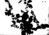
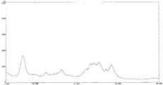
チタニルフタロシアニン結晶の粒子サイズをより細かくするために、本発明者らが観察したところによれば、前述の不定形チタニルフタロシアニン(低結晶性チタニルフタロシアニン)は、一次粒径が0.1μm以下(そのほとんどが0.01〜0.05μm程度)であるが(図1参照、なお図中のスケールバーは0.2μmを示す)、結晶変換に際しては、結晶成長と共に結晶変換されることが分かった。
通常、この種の結晶変換においては、原料の残存をおそれて充分な結晶変換時間を確保し、結晶変換が十二分に行なわれた後に、濾過を行ない、所望の結晶型を有するチタニルフタロシアニン結晶を得るものである。このため、原料として充分に小さな一次粒子を有する原料を用いているにもかかわらず、結晶変換後の結晶としては一次粒子の大きな結晶(概ね0.3〜0.5μm)が得られていた(図2参照、なお図中のスケールバーは0.2μmを示す)。There are two main methods for controlling the particle size of titanyl phthalocyanine crystals contained in the photosensitive layer. One is a method of synthesizing a crystal not containing particles larger than 0.25 μm when synthesizing titanyl phthalocyanine crystal particles, and the other is a coarse particle larger than 0.25 μm after the titanyl phthalocyanine crystal is dispersed. It is a method to remove. Of course, using both in combination has a greater effect.
First, a method for synthesizing fine-particle titanyl phthalocyanine crystals will be described.
In order to make the particle size of the titanyl phthalocyanine crystal finer, the present inventors have observed that the above-mentioned amorphous titanyl phthalocyanine (low crystalline titanyl phthalocyanine) has a primary particle size of 0.1 μm or less (its Although most of them are about 0.01 to 0.05 μm (see FIG. 1, the scale bar in the figure indicates 0.2 μm), it was found that during crystal conversion, crystal conversion is accompanied by crystal growth.
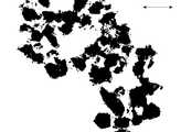
Usually, in this type of crystal conversion, a sufficient crystal conversion time is ensured due to fear of remaining of the raw material, and after the crystal conversion is sufficiently performed, filtration is performed to obtain a titanyl phthalocyanine crystal having a desired crystal type. Is what you get. For this reason, even though a raw material having sufficiently small primary particles is used as the raw material, a crystal having a large primary particle (approximately 0.3 to 0.5 μm) was obtained as the crystal after crystal conversion ( (See FIG. 2, where the scale bar indicates 0.2 μm).
このように作製されたチタニルフタロシアニン結晶を分散するにあたっては、分散後の粒子サイズを小さなもの(0.25μm以下、好ましくは0.20μm以下)にするため、強いシェアを与えて分散を行い、さらには必要に応じて一次粒子を粉砕する強いエネルギーを与えて分散を行なっている。この結果、前述の如き、粒子の一部が所望の結晶型でない結晶型へと転移してしまうことがあった。 In dispersing the titanyl phthalocyanine crystal prepared in this way, in order to make the particle size after dispersion small (0.25 μm or less, preferably 0.20 μm or less), dispersion is performed by giving a strong share. Distributes by applying strong energy to pulverize the primary particles as needed. As a result, as described above, some of the particles may be transferred to a crystal type that is not a desired crystal type.
一方、本発明においては、結晶変換に際して結晶成長がほとんど起こらない範囲(図1に観察される不定形チタニルフタロシアニン粒子のサイズが、結晶変換後において遜色ない小ささ、概ね0.2μm以下に保たれる範囲)で、結晶変換が完了した時点を見極めることによって、可能な限り一次粒子サイズの小さなチタニルフタロシアニン結晶を得ようというものである。
結晶変換後の粒子サイズは、結晶変換時間に比例して大きくなる。このため前述のように、結晶変換の効率を高くし、短時間で完了させることが重要である。このためには、いくつかの重要なポイントが挙げられる。On the other hand, in the present invention, the range in which crystal growth hardly occurs at the time of crystal conversion (the size of the amorphous titanyl phthalocyanine particles observed in FIG. 1 is kept in a small size, approximately 0.2 μm or less after crystal conversion. In other words, it is intended to obtain a titanyl phthalocyanine crystal having a primary particle size as small as possible by determining when the crystal conversion is completed.
The particle size after crystal conversion increases in proportion to the crystal conversion time. For this reason, as described above, it is important to increase the efficiency of crystal conversion and complete it in a short time. There are several important points for this.
1つは、結晶変換溶媒を前述のように適正なものを選択し、結晶変換効率を高めることである。
もう1つは、結晶変換を短時間に完了させるために、溶媒とチタニルフタロシアニン水ペースト(前述の如き作製した原料:不定形チタニルフタロシアニン)を充分に接触させるために強い撹拌を用いるものである。具体的には、撹拌力の非常に強いプロペラを用いた撹拌、ホモジナイザー(ホモミキサー)のような強烈な撹拌(分散)手段を用いるなどの手法によって、短時間での結晶変換を実現させるものである。
これらの条件によって、原料が残存することなく、結晶変換が充分に行なわれ、かつ結晶成長が起こらない状態のチタニルフタロシアニン結晶を得ることができる。この場合にも、結晶変換に使用する有機溶媒量の適正化が有効な手段である。具体的には、不定形チタニルフタロシアニンの固形分に対して、10倍以上、好ましくは30倍以上の有機溶媒を使用することが望ましい。これにより、短時間での結晶変換を確実なものとすると共に、不定形チタニルフタロシアニン中に含まれる不純物を確実に取り除くことができる。One is to select an appropriate crystal conversion solvent as described above to enhance the crystal conversion efficiency.
The other is to use strong stirring to bring the solvent into contact with the titanyl phthalocyanine aqueous paste (raw material prepared as described above: amorphous titanyl phthalocyanine) in order to complete the crystal conversion in a short time. Specifically, it is possible to realize crystal transformation in a short time by using a method such as stirring using a propeller with a very strong stirring force or using a strong stirring (dispersing) means such as a homogenizer (homomixer). is there.
Under these conditions, it is possible to obtain a titanyl phthalocyanine crystal in a state in which crystal conversion is sufficiently performed and crystal growth does not occur without remaining raw materials. Also in this case, optimization of the amount of organic solvent used for crystal conversion is an effective means. Specifically, it is desirable to use 10 times or more, preferably 30 times or more of the organic solvent with respect to the solid content of the amorphous titanyl phthalocyanine. Thereby, crystal conversion in a short time can be ensured and impurities contained in the amorphous titanyl phthalocyanine can be surely removed.
また、上述のように結晶粒子サイズと結晶変換時間は比例関係にあるため、所定の反応(結晶変換)が完了したら、反応を直ちに停止させる方法も有効な手段である。
上述のように結晶変換を行なった後、直ちに結晶変換の起こりにくい溶媒を大量に添加することが前記手段として挙げられる。結晶変換の起こりにくい溶媒としては、アルコール系、エステル系などの溶媒が挙げられる。これらの溶媒を結晶変換溶媒に対して、10倍程度加えることにより、結晶変換を停止することができる。In addition, since the crystal grain size and the crystal conversion time are in a proportional relationship as described above, a method of immediately stopping the reaction when a predetermined reaction (crystal conversion) is completed is also an effective means.
As the above-mentioned means, it is possible to immediately add a large amount of a solvent in which crystal conversion hardly occurs after crystal conversion as described above. Examples of the solvent that hardly causes crystal transformation include alcohol solvents and ester solvents. Crystal conversion can be stopped by adding about 10 times these solvents to the crystal conversion solvent.
このようにして作製される結晶は、一次粒径がより小さく、地汚れの抑制に有利となるが、顔料作製にかかる次工程(顔料の濾過工程)、分散液での分散安定性を考慮すると、あまり小さすぎても副作用が出る場合がある。
即ち、一次粒子が非常に細かい場合には、これを濾過する工程において濾過時間が非常に長くなってしまうという問題が発生する。また、一次粒子が小さすぎる場合には、分散液中での顔料粒子の表面積が大きくなるため、粒子の再凝集の可能性が高くなり、逆に地汚れの発生を促進させる恐れが出てくる。
したがって、適切な顔料粒子の粒子サイズは、およそ0.05μm〜0.2μm程度の範囲である。The crystals produced in this way have a smaller primary particle size, which is advantageous for suppressing background stains. However, when considering the next step for pigment preparation (pigment filtration step) and the dispersion stability in the dispersion liquid. If it is too small, there may be side effects.
That is, when the primary particles are very fine, there arises a problem that the filtration time becomes very long in the step of filtering the primary particles. In addition, if the primary particles are too small, the surface area of the pigment particles in the dispersion increases, so the possibility of reaggregation of the particles increases, and conversely, the occurrence of soiling may be promoted. .
Therefore, the suitable particle size of the pigment particles is in the range of about 0.05 μm to 0.2 μm.
図3には、短時間で結晶変換を行なった場合のチタニルフタロシアニン結晶のTEM像を示す。なお、図中のスケールバーは0.2μmを示す。図2の場合とは異なり、粒子サイズが小さく、ほぼ均一であり、図2に観察されるような粗大粒子は全く認められない。 FIG. 3 shows a TEM image of a titanyl phthalocyanine crystal when crystal conversion is performed in a short time. In addition, the scale bar in a figure shows 0.2 micrometer. Unlike the case of FIG. 2, the particle size is small and almost uniform, and no coarse particles as observed in FIG. 2 are observed.
このように作製されたチタニルフタロシアニン結晶を分散するにあたっては、合成後のチタニルフタロシアニンの一次粒子は充分に小さいため、図2に示すような粗大粒子を含むチタニルフタロシアニンを分散する際に必要となる強いシェアを与えずとも、所望の平均粒子サイズ(0.25μm以下、好ましくは0.2μm以下)を得ることが可能となる。この結果、過度の分散によって粒子の一部が所望の結晶型とは異なる結晶型に転移してしまう不具合を抑制することが可能となる。 In dispersing the titanyl phthalocyanine crystal prepared in this way, the primary particles of the titanyl phthalocyanine after synthesis are sufficiently small, so that it is necessary to disperse the titanyl phthalocyanine containing coarse particles as shown in FIG. A desired average particle size (0.25 μm or less, preferably 0.2 μm or less) can be obtained without giving a share. As a result, it is possible to suppress a problem that a part of the particles are transferred to a crystal type different from the desired crystal type due to excessive dispersion.
ここでいう平均粒子サイズとは、体積平均粒径として、超遠心式自動粒度分布測定装置:CAPA−700(堀場製作所製)により求めたものであり、この際、累積分布の50%に相当する粒子径(Median系)として算出されたものである。
しかしながら、この方法では微量の粗大粒子を検出できない場合があるため、より詳細に求めるには、チタニルフタロシアニン結晶粉末、あるいは分散液を直接、電子顕微鏡にて観察し、その大きさを求めることが重要である。The average particle size referred to here is a volume average particle size obtained by an ultracentrifugal automatic particle size distribution analyzer: CAPA-700 (manufactured by Horiba Seisakusho), which corresponds to 50% of the cumulative distribution. It is calculated as a particle size (Median system).
However, this method may not be able to detect a very small amount of coarse particles. Therefore, in order to obtain more details, it is important to observe the titanyl phthalocyanine crystal powder or dispersion directly with an electron microscope and determine its size. It is.
分散液をさらに観察して微小欠陥について検討した結果、上記現象は次のように説明される。
通常、平均粒子サイズを測定する方法において、極端に大きな粒子が数%以上も存在するような場合には、その存在が検出できるが、全体の1%以下程度のような微量になってくると、その測定は検出限界以下になってしまう。その結果、平均粒子サイズの測定だけでは粗大粒子の存在が検出されずに、上述のような微小欠陥に関する解釈を困難にしていた。As a result of further observing the dispersion liquid and examining minute defects, the above phenomenon is explained as follows.
Usually, in the method of measuring the average particle size, when extremely large particles are present in a few percent or more, the presence can be detected, but when the amount becomes as small as about 1% or less of the whole. The measurement is below the detection limit. As a result, the presence of coarse particles is not detected only by measuring the average particle size, making it difficult to interpret the minute defects as described above.
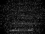
図4及び図5に、分散条件を固定して分散時間だけを変更した2種類の分散液の状態を観察した写真を示す。
同一条件における分散時間の短い分散液の写真を図4に示すが、分散時間の長い図5と比較して、図4中の黒い粒として観察される粗大粒子が多く残っている様子が観測される。
この2種類の分散液の平均粒径並びに粒度分布を公知の方法に従って、市販の粒度分布測定装置(堀場製作所製:超遠心式自動粒度分布測定装置、CAPA700)によって測定した。その結果を図6に示す。
図6における「A」が図4に示す分散液に対応し、「B」が図5に示す分散液に対応する。両者を比較すると、粒度分布に関してはほとんど差が認められない。また、両者の平均粒径値は、「A」が0.29μm、「B」が0.28μmと求められ、測定誤差を加味した上では、両者に明らかな差があるとは判断できない。4 and 5 show photographs observing the states of two types of dispersions in which only the dispersion time is changed while fixing the dispersion conditions.
A photograph of a dispersion liquid with a short dispersion time under the same conditions is shown in FIG. 4. Compared with FIG. 5 with a long dispersion time, a large number of coarse particles observed as black particles in FIG. 4 remain. The
The average particle size and particle size distribution of these two types of dispersions were measured by a commercially available particle size distribution measuring device (manufactured by Horiba: ultracentrifugal automatic particle size distribution measuring device, CAPA700). The result is shown in FIG.
“A” in FIG. 6 corresponds to the dispersion shown in FIG. 4, and “B” corresponds to the dispersion shown in FIG. When both are compared, there is almost no difference in the particle size distribution. In addition, the average particle diameter values of both are obtained as “A” of 0.29 μm and “B” of 0.28 μm, and it cannot be determined that there is a clear difference between them, taking measurement errors into account.
したがって、公知の平均粒径(粒子サイズ)の規定だけでは、微量な粗大粒子の残存量を検出することはできず、地肌汚れとの関係を明確にすることは難しい。この微量な粗大粒子の存在は、塗工液を顕微鏡等で観察することにより、初めて認識されるものであり、これによって地肌汚れとの関係を明らかにすることが可能となった。 Therefore, it is difficult to detect the residual amount of a very small amount of coarse particles only by defining a known average particle size (particle size), and it is difficult to clarify the relationship with background dirt. The presence of this minute amount of coarse particles is recognized for the first time by observing the coating liquid with a microscope or the like, and this makes it possible to clarify the relationship with the background dirt.
このような結果から、凝集を抑制しつつ、結晶変換時に作製される一次粒子をできる限り小さくするために、結晶変換溶媒を前述のように適正なものを選択し、結晶変換効率を高めつつ、結晶変換を短時間に完了させるために、溶媒とチタニルフタロシアニン水ペースト(前述の如き作製した原料)を充分に接触させるために強い撹拌を用いるような手法は有効であることがわかる。 From these results, in order to make the primary particles produced during crystal conversion as small as possible while suppressing aggregation, an appropriate crystal conversion solvent is selected as described above, while increasing the crystal conversion efficiency, In order to complete the crystal conversion in a short time, it can be seen that a technique using strong stirring is effective for sufficiently bringing the solvent into contact with the titanyl phthalocyanine aqueous paste (the raw material prepared as described above).
このような結晶変換方法を採用することにより、一次粒子サイズの小さな(0.25μm以下、好ましくは0.2μm以下)チタニルフタロシアニン結晶を得ることができる。前記特許文献1に記載された技術に加えて、必要に応じて上述のような技術(微細なチタニルフタロシアニン結晶を得るための結晶変換方法)を併用することは、本発明の効果を高めるために有効な手段である。 By employing such a crystal conversion method, a titanyl phthalocyanine crystal having a small primary particle size (0.25 μm or less, preferably 0.2 μm or less) can be obtained. In order to enhance the effect of the present invention, in combination with the technique described in
続いて、結晶変換されたチタニルフタロシアニン結晶は直ちに濾過されることにより、結晶変換溶媒と分別される。この濾過に際しては、適当なサイズのフィルターを用いることにより行なわれる。この際、減圧濾過を用いることが最も適当である。
その後、分別されたチタニルフタロシアニン結晶は、必要に応じて加熱乾燥される。加熱乾燥に使用する乾燥機は、公知のものがいずれも使用可能であるが、大気下で行なう場合には送風型の乾燥機が好ましい。更に、乾燥速度を早め、本発明の効果をより顕著に発現させるために減圧下の乾燥も非常に有効な手段である。特に、高温で分解する、あるいは結晶型が変化するような材料に対しては有効な手段である。特に10mmHgよりも真空度が高い状態で乾燥することが有効である。Subsequently, the crystallized titanyl phthalocyanine crystal is immediately filtered to be separated from the crystal conversion solvent. This filtration is performed by using a filter of an appropriate size. In this case, it is most appropriate to use vacuum filtration.
Thereafter, the separated titanyl phthalocyanine crystal is heat-dried as necessary. Any known dryer can be used for heating and drying, but a blower-type dryer is preferable when the drying is performed in the atmosphere. Furthermore, drying under reduced pressure is also a very effective means in order to increase the drying speed and to exhibit the effects of the present invention more remarkably. In particular, this is an effective means for a material that decomposes at a high temperature or changes its crystal form. It is particularly effective to dry in a state where the degree of vacuum is higher than 10 mmHg.
このように得られた特定の結晶型を有するチタニルフタロシアニン結晶は、電子写真感光体用電荷発生物質として極めて有用である。しかしながら、先述のように結晶型が不安定であり、分散液を作製する際に結晶型が転移し易いという欠点を有していた。 しかしながら、本発明のように一次粒子を限りなく小さくした結晶を合成することによって、分散液作製時に過剰なシェアを与えることなく、平均粒径の小さな分散液を作製することができ、結晶型も極めて安定に(合成した結晶型を変えることなく)作製することが可能となる。 The thus obtained titanyl phthalocyanine crystal having a specific crystal type is extremely useful as a charge generating material for an electrophotographic photoreceptor. However, as described above, the crystal type is unstable, and the crystal type is easily transferred when a dispersion is prepared. However, by synthesizing crystals with primary particles as small as possible as in the present invention, it is possible to produce a dispersion with a small average particle size without giving an excessive share during the preparation of the dispersion. It becomes possible to produce it very stably (without changing the synthesized crystal form).
分散液の作製に関しては一般的な方法が用いられ、前記チタニルフタロシアニン結晶を必要に応じてバインダー樹脂とともに適当な溶剤中にボールミル、アトライター、サンドミル、ビーズミル、超音波などを用いて分散することで得られるものである。
この際、バインダー樹脂は感光体の静電特性などにより、また溶媒は顔料へのぬれ性、顔料の分散性などによって選択すればよい。A general method is used for the preparation of the dispersion, and the titanyl phthalocyanine crystal is dispersed in a suitable solvent together with a binder resin as necessary by using a ball mill, an attritor, a sand mill, a bead mill, an ultrasonic wave, or the like. It is obtained.
At this time, the binder resin may be selected depending on the electrostatic characteristics of the photoreceptor, and the solvent may be selected depending on the wettability to the pigment, the dispersibility of the pigment, and the like.
既に述べたように、CuKα線(波長1.542Å)に対するブラッグ角2θの回折ピーク(±0.2゜)として、少なくとも27.2゜に最大回折ピークを有するチタニルフタロシアニン結晶は、熱エネルギー・機械的シェア等のストレスにより他の結晶型に容易に結晶転移をすることが知られている。本発明で用いるチタニルフタロシアニン結晶もこの傾向は変わらない。
すなわち、微細な粒子を含む分散液を作製するためには、分散方法の工夫も必要であるが、結晶型の安定性と微粒子化はトレード・オフの関係になりがちである。分散条件を最適化することによってこれを回避する方法はあるが、いずれも製造条件を極めて狭くしてしまうものであり、より簡便な方法が望まれている。この問題を解決するために、以下のような方法も有効な手段である。As already mentioned, the titanyl phthalocyanine crystal having a maximum diffraction peak at 27.2 ° as a diffraction peak (± 0.2 °) with a Bragg angle 2θ with respect to CuKα rays (wavelength 1.542 mm) is It is known that a crystal transition easily occurs to another crystal type due to a stress such as a dynamic share. This tendency does not change in the titanyl phthalocyanine crystal used in the present invention.
In other words, in order to produce a dispersion containing fine particles, it is necessary to devise a dispersion method, but the stability of the crystal form and the micronization tend to be in a trade-off relationship. Although there are methods for avoiding this by optimizing the dispersion conditions, all of them make the manufacturing conditions extremely narrow, and a simpler method is desired. In order to solve this problem, the following method is also an effective means.
すなわち、結晶転移が起こらない範囲でできる限り粒子を微細にした分散液を作製後、適当なフィルターで濾過を行ない、粗大粒子を取り除く方法である。この方法では、残存する目視では観察できない(あるいは粒径測定では検出できない)微量な粗大粒子をも取り除くことができ、また粒度分布を揃えるという点からも非常に有効な手段である。
具体的には、上述のように作製した分散液を、有効孔径が3μm以下のフィルター、より好ましくは1μm以下のフィルターにて濾過する操作を行ない、分散液を完成させるというものである。
この方法によっても、粒子サイズの小さな(0.25μm以下、好ましくは0.2μm以下)チタニルフタロシアニン結晶のみを含む分散液を作製することができ、これを用いて作製した感光体を画像形成装置に搭載することによって、地汚れに対する余裕度を高めることが可能となり、感光体の高耐久化に対し有効となる。
この際、濾過される分散液の粒子サイズが大きすぎたり、粒度分布が広すぎたりする場合には、濾過によるロスが大きくなったり、濾過の目詰まりを生じて濾過が不可能になったりする場合がある。このため、濾過前の分散液においては、平均粒子サイズが0.3μm以下で、その標準偏差が0.2μm以下に到達するまで分散を行った方が望ましい。平均粒子サイズが0.3μm以上である場合には濾過によるロスが大きくなり、標準偏差が0.2μm以上である場合には濾過時間が非常に長くなったりする不具合が生じる場合がある。That is, after preparing a dispersion liquid in which particles are made as fine as possible within a range where crystal transition does not occur, filtration is performed with an appropriate filter to remove coarse particles. This method is a very effective means in that it can remove a minute amount of coarse particles that cannot be visually observed (or cannot be detected by particle size measurement), and that the particle size distribution is uniform.
Specifically, the dispersion prepared as described above is filtered through a filter having an effective pore size of 3 μm or less, more preferably 1 μm or less, thereby completing the dispersion.
Also by this method, a dispersion liquid containing only titanyl phthalocyanine crystals having a small particle size (0.25 μm or less, preferably 0.2 μm or less) can be produced, and a photoreceptor produced using the dispersion is used as an image forming apparatus. By mounting, it is possible to increase the margin against soiling, which is effective for improving the durability of the photoreceptor.
At this time, when the particle size of the dispersion to be filtered is too large or the particle size distribution is too wide, the loss due to filtration becomes large or the filtration becomes clogged and filtration becomes impossible. There is a case. For this reason, in the dispersion before filtration, it is desirable to carry out dispersion until the average particle size is 0.3 μm or less and the standard deviation reaches 0.2 μm or less. When the average particle size is 0.3 μm or more, the loss due to filtration increases, and when the standard deviation is 0.2 μm or more, there may be a problem that the filtration time becomes very long.
分散液を濾過するフィルターに関しては、除去したい粗大粒子のサイズによって異なるものであるが、本発明者等の検討によれば、600dpi程度の解像度を必要とする画像形成装置で使用される感光体としては、最低でも3μm以上の粗大粒子の存在は画像に対して影響を及ぼす。
したがって、有効孔径が3μm以下のフィルターを使用すべきである。より好ましくは1μm以下の有効孔径を有するフィルターを使用することである。
この有効孔径に関しては、細かいほど粗大粒子の除去に効果があるものであるが、あまり細かすぎると、必要な顔料粒子そのものも濾過されてしまったり、また、濾過に時間がかかる、フィルターが目詰まりを起こす、ポンプ等を使用して送液する場合には負荷がかかりすぎる等の問題を生じるため、適切な有効孔径を有するフィルターを選択する必要がある。
なお、ここで使用されるフィルターの材質は、当然のことながら濾過する分散液に使用される溶媒に対して耐性のあるものが使用される。The filter for filtering the dispersion varies depending on the size of coarse particles to be removed, but according to the study by the present inventors, as a photoreceptor used in an image forming apparatus that requires a resolution of about 600 dpi. The presence of coarse particles of at least 3 μm affects the image.
Therefore, a filter with an effective pore size of 3 μm or less should be used. More preferably, a filter having an effective pore size of 1 μm or less is used.
As for the effective pore size, the finer the particle, the more effective it is for removing coarse particles. In the case of liquid feeding using a pump or the like, there is a problem that the load is excessively applied. Therefore, it is necessary to select a filter having an appropriate effective pore size.
As a matter of course, a material having resistance to the solvent used in the dispersion to be filtered is used as the material of the filter used here.
このような分散液の濾過操作を加えることによっても、粗大粒子を取り除くことが可能になり、ひいては分散液を使用した感光体で発生する地汚れを低減化することができる。
上述のように、より細かいフィルターを使用するほど、その効果は大きなもの(確実なもの)になるが、場合によっては顔料粒子そのものが濾過されてしまう不具合が生じる恐れがある。
このような場合には、先に述べた一次粒子を微細化したチタニルフタロシアニンの合成技術と併用することによって、それらの不具合を解消することが可能となり、得られる効果は非常に大きくなる。By adding such an operation of filtering the dispersion, coarse particles can be removed, and as a result, background contamination generated on the photoconductor using the dispersion can be reduced.
As described above, the finer the filter, the greater the effect (reliable), but there is a possibility that the pigment particles themselves may be filtered in some cases.
In such a case, by using the primary particles described above in combination with the refined titanyl phthalocyanine synthesis technique, it is possible to eliminate these problems, and the obtained effect becomes very large.
即ち、(1)微細化チタニルフタロシアニンを合成し、これを使用することにより、分散時間の短縮化・分散ストレスの低減化が図れ、分散における結晶転移の可能性が小さくなる。(2)分散によって残存する粗大粒子サイズが、微細化しない場合よりも小さいため、より小さなフィルターを使用することが可能になり、粗大粒子の除去効果がより確実なものとなる。また、除去されるチタニルフタロシアニン粒子量が低減し、濾過前後における分散液組成の変化が少なく、安定した製造が可能になる。(3)その結果、製造される感光体は安定して地汚れ耐性の高い電子写真感光体が製造されることになる。 That is, (1) by synthesizing and using refined titanyl phthalocyanine, the dispersion time can be shortened and the dispersion stress can be reduced, and the possibility of crystal transition in dispersion is reduced. (2) Since the size of coarse particles remaining by dispersion is smaller than that in the case where the particles are not refined, a smaller filter can be used, and the effect of removing coarse particles becomes more reliable. In addition, the amount of titanyl phthalocyanine particles to be removed is reduced, and there is little change in the composition of the dispersion before and after filtration, which enables stable production. (3) As a result, an electrophotographic photosensitive member having a stable background stain resistance is stably produced.
次に、本発明の電子写真感光体における構成要素の1つの架橋型電荷輸送層について説明する。
架橋型電荷輸送層は、電子写真感光体の繰り返し使用によって起こる摩耗の影響を軽減し、電界強度の増加によって増加する地汚れの経時安定性を高め、さらに静電安定性や画質安定性を高めることによって経時安定性と耐久性を両立させることを目的として形成されるものである。
電子写真感光体表面に形成される傷や表面に付着する異物(トナー、トナーの外添剤、キャリア、紙粉等)は、電子写真感光体のクリーニング性を低下させ、画質安定性を顕著に低下させる。
したがって、電子写真感光体の高耐久化を実現させるためには、耐摩耗性を高めるだけでなく、電子写真感光体表面の傷やフィルミングの影響を最小限にすることが重要であり、そのためには高硬度、高弾性でかつ平滑な表面層を形成させることが好ましい。Next, one cross-linked charge transport layer as a constituent element in the electrophotographic photoreceptor of the present invention will be described.
The cross-linked charge transport layer reduces the effects of wear caused by repeated use of the electrophotographic photosensitive member, increases the aging stability of the soil that increases due to an increase in the electric field strength, and further increases the electrostatic stability and image quality stability. Thus, it is formed for the purpose of achieving both stability over time and durability.
Scratches formed on the surface of the electrophotographic photosensitive member and foreign substances adhering to the surface (toner, toner external additives, carrier, paper dust, etc.) reduce the cleaning property of the electrophotographic photosensitive member and significantly improve the image quality stability. Reduce.
Therefore, in order to achieve high durability of the electrophotographic photosensitive member, it is important not only to increase the wear resistance but also to minimize the influence of scratches and filming on the surface of the electrophotographic photosensitive member. It is preferable to form a smooth surface layer with high hardness, high elasticity and smoothness.
本発明の電子写真感光体の表面層を形成する架橋型電荷輸送層は、3官能以上のラジカル重合性モノマーを硬化した架橋構造を有するため3次元の網目構造が発達し、架橋密度が非常に高い高硬度且つ高弾性な表面層が得られ、かつ均一で平滑性も高く、高い耐摩耗性、耐傷性が達成される。
このように電子写真感光体の表面の架橋密度すなわち単位体積あたりの架橋結合数を増加させることが重要であるが、硬化反応において瞬時に多数の結合を形成させるため体積収縮による内部応力が発生する。この内部応力は、架橋型電荷輸送層の膜厚が厚くなるほど増加するため電荷輸送層全層を硬化させると、クラックや膜剥がれが発生しやすくなる。
この現象は、初期的に現れなくても、電子写真プロセス上で繰り返し使用され帯電、現像、転写、クリーニングのハザード及び熱変動の影響を受けることにより、経時で発生しやすくなることもある。The cross-linked charge transport layer forming the surface layer of the electrophotographic photoreceptor of the present invention has a cross-linked structure obtained by curing a tri- or higher functional radical polymerizable monomer, so that a three-dimensional network structure is developed and the cross-linking density is very high. A high hardness and high elasticity surface layer can be obtained, and the surface layer is uniform and smooth, and high wear resistance and scratch resistance are achieved.
As described above, it is important to increase the crosslink density on the surface of the electrophotographic photosensitive member, that is, the number of crosslink bonds per unit volume. However, since a large number of bonds are instantaneously formed in the curing reaction, internal stress due to volume shrinkage occurs. . Since this internal stress increases as the film thickness of the crosslinkable charge transport layer increases, cracks and film peeling tend to occur when the entire charge transport layer is cured.
Even if this phenomenon does not appear initially, it may be likely to occur over time due to repeated use in the electrophotographic process and the effects of charging, development, transfer, cleaning hazards and thermal fluctuations.
この問題を解決する方法としては、(1)架橋層及び架橋構造に高分子成分を導入する、(2)1官能及び2官能のラジカル重合性モノマーを多量に用いる、(3)柔軟性基を有する多官能モノマーを用いる、などの硬化樹脂層を柔らかくする方向性が挙げられるが、いずれも架橋層の架橋密度が希薄となり、飛躍的な耐摩耗性が達成されないことを確認した。
これに対し、本発明の電子写真感光体においては、電荷輸送層上に3次元の網目構造が発達した架橋密度の高い架橋型電荷輸送層が1μm以上、10μm以下の膜厚で設けたものとすることによって、上記のクラックや膜剥がれを発生させず、且つ非常に高い耐摩耗性を達成することができたものである。
かかる架橋型電荷輸送層の膜厚を2μm以上、8μm以下の膜厚にすることによって、さらに上記問題に対する余裕度が向上することに加え、更なる耐摩耗性向上に繋がる高架橋密度化の材料選択が可能となる。As a method for solving this problem, (1) a polymer component is introduced into the crosslinked layer and the crosslinked structure, (2) a large amount of monofunctional and bifunctional radically polymerizable monomers are used, and (3) a flexible group is introduced. Although the directionality which softens the cured resin layer, such as using the polyfunctional monomer which has is mentioned, the crosslink density of the crosslinked layer became thin, and it was confirmed that dramatic wear resistance was not achieved.
On the other hand, in the electrophotographic photosensitive member of the present invention, a cross-linked charge transport layer having a high cross-linking density and having a three-dimensional network structure formed on the charge transport layer is provided with a film thickness of 1 μm or more and 10 μm or less. By doing so, the above-described cracks and film peeling did not occur, and very high wear resistance could be achieved.
By selecting a film thickness of the crosslinkable charge transport layer of 2 μm or more and 8 μm or less, in addition to further improving the margin for the above problem, a material selection for increasing the crosslink density that leads to further improvement of wear resistance. Is possible.
本発明の電子写真感光体がクラックや膜剥がれを抑制できる理由としては、架橋型電荷輸送層を薄膜化できるため内部応力が大きくならないこと、下層に電荷輸送層を有するため表面の架橋型電荷輸送層の内部応力を緩和できることなどによるものと考えられる。
このために、架橋型電荷輸送層に高分子材料を多量に含有させる必要がなく、この時生ずる、高分子材料とラジカル重合性組成物(ラジカル重合性モノマーや電荷輸送性構造を有するラジカル重合性化合物)の反応によって生じた硬化物との不相溶が原因で発生する傷やトナーフィルミングも起こりにくい。
さらに、電荷輸送層全層にわたる厚膜を光エネルギー照射によって硬化する場合、電荷輸送性構造による吸収から内部への光透過が制限され、硬化反応が充分に進行しない現象が起こることがある。
本発明の電子写真感光体の架橋型電荷輸送層が、10μm以下の薄膜であるために、内部まで均一に硬化反応が進行し、表面と同様に内部でも高い耐摩耗性が維持される。
また、本発明における該架橋型電荷輸送層の形成においては、上記3官能性ラジカル重合性モノマーに加え、さらに1官能の電荷輸送性構造を有するラジカル重合性化合物を含有させており、これが上記3官能以上のラジカル重合性モノマー硬化時に架橋結合中に取り込まれる。
これに対し、官能基を有しない低分子電荷輸送物質を架橋表面層中に含有させた場合には、その相溶性の低さから低分子電荷輸送物質の析出や白濁現象が起こり、架橋表面層の機械的強度も低下する。
一方、2官能以上の電荷輸送性化合物を主成分として用いた場合には、複数の結合で架橋構造中に固定され架橋密度はより高まるが、電荷輸送性構造が非常に嵩高いため硬化樹脂構造の歪みが非常に大きくなり、架橋型電荷輸送層の内部応力が高まる原因となる。The reason why the electrophotographic photoreceptor of the present invention can suppress cracks and film peeling is that the cross-linked charge transport layer can be made thin, so that the internal stress does not increase, and since the charge transport layer is provided in the lower layer, the cross-linked charge transport on the surface This is thought to be due to the ability to relieve the internal stress of the layer.
For this reason, it is not necessary to contain a large amount of the polymer material in the cross-linkable charge transport layer, and the polymer material and the radical polymerizable composition (radical polymerizable monomer or radical polymerizable compound having a charge transport structure) generated at this time. Scratches and toner filming caused by incompatibility with the cured product caused by the reaction of the compound) are also difficult to occur.
Further, when a thick film over the entire charge transport layer is cured by light energy irradiation, light transmission from the absorption by the charge transport structure to the inside is limited, and a phenomenon in which the curing reaction does not proceed sufficiently may occur.
Since the crosslinkable charge transport layer of the electrophotographic photoreceptor of the present invention is a thin film having a thickness of 10 μm or less, the curing reaction proceeds uniformly to the inside, and high wear resistance is maintained inside as well as the surface.
In addition, in the formation of the crosslinkable charge transport layer in the present invention, in addition to the trifunctional radical polymerizable monomer, a radical polymerizable compound having a monofunctional charge transporting structure is further contained. Incorporated into the cross-linking during curing of the radical polymerizable monomer higher than the functional group.
On the other hand, when a low molecular charge transport material having no functional group is contained in the cross-linked surface layer, precipitation of low molecular charge transport material and white turbidity occur due to its low compatibility. The mechanical strength of the steel also decreases.
On the other hand, when a bifunctional or higher functional charge transporting compound is used as a main component, a plurality of bonds are fixed in the cross-linking structure and the cross-linking density is further increased, but the charge transporting structure is very bulky, so the cured resin structure Becomes very large, which increases the internal stress of the cross-linked charge transport layer.
さらに、本発明の電子写真感光体は、良好な電気的特性を有し、このため繰り返し安定性に優れており、高耐久化並びに高安定化が実現される。
これは、架橋型電荷輸送層の構成材料として1官能の電荷輸送性構造を有するラジカル重合性化合物を用い、架橋結合間にペンダント状に固定化したことに起因するためである。
上記のように、官能基を有しない電荷輸送物質の場合には、析出、白濁現象が起こり、感度の低下、残留電位の上昇等繰り返し使用における電気的特性の劣化が著しい。2官能以上の電荷輸送性化合物を主成分として用いた場合には、複数の結合で架橋構造中に固定されるため、電荷輸送時の中間体構造(カチオンラジカル)が安定して保てず、電荷のトラップによる感度の低下、残留電位の上昇が起こりやすい。
これらの電気的特性の劣化は、画像濃度低下、文字細り等の画像として現れる。さらに、本発明の電子写真感光体においては、下層の電荷輸送層として従来感光体の電荷トラップの少ない高移動度な設計が適応可能で、架橋型電荷輸送層の電気的副作用を最小限に抑えることができる。Furthermore, the electrophotographic photosensitive member of the present invention has good electrical characteristics, and is therefore excellent in repetitive stability, realizing high durability and high stability.
This is because a radical polymerizable compound having a monofunctional charge transporting structure is used as a constituent material of the crosslinkable charge transporting layer and is immobilized in a pendant shape between the crosslinks.
As described above, in the case of a charge transport material having no functional group, precipitation and turbidity occur, and the deterioration of electrical characteristics due to repeated use such as a decrease in sensitivity and an increase in residual potential is remarkable. When a bifunctional or higher functional charge transporting compound is used as the main component, the intermediate structure (cation radical) at the time of charge transport cannot be stably maintained because it is fixed in the crosslinked structure by a plurality of bonds. Sensitivity is decreased due to charge trapping, and residual potential is likely to increase.
Such deterioration of the electric characteristics appears as an image such as a decrease in image density and thinning of characters. Furthermore, in the electrophotographic photosensitive member of the present invention, a high mobility design with few charge traps of a conventional photosensitive member can be applied as a lower charge transport layer, and the electrical side effects of the cross-linked charge transport layer are minimized. be able to.
また、本発明における上記架橋型電荷輸送層形成において、架橋型電荷輸送層が有機溶剤に対し不溶性にすることによって、特にその飛躍的な耐摩耗性が発揮される。
該架橋型電荷輸送層は、電荷輸送性構造を有しない3官能以上のラジカル重合性モノマーと1官能の電荷輸送性構造を有するラジカル重合性化合物を硬化することにより形成され、層全体としては3次元の網目構造が発達し高い架橋密度を有するが、上記成分以外の含有物(例えば、1または2官能モノマー、高分子バインダー、酸化防止剤、レベリング剤、可塑剤などの添加剤及び下層からの溶解混入成分)や硬化条件により、局部的に架橋密度が希薄になったり、高密度に架橋した微小な硬化物の集合体として形成されることがある。
このような架橋型電荷輸送層は、硬化物間の結合力は弱く有機溶剤に対し溶解性を示し、且つ電子写真プロセス中で繰り返し使用されるなかで、局部的な摩耗や微小な硬化物単位での脱離が発生しやすくなる。
本発明のように架橋型電荷輸送層を有機溶剤に対し不溶性にせしめることによって、本来の3次元の網目構造が発達し高い架橋度を有することに加え、連鎖反応が広い範囲で進行し硬化物が高分子量化するため、飛躍的な耐摩耗性の向上が達成される。Further, in the formation of the crosslinkable charge transport layer in the present invention, particularly rapid wear resistance is exhibited by making the crosslinkable charge transport layer insoluble in the organic solvent.
The cross-linked charge transport layer is formed by curing a tri- or more functional radical polymerizable monomer having no charge transport structure and a radical polymerizable compound having a monofunctional charge transport structure. Dimensional network structure develops and has a high crosslinking density, but contains other than the above components (for example, mono- or bifunctional monomers, polymer binders, antioxidants, leveling agents, plasticizers and other additives and lower layers) Depending on the dissolved components) and curing conditions, the cross-linking density may be locally dilute or may be formed as an aggregate of minute cured products cross-linked at high density.
Such a crosslinkable charge transport layer has a weak bonding force between cured products and is soluble in an organic solvent, and is repeatedly used in an electrophotographic process. Elimination is likely to occur.
By making the cross-linkable charge transport layer insoluble in an organic solvent as in the present invention, the original three-dimensional network structure is developed and has a high degree of cross-linking, and the chain reaction proceeds in a wide range to obtain a cured product. Since the polymer has a high molecular weight, a dramatic improvement in wear resistance is achieved.
次に、本発明の架橋型電荷輸送層塗布液の構成材料について説明する。
本発明に用いられる電荷輸送性を有しない3官能以上のラジカル重合性モノマーとは、例えばトリアリールアミン、ヒドラゾン、ピラゾリン、カルバゾールなどの正孔輸送性構造、例えば縮合多環キノン、ジフェノキノン、シアノ基やニトロ基を有する電子吸引性芳香族環などの電子輸送構造を有しておらず、且つラジカル重合性官能基を3個以上有するモノマーを指す。
このラジカル重合性官能基とは、炭素−炭素2重結合を有するものであり、ラジカル重合可能な基であれば何れでもよい。これらラジカル重合性官能基としては、例えば、下記に示す1−置換エチレン官能基、1,1−置換エチレン官能基等が挙げられる。
(1)1−置換エチレン官能基としては、例えば以下の式で表される官能基が挙げられる。Next, the constituent materials of the crosslinking type charge transport layer coating solution of the present invention will be described.
The trifunctional or higher functional radical polymerizable monomer having no charge transporting property used in the present invention is a hole transporting structure such as triarylamine, hydrazone, pyrazoline, carbazole, such as condensed polycyclic quinone, diphenoquinone, cyano group. And a monomer having no electron transport structure such as an electron-withdrawing aromatic ring having a nitro group and having three or more radical polymerizable functional groups.
The radical polymerizable functional group has a carbon-carbon double bond and may be any radical polymerizable group. Examples of these radical polymerizable functional groups include 1-substituted ethylene functional groups and 1,1-substituted ethylene functional groups shown below.
(1) Examples of the 1-substituted ethylene functional group include functional groups represented by the following formulas.
これらの置換基を具体的に例示すると、ビニル基、スチリル基、2−メチル−1,3−ブタジエニル基、ビニルカルボニル基、アクリロイルオキシ基、アクリロイルアミド基、ビニルチオエーテル基等が挙げられる。
(2)1,1−置換エチレン官能基としては、例えば以下の式で表される官能基が挙げられる。
Specific examples of these substituents include a vinyl group, a styryl group, a 2-methyl-1,3-butadienyl group, a vinylcarbonyl group, an acryloyloxy group, an acryloylamide group, and a vinyl thioether group.
(2) Examples of the 1,1-substituted ethylene functional group include functional groups represented by the following formulas.
これらの置換基を具体的に例示すると、α−塩化アクリロイルオキシ基、メタクリロイルオキシ基、α−シアノエチレン基、α−シアノアクリロイルオキシ基、α−シアノフェニレン基、メタクリロイルアミノ基等が挙げられる。
なお、これらX、Yについての置換基にさらに置換される置換基としては、例えばハロゲン原子、ニトロ基、シアノ基、メチル基、エチル基等のアルキル基、メトキシ基、エトキシ基等のアルコキシ基、フェノキシ基等のアリールオキシ基、フェニル基、ナフチル基等のアリール基、ベンジル基、フェネチル基等のアラルキル基等が挙げられる。
これらのラジカル重合性官能基の中では、特にアクリロイルオキシ基、メタクリロイルオキシ基が有用であり、3個以上のアクリロイルオキシ基を有する化合物は、例えば水酸基がその分子中に3個以上ある化合物とアクリル酸(塩)、アクリル酸ハライド、アクリル酸エステルを用い、エステル反応あるいはエステル交換反応させることにより得ることができる。
また、3個以上のメタクリロイルオキシ基を有する化合物も同様にして得ることができる。また、ラジカル重合性官能基を3個以上有する単量体中のラジカル重合性官能基は、同一でも異なっても良い。Specific examples of these substituents include an α-acryloyloxy chloride group, a methacryloyloxy group, an α-cyanoethylene group, an α-cyanoacryloyloxy group, an α-cyanophenylene group, and a methacryloylamino group.
In addition, examples of the substituent further substituted with the substituent for X and Y include, for example, a halogen atom, a nitro group, an alkyl group such as a cyano group, a methyl group, and an ethyl group, an alkoxy group such as a methoxy group and an ethoxy group, Examples thereof include aryloxy groups such as phenoxy group, aryl groups such as phenyl group and naphthyl group, aralkyl groups such as benzyl group and phenethyl group.
Among these radical polymerizable functional groups, acryloyloxy group and methacryloyloxy group are particularly useful, and a compound having three or more acryloyloxy groups is, for example, a compound having three or more hydroxyl groups in the molecule and an acrylic group. It can be obtained by using an acid (salt), an acrylic acid halide, or an acrylic ester to cause an ester reaction or a transesterification reaction.
A compound having three or more methacryloyloxy groups can be obtained in the same manner. Further, the radical polymerizable functional groups in the monomer having three or more radical polymerizable functional groups may be the same or different.
電荷輸送性構造を有しない3官能以上の具体的なラジカル重合性モノマーとしては、以下のものが例示されるが、これらの化合物に限定されるものではない。
すなわち、本発明において使用する上記ラジカル重合性モノマーとしては、例えば、トリメチロールプロパントリアクリレート(TMPTA)、トリメチロールプロパントリメタクリレート、トリメチロールプロパンアルキレン変性トリアクリレート、トリメチロールプロパンエチレンオキシ変性(以後EO変性)トリアクリレート、トリメチロールプロパンプロピレンオキシ変性(以後PO変性)トリアクリレート、トリメチロールプロパンカプロラクトン変性トリアクリレート、トリメチロールプロパンアルキレン変性トリメタクリレート、ペンタエリスリトールトリアクリレート、ペンタエリスリトールテトラアクリレート(PETTA)、グリセロールトリアクリレート、グリセロールエピクロロヒドリン変性(以後ECH変性)トリアクリレート、グリセロールEO変性トリアクリレート、グリセロールPO変性トリアクリレート、トリス(アクリロキシエチル)イソシアヌレート、ジペンタエリスリトールヘキサアクリレート(DPHA)、ジペンタエリスリトールカプロラクトン変性ヘキサアクリレート、ジペンタエリスリトールヒドロキシペンタアクリレート、アルキル化ジペンタエリスリトールペンタアクリレート、アルキル化ジペンタエリスリトールテトラアクリレート、アルキル化ジペンタエリスリトールトリアクリレート、ジメチロールプロパンテトラアクリレート(DTMPTA)、ペンタエリスリトールエトキシテトラアクリレート、リン酸EO変性トリアクリレート、2,2,5,5,−テトラヒドロキシメチルシクロペンタノンテトラアクリレートなどが挙げられ、これらは、単独又は2種類以上を併用しても差し支えない。Specific examples of the trifunctional or higher functional radical polymerizable monomer having no charge transporting structure include the following, but are not limited to these compounds.
That is, examples of the radical polymerizable monomer used in the present invention include trimethylolpropane triacrylate (TMPTA), trimethylolpropane trimethacrylate, trimethylolpropane alkylene-modified triacrylate, trimethylolpropane ethyleneoxy-modified (hereinafter referred to as EO modification). ) Triacrylate, trimethylolpropane propyleneoxy modified (hereinafter PO modified) triacrylate, trimethylolpropane caprolactone modified triacrylate, trimethylolpropane alkylene modified trimethacrylate, pentaerythritol triacrylate, pentaerythritol tetraacrylate (PETTA), glycerol triacrylate Glycerol epichlorohydrin modified (hereinafter ECH modified) Acrylate, glycerol EO modified triacrylate, glycerol PO modified triacrylate, tris (acryloxyethyl) isocyanurate, dipentaerythritol hexaacrylate (DPHA), dipentaerythritol caprolactone modified hexaacrylate, dipentaerythritol hydroxypentaacrylate, alkylated di Pentaerythritol pentaacrylate, alkylated dipentaerythritol tetraacrylate, alkylated dipentaerythritol triacrylate, dimethylolpropane tetraacrylate (DTMPTA), pentaerythritol ethoxytetraacrylate, phosphoric acid EO-modified triacrylate, 2, 2, 5, 5 , -Tetrahydroxymethylcyclopentanone tetraacrylate And the like, which can be used in combination either alone or in combination.
また、本発明に用いられる電荷輸送性構造を有しない3官能以上のラジカル重合性モノマーとしては、架橋型電荷輸送層中に緻密な架橋結合を形成するために、該モノマー中の官能基数に対する分子量の割合(分子量/官能基数)は250以下が望ましい。
この割合が250を越える場合、架橋型電荷輸送層は柔らかく耐摩耗性が幾分低下する傾向が出てくるため、上記例示したモノマー等中、EO、PO、カプロラクトン等の変性基を有するモノマーにおいては、極端に長い変性基を有するものを単独で使用することは好ましくはない。
また、架橋型電荷輸送層に用いられる電荷輸送性構造を有しない3官能以上のラジカル重合性モノマーの成分割合は、架橋型電荷輸送層全量に対し20〜80重量%、好ましくは30〜70重量%である。
モノマー成分が20重量%未満では、架橋型電荷輸送層の3次元架橋結合密度が少なく、従来の熱可塑性バインダー樹脂を用いた場合に比べ飛躍的な耐摩耗性向上が達成されにくくなる傾向がある。また、80重量%を越える場合には電荷輸送性化合物の含有量が低下して、電気的特性の劣化が生じる傾向がある。
使用されるプロセスによって要求される電気特性や耐摩耗性が異なり、それに伴い本感光体の架橋型電荷輸送層の膜厚も異なるため一概には言えないが、両特性のバランスを考慮すると30〜70重量%の範囲が最も好ましい。The trifunctional or higher functional radical polymerizable monomer having no charge transport structure used in the present invention has a molecular weight relative to the number of functional groups in the monomer in order to form a dense crosslink in the crosslinkable charge transport layer. The ratio (molecular weight / functional group number) is preferably 250 or less.
If this ratio exceeds 250, the cross-linked charge transport layer tends to be soft and wear resistance tends to decrease somewhat. It is not preferable to use a compound having an extremely long modifying group alone.
Further, the proportion of the trifunctional or higher functional radical polymerizable monomer having no charge transport structure used in the crosslinkable charge transport layer is 20 to 80% by weight, preferably 30 to 70% by weight based on the total amount of the crosslinkable charge transport layer. %.
When the monomer component is less than 20% by weight, the three-dimensional crosslink density of the crosslinkable charge transport layer is small, and it is difficult to achieve a dramatic improvement in wear resistance compared to the case of using a conventional thermoplastic binder resin. . On the other hand, when it exceeds 80% by weight, the content of the charge transporting compound tends to be lowered, and the electrical characteristics tend to deteriorate.
The electrical characteristics and abrasion resistance required differ depending on the process used, and the film thickness of the cross-linked charge transport layer of the photoreceptor varies accordingly. A range of 70% by weight is most preferred.
本発明の架橋型電荷輸送層に用いられる1官能の電荷輸送性構造を有するラジカル重合性化合物とは、例えばトリアリールアミン、ヒドラゾン、ピラゾリン、カルバゾールなどの正孔輸送性構造、例えば縮合多環キノン、ジフェノキノン、シアノ基やニトロ基を有する電子吸引性芳香族環などの電子輸送構造を有しており、且つ1個のラジカル重合性官能基を有する化合物を指す。
このラジカル重合性官能基としては、先のラジカル重合性モノマーで示したものが挙げられ、特にアクリロイルオキシ基、メタクリロイルオキシ基が有用である。また、電荷輸送性構造としてはトリアリールアミン構造が高い効果を有し、中でも下記一般式(1)又は(2)の構造で示される化合物を用いた場合、感度、残留電位等の電気的特性が良好に持続される。The radical polymerizable compound having a monofunctional charge transport structure used in the crosslinked charge transport layer of the present invention is, for example, a hole transport structure such as triarylamine, hydrazone, pyrazoline, carbazole, such as condensed polycyclic quinone. And a compound having an electron transport structure such as diphenoquinone, an electron-withdrawing aromatic ring having a cyano group or a nitro group, and having one radical polymerizable functional group.
Examples of the radical polymerizable functional group include those shown in the above radical polymerizable monomer, and acryloyloxy group and methacryloyloxy group are particularly useful. In addition, a triarylamine structure is highly effective as a charge transporting structure, and in particular, when a compound represented by the structure of the following general formula (1) or (2) is used, electrical characteristics such as sensitivity and residual potential are obtained. Is well maintained.
以下に、一般式(1)、(2)の具体例を示す。
前記一般式(1)、(2)において、R1の置換基中、アルキル基としては、例えばメチル基、エチル基、プロピル基、ブチル基等、アリール基としては、フェニル基、ナフチル基等が、アラルキル基としては、ベンジル基、フェネチル基、ナフチルメチル基が、アルコキシ基としては、メトキシ基、エトキシ基、プロポキシ基等がそれぞれ挙げられ、これらは、ハロゲン原子、ニトロ基、シアノ基、メチル基、エチル基等のアルキル基、メトキシ基、エトキシ基等のアルコキシ基、フェノキシ基等のアリールオキシ基、フェニル基、ナフチル基等のアリール基、ベンジル基、フェネチル基等のアラルキル基等により置換されていても良い。
R1の置換基のうち、特に好ましいものは水素原子、メチル基である。
置換もしくは未置換のAr3、Ar4はアリール基であり、アリール基としては縮合多環式炭化水素基、非縮合環式炭化水素基及び複素環基が挙げられる。
該縮合多環式炭化水素基としては、好ましくは環を形成する炭素数が18個以下のもの、例えば、ペンタニル基、インデニル基、ナフチル基、アズレニル基、ヘプタレニル基、ビフェニレニル基、as−インダセニル基、s−インダセニル基、フルオレニル基、アセナフチレニル基、プレイアデニル基、アセナフテニル基、フェナレニル基、フェナントリル基、アントリル基、フルオランテニル基、アセフェナントリレニル基、アセアントリレニル基、トリフェニレル基、ピレニル基、クリセニル基、及びナフタセニル基等が挙げられる。Specific examples of general formulas (1) and (2) are shown below.
In the general formulas (1) and (2), in the substituent of R1 , examples of the alkyl group include a methyl group, an ethyl group, a propyl group, and a butyl group, and examples of the aryl group include a phenyl group and a naphthyl group. The aralkyl group includes a benzyl group, a phenethyl group, and a naphthylmethyl group, and the alkoxy group includes a methoxy group, an ethoxy group, a propoxy group, and the like. These include a halogen atom, a nitro group, a cyano group, and a methyl group. Substituted with an alkyl group such as an ethyl group, an alkoxy group such as a methoxy group or an ethoxy group, an aryloxy group such as a phenoxy group, an aryl group such as a phenyl group or a naphthyl group, an aralkyl group such as a benzyl group or a phenethyl group, etc. May be.
Of the substituents for R1 , particularly preferred are a hydrogen atom and a methyl group.
Substituted or unsubstituted Ar3 and Ar4 are aryl groups, and examples of the aryl group include condensed polycyclic hydrocarbon groups, non-fused cyclic hydrocarbon groups, and heterocyclic groups.
The condensed polycyclic hydrocarbon group preferably has 18 or less carbon atoms forming a ring, for example, a pentanyl group, an indenyl group, a naphthyl group, an azulenyl group, a heptaenyl group, a biphenylenyl group, an as-indacenyl group. , S-indacenyl group, fluorenyl group, acenaphthylenyl group, preadenyl group, acenaphthenyl group, phenalenyl group, phenanthryl group, anthryl group, fluoranthenyl group, acephenanthrenyl group, aceanthrylenyl group, triphenylyl group, pyrenyl group , A chrycenyl group, a naphthacenyl group, and the like.
該非縮合環式炭化水素基としては、ベンゼン、ジフェニルエーテル、ポリエチレンジフェニルエーテル、ジフェニルチオエーテル及びジフェニルスルホン等の単環式炭化水素化合物の1価基、あるいはビフェニル、ポリフェニル、ジフェニルアルカン、ジフェニルアルケン、ジフェニルアルキン、トリフェニルメタン、ジスチリルベンゼン、1,1−ジフェニルシクロアルカン、ポリフェニルアルカン、及びポリフェニルアルケン等の非縮合多環式炭化水素化合物の1価基、あるいは9,9−ジフェニルフルオレン等の環集合炭化水素化合物の1価基が挙げられる。 Examples of the non-fused cyclic hydrocarbon group include monovalent groups of monocyclic hydrocarbon compounds such as benzene, diphenyl ether, polyethylene diphenyl ether, diphenyl thioether and diphenyl sulfone, or biphenyl, polyphenyl, diphenylalkane, diphenylalkene, diphenylalkyne, Monovalent groups of non-condensed polycyclic hydrocarbon compounds such as triphenylmethane, distyrylbenzene, 1,1-diphenylcycloalkane, polyphenylalkane, and polyphenylalkene, or ring assemblies such as 9,9-diphenylfluorene And monovalent groups of hydrocarbon compounds.
複素環基としては、カルバゾール、ジベンゾフラン、ジベンゾチオフェン、オキサジアゾール、及びチアジアゾール等の1価基が挙げられる。
また、前記Ar3、Ar4で表わされるアリール基は例えば以下に示すような置換基を有してもよい。
(1)ハロゲン原子、シアノ基、ニトロ基等。
(2)アルキル基、好ましくは、C1〜C12とりわけC1〜C8、さらに好ましくはC1〜C4の直鎖または分岐鎖のアルキル基であり、これらのアルキル基にはさらにフッ素原子、水酸基、シアノ基、C1〜C4のアルコキシ基、フェニル基又はハロゲン原子、C1〜C4のアルキル基もしくはC1〜C4のアルコキシ基で置換されたフェニル基を有していてもよい。具体的にはメチル基、エチル基、n−ブチル基、i−プロピル基、t−ブチル基、s−ブチル基、n−プロピル基、トリフルオロメチル基、2−ヒドロキエチル基、2−エトキシエチル基、2−シアノエチル基、2−メトキシエチル基、ベンジル基、4−クロロベンジル基、4−メチルベンジル基、4−フェニルベンジル基等が挙げられる。
(3)アルコキシ基(−OR2)であり、R2は(2)で定義したアルキル基を表わす。
具体的には、メトキシ基、エトキシ基、n−プロポキシ基、i−プロポキシ基、t−ブトキシ基、n−ブトキシ基、s−ブトキシ基、i−ブトキシ基、2−ヒドロキシエトキシ基、ベンジルオキシ基、トリフルオロメトキシ基等が挙げられる。
(4)アリールオキシ基であり、アリール基としてはフェニル基、ナフチル基が挙げられる。これは、C1〜C4のアルコキシ基、C1〜C4のアルキル基またはハロゲン原子を置換基として含有してもよい。具体的には、フェノキシ基、1−ナフチルオキシ基、2−ナフチルオキシ基、4−メトキシフェノキシ基、4−メチルフェノキシ基等が挙げられる。
(5)アルキルメルカプト基またはアリールメルカプト基であり、具体的にはメチルチオ基、エチルチオ基、フェニルチオ基、p−メチルフェニルチオ基等が挙げられる。
(6)Examples of the heterocyclic group include monovalent groups such as carbazole, dibenzofuran, dibenzothiophene, oxadiazole, and thiadiazole.
The aryl group represented by Ar3 or Ar4 may have a substituent as shown below, for example.
(1) Halogen atom, cyano group, nitro group and the like.
(2) Alkyl groups, preferably C1 -C12, especially C1 -C8 , more preferably C1 -C4 linear or branched alkyl groups, further including fluorine atoms , a hydroxyl group, a cyanogroup, an alkoxy group of C 1 -C4, a phenyl group or a halogenatom, which may have a phenyl group substituted by an alkoxy group C 1 -C4 alkyl orC 1 -C4 Good. Specifically, methyl group, ethyl group, n-butyl group, i-propyl group, t-butyl group, s-butyl group, n-propyl group, trifluoromethyl group, 2-hydroxyethyl group, 2-ethoxyethyl Group, 2-cyanoethyl group, 2-methoxyethyl group, benzyl group, 4-chlorobenzyl group, 4-methylbenzyl group, 4-phenylbenzyl group and the like.
(3) An alkoxy group (—OR2 ), and R2 represents the alkyl group defined in (2).
Specifically, methoxy group, ethoxy group, n-propoxy group, i-propoxy group, t-butoxy group, n-butoxy group, s-butoxy group, i-butoxy group, 2-hydroxyethoxy group, benzyloxy group And a trifluoromethoxy group.
(4) An aryloxy group, and examples of the aryl group include a phenyl group and a naphthyl group. Itmay contain an alkoxy group having C 1 -C4, alkyl group, or a halogen atom C 1 -C4 as a substituent. Specific examples include a phenoxy group, a 1-naphthyloxy group, a 2-naphthyloxy group, a 4-methoxyphenoxy group, and a 4-methylphenoxy group.
(5) Alkyl mercapto group or aryl mercapto group, and specific examples include methylthio group, ethylthio group, phenylthio group, p-methylphenylthio group and the like.
(6)
具体的には、アミノ基、ジエチルアミノ基、N−メチル−N−フェニルアミノ基、N,N−ジフェニルアミノ基、N,N−ジ(トリール)アミノ基、ジベンジルアミノ基、ピペリジノ基、モルホリノ基、ピロリジノ基等が挙げられる。
(7)メチレンジオキシ基、又はメチレンジチオ基等のアルキレンジオキシ基又はアルキレンジチオ基等が挙げられる。
(8)置換又は無置換のスチリル基、置換又は無置換のβ−フェニルスチリル基、ジフェニルアミノフェニル基、ジトリルアミノフェニル基等。
Specifically, amino group, diethylamino group, N-methyl-N-phenylamino group, N, N-diphenylamino group, N, N-di (tolyl) amino group, dibenzylamino group, piperidino group, morpholino group And pyrrolidino group.
(7) An alkylenedioxy group or an alkylenedithio group such as a methylenedioxy group or a methylenedithio group.
(8) A substituted or unsubstituted styryl group, a substituted or unsubstituted β-phenylstyryl group, a diphenylaminophenyl group, a ditolylaminophenyl group, and the like.
前記Ar1、Ar2で表わされるアリーレン基としては、前記Ar3、Ar4で表されるアリール基から誘導される2価基である。
前記Xは単結合、置換もしくは無置換のアルキレン基、置換もしくは無置換のシクロアルキレン基、置換もしくは無置換のアルキレンエーテル基、酸素原子、硫黄原子、ビニレン基を表わす。
置換もしくは無置換のアルキレン基としては、C1〜C12、好ましくはC1〜C8、さらに好ましくはC1〜C4の直鎖または分岐鎖のアルキレン基であり、これらのアルキレン基にはさらにフッ素原子、水酸基、シアノ基、C1〜C4のアルコキシ基、フェニル基又はハロゲン原子、C1〜C4のアルキル基もしくはC1〜C4のアルコキシ基で置換されたフェニル基を有していてもよい。具体的にはメチレン基、エチレン基、n−ブチレン基、i−プロピレン基、t−ブチレン基、s−ブチレン基、n−プロピレン基、トリフルオロメチレン基、2−ヒドロキエチレン基、2−エトキシエチレン基、2−シアノエチレン基、2−メトキシエチレン基、ベンジリデン基、フェニルエチレン基、4−クロロフェニルエチレン基、4−メチルフェニルエチレン基、4−ビフェニルエチレン基等が挙げられる。
置換もしくは無置換のシクロアルキレン基としては、C5〜C7の環状アルキレン基であり、これらの環状アルキレン基にはフッ素原子、水酸基、C1〜C4のアルキル基、C1〜C4のアルコキシ基を有していても良い。具体的にはシクロヘキシリデン基、シクロへキシレン基、3,3−ジメチルシクロヘキシリデン基等が挙げられる。
置換もしくは無置換のアルキレンエーテル基としては、エチレンオキシ、プロピレンオキシ、エチレングリコール、プロピレングリコール、ジエチレングリコール、テトラエチレングリコール、トリプロピレングリコールを表わし、アルキレンエーテル基アルキレン基はヒドロキシル基、メチル基、エチル基等の置換基を有してもよい。
ビニレン基は、The arylene group represented by Ar1 and Ar2 is a divalent group derived from the aryl group represented by Ar3 and Ar4 .
X represents a single bond, a substituted or unsubstituted alkylene group, a substituted or unsubstituted cycloalkylene group, a substituted or unsubstituted alkylene ether group, an oxygen atom, a sulfur atom, or a vinylene group.
The substituted or unsubstituted alkylene group is a C1 -C12 , preferably C1 -C8 , more preferably C1 -C4 linear or branched alkylene group, and these alkylene groups include a fluorine atom, a hydroxyl group, a cyanogroup, an alkoxy group of C 1 -C4, a phenyl group or a halogenatom, a phenyl group substituted with an alkyl group or aC 1 -C4 alkoxy group C 1 -C4 It may be. Specifically, methylene group, ethylene group, n-butylene group, i-propylene group, t-butylene group, s-butylene group, n-propylene group, trifluoromethylene group, 2-hydroxyethylene group, 2-ethoxyethylene Group, 2-cyanoethylene group, 2-methoxyethylene group, benzylidene group, phenylethylene group, 4-chlorophenylethylene group, 4-methylphenylethylene group, 4-biphenylethylene group and the like.
The substituted or unsubstituted cycloalkylenegroup, a cyclic alkylene group of C 5 -C7, these are the cyclic alkylene group fluorine atom, a hydroxylgroup, an alkyl group of C 1 -C4, a C 1 -C4 It may have an alkoxy group. Specific examples include a cyclohexylidene group, a cyclohexylene group, and a 3,3-dimethylcyclohexylidene group.
The substituted or unsubstituted alkylene ether group represents ethyleneoxy, propyleneoxy, ethylene glycol, propylene glycol, diethylene glycol, tetraethylene glycol, tripropylene glycol, alkylene ether group alkylene group is hydroxyl group, methyl group, ethyl group, etc. You may have the substituent of.
The vinylene group is
前記Zは置換もしくは未置換のアルキレン基、置換もしくは無置換のアルキレンエーテル2価基、アルキレンオキシカルボニル2価基を表わす。
置換もしくは未置換のアルキレン基としては、前記Xのアルキレン基と同様なものが挙げられる。
置換もしくは無置換のアルキレンエーテル2価基としては、前記Xのアルキレンエーテル基の2価基が挙げられる。
アルキレンオキシカルボニル2価基としては、カプロラクトン変性2価基が挙げられる。Z represents a substituted or unsubstituted alkylene group, a substituted or unsubstituted alkylene ether divalent group, or an alkyleneoxycarbonyl divalent group.
Examples of the substituted or unsubstituted alkylene group include the same alkylene groups as those described above for X.
Examples of the substituted or unsubstituted alkylene ether divalent group include the divalent group of the alkylene ether group of X.
Examples of the alkyleneoxycarbonyl divalent group include a caprolactone-modified divalent group.
また、本発明の1官能の電荷輸送構造を有するラジカル重合性化合物としてさらに好ましくは、下記一般式(3)の構造の化合物が挙げられる。 In addition, the radical polymerizable compound having a monofunctional charge transport structure of the present invention is more preferably a compound having the structure of the following general formula (3).
上記一般式で表わされる化合物としては、Rb、Rcの置換基として、特にメチル基、エチル基である化合物が好ましい。
As the compound represented by the above general formula, a compound having a methyl group or an ethyl group as a substituent for Rb and Rc is particularly preferable.
本発明で用いる上記一般式(1)及び(2)特に(3)の1官能性の電荷輸送構造を有するラジカル重合性化合物は、炭素−炭素間の二重結合が両側に開放されて重合するため、末端構造とはならず、連鎖重合体中に組み込まれ、3官能以上のラジカル重合性モノマーとの重合で架橋形成された重合体中では、高分子の主鎖中に存在し、かつ主鎖−主鎖間の架橋鎖中に存在(この架橋鎖には1つの高分子と他の高分子間の分子間架橋鎖と、1つの高分子内で折り畳まれた状態の主鎖のある部位と主鎖中でこれから離れた位置に重合したモノマー由来の他の部位とが架橋される分子内架橋鎖とがある)する。
主鎖中に存在する場合であってもまた架橋鎖中に存在する場合であっても、鎖部分から懸下するトリアリールアミン構造は、窒素原子から放射状方向に配置する少なくとも3つのアリール基を有し、バルキーであるが、鎖部分に直接結合しておらず、鎖部分からカルボニル基等を介して懸下しているため、立体的位置取りに融通性ある状態で固定されているので、これらトリアリールアミン構造は重合体中で相互に程よく隣接する空間配置が可能であるため、分子内の構造的歪みが少なく、また、電子写真感光体の表面層とされた場合に、電荷輸送経路の断絶を比較的免れた分子内構造を採りうるものと推測される。The radically polymerizable compound having a monofunctional charge transport structure represented by the general formulas (1) and (2), particularly (3) used in the present invention is polymerized with the carbon-carbon double bond open on both sides. Therefore, in a polymer that is not a terminal structure but is incorporated in a chain polymer and crosslinked by polymerization with a tri- or higher functional radical polymerizable monomer, it exists in the main chain of the polymer, and Present in the cross-linked chain between the chain and the main chain (this cross-linked chain has an intermolecular cross-linked chain between one polymer and another polymer, and a site where the main chain is folded in one polymer. And an intramolecular cross-linked chain that is cross-linked with another site derived from the polymerized monomer at a position away from the main chain).
Whether present in the main chain or in the cross-linked chain, the triarylamine structure suspended from the chain portion comprises at least three aryl groups arranged radially from the nitrogen atom. It is a bulky, but it is not directly bonded to the chain part and is suspended from the chain part via a carbonyl group etc., so it is fixed in a state that is flexible in three-dimensional positioning, Since these triarylamine structures can be arranged spatially adjacent to each other in the polymer, there is little structural distortion in the molecule, and when the surface layer of the electrophotographic photoreceptor is used, the charge transport path It is presumed that it can adopt an intramolecular structure that is relatively free from disconnection.
本発明に用いられる1官能の電荷輸送性構造を有するラジカル重合性化合物について、その具体例を以下に示すが、これらの構造の化合物に限定されるものではない。 Specific examples of the radical polymerizable compound having a monofunctional charge transporting structure used in the present invention are shown below, but are not limited to the compounds having these structures.
また、本発明に用いられる1官能の電荷輸送性構造を有するラジカル重合性化合物は、架橋型電荷輸送層の電荷輸送性能を付与するために重要で、この成分は架橋型電荷輸送層に対し20〜80重量%、好ましくは30〜70重量%である。
この成分が20重量%未満の場合には、架橋型電荷輸送層の電荷輸送性能が充分に保てず、繰り返しの使用で感度低下、残留電位上昇などの電気特性の劣化が現れる傾向がある。また、80重量%を越える場合には、電荷輸送構造を有しない3官能モノマーの含有量が低下し、架橋結合密度の低下を招き高い耐摩耗性が発揮しにくい傾向がある。
使用されるプロセスによって要求される電気特性や耐摩耗性が異なり、それに伴い本発明の電子写真感光体の架橋型電荷輸送層の膜厚も異なるため一概には言えないが、両特性のバランスを考慮すると30〜70重量%の範囲が最も好ましい。Further, the radical polymerizable compound having a monofunctional charge transport structure used in the present invention is important for imparting the charge transport performance of the crosslinked charge transport layer. -80% by weight, preferably 30-70% by weight.
When this component is less than 20% by weight, the charge transport performance of the crosslinkable charge transport layer cannot be sufficiently maintained, and the electrical characteristics such as a decrease in sensitivity and an increase in residual potential tend to appear after repeated use. On the other hand, when it exceeds 80% by weight, the content of the trifunctional monomer having no charge transport structure is lowered, and the crosslink density is lowered, and high wear resistance tends to be hardly exhibited.
The electrical properties and abrasion resistance required vary depending on the process used, and the thickness of the cross-linked charge transport layer of the electrophotographic photosensitive member of the present invention varies accordingly. In consideration, the range of 30 to 70% by weight is most preferable.
本発明の電子写真感光体を構成する架橋型電荷輸送層は、少なくとも電荷輸送性構造を有しない3官能以上のラジカル重合性モノマーと1官能の電荷輸送性構造を有するラジカル重合性化合物を硬化したものであるが、これ以外に塗工時の粘度調整、架橋型電荷輸送層の応力緩和、低表面エネルギー化や摩擦係数低減などの機能付与の目的で、1官能及び2官能のラジカル重合性モノマー及びラジカル重合性オリゴマーを併用することができる。
これらのラジカル重合性モノマー、オリゴマーとしては、公知のものが利用できる。The crosslinkable charge transport layer constituting the electrophotographic photoreceptor of the present invention is obtained by curing at least a trifunctional or higher functional radical polymerizable monomer having no charge transport structure and a radical polymerizable compound having a monofunctional charge transport structure. In addition to this, monofunctional and bifunctional radically polymerizable monomers for the purpose of imparting functions such as viscosity adjustment during coating, stress relaxation of the cross-linked charge transport layer, lower surface energy and reduced friction coefficient, etc. And radically polymerizable oligomers can be used in combination.
Known radical polymerizable monomers and oligomers can be used.
1官能のラジカルモノマーとしては、例えば、2−エチルヘキシルアクリレート、2−ヒドロキシエチルアクリレート、2−ヒドロキシプロピルアクリレート、テトラヒドロフルフリルアクリレート、2−エチルヘキシルカルビトールアクリレート、3−メトキシブチルアクリレート、ベンジルアクリレート、シクロヘキシルアクリレート、イソアミルアクリレート、イソブチルアクリレート、メトキシトリエチレングリコールアクリレート、フェノキシテトラエチレングリコールアクリレート、セチルアクリレート、イソステアリルアクリレート、ステアリルアクリレート、スチレンモノマーなどが挙げられる。 Examples of the monofunctional radical monomer include 2-ethylhexyl acrylate, 2-hydroxyethyl acrylate, 2-hydroxypropyl acrylate, tetrahydrofurfuryl acrylate, 2-ethylhexyl carbitol acrylate, 3-methoxybutyl acrylate, benzyl acrylate, and cyclohexyl acrylate. , Isoamyl acrylate, isobutyl acrylate, methoxytriethylene glycol acrylate, phenoxytetraethylene glycol acrylate, cetyl acrylate, isostearyl acrylate, stearyl acrylate, styrene monomer, and the like.
2官能のラジカル重合性モノマーとしては、例えば、1,3−ブタンジオールジアクリレート、1,4−ブタンジオールジアクリレート、1,4−ブタンジオールジメタクリレート、1,6−ヘキサンジオールジアクリレート、1,6−ヘキサンジオールジメタクリレート、ジエチレングリコールジアクリレート、ネオペンチルグリコールジアクリレート、ビスフェノールA−EO変性ジアクリレート、ビスフェノールF−EO変性ジアクリレート、ネオペンチルグリコールジアクリレートなどが挙げられる。 Examples of the bifunctional radical polymerizable monomer include 1,3-butanediol diacrylate, 1,4-butanediol diacrylate, 1,4-butanediol dimethacrylate, 1,6-hexanediol diacrylate, 1, Examples include 6-hexanediol dimethacrylate, diethylene glycol diacrylate, neopentyl glycol diacrylate, bisphenol A-EO modified diacrylate, bisphenol F-EO modified diacrylate, neopentyl glycol diacrylate, and the like.
機能性モノマーとしては、例えば、オクタフルオロペンチルアクリレート、2−パーフルオロオクチルエチルアクリレート、2−パーフルオロオクチルエチルメタクリレート、2−パーフルオロイソノニルエチルアクリレートなどのフッ素原子を置換したもの、特公平5−60503号公報、特公平6−45770号公報記載のシロキサン繰り返し単位:20〜70のアクリロイルポリジメチルシロキサンエチル、メタクリロイルポリジメチルシロキサンエチル、アクリロイルポリジメチルシロキサンプロピル、アクリロイルポリジメチルシロキサンブチル、ジアクリロイルポリジメチルシロキサンジエチルなどのポリシロキサン基を有するビニルモノマー、アクリレート及びメタクリレートが挙げられる。 Examples of the functional monomer include those substituted with a fluorine atom such as octafluoropentyl acrylate, 2-perfluorooctylethyl acrylate, 2-perfluorooctylethyl methacrylate, 2-perfluoroisononylethyl acrylate, No. 60503, JP-B-6-45770, siloxane repeating units: 20-70 acryloyl polydimethylsiloxane ethyl, methacryloyl polydimethylsiloxane ethyl, acryloyl polydimethylsiloxane propyl, acryloyl polydimethylsiloxane butyl, diacryloyl polydimethylsiloxane Examples include vinyl monomers having a polysiloxane group such as diethyl, acrylates and methacrylates.
ラジカル重合性オリゴマーとしては、例えば、エポキシアクリレート系、ウレタンアクリレート系、ポリエステルアクリレート系オリゴマーが挙げられる。但し、1官能及び2官能のラジカル重合性モノマーやラジカル重合性オリゴマーを多量に含有させると、架橋型電荷輸送層の3次元架橋結合密度が実質的に低下し、耐摩耗性の低下を招く。
このような理由で、これらのモノマーやオリゴマーの含有量は、3官能以上のラジカル重合性モノマー100重量部に対し50重量部以下が好ましく、特に30重量部以下であればより好ましい。Examples of the radical polymerizable oligomer include epoxy acrylate, urethane acrylate, and polyester acrylate oligomers. However, when a large amount of monofunctional and bifunctional radically polymerizable monomers and radically polymerizable oligomers are contained, the three-dimensional crosslink density of the crosslinkable charge transport layer is substantially decreased, leading to a decrease in wear resistance.
For these reasons, the content of these monomers and oligomers is preferably 50 parts by weight or less, more preferably 30 parts by weight or less, based on 100 parts by weight of a tri- or higher functional radical polymerizable monomer.
また、本発明における架橋型電荷輸送層は、少なくとも電荷輸送性構造を有しない3官能以上のラジカル重合性モノマーと1官能の電荷輸送性構造を有するラジカル重合性化合物を硬化したものであるが、この硬化反応を効率よく進行させるために、必要に応じて架橋型電荷輸送層塗布液中に、熱重合開始剤あるいは光重合開始剤のような重合開始剤を含有させても良い。 The crosslinkable charge transport layer in the present invention is obtained by curing at least a trifunctional or higher functional radical polymerizable monomer having no charge transport structure and a radical polymerizable compound having a monofunctional charge transport structure. In order to advance this curing reaction efficiently, a polymerization initiator such as a thermal polymerization initiator or a photopolymerization initiator may be contained in the crosslinking charge transport layer coating solution as necessary.
熱重合開始剤としては、2,5−ジメチルヘキサン−2,5−ジヒドロパーオキサイド、ジクミルパーオキサイド、ベンゾイルパーオキサイド、t−ブチルクミルパーオキサイド、2,5−ジメチル−2,5−ジ(パーオキシベンゾイル)ヘキシン−3、ジ−t−ブチルベルオキサイド、t−ブチルヒドロベルオキサイド、クメンヒドロベルオキサイド、ラウロイルパーオキサイド、2,2−ビス(4,4−ジ−t−ブチルパーオキシシクロヘキシ)プロパンなどの過酸化物系開始剤、アゾビスイソブチルニトリル、アゾビスシクロヘキサンカルボニトリル、アゾビスイソ酪酸メチル、アゾビスイソブチルアミジン塩酸塩、4,4’−アゾビス−4−シアノ吉草酸などのアゾ系開始剤が挙げられる。 Examples of the thermal polymerization initiator include 2,5-dimethylhexane-2,5-dihydroperoxide, dicumyl peroxide, benzoyl peroxide, t-butylcumyl peroxide, 2,5-dimethyl-2,5-di ( Peroxybenzoyl) hexyne-3, di-t-butyl peroxide, t-butyl hydroperoxide, cumene hydroperoxide, lauroyl peroxide, 2,2-bis (4,4-di-t-butylperoxycyclohexyl) B) Peroxide-based initiators such as propane, azo-based compounds such as azobisisobutylnitrile, azobiscyclohexanecarbonitrile, methyl azobisisobutyrate, azobisisobutylamidine hydrochloride, 4,4′-azobis-4-cyanovaleric acid Initiators are mentioned.
光重合開始剤としては、ジエトキシアセトフェノン、2,2−ジメトキシ−1,2−ジフェニルエタン−1−オン、1−ヒドロキシ−シクロヘキシル−フェニル−ケトン、4−(2−ヒドロキシエトキシ)フェニル−(2−ヒドロキシ−2−プロピル)ケトン、2−ベンジル−2−ジメチルアミノ−1−(4−モルフォリノフェニル)ブタノン−1、2−ヒドロキシ−2−メチル−1−フェニルプロパン−1−オン、2−メチル−2−モルフォリノ(4−メチルチオフェニル)プロパン−1−オン、1−フェニル−1,2−プロパンジオン−2−(o−エトキシカルボニル)オキシム、などのアセトフェノン系またはケタール系光重合開始剤、ベンゾイン、ベンゾインメチルエーテル、ベンゾインエチルエーテル、ベンゾインイソブチルエーテル、ベンゾインイソプロピルエーテル、などのベンゾインエーテル系光重合開始剤、ベンゾフェノン、4−ヒドロキシベンゾフェノン、o−ベンゾイル安息香酸メチル、2−ベンゾイルナフタレン、4−ベンゾイルビフェニル、4−ベンゾイルフェニールエーテル、アクリル化ベンゾフェノン、1,4−ベンゾイルベンゼン、などのベンゾフェノン系光重合開始剤、2−イソプロピルチオキサントン、2−クロロチオキサントン、2,4−ジメチルチオキサントン、2,4−ジエチルチオキサントン、2,4−ジクロロチオキサントン、などのチオキサントン系光重合開始剤、その他の光重合開始剤としては、エチルアントラキノン、2,4,6−トリメチルベンゾイルジフェニルホスフィンオキサイド、2,4,6−トリメチルベンゾイルフェニルエトキシホスフィンオキサイド、ビス(2,4,6−トリメチルベンゾイル)フェニルホスフィンオキサイド、ビス(2,4−ジメトキシベンゾイル)−2,4,4−トリメチルペンチルホスフィンオキサイド、メチルフェニルグリオキシエステル、9,10−フェナントレン、アクリジン系化合物、トリアジン系化合物、イミダゾール系化合物、が挙げられる。また、光重合促進効果を有するものを単独または上記光重合開始剤と併用して用いることもできる。例えば、トリエタノールアミン、メチルジエタノールアミン、4−ジメチルアミノ安息香酸エチル、4−ジメチルアミノ安息香酸イソアミル、安息香酸(2−ジメチルアミノ)エチル、4,4’−ジメチルアミノベンゾフェノン、などが挙げられる。
これらの重合開始剤は、1種又は2種以上を混合して用いてもよい。重合開始剤の含有量は、ラジカル重合性を有する総含有物100重量部に対し、0.5〜40重量部、好ましくは1〜20重量部である。Examples of the photopolymerization initiator include diethoxyacetophenone, 2,2-dimethoxy-1,2-diphenylethane-1-one, 1-hydroxy-cyclohexyl-phenyl-ketone, 4- (2-hydroxyethoxy) phenyl- (2 -Hydroxy-2-propyl) ketone, 2-benzyl-2-dimethylamino-1- (4-morpholinophenyl) butanone-1, 2-hydroxy-2-methyl-1-phenylpropan-1-one, 2- Acetophenone-based or ketal-based photopolymerization initiators such as methyl-2-morpholino (4-methylthiophenyl) propan-1-one, 1-phenyl-1,2-propanedione-2- (o-ethoxycarbonyl) oxime, Benzoin, benzoin methyl ether, benzoin ethyl ether, benzoin isobutyl ether Benzoin ether photopolymerization initiators such as benzoin isopropyl ether, benzophenone, 4-hydroxybenzophenone, methyl o-benzoylbenzoate, 2-benzoylnaphthalene, 4-benzoylbiphenyl, 4-benzoylphenyl ether, acrylated benzophenone, Benzophenone photopolymerization initiators such as 1,4-benzoylbenzene, thioxanthones such as 2-isopropylthioxanthone, 2-chlorothioxanthone, 2,4-dimethylthioxanthone, 2,4-diethylthioxanthone, 2,4-dichlorothioxanthone Examples of photopolymerization initiators and other photopolymerization initiators include ethyl anthraquinone, 2,4,6-trimethylbenzoyldiphenylphosphine oxide, 2,4,6-trimethylbenzoic acid. Phenylethoxyphosphine oxide, bis (2,4,6-trimethylbenzoyl) phenylphosphine oxide, bis (2,4-dimethoxybenzoyl) -2,4,4-trimethylpentylphosphine oxide, methylphenylglyoxyester, 9,10 -Phenanthrene, an acridine type compound, a triazine type compound, an imidazole type compound is mentioned. Moreover, what has a photopolymerization acceleration effect can also be used individually or in combination with the said photoinitiator. Examples thereof include triethanolamine, methyldiethanolamine, ethyl 4-dimethylaminobenzoate, isoamyl 4-dimethylaminobenzoate, (2-dimethylamino) ethyl benzoate, 4,4′-dimethylaminobenzophenone, and the like.
These polymerization initiators may be used alone or in combination of two or more. The content of the polymerization initiator is 0.5 to 40 parts by weight, preferably 1 to 20 parts by weight with respect to 100 parts by weight of the total content having radical polymerizability.
さらに、本発明における架橋型電荷輸送層形成用塗工液には、必要に応じて各種可塑剤(応力緩和や接着性向上の目的)、レベリング剤、ラジカル反応性を有しない低分子電荷輸送物質などの添加剤が含有できる。
これらの添加剤は、公知のものが使用可能であり、可塑剤としてはジブチルフタレート、ジオクチルフタレート等の一般の樹脂に使用されているものが利用可能で、その使用量は塗工液の総固形分に対し20重量%以下、好ましくは10%以下に抑えられる。
また、レベリング剤としては、ジメチルシリコーンオイル、メチルフェニルシリコーンオイル等のシリコーンオイル類や、側鎖にパーフルオロアルキル基を有するポリマーあるいはオリゴマーが利用でき、その使用量は塗工液の総固形分に対し3重量%以下が適当である。Furthermore, the coating liquid for forming a crosslinkable charge transport layer in the present invention includes various plasticizers (for the purpose of stress relaxation and adhesion improvement), leveling agents, and low molecular charge transport materials having no radical reactivity as necessary. Such additives can be contained.
As these additives, known ones can be used, and as plasticizers, those used in general resins such as dibutyl phthalate and dioctyl phthalate can be used, and the amount used is the total solid of the coating liquid. It is suppressed to 20% by weight or less, preferably 10% or less with respect to the minute.
As leveling agents, silicone oils such as dimethyl silicone oil and methylphenyl silicone oil, polymers or oligomers having a perfluoroalkyl group in the side chain can be used, and the amount used is based on the total solid content of the coating liquid. 3% by weight or less is appropriate.
本発明における架橋型電荷輸送層は、少なくとも上記の電荷輸送構造を有しない3官能以上のラジカル重合性モノマーと1官能の電荷輸送性構造を有するラジカル重合性化合物を含有する塗工液を、後述する電荷輸送層上に塗布、硬化することにより形成される。
かかる塗工液は、ラジカル重合性モノマーが液体である場合、これに他の成分を溶解して塗布することも可能であるが、必要に応じて溶媒により希釈して塗布される。
この際に用いられる溶媒としては、メタノール、エタノール、プロパノール、ブタノールなどのアルコール系、アセトン、メチルエチルケトン、メチルイソブチルケトン、シクロヘキサノンなどのケトン系、酢酸エチル、酢酸ブチルなどのエステル系、テトラヒドロフラン、ジオキサン、プロピルエーテルなどのエーテル系、ジクロロメタン、ジクロロエタン、トリクロロエタン、クロロベンゼンなどのハロゲン系、ベンゼン、トルエン、キシレンなどの芳香族系、メチルセロソルブ、エチルセロソルブ、セロソルブアセテートなどのセロソルブ系などが挙げられる。
これらの溶媒は単独または2種以上を混合して用いてもよい。溶媒による希釈率は組成物の溶解性、塗工法、目的とする膜厚により変わり、任意である。
塗布は、浸漬塗工法やスプレーコート、ビードコート、リングコート法などを用いて行なうことができる。The crosslinkable charge transport layer in the present invention is a coating liquid containing at least a trifunctional or higher functional radical polymerizable monomer having no charge transport structure and a radical polymerizable compound having a monofunctional charge transport structure. It is formed by applying and curing on the charge transport layer.
When the radically polymerizable monomer is a liquid, such a coating liquid can be applied by dissolving other components in the liquid, but is diluted with a solvent as necessary.
Solvents used at this time include alcohols such as methanol, ethanol, propanol and butanol, ketones such as acetone, methyl ethyl ketone, methyl isobutyl ketone and cyclohexanone, esters such as ethyl acetate and butyl acetate, tetrahydrofuran, dioxane and propyl. Examples include ethers such as ethers, halogens such as dichloromethane, dichloroethane, trichloroethane, and chlorobenzene, aromatics such as benzene, toluene, and xylene, and cellosolves such as methyl cellosolve, ethyl cellosolve, and cellosolve acetate.
These solvents may be used alone or in combination of two or more. The dilution ratio with the solvent varies depending on the solubility of the composition, the coating method, and the target film thickness, and is arbitrary.
The coating can be performed using a dip coating method, spray coating, bead coating, ring coating method or the like.
本発明においては、かかる架橋型電荷輸送層塗工液を塗布後、外部からエネルギーを与え硬化させ、架橋型電荷輸送層を形成するものであるが、このとき用いられる外部エネルギーとしては熱、光、放射線がある。
熱のエネルギーを加える方法としては、空気、窒素などの気体、蒸気、あるいは各種熱媒体、赤外線、電磁波を用い塗工表面側あるいは支持体側から加熱することによって行なわれる。
加熱温度は、100℃以上、170℃以下が好ましく、100℃未満では反応速度が遅く、完全に硬化反応が終了しない傾向がある。
170℃を越える高温では、硬化反応が不均一に進行し架橋型電荷輸送層中に大きな歪みや多数の未反応残基、反応停止末端が発生する。
硬化反応を均一に進めるために、100℃未満の比較的低温で加熱後、さらに100℃以上に加温し反応を完結させる方法も有効である。
光のエネルギーとしては、主に紫外光領域に発光波長をもつ高圧水銀灯やメタルハライドランプなどのUV照射光源が利用できるが、ラジカル重合性含有物や光重合開始剤の吸収波長に合わせ可視光光源の選択も可能である。
照射光量は、50mW/cm2以上、1000mW/cm2以下が好ましく、50mW/cm2未満では硬化反応に時間を要する。1000mW/cm2より強いと反応の進行が不均一となり、架橋型電荷輸送層表面に局部的な皺が発生したり、多数の未反応残基、反応停止末端が生ずる。また、急激な架橋により内部応力が大きくなり、クラックや膜剥がれの原因となる。放射線のエネルギーとしては電子線を用いるものが挙げられる。これらのエネルギーの中で、反応速度制御の容易さ、装置の簡便さから熱及び光のエネルギーを用いたものが有用である。In the present invention, after applying such a crosslinkable charge transport layer coating solution, energy is applied from the outside and cured to form a crosslinkable charge transport layer. The external energy used at this time includes heat, light, and the like. , There is radiation.
The heat energy is applied by heating from the coating surface side or the support side using a gas such as air or nitrogen, steam, various heat media, infrared rays, or electromagnetic waves.
The heating temperature is preferably 100 ° C. or more and 170 ° C. or less. If the heating temperature is less than 100 ° C., the reaction rate is slow and the curing reaction tends not to be completed completely.
At a high temperature exceeding 170 ° C., the curing reaction proceeds non-uniformly, and large strains, a large number of unreacted residues, and reaction termination terminals are generated in the cross-linked charge transport layer.
In order to proceed the curing reaction uniformly, it is also effective to complete the reaction by heating at a relatively low temperature of less than 100 ° C. and then heating to 100 ° C. or more.
As the light energy, a UV irradiation light source such as a high-pressure mercury lamp or a metal halide lamp having an emission wavelength mainly in the ultraviolet light region can be used. Selection is also possible.
Irradiation light amount, 50 mW / cm2 or more, preferably 1000 mW / cm2 or less, it takes time for the curing reaction is less than 50 mW / cm2. If it is higher than 1000 mW / cm2, the progress of the reaction becomes non-uniform, and local flaws are generated on the surface of the cross-linked charge transport layer, or many unreacted residues and reaction termination ends are generated. In addition, internal stress increases due to rapid crosslinking, which causes cracks and film peeling. Examples of radiation energy include those using electron beams. Among these energies, those using heat and light energy are useful because of the ease of reaction rate control and the simplicity of the apparatus.
本発明の架橋型電荷輸送層の膜厚は、1μm以上、10μm以下、さらに好ましくは2μm以上、8μm以下である。10μmを越えて厚い場合、前述のようにクラックや膜剥がれが発生しやすくなり、8μm以下ではその余裕度がさらに向上するため架橋密度を高くすることが可能で、さらに耐摩耗性を高める材料選択や硬化条件の設定が可能となる。
一方、ラジカル重合反応は酸素阻害を受けやすく、すなわち大気に接した表面では酸素によるラジカルトラップの影響で架橋が進まなかったり、不均一になりやすい。
この影響が顕著に現れるのは膜厚が1μm未満の場合で、この膜厚以下の架橋型電荷輸送層は、耐摩耗性の低下や不均一な摩耗が起こりやすい。
また、架橋型電荷輸送層を形成する際の塗工時において、下層の電荷輸送層成分の混入が生じ、特に、架橋型電荷輸送層の塗布膜厚が薄いと層全体に混入物が拡がり、硬化反応の阻害や架橋密度の低下をもたらす。
これらの理由から、本発明の架橋型電荷輸送層は1μm以上の膜厚で良好な耐摩耗性、耐傷性を有するが、繰り返しの使用において局部的に下層の電荷輸送層まで削れた部分ができるとその部分の摩耗が増加し、帯電性や感度変動から中間調画像の濃度むらが発生しやすい。従って、より長寿命、高画質化のためには架橋型電荷輸送層の膜厚を、2μm以上にすることが望ましい。The film thickness of the crosslinked charge transport layer of the present invention is 1 μm or more and 10 μm or less, more preferably 2 μm or more and 8 μm or less. When the thickness exceeds 10 μm, cracks and film peeling are likely to occur as described above. When the thickness is 8 μm or less, the margin is further improved, so that the crosslinking density can be increased, and the material is selected to further increase the wear resistance. And curing conditions can be set.
On the other hand, the radical polymerization reaction is prone to oxygen inhibition, that is, the surface in contact with the air is not easily cross-linked or non-uniform due to the effect of radical trapping by oxygen.
This effect is noticeable when the film thickness is less than 1 μm, and the cross-linked charge transport layer having a film thickness of less than this film thickness is likely to suffer from a decrease in wear resistance and uneven wear.
In addition, during coating when forming the crosslinkable charge transport layer, mixing of the lower charge transport layer components occurs, and in particular, if the coating thickness of the crosslinkable charge transport layer is thin, the contaminants spread throughout the layer, Inhibits the curing reaction and lowers the crosslinking density.
For these reasons, the cross-linked charge transport layer of the present invention has a good abrasion resistance and scratch resistance at a film thickness of 1 μm or more, but a portion that is locally scraped to the lower charge transport layer is formed in repeated use. And the wear of the portion increases, and the density unevenness of the halftone image is likely to occur due to the chargeability and sensitivity fluctuation. Therefore, it is desirable that the thickness of the cross-linked charge transport layer be 2 μm or more for a longer life and higher image quality.
本発明の電子写真感光体の、電荷発生層、電荷輸送層及び架橋型電荷輸送層を順次積層した構成において、最表面の架橋型電荷輸送層が有機溶剤に対し不溶性である場合には、耐摩耗性、耐傷性が飛躍的に向上する。
この有機溶剤に対する溶解性の確認は、電子写真感光体表面層上に高分子物質に対する溶解性の高い有機溶剤、例えば、テトラヒドロフラン、ジクロロメタン等を1滴滴下し、自然乾燥後に電子写真感光体表面形状の変化を実体顕微鏡で観察することによって判定することができる
溶解性が高い電子写真感光体は、液滴の中心部分が凹状になり周囲が逆に盛り上がる現象、電荷輸送物質が析出し結晶化による白濁やくもり生ずる現象、表面が膨潤しその後収縮することで皺が発生する現象などの変化がみられる。それに対し、不溶性の電子写真感光体は上記のような現象がみられず、滴下前と全く変化が現れない。In the electrophotographic photosensitive member of the present invention, in a structure in which a charge generation layer, a charge transport layer, and a crosslinkable charge transport layer are sequentially laminated, if the outermost crosslinkable charge transport layer is insoluble in an organic solvent, Abrasion and scratch resistance are dramatically improved.
Confirmation of the solubility in this organic solvent is made by dropping one drop of an organic solvent having high solubility in a polymer substance such as tetrahydrofuran or dichloromethane onto the surface layer of the electrophotographic photosensitive member, and drying the surface of the electrophotographic photosensitive member after natural drying. The electrophotographic photoreceptor with high solubility can be determined by observing the change in the surface with a stereomicroscope. Changes such as white turbidity and clouding, and a phenomenon in which wrinkles occur when the surface swells and then contracts are observed. In contrast, an insoluble electrophotographic photosensitive member does not exhibit the above-described phenomenon, and does not show any change from that before dropping.
本発明の構成において、架橋型電荷輸送層を有機溶剤に対し不溶性にするには、(1)架橋型電荷輸送層塗工液の組成物、それらの含有割合の調整、(2)架橋型電荷輸送層塗工液の希釈溶媒、固形分濃度の調整、(3)架橋型電荷輸送層の塗工方法の選択、(4)架橋型電荷輸送層の硬化条件の制御、(5)下層の電荷輸送層の難溶解性化など、これらをコントロールすることが重要であるが、一つの因子で達成される訳ではない。 In the constitution of the present invention, in order to make the crosslinkable charge transport layer insoluble in the organic solvent, (1) composition of the crosslinkable charge transport layer coating solution, adjustment of the content ratio thereof, (2) crosslinkable charge Dilution solvent of transport layer coating solution, adjustment of solid content concentration, (3) Selection of coating method of crosslinkable charge transport layer, (4) Control of curing condition of crosslinkable charge transport layer, (5) Charge of lower layer It is important to control these, such as making the transport layer difficult to dissolve, but it is not achieved by a single factor.
架橋型電荷輸送層形成用の塗工液の構成材料として、前述した電荷輸送性構造を有しない3官能以上のラジカル重合性モノマー及び1官能の電荷輸送性構造を有するラジカル重合性化合物以外に、ラジカル重合性官能基を有しないバインダー樹脂、酸化防止剤、可塑剤等の添加剤を多量に含有させると、架橋密度の低下、反応により生じた硬化物と上記添加物との相分離が生じ、有機溶剤に対し可溶性となる傾向が高い。
したがって、具体的には、塗工液の総固形分に対し上記総含有量を20重量%以下に抑えることが重要である。
また、架橋密度を希薄にさせないために、1官能または2官能のラジカル重合性モノマー、反応性オリゴマー、反応性ポリマーにおいても、総含有量を3官能ラジカル重合性モノマーに対し20重量%以下とすることが望ましい。
さらに、2官能以上の電荷輸送性構造を有するラジカル重合性化合物を多量に含有させると、嵩高い構造体が複数の結合により架橋構造中に固定されるため歪みを生じやすく、微小な硬化物の集合体となりやすく、これが原因で有機溶剤に対し可溶性となることがある。
化合物構造によって異なるが、2官能以上の電荷輸送性構造を有するラジカル重合性化合物の含有量は、1官能の電荷輸送性構造を有するラジカル重合性化合物に対して10重量%以下にすることが好ましい。As a constituent material of the coating liquid for forming a crosslinkable charge transport layer, in addition to the above-described trifunctional or higher radical polymerizable monomer having no charge transport structure and a radical polymerizable compound having a monofunctional charge transport structure, When a large amount of additives such as a binder resin having no radically polymerizable functional group, an antioxidant, and a plasticizer is contained, the cross-linking density is lowered, and a phase separation occurs between the cured product generated by the reaction and the additive, It tends to be soluble in organic solvents.
Therefore, specifically, it is important to suppress the total content to 20% by weight or less with respect to the total solid content of the coating liquid.
Further, in order not to dilute the crosslinking density, the total content of monofunctional or bifunctional radical polymerizable monomers, reactive oligomers, and reactive polymers is 20% by weight or less based on the trifunctional radical polymerizable monomers. It is desirable.
Furthermore, when a radically polymerizable compound having a bifunctional or higher functional charge transporting structure is contained in a large amount, a bulky structure is fixed in the crosslinked structure by a plurality of bonds, so that distortion is likely to occur. It tends to be an aggregate, which may cause solubility in organic solvents.
Depending on the compound structure, the content of the radical polymerizable compound having a bifunctional or higher functional charge transporting structure is preferably 10% by weight or less based on the radical polymerizable compound having a monofunctional charge transporting structure. .
架橋型電荷輸送層形成用の塗工液の希釈溶媒に関しては、蒸発速度の遅い溶剤を用いた場合、残留する溶媒が硬化の妨げとなったり、下層成分の混入量を増加させることがあり、不均一硬化や硬化密度低下をもたらす。
このため有機溶剤に対し、可溶性となりやすい。具体的には、テトラヒドロフラン、テトラヒドロフランとメタノール混合溶媒、酢酸エチル、メチルエチルケトン、エチルセロソルブなどが有用であるが、塗工法と合わせて選択される。
また、固形分濃度に関しては、同様な理由で低すぎる場合、有機溶剤に対し可溶性となりやすい。逆に膜厚、塗工液粘度の制限から上限濃度の制約をうける。具体的には、10〜50重量%の範囲で用いることが望ましい。
架橋型電荷輸送層を形成するための塗工方法としては、同様な理由で塗工膜形成時の溶媒含有量、溶媒との接触時間を少なくする方法が好ましく、具体的にはスプレーコート法、塗工液量を規制したリングコート法が好ましい。
また、下層成分の混入量を抑えるためには、電荷輸送層として高分子電荷輸送物質を用いること、架橋型電荷輸送層用塗工液の溶媒に対し不溶性の中間層を設けることも有効である。Regarding the dilution solvent of the coating liquid for forming the crosslinkable charge transport layer, if a solvent having a low evaporation rate is used, the remaining solvent may hinder the curing, or the amount of the lower layer component may increase, Causes uneven curing and reduced curing density.
For this reason, it tends to be soluble in organic solvents. Specifically, tetrahydrofuran, a mixed solvent of tetrahydrofuran and methanol, ethyl acetate, methyl ethyl ketone, ethyl cellosolve and the like are useful, but are selected according to the coating method.
Moreover, regarding the solid content concentration, if it is too low for the same reason, it tends to be soluble in an organic solvent. Conversely, the upper limit concentration is constrained by the limitations of film thickness and coating solution viscosity. Specifically, it is desirable to use in the range of 10 to 50% by weight.
As a coating method for forming the cross-linked charge transport layer, for the same reason, the solvent content at the time of forming the coating film, a method of reducing the contact time with the solvent is preferable, specifically spray coating method, A ring coating method in which the amount of coating liquid is regulated is preferred.
In order to suppress the amount of the lower layer component mixed, it is also effective to use a polymer charge transport material as the charge transport layer and to provide an insoluble intermediate layer with respect to the solvent of the coating solution for the crosslinkable charge transport layer. .
架橋型電荷輸送層の硬化条件としては、加熱または光照射のエネルギーが低いと硬化が完全に終了せず、有機溶剤に対し溶解性があがる。逆に非常に高いエネルギーにより硬化させた場合、硬化反応が不均一となり未架橋部やラジカル停止部の増加や微小な硬化物の集合体となりやすい。このため有機溶剤に対し溶解性となることがある。
有機溶剤に対し不溶性化するには、熱による硬化の条件として100〜170℃、10分〜3時間が好ましく、UV光照射による硬化条件としては50〜1000mW/cm2、5秒〜5分で且つ温度上昇を50℃以下に制御し、不均一な硬化反応を抑えることが望ましい。As curing conditions for the cross-linked charge transport layer, if the energy of heating or light irradiation is low, the curing is not completely completed and the solubility in the organic solvent is increased. On the other hand, when cured with very high energy, the curing reaction becomes non-uniform, and it tends to increase the number of uncrosslinked parts and radical stopping parts and to form an aggregate of minute cured products. For this reason, it may become soluble in an organic solvent.
In order to insolubilize in an organic solvent, 100 to 170 ° C. and 10 minutes to 3 hours are preferable as conditions for curing by heat, and 50 to 1000 mW / cm2 and 5 seconds to 5 minutes as curing conditions by UV light irradiation. In addition, it is desirable to control the temperature rise to 50 ° C. or less to suppress non-uniform curing reaction.
本発明の電子写真感光体を構成する架橋型電荷輸送層を、有機溶剤に対し不溶性にする手法について例示すると、例えば、塗工液として、3つのアクリロイルオキシ基を有するアクリレートモノマーと、一つのアクリロイルオキシ基を有するトリアリールアミン化合物を使用する場合、これらの使用割合は7:3から3:7であり、また、重合開始剤をこれらアクリレート化合物全量に対し3〜20重量%添加し、さらに溶媒を加えて塗工液を調製する。例えば、架橋型電荷輸送層の下層となる電荷輸送層において、電荷輸送物質としてトリアリールアミン系ドナー、及びバインダー樹脂として、ポリカーボネートを使用し、表面層をスプレー塗工により形成する場合、上記塗工液の溶媒としては、テトラヒドロフラン、2−ブタノン、酢酸エチル等が好ましく、その使用割合は、アクリレート化合物全量に対し3倍量〜10倍量である。 An example of a method for making the crosslinkable charge transport layer constituting the electrophotographic photosensitive member of the present invention insoluble in an organic solvent is, for example, an acrylate monomer having three acryloyloxy groups and one acryloyl as a coating solution. When the triarylamine compound having an oxy group is used, the use ratio thereof is 7: 3 to 3: 7, and a polymerization initiator is added in an amount of 3 to 20% by weight based on the total amount of these acrylate compounds. To prepare a coating solution. For example, in the charge transport layer that is the lower layer of the cross-linked charge transport layer, when the surface layer is formed by spray coating using a triarylamine donor as the charge transport material and polycarbonate as the binder resin, the above coating is used. As the solvent of the liquid, tetrahydrofuran, 2-butanone, ethyl acetate and the like are preferable, and the use ratio is 3 to 10 times the total amount of the acrylate compound.
次いで、例えば、アルミシリンダー等の支持体上に、下引き層、電荷発生層及び上記電荷輸送層を順次塗工して得られたものの電荷輸送層上に、上記調製した塗工液をスプレー等により塗布する。その後、自然乾燥又は比較的低温で短時間乾燥し(25〜80℃、1〜10分間)、UV照射あるいは加熱して硬化させる。
UV照射の場合、メタルハライドランプ等を用いるが、照度は50mW/cm2以上、1000mW/cm2以下、時間としては5秒から5分程度が好ましく、ドラム温度は50℃を越えないように制御する。
熱硬化の場合、加熱温度は100〜170℃が好ましく、例えば加熱手段として送風型オーブンを用い、加熱温度を150℃に設定した場合、加熱時間は20分〜3時間である。
硬化終了後は、さらに残留溶媒低減のため100〜150℃で10分〜30分加熱して、本発明の感光体を得る。Next, for example, the coating solution prepared above is sprayed on the charge transport layer obtained by sequentially coating the undercoat layer, the charge generation layer and the charge transport layer on a support such as an aluminum cylinder. Apply by. Then, it is naturally dried or dried at a relatively low temperature for a short time (25 to 80 ° C., 1 to 10 minutes) and cured by UV irradiation or heating.
For UV irradiation, uses a metal halide lamp, illuminance 50 mW / cm2 or more, 1000 mW / cm2 or less, preferably about 5
In the case of thermosetting, the heating temperature is preferably 100 to 170 ° C. For example, when a blowing oven is used as a heating means and the heating temperature is set to 150 ° C, the heating time is 20 minutes to 3 hours.
After completion of curing, the photosensitive member of the present invention is obtained by further heating at 100 to 150 ° C. for 10 to 30 minutes to reduce the residual solvent.
続いて、本発明の電子写真感光体について、図面を用いて詳しく説明する。
図7は、本発明の電子写真感光体の構成例を示す断面図であり、導電性支持体(31)上に、特定結晶型を有し特定平均粒子サイズ以下のチタニルフタロシアニン結晶を主成分とする電荷発生層(35)と、電荷輸送材料を主成分とする電荷輸送層(37)とが積層され、さらに感光体の最表面には架橋型電荷輸送層が積層された構成となっている。なお、架橋型電荷輸送層と電荷輸送層との間に中間層、導電性支持体(31)と電荷発生層(35)の間に下引き層を積層してもよく、感光体の高耐久化や画質安定化に有効である。Next, the electrophotographic photoreceptor of the present invention will be described in detail with reference to the drawings.
FIG. 7 is a cross-sectional view showing an example of the structure of the electrophotographic photosensitive member of the present invention. The main component is a titanyl phthalocyanine crystal having a specific crystal type and having a specific average particle size or less on a conductive support (31). The charge generation layer (35) and the charge transport layer (37) mainly composed of the charge transport material are laminated, and a cross-linked charge transport layer is laminated on the outermost surface of the photoreceptor. . An intermediate layer may be laminated between the cross-linked charge transport layer and the charge transport layer, and an undercoat layer may be laminated between the conductive support (31) and the charge generation layer (35). This is effective for making images and stabilizing image quality.
導電性支持体(31)としては、体積抵抗1010Ω・cm以下の導電性を示すもの、例えば、アルミニウム、ニッケル、クロム、ニクロム、銅、金、銀、白金などの金属、酸化スズ、酸化インジウムなどの金属酸化物を、蒸着またはスパッタリングにより、フィルム状もしくは円筒状のプラスチック、紙に被覆したもの、あるいは、アルミニウム、アルミニウム合金、ニッケル、ステンレスなどの板およびそれらを、押し出し、引き抜きなどの工法で素管化後、切削、超仕上げ、研摩などの表面処理した管などを使用することができる。また、エンドレスニッケルベルト、エンドレスステンレスベルトも導電性支持体(31)として用いることができる。As the conductive support (31), a material having a volume resistance of 1010 Ω · cm or less, for example, a metal such as aluminum, nickel, chromium, nichrome, copper, gold, silver, platinum, tin oxide, oxidation Metal oxide such as indium by vapor deposition or sputtering, film or cylindrical plastic, paper coated, or aluminum, aluminum alloy, nickel, stainless steel plates, etc. and methods such as extrusion and drawing After forming the tube, it is possible to use a tube subjected to surface treatment such as cutting, superfinishing or polishing. An endless nickel belt or an endless stainless steel belt can also be used as the conductive support (31).
また、これらの中でも陽極酸化皮膜処理を簡便に行なうことのできるアルミニウムからなる円筒状支持体が最も良好に使用できる。
ここでいうアルミニウムとは、純アルミ系あるいはアルミニウム合金のいずれも含まれる。具体的には、JIS1000番台、3000番台、6000番台のアルミニウムあるいはアルミニウム合金が最も適している。
陽極酸化皮膜は、各種金属、各種合金を電解質溶液中において陽極酸化処理したものであるが、中でもアルミニウムもしくはアルミニウム合金を電解質溶液中で陽極酸化処理を行なったアルマイトと呼ばれる被膜が、本発明の電子写真感光体には最も適している。
特に、反転現像(ネガ・ポジ現像)に用いた際に発生する点欠陥(黒ポチ、地肌汚れ)を防止する点で優れている。Of these, a cylindrical support made of aluminum, which can be easily subjected to the anodic oxide film treatment, can be most preferably used.
As used herein, aluminum includes both pure aluminum and aluminum alloys. Specifically, JIS 1000, 3000, and 6000 series aluminum or aluminum alloy is most suitable.
An anodized film is obtained by anodizing various metals and various alloys in an electrolyte solution. Among them, a film called anodized aluminum or an aluminum alloy that has been anodized in an electrolyte solution is an electron of the present invention. Most suitable for photographic photoreceptors.
In particular, it is excellent in preventing point defects (black spots, background stains) that occur when used in reversal development (negative / positive development).
陽極酸化処理は、クロム酸、硫酸、蓚酸、リン酸、硼酸、スルファミン酸などの酸性浴中において行なわれる。このうち、硫酸浴による処理が最も適している。一例を挙げると、硫酸濃度:10−20%、浴温:5−25℃、電流密度:1−4A/dm2、電解電圧:5−30V、処理時間:5−60分程度の範囲で処理が行なわれるが、これに限定するものではない。
このように作製される陽極酸化皮膜は、多孔質であり、また、絶縁性が高いため、表面が非常に不安定な状況である。このため、作製後に経時変化が発生して、陽極酸化皮膜の物性値が変化しやすくなり、これを回避するため、陽極酸化皮膜を更に封孔処理することが望ましい。
封孔処理には、フッ化ニッケルや酢酸ニッケルを含有する水溶液に陽極酸化皮膜を浸漬する方法、陽極酸化皮膜を沸騰水に浸漬する方法、加圧水蒸気により処理する方法などがある。このうち、酢酸ニッケルを含有する水溶液に浸漬する方法が最も好ましい。
封孔処理に引き続き、陽極酸化皮膜の洗浄処理が行なわれる。これは、封孔処理により付着した金属塩等の過剰なものを除去することが主たる目的である。
これが支持体(陽極酸化皮膜)表面に過剰に残存すると、この上に形成する塗膜の品質に悪影響を与えるだけでなく、一般的に低抵抗成分が残ってしまうため、逆に地汚れの発生原因にもなってしまう。洗浄は純水1回の洗浄でも構わないが、通常は多段階の洗浄を行なう。この際、最終の洗浄液が可能な限りきれい(脱イオンされた)ものであることが好ましい。また、多段階の洗浄工程のうち1工程に接触部材による物理的なこすり洗浄を施すことが望ましい。
以上のようにして形成される陽極酸化皮膜の膜厚は、5〜15μm程度が望ましい。これ未満の薄すぎる場合には、陽極酸化皮膜としてのバリア性の効果が充分でなく、これより厚すぎる場合には、電極としての時定数が大きくなりすぎて、残留電位の発生や感光体のレスポンスが低下することがある。The anodizing treatment is performed in an acidic bath such as chromic acid, sulfuric acid, oxalic acid, phosphoric acid, boric acid, sulfamic acid. Of these, treatment with a sulfuric acid bath is most suitable. For example, sulfuric acid concentration: 10-20%, bath temperature: 5-25 ° C., current density: 1-4 A / dm2 , electrolysis voltage: 5-30 V, treatment time: 5-60 minutes However, the present invention is not limited to this.
Since the anodic oxide film produced in this way is porous and has high insulating properties, the surface is very unstable. For this reason, it is desirable to further seal the anodic oxide film in order to avoid a change in the physical properties of the anodic oxide film that is likely to change with the lapse of time after fabrication.
Examples of the sealing treatment include a method of immersing the anodized film in an aqueous solution containing nickel fluoride and nickel acetate, a method of immersing the anodized film in boiling water, and a method of treating with pressurized steam. Among these, the method of immersing in the aqueous solution containing nickel acetate is the most preferable.
Subsequent to the sealing treatment, the anodic oxide film is washed. The main purpose of this is to remove excess metal salts and the like attached by the sealing treatment.
If this remains excessively on the surface of the support (anodized film), it not only adversely affects the quality of the coating film formed on this surface, but also generally low resistance components remain, resulting in the occurrence of soiling. It can also be a cause. Cleaning may be performed with pure water only once, but usually, multistage cleaning is performed. At this time, it is preferable that the final cleaning liquid is as clean (deionized) as possible. Moreover, it is desirable to perform physical rubbing cleaning with a contact member in one of the multi-step cleaning processes.
The film thickness of the anodized film formed as described above is preferably about 5 to 15 μm. If it is too thin below this, the effect of the barrier property as an anodic oxide film is not sufficient, and if it is thicker than this, the time constant as an electrode becomes too large, causing the generation of residual potential and the photoconductor. Response may be reduced.
この他、上記支持体上に導電性粉体を適当な結着樹脂に分散して塗工したものも、本発明の導電性支持体(31)として用いることができる。
この導電性粉体としては、カーボンブラック、アセチレンブラック、またアルミニウム、ニッケル、鉄、ニクロム、銅、亜鉛、銀などの金属粉、あるいは導電性酸化スズ、ITOなどの金属酸化物粉体などが挙げられる。
また、同時に用いられる結着樹脂には、ポリスチレン、スチレン−アクリロニトリル共重合体、スチレン−ブタジエン共重合体、スチレン−無水マレイン酸共重合体、ポリエステル、ポリ塩化ビニル、塩化ビニル−酢酸ビニル共重合体、ポリ酢酸ビニル、ポリ塩化ビニリデン、ポリアリレート樹脂、フェノキシ樹脂、ポリカーボネート、酢酸セルロース樹脂、エチルセルロース樹脂、ポリビニルブチラール、ポリビニルホルマール、ポリビニルトルエン、ポリ−N−ビニルカルバゾール、アクリル樹脂、シリコーン樹脂、エポキシ樹脂、メラミン樹脂、ウレタン樹脂、フェノール樹脂、アルキッド樹脂などの熱可塑性、熱硬化性樹脂または光硬化性樹脂が挙げられる。
このような導電性層は、これらの導電性粉体と結着樹脂を適当な溶剤、例えば、テトラヒドロフラン、ジクロロメタン、メチルエチルケトン、トルエンなどに分散して塗布することにより設けることができる。In addition to the above, a conductive powder dispersed in a suitable binder resin and coated on the support can be used as the conductive support (31) of the present invention.
Examples of the conductive powder include carbon black, acetylene black, metal powder such as aluminum, nickel, iron, nichrome, copper, zinc, and silver, or metal oxide powder such as conductive tin oxide and ITO. It is done.
The binder resin used at the same time is polystyrene, styrene-acrylonitrile copolymer, styrene-butadiene copolymer, styrene-maleic anhydride copolymer, polyester, polyvinyl chloride, vinyl chloride-vinyl acetate copolymer. , Polyvinyl acetate, polyvinylidene chloride, polyarylate resin, phenoxy resin, polycarbonate, cellulose acetate resin, ethyl cellulose resin, polyvinyl butyral, polyvinyl formal, polyvinyl toluene, poly-N-vinylcarbazole, acrylic resin, silicone resin, epoxy resin, Examples thereof include thermoplastic, thermosetting resins, and photocurable resins such as melamine resin, urethane resin, phenol resin, and alkyd resin.
Such a conductive layer can be provided by dispersing and coating these conductive powder and binder resin in a suitable solvent such as tetrahydrofuran, dichloromethane, methyl ethyl ketone, and toluene.
さらに、適当な円筒基体上に、ポリ塩化ビニル、ポリプロピレン、ポリエステル、ポリスチレン、ポリ塩化ビニリデン、ポリエチレン、塩化ゴム及びテフロン(登録商標)などの素材に、前記導電性粉体を含有させた熱収縮チューブによって導電性層を設けたものも、本発明の導電性支持体(31)として良好に用いることができる。 Further, a heat-shrinkable tube in which the conductive powder is contained in a material such as polyvinyl chloride, polypropylene, polyester, polystyrene, polyvinylidene chloride, polyethylene, chlorinated rubber, and Teflon (registered trademark) on a suitable cylindrical substrate. Those provided with a conductive layer can also be used favorably as the conductive support (31) of the present invention.
次に感光層について説明する。感光層は前述のように、電荷発生層(35)と電荷輸送層(37)で構成される積層型が感度、耐久性において優れた特性を示し、良好に使用される。
電荷発生層(35)は、電荷発生物質として、CuKαの特性X線(波長1.542Å)に対するブラッグ角2θの回折ピーク(±0.2゜)として、少なくとも27.2゜に最大回折ピークを有し、更に9.4゜、9.6゜、24.0゜に主要なピークを有し、最も低角側の回折ピークとして7.3゜にピークを有し、7.3°のピークと9.4゜のピークの間にピークを有さないチタニルフタロシアニン結晶が良好に用いられ、更に26.3°にピークを有さず、結晶合成時あるいは分散濾過処理により、平均粒子サイズを0.25μm以下にし、粗大粒子の存在しないチタニルフタロシアン結晶を主成分とする層である。Next, the photosensitive layer will be described. As described above, as the photosensitive layer, a laminated type composed of the charge generation layer (35) and the charge transport layer (37) exhibits excellent characteristics in sensitivity and durability, and is used favorably.
The charge generation layer (35) has a maximum diffraction peak at 27.2 ° as a diffraction peak (± 0.2 °) with a Bragg angle 2θ with respect to the characteristic X-ray of CuKα (wavelength 1.542 mm) as a charge generation material. In addition, it has major peaks at 9.4 °, 9.6 °, and 24.0 °, has a peak at 7.3 ° as the lowest diffraction peak, and a peak at 7.3 ° And a titanyl phthalocyanine crystal having no peak between the peak at 9.4 ° and the peak at 26.3 ° has an average particle size of 0 at the time of crystal synthesis or by dispersion filtration treatment. The layer is composed mainly of titanyl phthalocyanine crystal having a coarse particle size of 25 μm or less.
電荷発生層(35)は、前記顔料を、必要に応じてバインダー樹脂と共に、適当な溶剤中にボールミル、アトライター、サンドミル、超音波などを用いて分散し、これを導電性支持体上に塗布し、乾燥することにより形成される。
必要に応じて電荷発生層(35)に用いられる結着樹脂としては、ポリアミド、ポリウレタン、エポキシ樹脂、ポリケトン、ポリカーボネート、シリコン樹脂、アクリル樹脂、ポリビニルブチラール、ポリビニルホルマール、ポリビニルケトン、ポリスチレン、ポリスルホン、ポリ−N−ビニルカルバゾール、ポリアクリルアミド、ポリビニルベンザール、ポリエステル、フェノキシ樹脂、塩化ビニル−酢酸ビニル共重合体、ポリ酢酸ビニル、ポリフェニレンオキシド、ポリアミド、ポリビニルピリジン、セルロース系樹脂、カゼイン、ポリビニルアルコール、ポリビニルピロリドン等が挙げられる。 結着樹脂の量は、電荷発生物質100重量部に対し0〜500重量部、好ましくは10〜300重量部が適当である。In the charge generation layer (35), the pigment is dispersed in an appropriate solvent together with a binder resin as necessary using a ball mill, attritor, sand mill, ultrasonic wave, etc., and this is applied onto a conductive support. And formed by drying.
The binder resin used for the charge generation layer (35) as required may be polyamide, polyurethane, epoxy resin, polyketone, polycarbonate, silicon resin, acrylic resin, polyvinyl butyral, polyvinyl formal, polyvinyl ketone, polystyrene, polysulfone, poly -N-vinyl carbazole, polyacrylamide, polyvinyl benzal, polyester, phenoxy resin, vinyl chloride-vinyl acetate copolymer, polyvinyl acetate, polyphenylene oxide, polyamide, polyvinyl pyridine, cellulosic resin, casein, polyvinyl alcohol, polyvinyl pyrrolidone Etc. The amount of the binder resin is suitably 0 to 500 parts by weight, preferably 10 to 300 parts by weight with respect to 100 parts by weight of the charge generating material.
ここで用いられる溶剤としては、例えばイソプロパノール、アセトン、メチルエチルケトン、シクロヘキサノン、テトラヒドロフラン、ジオキサン、エチルセルソルブ、酢酸エチル、酢酸メチル、ジクロロメタン、ジクロロエタン、モノクロロベンゼン、シクロヘキサン、トルエン、キシレン、リグロイン等が挙げられる。塗布液の塗工法としては、浸漬塗工法、スプレーコート、ビートコート、ノズルコート、スピナーコート、リングコート等の方法を用いることができる。
電荷発生層35の膜厚は、0.01〜5μm程度が適当であり、好ましくは0.1〜2μmである。Examples of the solvent used here include isopropanol, acetone, methyl ethyl ketone, cyclohexanone, tetrahydrofuran, dioxane, ethyl cellosolve, ethyl acetate, methyl acetate, dichloromethane, dichloroethane, monochlorobenzene, cyclohexane, toluene, xylene, ligroin and the like. As a coating method of the coating solution, methods such as dip coating, spray coating, beat coating, nozzle coating, spinner coating, ring coating, and the like can be used.
The thickness of the charge generation layer 35 is suitably about 0.01 to 5 μm, preferably 0.1 to 2 μm.
電荷輸送層(37)は、電荷輸送物質および結着樹脂を適当な溶剤に溶解ないし分散し、これを電荷発生層上に塗布、乾燥することにより形成できる。また、必要により可塑剤、レベリング剤、酸化防止剤等を添加することもできる。
電荷輸送物質には、電子輸送物質と正孔輸送物質とがある。
電子輸送物質としては、例えばクロルアニル、ブロムアニル、テトラシアノエチレン、テトラシアノキノジメタン、2,4,7−トリニトロ−9−フルオレノン、2,4,5,7−テトラニトロ−9−フルオレノン、2,4,5,7−テトラニトロキサントン、2,4,8−トリニトロチオキサントン、2,6,8−トリニトロ−4H−インデノ〔1,2−b〕チオフェン−4−オン、1,3,7−トリニトロジベンゾチオフェン−5,5−ジオキサイド、ベンゾキノン誘導体等の電子受容性物質が挙げられる。
正孔輸送物質としては、ポリ−N−ビニルカルバゾールおよびその誘導体、ポリ−γ−カルバゾリルエチルグルタメートおよびその誘導体、ピレン−ホルムアルデヒド縮合物およびその誘導体、ポリビニルピレン、ポリビニルフェナントレン、ポリシラン、オキサゾール誘導体、オキサジアゾール誘導体、イミダゾール誘導体、モノアリールアミン誘導体、ジアリールアミン誘導体、トリアリールアミン誘導体、スチルベン誘導体、α−フェニルスチルベン誘導体、ベンジジン誘導体、ジアリールメタン誘導体、トリアリールメタン誘導体、9−スチリルアントラセン誘導体、ピラゾリン誘導体、ジビニルベンゼン誘導体、ヒドラゾン誘導体、インデン誘導体、ブタジェン誘導体、ピレン誘導体等、ビススチルベン誘導体、エナミン誘導体等その他公知の材料が挙げられる。これらの電荷輸送物質は単独、または2種以上混合して用いられる。The charge transport layer (37) can be formed by dissolving or dispersing a charge transport material and a binder resin in a suitable solvent, and applying and drying the solution on the charge generation layer. Moreover, a plasticizer, a leveling agent, antioxidant, etc. can also be added as needed.
Charge transport materials include electron transport materials and hole transport materials.
Examples of the electron transporting material include chloroanil, bromoanil, tetracyanoethylene, tetracyanoquinodimethane, 2,4,7-trinitro-9-fluorenone, 2,4,5,7-tetranitro-9-fluorenone, 2,4 , 5,7-tetranitroxanthone, 2,4,8-trinitrothioxanthone, 2,6,8-trinitro-4H-indeno [1,2-b] thiophen-4-one, 1,3,7-tri Examples thereof include electron-accepting substances such as nitrodibenzothiophene-5,5-dioxide and benzoquinone derivatives.
Examples of hole transport materials include poly-N-vinylcarbazole and derivatives thereof, poly-γ-carbazolylethyl glutamate and derivatives thereof, pyrene-formaldehyde condensates and derivatives thereof, polyvinylpyrene, polyvinylphenanthrene, polysilane, oxazole derivatives, Oxadiazole derivatives, imidazole derivatives, monoarylamine derivatives, diarylamine derivatives, triarylamine derivatives, stilbene derivatives, α-phenylstilbene derivatives, benzidine derivatives, diarylmethane derivatives, triarylmethane derivatives, 9-styrylanthracene derivatives, pyrazolines Derivatives, divinylbenzene derivatives, hydrazone derivatives, indene derivatives, butadiene derivatives, pyrene derivatives, etc., bisstilbene derivatives, enamine derivatives, etc. Other known materials may be mentioned. These charge transport materials may be used alone or in combination of two or more.
結着樹脂としては、ポリスチレン、スチレン−アクリロニトリル共重合体、スチレン−ブタジエン共重合体、スチレン−無水マレイン酸共重合体、ポリエステル、ポリ塩化ビニル、塩化ビニル−酢酸ビニル共重合体、ポリ酢酸ビニル、ポリ塩化ビニリデン、ポリアレート、フェノキシ樹脂、ポリカーボネート、酢酸セルロース樹脂、エチルセルロース樹脂、ポリビニルブチラール、ポリビニルホルマール、ポリビニルトルエン、ポリ−N−ビニルカルバゾール、アクリル樹脂、シリコーン樹脂、エポキシ樹脂、メラミン樹脂、ウレタン樹脂、フェノール樹脂、アルキッド樹脂等の熱可塑性または熱硬化性樹脂が挙げられる。 As the binder resin, polystyrene, styrene-acrylonitrile copolymer, styrene-butadiene copolymer, styrene-maleic anhydride copolymer, polyester, polyvinyl chloride, vinyl chloride-vinyl acetate copolymer, polyvinyl acetate, Polyvinylidene chloride, polyarate, phenoxy resin, polycarbonate, cellulose acetate resin, ethyl cellulose resin, polyvinyl butyral, polyvinyl formal, polyvinyl toluene, poly-N-vinyl carbazole, acrylic resin, silicone resin, epoxy resin, melamine resin, urethane resin, phenol Examples thereof include thermoplastic or thermosetting resins such as resins and alkyd resins.
また、電荷輸送層には、電荷輸送物質としての機能とバインダー樹脂の機能を持った高分子電荷輸送物質も良好に使用される。
これら高分子電荷輸送物質から構成される電荷輸送層は、架橋型電荷輸送層を形成する際の塗工時における下層の溶解性を低減できることからとりわけ有用である。高分子電荷輸送物質としては、公知の材料が使用できるが、特に、トリアリールアミン構造を主鎖および/または側鎖に含むポリカーボネートが良好に用いられる。
中でも、式(I)〜(X)式で表わされる高分子電荷輸送物質が良好に用いられ、これらを以下に例示し、具体例を示す。In addition, a polymer charge transport material having a function as a charge transport material and a function of a binder resin is also preferably used for the charge transport layer.
The charge transport layer composed of these polymer charge transport materials is particularly useful because it can reduce the solubility of the lower layer at the time of coating when forming the crosslinked charge transport layer. As the polymer charge transport material, known materials can be used, and in particular, a polycarbonate containing a triarylamine structure in the main chain and / or side chain is preferably used.
Among these, polymer charge transport materials represented by the formulas (I) to (X) are preferably used, and these are exemplified below and specific examples are shown.
電荷輸送物質の量は、結着樹脂100重量部に対し、20〜300重量部、好ましくは40〜150重量部が適当である。
ここで用いられる溶剤としては、テトラヒドロフラン、ジオキサン、トルエン、ジクロロメタン、モノクロロベンゼン、ジクロロエタン、シクロヘキサノン、メチルエチルケトン、アセトンなどが用いられる。中でも、環境への負荷低減等の意図から、非ハロゲン系溶媒の使用は望ましいものである。具体的には、テトラヒドロフランやジオキソラン、ジオキサン等の環状エーテルやトルエン、キシレン等の芳香族系炭化水素、及びそれらの誘導体が良好に用いられる。The amount of the charge transport material is appropriately 20 to 300 parts by weight, preferably 40 to 150 parts by weight with respect to 100 parts by weight of the binder resin.
As the solvent used here, tetrahydrofuran, dioxane, toluene, dichloromethane, monochlorobenzene, dichloroethane, cyclohexanone, methyl ethyl ketone, acetone and the like are used. Among them, the use of a non-halogen solvent is desirable for the purpose of reducing the environmental load. Specifically, cyclic ethers such as tetrahydrofuran, dioxolane and dioxane, aromatic hydrocarbons such as toluene and xylene, and derivatives thereof are preferably used.
本発明においては、電荷輸送層(37)中に可塑剤やレベリング剤を添加してもよい。
可塑剤としては、ジブチルフタレート、ジオクチルフタレートなど一般の樹脂の可塑剤として使用されているものがそのまま使用でき、その使用量は、結着樹脂に対して0〜30重量%程度が適当である。
また、レベリング剤としては、ジメチルシリコーンオイル、メチルフェニルシリコーンオイルなどのシリコーンオイル類や、側鎖にパーフルオロアルキル基を有するポリマーあるいは、オリゴマーが使用され、その使用量は結着樹脂に対して、0〜1重量%が適当である。In the present invention, a plasticizer or a leveling agent may be added to the charge transport layer (37).
As the plasticizer, those used as general plasticizers such as dibutyl phthalate and dioctyl phthalate can be used as they are, and the amount used is suitably about 0 to 30% by weight based on the binder resin.
Moreover, as leveling agents, silicone oils such as dimethyl silicone oil and methylphenyl silicone oil, polymers or oligomers having a perfluoroalkyl group in the side chain are used, and the amount used is relative to the binder resin. 0 to 1% by weight is suitable.
電荷輸送層の膜厚は、5〜40μm程度が適当であり、好ましくは10〜30μm程度が適当である。このようにして形成された電荷輸送層上に、前述の架橋型電荷輸送層塗工液を塗布、必要に応じて乾燥後、熱や光照射の外部エネルギーにより硬化反応を開始させ、架橋型電荷輸送層が形成される。 The thickness of the charge transport layer is suitably about 5 to 40 μm, preferably about 10 to 30 μm. On the charge transport layer thus formed, the above-described crosslinkable charge transport layer coating solution is applied, dried as necessary, and a curing reaction is started by external energy of heat or light irradiation, thereby crosslinkable charge. A transport layer is formed.
本発明の電子写真感光体においては、電荷輸送層と架橋型電荷輸送層の間に、架橋型電荷輸送層への電荷輸送層成分混入を抑える又は両層間の接着性を改善する目的で中間層を設けることが可能である。
このため、中間層としては、架橋型電荷輸送層形成用塗工液に対し不溶性または難溶性であるものが適しており、一般にバインダー樹脂を主成分として用いる。
これら樹脂としては、ポリアミド、アルコール可溶性ナイロン、水溶性ポリビニルブチラール、ポリビニルブチラール、ポリビニルアルコールなどが挙げられる。
中間層の形成法としては、前述のごとく一般に用いられる塗工法が採用される。なお、中間層の厚さは0.05〜2μm程度が適当である。In the electrophotographic photoreceptor of the present invention, an intermediate layer is provided between the charge transport layer and the cross-linked charge transport layer for the purpose of suppressing charge transport layer component mixing into the cross-linked charge transport layer or improving adhesion between the two layers. Can be provided.
For this reason, as an intermediate | middle layer, what is insoluble or hardly soluble with respect to the coating liquid for bridge | crosslinking type charge transport layer formation is suitable, and generally binder resin is used as a main component.
Examples of these resins include polyamide, alcohol-soluble nylon, water-soluble polyvinyl butyral, polyvinyl butyral, and polyvinyl alcohol.
As a method for forming the intermediate layer, a generally used coating method is employed as described above. The thickness of the intermediate layer is suitably about 0.05 to 2 μm.
本発明の電子写真感光体においては、導電性支持体(31)と感光層との間に下引き層を設けることができる。
該下引き層は一般には樹脂を主成分とするが、これらの樹脂はその上に感光層を溶媒で塗布することを考えると、一般の有機溶剤に対して耐溶剤性の高い樹脂であることが望ましい。
このような樹脂としては、ポリビニルアルコール、カゼイン、ポリアクリル酸ナトリウム等の水溶性樹脂、共重合ナイロン、メトキシメチル化ナイロン等のアルコール可溶性樹脂、ポリウレタン、メラミン樹脂、フェノール樹脂、アルキッド−メラミン樹脂、エポキシ樹脂等、三次元網目構造を形成する硬化型樹脂等が挙げられる。これらの樹脂の中でも、硬化型樹脂は、硬化されていることによって下引き層の上に感光層が塗工される際に有機溶剤による溶出の影響が極めて少ないことから、最も好ましく用いられる。但し、主剤と硬化剤の比率が適当でないと、熱硬化による体積収縮が大きくなり、塗膜欠陥が発生しやすくなったり、残留電位が上昇したりする恐れがある。特に、下引き層の塗膜欠陥は、黒斑点や地肌汚れの発生を促すことから、注意が必要である。例えば、下引き層の樹脂としてアルキッドメラミンを用いた場合には、アルキッドとメラミンの含有比率は重量比で5/5〜8/2が好ましい。
また、下引き層にはモアレ防止、残留電位の低減等のために酸化チタン、シリカ、アルミナ、酸化ジルコニウム、酸化スズ、酸化インジウム等で例示できる金属酸化物の微粉末顔料を加えてよく、有効かつ有用である。これらの中でも、酸化チタンが残留電位低減、モアレ防止、地肌汚れ抑制の点で最も好ましい。また、残留電位上昇を抑制するために、高純度の金属酸化物を用いることが好ましい。これらの金属酸化物の平均一次粒径としては、0.01μm〜0.8μmが好ましく、0.05μm〜0.5μmがより好ましい。但し、平均一次粒径が0.1μm以下の金属酸化物のみを用いた場合には、地肌汚れの低減に対し有効であるが、モアレ防止効果が低下する傾向があり、一方、平均一次粒径が0.4μmよりも大きな金属酸化物のみを用いた場合には、モアレ防止効果に優れるものの、地肌汚れの抑制効果がやや低減する傾向が見られる。この場合、異なる平均一次粒径を有する金属酸化物を混合して用いることによって、地肌汚れの低減とモアレの低減を両立できる場合があり、また残留電位の低減にも効果が見られる場合があり有効である。
また、これらの金属酸化物の含有量としては、金属酸化物とバインダー樹脂の容積比として、1/1乃至3/1の範囲であることが好ましい。容積比が1/1未満の場合には、モアレ防止効果が低下するだけでなく、残留電位上昇が顕著に発生する恐れがある。一方、容積比が3/1を越えると膜剥がれが発生したり、地肌汚れの抑制効果が大幅に低下する恐れがあり好ましくない。In the electrophotographic photosensitive member of the present invention, an undercoat layer can be provided between the conductive support (31) and the photosensitive layer.
The undercoat layer generally comprises a resin as a main component. However, considering that the photosensitive layer is coated with a solvent on these resins, the undercoat layer is a resin having a high solvent resistance with respect to a general organic solvent. Is desirable.
Examples of such resins include water-soluble resins such as polyvinyl alcohol, casein, and sodium polyacrylate, alcohol-soluble resins such as copolymer nylon and methoxymethylated nylon, polyurethane, melamine resin, phenol resin, alkyd-melamine resin, and epoxy. Examples thereof include a curable resin that forms a three-dimensional network structure such as a resin. Among these resins, curable resins are most preferably used because they are hardened so that they are hardly affected by organic solvents when the photosensitive layer is applied onto the undercoat layer. However, if the ratio between the main agent and the curing agent is not appropriate, volume shrinkage due to thermal curing is increased, and coating film defects are likely to occur or the residual potential may be increased. In particular, the coating layer defect in the undercoat layer requires the attention because it promotes the generation of black spots and background stains. For example, when alkyd melamine is used as the resin for the undercoat layer, the content ratio of alkyd to melamine is preferably 5/5 to 8/2 in weight ratio.
In addition, fine powder pigments of metal oxides exemplified by titanium oxide, silica, alumina, zirconium oxide, tin oxide, indium oxide, etc. may be added to the undercoat layer to prevent moire and reduce residual potential. And useful. Among these, titanium oxide is most preferable in terms of residual potential reduction, moire prevention, and background stain suppression. In addition, in order to suppress an increase in residual potential, it is preferable to use a high-purity metal oxide. The average primary particle size of these metal oxides is preferably 0.01 μm to 0.8 μm, and more preferably 0.05 μm to 0.5 μm. However, when only a metal oxide having an average primary particle size of 0.1 μm or less is used, it is effective for reducing background stains, but the moire prevention effect tends to decrease, whereas the average primary particle size When only a metal oxide larger than 0.4 μm is used, although the moire prevention effect is excellent, there is a tendency that the effect of suppressing background stains is somewhat reduced. In this case, by mixing and using metal oxides having different average primary particle sizes, both reduction of background stains and reduction of moire may be achieved, and there may be an effect in reducing residual potential. It is valid.
The content of these metal oxides is preferably in the range of 1/1 to 3/1 as the volume ratio of the metal oxide to the binder resin. When the volume ratio is less than 1/1, not only the moire prevention effect is lowered, but there is a possibility that the residual potential rises remarkably. On the other hand, if the volume ratio exceeds 3/1, film peeling may occur and the effect of suppressing background stains may be significantly reduced, which is not preferable.
これらの下引き層は前述の感光層の如く適当な溶媒、塗工法を用いて形成することができる。更に本発明の下引き層として、シランカップリング剤、チタンカップリング剤、クロムカップリング剤等を使用することもできる。この他、本発明の下引き層には、Al2O3を陽極酸化にて設けたものや、ポリパラキシリレン(パリレン)等の有機物やSiO2、SnO2、TiO2、ITO、CeO2等の無機物を真空薄膜作成法にて設けたものも良好に使用できる。このほかにも公知のものを用いることができる。下引き層の膜厚は0.5〜20μm、好ましくは2〜10μmが適当である。膜厚が、0.5μm未満の場合には、地肌汚れの影響が増加する恐れがあり、10μmを越えると残留電位上昇の影響が増加する恐れがある。但し、下引き層の膜厚は、含有されている金属酸化物の比抵抗や含有率によって影響され、金属酸化物の比抵抗が低い場合や含有率が非常に高い場合には厚膜化も可能である。金属酸化物として酸化チタンを用いた場合には、2〜7μmが適当である。
下引き層に用いられる前記金属酸化物は、有機溶剤や、必要に応じてバインダー樹脂とともに分散を行ない、塗工液を得ることができる。分散方法としては、ボールミル、サンドミル、アトライター等、従来公知の方法を用いることができる。用いられる有機溶剤としては、テトラヒドロフラン、メチルエチルケトン、アセトン、シクロヘキサノン、トルエン、アルコール類が挙げられる。また、下引き層の塗工方法としては、ブレード塗工、浸積塗工、スプレー塗工、リング塗工、ビート塗工等、従来公知の方法を用いることができる。These undercoat layers can be formed using an appropriate solvent and coating method as in the above-mentioned photosensitive layer. Furthermore, a silane coupling agent, a titanium coupling agent, a chromium coupling agent, or the like can be used as the undercoat layer of the present invention. In addition, in the undercoat layer of the present invention, Al2 O3 is provided by anodic oxidation, organic matter such as polyparaxylylene (parylene), SiO2 , SnO2 , TiO2 , ITO, CeO2 A material provided with an inorganic material such as a vacuum thin film can also be used favorably. In addition, known ones can be used. The thickness of the undercoat layer is 0.5 to 20 μm, preferably 2 to 10 μm. When the film thickness is less than 0.5 μm, the influence of background stains may increase, and when it exceeds 10 μm, the influence of residual potential increase may increase. However, the film thickness of the undercoat layer is affected by the specific resistance and content of the metal oxide contained, and if the specific resistance of the metal oxide is low or the content is very high, the film thickness can be increased. Is possible. When titanium oxide is used as the metal oxide, 2 to 7 μm is appropriate.
The said metal oxide used for an undercoat layer can disperse | distribute with an organic solvent and a binder resin as needed, and can obtain a coating liquid. As a dispersion method, a conventionally known method such as a ball mill, a sand mill, or an attritor can be used. Examples of the organic solvent used include tetrahydrofuran, methyl ethyl ketone, acetone, cyclohexanone, toluene, and alcohols. In addition, as a coating method for the undercoat layer, conventionally known methods such as blade coating, dip coating, spray coating, ring coating, and beet coating can be used.
本発明においては、耐環境性の改善のため、とりわけ、感度低下及び残留電位の上昇を防止する目的で、架橋型電荷輸送層、電荷輸送層、電荷発生層、下引き層及び中間層等の各層に、酸化防止剤を添加することができる。
このような酸化防止剤の具体例として、以下のものを挙げることができる。(フェノール系化合物)
2,6−ジ−t−ブチル−p−クレゾール、ブチル化ヒドロキシアニソール、2,6−ジ−t−ブチル−4−エチルフェノール、ステアリル−β−(3,5−ジ−t−ブチル−4−ヒドロキシフェニル)プロピオネート、2,2’−メチレン−ビス−(4−メチル−6−t−ブチルフェノール)、2,2’−メチレン−ビス−(4−エチル−6−t−ブチルフェノール)、4,4’−チオビス−(3−メチル−6−t−ブチルフェノール)、4,4’−ブチリデンビス−(3−メチル−6−t−ブチルフェノール)、1,1,3−トリス−(2−メチル−4−ヒドロキシ−5−t−ブチルフェニル)ブタン、1,3,5−トリメチル−2,4,6−トリス(3,5−ジ−t−ブチル−4−ヒドロキシベンジル)ベンゼン、テトラキス−[メチレン−3−(3’,5’−ジ−t−ブチル−4’−ヒドロキシフェニル)プロピオネート]メタン、ビス[3,3’−ビス(4’−ヒドロキシ−3’−t−ブチルフェニル)ブチリックアッシド]クリコ−ルエステル、トコフェロール類など。(パラフェニレンジアミン類)
N−フェニル−N’−イソプロピル−p−フェニレンジアミン、N,N’−ジ−sec−ブチル−p−フェニレンジアミン、N−フェニル−N−sec−ブチル−p−フェニレンジアミン、N,N’−ジ−イソプロピル−p−フェニレンジアミン、N,N’−ジメチル−N,N’−ジ−t−ブチル−p−フェニレンジアミンなど。
(ハイドロキノン類)
2,5−ジ−t−オクチルハイドロキノン、2,6−ジドデシルハイドロキノン、2−ドデシルハイドロキノン、2−ドデシル−5−クロロハイドロキノン、2−t−オクチル−5−メチルハイドロキノン、2−(2−オクタデセニル)−5−メチルハイドロキノンなど。
(有機硫黄化合物類)
ジラウリル−3,3’−チオジプロピオネート、ジステアリル−3,3’−チオジプロピオネート、ジテトラデシル−3,3’−チオジプロピオネートなど。
(有機燐化合物類)
トリフェニルホスフィン、トリ(ノニルフェニル)ホスフィン、トリ(ジノニルフェニル)ホスフィン、トリクレジルホスフィン、トリ(2,4−ジブチルフェノキシ)ホスフィンなど。
これら化合物は、ゴム、プラスチック、油脂類などの酸化防止剤として知られており、市販品を容易に入手できる。本発明における酸化防止剤の添加量は、添加する層の総重量に対して0.01〜10重量%である。In the present invention, in order to improve environmental resistance, in order to prevent a decrease in sensitivity and an increase in residual potential, in particular, a crosslinked charge transport layer, a charge transport layer, a charge generation layer, an undercoat layer, an intermediate layer, etc. An antioxidant can be added to each layer.
Specific examples of such antioxidants include the following. (Phenolic compounds)
2,6-di-t-butyl-p-cresol, butylated hydroxyanisole, 2,6-di-t-butyl-4-ethylphenol, stearyl-β- (3,5-di-t-butyl-4 -Hydroxyphenyl) propionate, 2,2'-methylene-bis- (4-methyl-6-tert-butylphenol), 2,2'-methylene-bis- (4-ethyl-6-tert-butylphenol), 4, 4'-thiobis- (3-methyl-6-tert-butylphenol), 4,4'-butylidenebis- (3-methyl-6-tert-butylphenol), 1,1,3-tris- (2-methyl-4 -Hydroxy-5-t-butylphenyl) butane, 1,3,5-trimethyl-2,4,6-tris (3,5-di-t-butyl-4-hydroxybenzyl) benzene, tetrakis- [methylene- -(3 ', 5'-di-t-butyl-4'-hydroxyphenyl) propionate] methane, bis [3,3'-bis (4'-hydroxy-3'-t-butylphenyl) butyric acid ] Cryol ester, tocopherols and the like. (Paraphenylenediamines)
N-phenyl-N'-isopropyl-p-phenylenediamine, N, N'-di-sec-butyl-p-phenylenediamine, N-phenyl-N-sec-butyl-p-phenylenediamine, N, N'- Di-isopropyl-p-phenylenediamine, N, N′-dimethyl-N, N′-di-t-butyl-p-phenylenediamine and the like.
(Hydroquinones)
2,5-di-t-octylhydroquinone, 2,6-didodecylhydroquinone, 2-dodecylhydroquinone, 2-dodecyl-5-chlorohydroquinone, 2-t-octyl-5-methylhydroquinone, 2- (2-octadecenyl) ) -5-methylhydroquinone and the like.
(Organic sulfur compounds)
Dilauryl-3,3′-thiodipropionate, distearyl-3,3′-thiodipropionate, ditetradecyl-3,3′-thiodipropionate, and the like.
(Organic phosphorus compounds)
Triphenylphosphine, tri (nonylphenyl) phosphine, tri (dinonylphenyl) phosphine, tricresylphosphine, tri (2,4-dibutylphenoxy) phosphine, and the like.
These compounds are known as antioxidants such as rubbers, plastics and fats and oils, and commercially available products can be easily obtained. The addition amount of the antioxidant in this invention is 0.01 to 10 weight% with respect to the total weight of the layer to add.
次に、図面を用いて本発明の電子写真画像形成装置について詳しく説明する。
本発明の画像形成方法及び画像形成装置とは、本発明の電子写真感光体を用いることを特徴とするものであり、すなわち、少なくとも導電性支持体上に電荷発生層、電荷輸送層及び架橋型電荷輸送層が順次積層され、該電荷発生層中にCuKα線(波長1.542Å)に対するブラッグ角2θの回折ピーク(±0.2゜)として、少なくとも27.2゜に最大回折ピークを有し、更に9.4゜、9.6゜、24.0゜に主要なピークを有し、かつ最も低角側の回折ピークとして7.3゜にピークを有し、7.3゜のピークと9.4゜のピークの間にピークを有さず、更に26.3°にピークを有さず、一次粒子の平均粒子サイズが0.25μm以下であるチタニルフタロシアニン結晶粒子を含み、該架橋型電荷輸送層が少なくとも電荷輸送性構造を有しない3官能以上のラジカル重合性モノマーと1官能の電荷輸送性構造を有するラジカル重合性化合物を硬化することにより形成され、該架橋型電荷輸送層の膜厚が1μm以上、10μm以下である電子写真感光体を用い、例えば少なくとも感光体に帯電、画像露光、現像の過程を経た後、画像保持体(転写紙)へのトナー画像の転写、定着及び感光体表面のクリーニングというプロセスよりなる画像形成方法ならびに画像形成装置である。
場合により、静電潜像を直接転写体に転写し現像する画像形成方法等では、電子写真感光体に配した上記プロセスを必ずしも有するものではない。Next, the electrophotographic image forming apparatus of the present invention will be described in detail with reference to the drawings.
The image forming method and the image forming apparatus of the present invention are characterized by using the electrophotographic photosensitive member of the present invention, that is, at least a charge generation layer, a charge transport layer, and a crosslinked type on a conductive support. A charge transport layer is sequentially laminated, and has a maximum diffraction peak at 27.2 ° as a Bragg angle 2θ diffraction peak (± 0.2 °) with respect to CuKα rays (wavelength 1.542 mm). Furthermore, it has major peaks at 9.4 °, 9.6 °, and 24.0 °, and has a peak at 7.3 ° as the lowest diffraction peak, and a peak at 7.3 °. Including titanyl phthalocyanine crystal particles having no peak between 9.4 ° peaks, and further having no peak at 26.3 °, and having an average primary particle size of 0.25 μm or less. The charge transport layer is at least a charge transport structure Formed by curing a tri- or higher-functional radical polymerizable monomer that does not contain a monofunctional charge-transporting structure and a cross-linkable charge transport layer having a thickness of 1 μm or more and 10 μm or less. Using an electrophotographic photosensitive member, for example, an image comprising a process of at least charging the photosensitive member, exposing the image, and developing, then transferring the toner image to an image holding member (transfer paper), fixing, and cleaning the surface of the photosensitive member. A forming method and an image forming apparatus.
In some cases, an image forming method or the like in which an electrostatic latent image is directly transferred to a transfer member and developed does not necessarily have the above-described process arranged on an electrophotographic photosensitive member.
図8は、画像形成装置の一例を示す概略図である。
電子写真感光体を平均的に帯電させる手段として、帯電チャージャ(53)が用いられる。この帯電手段としては、コロトロンデバイス、スコロトロンデバイス、固体放電素子、針電極デバイス、ローラー帯電デバイス、導電性ブラシデバイス等が用いられ、公知の方式が使用可能である。
特に本発明の画像形成装置の構成は、接触帯電方式又は非接触近接配置帯電方式のような帯電手段からの近接放電により感光体組成物が分解する様な帯電手段を用いた場合に特に有効である。
ここで言う接触帯電方式とは、電子写真感光体に帯電ローラ、帯電ブラシ及び帯電ブレード等が直接接触する帯電方式である。
一方の近接帯電方式とは、例えば帯電ローラが感光体表面と帯電手段との間に200μm以下の空隙を有するように非接触状態で近接配置したタイプのものである。
この空隙が大きすぎると、帯電が不安定になりやすく、また、小さすぎると、電子写真感光体に残留したトナーが存在する場合に、帯電部材表面が汚染されてしまう可能性がある。したがって、空隙は10〜200μm、好ましくは10〜100μmの範囲が適当である。FIG. 8 is a schematic diagram illustrating an example of an image forming apparatus.
A charging charger (53) is used as a means for charging the electrophotographic photosensitive member on average. As the charging means, a corotron device, a scorotron device, a solid discharge element, a needle electrode device, a roller charging device, a conductive brush device, or the like is used, and a known system can be used.
In particular, the configuration of the image forming apparatus of the present invention is particularly effective when a charging unit such as a contact charging method or a non-contact proximity arrangement charging method in which the photoreceptor composition is decomposed by proximity discharge from the charging unit is used. is there.
The contact charging method referred to here is a charging method in which a charging roller, a charging brush, a charging blade, and the like are in direct contact with the electrophotographic photosensitive member.
On the other hand, the proximity charging method is, for example, a type in which the charging roller is arranged in a non-contact state so as to have a gap of 200 μm or less between the surface of the photoreceptor and the charging means.
If the gap is too large, charging is likely to be unstable, and if it is too small, the surface of the charging member may be contaminated when residual toner is present on the electrophotographic photosensitive member. Accordingly, the gap is suitably 10 to 200 μm, preferably 10 to 100 μm.
次に、均一に帯電された電子写真感光体(51)上に静電潜像を形成するために画像露光部(55)について説明する。
この光源としては、蛍光灯、タングステンランプ、ハロゲンランプ、水銀灯、ナトリウム灯、発光ダイオード(LED)、半導体レーザー(LD)、エレクトロルミネッセンス(EL)などの発光物全般を用いることができる。
そして、所望の波長域の光のみを照射するために、シャープカットフィルター、バンドパスフィルター、近赤外カットフィルター、ダイクロイックフィルター、干渉フィルター、色温度変換フィルターなどの各種フィルターを用いることもできる。
これらの光源のうち、発光ダイオード、及び半導体レーザーは照射エネルギーが高く、また600〜800nmの長波長光を有するため、前述の電荷発生材料であるチタニルフタロシアニン顔料が高感度を示すものであるため、良好に使用される。Next, the image exposure unit (55) will be described in order to form an electrostatic latent image on the uniformly charged electrophotographic photosensitive member (51).
As this light source, all luminescent materials such as a fluorescent lamp, a tungsten lamp, a halogen lamp, a mercury lamp, a sodium lamp, a light emitting diode (LED), a semiconductor laser (LD), and an electroluminescence (EL) can be used.
Various types of filters such as a sharp cut filter, a band pass filter, a near infrared cut filter, a dichroic filter, an interference filter, and a color temperature conversion filter can be used to irradiate only light in a desired wavelength range.
Among these light sources, light emitting diodes and semiconductor lasers have high irradiation energy and have a long wavelength light of 600 to 800 nm, so that the titanyl phthalocyanine pigment, which is the aforementioned charge generation material, exhibits high sensitivity. Used well.
次に、感光体(51)上に形成された静電潜像を可視化するために現像ユニット(56)について説明する。
現像方式としては、乾式トナーを用いた一成分現像法、二成分現像法、湿式トナーを用いた湿式現像法がある。電子写真感光体に正(負)帯電を施し、画像露光を行なうと、表面上には正(負)の静電潜像が形成される。これを負(正)極性のトナー(検電微粒子)で現像すれば、ポジ画像が得られるし、また正(負)極性のトナーで現像すれば、ネガ画像が得られる。Next, the developing unit (56) will be described in order to visualize the electrostatic latent image formed on the photoconductor (51).
Development methods include a one-component development method using a dry toner, a two-component development method, and a wet development method using a wet toner. When the electrophotographic photosensitive member is positively (negatively) charged and image exposure is performed, a positive (negative) electrostatic latent image is formed on the surface. A positive image can be obtained by developing this with negative (positive) toner (electrodetection fine particles), and a negative image can be obtained by developing with positive (negative) toner.
また、電子写真感光体上で可視化されたトナー像を転写体(59)上に転写するために転写チャージャ(60)が用いられる。また、転写をより良好に行なうために転写前チャージャ(57)を用いてもよい。
これらの転写手段としては、転写チャージャ、バイアスローラーを用いる静電転写方式、粘着転写法、圧力転写法等の機械転写方式、磁気転写方式が利用可能である。静電転写方式としては、前記帯電手段が利用可能である。
さらに、転写体(59)を電子写真感光体(51)から分離する手段として、分離チャージャ(61)、分離爪(62)が用いられる。その他分離手段としては、静電吸着誘導分離、側端ベルト分離、先端グリップ搬送、曲率分離等が用いられる。分離チャージャ(61)としては、前記帯電手段が利用可能である。A transfer charger (60) is used to transfer the toner image visualized on the electrophotographic photosensitive member onto the transfer member (59). In addition, a pre-transfer charger (57) may be used for better transfer.
As these transfer means, a transfer charger, an electrostatic transfer method using a bias roller, a mechanical transfer method such as an adhesive transfer method and a pressure transfer method, and a magnetic transfer method can be used. As the electrostatic transfer method, the charging means can be used.
Further, a separation charger (61) and a separation claw (62) are used as means for separating the transfer member (59) from the electrophotographic photosensitive member (51). As other separation means, electrostatic adsorption induction separation, side end belt separation, tip grip conveyance, curvature separation, and the like are used. As the separation charger (61), the charging means can be used.
次に、転写後感光体上に残されたトナーをクリーニングするためにファーブラシ(64)、クリーニングブレード(65)が用いられる。また、クリーニングをより効率的に行なうためにクリーニング前チャージャ(63)を用いてもよい。その他クリーニング手段としては、ウェブ方式、マグネットブラシ方式等があるが、それぞれ単独又は複数の方式を一緒に用いてもよい。
また、必要に応じて電子写真感光体上の潜像を取り除く目的で除電手段が用いられる。
除電手段としては、除電ランプ(52)及び除電チャージャが用いられ、それぞれ前記露光光源、帯電手段が利用できる。
その他、電子写真感光体に近接していない原稿読み取り、給紙、定着、排紙等のプロセスは公知のものが使用できる。Next, a fur brush (64) and a cleaning blade (65) are used to clean the toner remaining on the photoconductor after transfer. Further, a pre-cleaning charger (63) may be used in order to perform cleaning more efficiently. Other cleaning means include a web method, a magnet brush method, and the like, but each may be used alone or in combination.
Further, a charge eliminating unit is used for the purpose of removing the latent image on the electrophotographic photosensitive member as necessary.
As the charge removal means, a charge removal lamp (52) and a charge removal charger are used, and the exposure light source and the charge means can be used respectively.
In addition, known processes such as document reading, paper feeding, fixing, and paper ejection that are not close to the electrophotographic photosensitive member can be used.
本発明は、このような画像形成手段に本発明に係る電子写真感光体を用いる画像形成方法及び画像形成装置である。
この画像形成手段は、複写装置、ファクシミリ、プリンタ内に固定して組み込まれていてもよいが、プロセスカートリッジの形態でそれら装置内に組み込まれ、着脱自在としたものであってもよい。プロセスカートリッジの一例を図9に示す。
画像形成装置用プロセスカートリッジとは、電子写真感光体(101)を内蔵し、他に帯電手段(102)、現像手段(104)、転写手段(106)、クリーニング手段(107)、除電手段(図示せず)の少なくとも一つを具備し、画像形成装置本体に着脱可能とした装置(部品)である。
図9に例示されるプロセスカートリッジによる画像形成プロセスについて示すと、電子写真感光体(101)は、矢印方向に回転しながら、帯電手段(102)による帯電、露光手段(103)による露光により、その表面に露光像に対応する静電潜像が形成され、この静電潜像は、現像手段(104)でトナー現像され、該トナー現像は転写手段(106)により、転写体(105)に転写され、プリントアウトされる。
次いで、像転写後の電子写真感光体表面は、クリーニング手段(107)によってクリーニングされ、さらに除電手段(図示せず)によって除電されて、再び以上の操作を繰り返すものである。The present invention is an image forming method and an image forming apparatus using the electrophotographic photoreceptor according to the present invention for such image forming means.
The image forming means may be fixedly incorporated in a copying apparatus, facsimile, or printer, but may be incorporated in these apparatuses in the form of a process cartridge and detachable. An example of the process cartridge is shown in FIG.
The process cartridge for the image forming apparatus includes an electrophotographic photosensitive member (101), in addition to a charging unit (102), a developing unit (104), a transfer unit (106), a cleaning unit (107), and a charge eliminating unit (FIG. (Not shown), and an apparatus (part) that is detachable from the main body of the image forming apparatus.
Referring to the image forming process using the process cartridge illustrated in FIG. 9, the electrophotographic photosensitive member (101) is rotated in the direction of the arrow while being charged by the charging means (102) and exposed by the exposure means (103). An electrostatic latent image corresponding to the exposure image is formed on the surface, and this electrostatic latent image is developed with toner by the developing means (104), and the toner development is transferred to the transfer body (105) by the transfer means (106). And printed out.
Next, the surface of the electrophotographic photosensitive member after the image transfer is cleaned by the cleaning means (107), and is further neutralized by the neutralizing means (not shown), and the above operation is repeated again.
以上の説明から明らかなように、本発明の電子写真感光体は、電子写真複写機に利用するのみならず、レーザービームプリンター、CRTプリンター、LEDプリンター、液晶プリンター及びレーザー製版等の電子写真応用分野にも広く用いることができるものである。 As is apparent from the above description, the electrophotographic photosensitive member of the present invention is not only used in electrophotographic copying machines, but also in electrophotographic application fields such as laser beam printers, CRT printers, LED printers, liquid crystal printers, and laser plate making. It can also be used widely.
図10は、本発明のタンデム方式のフルカラー画像形成装置を説明するための概略図であり、下記するような変形例も本発明の範疇に属するものである。
タンデム方式の画像形成装置は、フルカラープリントの高速化を実現する上で非常に有効な方式であり、高感度、高耐久並びに高安定性を有する本発明の電子写真感光体を用いることによって、有効性はさらに高くなる。FIG. 10 is a schematic diagram for explaining the tandem-type full-color image forming apparatus of the present invention, and the following modifications also belong to the category of the present invention.
The tandem image forming apparatus is a very effective method for realizing high-speed full-color printing, and is effective by using the electrophotographic photosensitive member of the present invention having high sensitivity, high durability, and high stability. Sex is even higher.
図10において、符号(1C),(1M),(1Y),(1K)はドラム状の電子写真感光体であり、該電子写真感光体(1)は少なくとも導電性支持体上に電荷発生層、電荷輸送層及び架橋型電荷輸送層を順次積層した電子写真感光体において、該電荷発生層中にCuKα線(波長1.542Å)に対するブラッグ角2θの回折ピーク(±0.2゜)として、少なくとも27.2゜に最大回折ピークを有し、更に9.4゜、9.6゜、24.0゜に主要なピークを有し、かつ最も低角側の回折ピークとして7.3゜のピークと9.4゜のピークの間にピークを有さず、更に26.3°にピークを有さず、一次粒子の平均粒子サイズが0.25μm以下であるチタニルフタロシアニン結晶粒子を含み、該架橋型電荷輸送層が少なくとも電荷輸送性構造を有しない3官能以上のラジカル重合性モノマーと1官能の電荷輸送性構造を有するラジカル重合性化合物を硬化することにより形成され、該架橋型電荷輸送層の膜厚が1μm以上、10μm以下である。 In FIG. 10, reference numerals (1C), (1M), (1Y), and (1K) are drum-shaped electrophotographic photosensitive members, and the electrophotographic photosensitive member (1) is at least a charge generation layer on a conductive support. In an electrophotographic photosensitive member in which a charge transport layer and a cross-linked charge transport layer are sequentially laminated, a diffraction peak (± 0.2 °) with a Bragg angle 2θ with respect to CuKα rays (wavelength 1.542 mm) in the charge generation layer, It has a maximum diffraction peak at least 27.2 °, and further has major peaks at 9.4 °, 9.6 °, and 24.0 °, and the lowest diffraction peak is 7.3 °. Including titanyl phthalocyanine crystal particles having no peak between the peak and the peak at 9.4 °, further having no peak at 26.3 °, and an average primary particle size of 0.25 μm or less, Crosslinkable charge transport layer is at least charge transportable It is formed by curing a radical polymerizable monomer having a trifunctional or higher functionality having no structure and a radical polymerizable compound having a monofunctional charge transporting structure, and the crosslinkable charge transport layer has a thickness of 1 μm or more and 10 μm or less. is there.
この電子写真感光体(1C),(1M),(1Y),(1K)は、図中の矢印方向に回転し、その周りに少なくとも回転順に帯電部材(2C),(2M),(2Y),(2K)、現像部材(4C),(4M),(4Y),(4K)、クリーニング部材(5C),(5M),(5Y),(5K)が配置されている。
帯電部材(2C),(2M),(2Y),(2K)は、電子写真感光体表面を均一に帯電するための帯電装置を構成する帯電部材である。
この帯電部材(2C),(2M),(2Y),(2K)と現像部材(4C),(4M),(4Y),(4K)の間の電子写真感光体表面側から、図示しない露光部材からのレーザー光(3C),(3M),(3Y),(3K)が照射され、電子写真感光体(1C),(1M),(1Y),(1K)に静電潜像が形成されるようになっている。
この場合、レーザー光の照射は、最大5erg/cm2以下の露光量(露光エネルギー)にて使用される。
そして、このような電子写真感光体(1C),(1M),(1Y),(1K)を中心とした4つの画像形成要素(6C),(6M),(6Y),(6K)が、転写材搬送手段である転写搬送ベルト(10)に沿って並置されている。
転写搬送ベルト(10)は、各画像形成ユニット(6C),(6M),(6Y),(6K)の現像部材(4C),(4M),(4Y),(4K)とクリーニング部材(5C),(5M),(5Y),(5K)の間で、電子写真感光体(1C),(1M),(1Y),(1K)に当接しており、転写搬送ベルト(10)の電子写真感光体側の裏側に当たる面(裏面)には、転写バイアスを印加するための転写ブラシ(11C),(11M),(11Y),(11K)が配置されている。
各画像形成要素(6C),(6M),(6Y),(6K)は、現像装置内部のトナーの色が異なることであり、その他は全て同様の構成となっている。The electrophotographic photoreceptors (1C), (1M), (1Y), (1K) rotate in the direction of the arrow in the figure, and charging members (2C), (2M), (2Y) at least in the order of rotation therearound. , (2K), developing members (4C), (4M), (4Y), (4K), and cleaning members (5C), (5M), (5Y), (5K).
The charging members (2C), (2M), (2Y), and (2K) are charging members that constitute a charging device for uniformly charging the surface of the electrophotographic photosensitive member.
Exposure (not shown) from the surface of the electrophotographic photosensitive member between the charging members (2C), (2M), (2Y), (2K) and the developing members (4C), (4M), (4Y), (4K). Laser light (3C), (3M), (3Y), (3K) from the member is irradiated to form an electrostatic latent image on the electrophotographic photosensitive member (1C), (1M), (1Y), (1K). It has come to be.
In this case, the laser beam is used at an exposure amount (exposure energy) of 5 erg / cm2 or less at maximum.
Then, four image forming elements (6C), (6M), (6Y), (6K) centering on such electrophotographic photoreceptors (1C), (1M), (1Y), (1K) They are juxtaposed along a transfer conveyance belt (10) which is a transfer material conveyance means.
The transfer conveyance belt (10) includes developing members (4C), (4M), (4Y), (4K) and cleaning members (5C) of the image forming units (6C), (6M), (6Y), (6K). ), (5M), (5Y), and (5K) are in contact with the electrophotographic photoreceptors (1C), (1M), (1Y), and (1K), and the electrons on the transfer conveyance belt (10). Transfer brushes (11C), (11M), (11Y), and (11K) for applying a transfer bias are disposed on a surface (back surface) that is in contact with the back side of the photoconductor side.
Each of the image forming elements (6C), (6M), (6Y), and (6K) is different in the color of the toner inside the developing device, and the others are the same in configuration.
図10に示す構成のカラー電子写真画像形成装置において、画像形成動作は次のようにして行なわれる。
まず、各画像形成要素(6C),(6M),(6Y),(6K)において、電子写真感光体(1C),(1M),(1Y),(1K)が矢印方向(感光体と連れ周り方向)に回転する帯電部材(2C),(2M),(2Y),(2K)によって帯電され、次に電子写真感光体の外側に配置された露光部(図示しない)でレーザー光(3C),(3M),(3Y),(3K)により、作成する各色の画像に対応した静電潜像が形成される。
次に、現像部材(4C),(4M),(4Y),(4K)によって、潜像を現像してトナー像が形成される。現像部材(4C),(4M),(4Y),(4K)は、それぞれC(シアン),M(マゼンタ),Y(イエロー),K(ブラック)のトナーで現像を行なう現像部材で、4つの電子写真感光体(1C),(1M),(1Y),(1K)上で作られた各色のトナー像は転写紙上で重ねられる。
転写紙7は、給紙コロ(8)によってトレイから送り出され、一対のレジストローラ(9)で一旦停止し、上記電子写真感光体上への画像形成とタイミングを合わせて転写搬送ベルト(10)に送られる。
転写搬送ベルト(10)上に保持された転写紙(7)は搬送されて、各電子写真感光体(1C),(1M),(1Y),(1K)との当接位置(転写部)で各色トナー像の転写が行なわれる。
電子写真感光体上のトナー像は、転写ブラシ(11C),(11M),(11Y),(11K)に印加された転写バイアスと、電子写真感光体(1C),(1M),(1Y),(1K)との電位差から形成される電界によって、転写紙7上に転写される。
そして4つの転写部を通過することによって4色のトナー像が重ねられた記録紙(7)は、定着装置(12)に搬送され、トナーが定着されて、図示しない排紙部に排紙される。
また、転写部で転写されずに各電子写真感光体(1C),(1M),(1Y),(1K)上に残った残留トナーは、クリーニング装置(5C),(5M),(5Y),(5K)で回収される。
なお、図10の例では画像形成要素は転写紙搬送方向上流側から下流側に向けて、C(シアン),M(マゼンタ),Y(イエロー),K(ブラック)の色の順で並んでいるが、この順番に限るものではなく、色順は任意に設定されるものである。
また、黒色のみの原稿を作成する際には、黒色以外の画像形成要素(6C),(6M),(6Y)が停止するような機構を設けることは本発明に特に有効に利用できる。
さらに、図10においては、帯電部材が電子写真感光体と当接しているが、両者の間に適当なギャップ(10〜200μm程度)を設けることによって、両者の摩耗量が低減できると共に、帯電部材へのトナーフィルミングが少なくて済み良好に使用できる。In the color electrophotographic image forming apparatus having the configuration shown in FIG. 10, the image forming operation is performed as follows.
First, in each of the image forming elements (6C), (6M), (6Y), (6K), the electrophotographic photoreceptors (1C), (1M), (1Y), (1K) are moved in the direction of the arrow (with the photoreceptor). Charged by charging members (2C), (2M), (2Y), (2K) rotating in the circumferential direction, and then laser light (3C) by an exposure unit (not shown) disposed outside the electrophotographic photosensitive member ), (3M), (3Y), and (3K) form an electrostatic latent image corresponding to each color image to be created.
Next, the latent image is developed by the developing members (4C), (4M), (4Y), and (4K) to form a toner image. Development members (4C), (4M), (4Y), and (4K) are development members that perform development with toners of C (cyan), M (magenta), Y (yellow), and K (black), respectively. The toner images of the respective colors formed on the two electrophotographic photoreceptors (1C), (1M), (1Y), (1K) are superimposed on the transfer paper.
The transfer paper 7 is fed out from the tray by a paper feed roller (8), temporarily stopped by a pair of registration rollers (9), and transferred and conveyed (10) in synchronization with the image formation on the electrophotographic photosensitive member. Sent to.
The transfer paper (7) held on the transfer / conveying belt (10) is conveyed and contacted with each electrophotographic photosensitive member (1C), (1M), (1Y), (1K) (transfer portion). The toner images of the respective colors are transferred.
The toner image on the electrophotographic photosensitive member includes a transfer bias applied to the transfer brushes (11C), (11M), (11Y), and (11K), and the electrophotographic photosensitive members (1C), (1M), and (1Y). , (1K) is transferred onto the transfer paper 7 by an electric field formed from the potential difference.
Then, the recording paper (7) on which the four color toner images are superimposed by passing through the four transfer sections is conveyed to the fixing device (12), where the toner is fixed, and is discharged to a paper discharge section (not shown). The
In addition, residual toner remaining on the electrophotographic photosensitive members (1C), (1M), (1Y), and (1K) without being transferred at the transfer portion is removed from the cleaning devices (5C), (5M), and (5Y). , (5K).
In the example of FIG. 10, the image forming elements are arranged in the order of C (cyan), M (magenta), Y (yellow), and K (black) from the upstream side to the downstream side in the transfer sheet conveyance direction. However, it is not limited to this order, and the color order is arbitrarily set.
Further, when creating a black-only document, it is particularly effective to use the present invention to provide a mechanism that stops the image forming elements (6C), (6M), and (6Y) other than black.
Further, in FIG. 10, the charging member is in contact with the electrophotographic photosensitive member. However, by providing an appropriate gap (about 10 to 200 μm) between them, the wear amount of both can be reduced, and the charging member can be reduced. Therefore, it can be used satisfactorily.
以上に示すような画像形成手段は、複写装置、ファクシミリ、プリンター内に固定して組み込まれていてもよいが、各々の電子写真要素はプロセスカートリッジの形でそれら装置内に組み込まれてもよい。プロセスカートリッジとは、感光体を内蔵し、他に帯電手段、露光手段、現像手段、転写手段、クリーニング手段、除電手段等を含んだ1つの装置(部品)である。 The image forming means as described above may be fixedly incorporated in a copying apparatus, facsimile, or printer, but each electrophotographic element may be incorporated in the apparatus in the form of a process cartridge. A process cartridge is a single device (part) that contains a photoconductor and further includes a charging unit, an exposure unit, a developing unit, a transfer unit, a cleaning unit, a neutralizing unit, and the like.
以下、実施例によって本発明を更に詳細に説明するが、本発明がこれらの実施例により制約を受けるものではない。なお、実施例中において使用される「部」はすべて重量部を表わす。
まず、本発明において電荷発生層に用いられる電荷発生材料の合成例について述べる。EXAMPLES Hereinafter, although an Example demonstrates this invention further in detail, this invention is not restrict | limited by these Examples. Note that “parts” used in the examples all represent parts by weight.
First, a synthesis example of the charge generation material used for the charge generation layer in the present invention will be described.
(電荷発生材料の比較合成例1)
特許文献1に準じて、顔料を作製した。即ち、1,3−ジイミノイソインドリン29.2部とスルホラン200部を混合し、窒素気流下でチタニウムテトラブトキシド20.4部を滴下する。
滴下終了後、徐々に180℃まで昇温し、反応温度を170℃〜180℃の間に保ちながら5時間撹拌して反応を行なった。
反応終了後、放冷した後析出物を濾過し、クロロホルムで粉体が青色になるまで洗浄し、つぎにメタノールで数回洗浄し、さらに80℃の熱水で数回洗浄した後乾燥し、粗チタニルフタロシアニンを得た。
粗チタニルフタロシアニンを20倍量の濃硫酸に溶解し、100倍量の氷水に撹拌しながら滴下し、析出した結晶をろ過、ついで洗浄液が中性になるまで水洗いを繰り返し(洗浄後のイオン交換水のpH値は6.8であった)、チタニルフタロシアニン顔料のウェットケーキ(水ペースト)を得た。
得られたこのウェットケーキ(水ペースト)40部をテトラヒドロフラン200部に投入し、4時間攪拌を行なった後、濾過を行い、乾燥して、チタニルフタロシアニン粉末を得た。これを顔料1とする。上記ウェットケーキの固形分濃度は、15wt%であった。結晶変換溶媒のウェットケーキに対する重量比は33倍である。なお、比較合成例1の原材料には、ハロゲン化物を使用していない。
得られたチタニルフタロシアニン粉末を、下記の条件によりX線回折スペクトル測定したところ、Cu−Kα線(波長1.542Å)に対するブラッグ角2θが27.2±0.2°に最大ピークと最低角7.3±0.2°にピークを有し、かつ7.3°のピークと9.4°のピークの間にピークを有さず、かつ26.3°にピークを有さないチタニルフタロシアニン粉末を得られた。その結果を図11に示す。
また、比較合成例1で得られた水ペーストの一部を80℃の減圧下(5mmHg)で、2日間乾燥して、低結晶性チタニルフタロシアニン粉末を得た。水ペーストの乾燥粉末のX線回折スペクトルを図12に示す。(Comparative synthesis example 1 of charge generation material)
A pigment was produced according to
After completion of the dropwise addition, the temperature was gradually raised to 180 ° C., and the reaction was carried out by stirring for 5 hours while maintaining the reaction temperature between 170 ° C. and 180 ° C.
After completion of the reaction, the mixture was allowed to cool, and then the precipitate was filtered, washed with chloroform until the powder turned blue, then washed several times with methanol, further washed several times with hot water at 80 ° C., and dried. Crude titanyl phthalocyanine was obtained.
Dissolve the crude titanyl phthalocyanine in 20 times the amount of concentrated sulfuric acid, add dropwise to 100 times the amount of ice water with stirring, filter the precipitated crystals, and then repeat washing with water until the washing solution becomes neutral (ion-exchanged water after washing). PH value was 6.8), and a titanyl phthalocyanine pigment wet cake (water paste) was obtained.
40 parts of this obtained wet cake (water paste) was put into 200 parts of tetrahydrofuran, stirred for 4 hours, filtered and dried to obtain titanyl phthalocyanine powder. This is designated as
When the obtained titanyl phthalocyanine powder was subjected to X-ray diffraction spectrum measurement under the following conditions, the Bragg angle 2θ with respect to the Cu—Kα ray (wavelength 1.5421.5) was 27.2 ± 0.2 °, and the maximum peak and the minimum angle 7 A titanyl phthalocyanine powder having a peak at .3 ± 0.2 °, no peak between the peak at 7.3 ° and the peak at 9.4 °, and no peak at 26.3 ° Was obtained. The result is shown in FIG.
A part of the water paste obtained in Comparative Synthesis Example 1 was dried at 80 ° C. under reduced pressure (5 mmHg) for 2 days to obtain a low crystalline titanyl phthalocyanine powder. The X-ray diffraction spectrum of the dry powder of water paste is shown in FIG.
(X線回折スペクトル測定条件)
X線管球:Cu
電圧:50kV
電流:30mA
走査速度:2°/分
走査範囲:3°〜40°
時定数:2秒(X-ray diffraction spectrum measurement conditions)
X-ray tube: Cu
Voltage: 50kV
Current: 30mA
Scanning speed: 2 ° / min Scanning range: 3 ° -40 °
Time constant: 2 seconds
(電荷発生材料の比較合成例2)
特開平1−299874号(特許第2512081号)公報、合成例1に記載の方法に準じて、顔料を作製した。すなわち、先の比較合成例1で作製したウェットケーキを乾燥し、乾燥物1部をポリエチレングリコール50部に加え、100部のガラスビーズと共に、サンドミルを行なった。
結晶転移後、希硫酸、水酸化アンモニウム水溶液で順次洗浄し、乾燥して顔料を得た。これを顔料2とする。比較合成例2の原材料には、ハロゲン化物を使用していない。(Comparative synthesis example 2 of charge generation material)
A pigment was prepared according to the method described in JP-A-1-299874 (Patent No. 2512081) and Synthesis Example 1. That is, the wet cake produced in the previous Comparative Synthesis Example 1 was dried, 1 part of the dried product was added to 50 parts of polyethylene glycol, and sand milling was performed with 100 parts of glass beads.
After the crystal transition, the mixture was washed successively with dilute sulfuric acid and aqueous ammonium hydroxide and dried to obtain a pigment. This is designated as Pigment 2. The raw material of Comparative Synthesis Example 2 does not use a halide.
(電荷発生材料の比較合成例3)
特開平3−269064号(特許第2584682号)公報、合成例1に記載の方法に準じて、顔料を作製した。すなわち、先の比較合成例1で作製したウェットケーキを乾燥し、乾燥物1部をイオン交換水10部とモノクロルベンゼン1部の混合溶媒中で1時間撹拌(50℃)した後、メタノールとイオン交換水で洗浄し、乾燥して顔料を得た。これを顔料3とする。比較合成例3の原材料には、ハロゲン化物を使用していない。(Comparative Synthesis Example 3 of Charge Generation Material)
A pigment was prepared according to the method described in JP-A-3-269064 (Japanese Patent No. 2854682) and Synthesis Example 1. That is, the wet cake prepared in the previous Comparative Synthesis Example 1 was dried, and 1 part of the dried product was stirred in a mixed solvent of 10 parts of ion-exchanged water and 1 part of monochlorobenzene for 1 hour (50 ° C.), and then methanol and ions The pigment was obtained by washing with exchanged water and drying. This is designated as
(電荷発生材料の比較合成例4)
特開平2−8256号(特公平7−91486号)公報の製造例に記載の方法に準じて、顔料を作製した。すなわち、フタロジニトリル9.8部と1−クロロナフタレン75部を撹拌混合し、窒素気流下で四塩化チタン2.2部を滴下する。滴下終了後、徐々に200℃まで昇温し、反応温度を200℃〜220℃の間に保ちながら3時間撹拌して反応を行なった。
反応終了後、放冷し130℃になったところ熱時ろ過し、次いで1−クロロナフタレンで粉体が青色になるまで洗浄、次にメタノールで数回洗浄し、さらに80℃の熱水で数回洗浄した後、乾燥し顔料を得た。これを顔料4とする。比較合成例4の原材料には、ハロゲン化物を使用している。(Comparative synthesis example 4 of charge generation material)
A pigment was produced according to the method described in the production example of JP-A-2-8256 (Japanese Patent Publication No. 7-91486). That is, 9.8 parts of phthalodinitrile and 75 parts of 1-chloronaphthalene are stirred and mixed, and 2.2 parts of titanium tetrachloride are added dropwise under a nitrogen stream. After completion of the dropping, the temperature was gradually raised to 200 ° C., and the reaction was carried out by stirring for 3 hours while maintaining the reaction temperature between 200 ° C. and 220 ° C.
After completion of the reaction, the mixture was allowed to cool to 130 ° C. and filtered while hot, then washed with 1-chloronaphthalene until the powder turned blue, then washed several times with methanol, and further with hot water at 80 ° C. After washing twice, it was dried to obtain a pigment. This is designated as
(電荷発生材料の比較合成例5)
特開昭64−17066号(特公平7−97221号)公報、合成例1に記載の方法に準じて、顔料を作製した。すなわち、α型TiOPc5部を食塩10部およびアセトフェノン5部と共にサンドグラインダーにて100℃にて10時間結晶変換処理を行なった。
これをイオン交換水及びメタノールで洗浄し、希硫酸水溶液で精製し、イオン交換水で酸分がなくなるまで洗浄した後、乾燥して顔料を得た。これを顔料5とする。比較合成例5の原材料には、ハロゲン化物を使用している。(Comparative Synthesis Example 5 of Charge Generation Material)
A pigment was prepared according to the method described in JP-A No. 64-17066 (Japanese Patent Publication No. 7-97221) and Synthesis Example 1. That is, 5 parts of α-type TiOPc and 10 parts of sodium chloride and 5 parts of acetophenone were subjected to crystal conversion treatment at 100 ° C. for 10 hours using a sand grinder.
This was washed with ion-exchanged water and methanol, purified with dilute sulfuric acid aqueous solution, washed with ion-exchanged water until the acid content disappeared, and dried to obtain a pigment. This is designated as
(電荷発生材料の比較合成例6)
特開平11−5919号(特許第3003664号)公報、合成例1に記載の方法に準じて、顔料を作製した。すなわち、O−フタロジニトリル20.4部、四塩化チタン7.6部をキノリン50部中で200℃にて2時間加熱反応後、水蒸気蒸留で溶媒を除き、2%塩化水溶液、続いて2%水酸化ナトリウム水溶液で精製し、メタノール、N,N−ジメチルホルムアミドで洗浄後、乾燥し、チタニルフタロシアニンを得た。このチタニルフタロシアニン2部を5℃の98%硫酸40部の中に少しずつ溶解し、その混合物を約1時間、5℃以下の温度を保ちながら攪拌する。
続いて、硫酸溶液を高速攪拌した400部の氷水中に、ゆっくりと注入し、析出した結晶を濾過する。結晶を酸が残量しなくなるまで蒸留水で洗浄し、ウェットケーキを得る。
そのケーキをTHF100部中で約5時間攪拌を行い、ろ過、THFによる洗浄を行い乾燥後、顔料を得た。これを顔料6とする。比較合成例6の原材料には、ハロゲン化物を使用している。(Comparative Synthesis Example 6 of Charge Generation Material)
A pigment was prepared according to the method described in JP-A-11-5919 (Japanese Patent No. 3003664) and Synthesis Example 1. That is, 20.4 parts of O-phthalodinitrile and 7.6 parts of titanium tetrachloride were heated and reacted in 50 parts of quinoline at 200 ° C. for 2 hours, and then the solvent was removed by steam distillation. Purified with an aqueous sodium hydroxide solution, washed with methanol and N, N-dimethylformamide and dried to obtain titanyl phthalocyanine. 2 parts of this titanyl phthalocyanine is dissolved little by little in 40 parts of 98% sulfuric acid at 5 ° C., and the mixture is stirred for about 1 hour while maintaining the temperature at 5 ° C. or less.
Subsequently, the sulfuric acid solution is slowly poured into 400 parts of ice water stirred at a high speed, and the precipitated crystals are filtered. The crystals are washed with distilled water until no acid remains, and a wet cake is obtained.
The cake was stirred in 100 parts of THF for about 5 hours, filtered, washed with THF and dried to obtain a pigment. This is designated as Pigment 6. As a raw material of Comparative Synthesis Example 6, a halide is used.
(電荷発生材料の比較合成例7)
特開平3−255456号(特許第3005052号)公報、合成例1に記載の方法に準じて、顔料を作製した。すなわち、先の比較合成例1で作製したウェットケーキ10部を塩化ナトリウム15部とジエチレングリコール7部に混合し、80℃の加熱下で自動乳鉢により60時間ミリング処理を行なった。
次に、この処理品に含まれる塩化ナトリウムとジエチレングリコールを完全に除去するために充分な水洗を行なった。
これを減圧乾燥した後に、シクロヘキサノン200部と直径1mmのガラスビーズを加えて、30分間サンドミルにより処理を行ない、顔料を得た。これを顔料7とする。比較合成例7の原材料には、ハロゲン化物を使用していない。(Comparative Synthesis Example 7 of Charge Generation Material)
A pigment was produced according to the method described in JP-A-3-255456 (Patent No. 3005052) and Synthesis Example 1. That is, 10 parts of the wet cake prepared in the previous Comparative Synthesis Example 1 was mixed with 15 parts of sodium chloride and 7 parts of diethylene glycol, and milled for 60 hours with an automatic mortar under heating at 80 ° C.
Next, sufficient washing was performed to completely remove sodium chloride and diethylene glycol contained in the treated product.
After drying this under reduced pressure, 200 parts of cyclohexanone and glass beads having a diameter of 1 mm were added, and the mixture was treated with a sand mill for 30 minutes to obtain a pigment. This is designated as Pigment 7. The raw material of Comparative Synthesis Example 7 does not use a halide.
(電荷発生材料の比較合成例8)
特開昭52−36016号公報に記載のチタニルフタロシアニン結晶体の製造方法に準じて、顔料を作製した。即ち、1,3−ジイミノイソインドリン58部、テトラブトキシチタン51部をα−クロロナフタレン300部中で210℃にて5時間反応後、α−クロロナフタレン、ジメチルホルムアミド(DMF)の順で洗浄した。その後、熱DMF、熱水、メタノールで洗浄、乾燥して50部のチタニルフタロシアニンを得た。チタニルフタロシアニン4部を0℃に冷却した硫酸400部中に加え、引き続き0℃、1時間撹拌した。フタロシアニンが完全に溶解したことを確認した後、0℃に冷却した水800部/トルエン800部混合液中に添加した。室温で2時間撹拌後、析出したフタロシアニン結晶体を混合液より濾別し、メタノール、水の順で洗浄した。洗浄水の中性を確認した後、洗浄水よりフタロシアニン結晶体を濾別し、乾燥して、2.9部のチタニルフタロシアニン結晶体を得た。これを顔料8とする。比較合成例8の原材料には、ハロゲン化物を使用していない。(Comparative Synthesis Example 8 of Charge Generation Material)
A pigment was produced according to the method for producing a titanyl phthalocyanine crystal described in JP-A-52-36016. That is, 58 parts of 1,3-diiminoisoindoline and 51 parts of tetrabutoxytitanium were reacted in 300 parts of α-chloronaphthalene at 210 ° C. for 5 hours, followed by washing with α-chloronaphthalene and dimethylformamide (DMF) in this order. did. Thereafter, it was washed with hot DMF, hot water and methanol and dried to obtain 50 parts of titanyl phthalocyanine. 4 parts of titanyl phthalocyanine was added to 400 parts of sulfuric acid cooled to 0 ° C., followed by stirring at 0 ° C. for 1 hour. After confirming that phthalocyanine was completely dissolved, it was added to a mixture of 800 parts of water / 800 parts of toluene cooled to 0 ° C. After stirring at room temperature for 2 hours, the precipitated phthalocyanine crystal was separated from the mixture and washed with methanol and water in this order. After confirming the neutrality of the washing water, the phthalocyanine crystal was separated from the washing water and dried to obtain 2.9 parts of titanyl phthalocyanine crystal. This is designated as Pigment 8. The raw material of Comparative Synthesis Example 8 does not use a halide.
(電荷発生材料の合成例1)
比較合成例1の方法に従って、チタニルフタロシアニン顔料の水ペーストを合成し、次のように結晶変換を行ない、比較合成例1よりも一次粒子の小さなフタロシアニン結晶を得た。
比較合成例1で得られた結晶変換前の水ペースト60部にテトラヒドロフラン400部を加え、室温下でホモミキサー(ケニス、MARKIIfモデル)により強烈に撹拌(2000rpm)し、ペーストの濃紺色の色が淡い青色に変化したら(撹拌開始後20分)、撹拌を停止し、直ちに減圧濾過を行なった。濾過装置上で得られた結晶をテトラヒドロフランで洗浄し、顔料のウェットケーキを得た。
これを、減圧下(5mmHg)70℃で2日間乾燥して、本発明のチタニルフタロシアニン結晶8.5部を得た。これを顔料9とする。合成例1の原材料には、ハロゲン化物を使用していない。上記ウェットケーキの固形分濃度は、15wt%であった。結晶変換溶媒のウェットケーキに対する重量比は44倍である。(Synthesis example 1 of charge generation material)
In accordance with the method of Comparative Synthesis Example 1, a titanyl phthalocyanine pigment water paste was synthesized, and crystal conversion was performed as follows to obtain phthalocyanine crystals having smaller primary particles than Comparative Synthesis Example 1.
400 parts of tetrahydrofuran was added to 60 parts of the water paste before crystal conversion obtained in Comparative Synthesis Example 1, and the mixture was stirred vigorously (2000 rpm) with a homomixer (Kennis, MARKIIf model) at room temperature. When the color changed to light blue (20 minutes after the start of stirring), stirring was stopped and filtration under reduced pressure was immediately performed. The crystals obtained on the filter were washed with tetrahydrofuran to obtain a pigment wet cake.
This was dried under reduced pressure (5 mmHg) at 70 ° C. for 2 days to obtain 8.5 parts of titanyl phthalocyanine crystal of the present invention. This is designated as Pigment 9. The raw material of Synthesis Example 1 does not use a halide. The solid content concentration of the wet cake was 15 wt%. The weight ratio of the crystal conversion solvent to the wet cake is 44 times.
比較合成例1で作製された結晶変換前チタニルフタロシアニン(水ペースト)の一部をイオン交換水でおよそ1重量%になるように希釈し、表面を導電性処理した銅製のネットですくい取り、チタニルフタロシアニンの粒子サイズを透過型電子顕微鏡(TEM、日立:H−9000NAR)にて、75000倍の倍率で観察を行なった。平均粒子サイズとして、以下のように求めた。
上述のように観察されたTEM像をTEM写真として撮影し、映し出されたチタニルフタロシアニン粒子(針状に近い形)を30個任意に選び出し、それぞれの長径の大きさを測定する。
測定した30個体の長径の算術平均を求めて、平均粒子サイズとした。
以上の方法により求められた比較合成例1における水ペースト中の平均粒子サイズは、0.06μmであった。
また、比較合成例1及び合成例1における濾過直前の結晶変換後チタニルフタロシアニン結晶を、テトラヒドロフランでおよそ1重量%になるように希釈し、上の方法と同様に観察を行なった。
先述のようにして求めた平均粒子サイズを表2に示す。
なお、比較合成例1及び合成例1で作製されたチタニルフタロシアニン結晶は、必ずしも全ての結晶の形が同一ではなかった(三角形に近い形、四角形に近い形など)。このため、結晶の最も大きな対角線の長さを長径として、計算を行なった。
表2から、比較合成例1で作製された顔料1は、平均粒子サイズが大きいだけでなく、粗大粒子を含んでいる。これに対し、合成例1で作製された顔料9は、平均粒子サイズが小さいだけでなく、個々の1次粒子の大きさもほぼ揃っていることが分かる。A portion of titanyl phthalocyanine (water paste) before crystal transformation prepared in Comparative Synthesis Example 1 was diluted with ion-exchanged water to approximately 1% by weight, and the surface was scooped with a copper net having been subjected to conductive treatment. The particle size of phthalocyanine was observed with a transmission electron microscope (TEM, Hitachi: H-9000NAR) at a magnification of 75000 times. The average particle size was determined as follows.
The TEM image observed as described above is taken as a TEM photograph, and 30 titanyl phthalocyanine particles (a shape close to a needle shape) projected are arbitrarily selected, and the size of each major axis is measured.
The arithmetic average of the major diameters of the 30 individuals measured was determined as the average particle size.
The average particle size in the water paste in Comparative Synthesis Example 1 determined by the above method was 0.06 μm.
In addition, the titanyl phthalocyanine crystal after crystal conversion just before filtration in Comparative Synthesis Example 1 and Synthesis Example 1 was diluted with tetrahydrofuran to about 1% by weight, and observed in the same manner as the above method.
The average particle size obtained as described above is shown in Table 2.
In addition, the titanyl phthalocyanine crystal produced in Comparative Synthesis Example 1 and Synthesis Example 1 did not necessarily have the same shape of all crystals (a shape close to a triangle, a shape close to a square, etc.). For this reason, the calculation was performed with the length of the largest diagonal line of the crystal as the major axis.
From Table 2, the
以上の比較合成例2〜8で作製した顔料は、先程と同様の方法でX線回折スペクトルを測定し、それぞれの公報に記載のスペクトルと同様であることを確認した。
また、合成例1で作製した顔料のX線回折スペクトルは、比較合成例1で作製した顔料のスペクトルと一致した。
表3に、それぞれのX線回折スペクトルと比較合成例1で得られた顔料におけるX線回折スペクトルのピーク位置の特徴を示す。The X-ray diffraction spectra of the pigments prepared in Comparative Synthesis Examples 2 to 8 were measured by the same method as described above, and it was confirmed that they were the same as the spectra described in the respective publications.
Further, the X-ray diffraction spectrum of the pigment prepared in Synthesis Example 1 coincided with the spectrum of the pigment prepared in Comparative Synthesis Example 1.
Table 3 shows the characteristics of each X-ray diffraction spectrum and the peak position of the X-ray diffraction spectrum of the pigment obtained in Comparative Synthesis Example 1.
次に、架橋型電荷輸送層に用いられる1官能の電荷輸送性構造を有する化合物の合成例について述べる。 Next, a synthesis example of a compound having a monofunctional charge transporting structure used for the crosslinkable charge transporting layer will be described.
(1官能の電荷輸送性構造を有する化合物の合成例)
本発明における1官能の電荷輸送性構造を有する化合物は、例えば特許第3164426号公報記載の方法にて合成される。また、下記にこの一例を示す。
(1)ヒドロキシ基置換トリアリールアミン化合物(下記構造式B)の合成
メトキシ基置換トリアリールアミン化合物(下記構造式A)113.85部(0.3mol)と、ヨウ化ナトリウム138部(0.92mol)にスルホラン240部を加え、窒素気流中で60℃に加温した。この液中にトリメチルクロロシラン99部(0.91mol)を1時間かけて滴下し、約60℃の温度で4時間半撹拌し反応を終了させた。
この反応液にトルエン約1500部を加え室温まで冷却し、水と炭酸ナトリウム水溶液で繰り返し洗浄した。
その後、このトルエン溶液から溶媒を除去し、カラムクロマトグラフィー処理(吸着媒体:シリカゲル、展開溶媒:トルエン:酢酸エチル=20:1)にて精製した。
得られた淡黄色オイルにシクロヘキサンを加え、結晶を析出させた。
この様にして下記構造式Bの白色結晶88.1部(収率=80.4%)を得た。
融点:64.0〜66.0℃(Synthesis example of a compound having a monofunctional charge transporting structure)
The compound having a monofunctional charge transport structure in the present invention is synthesized, for example, by the method described in Japanese Patent No. 3164426. An example of this is shown below.
(1) Synthesis of hydroxy group-substituted triarylamine compound (the following structural formula B) 113.85 parts (0.3 mol) of a methoxy group-substituted triarylamine compound (the following structural formula A) and 138 parts of sodium iodide (0. 92 mol) was added 240 parts of sulfolane and heated to 60 ° C. in a nitrogen stream. In this liquid, 99 parts (0.91 mol) of trimethylchlorosilane was added dropwise over 1 hour and stirred at a temperature of about 60 ° C. for 4 and a half hours to complete the reaction.
About 1500 parts of toluene was added to the reaction solution, cooled to room temperature, and washed repeatedly with water and an aqueous sodium carbonate solution.
Thereafter, the solvent was removed from the toluene solution, and purification was performed by column chromatography (adsorption medium: silica gel, developing solvent: toluene: ethyl acetate = 20: 1).
Cyclohexane was added to the obtained pale yellow oil to precipitate crystals.
In this way, 88.1 parts (yield = 80.4%) of white crystals of the following structural formula B were obtained.
Melting point: 64.0-66.0 ° C
(2)トリアリールアミノ基置換アクリレート化合物の合成例(表1中の例示化合物No.54)
上記(1)で得られたヒドロキシ基置換トリアリールアミン化合物(構造式B)82.9部(0.227mol)をテトラヒドロフラン400部に溶解し、窒素気流中で水酸化ナトリウム水溶液(NaOH:12.4部,水:100部)を滴下した。
この溶液を5℃に冷却し、アクリル酸クロライド25.2部(0.272mol)を40分かけて滴下した。その後、5℃で3時間撹拌し反応を終了させた。
この反応液を水に注ぎ、トルエンにて抽出した。この抽出液を炭酸水素ナトリウム水溶液と水で繰り返し洗浄した。その後、このトルエン溶液から溶媒を除去し、カラムクロマトグラフィー処理(吸着媒体:シリカゲル、展開溶媒:トルエン)にて精製した。得られた無色のオイルにn−ヘキサンを加え、結晶を析出させた。
この様にして例示化合物No.54の白色結晶80.73部(収率=84.8%)を得た。
融点:117.5〜119.0℃(2) Synthesis example of triarylamino group-substituted acrylate compound (Exemplary Compound No. 54 in Table 1)
82.9 parts (0.227 mol) of the hydroxy group-substituted triarylamine compound (Structural Formula B) obtained in (1) above is dissolved in 400 parts of tetrahydrofuran, and an aqueous sodium hydroxide solution (NaOH: 12.2. 4 parts, water: 100 parts) was added dropwise.
The solution was cooled to 5 ° C., and 25.2 parts (0.272 mol) of acrylic acid chloride was added dropwise over 40 minutes. Then, it stirred at 5 degreeC for 3 hours, and reaction was complete | finished.
The reaction solution was poured into water and extracted with toluene. This extract was repeatedly washed with an aqueous sodium bicarbonate solution and water. Thereafter, the solvent was removed from the toluene solution, and purification was performed by column chromatography (adsorption medium: silica gel, developing solvent: toluene). N-Hexane was added to the obtained colorless oil to precipitate crystals.
In this way, Exemplified Compound No. 54.73 parts of white crystals (yield = 84.8%) were obtained.
Melting point: 117.5-119.0 ° C
(分散液作製例1)
比較合成例1で作製した顔料1を下記組成の処方にて、下記に示す条件にて分散を行い電荷発生層用塗工液として、分散液を作製した。
チタニルフタロシアニン顔料(顔料1) 15部
ポリビニルブチラール(積水化学製:BX−1) 10部
2−ブタノン 280部
市販のビーズミル分散機に直径0.5mmのPSZボールを用い、ポリビニルブチラールを溶解した2−ブタノンおよび顔料を全て投入し、ローター回転数1200r.p.m.にて30分間分散を行ない、分散液を作製した(分散液1とする)。(Dispersion Preparation Example 1)
Titanyl phthalocyanine pigment (Pigment 1) 15 parts Polyvinyl butyral (manufactured by Sekisui Chemical: BX-1) 10 parts 2-butanone 280 parts A commercially available bead mill disperser was used to dissolve polyvinyl butyral using PSZ balls having a diameter of 0.5 mm All butanone and pigment were added, and the rotor rotation speed was 1200 r. p. m. And dispersion was performed for 30 minutes to prepare a dispersion (referred to as dispersion 1).
(分散液作製例2〜9)
分散液作製例1で使用した顔料1に変えて、それぞれ比較合成例2〜8及び合成例1で作製した顔料2〜9を使用して、分散液作製例1と同じ条件にて分散液を作製した(顔料番号に対応して、それぞれ分散液2〜9とする)。(Dispersion preparation examples 2 to 9)
In place of the
(分散液作製例10)
分散液作製例1で作製した分散液1を、アドバンテック社製、コットンワインドカートリッジフィルター、TCW−1−CS(有効孔径1μm)を用いて、濾過を行なった。濾過に際しては、ポンプを使用し、加圧状態で濾過を行なった(分散液10とする)。(Dispersion Preparation Example 10)
The
(分散液作製例11)
分散液作製例10で使用したフィルターを、アドバンテック社製、コットンワインドカートリッジフィルター、TCW−3−CS(有効孔径3μm)に変えた以外は、分散液作製例10と同様に加圧濾過を行い分散液を作製した(分散液11とする)。(Dispersion Preparation Example 11)
Dispersion was performed by pressure filtration in the same manner as in Dispersion Preparation Example 10, except that the filter used in Dispersion Preparation Example 10 was changed to an Advantech Co., Ltd., cotton wind cartridge filter, TCW-3-CS (
(分散液作製例12)
分散液作製例10で使用したフィルターを、アドバンテック社製、コットンワインドカートリッジフィルター、TCW−5−CS(有効孔径5μm)に変えた以外は、分散液作製例10と同様に加圧濾過を行い分散液を作製した(分散液12とする)。(Dispersion Preparation Example 12)
Dispersion was performed by pressure filtration in the same manner as in Dispersion Preparation Example 10 except that the filter used in Dispersion Preparation Example 10 was changed to an Advantech Co., Ltd. cotton wind cartridge filter, TCW-5-CS (
(分散液作製例13)
分散液作製例1における分散条件を下記の通り変更して、分散を行った(分散液13とする)。
ローター回転数:1000r.p.m.にて20分間分散を行なった。(Dispersion Preparation Example 13)
Dispersion was performed by changing the dispersion conditions in Dispersion Preparation Example 1 as follows (referred to as Dispersion 13).
Rotor rotation speed: 1000 r. p. m. For 20 minutes.
(分散液作製例14)
分散液作製例13で作製した分散液をアドバンテック社製、コットンワインドカートリッジフィルター、TCW−1−CS(有効孔径1μm)を用いて、濾過を行なった。濾過に際しては、ポンプを使用し、加圧状態で濾過を行なった。濾過の途中でフィルターが目詰まりを起こして、全ての分散液を濾過することができなかった。このため以下の評価は未実施。(Dispersion Preparation Example 14)
The dispersion prepared in Dispersion Preparation Example 13 was filtered using a cotton wind cartridge filter, TCW-1-CS (
以上のように作製した分散液中の顔料粒子の粒度分布を、堀場製作所:CAPA−700にて測定した。結果を表6に示す。 The particle size distribution of the pigment particles in the dispersion prepared as described above was measured by HORIBA, Ltd .: CAPA-700. The results are shown in Table 6.
(比較例1)
直径30mmのアルミニウムシリンダー(JIS1050)に、下記組成の下引き層塗工液、電荷発生層塗工液、および電荷輸送層塗工液を、順次塗布・乾燥し、3.5μmの下引き層、電荷発生層、18μmの電荷輸送層を形成した。なお、電荷発生層の膜厚は、780nmにおける電荷発生層の透過率が20%になるように調整した。
電荷発生層の透過率は、下記組成の電荷発生層塗工液を、ポリエチレンテレフタレートフィルムを巻き付けたアルミシリンダーに感光体作製と同じ条件で塗工を行ない、市販の分光光度計(島津:UV−3100)にて、780nmの透過率を評価した。
次に、電荷輸送層上に下記組成の架橋型電荷輸送層用塗工液をスプレー塗工し、20分間自然乾燥した後、メタルハライドランプ:160W/cm、照射強度:500mW/cm2、照射時間:60秒の条件で光照射を行なうことによって塗布膜を硬化させた。
さらに、130℃で20分間の乾燥工程を加え6.0μmの架橋型電荷輸送層用を設け、本発明の電子写真感光体1を得た。
[下引き層用塗工液]
酸化チタン(CR−EL:石原産業社製) 70部
アルキッド樹脂 15部
(ベッコライトM6401−50−S(固形分50%、大日本インキ化学工業製)
メラミン樹脂 10部
(スーパーベッカミンL−121−60
(固形分60%、大日本インキ化学工業製)
2−ブタノン 100部
[電荷発生層用塗工液]
先に作製した分散液1を用いた。
[電荷輸送層用塗工液]
下記構造式の電荷輸送物質 7部(Comparative Example 1)
An undercoat layer coating solution, a charge generation layer coating solution, and a charge transport layer coating solution having the following composition were sequentially applied and dried on an aluminum cylinder (JIS1050) having a diameter of 30 mm, and an undercoat layer of 3.5 μm, A charge generation layer and an 18 μm charge transport layer were formed. The film thickness of the charge generation layer was adjusted so that the transmittance of the charge generation layer at 780 nm was 20%.
The transmittance of the charge generation layer was determined by applying a charge generation layer coating solution having the following composition to an aluminum cylinder wrapped with a polyethylene terephthalate film under the same conditions as those for producing the photoreceptor, and a commercially available spectrophotometer (Shimadzu: UV- 3100), the transmittance at 780 nm was evaluated.
Next, a coating solution for a crosslinkable charge transport layer having the following composition is spray-coated on the charge transport layer and naturally dried for 20 minutes, and then a metal halide lamp: 160 W / cm, irradiation intensity: 500 mW / cm2 , irradiation time. : The coating film was cured by irradiating with light for 60 seconds.
Further, a drying process for 20 minutes at 130 ° C. was added to provide a 6.0 μm cross-linked charge transport layer, whereby the
[Coating liquid for undercoat layer]
Titanium oxide (CR-EL: manufactured by Ishihara Sangyo Co., Ltd.) 70
(
2-
The previously
[Coating fluid for charge transport layer]
7 parts of charge transport material with the following structural formula
塩化メチレン 80部
1%シリコーンオイルの塩化メチレン溶液 0.2部
(KF50−100cs:信越化学工業製)
[架橋型電荷輸送層形成用塗工液]
電荷輸送性構造を有さない3官能以上のラジカル重合性モノマー 10部
トリメチロールプロパントリアクリレート
(KAYARAD TMPTA、日本化薬製)
分子量:296、官能基数:3官能、分子量/官能基数=99
1官能の電荷輸送性構造を有するラジカル重合性化合物 10部
(例示化合物No.54)
光重合開始剤 1部
1−ヒドロキシ−シクロヘキシル−フェニル−ケトン
(イルガキュア184、チバ・スペシャルティ・ケミカルズ製)
テトラヒドロフラン 100部
[Coating liquid for forming a crosslinkable charge transport layer]
Trifunctional or higher-functional radical polymerizable monomer having no
Molecular weight: 296, number of functional groups: trifunctional, molecular weight / number of functional groups = 99
10 parts of a radically polymerizable compound having a monofunctional charge transporting structure (Exemplary Compound No. 54)
(比較例2〜8及び実施例1〜3)
比較例1で使用した電荷発生層塗工液(分散液1)をそれぞれ、分散液2〜13に変更した以外は、比較例1と同様に感光体を作製した。なお、電荷発生層の膜厚は、比較例1と同様に、すべての塗工液を用いた場合に780nmの透過率が20%になるように調整した。実施例と使用した分散液との対応は、表7にまとめて示した。(Comparative Examples 2-8 and Examples 1-3)
A photoconductor was prepared in the same manner as in Comparative Example 1 except that the charge generation layer coating liquid (Dispersion 1) used in Comparative Example 1 was changed to Dispersions 2 to 13, respectively. As in Comparative Example 1, the thickness of the charge generation layer was adjusted so that the transmittance at 780 nm was 20% when all the coating liquids were used. Table 7 summarizes the correspondence between the examples and the dispersions used.
(実施例4)
実施例1の架橋型電荷輸送層の膜厚を2.0μmにした以外は、実施例1と同様にして、電子写真感光体14を作製した。(Example 4)
An electrophotographic photoreceptor 14 was produced in the same manner as in Example 1 except that the thickness of the cross-linked charge transport layer in Example 1 was set to 2.0 μm.
(実施例5)
実施例1の架橋型電荷輸送層の膜厚を7.9μmにした以外は、実施例1と同様に電子写真感光体15を作製した。(Example 5)
An electrophotographic
(実施例6)
実施例1の架橋型電荷輸送層形成用塗工液に含有される電荷輸送性構造を有さない3官能以上のラジカル重合性モノマーを下記のモノマーに換え、1官能の電荷輸送性構造を有するラジカル重合性化合物を例示化合物No.138、10部に換え、架橋型電荷輸送層の膜厚を5.0μmにした以外は、実施例1と同様にして、電子写真感光体16を作製した。
電荷輸送性構造を有さない3官能以上のラジカル重合性モノマー 10部
ペンタエリスリトールテトラアクリレート
(SR−295,化薬サートマー製)
分子量:352、官能基数:4官能、分子量/官能基数=88(Example 6)
The trifunctional or higher functional radical polymerizable monomer having no charge transporting structure contained in the coating liquid for forming a crosslinkable charge transporting layer of Example 1 is replaced with the following monomer to have a monofunctional charge transporting structure. The radical polymerizable compound is referred to as Exemplified Compound No. The electrophotographic photosensitive member 16 was produced in the same manner as in Example 1 except that the thickness of the crosslinked charge transport layer was changed to 5.0 μm instead of 138 and 10 parts.
Trifunctional or higher functional radical polymerizable monomer having no
Molecular weight: 352, number of functional groups: 4 functions, molecular weight / number of functional groups = 88
(実施例7)
実施例1の架橋型電荷輸送層形成用用塗工液に含有される電荷輸送性構造を有さない3官能以上のラジカル重合性モノマーを下記のモノマーに換え、光重合開始剤を下記の化合物1部に換え、架橋型電荷輸送層の膜厚を4.8μmにした以外は、実施例1と同様にして、電子写真感光体17を作製した。
電荷輸送性構造を有さない3官能以上のラジカル重合性モノマー 10部
カプロラクトン変性ジペンタエリスリトールヘキサアクリレート
(KAYARAD DPCA−60、日本化薬製)
分子量:1263、官能基数:6官能、分子量/官能基数=211
光重合開始剤 1部
2,2−ジメトキシ−1,2−ジフェニルエタン−1−オン
(イルガキュア651、チバ・スペシャルティ・ケミカルズ製)(Example 7)
The trifunctional or higher functional radical polymerizable monomer having no charge transporting structure contained in the coating liquid for forming a crosslinkable charge transporting layer of Example 1 is replaced with the following monomer, and the photopolymerization initiator is changed to the following compound: An electrophotographic photosensitive member 17 was produced in the same manner as in Example 1 except that the thickness of the cross-linked charge transport layer was changed to 4.8 μm instead of 1 part.
Trifunctional or more radical polymerizable monomer having no
Molecular weight: 1263, number of functional groups: 6 functions, molecular weight / number of functional groups = 211
(実施例8)
実施例1の架橋型電荷輸送層用塗工液に含有される電荷輸送性構造を有さない3官能以上のラジカル重合性モノマーを下記のモノマーに換え、架橋型電荷輸送層の膜厚を9.4μmにした以外は、実施例1と同様にして、電子写真感光体18を作製した。
電荷輸送性構造を有さない3官能以上のラジカル重合性モノマー 10部
カプロラクトン変性ジペンタエリスリトールヘキサアクリレート
(KAYARAD DPCA−120、日本化薬製)
分子量:1947、官能基数:6官能、分子量/官能基数=325(Example 8)
The trifunctional or higher functional radical polymerizable monomer having no charge transport structure contained in the coating liquid for the crosslinkable charge transport layer of Example 1 is replaced with the following monomer, and the film thickness of the crosslinkable charge transport layer is set to 9 An electrophotographic photosensitive member 18 was produced in the same manner as in Example 1 except that the thickness was changed to 4 μm.
Trifunctional or more radical polymerizable monomer having no
Molecular weight: 1947, number of functional groups: 6 functions, molecular weight / number of functional groups = 325
(実施例9)
実施例3の架橋型電荷輸送層用塗工液を下記組成にし、架橋型電荷輸送層の膜厚を6.5μmにした以外は、実施例3と同様にして、電子写真感光体19を作製した。
電荷輸送性構造を有さない3官能以上のラジカル重合性モノマー 9部
トリメチロールプロパントリアクリレート
(KAYARAD TMPTA、日本化薬製)
分子量:296、官能基数:3官能、分子量/官能基数=99
1官能の電荷輸送性構造を有するラジカル重合性化合物 10部
(例示化合物No.54)
光重合開始剤 1部
1−ヒドロキシ−シクロヘキシル−フェニル−ケトン
(イルガキュア184、チバ・スペシャルティ・ケミカルズ製)
ビスフェノールZポリカーボネート 1部
(パンライトTS−2050、帝人化成製)
テトラヒドロフラン 100部Example 9
The electrophotographic photosensitive member 19 was produced in the same manner as in Example 3, except that the coating liquid for the crosslinkable charge transport layer of Example 3 had the following composition and the thickness of the crosslinkable charge transport layer was 6.5 μm. did.
Trifunctional or higher-functional radical polymerizable monomer having no charge transport structure 9 parts Trimethylolpropane triacrylate (KAYARAD TMPTA, manufactured by Nippon Kayaku)
Molecular weight: 296, number of functional groups: trifunctional, molecular weight / number of functional groups = 99
10 parts of a radically polymerizable compound having a monofunctional charge transporting structure (Exemplary Compound No. 54)
1 part of bisphenol Z polycarbonate (Panlite TS-2050, manufactured by Teijin Chemicals)
実施例10)
実施例3の架橋型電荷輸送層用塗工液に含有される電荷輸送性構造を有するラジカル重合性化合物を1官能性の例示化合物No.54、9部と下記構造の2官能性化合物1部とし、架橋型電荷輸送層の膜厚を5.1μmにした以外は、実施例3と同様にして、電子写真感光体20を作製した。
1官能の電荷輸送性構造を有するラジカル重合性化合物 9部
(例示化合物No.54)
下記構造式の2官能の電荷輸送性構造を有するラジカル重合性化合物 1部Example 10)
The radical polymerizable compound having a charge transporting structure contained in the coating liquid for the crosslinkable charge transport layer of Example 3 was converted into a monofunctional exemplified compound No. An
9 parts of radically polymerizable compound having a monofunctional charge transporting structure (Exemplary Compound No. 54)
1 part of a radical polymerizable compound having a bifunctional charge transport structure of the following structural formula
実施例3の架橋型電荷輸送層用塗工液に含有される電荷輸送性構造を有さない3官能以上のラジカル重合性モノマー量を6部、1官能の電荷輸送性構造を有するラジカル重合性化合物量を14部に換え、架橋型電荷輸送層の膜厚を6.5μmにした以外は、実施例3と同様にして電子写真感光体21を作製した。
6 parts of the amount of a tri- or more functional radical polymerizable monomer having no charge transporting structure contained in the coating liquid for the crosslinkable charge transporting layer of Example 3 and radical polymerization having a monofunctional charge transporting structure An electrophotographic photoreceptor 21 was produced in the same manner as in Example 3 except that the amount of the compound was changed to 14 parts and the film thickness of the cross-linked charge transport layer was changed to 6.5 μm.
(実施例12)
実施例3の架橋型電荷輸送層用塗工液に含有される電荷輸送性構造を有さない3官能以上のラジカル重合性モノマー量を14部、1官能の電荷輸送性構造を有するラジカル重合性化合物量を6部に換え、架橋型電荷輸送層の膜厚を6.5μmにした以外は、実施例3と同様にして電子写真感光体22を作製した。Example 12
14 parts of the amount of a tri- or higher functional radical polymerizable monomer not having a charge transporting structure contained in the coating liquid for a crosslinkable charge transporting layer of Example 3 and radical polymerization having a monofunctional charge transporting structure An electrophotographic photosensitive member 22 was produced in the same manner as in Example 3 except that the amount of the compound was changed to 6 parts and the film thickness of the cross-linked charge transport layer was changed to 6.5 μm.
(実施例13)
実施例2の電荷輸送層塗工液を下記組成の電荷輸送層用塗工液に変更し、架橋型電荷輸送層用塗工液に含有される1官能の電荷輸送性構造を有するラジカル重合性化合物を例示化合物No.144、10部に換え、架橋型電荷輸送層の膜厚を4.5μmにした以外は、実施例2と同様にして電子写真感光体23を作製した。
[電荷輸送層用塗工液]
下記構造式の電荷輸送物質 7部(Example 13)
The charge transport layer coating liquid of Example 2 was changed to a charge transport layer coating liquid having the following composition, and the radical polymerizable property having a monofunctional charge transport structure contained in the crosslinkable charge transport layer coating liquid The compound was designated as Exemplified Compound No. An electrophotographic photosensitive member 23 was produced in the same manner as in Example 2 except that the thickness of the crosslinked charge transport layer was changed to 4.5 μm instead of 144 and 10 parts.
[Coating fluid for charge transport layer]
7 parts of charge transport material with the following structural formula
塩化メチレン 80部
1%シリコーンオイルの塩化メチレン溶液 0.2部
(KF50−100cs:信越化学工業製)
(実施例14)
実施例2の架橋表面層用塗工液に含有される光重合開始剤を下記熱重合開始剤に換えた以外は、実施例2と同様な組成の塗工液を用い、電荷輸送層上に同様に塗布、自然乾燥後、送風型オーブンを用い70℃で30分加熱、更に150℃で1時間加熱し、4.1μmの膜厚の架橋型電荷輸送層を設け電子写真感光体24を作製した。
熱重合開始剤 1部
2,2−ビス(4,4−ジ−t−ブチルパーオキシシクロヘキシ)プロパン
(パーカドックス 12−EB20、化薬アクゾ製)(Example 14)
A coating liquid having the same composition as in Example 2 was used, except that the photopolymerization initiator contained in the coating liquid for the crosslinked surface layer of Example 2 was replaced with the following thermal polymerization initiator, and the charge transporting layer was formed on the charge transport layer. Similarly, after coating and natural drying, heating is performed at 70 ° C. for 30 minutes using a blow-type oven, and further heating is performed at 150 ° C. for 1 hour to provide a cross-linked charge transport layer having a thickness of 4.1 μm to produce an electrophotographic photosensitive member 24. did.
(実施例15)
実施例2の電荷輸送層用塗工液として下記組成の高分子電荷輸送物質(PD−1)を含有した液を用い、同様な電荷発生層上に塗布、乾燥して18μmの電荷輸送層を形成した。
この電荷輸送層上に、実施例2と同様にして、3.5μmの膜厚の架橋型電荷輸送層を設け電子写真感光体25を作製した。
〔電荷輸送層用塗工液〕
下記構造式の高分子電荷輸送物質(PD−1) 15部(Example 15)
A liquid containing a polymer charge transport material (PD-1) having the following composition was used as the charge transport layer coating liquid of Example 2 and applied to a similar charge generation layer and dried to form an 18 μm charge transport layer. Formed.
On this charge transport layer, a cross-linked charge transport layer having a thickness of 3.5 μm was provided in the same manner as in Example 2 to produce an
[Coating liquid for charge transport layer]
Polymer charge transport material (PD-1) having the following structural formula: 15 parts
テトラヒドロフラン 100部
1%シリコーンオイルのテトラヒドロフラン溶液 0.3部
(KF50−100CS、信越化学工業製)
(比較例11)
実施例1の架橋型電荷輸送層用塗工液に含有させた電荷輸送性構造を有さない3官能以上のラジカル重合性モノマーを下記構造式の電荷輸送性構造を有さない2官能のラジカル重合性モノマー10部に換え、架橋型電荷輸送層の膜厚を6.0μmにした以外は、実施例1と同様にして電子写真感光体26を作製した。
電荷輸送性構造を有さない2官能のラジカル重合性モノマー 10部
1,6−ヘキサンジオールジアクリレート(和光純薬製)
分子量:226、官能基数:2官能、分子量/官能基数=113(Comparative Example 11)
A trifunctional or higher-functional radical polymerizable monomer having no charge transporting structure contained in the coating liquid for a crosslinkable charge transporting layer of Example 1 is a bifunctional radical having no charge transporting structure of the following structural formula An electrophotographic photosensitive member 26 was produced in the same manner as in Example 1 except that the thickness of the crosslinked charge transport layer was changed to 6.0 μm instead of 10 parts of the polymerizable monomer.
Bifunctional radical polymerizable monomer having no
Molecular weight: 226, number of functional groups: bifunctional, molecular weight / number of functional groups = 113
(比較例12)
実施例1の架橋型電荷輸送層用塗工液に含有させた1官能の電荷輸送性構造を有するラジカル重合性化合物を、実施例10の2官能の電荷輸送性構造を有するラジカル重合性化合物10部に換え、架橋型電荷輸送層の膜厚を7.5μmにした以外は、実施例1と同様にして電子写真感光体27を作製した。(Comparative Example 12)
The radical polymerizable compound having a monofunctional charge transporting structure contained in the coating liquid for a crosslinkable charge transport layer of Example 1 was used as the radical
(比較例13)
実施例1の架橋型電荷輸送層用塗工液の組成物である電荷輸送性構造を有さない3官能以上のラジカル重合性モノマーを含有させず、1官能の電荷輸送性構造を有するラジカル重合性化合物量を20部に換え、架橋型電荷輸送層の膜厚を5.3μmにした以外は、実施例1と同様にして電子写真感光体28を作製した。(Comparative Example 13)
A radical polymerization having a monofunctional charge transporting structure without containing a trifunctional or higher functional radical polymerizable monomer having no charge transporting structure, which is a composition of the coating liquid for a crosslinkable charge transporting layer of Example 1. The electrophotographic photosensitive member 28 was produced in the same manner as in Example 1 except that the amount of the conductive compound was changed to 20 parts and the film thickness of the cross-linked charge transport layer was changed to 5.3 μm.
(比較例14)
実施例1の架橋型電荷輸送層用塗工液の組成物である1官能の電荷輸送性構造を有するラジカル重合性化合物を含有させず、電荷輸送性構造を有さない3官能以上のラジカル重合性モノマー量を20部に換え、架橋型電荷輸送層の膜厚を5.5μmにした以外は、実施例1と同様にして電子写真感光体29を作製した。(Comparative Example 14)
Trifunctional or higher functional radical polymerization that does not contain a monofunctional charge transporting structure and has no charge transporting structure, which is the composition of the coating liquid for the crosslinkable charge transporting layer of Example 1. An electrophotographic photosensitive member 29 was produced in the same manner as in Example 1 except that the amount of the conductive monomer was changed to 20 parts and the thickness of the cross-linked charge transport layer was changed to 5.5 μm.
(比較例15)
実施例1の架橋型電荷輸送層用塗工液の組成物である1官能の電荷輸送性構造を有するラジカル重合性化合物を含有させず、この換わりに電荷輸送層用塗工液に用いられている低分子電荷輸送物質10部を含有させ、架橋型電荷輸送層の膜厚を6.0μmにした以外は、実施例1と同様にして電子写真感光体30を作製した。(Comparative Example 15)
It does not contain a radically polymerizable compound having a monofunctional charge transporting structure, which is a composition of the coating liquid for the crosslinkable charge transport layer of Example 1, and is used in the coating liquid for the charge transport layer instead. An electrophotographic
(比較例16)
実施例3の架橋型電荷輸送層の膜厚を0.9μmにした以外は、実施例3と同様にして電子写真感光体31を作製した。(Comparative Example 16)
An electrophotographic photosensitive member 31 was produced in the same manner as in Example 3 except that the film thickness of the crosslinked charge transport layer in Example 3 was changed to 0.9 μm.
(比較例17)
実施例3の架橋型電荷輸送層の膜厚を10.3μmにした以外は、実施例3と同様にして電子写真感光体32を作製した。(Comparative Example 17)
An electrophotographic photosensitive member 32 was produced in the same manner as in Example 3 except that the film thickness of the cross-linked charge transport layer in Example 3 was 10.3 μm.
(比較例18)
実施例2の電荷輸送層を設けず、その代わりに下記架橋型電荷輸送層塗工液を電荷発生層上に同様に塗布、硬化し、19.0μmの架橋型電荷輸送層を設けた以外は、実施例2と同様にして電子写真感光体33を作製した。
〔架橋型電荷輸送層用塗工液〕
電荷輸送性構造を有さない3官能以上のラジカル重合性モノマー 8部
ペンタエリスリトールテトラアクリレート
(SR−295,化薬サートマー製)
分子量:352、官能基数:4官能、分子量/官能基数=88
電荷輸送性構造を有さない3官能以上のラジカル重合性モノマー 2部
カプロラクトン変性ジペンタエリスリトールヘキサアクリレート
(KAYARAD DPCA−60、日本化薬製)
1官能の電荷輸送性構造を有するラジカル重合性化合物 10部
(例示化合物No.54)
光重合開始剤 1部
1−ヒドロキシ−シクロヘキシル−フェニル−ケトン
(イルガキュア184、チバ・スペシャルティ・ケミカルズ製)
テトラヒドロフラン 100部(Comparative Example 18)
The charge transport layer of Example 2 was not provided, but instead the following crosslinkable charge transport layer coating solution was applied and cured in the same manner on the charge generation layer, and a 19.0 μm crosslinkable charge transport layer was provided. In the same manner as in Example 2, an electrophotographic photosensitive member 33 was produced.
[Coating liquid for cross-linked charge transport layer]
Trifunctional or higher radical polymerizable monomer having no charge transport structure 8 parts Pentaerythritol tetraacrylate (SR-295, manufactured by Kayaku Sartomer)
Molecular weight: 352, number of functional groups: 4 functions, molecular weight / number of functional groups = 88
Trifunctional or higher functional radical polymerizable monomer having no charge transport structure 2 parts Caprolactone-modified dipentaerythritol hexaacrylate (KAYARAD DPCA-60, manufactured by Nippon Kayaku Co., Ltd.)
10 parts of a radically polymerizable compound having a monofunctional charge transporting structure (Exemplary Compound No. 54)
(比較例19)
実施例2の電荷輸送層を設けず、その代わりに下記架橋型電荷輸送層塗工液を電荷発生層上に同様に塗布、硬化し、15.0μmの架橋型電荷輸送層を設けた以外は、実施例2と同様にして電子写真感光体34を作製した。
〔架橋型電荷輸送層用塗工液〕
電荷輸送性構造を有さない3官能以上のラジカル重合性モノマー 8部
トリメチロールプロパントリアクリレート
(KAYARAD TMPTA、日本化薬製)
分子量:296、官能基数:3官能、分子量/官能基数=99
電荷輸送性構造を有さない3官能以上のラジカル重合性モノマー 2部
カプロラクトン変性ジペンタエリスリトールヘキサアクリレート
(KAYARAD DPCA−60、日本化薬製)
1官能の電荷輸送性構造を有するラジカル重合性化合物 10部
(例示化合物No.54)
光重合開始剤 1部
1−ヒドロキシ−シクロヘキシル−フェニル−ケトン
(イルガキュア184、チバ・スペシャルティ・ケミカルズ製)
テトラヒドロフラン 100部(Comparative Example 19)
The charge transport layer of Example 2 was not provided, but instead, the following crosslinkable charge transport layer coating solution was applied and cured in the same manner on the charge generation layer, and a 15.0 μm crosslinkable charge transport layer was provided. In the same manner as in Example 2, an electrophotographic photosensitive member 34 was produced.
[Coating liquid for cross-linked charge transport layer]
Trifunctional or higher-functional radical polymerizable monomer having no charge transporting structure 8 parts Trimethylolpropane triacrylate (KAYARAD TMPTA, manufactured by Nippon Kayaku Co., Ltd.)
Molecular weight: 296, number of functional groups: trifunctional, molecular weight / number of functional groups = 99
Trifunctional or higher functional radical polymerizable monomer having no charge transport structure 2 parts Caprolactone-modified dipentaerythritol hexaacrylate (KAYARAD DPCA-60, manufactured by Nippon Kayaku Co., Ltd.)
10 parts of a radically polymerizable compound having a monofunctional charge transporting structure (Exemplary Compound No. 54)
(比較例20)
実施例2の架橋型電荷輸送層を設けず、電荷輸送層の膜厚を24μmとした以外は、実施例2と同様にして電子写真感光体35を作製した。(Comparative Example 20)
An electrophotographic photoreceptor 35 was produced in the same manner as in Example 2 except that the cross-linkable charge transport layer of Example 2 was not provided and the thickness of the charge transport layer was 24 μm.
(比較例21)
実施例2の架橋型電荷輸送層を設けず、その代わりに下記組成の5.2μmの保護層を設けた以外は、すべて実施例2と同様にして電子写真感光体36を作製した。
〔保護層用塗工液〕
α−アルミナフィラー 5部
(スミコランダムAA−03、平均一次粒径:0.3μm、住友化学工業製)
不飽和ポリカルボン酸ポリマー溶液 0.1部
(BYK−P104、酸価180mgKOH/g、不揮発分50%、BYKケミー製)
下記式で示される構造単位を有するポリカーボネート樹脂 10部(Comparative Example 21)
An electrophotographic photosensitive member 36 was produced in the same manner as in Example 2 except that the cross-linked charge transport layer of Example 2 was not provided and a 5.2 μm protective layer having the following composition was provided instead.
[Coating liquid for protective layer]
α-
Unsaturated polycarboxylic acid polymer solution 0.1 part (BYK-P104, acid value 180 mgKOH / g, non-volatile content 50%, manufactured by BYK Chemie)
10 parts of a polycarbonate resin having a structural unit represented by the following formula
シクロヘキサノン 150部
(比較例22)
比較例21の保護層用塗工液を下記組成の保護層用塗工液に変更した以外は、すべて比較例21と同様にして電子写真感光体37を作製した。
〔保護層用塗工液〕
シリカ 6部
(KMP−X100、平均一次粒径:0.1μm、信越化学工業製)
下記式で示される構造単位を有するポリカーボネート樹脂 10部(Comparative Example 22)
An
[Coating liquid for protective layer]
Silica 6 parts (KMP-X100, average primary particle size: 0.1 μm, manufactured by Shin-Etsu Chemical Co., Ltd.)
10 parts of a polycarbonate resin having a structural unit represented by the following formula
シクロヘキサノン 150部
以上のように作製した電子写真感光体1〜37について、外観を目視で観察し、クラック、膜剥がれの有無を判別した。
次に、有機溶剤に対する溶解性試験として、テトラヒドロフラン(以後THFと略す)、及びジクロロメタンを1滴滴下し、自然乾燥後の表面形状の変化を観察した。
その結果を表7に示す。With respect to the
Next, as a solubility test for an organic solvent, one drop of tetrahydrofuran (hereinafter abbreviated as THF) and dichloromethane were dropped, and the change in the surface shape after natural drying was observed.
The results are shown in Table 7.
表7に示されている結果から、実施例1〜15に代表される厚さが1〜10μmの架橋型電荷輸送層を有する本発明の電子写真感光体は、架橋型電荷輸送層形成時において、クラック、膜剥がれが発生せず、外観上良好なものであることがわかる。
一方、比較例12の架橋型電荷輸送層成分として2官能の電荷輸送性構造を有するラジカル重合性化合物を用いた電子写真感光体、並びに、比較例17の架橋型電荷輸送層の膜厚が10μmより厚い電子写真感光体は、架橋型電荷輸送層形成時においてクラックが発生した。また、比較例18、19のように電荷輸送層を形成せずに10μm以上の架橋型電荷輸送層を形成した電子写真感光体は、架橋型電荷輸送層形成時もしくは後述する通り通紙試験途中で膜剥がれが発生した。
また、実施例1〜15の電子写真感光体は、有機溶剤に対し僅かに可溶性又は不溶性を示し、架橋密度が高い架橋型電荷輸送層が得られている。この有機溶剤に対する不溶性化は、架橋型電荷輸送層の膜厚が2μm以上になると、さらに良好となった。
一方、比較例13、15の電子写真感光体は、架橋型電荷輸送層成分の影響によって、また比較例16の電子写真感光体は、架橋型電荷輸送層の膜厚が1μmより薄いために、電荷輸送層成分が架橋型電荷輸送層全体に拡がり、いずれも有機溶剤に対し可溶性となった。From the results shown in Table 7, the electrophotographic photosensitive member of the present invention having a cross-linked charge transport layer having a thickness of 1 to 10 μm represented by Examples 1 to 15 was obtained when the cross-linked charge transport layer was formed. It can be seen that cracks and peeling of the film do not occur and the appearance is good.
On the other hand, the electrophotographic photosensitive member using a radical polymerizable compound having a bifunctional charge transport structure as the crosslinkable charge transport layer component of Comparative Example 12 and the film thickness of the crosslinkable charge transport layer of Comparative Example 17 are 10 μm. Thicker electrophotographic photoreceptors were cracked when the crosslinkable charge transport layer was formed. Further, as in Comparative Examples 18 and 19, an electrophotographic photosensitive member having a cross-linked charge transport layer of 10 μm or more formed without forming a charge transport layer was formed during the formation of the cross-linkable charge transport layer or during the paper passing test as described later. The film peeled off.
In addition, the electrophotographic photosensitive members of Examples 1 to 15 are slightly soluble or insoluble in organic solvents, and a crosslinked charge transport layer having a high crosslinking density is obtained. The insolubilization with respect to the organic solvent was further improved when the thickness of the cross-linked charge transport layer was 2 μm or more.
On the other hand, the electrophotographic photoconductors of Comparative Examples 13 and 15 were affected by the cross-linkable charge transport layer component, and the electrophotographic photoconductor of Comparative Example 16 was less than 1 μm in thickness of the cross-linkable charge transport layer. The charge transport layer component spread throughout the cross-linked charge transport layer, and both became soluble in organic solvents.
次に、初期表面観察の結果が良好でかつ溶解性試験の結果は不溶性を示した電子写真感光体について、A4サイズ10万枚の通紙試験を実施した。
まず、先に作製した電子写真感光体を画像形成装置用プロセスカートリッジに装着し、画像露光光源として780nmの半導体レーザーを用いたリコー製imagio Neo 270改造機によって、電子写真感光体の初期時における露光部電位(VL)測定及び出力画像の評価を行なった。この際、暗部電位(VD)が−650Vになるように印加電圧を設定し、現像バイアスは−400Vに設定した。
その後通紙試験を開始し、10万枚複写後に再度VDが−650Vになるように印加電圧を設定しVL測定を行なった。さらに、VDが−650V及び−950Vになるように印加電圧を設定し、現像バイアスはそれぞれ−400V及び−700Vになるように設定して画像を出力し画像評価を行なった。
また、初期と10万枚複写後の全層膜厚を測定し、その差から摩耗量を算出した。さらに、10万枚複写後における感光体の表面状態について観察を行なった。
さらに、画像評価は4段階にレベルを分割し、画像欠陥の種類と以下の判断基準によってそのレベルを評価して行なった。
◎:極めて良好なレベル、
○:初期に比べて画質は若干低下したが問題ないレベル、
△:画質劣化が明らかに認められるレベル、
×:画質劣化が顕著に見られるレベル
それらの結果を表8に示す。Next, a paper passing test of 100,000 sheets of A4 size was carried out on the electrophotographic photosensitive member whose initial surface observation result was good and the solubility test result showed insolubility.
First, the electrophotographic photosensitive member prepared above is mounted on a process cartridge for an image forming apparatus, and the initial exposure of the electrophotographic photosensitive member is performed by a Ricoh imagio Neo 270 remodeling machine using a 780 nm semiconductor laser as an image exposure light source. Part potential (VL) measurement and output image evaluation were performed. At this time, the applied voltage was set so that the dark portion potential (VD) was −650 V, and the developing bias was set to −400 V.
Thereafter, a paper-passing test was started. After copying 100,000 sheets, an applied voltage was set so that VD was again -650 V, and VL measurement was performed. Further, the applied voltage was set so that VD was -650 V and -950 V, the development bias was set to be -400 V and -700 V, respectively, and an image was output and image evaluation was performed.
In addition, the film thickness of all layers after the initial and 100,000 copies was measured, and the amount of wear was calculated from the difference. Further, the surface state of the photoreceptor after copying 100,000 sheets was observed.
Further, the image evaluation was performed by dividing the level into four stages and evaluating the level according to the type of image defect and the following criteria.
A: Very good level,
○: Image quality is slightly lower than the initial level, but there is no problem.
Δ: Level at which image quality degradation is clearly recognized,
X: Level at which image quality deterioration is noticeable Table 8 shows the results.
以上の通紙試験結果から、実施例1〜15で示される本発明の電子写真感光体は、耐摩耗性の向上と同時に長期に渡り安定な電位特性を示し、さらに電子写真感光体の寿命を決める地肌汚れの影響を抑制し、その結果長期に渡り安定した高画質画像を提供できるものであることが判明した。
特に、本発明に示されたチタニルフタロシアニン結晶を用い、さらに顔料粒子の微細化あるいは凝集粒子の排除によって電荷発生層に起因する地肌汚れの発生を抑制し、本発明の電子写真感光体が、厚さ1〜10μmの架橋型電荷輸送層を設けた構成とすることによって、露光部電位上昇や各種画像欠陥の副作用なしに耐摩耗性の向上を実現し、その結果、長期使用による疲労あるいは膜削れに起因する地肌汚れの発生を抑制し、結果として電子写真感光体の高寿命化を実現することができた。
一方、CuKα線(波長1.542Å)に対するブラッグ角2θの回折ピーク(±0.2゜)として9.4°あるいは9.6°にピークがなかったり、最も低角側の回折ピークが7.3°になかったり、7.3゜のピークと9.4゜のピークの間にピークが認められるチタニルフタロシアニン結晶は、主に帯電低下に起因する地肌汚れや露光部電位上昇の影響が増加する傾向が見られた。
また、チタニルフタロシアニン結晶粒子の平均一次粒径が、0.25μmより大きくなると明らかに凝集物に起因する地肌汚れの影響が増大する傾向が見られた。
さらに、架橋型電荷輸送層成分として2官能のモノマーや官能基を有しない低分子電荷輸送物質を用いたものは、架橋密度が低いことや硬化反応の不均一性から、耐摩耗性が低く画像劣化が著しい。
加えて、架橋型電荷輸送層の膜厚が1μmに達しない電子写真感光体は、電荷輸送層に含まれる電荷輸送物質が架橋型電荷輸送層へ拡散し、架橋阻害から偏摩耗や異常摩耗を引き起こし、その結果中間調濃度ムラやクリーニング不良による地肌汚れが発生した。
電荷輸送層全体を架橋型電荷輸送層に置き換えた電子写真感光体は、大きな内部応力から、7000枚の複写時に膜剥がれが発生した。
また、架橋型電荷輸送層を設けず、電荷輸送層に従来の熱可塑性バインダー樹脂を用いた電子写真感光体は、本発明の電子写真感光体に比べて、耐摩耗性が低く、耐久性が劣る。
また、本発明の電子写真感光体における架橋型電荷輸送層の代わりに、フィラーを含有した保護層を設けた場合には、長期に渡る繰り返し使用により露光部電位上昇の影響が大きく、またクリーニング不良による画像欠陥が多発した。また、フィラー種によっては画像ボケの影響が著しく増大した。From the results of the above paper passing test, the electrophotographic photosensitive member of the present invention shown in Examples 1 to 15 shows a stable potential characteristic for a long time at the same time as improving the wear resistance, and further the life of the electrophotographic photosensitive member is increased. It has been found that the influence of the determined background dirt can be suppressed, and as a result, a stable high-quality image can be provided over a long period of time.
In particular, by using the titanyl phthalocyanine crystal shown in the present invention, and further suppressing the generation of background stains due to the charge generation layer by making the pigment particles finer or eliminating the aggregated particles, the electrophotographic photosensitive member of the present invention is thick. By providing a cross-linked charge transport layer with a thickness of 1 to 10 μm, the wear resistance is improved without increasing the potential of the exposed area and the side effects of various image defects. As a result, fatigue or film scraping due to long-term use As a result, the life of the electrophotographic photosensitive member can be increased.
On the other hand, there is no peak at 9.4 ° or 9.6 ° as a diffraction peak (± 0.2 °) with a Bragg angle 2θ with respect to CuKα rays (wavelength 1.542 mm), and the diffraction peak at the lowest angle is 7. The titanyl phthalocyanine crystal, which is not at 3 ° or has a peak between the 7.3 ° peak and the 9.4 ° peak, is mainly affected by background stains due to a decrease in charge and an increase in exposed portion potential. There was a trend.
In addition, when the average primary particle size of the titanyl phthalocyanine crystal particles is larger than 0.25 μm, the influence of the background dirt due to the aggregates is clearly increased.
Furthermore, those using a bifunctional monomer or a low molecular charge transport material having no functional group as a crosslinkable charge transport layer component have low wear resistance due to low crosslink density and uneven curing reaction. Deterioration is remarkable.
In addition, in the electrophotographic photosensitive member in which the film thickness of the crosslinkable charge transport layer does not reach 1 μm, the charge transport material contained in the charge transport layer diffuses into the crosslinkable charge transport layer, thereby causing uneven wear and abnormal wear due to crosslink inhibition. As a result, halftone density unevenness and background contamination due to poor cleaning occurred.
In the electrophotographic photosensitive member in which the entire charge transport layer was replaced with a cross-linked charge transport layer, film peeling occurred when copying 7000 sheets due to a large internal stress.
In addition, an electrophotographic photoreceptor using a conventional thermoplastic binder resin in the charge transport layer without providing a cross-linkable charge transport layer has lower wear resistance and durability than the electrophotographic photoreceptor of the present invention. Inferior.
In addition, when a protective layer containing a filler is provided instead of the cross-linked charge transport layer in the electrophotographic photosensitive member of the present invention, the effect of increasing the potential of the exposed area is large due to repeated use over a long period of time, and defective cleaning Due to frequent image defects. In addition, the effect of image blur is significantly increased depending on the filler type.
したがって、本発明の支持体上に電荷発生層、電荷輸送層及び架橋型電荷輸送層を順次積層してなる電子写真感光体が、電荷発生層として、CuKα線(波長1.542Å)に対するブラッグ角2θの回折ピーク(±0.2゜)として、少なくとも27.2゜に最大回折ピークを有し、更に9.4゜、9.6゜、24.0゜に主要なピークを有し、かつ最も低角側の回折ピークとして7.3゜にピークを有し、7.3°のピークと9.4°のピークの間にピークを有さず、更に26.3°にピークを有さず、一次粒子の粒子サイズが0.25μm以下であるチタニルフタロシアニン結晶粒子を用いることによって、地肌汚れの余裕度向上と静電安定化を実現でき、また、架橋型電荷輸送層として、電荷輸送性構造を有しない3官能以上のラジカル重合性モノマーと1官能の電荷輸送性構造を有するラジカル重合性化合物を硬化することにより形成し、さらにその膜厚を1μm以上、10μmにすることによって、クラックや膜剥がれが発生せず、且つ高い耐摩耗性と耐傷性を得ることができ、これらを組み合わせることによって初めて、画像欠陥の副作用なしに初期のみならず長期繰り返し使用においても地肌汚れの発生を抑制し、高画質画像を長期に渡り安定に提供できることが判明した。
また併せて、本発明の電子写真感光体を用いた画像形成プロセス、画像形成装置及び画像形成装置用プロセスカートリッジが高性能、高信頼性を有し、かつ装置の寿命をも向上できることが明らかとなった。Therefore, an electrophotographic photosensitive member obtained by sequentially laminating a charge generation layer, a charge transport layer, and a cross-linked charge transport layer on the support of the present invention has a Bragg angle with respect to CuKα rays (wavelength 1.542 mm) as the charge generation layer. As the 2θ diffraction peak (± 0.2 °), it has a maximum diffraction peak at least 27.2 °, and further has major peaks at 9.4 °, 9.6 °, 24.0 °, and The lowest diffraction peak has a peak at 7.3 °, no peak between the peak at 7.3 ° and the peak at 9.4 °, and a peak at 26.3 °. In addition, by using titanyl phthalocyanine crystal particles having a primary particle size of 0.25 μm or less, it is possible to improve the margin of background dirt and to stabilize the electrostatic charge. Trifunctional or higher radicals that have no structure It is formed by curing a polymerizable monomer and a radically polymerizable compound having a monofunctional charge transporting structure, and further, by making the
In addition, it is clear that the image forming process, the image forming apparatus, and the process cartridge for the image forming apparatus using the electrophotographic photosensitive member of the present invention have high performance, high reliability, and can improve the life of the apparatus. became.
最後に、本発明で使用するチタニルフタロシアニン結晶の特徴であるブラッグ角θの最低角ピークである7.3°について、公知材料の最低角7.5°と同一であるか否かについて検証する。 Finally, 7.3 ° which is the lowest angle peak of the Bragg angle θ, which is a feature of the titanyl phthalocyanine crystal used in the present invention, will be verified as to whether or not it is the same as the lowest angle 7.5 ° of known materials.
(比較合成例9)
比較合成例1における結晶変換溶媒を塩化メチレンから2−ブタノンに変更した以外は、比較合成例1と同様に処理を行ない、チタニルフタロシアニン結晶を得た。
比較合成例1の場合と同様に、比較合成例9で作製したチタニルフタロシアニン結晶のXDスペクトルを測定した。これを図13に示す。
図13から、比較合成例9で作製されたチタニルフタロシアニン結晶のXDスペクトルにおける最低角は、比較合成例1で作製されたチタニルフタロシアニンの最低角(7.3
°)とは異なり、7.5°に存在することが判る。(Comparative Synthesis Example 9)
A titanyl phthalocyanine crystal was obtained in the same manner as in Comparative Synthesis Example 1 except that the crystal conversion solvent in Comparative Synthesis Example 1 was changed from methylene chloride to 2-butanone.
As in Comparative Synthesis Example 1, the XD spectrum of the titanyl phthalocyanine crystal produced in Comparative Synthesis Example 9 was measured. This is shown in FIG.
From FIG. 13, the lowest angle in the XD spectrum of the titanyl phthalocyanine crystal produced in Comparative Synthesis Example 9 is the lowest angle of the titanyl phthalocyanine produced in Comparative Synthesis Example 1 (7.3).
Unlike (°), it can be seen that it exists at 7.5 °.
(測定例1)
比較合成例1で得られた顔料(最低角7.3°)に特開昭61−239248号公報に記載の顔料(最大回折ピークを7.5°に有する)と同様に作製したものを3重量%添加し、乳鉢で混合して、先程と同様にX線回折スペクトルを測定した。測定例1のX線回折スペクトルを図14に示す。(Measurement Example 1)
A pigment prepared in the same manner as the pigment described in JP-A-61-239248 (having a maximum diffraction peak at 7.5 °) was used as the pigment obtained in Comparative Synthesis Example 1 (minimum angle 7.3 °). Weight% was added and mixed in a mortar, and the X-ray diffraction spectrum was measured in the same manner as before. The X-ray diffraction spectrum of Measurement Example 1 is shown in FIG.
(測定例2)
比較合成例9で得られた顔料(最低角7.5°)に特開昭61−239248号公報に記載の顔料(最大回折ピークを7.5°に有する)と同様に作製したものを3重量%添加し、乳鉢で混合して、先程と同様にX線回折スペクトルを測定した。測定例2のX線回折スペクトルを図15に示す。
図14のスペクトルにおいては、低角側に7.3°と7.5°の2つの独立したピークが存在し、少なくとも7.3°と7.5°のピークは異なるものであることが判る。
一方、図15のスペクトルにおいては、低角側のピークは7.5°のみに存在し、図14のスペクトルとは明らかに異なっている。(Measurement example 2)
3 was prepared in the same manner as the pigment described in JP-A-61-239248 (having a maximum diffraction peak at 7.5 °) as the pigment obtained in Comparative Synthesis Example 9 (minimum angle 7.5 °). Weight% was added and mixed in a mortar, and the X-ray diffraction spectrum was measured in the same manner as before. The X-ray diffraction spectrum of Measurement Example 2 is shown in FIG.
In the spectrum of FIG. 14, it can be seen that there are two independent peaks at 7.3 ° and 7.5 ° on the low angle side, and at least the peaks at 7.3 ° and 7.5 ° are different. .
On the other hand, in the spectrum of FIG. 15, the low angle side peak exists only at 7.5 °, which is clearly different from the spectrum of FIG.
以上のことから、本発明の電子写真感光体に用いられる、チタニルフタロシアニン結晶における最低角ピークである7.3°は、公知のチタニルフタロシアニン結晶における7.5°のピークとは異なるものであることが判る。 From the above, the minimum angle peak of 7.3 ° in the titanyl phthalocyanine crystal used in the electrophotographic photosensitive member of the present invention is different from the 7.5 ° peak in the known titanyl phthalocyanine crystal. I understand.
1C、1M、1Y、1K 感光体
2C、2M、2Y、2K 帯電部材
3C、3M、3Y、3K レーザー光
4C、4M、4Y、4K 現像部材
5C、5M、5Y、5K クリーニング部材
6C、6M、6Y、6K 画像形成要素
7 転写紙
8 給紙コロ
9 レジストローラ
10 転写搬送ベルト
11C、11M、11Y、11K 転写ブラシ
12 定着装置
31 導電性支持体
35 電荷発生層
37 電荷輸送層
39 保護層
51 感光体
52 除電ランプ
53 帯電チャージャ
54 イレーサ
55 画像露光部
56 現像ユニット
57 転写前チャージャ
58 レジストローラ
59 転写紙
60 転写チャージャ
61 分離チャージャ
62 分離爪
63 クリーニング前チャージャ
44 ファーブラシ
65 クリーニングブレード
101 感光ドラム
102 帯電装置
103 露光
104 現像装置
105 転写体
106 転写装置
107 クリーニングブレード
1C, 1M, 1Y, 1K Photoconductors 2C, 2M, 2Y,
Claims (23)
Translated fromJapanese(式中、R1は水素原子、ハロゲン原子、置換基を有してもよいアルキル基、置換基を有してもよいアラルキル基、置換基を有してもよいアリール基、シアノ基、ニトロ基、アルコキシ基、−COOR7(R7は水素原子、置換基を有してもよいアルキル基、置換基を有してもよいアラルキル基又は置換基を有してもよいアリール基)、ハロゲン化カルボニル基若しくはCONR8R9(R8及びR9は水素原子、ハロゲン原子、置換基を有してもよいアルキル基、置換基を有してもよいアラルキル基又は置換基を有してもよいアリール基を示し、互いに同一であっても異なっていてもよい)を表わし、Ar1、Ar2は置換基を有してもよいアリーレン基を表わし、同一であっても異なってもよい。Ar3、Ar4は置換基を有してもよいアリール基を表わし、同一であっても異なってもよい。Xは単結合、置換基を有してもよいアルキレン基、置換基を有してもよいシクロアルキレン基、置換基を有してもよいアルキレンエーテル基、酸素原子、硫黄原子、ビニレン基を表わす。Zは置換基を有してもよいアルキレン基、置換基を有してもよいアルキレンエーテル2価基、アルキレンオキシカルボニル2価基を表わす。m、nは0〜3の整数を表わす。)The radical polymerizable compound having a monofunctional charge transport structure used in the cross-linked charge transport layer is at least one compound represented by the following general formula (1) or (2). Item 12. The electrophotographic photosensitive member according to any one of Items 1 to 11.
(In the formula, R1 represents a hydrogen atom, a halogen atom, an alkyl group which may have a substituent, an aralkyl group which may have a substituent, an aryl group which may have a substituent, a cyano group, a nitro group, Group, alkoxy group, —COOR7 (R7 is a hydrogen atom, an alkyl group which may have a substituent, an aralkyl group which may have a substituent or an aryl group which may have a substituent), halogen Carbonyl group or CONR8 R9 (R8 and R9 may have a hydrogen atom, a halogen atom, an alkyl group which may have a substituent, an aralkyl group which may have a substituent, or a substituent. Ar1 and Ar2 each represent an arylene group which may have a substituent, and may be the same or different. Ar3 and Ar4 have a substituent. Each of which may be the same or different, X represents a single bond, an alkylene group which may have a substituent, a cycloalkylene group which may have a substituent, or a substituent; Represents an optionally substituted alkylene ether group, an oxygen atom, a sulfur atom, or a vinylene group, Z represents an alkylene group that may have a substituent, an alkylene ether divalent group that may have a substituent, an alkyleneoxycarbonyl; Represents a divalent group, and m and n represent an integer of 0 to 3.)
(式中、o、p、qはそれぞれ0又は1の整数、Raは水素原子、メチル基を表わし、Rb、Rcは水素原子以外の置換基で炭素数1〜6のアルキル基を表わし、複数の場合は異なっても良い。s、tは0〜3の整数を表わす。Zaは単結合、メチレン基、エチレン基、
を表わす。)13. The radical polymerizable compound having a monofunctional charge transport structure used for the cross-linked charge transport layer is at least one compound represented by the following general formula (3). The electrophotographic photosensitive member according to any one of the above.
(Wherein, o, p and q are each an integer of 0 or 1, Ra represents a hydrogen atom or a methyl group, Rb and Rc represent a substituent other than a hydrogen atom and an alkyl group having 1 to 6 carbon atoms, And s and t each represents an integer of 0 to 3. Za is a single bond, a methylene group, an ethylene group,
Represents. )
The process cartridge for an image forming apparatus in which at least one means selected from a charging means, an exposure means, a developing means, and a cleaning means and an electrophotographic photosensitive member are integrated, wherein the electrophotographic photosensitive member is defined in claim 1 to 18. A process cartridge for an image forming apparatus, which is the electrophotographic photosensitive member according to any one of the above.
Priority Applications (4)
| Application Number | Priority Date | Filing Date | Title |
|---|---|---|---|
| JP2004256032AJP4249679B2 (en) | 2003-10-30 | 2004-09-02 | Electrophotographic photosensitive member, image forming apparatus, and process cartridge for image forming apparatus |
| US10/974,814US7371490B2 (en) | 2003-10-30 | 2004-10-28 | Photoconductor, image forming apparatus, image forming process, and process cartridge |
| EP04256688AEP1530098B8 (en) | 2003-10-30 | 2004-10-29 | Photoconductor, image forming apparatus, image forming process, and process cartridge |
| DE602004020306TDE602004020306D1 (en) | 2003-10-30 | 2004-10-29 | Photoconductive image forming apparatus, image forming method and process cartridge |
Applications Claiming Priority (2)
| Application Number | Priority Date | Filing Date | Title |
|---|---|---|---|
| JP2003369854 | 2003-10-30 | ||
| JP2004256032AJP4249679B2 (en) | 2003-10-30 | 2004-09-02 | Electrophotographic photosensitive member, image forming apparatus, and process cartridge for image forming apparatus |
Publications (2)
| Publication Number | Publication Date |
|---|---|
| JP2005157297A JP2005157297A (en) | 2005-06-16 |
| JP4249679B2true JP4249679B2 (en) | 2009-04-02 |
Family
ID=34436947
Family Applications (1)
| Application Number | Title | Priority Date | Filing Date |
|---|---|---|---|
| JP2004256032AExpired - Fee RelatedJP4249679B2 (en) | 2003-10-30 | 2004-09-02 | Electrophotographic photosensitive member, image forming apparatus, and process cartridge for image forming apparatus |
Country Status (4)
| Country | Link |
|---|---|
| US (1) | US7371490B2 (en) |
| EP (1) | EP1530098B8 (en) |
| JP (1) | JP4249679B2 (en) |
| DE (1) | DE602004020306D1 (en) |
Families Citing this family (56)
| Publication number | Priority date | Publication date | Assignee | Title |
|---|---|---|---|---|
| US7179573B2 (en)* | 2003-03-20 | 2007-02-20 | Ricoh Company, Ltd. | Electrophotographic photoconductor, and image forming process, image forming apparatus and process cartridge for an image forming apparatus using the same |
| US7175957B2 (en)* | 2003-03-20 | 2007-02-13 | Ricoh Company, Ltd. | Electrophotographic photoconductor, and image forming process, image forming apparatus and process cartridge for an image forming apparatus using the same |
| JP4267504B2 (en) | 2004-04-21 | 2009-05-27 | 株式会社リコー | Process cartridge, image forming apparatus, and image forming method |
| JP4440073B2 (en)* | 2004-09-03 | 2010-03-24 | 株式会社リコー | Electrostatic latent image carrier, process cartridge, image forming apparatus, and image forming method |
| JP4249681B2 (en)* | 2004-09-06 | 2009-04-02 | 株式会社リコー | Image forming apparatus and process cartridge |
| JP2006078614A (en)* | 2004-09-08 | 2006-03-23 | Ricoh Co Ltd | Electrophotographic photosensitive member intermediate layer coating liquid, electrophotographic photosensitive member using the same, image forming apparatus, and process cartridge for image forming apparatus |
| JP2006091117A (en)* | 2004-09-21 | 2006-04-06 | Ricoh Co Ltd | Image forming method and image forming apparatus |
| US7507509B2 (en)* | 2004-10-07 | 2009-03-24 | Ricoh Company, Ltd. | Electrophotographic photoreceptor, and image forming method, image forming apparatus and process cartridge using the electrophotographic photoreceptor |
| US20060093955A1 (en)* | 2004-11-01 | 2006-05-04 | Kohichi Ohshima | Image forming method, and image forming apparatus and process cartridge using the image forming method |
| JP4248483B2 (en) | 2004-11-19 | 2009-04-02 | 株式会社リコー | Electrophotographic photosensitive member, method for producing the same, image forming method using the same, image forming apparatus, and process cartridge for image forming apparatus |
| US7824830B2 (en)* | 2004-12-20 | 2010-11-02 | Ricoh Company Limited | Coating liquid and electrophotographic photoreceptor prepared using the coating liquid |
| DE602005011242D1 (en)* | 2004-12-24 | 2009-01-08 | Ricoh Kk | An electrophotographic photoreceptor and image forming method, image forming apparatus and process cartridge therefor with the electrophotographic photoreceptor |
| US7507511B2 (en)* | 2005-01-14 | 2009-03-24 | Ricoh Company Ltd. | Electrophotographic photoreceptor, and image forming apparatus and process cartridge therefor using the electrophotographic photoreceptor |
| JP2006243417A (en)* | 2005-03-04 | 2006-09-14 | Ricoh Co Ltd | Image forming apparatus and image forming method |
| JP4793913B2 (en)* | 2005-03-04 | 2011-10-12 | 株式会社リコー | Image forming apparatus |
| US20060240248A1 (en)* | 2005-04-26 | 2006-10-26 | Canon Kabushiki Kaisha | Electrophotographic belt, electrophotographic apparatus, process for producing the electrophotographic belt, and intermediate transfer belt |
| JP4719617B2 (en)* | 2005-06-23 | 2011-07-06 | 株式会社リコー | Image forming apparatus |
| US7764906B2 (en)* | 2005-06-24 | 2010-07-27 | Ricoh Company, Ltd. | Image forming apparatus and image forming method |
| JP4440175B2 (en)* | 2005-07-06 | 2010-03-24 | 株式会社リコー | Electrostatic latent image carrier, method for manufacturing the same, image forming apparatus, image forming method, and process cartridge |
| EP1742112B1 (en)* | 2005-07-06 | 2008-11-05 | Ricoh Company, Ltd. | Electrophotographic photoreceptor and method of preparing the photoreceptor, and image forming method, image forming apparatus and process cartridge therefor using the photoreceptor |
| JP4523503B2 (en)* | 2005-07-12 | 2010-08-11 | 株式会社リコー | Image forming apparatus and image forming method |
| JP4523507B2 (en)* | 2005-07-25 | 2010-08-11 | 株式会社リコー | Image forming apparatus and image forming method |
| JP4567545B2 (en)* | 2005-07-27 | 2010-10-20 | 株式会社リコー | Image forming apparatus and image forming method |
| JP4523510B2 (en)* | 2005-07-29 | 2010-08-11 | 株式会社リコー | Image forming apparatus and image forming method |
| JP4523511B2 (en)* | 2005-07-29 | 2010-08-11 | 株式会社リコー | Image forming apparatus and image forming method |
| US20070031746A1 (en)* | 2005-08-08 | 2007-02-08 | Tetsuya Toshine | Electrophotographic photoconductor, process cartridge, and image forming method |
| JP4568658B2 (en)* | 2005-08-11 | 2010-10-27 | 株式会社リコー | Image forming apparatus and image forming method |
| JP4568659B2 (en)* | 2005-08-16 | 2010-10-27 | 株式会社リコー | Image forming apparatus and image forming method |
| US7914959B2 (en)* | 2005-11-28 | 2011-03-29 | Ricoh Company, Limited | Image bearing member, image forming method, and image forming apparatus |
| JP2007156123A (en)* | 2005-12-06 | 2007-06-21 | Ricoh Co Ltd | Image forming apparatus and image forming method |
| JP4807848B2 (en)* | 2005-12-15 | 2011-11-02 | 株式会社リコー | Image forming apparatus and image forming method |
| JP4579151B2 (en)* | 2005-12-27 | 2010-11-10 | 株式会社リコー | Photoconductor and manufacturing method thereof |
| AU2007221629B2 (en) | 2006-03-01 | 2011-01-27 | Ricoh Company, Ltd. | Electrophotographic photoconductor, production method thereof, image forming method and image forming apparatus using photoconductor, and process cartridge |
| US20070212626A1 (en)* | 2006-03-10 | 2007-09-13 | Tetsuya Toshine | Electrophotographic photoreceptor, and image forming apparatus and process cartridge using the same |
| JP2007241140A (en)* | 2006-03-10 | 2007-09-20 | Ricoh Co Ltd | Image carrier, image forming method using the same, image forming apparatus, and process cartridge |
| US7838188B2 (en)* | 2006-03-29 | 2010-11-23 | Ricoh Company, Ltd. | Electrophotographic photoconductor, image forming method, image forming apparatus, and process cartridge |
| JP2007310040A (en)* | 2006-05-17 | 2007-11-29 | Ricoh Co Ltd | Image forming apparatus and image forming method |
| JP4657150B2 (en)* | 2006-05-30 | 2011-03-23 | 京セラミタ株式会社 | Multilayer electrophotographic photosensitive member and image forming apparatus |
| EP1862858A1 (en)* | 2006-05-30 | 2007-12-05 | Ricoh Company, Ltd. | Image bearing member, and process cartridge and image forming apparatus using the same |
| US7582399B1 (en)* | 2006-06-22 | 2009-09-01 | Xerox Corporation | Imaging member having nano polymeric gel particles in various layers |
| US7851119B2 (en)* | 2006-09-07 | 2010-12-14 | Ricoh Company, Ltd. | Electrophotographic photoconductor, method for producing the same, image forming process, image forming apparatus and process cartridge |
| JP4838208B2 (en)* | 2006-09-11 | 2011-12-14 | 株式会社リコー | Electrophotographic photoreceptor, method for manufacturing the same, image forming apparatus, and process cartridge |
| JP4800157B2 (en)* | 2006-09-15 | 2011-10-26 | 株式会社リコー | Electrophotographic photosensitive member and electrophotographic apparatus |
| US7714882B2 (en)* | 2006-09-15 | 2010-05-11 | Ricoh Company, Ltd. | Image forming apparatus and image forming process |
| JP4771909B2 (en) | 2006-10-31 | 2011-09-14 | 株式会社リコー | Electrophotographic photoreceptor, image forming method using the same, image forming apparatus, process cartridge for image forming apparatus, and method for manufacturing electrophotographic photoreceptor |
| US8043773B2 (en)* | 2006-11-16 | 2011-10-25 | Ricoh Company, Limited | Image bearing member, image forming apparatus and process cartridge |
| US8669030B2 (en)* | 2006-12-11 | 2014-03-11 | Ricoh Company, Limited | Electrophotographic photoreceptor, and image forming method and apparatus using the same |
| JP5102646B2 (en)* | 2007-02-21 | 2012-12-19 | 株式会社リコー | Electrophotographic photosensitive member, and electrophotographic process cartridge and image forming apparatus equipped with the same |
| US8084170B2 (en) | 2007-03-13 | 2011-12-27 | Ricoh Company, Ltd. | Electrophotographic photoconductor, electrophotographic process cartridge containing the same and electrophotographic apparatus containing the same |
| JP5294045B2 (en)* | 2007-06-13 | 2013-09-18 | 株式会社リコー | Electrophotographic photosensitive member and process cartridge or electrophotographic apparatus equipped with the same |
| US8148038B2 (en)* | 2007-07-02 | 2012-04-03 | Ricoh Company, Ltd. | Image bearing member, process cartridge, image forming apparatus and method of forming image bearing member |
| JP5477683B2 (en) | 2008-12-11 | 2014-04-23 | 株式会社リコー | Electrophotographic photosensitive member, method for producing the same, and image forming apparatus |
| JP5477625B2 (en)* | 2009-09-10 | 2014-04-23 | 株式会社リコー | Electrophotographic photosensitive member, image forming apparatus, and process cartridge |
| JP6481324B2 (en) | 2013-12-13 | 2019-03-13 | 株式会社リコー | Electrophotographic photosensitive member, electrophotographic method, electrophotographic apparatus, and process cartridge |
| CN112126199B (en)* | 2020-09-24 | 2022-10-11 | 福建师范大学 | A kind of PETG/TPA-SiPc@SiO2 composite wire with photocatalytic effect and preparation method thereof |
| CN112138722B (en)* | 2020-09-24 | 2022-11-01 | 福建师范大学 | A kind of preparation method of triphenylamine-based dendrimer substituted silicon phthalocyanine supported SiO2 photocatalyst |
Family Cites Families (7)
| Publication number | Priority date | Publication date | Assignee | Title |
|---|---|---|---|---|
| TW347485B (en)* | 1993-11-29 | 1998-12-11 | Canon Kk | Electrophotographic photosensitive member |
| EP0740216A3 (en) | 1995-04-24 | 1997-10-22 | Canon Kk | Polymer, electrophotographic photosensitive member and electroluminescence device using the polymer, process cartridge and electrophotographic apparatus using the electrophotographic photosensitive member |
| EP0928989B1 (en) | 1998-01-07 | 2005-10-05 | Canon Kabushiki Kaisha | Electrophotographic photosensitive member, process for producing electrophotographic photosensitive member, and process cartridge and electophotographic apparatus which have the electrophotographic photosensitive member |
| JP4132571B2 (en) | 1999-05-06 | 2008-08-13 | 株式会社リコー | Electrophotographic photosensitive member, electrophotographic method, electrophotographic apparatus, and process cartridge for electrophotographic apparatus |
| US7419751B2 (en)* | 2002-06-13 | 2008-09-02 | Ricoh Company, Ltd. | Titanylphthalocyanine crystal and method of producing the titanylphthalocyanine crystal, and electrophotographic photoreceptor, method, apparatus and process cartridge using the titanylphthalocyanine crystal |
| US7179573B2 (en)* | 2003-03-20 | 2007-02-20 | Ricoh Company, Ltd. | Electrophotographic photoconductor, and image forming process, image forming apparatus and process cartridge for an image forming apparatus using the same |
| US7175957B2 (en)* | 2003-03-20 | 2007-02-13 | Ricoh Company, Ltd. | Electrophotographic photoconductor, and image forming process, image forming apparatus and process cartridge for an image forming apparatus using the same |
- 2004
- 2004-09-02JPJP2004256032Apatent/JP4249679B2/ennot_activeExpired - Fee Related
- 2004-10-28USUS10/974,814patent/US7371490B2/enactiveActive
- 2004-10-29EPEP04256688Apatent/EP1530098B8/ennot_activeExpired - Lifetime
- 2004-10-29DEDE602004020306Tpatent/DE602004020306D1/ennot_activeExpired - Lifetime
Also Published As
| Publication number | Publication date |
|---|---|
| EP1530098B8 (en) | 2009-08-19 |
| US20050175911A1 (en) | 2005-08-11 |
| EP1530098A8 (en) | 2005-07-20 |
| EP1530098B1 (en) | 2009-04-01 |
| EP1530098A2 (en) | 2005-05-11 |
| DE602004020306D1 (en) | 2009-05-14 |
| JP2005157297A (en) | 2005-06-16 |
| US7371490B2 (en) | 2008-05-13 |
| EP1530098A3 (en) | 2007-09-26 |
Similar Documents
| Publication | Publication Date | Title |
|---|---|---|
| JP4249679B2 (en) | Electrophotographic photosensitive member, image forming apparatus, and process cartridge for image forming apparatus | |
| JP2006078614A (en) | Electrophotographic photosensitive member intermediate layer coating liquid, electrophotographic photosensitive member using the same, image forming apparatus, and process cartridge for image forming apparatus | |
| JP4570045B2 (en) | Electrophotographic photosensitive member, electrophotographic apparatus, and process cartridge for electrophotographic apparatus | |
| JP4793913B2 (en) | Image forming apparatus | |
| JP4070700B2 (en) | Electrophotographic photosensitive member, image forming apparatus, and process cartridge for image forming apparatus | |
| JP2005189821A (en) | Electrophotographic photosensitive member, image forming method, image forming apparatus, and process cartridge for image forming apparatus | |
| JP4424668B2 (en) | Electrophotographic photosensitive member, image forming method, image forming apparatus, and process cartridge for image forming apparatus | |
| JP2006047454A (en) | Electrophotographic photosensitive member intermediate layer coating liquid, electrophotographic photosensitive member using the same, image forming apparatus, and process cartridge for image forming apparatus | |
| JP4484727B2 (en) | Electrophotographic photosensitive member, electrophotographic apparatus, process cartridge for electrophotographic apparatus, and method for regenerating conductive support | |
| JP4554409B2 (en) | Image forming apparatus | |
| JP4719617B2 (en) | Image forming apparatus | |
| JP4414350B2 (en) | Electrophotographic photosensitive member, image forming apparatus using the same, and process cartridge for image forming apparatus | |
| JP4322776B2 (en) | Electrophotographic photosensitive member and image forming apparatus | |
| JP4563843B2 (en) | Image forming method, image forming apparatus, and process cartridge | |
| JP5578396B2 (en) | Electrophotographic photosensitive member, process cartridge having electrophotographic photosensitive member, and electrophotographic apparatus | |
| JP4322777B2 (en) | Method for storing coating liquid for electrophotographic photosensitive member intermediate layer, method for producing electrophotographic photosensitive member, electrophotographic photosensitive member, image forming apparatus, and process cartridge for image forming apparatus | |
| JP4541195B2 (en) | Image forming apparatus | |
| JP4319643B2 (en) | Electrophotographic photosensitive member, electrophotographic apparatus, and process cartridge for electrophotographic apparatus | |
| JP4541177B2 (en) | Image forming apparatus | |
| JP4711689B2 (en) | Electrophotographic photosensitive member, image forming apparatus, and process cartridge for image forming apparatus | |
| JP4554408B2 (en) | Image forming apparatus | |
| JP4434962B2 (en) | Regeneration method of coating solution for electrophotographic photosensitive member intermediate layer | |
| JP5038815B2 (en) | Electrophotographic photosensitive member, image forming apparatus using the same, and process cartridge for image forming apparatus | |
| JP4541932B2 (en) | Image forming method, image forming apparatus, and process cartridge | |
| JP2006220819A (en) | Image forming apparatus |
Legal Events
| Date | Code | Title | Description |
|---|---|---|---|
| A621 | Written request for application examination | Free format text:JAPANESE INTERMEDIATE CODE: A621 Effective date:20070524 | |
| A977 | Report on retrieval | Free format text:JAPANESE INTERMEDIATE CODE: A971007 Effective date:20080826 | |
| A131 | Notification of reasons for refusal | Free format text:JAPANESE INTERMEDIATE CODE: A131 Effective date:20080926 | |
| TRDD | Decision of grant or rejection written | ||
| A01 | Written decision to grant a patent or to grant a registration (utility model) | Free format text:JAPANESE INTERMEDIATE CODE: A01 Effective date:20081218 | |
| A01 | Written decision to grant a patent or to grant a registration (utility model) | Free format text:JAPANESE INTERMEDIATE CODE: A01 | |
| A61 | First payment of annual fees (during grant procedure) | Free format text:JAPANESE INTERMEDIATE CODE: A61 Effective date:20090115 | |
| FPAY | Renewal fee payment (event date is renewal date of database) | Free format text:PAYMENT UNTIL: 20120123 Year of fee payment:3 | |
| R150 | Certificate of patent or registration of utility model | Ref document number:4249679 Country of ref document:JP Free format text:JAPANESE INTERMEDIATE CODE: R150 Free format text:JAPANESE INTERMEDIATE CODE: R150 | |
| FPAY | Renewal fee payment (event date is renewal date of database) | Free format text:PAYMENT UNTIL: 20120123 Year of fee payment:3 | |
| FPAY | Renewal fee payment (event date is renewal date of database) | Free format text:PAYMENT UNTIL: 20130123 Year of fee payment:4 | |
| FPAY | Renewal fee payment (event date is renewal date of database) | Free format text:PAYMENT UNTIL: 20140123 Year of fee payment:5 | |
| LAPS | Cancellation because of no payment of annual fees |