JP4249474B2 - Wavelength multiplexing chip-to-chip optical interconnection circuit - Google Patents
Wavelength multiplexing chip-to-chip optical interconnection circuitDownload PDFInfo
- Publication number
- JP4249474B2 JP4249474B2JP2002355345AJP2002355345AJP4249474B2JP 4249474 B2JP4249474 B2JP 4249474B2JP 2002355345 AJP2002355345 AJP 2002355345AJP 2002355345 AJP2002355345 AJP 2002355345AJP 4249474 B2JP4249474 B2JP 4249474B2
- Authority
- JP
- Japan
- Prior art keywords
- micro tile
- optical
- optical waveguide
- substrate
- wavelength
- Prior art date
- Legal status (The legal status is an assumption and is not a legal conclusion. Google has not performed a legal analysis and makes no representation as to the accuracy of the status listed.)
- Expired - Fee Related
Links
- 230000003287optical effectEffects0.000titleclaimsdescription323
- 239000000758substrateSubstances0.000claimsdescription98
- 239000004065semiconductorSubstances0.000claimsdescription24
- 239000011347resinSubstances0.000claimsdescription22
- 229920005989resinPolymers0.000claimsdescription22
- 238000007599dischargingMethods0.000claimsdescription3
- 238000004519manufacturing processMethods0.000description46
- 230000007246mechanismEffects0.000description43
- 238000000034methodMethods0.000description39
- 239000000463materialSubstances0.000description35
- 230000006870functionEffects0.000description33
- 238000000149argon plasma sinteringMethods0.000description27
- 230000005540biological transmissionEffects0.000description19
- 239000007788liquidSubstances0.000description16
- 230000004048modificationEffects0.000description16
- 238000012986modificationMethods0.000description16
- 238000012546transferMethods0.000description15
- 239000011521glassSubstances0.000description14
- 239000000853adhesiveSubstances0.000description13
- 230000001070adhesive effectEffects0.000description13
- 238000000926separation methodMethods0.000description13
- 239000010410layerSubstances0.000description10
- 229910052751metalInorganic materials0.000description10
- 239000002184metalSubstances0.000description10
- 230000008054signal transmissionEffects0.000description10
- 238000000576coating methodMethods0.000description9
- 230000008569processEffects0.000description9
- 230000000644propagated effectEffects0.000description9
- 239000011248coating agentSubstances0.000description7
- 239000002346layers by functionSubstances0.000description7
- 239000011159matrix materialSubstances0.000description7
- 239000002245particleSubstances0.000description6
- 238000012545processingMethods0.000description6
- 230000002940repellentEffects0.000description6
- 239000005871repellentSubstances0.000description6
- XUIMIQQOPSSXEZ-UHFFFAOYSA-NSiliconChemical compound[Si]XUIMIQQOPSSXEZ-UHFFFAOYSA-N0.000description5
- 238000010586diagramMethods0.000description5
- 238000005530etchingMethods0.000description5
- 239000010703siliconSubstances0.000description5
- 229910052710siliconInorganic materials0.000description5
- 238000003860storageMethods0.000description5
- 239000010419fine particleSubstances0.000description4
- 230000010365information processingEffects0.000description4
- 230000001678irradiating effectEffects0.000description4
- 238000003825pressingMethods0.000description4
- 239000002253acidSubstances0.000description3
- 150000004703alkoxidesChemical class0.000description3
- 239000000470constituentSubstances0.000description3
- 230000008878couplingEffects0.000description3
- 238000010168coupling processMethods0.000description3
- 238000005859coupling reactionMethods0.000description3
- 230000003301hydrolyzing effectEffects0.000description3
- 239000004973liquid crystal related substanceSubstances0.000description3
- 239000004033plasticSubstances0.000description3
- 239000004593EpoxySubstances0.000description2
- VEXZGXHMUGYJMC-UHFFFAOYSA-NHydrochloric acidChemical compoundClVEXZGXHMUGYJMC-UHFFFAOYSA-N0.000description2
- PXHVJJICTQNCMI-UHFFFAOYSA-NNickelChemical compound[Ni]PXHVJJICTQNCMI-UHFFFAOYSA-N0.000description2
- 239000004642PolyimideSubstances0.000description2
- VYPSYNLAJGMNEJ-UHFFFAOYSA-NSilicium dioxideChemical compoundO=[Si]=OVYPSYNLAJGMNEJ-UHFFFAOYSA-N0.000description2
- 230000009471actionEffects0.000description2
- 229910052782aluminiumInorganic materials0.000description2
- XAGFODPZIPBFFR-UHFFFAOYSA-NaluminiumChemical compound[Al]XAGFODPZIPBFFR-UHFFFAOYSA-N0.000description2
- MDPILPRLPQYEEN-UHFFFAOYSA-Naluminium arsenideChemical compound[As]#[Al]MDPILPRLPQYEEN-UHFFFAOYSA-N0.000description2
- 230000015572biosynthetic processEffects0.000description2
- 239000000919ceramicSubstances0.000description2
- 238000004891communicationMethods0.000description2
- 150000001875compoundsChemical class0.000description2
- 238000001312dry etchingMethods0.000description2
- 238000005401electroluminescenceMethods0.000description2
- 239000013307optical fiberSubstances0.000description2
- 230000005693optoelectronicsEffects0.000description2
- 238000000016photochemical curingMethods0.000description2
- 238000000206photolithographyMethods0.000description2
- 229920001721polyimidePolymers0.000description2
- 230000001902propagating effectEffects0.000description2
- 230000004044responseEffects0.000description2
- 238000009751slip formingMethods0.000description2
- 229910000679solderInorganic materials0.000description2
- 238000004528spin coatingMethods0.000description2
- 238000005507sprayingMethods0.000description2
- 238000001039wet etchingMethods0.000description2
- VYZAMTAEIAYCRO-UHFFFAOYSA-NChromiumChemical compound[Cr]VYZAMTAEIAYCRO-UHFFFAOYSA-N0.000description1
- RYGMFSIKBFXOCR-UHFFFAOYSA-NCopperChemical compound[Cu]RYGMFSIKBFXOCR-UHFFFAOYSA-N0.000description1
- 229910001218Gallium arsenideInorganic materials0.000description1
- FYYHWMGAXLPEAU-UHFFFAOYSA-NMagnesiumChemical compound[Mg]FYYHWMGAXLPEAU-UHFFFAOYSA-N0.000description1
- 206010034972Photosensitivity reactionDiseases0.000description1
- BQCADISMDOOEFD-UHFFFAOYSA-NSilverChemical compound[Ag]BQCADISMDOOEFD-UHFFFAOYSA-N0.000description1
- BOTDANWDWHJENH-UHFFFAOYSA-NTetraethyl orthosilicateChemical compoundCCO[Si](OCC)(OCC)OCCBOTDANWDWHJENH-UHFFFAOYSA-N0.000description1
- RTAQQCXQSZGOHL-UHFFFAOYSA-NTitaniumChemical compound[Ti]RTAQQCXQSZGOHL-UHFFFAOYSA-N0.000description1
- HCHKCACWOHOZIP-UHFFFAOYSA-NZincChemical compound[Zn]HCHKCACWOHOZIP-UHFFFAOYSA-N0.000description1
- 229910052785arsenicInorganic materials0.000description1
- RQNWIZPPADIBDY-UHFFFAOYSA-Narsenic atomChemical compound[As]RQNWIZPPADIBDY-UHFFFAOYSA-N0.000description1
- 229910052804chromiumInorganic materials0.000description1
- 239000011651chromiumSubstances0.000description1
- 239000004020conductorSubstances0.000description1
- 229910052802copperInorganic materials0.000description1
- 239000010949copperSubstances0.000description1
- 238000001723curingMethods0.000description1
- 230000001934delayEffects0.000description1
- 238000009429electrical wiringMethods0.000description1
- 238000004049embossingMethods0.000description1
- -1gallium arsenide compoundChemical class0.000description1
- 238000010438heat treatmentMethods0.000description1
- 238000010030laminatingMethods0.000description1
- 239000011777magnesiumSubstances0.000description1
- 229910052749magnesiumInorganic materials0.000description1
- 239000002923metal particleSubstances0.000description1
- 229910052759nickelInorganic materials0.000description1
- 238000007645offset printingMethods0.000description1
- 238000000059patterningMethods0.000description1
- 230000002093peripheral effectEffects0.000description1
- 230000036211photosensitivityEffects0.000description1
- 239000002985plastic filmSubstances0.000description1
- 229920006255plastic filmPolymers0.000description1
- 238000007639printingMethods0.000description1
- 239000010453quartzSubstances0.000description1
- 230000005855radiationEffects0.000description1
- 238000007650screen-printingMethods0.000description1
- 229910052709silverInorganic materials0.000description1
- 239000004332silverSubstances0.000description1
- 238000003892spreadingMethods0.000description1
- 230000007480spreadingEffects0.000description1
- 238000012360testing methodMethods0.000description1
- 229920001187thermosetting polymerPolymers0.000description1
- 229910052719titaniumInorganic materials0.000description1
- 239000010936titaniumSubstances0.000description1
- 239000012780transparent materialSubstances0.000description1
- 238000005406washingMethods0.000description1
- 238000009736wettingMethods0.000description1
- 229910052725zincInorganic materials0.000description1
- 239000011701zincSubstances0.000description1
Images


Classifications
- G—PHYSICS
- G02—OPTICS
- G02B—OPTICAL ELEMENTS, SYSTEMS OR APPARATUS
- G02B6/00—Light guides; Structural details of arrangements comprising light guides and other optical elements, e.g. couplings
- G02B6/24—Coupling light guides
- G02B6/42—Coupling light guides with opto-electronic elements
- G02B6/43—Arrangements comprising a plurality of opto-electronic elements and associated optical interconnections
- H—ELECTRICITY
- H01—ELECTRIC ELEMENTS
- H01L—SEMICONDUCTOR DEVICES NOT COVERED BY CLASS H10
- H01L24/00—Arrangements for connecting or disconnecting semiconductor or solid-state bodies; Methods or apparatus related thereto
- H01L24/01—Means for bonding being attached to, or being formed on, the surface to be connected, e.g. chip-to-package, die-attach, "first-level" interconnects; Manufacturing methods related thereto
- H01L24/18—High density interconnect [HDI] connectors; Manufacturing methods related thereto
- H01L24/23—Structure, shape, material or disposition of the high density interconnect connectors after the connecting process
- H01L24/24—Structure, shape, material or disposition of the high density interconnect connectors after the connecting process of an individual high density interconnect connector
- H—ELECTRICITY
- H01—ELECTRIC ELEMENTS
- H01L—SEMICONDUCTOR DEVICES NOT COVERED BY CLASS H10
- H01L24/00—Arrangements for connecting or disconnecting semiconductor or solid-state bodies; Methods or apparatus related thereto
- H01L24/80—Methods for connecting semiconductor or other solid state bodies using means for bonding being attached to, or being formed on, the surface to be connected
- H01L24/82—Methods for connecting semiconductor or other solid state bodies using means for bonding being attached to, or being formed on, the surface to be connected by forming build-up interconnects at chip-level, e.g. for high density interconnects [HDI]
- G—PHYSICS
- G02—OPTICS
- G02B—OPTICAL ELEMENTS, SYSTEMS OR APPARATUS
- G02B6/00—Light guides; Structural details of arrangements comprising light guides and other optical elements, e.g. couplings
- G02B6/24—Coupling light guides
- G02B6/42—Coupling light guides with opto-electronic elements
- G02B6/4201—Packages, e.g. shape, construction, internal or external details
- G02B6/4204—Packages, e.g. shape, construction, internal or external details the coupling comprising intermediate optical elements, e.g. lenses, holograms
- G02B6/4214—Packages, e.g. shape, construction, internal or external details the coupling comprising intermediate optical elements, e.g. lenses, holograms the intermediate optical element having redirecting reflective means, e.g. mirrors, prisms for deflecting the radiation from horizontal to down- or upward direction toward a device
- G—PHYSICS
- G02—OPTICS
- G02B—OPTICAL ELEMENTS, SYSTEMS OR APPARATUS
- G02B6/00—Light guides; Structural details of arrangements comprising light guides and other optical elements, e.g. couplings
- G02B6/24—Coupling light guides
- G02B6/42—Coupling light guides with opto-electronic elements
- G02B6/4201—Packages, e.g. shape, construction, internal or external details
- G02B6/4246—Bidirectionally operating package structures
- H—ELECTRICITY
- H01—ELECTRIC ELEMENTS
- H01L—SEMICONDUCTOR DEVICES NOT COVERED BY CLASS H10
- H01L2221/00—Processes or apparatus adapted for the manufacture or treatment of semiconductor or solid state devices or of parts thereof covered by H01L21/00
- H01L2221/67—Apparatus for handling semiconductor or electric solid state devices during manufacture or treatment thereof; Apparatus for handling wafers during manufacture or treatment of semiconductor or electric solid state devices or components; Apparatus not specifically provided for elsewhere
- H01L2221/683—Apparatus for handling semiconductor or electric solid state devices during manufacture or treatment thereof; Apparatus for handling wafers during manufacture or treatment of semiconductor or electric solid state devices or components; Apparatus not specifically provided for elsewhere for supporting or gripping
- H01L2221/68304—Apparatus for handling semiconductor or electric solid state devices during manufacture or treatment thereof; Apparatus for handling wafers during manufacture or treatment of semiconductor or electric solid state devices or components; Apparatus not specifically provided for elsewhere for supporting or gripping using temporarily an auxiliary support
- H01L2221/68354—Apparatus for handling semiconductor or electric solid state devices during manufacture or treatment thereof; Apparatus for handling wafers during manufacture or treatment of semiconductor or electric solid state devices or components; Apparatus not specifically provided for elsewhere for supporting or gripping using temporarily an auxiliary support used to support diced chips prior to mounting
- H—ELECTRICITY
- H01—ELECTRIC ELEMENTS
- H01L—SEMICONDUCTOR DEVICES NOT COVERED BY CLASS H10
- H01L2221/00—Processes or apparatus adapted for the manufacture or treatment of semiconductor or solid state devices or of parts thereof covered by H01L21/00
- H01L2221/67—Apparatus for handling semiconductor or electric solid state devices during manufacture or treatment thereof; Apparatus for handling wafers during manufacture or treatment of semiconductor or electric solid state devices or components; Apparatus not specifically provided for elsewhere
- H01L2221/683—Apparatus for handling semiconductor or electric solid state devices during manufacture or treatment thereof; Apparatus for handling wafers during manufacture or treatment of semiconductor or electric solid state devices or components; Apparatus not specifically provided for elsewhere for supporting or gripping
- H01L2221/68304—Apparatus for handling semiconductor or electric solid state devices during manufacture or treatment thereof; Apparatus for handling wafers during manufacture or treatment of semiconductor or electric solid state devices or components; Apparatus not specifically provided for elsewhere for supporting or gripping using temporarily an auxiliary support
- H01L2221/68368—Apparatus for handling semiconductor or electric solid state devices during manufacture or treatment thereof; Apparatus for handling wafers during manufacture or treatment of semiconductor or electric solid state devices or components; Apparatus not specifically provided for elsewhere for supporting or gripping using temporarily an auxiliary support used in a transfer process involving at least two transfer steps, i.e. including an intermediate handle substrate
- H—ELECTRICITY
- H01—ELECTRIC ELEMENTS
- H01L—SEMICONDUCTOR DEVICES NOT COVERED BY CLASS H10
- H01L2224/00—Indexing scheme for arrangements for connecting or disconnecting semiconductor or solid-state bodies and methods related thereto as covered by H01L24/00
- H01L2224/01—Means for bonding being attached to, or being formed on, the surface to be connected, e.g. chip-to-package, die-attach, "first-level" interconnects; Manufacturing methods related thereto
- H01L2224/10—Bump connectors; Manufacturing methods related thereto
- H01L2224/12—Structure, shape, material or disposition of the bump connectors prior to the connecting process
- H01L2224/13—Structure, shape, material or disposition of the bump connectors prior to the connecting process of an individual bump connector
- H01L2224/13001—Core members of the bump connector
- H01L2224/13099—Material
- H01L2224/131—Material with a principal constituent of the material being a metal or a metalloid, e.g. boron [B], silicon [Si], germanium [Ge], arsenic [As], antimony [Sb], tellurium [Te] and polonium [Po], and alloys thereof
- H—ELECTRICITY
- H01—ELECTRIC ELEMENTS
- H01L—SEMICONDUCTOR DEVICES NOT COVERED BY CLASS H10
- H01L2224/00—Indexing scheme for arrangements for connecting or disconnecting semiconductor or solid-state bodies and methods related thereto as covered by H01L24/00
- H01L2224/01—Means for bonding being attached to, or being formed on, the surface to be connected, e.g. chip-to-package, die-attach, "first-level" interconnects; Manufacturing methods related thereto
- H01L2224/10—Bump connectors; Manufacturing methods related thereto
- H01L2224/12—Structure, shape, material or disposition of the bump connectors prior to the connecting process
- H01L2224/13—Structure, shape, material or disposition of the bump connectors prior to the connecting process of an individual bump connector
- H01L2224/13001—Core members of the bump connector
- H01L2224/13099—Material
- H01L2224/13198—Material with a principal constituent of the material being a combination of two or more materials in the form of a matrix with a filler, i.e. being a hybrid material, e.g. segmented structures, foams
- H01L2224/13199—Material of the matrix
- H01L2224/1329—Material of the matrix with a principal constituent of the material being a polymer, e.g. polyester, phenolic based polymer, epoxy
- H—ELECTRICITY
- H01—ELECTRIC ELEMENTS
- H01L—SEMICONDUCTOR DEVICES NOT COVERED BY CLASS H10
- H01L2224/00—Indexing scheme for arrangements for connecting or disconnecting semiconductor or solid-state bodies and methods related thereto as covered by H01L24/00
- H01L2224/01—Means for bonding being attached to, or being formed on, the surface to be connected, e.g. chip-to-package, die-attach, "first-level" interconnects; Manufacturing methods related thereto
- H01L2224/10—Bump connectors; Manufacturing methods related thereto
- H01L2224/12—Structure, shape, material or disposition of the bump connectors prior to the connecting process
- H01L2224/13—Structure, shape, material or disposition of the bump connectors prior to the connecting process of an individual bump connector
- H01L2224/13001—Core members of the bump connector
- H01L2224/13099—Material
- H01L2224/13198—Material with a principal constituent of the material being a combination of two or more materials in the form of a matrix with a filler, i.e. being a hybrid material, e.g. segmented structures, foams
- H01L2224/13298—Fillers
- H01L2224/13299—Base material
- H01L2224/133—Base material with a principal constituent of the material being a metal or a metalloid, e.g. boron [B], silicon [Si], germanium [Ge], arsenic [As], antimony [Sb], tellurium [Te] and polonium [Po], and alloys thereof
- H—ELECTRICITY
- H01—ELECTRIC ELEMENTS
- H01L—SEMICONDUCTOR DEVICES NOT COVERED BY CLASS H10
- H01L2224/00—Indexing scheme for arrangements for connecting or disconnecting semiconductor or solid-state bodies and methods related thereto as covered by H01L24/00
- H01L2224/01—Means for bonding being attached to, or being formed on, the surface to be connected, e.g. chip-to-package, die-attach, "first-level" interconnects; Manufacturing methods related thereto
- H01L2224/10—Bump connectors; Manufacturing methods related thereto
- H01L2224/15—Structure, shape, material or disposition of the bump connectors after the connecting process
- H01L2224/16—Structure, shape, material or disposition of the bump connectors after the connecting process of an individual bump connector
- H01L2224/161—Disposition
- H01L2224/16151—Disposition the bump connector connecting between a semiconductor or solid-state body and an item not being a semiconductor or solid-state body, e.g. chip-to-substrate, chip-to-passive
- H01L2224/16221—Disposition the bump connector connecting between a semiconductor or solid-state body and an item not being a semiconductor or solid-state body, e.g. chip-to-substrate, chip-to-passive the body and the item being stacked
- H01L2224/16225—Disposition the bump connector connecting between a semiconductor or solid-state body and an item not being a semiconductor or solid-state body, e.g. chip-to-substrate, chip-to-passive the body and the item being stacked the item being non-metallic, e.g. insulating substrate with or without metallisation
- H01L2224/16227—Disposition the bump connector connecting between a semiconductor or solid-state body and an item not being a semiconductor or solid-state body, e.g. chip-to-substrate, chip-to-passive the body and the item being stacked the item being non-metallic, e.g. insulating substrate with or without metallisation the bump connector connecting to a bond pad of the item
- H—ELECTRICITY
- H01—ELECTRIC ELEMENTS
- H01L—SEMICONDUCTOR DEVICES NOT COVERED BY CLASS H10
- H01L2224/00—Indexing scheme for arrangements for connecting or disconnecting semiconductor or solid-state bodies and methods related thereto as covered by H01L24/00
- H01L2224/01—Means for bonding being attached to, or being formed on, the surface to be connected, e.g. chip-to-package, die-attach, "first-level" interconnects; Manufacturing methods related thereto
- H01L2224/18—High density interconnect [HDI] connectors; Manufacturing methods related thereto
- H01L2224/23—Structure, shape, material or disposition of the high density interconnect connectors after the connecting process
- H01L2224/24—Structure, shape, material or disposition of the high density interconnect connectors after the connecting process of an individual high density interconnect connector
- H01L2224/2405—Shape
- H01L2224/24051—Conformal with the semiconductor or solid-state device
- H—ELECTRICITY
- H01—ELECTRIC ELEMENTS
- H01L—SEMICONDUCTOR DEVICES NOT COVERED BY CLASS H10
- H01L2224/00—Indexing scheme for arrangements for connecting or disconnecting semiconductor or solid-state bodies and methods related thereto as covered by H01L24/00
- H01L2224/01—Means for bonding being attached to, or being formed on, the surface to be connected, e.g. chip-to-package, die-attach, "first-level" interconnects; Manufacturing methods related thereto
- H01L2224/18—High density interconnect [HDI] connectors; Manufacturing methods related thereto
- H01L2224/23—Structure, shape, material or disposition of the high density interconnect connectors after the connecting process
- H01L2224/24—Structure, shape, material or disposition of the high density interconnect connectors after the connecting process of an individual high density interconnect connector
- H01L2224/241—Disposition
- H01L2224/24151—Connecting between a semiconductor or solid-state body and an item not being a semiconductor or solid-state body, e.g. chip-to-substrate, chip-to-passive
- H01L2224/24221—Connecting between a semiconductor or solid-state body and an item not being a semiconductor or solid-state body, e.g. chip-to-substrate, chip-to-passive the body and the item being stacked
- H01L2224/24225—Connecting between a semiconductor or solid-state body and an item not being a semiconductor or solid-state body, e.g. chip-to-substrate, chip-to-passive the body and the item being stacked the item being non-metallic, e.g. insulating substrate with or without metallisation
- H01L2224/24226—Connecting between a semiconductor or solid-state body and an item not being a semiconductor or solid-state body, e.g. chip-to-substrate, chip-to-passive the body and the item being stacked the item being non-metallic, e.g. insulating substrate with or without metallisation the HDI interconnect connecting to the same level of the item at which the semiconductor or solid-state body is mounted, e.g. the item being planar
- H—ELECTRICITY
- H01—ELECTRIC ELEMENTS
- H01L—SEMICONDUCTOR DEVICES NOT COVERED BY CLASS H10
- H01L2224/00—Indexing scheme for arrangements for connecting or disconnecting semiconductor or solid-state bodies and methods related thereto as covered by H01L24/00
- H01L2224/74—Apparatus for manufacturing arrangements for connecting or disconnecting semiconductor or solid-state bodies and for methods related thereto
- H01L2224/76—Apparatus for connecting with build-up interconnects
- H01L2224/7615—Means for depositing
- H01L2224/76151—Means for direct writing
- H01L2224/76155—Jetting means, e.g. ink jet
- H—ELECTRICITY
- H01—ELECTRIC ELEMENTS
- H01L—SEMICONDUCTOR DEVICES NOT COVERED BY CLASS H10
- H01L2224/00—Indexing scheme for arrangements for connecting or disconnecting semiconductor or solid-state bodies and methods related thereto as covered by H01L24/00
- H01L2224/80—Methods for connecting semiconductor or other solid state bodies using means for bonding being attached to, or being formed on, the surface to be connected
- H01L2224/82—Methods for connecting semiconductor or other solid state bodies using means for bonding being attached to, or being formed on, the surface to be connected by forming build-up interconnects at chip-level, e.g. for high density interconnects [HDI]
- H01L2224/821—Forming a build-up interconnect
- H01L2224/82101—Forming a build-up interconnect by additive methods, e.g. direct writing
- H01L2224/82102—Forming a build-up interconnect by additive methods, e.g. direct writing using jetting, e.g. ink jet
- H—ELECTRICITY
- H01—ELECTRIC ELEMENTS
- H01L—SEMICONDUCTOR DEVICES NOT COVERED BY CLASS H10
- H01L2224/00—Indexing scheme for arrangements for connecting or disconnecting semiconductor or solid-state bodies and methods related thereto as covered by H01L24/00
- H01L2224/80—Methods for connecting semiconductor or other solid state bodies using means for bonding being attached to, or being formed on, the surface to be connected
- H01L2224/83—Methods for connecting semiconductor or other solid state bodies using means for bonding being attached to, or being formed on, the surface to be connected using a layer connector
- H01L2224/83001—Methods for connecting semiconductor or other solid state bodies using means for bonding being attached to, or being formed on, the surface to be connected using a layer connector involving a temporary auxiliary member not forming part of the bonding apparatus
- H—ELECTRICITY
- H01—ELECTRIC ELEMENTS
- H01L—SEMICONDUCTOR DEVICES NOT COVERED BY CLASS H10
- H01L2224/00—Indexing scheme for arrangements for connecting or disconnecting semiconductor or solid-state bodies and methods related thereto as covered by H01L24/00
- H01L2224/80—Methods for connecting semiconductor or other solid state bodies using means for bonding being attached to, or being formed on, the surface to be connected
- H01L2224/83—Methods for connecting semiconductor or other solid state bodies using means for bonding being attached to, or being formed on, the surface to be connected using a layer connector
- H01L2224/8319—Arrangement of the layer connectors prior to mounting
- H01L2224/83192—Arrangement of the layer connectors prior to mounting wherein the layer connectors are disposed only on another item or body to be connected to the semiconductor or solid-state body
- H—ELECTRICITY
- H01—ELECTRIC ELEMENTS
- H01L—SEMICONDUCTOR DEVICES NOT COVERED BY CLASS H10
- H01L2224/00—Indexing scheme for arrangements for connecting or disconnecting semiconductor or solid-state bodies and methods related thereto as covered by H01L24/00
- H01L2224/91—Methods for connecting semiconductor or solid state bodies including different methods provided for in two or more of groups H01L2224/80 - H01L2224/90
- H01L2224/92—Specific sequence of method steps
- H01L2224/922—Connecting different surfaces of the semiconductor or solid-state body with connectors of different types
- H01L2224/9222—Sequential connecting processes
- H01L2224/92242—Sequential connecting processes the first connecting process involving a layer connector
- H01L2224/92244—Sequential connecting processes the first connecting process involving a layer connector the second connecting process involving a build-up interconnect
- H—ELECTRICITY
- H01—ELECTRIC ELEMENTS
- H01L—SEMICONDUCTOR DEVICES NOT COVERED BY CLASS H10
- H01L2924/00—Indexing scheme for arrangements or methods for connecting or disconnecting semiconductor or solid-state bodies as covered by H01L24/00
- H01L2924/01—Chemical elements
- H01L2924/01004—Beryllium [Be]
- H—ELECTRICITY
- H01—ELECTRIC ELEMENTS
- H01L—SEMICONDUCTOR DEVICES NOT COVERED BY CLASS H10
- H01L2924/00—Indexing scheme for arrangements or methods for connecting or disconnecting semiconductor or solid-state bodies as covered by H01L24/00
- H01L2924/01—Chemical elements
- H01L2924/01005—Boron [B]
- H—ELECTRICITY
- H01—ELECTRIC ELEMENTS
- H01L—SEMICONDUCTOR DEVICES NOT COVERED BY CLASS H10
- H01L2924/00—Indexing scheme for arrangements or methods for connecting or disconnecting semiconductor or solid-state bodies as covered by H01L24/00
- H01L2924/01—Chemical elements
- H01L2924/01006—Carbon [C]
- H—ELECTRICITY
- H01—ELECTRIC ELEMENTS
- H01L—SEMICONDUCTOR DEVICES NOT COVERED BY CLASS H10
- H01L2924/00—Indexing scheme for arrangements or methods for connecting or disconnecting semiconductor or solid-state bodies as covered by H01L24/00
- H01L2924/01—Chemical elements
- H01L2924/01012—Magnesium [Mg]
- H—ELECTRICITY
- H01—ELECTRIC ELEMENTS
- H01L—SEMICONDUCTOR DEVICES NOT COVERED BY CLASS H10
- H01L2924/00—Indexing scheme for arrangements or methods for connecting or disconnecting semiconductor or solid-state bodies as covered by H01L24/00
- H01L2924/01—Chemical elements
- H01L2924/01013—Aluminum [Al]
- H—ELECTRICITY
- H01—ELECTRIC ELEMENTS
- H01L—SEMICONDUCTOR DEVICES NOT COVERED BY CLASS H10
- H01L2924/00—Indexing scheme for arrangements or methods for connecting or disconnecting semiconductor or solid-state bodies as covered by H01L24/00
- H01L2924/01—Chemical elements
- H01L2924/01024—Chromium [Cr]
- H—ELECTRICITY
- H01—ELECTRIC ELEMENTS
- H01L—SEMICONDUCTOR DEVICES NOT COVERED BY CLASS H10
- H01L2924/00—Indexing scheme for arrangements or methods for connecting or disconnecting semiconductor or solid-state bodies as covered by H01L24/00
- H01L2924/01—Chemical elements
- H01L2924/01029—Copper [Cu]
- H—ELECTRICITY
- H01—ELECTRIC ELEMENTS
- H01L—SEMICONDUCTOR DEVICES NOT COVERED BY CLASS H10
- H01L2924/00—Indexing scheme for arrangements or methods for connecting or disconnecting semiconductor or solid-state bodies as covered by H01L24/00
- H01L2924/01—Chemical elements
- H01L2924/0103—Zinc [Zn]
- H—ELECTRICITY
- H01—ELECTRIC ELEMENTS
- H01L—SEMICONDUCTOR DEVICES NOT COVERED BY CLASS H10
- H01L2924/00—Indexing scheme for arrangements or methods for connecting or disconnecting semiconductor or solid-state bodies as covered by H01L24/00
- H01L2924/01—Chemical elements
- H01L2924/01033—Arsenic [As]
- H—ELECTRICITY
- H01—ELECTRIC ELEMENTS
- H01L—SEMICONDUCTOR DEVICES NOT COVERED BY CLASS H10
- H01L2924/00—Indexing scheme for arrangements or methods for connecting or disconnecting semiconductor or solid-state bodies as covered by H01L24/00
- H01L2924/01—Chemical elements
- H01L2924/01046—Palladium [Pd]
- H—ELECTRICITY
- H01—ELECTRIC ELEMENTS
- H01L—SEMICONDUCTOR DEVICES NOT COVERED BY CLASS H10
- H01L2924/00—Indexing scheme for arrangements or methods for connecting or disconnecting semiconductor or solid-state bodies as covered by H01L24/00
- H01L2924/01—Chemical elements
- H01L2924/01047—Silver [Ag]
- H—ELECTRICITY
- H01—ELECTRIC ELEMENTS
- H01L—SEMICONDUCTOR DEVICES NOT COVERED BY CLASS H10
- H01L2924/00—Indexing scheme for arrangements or methods for connecting or disconnecting semiconductor or solid-state bodies as covered by H01L24/00
- H01L2924/013—Alloys
- H01L2924/014—Solder alloys
- H—ELECTRICITY
- H01—ELECTRIC ELEMENTS
- H01L—SEMICONDUCTOR DEVICES NOT COVERED BY CLASS H10
- H01L2924/00—Indexing scheme for arrangements or methods for connecting or disconnecting semiconductor or solid-state bodies as covered by H01L24/00
- H01L2924/095—Indexing scheme for arrangements or methods for connecting or disconnecting semiconductor or solid-state bodies as covered by H01L24/00 with a principal constituent of the material being a combination of two or more materials provided in the groups H01L2924/013 - H01L2924/0715
- H01L2924/097—Glass-ceramics, e.g. devitrified glass
- H01L2924/09701—Low temperature co-fired ceramic [LTCC]
- H—ELECTRICITY
- H01—ELECTRIC ELEMENTS
- H01L—SEMICONDUCTOR DEVICES NOT COVERED BY CLASS H10
- H01L2924/00—Indexing scheme for arrangements or methods for connecting or disconnecting semiconductor or solid-state bodies as covered by H01L24/00
- H01L2924/10—Details of semiconductor or other solid state devices to be connected
- H01L2924/102—Material of the semiconductor or solid state bodies
- H01L2924/1025—Semiconducting materials
- H01L2924/1026—Compound semiconductors
- H01L2924/1032—III-V
- H01L2924/10329—Gallium arsenide [GaAs]
- H—ELECTRICITY
- H01—ELECTRIC ELEMENTS
- H01L—SEMICONDUCTOR DEVICES NOT COVERED BY CLASS H10
- H01L2924/00—Indexing scheme for arrangements or methods for connecting or disconnecting semiconductor or solid-state bodies as covered by H01L24/00
- H01L2924/10—Details of semiconductor or other solid state devices to be connected
- H01L2924/11—Device type
- H01L2924/12—Passive devices, e.g. 2 terminal devices
- H01L2924/1204—Optical Diode
- H01L2924/12041—LED
- H—ELECTRICITY
- H01—ELECTRIC ELEMENTS
- H01L—SEMICONDUCTOR DEVICES NOT COVERED BY CLASS H10
- H01L2924/00—Indexing scheme for arrangements or methods for connecting or disconnecting semiconductor or solid-state bodies as covered by H01L24/00
- H01L2924/10—Details of semiconductor or other solid state devices to be connected
- H01L2924/11—Device type
- H01L2924/12—Passive devices, e.g. 2 terminal devices
- H01L2924/1204—Optical Diode
- H01L2924/12042—LASER
- H—ELECTRICITY
- H01—ELECTRIC ELEMENTS
- H01L—SEMICONDUCTOR DEVICES NOT COVERED BY CLASS H10
- H01L2924/00—Indexing scheme for arrangements or methods for connecting or disconnecting semiconductor or solid-state bodies as covered by H01L24/00
- H01L2924/10—Details of semiconductor or other solid state devices to be connected
- H01L2924/11—Device type
- H01L2924/12—Passive devices, e.g. 2 terminal devices
- H01L2924/1204—Optical Diode
- H01L2924/12043—Photo diode
- H—ELECTRICITY
- H01—ELECTRIC ELEMENTS
- H01L—SEMICONDUCTOR DEVICES NOT COVERED BY CLASS H10
- H01L2924/00—Indexing scheme for arrangements or methods for connecting or disconnecting semiconductor or solid-state bodies as covered by H01L24/00
- H01L2924/10—Details of semiconductor or other solid state devices to be connected
- H01L2924/11—Device type
- H01L2924/14—Integrated circuits
- H—ELECTRICITY
- H01—ELECTRIC ELEMENTS
- H01L—SEMICONDUCTOR DEVICES NOT COVERED BY CLASS H10
- H01L2924/00—Indexing scheme for arrangements or methods for connecting or disconnecting semiconductor or solid-state bodies as covered by H01L24/00
- H01L2924/30—Technical effects
- H01L2924/301—Electrical effects
- H01L2924/30105—Capacitance
- Y—GENERAL TAGGING OF NEW TECHNOLOGICAL DEVELOPMENTS; GENERAL TAGGING OF CROSS-SECTIONAL TECHNOLOGIES SPANNING OVER SEVERAL SECTIONS OF THE IPC; TECHNICAL SUBJECTS COVERED BY FORMER USPC CROSS-REFERENCE ART COLLECTIONS [XRACs] AND DIGESTS
- Y10—TECHNICAL SUBJECTS COVERED BY FORMER USPC
- Y10S—TECHNICAL SUBJECTS COVERED BY FORMER USPC CROSS-REFERENCE ART COLLECTIONS [XRACs] AND DIGESTS
- Y10S385/00—Optical waveguides
- Y10S385/901—Illuminating or display apparatus
Landscapes
- Computer Hardware Design (AREA)
- Microelectronics & Electronic Packaging (AREA)
- Power Engineering (AREA)
- Physics & Mathematics (AREA)
- Engineering & Computer Science (AREA)
- General Physics & Mathematics (AREA)
- Optics & Photonics (AREA)
- Liquid Crystal (AREA)
- Optical Integrated Circuits (AREA)
- Led Devices (AREA)
- Optical Couplings Of Light Guides (AREA)
- Electroluminescent Light Sources (AREA)
- Light Receiving Elements (AREA)
- Optical Communication System (AREA)
- Semiconductor Lasers (AREA)
- Led Device Packages (AREA)
Description
Translated fromJapanese【0001】
【発明の属する技術分野】
本発明は、波長多重チップ間光インターコネクション回路、電気光学装置および電子機器に関する。
【0002】
【従来の技術】
近年、平面ディスプレイ装置として、エレクトロルミネッセンスパネル(ELP)、プラズマディスプレイパネル(PDP)、液晶表示装置(LCD)などが用いられている。これらの平面ディスプレイ装置は、大型化、大容量表示化に伴う信号の遅延などを解消するために、光を信号伝達に用いる技術が検討されている(例えば、特許文献1参照)。
【0003】
【特許文献1】
特開平5−100246号公報
【0004】
また、コンピュータは、集積回路の内部構造の微細化により、CPU内部の動作速度(動作クロック)が年々向上している。しかし、CPUと記憶装置などの周辺装置を繋ぐバスにおける信号伝達速度はほぼ限界に達しつつあり、コンピュータの処理速度のボトルネックとなっている。このバスにおける信号伝達を光信号で行うことができれば、コンピュータの処理速度の限界を著しく高めることが可能となる。
【0005】
そして、光信号を用いてデータ伝達するには、光源から放射された光信号を所定の場所まで伝達して、受光素子などに入力する光伝送手段が必要になる。従来このような光伝送手段としては、光ファイバーを利用した技術、又は基板上に形成した光導波路を利用した技術がある。
【0006】
【発明が解決しようとする課題】
しかしながら、光伝送手段として光ファイバーを利用した場合、発光素子及び受光素子などの光部品との接続が繁雑になり、その製造に多大なコスト及び時間がかかるとともに、光伝送手段の小型化が困難になるという問題がある。
【0007】
これに対し、基板上に形成した光導波路を利用することによって、光伝送媒体と発光素子及び受光素子などとの接続を簡単にすることが考えられる。しかし、この光導波路に適した入出力構造が未だ見いだされていないのが現状であり、平面ディスプレイ装置又はコンピュータに適用できるほどの微細化及び製造容易化が図られた光伝送手段は実現されていない。
【0008】
本発明は、上記事情に鑑みてなされたもので、信号伝達速度を高速化することができるとともに容易に微細化することができ、簡易に製造することができる波長多重チップ間光インターコネクション回路、電気光学装置および電子機器の提供を目的とする。
【0009】
【課題を解決するための手段】
上記した目的を達成するために本発明の波長多重チップ間光インターコネクション回路は、基板上に設けられたものであって、波長選択性を持った発光機能又は受光機能を備える微小タイル状素子を有することを特徴とする。
本発明によれば、波長選択性を持つ微小タイル状素子により、所望波長の光信号を送受信することができる。そこで、本発明によれば、例えば複数の微小タイル状素子を用いて、異なる波長の複数の光信号を同時に送受信することができ、1つの光通信路で波長多重伝送をすることができる。
また、本発明によれば、微小タイル状素子を非常に小さな形状(例えば、数百μm四方以下の面積と数十μm以下の厚さをもつもの)にすることができ、非常にコンパクトであり、集積回路チップ間のデータ伝送手段などとして用いることができ、簡便に製造することができる波長多重伝送手段を提供することができる。
【0010】
また、本発明の波長多重チップ間光インターコネクション回路は、前記基板上に設けられたものであって前記微小タイル状素子と光学的に接続されている光導波路を有することが好ましい。
本発明によれば、例えば基板上の所望位置に接着剤などを用いて貼り付けた微小タイル状素子の上部を通るように透明樹脂などからなる光導波路を設けることで、微小タイル状素子から放射される光又は微小タイル状素子に入射する光をその光導波路において伝播させることができる。そこで、本発明によれば、簡便にコンパクトな波長多重伝送手段を提供することができる。
【0011】
また、本発明の波長多重チップ間光インターコネクション回路は、前記光導波路が樹脂を有してなるとともに分岐路を備えることが好ましい。
本発明によれば、樹脂を用いて分岐路を備える光導波路を簡便に構成することができる。また、本発明によれば、光導波路が分岐路を備えるので、光学的に繋がっている1つの光導波路に対して、容易に、基板上に分散して配置された複数の微小タイル状素子を光学的に接続することができる。そこで、本発明によれば、複数の微小タイル状素子が接続された光導波路において光信号を効率よく伝播させることができ、光導波路における光結合効率を高めることができる。
【0012】
また、本発明の波長多重チップ間光インターコネクション回路は、前記光導波路が前記基板上に複数本設けられていることが好ましい。
本発明によれば、複数本の光導波路を用いることで、同時に送受信できる光信号(波長)の数を簡易に増やすことができ、さらに高速な信号伝送手段を簡便に提供することができる。
【0013】
また、本発明の波長多重チップ間光インターコネクション回路は、1本の前記光導波路に、発光機能を備えた複数の前記微小タイル状素子が光学的に接続されており、該発光機能を備えた複数の微小タイル状素子は、発光波長が異なることが好ましい。
本発明によれば、複数の微小タイル状素子を近接又は密接に基板上に配置することができ、極めてコンパクトな光多重信号送信手段を簡便に提供することができる。
【0014】
また、本発明の波長多重チップ間光インターコネクション回路は、前記発光機能を備えた複数の微小タイル状素子が同時に1本の前記光導波路に複数の発光波長の光パルス信号を入射させることが好ましい。
本発明によれば、1本の光導波路と複数の微小タイル状素子を用いて、極めてコンパクトな光多重信号送信手段を簡便に提供することができる。
【0015】
また、本発明の波長多重チップ間光インターコネクション回路は、1本の前記光導波路に、受光機能を備えた複数の前記微小タイル状素子が光学的に接続されており、該受光機能を備えた複数の微小タイル状素子は受光波長が異なることが好ましい。
本発明によれば、同一の光導波路に接続された複数の微小タイル状素子であって、受光機能を備えた複数の微小タイル状素子が、それぞれクロストークすることなく自分宛のデータ(特定波長の光信号)を選択的に受信することができる。
【0016】
また、本発明の波長多重チップ間光インターコネクション回路は、前記基板上に集積回路チップが実装されており、該集積回路チップと前記微小タイル状素子が該基板上の配線により電気的に接続されていることが好ましい。
本発明によれば、集積回路チップの入出力信号を微小タイル状素子により電気信号から光信号へ又は光信号から電気信号へ変換することができる。したがって本発明によれば、極めてコンパクトで簡便な構造でありながら、集積回路チップと他の回路間のデータ伝送を極めて高速化することができる。
【0017】
また、本発明の波長多重チップ間光インターコネクション回路は、前記集積回路チップが前記基板上にフリップチップ実装されていることが好ましい。
本発明によれば、集積回路チップを簡便に且つコンパクトに基板上に実装することができる。例えば、基板表面に電極などとして機能するボンディングパッドを形成し、そのボンディングパッド上に凸状の導電体のバンプを形成し、そのバンプの上に集積回路チップをフリップチップ実装することができる。
【0018】
また、本発明の波長多重チップ間光インターコネクション回路は、前記基板がフラットパネルディスプレイの構成要素となるものであり、前記基板上には、少なくとも、前記集積回路チップとしてタイミングコントロール集積回路及びドライバ集積回路がそれぞれ実装されており、前記光導波路は、前記タイミングコントロール集積回路と前記ドライバ集積回路とを結ぶように設けられていることが好ましい。
本発明によれば、フラットパネルディスプレイにおいて、映像信号に基づいて各画素を制御する信号(データ信号、走査信号など)を生成するタイミングコントロール回路と、タイミングコントロール回路から出力された信号を受信し増幅などして各画素を駆動するドライバ集積回路(データ線ドライバ集積回路、走査線ドライバ集積回路)とを、光導波路で接続することができる。ここで、1本の光導波路で複数種類のデータ信号及び走査信号を同時に伝送することができる。したがって本発明にとれば、コンパクトなフラットパネルディスプレイでありながら、データ信号及び走査信号などを極めて高速に伝送することができ、画素数が従来よりも多く、高画質な表示装置を提供することができる。
また、本発明によれば、発光機能を有する微小タイル状素子を簡易なドライバで駆動することができるので、フラットパネルディスプレイの回路構成をシンプルにすることができ、製造コストを低減することができる。
また、本発明によれば、映像信号などを光信号で伝送することができるので、画面からでる電磁波を大幅に低減することができ、電磁波障害(EMI)の発生を大幅に低減することができる。
【0019】
また、本発明の波長多重チップ間光インターコネクション回路は、前記ドライバ集積回路が前記基板上に複数実装されており、前記光導波路は、該複数のドライバ集積回路毎に分岐路を備えることが好ましい。
本発明によれば、タイミングコントロール回路から1つの光導波路へ入射されたデータ信号又は走査信号などを、各分岐路を介して各ドライバ集積回路に伝送することができる。したがって、本発明によれば、光導波路の光結合効率を高めることができ、フラットパネルディスプレイの構成をさらにシンプルにすることができる。
【0020】
また、本発明の波長多重チップ間光インターコネクション回路は、前記タイミングコントロール集積回路が、発光機能を有する複数の前記微小タイル状素子を備え、前記発光機能を有する複数の微小タイル状素子は、異なる波長の光を放射し、共通の前記光導波路に光学的に接続されていることが好ましい。
本発明によれば、タイミングコントロール回路が異なる波長(例えば波長λ1,λ2…λn)の光をそれぞれ放射する複数の微小タイル状素子と電気的に接続されていることにより、1つの光導波路で複数の光信号(データ信号及び走査信号など)を同時に伝送することができる。
【0021】
また、本発明の波長多重チップ間光インターコネクション回路は、前記複数のドライバ集積回路が受光波長の異なる前記微小タイル状素子をそれぞれ備えていることが好ましい。
本発明によれば、光導波路に複数の光信号(データ信号及び走査信号など、例えば波長λ1,λ2…λn)を伝播させて、各ドライバ集積回路が所望の光信号(波長λ1,λ2…λnのうちの1つ)を受信することができる。したがって、各ドライバ集積回路は、1本の光導波路を同時に伝播する複数の光信号のなかから自分宛の光信号を受信することができる。
【0022】
本発明の電気光学装置は、前記波長多重チップ間光インターコネクション回路を備えたことを特徴とする。
本発明によれば、液晶表示装置、エレクトロルミネッセンスパネル及びプラズマディスプレイなどの電気光学装置において、タイミングコントロール回路及びドライバ回路などを前記波長多重チップ間光インターコネクション回路で構成することができる。そこで、本発明によれば、電気光学装置の走査信号及びデータ信号などを前記波長多重チップ間光インターコネクション回路によって伝送するができ、高速に各画素を駆動制御することができ、平面ディスプレイ装置における画面の大型化、高品位化及びさらなるコンパクト化を実現することができる。
【0023】
本発明の電子機器は、前記波長多重チップ間光インターコネクション回路を備えたことを特徴とする。
本発明によれば、CPU及びメモリ回路などを前記集積回路チップで構成し、その各チップ間を前記波長多重チップ間光インターコネクション回路で繋いだモジュールを備える電子機器とすることで、従来よりも高速に信号処理することができ、かつコンパクトで高性能な電子機器を安価に提供することができる。
また、本発明によれば、例えば、表示装置に波長多重チップ間光インターコネクション回路を適用することで、高品位な画像を表示することができるコンパクトな電子機器を安価に提供することができる。
【0024】
【発明の実施の形態】
以下、本発明の実施形態に係る波長多重チップ間光インターコネクション回路について図面を参照して説明する。
(第1実施形態)
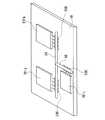
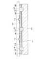
図1は本発明の第1実施形態に係る波長多重チップ間光インターコネクション回路を示す斜視図である。図2は図1に示す波長多重チップ間光インターコネクション回路の要部断面図である。
【0025】
基板10の表面には、複数の集積回路チップ(LSIチップ又はICチップ)201a,201b,201cが実装されている。集積回路チップ201a,201b,201cは、CPU、メモリ回路、映像信号処理回路、映像信号ドライブ回路、通信I/O、各種インターフェース回路、A/Dコンバータ、D/Aコンバータなどを構成するものである。なお、図1では3個の集積回路チップ201a,201b,201cが実装されているが、本発明はこれに限定されるものではない。基板10としては、ガラスエポキシ、セラミック、ガラス、プラスチック、半導体、ポリイミド、シリコンなど任意のものを適用することができる。
【0026】
基板10の表面における各集積回路チップ201a,201b,201cの近辺には、複数の微小タイル状素子200が接着剤などで貼り付けられている。微小タイル状素子200は、発光機能又は受光機能を備えた微小なタイル形状の半導体デバイスである。発光機能を備えた微小タイル状素子200は、面発光レーザ(VCSEL)、電界吸収変調内蔵のDFB(Distributed Feedback)レーザ又はLEDなどを備えるものとする。受光機能を有する微小タイル状素子は、例えばフォトダイオード又はフォトトランジスタなどを備えるものとする。また、例えば微小タイル状素子200は、厚さが20μm以下であり、縦横の大きさが数十μmから数百μmの板状部材とする。微小タイル状素子200の製造方法については、後で詳細に説明する。
【0027】
ここで、各微小タイル状素子200の発光機能又は受光機能は、波長選択性をもっている。例えば、波長λ1の光を放射する微小タイル状素子、波長λ2の光を放射する微小タイル状素子、波長λnの光を放射する微小タイル状素子、波長λ1の光を受光する微小タイル状素子、波長λ2の光を受光する微小タイル状素子、波長λnの光を受光する微小タイル状素が、それぞれ微小タイル状素子200として貼り付けられている。各微小タイル状素子200の波長選択性は、その微小タイル状素子200の発光面又は受光面に、特定の波長の光のみを透過させるカラーフィルタ又はバントバスフィルタをなす膜などを設けることで実現してもよい。
【0028】
また、基板10の表面には、光導波路材からなる光導波路30が設けられている。光導波路材としては透明樹脂又はゾルゲルガラスなどを適用することができる。そして、光導波路30は、各微小タイル状素子200を接続するように、すなわち各微小タイル状素子200の上を通るように形成されている。そこで、各微小タイル状素子200は、光導波路30によって光学的に接続される。したがって、ある微小タイル状素子200から放射された波長λ1の光信号は、光導波路30を伝播して、波長λ1の光を受光する微小タイル状素子200によって受信される。また、光導波路30は、図1に示すような分岐を設けてもよく、曲線形状にしてもよい。また図1では1つの光導波路30が設けられているが、1つの基板10に複数本の光導波路30を設けてもよい。
【0029】
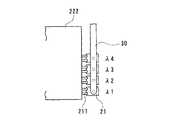
各集積回路チップ201a,201b,201cは、図2に示すように基板10の表面にフリップチップ実装されている。微小タイル状素子200は基板10に接着されている。微小タイル状素子200と電気的に接続するように電極211が設けられている。集積回路チップ201aはバンプ212などを介して電極211に接続されている。このように集積回路チップ201aと微小タイル状素子200が電気的に接続されている。電極211は、基板10表面に設けられバンプ212が接続するボンディングパッドと、微小タイル状素子200を接続する金属配線で構成してもよい。バンプ212と電極211は、直接接合に限定されず、ハンダや導電ペーストなどを介して接合してもよい。
【0030】
これらの構成により、例えば集積回路チップ201aから出力された電気信号(パルス信号)は、バンプ212及び電極211を経由して微小タイル状素子200に伝達する。その電気信号は、微小タイル状素子200によって例えば波長λ1の光パルス信号に変換されて光導波路30内に放射される。その波長λ1の光パルス信号は、光導波路30を伝播し集積回路チップ201b,201cにそれぞれ接続されている波長λ1の光を受光する微小タイル状素子200で電気信号に変換される。その電気信号は、集積回路チップ201b,201cにそれぞれ入力される。
【0031】
この動作と同様にして、集積回路チップ201aから出力された複数の電気信号は、集積回路チップ201aに接続されている複数の微小タイル状素子200によって波長λ1,λ2,λnの複数の光パルス信号に変換される。その複数の光パルス信号は、光導波路30を同時に伝播する。そして、波長λ1の光パルス信号は、集積回路チップ201b,201cにそれぞれ接続されている波長λ1の光を受光する微小タイル状素子200で電気信号に変換され、集積回路チップ201b,201cそれぞれに入力される。また、波長λ2の光パルス信号は、集積回路チップ201b,201cにそれぞれ接続されている波長λ2の光を受光する微小タイル状素子200で電気信号に変換され、集積回路チップ201b,201cそれぞれに入力される。また、波長λnの光パルス信号は、集積回路チップ201b,201cにそれぞれ接続されている波長λnの光を受光する微小タイル状素子200で電気信号に変換され、集積回路チップ201b,201cそれぞれに入力される。すなわち、各波長の光パルス信号は、クロストークすることなく、所望の微小タイル状素子200間で送受信される。
【0032】
したがって、本実施形態によれば、1つの光導波路30と複数の微小タイル状素子200を用いて、集積回路チップ201a,201b,201c同士間においてそれぞれ異なる波長の複数の光パルス信号を独立して並列に伝送する波長多重伝送をすることができる。そこで、本実施形態によれば、集積回路チップ201a,201b,201c同士間において極めて高速にデータ伝送することができ、コンパクトにかつ簡便に製造することができる波長多重チップ間光インターコネクション回路を提供することができる。
【0033】
また、上記実施形態では、集積回路チップ201a,201b,201c同士間でのデータ伝送に本発明を適用した例について説明したが、本発明はこれに限定されるものではなく、集積回路チップと基板10に設けられた回路との間に本発明に係る波長多重チップ間光インターコネクション回路を適用してもよい。
【0034】
(第2実施形態)
次に本発明の第2実施形態に係る波長多重チップ間光インターコネクション回路の応用例について図3から図5を参照して説明する。本実施形態はフラットパネルディスプレイ(FPD)のタイミングコントロール回路とドライバ回路とを光導波路30などで接続するものである。図3は本発明の第2実施形態に係る波長多重チップ間光インターコネクション回路の応用例であるフラットパネルディスプレイの回路図である。
【0035】
基板10は、フラットパネルディスプレイの構成部材となるものである。この基板10としては、ガラス又はプラスチックなどを適用することができる。基板10の上には、タイミングコントロール回路222と、複数(例えば4個)のデータ線ドライバ回路223−1,223−2,223−3,223−4と、複数(例えば4個)の走査線ドライバ回路224−1,224−2,224−3,224−4と、画素マトリクス(表示面)225とが設けられている。タイミングコントローラ回路222の入力端子には、映像ソース221(パーソナルコンピュータ、ビデオ、チューナなど)の出力端子が接続されている。
【0036】
タイミングコントローラ回路222、データ線ドライバ回路223−1,223−2,223−3,223−4及び走査線ドライバ回路224−1,224−2,224−3,224−4は、それぞれ集積回路チップで構成され、図1の集積回路チップ201a,201b,201cに相当するものである。したがって、タイミングコントローラ回路222、データ線ドライバ回路223−1,223−2,223−3,223−4及び走査線ドライバ回路224−1,224−2,224−3,224−4は、基板10上にフリップチップ実装されていることが好ましい。
【0037】
そして、タイミングコントロール回路222とデータ線ドライバ回路223−1,223−2,223−3,223−4を結ぶように、1つの光導波路30Aが基板10上に設けられている。この光導波路30Aは、上記第1実施形態の光導波路30に相当するものであり、データ線ドライバ回路223−1,223−2,223−3,223−4毎に分岐路を備えている。
【0038】
また、タイミングコントロール回路222と走査線ドライバ回路224−1,224−2,224−3,224−4を結ぶように、1つの光導波路30Bが基板10上に設けられている。この光導波路30Bは、上記第1実施形態の光導波路30に相当するものであり、走査線ドライバ回路224−1,224−2,224−3,224−4毎に分岐路を備えている。
【0039】
タイミングコントロール回路222は、光導波路30Aと光学的に接続された複数の発光機能を有する第1微小タイル状素子21Aを備えている。第1微小タイル状素子21Aは、上記第1実施形態における発光機能を有する微小タイル状素子200に相当するものである。そして第1微小タイル状素子21Aは、タイミングコントロール回路222の出力信号の一つであるデータ信号(電気信号)を光パルス信号に変換するものである。この複数(例えば4個)の第1微小タイル状素子21Aは、それぞれ波長λ1,λ2,λ3,λ4の光パルス信号を放射する。
【0040】
また、タイミングコントロール回路222は、光導波路30Bに光学的に接続された複数の発光機能を有する第1微小タイル状素子21Bを備えている。この第1微小タイル状素子21Bも上記第1実施形態における発光機能を有する微小タイル状素子200に相当するものである。したがって、この第1微小タイル状素子21Bも、タイミングコントロール回路222の出力手段となるものである。そして、第1微小タイル状素子21Bは、タイミングコントロール回路222の出力信号の一つである走査信号(電気信号)を光パルス信号に変換するものである。この複数(例えば4個)の第1微小タイル状素子21Bは、それぞれ波長λ1’,λ2’,λ3’,λ4’の光パルス信号を放射する。
【0041】
各データ線ドライバ回路223−1,223−2,223−3,223−4は光導波路30Aの分岐路と光学的に接続された受光機能を有する第2微小タイル状素子22Aを1つづつ備えている。この第2微小タイル状素子22Aは、上記第1実施形態における受光機能を有する微小タイル状素子200に相当するものである。したがって、この微小タイル状素子22Aは、データ線ドライバ回路223−1,223−2,223−3,223−4の入力手段となるものである。
【0042】
例えば第1のデータ線ドライバ回路223−1は、光導波路30Aを伝播する複数のデータ信号のうちで、波長λ1の光パルス信号を選択的に受信する第2微小タイル状素子22Aを備えている。第2のデータ線ドライバ回路223−2は、波長λ2の光パルス信号を選択的に受信する第2微小タイル状素子22Aを備えている。第3のデータ線ドライバ回路223−3は、波長λ3の光パルス信号を選択的に受信する第2微小タイル状素子22Aを備えている。第4のデータ線ドライバ回路223−4は、波長λ4の光パルス信号を選択的に受信する第2微小タイル状素子22Aを備えている。
【0043】
各走査線ドライバ回路224−1,224−2,224−3,224−4は、光導波路30Bの分岐路と光学的に接続された受光機能を有する第2微小タイル状素子22Bを1つづつ備えている。この第2微小タイル状素子22Bも、上記第1実施形態における受光機能を有する微小タイル状素子200に相当するものである。したがって、この微小タイル状素子22Bは、走査線ドライバ回路の入力手段となるものである。
【0044】
例えば、第1の走査線ドライバ回路224−1は、光導波路30Bを伝播する複数の走査信号のうちで、波長λ1’の光パルス信号を選択的に受信する第2微小タイル状素子22Bを備えている。第2の走査線ドライバ回路224−2は、波長λ2’の光パルス信号を選択的に受信する第2微小タイル状素子22Bを備えている。第3の走査線ドライバ回路224−3は、波長λ3’の光パルス信号を選択的に受信する第2微小タイル状素子22Bを備えている。第4の走査線ドライバ回路224−4は、波長λ3’の光パルス信号を選択的に受信する第2微小タイル状素子22Bを備えている。
【0045】
次に、上記構成のフラットパネルディスプレイの動作について説明する。まず映像ソース221から出力された映像信号は、タイミングコントロール回路222に入力される。タイミングコントロール回路222は、入力した映像信号を処理して例えば4種類のデータ信号と4種類の走査信号を生成する。このうち4種類のデータ信号は、4個の第1微小タイル状素子21Aによって波長λ1,λ2,λ3,λ4の4つの光パルス信号に変換される。また、4種類の走査信号は、4個の第1微小タイル状素子21Bによって波長λ1’,λ2’,λ3’,λ4’の4つの光パルス信号に変換される。
【0046】
波長λ1,λ2,λ3,λ4の4つの光パルス信号は、光導波路30Aに同時に入射し、その光導波路30Aのすみずみを伝播する。そこで、波長λ1の光パルス信号は、第1のデータ線ドライバ回路223−1に設けられた第2微小タイル状素子22Aで受信される。これと同時に、波長λ2の光パルス信号は、第2のデータ線ドライバ回路223−2に設けられた第2微小タイル状素子22Aで受信される。これと同時に、波長λ3の光パルス信号は、第3のデータ線ドライバ回路223−3に設けられた第2微小タイル状素子22Aで受信される。これと同時に、波長λ4の光パルス信号は、第4のデータ線ドライバ回路223−4に設けられた第2微小タイル状素子22Aで受信される。
【0047】
各データ線ドライバ回路223−1,223−2,223−3,223−4は、それぞれ第2微小タイル状素子22Aで所定波長の光パルス信号(データ信号)を電気信号に変換して入力する。そして、各データ線ドライバ回路223−1,223−2,223−3,223−4は、画素マトリクス225に配置されている複数のデータ線(図示せず)のうちで、割り当てられた複数のデータ線それぞれに、データ信号を出力する。
【0048】
また、波長λ1’,λ2’,λ3’,λ4’の4つの光パルス信号は、光導波路30Bに同時に入射し、その光導波路30Bのすみずみを伝播する。そこで、波長λ1’の光パルス信号は、第1の走査線ドライバ回路224−1に設けられた第2微小タイル状素子22Bで受信される。これと同時に、波長λ2’の光パルス信号は、第2の走査線ドライバ回路224−2に設けられた第2微小タイル状素子22Bで受信される。これと同時に、波長λ3’の光パルス信号は、第3の走査線ドライバ回路224−3に設けられた第2微小タイル状素子22Bで受信される。これと同時に、波長λ4’の光パルス信号は、第4の走査線ドライバ回路224−4に設けられた第2微小タイル状素子22Bで受信される。
【0049】
各走査線ドライバ回路224−1,224−2,224−3,224−4は、それぞれ第2微小タイル状素子22Bで所定波長の光パルス信号(走査信号)を電気信号に変換して入力する。そして、各走査線ドライバ回路224−1,224−2,224−3,224−4は、画素マトリクス225に配置されている複数の走査線(図示せず)のうちで、割り当てられた複数の走査線それぞれに、走査信号を出力する。
【0050】
各データ線ドライバ回路223−1,223−2,223−3,223−4から出力されたデータ信号と、各走査線ドライバ回路224−1,224−2,224−3,224−4から出力された走査信号とによって、画素マトリクス225の各画素が逐次駆動制御され、画素マトリクス225において映像が表示される。
【0051】
これらにより、本実施形態によれば、タイミングコントロール回路222とデータ線ドライバ回路223−1,223−2,223−3,223−4間を1本の光導波路30Aで波長多重接続し、タイミングコントロール回路222と走査線ドライバ回路224−1,224−2,224−3,224−4間を1本の光導波路30Bで波長多重接続したので、コンパクトでありながら、画素数が従来よりも多く、光画質なフラットパネルディスプレイを提供することができる。
【0052】
なお、画素マトリクス225に配置されている走査線及びデータ線は、従来のフラットパネルディスプレイで用いられているように電気配線で構成してもよいが、上記実施形態の光導波路30で構成してもよい。この構成とした場合、各データ線ドライバ回路223及び各走査線ドライバ回路224の出力部に発光機能をもつ微小タイル状素子を設けるとともに、各走査線及びデータ線から信号を受信する各画素の信号受信手段として、受光機能をもつ微小タイル状素子を設けることが好ましい。
【0053】
また、本実施形態によれば、信号伝達を光で行うので、FPDのように比較的配線距離の長くなるタイミングIC(タイミングコントロール回路222)と各ドライバIC(データ線ドライバ回路223、走査線ドライバ回路224)との間の接続においても、高速のデータ伝達が可能になる。
また、本実施形態によれば、映像信号などを光信号で伝送することができるので、画面からでる電磁波を大幅に低減することができ、電磁波障害(EMI)の発生を大幅に低減することができる。
【0054】
また、本実施形態のフラットパネルディスプレイにおいて、基板10上に、集積回路チップなどからなるCPU及び記憶手段などを形成してもよい。そのCPU及び記憶手段は、図1に示す集積回路チップ201a,201b,201cとして基板10上に実装することが好ましい。そして、各集積回路チップ201a,201b,201c同士間及びその集積回路チップとタイミングコントロール回路222間などでのデータ伝送は、光導波路30を用いることが好ましい。このようにすることにより、情報処理手段とフラットパネルディスプレイとが一体化したコンパクトで高性能なコンピュータシステムを提供することができる。
【0055】
上記実施形態では、第2微小タイル状素子22A,22B自身が受光波長選択性をもつものとしたが、本発明はこれに限定されるものではなく、光導波路30A,30Bの各分岐部31cに波長選択機能をもたせてもよい。例えば、各分岐部31c又は分岐路にバンドパスフィルタ又はカラーフィルタを設けてもよく、各分岐部31cに波長選択性ハーフミラーなどを設けてもよい。
【0056】
次に、本実施形態において、タイミングコントロール回路222をなす集積回路チップを基板10にフリップチップ実装した構成例について具体的に説明する。なお、下記の構成例と同様にして、データ線ドライバ回路223−1,223−2,223−3,223−4及び走査線ドライバ回路224−1,224−2,224−3,224−4などをなす集積回路チップを基板10にフリップチップ実装することができる。図4はタイミングコントロール回路222がフリップチップ実装された場合の構成例を示す要部断面図である。図5は図4に示す構成例の要部平面図である。
【0057】
タイミングコントロール回路222は、基板10上において集積回路チップ(ICチップ)としてフリップチップ実装されたものである。第1微小タイル状素子21は基板10に接着されている。第1微小タイル状素子21と電気的に接続するように電極211が設けられている。タイミングコントロール回路222はバンプ212などを介して電極211に接続されている。このようにタイミングコントロール回路222と第1微小タイル状素子21が電気的に接続されている。電極211は、基板10表面に設けられバンプ212が接続するボンディングパッドと、第1微小タイル状素子21を接続する金属配線で構成してもよい。バンプ212と電極211は、直接接合に限定されず、ハンダや導電ペーストなどを介して接合してもよい。
【0058】
タイミングコントロール回路222の入出力端子のいずれかは、バンプ212と電気的に接続されている。また、基板10上において、タイミングコントロール回路222の近辺には、図5に示すように、複数(例えば4個)の第1微小タイル状素子21が貼り付けられている。その複数の第1微小タイル状素子21を被うように、1本の光導波路30が設けられている。
【0059】
4個の第1微小タイル状素子21は、それぞれ波長λ1,λ2,λ3,λ4の光パルス信号を放射する。電極211は、各第1微小タイル状素子21毎に設けられ、その第1微小タイル状素子21と電気的に接続されている。バンプ212は、電極毎に設けられ、その電極と電気的に接続されている。
【0060】
このような構成により、例えばタイミングコントロール回路222で生成された4種類のデータ信号は、それぞれ各バンプ212に出力される。そのデータ信号は、各電極211を介して各第1微小タイル状素子21に入力され、波長λ1,λ2,λ3,λ4の光パルス信号とされて同時に光導波路30に放射される。
【0061】
本実施形態によれば、一般的なフリップチップ法によるタイミングIC(タイミングコントロール回路222)とドライバIC(データ線ドライバ回路223、走査線ドライバ回路224)の実装手法を用いることができ、従来の実装手法と整合しながら高速の光データ伝送を実現できる。これらにより、本実施形態によれば、1本の光導波路30を用いてコンパクトにかつ簡便に波長多重による光バスを構成することができる。
【0062】
(光インターコネクション回路)
次に、上記実施形態の波長多重チップ間光インターコネクション回路の要素となる光インターコネクション回路について詳細に説明する。
【0063】
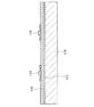
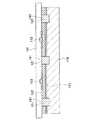
図6は本実施形態に係る光インターコネクション回路を示し、(a)は概略側面図であり、(b)は概略平面図である。本実施形態に係る光インターコネクション回路は、基板10の表面に接着された第1微小タイル状素子21及び第2微小タイル状素子22と、第1微小タイル状素子21と第2微小タイル状素子22を繋ぐように基板10の表面に形成された光導波路材からなる光導波路30とからなるものである。なお、図1から図5に示す上記実施形態と同一のものには同一の符号を付している。光導波路30をなす光導波路材としては、透明樹脂又はゾルゲルガラスを適用することができる。基板10としては、ガラスエポキシ、セラミック、プラスチック、ポリイミド、シリコン又はガラスなど任意のものを適用することができる。
【0064】
第1微小タイル状素子21は、発光機能をもつ発光部21aを備えている。第2微小タイル状素子22は、受光機能をもつ受光部22bを備えている。そして光導波路30をなす光導波路材は、少なくとも第1微小タイル状素子21の発光部21aと第2微小タイル状素子22の受光部22bを被うように形成されている。
【0065】
このような構成により、第1微小タイル状素子21の発光部21aから放射された光は、光導波路30を伝播し、第2微小タイル状素子22の受光部22bに到達する。そこで、発光部21aの発光動作を制御して光信号を発光部21aから放射すると、その光信号が光導波路30を伝播し、その光信号を受光部22bが検出することができる。
【0066】
また、第1微小タイル状素子21から放射された光信号は、光導波路30を伝播して第2微小タイル状素子22に入射するとともに、第2微小タイル状素子22の上を通過する。これにより、1個の第1微小タイル状素子21から複数個の第2微小タイル状素子22へ略同時に光信号を送信することができる。ここで、第2微小タイル状素子22の厚さを20μm以下とすることにより、基板との段差が十分小さくなるため、図6のように段差を乗り越えて連続的に光導波路30を形成できる。段差部において連続的に光導波路30を形成しても、段差が小さいため、散乱などの光の伝達損失はほとんど無視できる。そのため段差部に段差緩和のための特別な構造や光学素子を必要としない。よって低コストかつ簡便に作製できる。また、光導波路30をなす光導波路材の厚さを数十μm以下にすることができる。
【0067】
第1微小タイル状素子21は、例えば、LED、VCSEL(面発光レーザ)又は電界吸収変調器内蔵のDFBレーザを備えるものとする。発光デバイスとして、LEDはもっとも構造が単純で作製が容易であるが、光信号の変調速度が数百Mbps程度と遅い。これに対してVCSELは、10Gbpsを超える非常に高速な変調が可能であるうえ、しきい値電流が小さく発光効率が高いので低消費電力で駆動できる。DFBレーザは、変調速度は1Gbps程度と面発光レーザには及ばないものの、微小タイル形状の端部から基板10の平面と平行な方向、すなわち光導波路30に沿った方向へレーザ光を出射するため、面発光レーザより効率よく光信号を伝播することができる。
【0068】
第2微小タイル状素子22は、例えば、フォトダイオード又はフォトトランジスタを備えるものとする。ここで、フォトダイオードとしては、PIN型フォトダイオード、APD(アバランシェフォトダイオード)、MSM型フォトダイオードを用途に応じて選ぶことができる。APDは、光感度、応答周波数ともに高い。MSM型フォトダイオードは、構造が単純で増幅用トランジスタとともに集積化しやすい。
【0069】
また、受光素子からなる第3微小タイル状素子(図示せず)を第1微小タイル状素子21に重ねるように形成することもできる。こうすれば第1微小タイル状素子21の発光量を第3微小タイル状素子でモニタし、その値を第1微小タイル状素子21へフィードバックさせることでAPC機能を持たせることが可能となり、安定した光データ伝送を実現できる。あるいは第1微小タイル状素子21そのものにAPC機能を内蔵させてもよい。また、第2微小タイル状素子22は、検出した信号を増幅する回路などを備えることが望ましい。こうすることにより、装置をさらに高性能化することができる。
【0070】
そして、第1微小タイル状素子21及び第2微小タイル状素子22は、基板10に設けられた集積回路、又はEL表示回路、プラズマディスプレイ、液晶表示回路などの電子回路(図示せず)と電気的に接続されている。これにより、集積回路などからなるコンピュータシステムをコンパクトでありながら従来よりも高速にすることができる。また、基板10に設けられた平面ディスプレイなどの走査信号を本実施形態の光インターコネクション回路によって高速に伝送することができ、平面ディスプレイ装置における画面の大型化及び高品位化を促進することができる。
【0071】
図6においては、第1微小タイル状素子21と第2微小タイル状素子22がそれぞれ一つづつ、一本の光導波路30に結合されているが、第2微小タイル状素子22の個数は複数個であってもよい。この場合、一つの第1微小タイル状素子21(発光素子)から送信された光信号は、一本の光導波路30を伝播して、複数の第2微小タイル状素子22で同時に検出されることができる。これは一対多のバスラインと同じである。
【0072】
また、第1微小タイル状素子21と第2微小タイル状素子22ともに複数個であってもよい。ここで、各第1微小タイル状素子21は、放射する光の波長が異なるものとしてもよい。また、各第2微小タイル状素子22は、少なくとも1つの第1微小タイル状素子21が放射する光の波長に対応して、波長選択機能をもつ受光手段であることが好ましい。これらにより、複数の第1微小タイル状素子21からそれぞれ送信された複数の光信号が、1つの光導波路30を同時に伝播して、複数の第2微小タイル素子22それぞれに検出されることができる。したがって、複数の光信号を並列に送受信することができるバスを、簡易に構成することができる。
【0073】
また、光導波路30は、図6においては直線状に形成されているが、曲線状に形成する又は複数に分岐させることもできる。また、ループ状に形成してもかまわない。また、複数のタイル状素子を覆うようにシート状に形成してもよい。もちろん一つの基板10の表面に複数の組の第1微小タイル状素子21と第2微小タイル状素子22及び光導波路30を形成してもかまわない。さらに、基板10の表裏両面に第1微小タイル状素子21と第2微小タイル状素子22及び光導波路30を形成することもできる。
【0074】
次に、本実施形態に係る光インターコネクション回路の変形例について図7から図10を参照して説明する。本実施形態は、第1微小タイル状素子21及び第2微小タイル状素子22の近傍の光導波路30において、光を散乱する光散乱機構を備えている点が図6に示す構成と異なる。図7は本実施形態に係る光インターコネクション回路の変形例を示す概略側面図である。
【0075】
本光インターコネクション回路は、光導波路30をなす光導波路材における第1微小タイル状素子21及び第2微小タイル状素子22の近傍に、光散乱機構31aをなす光散乱粒子が分散されている。光散乱粒子としては、例えばシリカ粒子、ガラス粒子又は金属粒子などを用いる。この光散乱機構31aを備えた光導波路30は、例えばディスペンサあるいはインクジェットノズルなどから液滴を吐出する液滴吐出方式を用いる。具体的には、あるインクジェットノズルなどから液状の光導波路材(樹脂など)を所定部位に吐出するとともに、他のインクジェットノズルなどから光散乱粒子を含んだ液状の光導波路材を所定部位に吐出することで、光散乱機構31aを備えた光導波路30を形成する。
【0076】
また、光導波路30の構成材料としては、樹脂の他にゾルゲルガラスを適用することができる。ゾルゲルガラスの製法は、金属アルコキシドに酸を加えて加水分解した溶液などを所定部位に塗布し、熱などのエネルギーを加えてガラス化するものである。
【0077】
図8は本実施形態に係る光インターコネクション回路の他の変形例を示す概略側面図である。本光インターコネクション回路の光散乱機構31a’は、光散乱粒子を分散した樹脂又はガラスがドーム状に形成したドーム状光散乱機構である。この光散乱機構31a’(ドーム状光散乱機構)を覆うように光導波路30が形成されている。この光散乱機構31a’は、図7に示す光散乱機構31aよりも、その大きさ及び形状などが制御しやすいので、光導波路30と第1微小タイル状素子21又は第2微小タイル状素子22との光結合効率の容易な調整が可能となる。
【0078】
次に、光散乱機構31a’の製造方法について説明する。まず、インクジェット又はディスペンサなどを用い、光散乱粒子を含んだ液状の樹脂又は珪酸エチルなどの金属アルコキシドに酸を加え加水分解した溶液などを基板10の所定部位にドーム状に塗布する。次いで、その塗布した部位に熱などのエネルギーを加えてかかる溶液を硬化又はガラス化する。このようにしてドーム状の光散乱機構31a’を第1微小タイル状素子21又は第2微小タイル状素子22の上に形成する。次いで、ドーム状の光散乱機構31a’を覆うように透明樹脂又はゾルゲルガラスで線状の光導波路30を形成する。
【0079】
図9は本実施形態に係る光インターコネクション回路の他の変形例を示す概略側面図である。本光インターコネクション回路の光散乱機構31bは、光導波路30をなす光導波路材の表面に凹凸を設けた構成としている。この光散乱機構31bも第1微小タイル状素子21及び第2微小タイル状素子22の近傍に設けられている。ここで、光散乱機構31bをなす凹凸は、エンボス加工又はスタンパ転写などで形成する。
【0080】
図10は本実施形態に係る光インターコネクション回路の他の変形例を示し、(a)は概略側面図であり、(b)は概略平面図である。本光インターコネクション回路の光散乱機構31cは、光導波路30をなす線状の光導波路材の線幅及び高さを変化させた構成としている。すなわち、光導波路30において、第2微小タイル状素子22の受光部22bの近傍について光導波路材の線幅及び高さを小さく絞っている。
【0081】
光散乱機構31cを備えた光導波路30の製造方法について次に説明する。先ず、基板10の表面の所望位置に第1微小タイル状素子21及び第2微小タイル状素子22を接着する。次いで、基板10の表面全体、並びに第1微小タイル状素子21及び第2微小タイル状素子22の表面全体に撥液処理を施す。次いで、撥液処理した面における光導波路30を設ける領域に親液処理を施す。ここで、親液処理を施す領域は、線状であって第2微小タイル状素子22の受光部22bの近傍について線幅を絞ったパターンとする。なお、親液処理としては、例えば紫外線を照射することで行う。
【0082】
次いで、親液処理した領域内に、インクジェットノズルなどから液状の光導波路材を滴下する。すると、かかる滴下された光導波路材は、親液処理された領域において濡れ広がる作用を受け、撥液処理された領域からは弾き出される作用を受け、また表面張力なども作用する。そこでかかる光導波路材は、図10に示すような受光部22bの近傍で線幅が絞られた形状となる。
【0083】
上記のように、光導波路30における第1微小タイル状素子21の近傍に光散乱機構31a,31b,31cを設けることにより、第1微小タイル状素子21から放射された光信号がその光散乱機構31a,31b,31cで散乱され、光導波路全体に効率よく光信号を伝播させることができる。また、第2微小タイル状素子22の近傍に光散乱機構31a,31b,31cを設けることで、光導波路30を伝播してきた光信号が第2微小タイル状素子22の近傍で散乱され、光信号を第2微小タイル状素子22に効率よく入射させることができる。
【0084】
次に、本実施形態に係る光インターコネクション回路のさらなる変形例について図11から図13を参照して説明する。本実施形態は、光導波路30における第1微小タイル状素子21及び第2微小タイル状素子22の近傍、又は光導波路30の端部に、光を反射する光反射機構を備える点が上記実施形態と異なる。図11は、本実施形態に係る光インターコネクション回路の変形例を示し、(a)は概略側面図であり、(b)は概略平面図である。
【0085】
例えば、光導波路30をなす光導波路材の表面に金属膜を形成することで光反射機構32a,32bを設ける。また、光導波路30をなす光導波路材の表面に金属微粒子を含む塗料を塗布することで光反射機構32a,32bを設けてもよい。金属微粒子としては、銀、アルミニウム、マグネシウム、銅、ニッケル、チタン、クロム、亜鉛などの微粒子を適用することができる。光反射機構32a,32bをなす金属膜の形成及び金属微粒子を含む塗料の塗布は、インクジェットノズルなどから塗料などを吐出することで行ってもよい。また、光反射機構32a又は光反射機構32bは、光導波路30の全体に施してもかまわない。
【0086】
このような構成にすることにより、第1微小タイル状素子21から放射された光信号が光反射機構32aで光導波路30に沿う方向に反射され、その光信号の一部が光反射機構32bで第2微小タイル状素子22の方向に反射される。したがって、本実施形態によれば、光信号を効率よく伝播させることができる。
【0087】
図12は本実施形態に係る光インターコネクション回路の他の変形例を示し、(a)は概略側面図であり、(b)は概略平面図である。本光インターコネクション回路の光反射機構32cは、反射面を有する反射板が光導波路30の端部に貼り付けられた構成となっている。ここで、光反射機構32cの反射面は、基板10の表面に対して例えば45度の角度をもつように設けられている。
【0088】
また、本光インターコネクション回路では、2本の平行な光導波路30a,30bが設けられている。そして、光反射機構32cは、2本の光導波路30a,30bの一方端に設けら、光導波路30a,30bに共用される1枚の共通反射板となっている。そこで、2つの第1微小タイル状素子21からそれぞれ放射された光信号は、光反射機構32cによってそれぞれ光導波路30a,30bに沿う方向に反射される。したがって、本実施形態によれば、光信号を効率よく伝播させることができるとともに、効率よく光インターコネクション回路を製造することができる。
なお、図12に示す形態では、2本の光導波路30a,30bに共通の光反射機構32cを設けたが、3本以上の光導波路に共通の光反射機構32cを設けてもよい。
【0089】
図13は本実施形態に係る光インターコネクション回路の他の変形例を示し、(a)は概略側面図であり、(b)は概略平面図である。本光インターコネクション回路の光反射機構32d,32eは、グレーティングを施した板状の光学部品(グレーティング部品)である。光反射機構32dは第1微小タイル状素子21に被さるように、光反射機構32eは第2微小タイル状素子22に被さるように、光導波路30上に設置されている。
【0090】
ここで、光導波路30aと光導波路30bの間隔が比較的大きい場合は、図13に示すように各光導波路30a,30bに別個に光反射機構32eを取り付ける。光導波路30aと光導波路30bが接近しておりほぼ平行に配置されている場合は、図13に示すように光導波路30a,30bに共通な光反射機構32dを取り付けてもよい。
【0091】
上記図7から図13に示す光散乱機構及び光反射機構は、互いに組み合わせて用いるとより効果的である。
【0092】
(製造方法)
次に、上記実施形態に係る光インターコネクション回路における光導波路30の製造方法について、図14から図17を参照して説明する。図14は光導波路30の製造方法を示す模式側面図である。
【0093】
先ず、基板10の上面に上記第1微小タイル状素子及び第2微小タイル状素子を接着しておく。その後、光導波路30の製造工程に入る。そして、図14(a)に示すように、基板10の上面と第1微小タイル状素子及び第2微小タイル状素子(図示せず)の上面の全体に、液状の光硬化樹脂30cをコーティングする。このコーティングは、スピンコート法、ロールコート法、スプレイコート法などで行う。
【0094】
次いで液状の光硬化樹脂30cに対して、所望パターンのマスクを介して紫外線(UV)を照射する。これにより、液状の光硬化樹脂30cにおける所望領域だけが硬化しパターニングされる。そして、硬化していない樹脂を洗浄などにより除去することで、図14(b)に示すように、硬化された光導波路材からなる光導波路30dが形成される。
【0095】
図15は光導波路30の製造方法についての他の例を示す模式側面図である。先ず、基板10の上面に上記第1微小タイル状素子及び第2微小タイル状素子を接着しておく。その後、光導波路30の製造工程に入る。そして、図15(a)に示すように、基板10の上面と第1微小タイル状素子及び第2微小タイル状素子(図示せず)の上面全体に樹脂30eをコーティングして硬化させる。このコーティングは、スピンコート法、ロールコート法、スプレイコート法などで行う。次いで、樹脂30eにおける所望領域にレジストマスク41を形成する。このレジストマスク41の形成領域は光導波路30を形成する領域と同じである。
【0096】
次いで、図15(b)に示すように、レジストマスク41の上から基板10全体についてドライエッチング又はウエットエッチングを施し、レジストマスク41の下以外にある樹脂eを除去する。このようにフォトリソパターニングして、レジストマスク41を除去することで、光導波路材からなる光導波路30fが形成される。
【0097】
図16は光導波路30の製造方法についての他の例を示す模式側面図である。先ず、基板10の上面に上記第1微小タイル状素子及び第2微小タイル状素子を接着しておく。その後、光導波路30の製造工程に入る。そして、基板10の上面と第1微小タイル状素子及び第2微小タイル状素子(図示せず)の上面全体に、撥液処理を施して撥液表面51を設ける。
【0098】
次いで、図16(a)に示すように、撥液表面51における所望パターン領域に紫外線を照射することなどして、撥液表面51のなかに所望パターンの親液表面52を設ける。次いで、図16(b)に示すように、親液表面52のなかに、インクジェットノズルまたはディスペンサなどから液状の光導波路材30gを滴下する。光導波路材30gとしては、透明樹脂又はゾルゲルガラスを用いる。そして、基板10上に滴下された光導波路材30gを硬化させることで、光導波路材からなる光導波路30hが形成される。
ゾルゲルガラスで光導波路30gを形成する場合は、金属アルコキシドに酸を加えて加水分解した溶液などをインクジェットノズルまたはディスペンサなどから親液表面52に滴下する。次いで、滴下した溶液に熱などのエネルギーを加えてガラス化し光導波路30hとする。
【0099】
図17は光導波路30の製造方法についての他の例を示す模式側面図である。先ず、基板10の上面に上記第1微小タイル状素子及び第2微小タイル状素子を接着しておく。その後、光導波路30の製造工程に入る。そして、図17(a)に示すように、基板10の上面並びに第1微小タイル状素子及び第2微小タイル状素子の上面であって、光導波路30を設けようとする領域を被うように、液状の樹脂30iを塗布する。
【0100】
次いで、光導波路30のパターン形状52をもつ型であるスタンパ51を、基板10の上方から基板10の表面に押し付ける。次いで、図17(b)に示すように、基板10の表面からスタンパ51を持ち上げる。これらにより、スタンパ51を用いたパターン転写法により、基板10上に所望パターン形状の光導波路材からなる光導波路30jが形成される。
【0101】
光導波路30の製造方法は、上記図14から図17に示す方法以外に、次に述べる方法を用いてもよい。例えば、スクリーン印刷又はオフセット印刷などの印刷法を用いて、光導波路30をなす光導波路材を設けてもよい。また、スリット状の隙間から液状の樹脂を吐出するスリットコート法を用いて、光導波路30をなす光導波路材を設けてもよい。スリットコート法としては、毛細管現象を用いて樹脂などの所望部材を基板10に塗布する手法を採用してもよい。
【0102】
(微小タイル状素子の製造方法)
次に、上記第1微小タイル状素子21及び第2微小タイル状素子22をなす微小タイル状素子の製造方法について図18から図27を参照して説明する。本実施形態の微小タイル状素子は、エピタキシャルリフトオフ法を基礎とする手法で作製される。本製造方法では、微小タイル状素子としての化合物半導体デバイス(化合物半導体素子)を基板となるシリコン・LSIチップ上に接合する場合について説明するが、半導体デバイスの種類及びLSIチップの種類に関係なく本発明を適用することができる。なお、本実施形態における「半導体基板」とは、半導体物資から成る物体をいうが、板形状の基板に限らず、どのような形状であっても半導体物資であれば「半導体基板」に含まれる。
【0103】
<第1工程>
図18は微小タイル状素子の製造方法の第1工程を示す概略断面図である。図18において、基板110は、半導体基板であり、例えばガリウム・ヒ素化合物半導体基板とする。基板110における最下位層には、犠牲層111を設けておく。犠牲層111は、アルミニウム・ヒ素(AlAs)からなり、厚さが例えば数百nmの層である。
例えば、犠牲層111の上層には機能層112を設ける。機能層112の厚さは、例えば1μmから10(20)μm程度とする。そして、機能層112において半導体デバイス(半導体素子)113を作成する。半導体デバイス113としては、例えば発光ダイオード(LED)、面発光レーザ(VCSEL)、フォトダイオード(PD)、DFBレーザなどが挙げられる。これらの半導体デバイス113は、何れも基板110上に多層のエピタキシャル層を積層して素子が形成されたものである。また、各半導体デバイス113には、電極も形成し、動作テストも行う。
【0104】
<第2工程>
図19は微小タイル状素子の製造方法の第2工程を示す概略断面図である。本工程においては、各半導体デバイス113を分割するように分離溝121を形成する。分離溝121は、少なくとも犠牲層111に到達する深さをもつ溝とする。例えば、分離溝の幅及び深さともに、10μmから数百μmとする。また、分離溝121は、後述するところの選択エッチング液が当該分離溝121を流れるように、行き止まりなく繋がっている溝とする。さらに、分離溝121は、碁盤のごとく格子状に形成することが好ましい。
また、分離溝121相互の間隔を数十μmから数百μmとすることで、分離溝121によって分割・形成される各半導体デバイス113のサイズを、数十μmから数百μm四方の面積をもつものとする。分離溝121の形成方法としては、フォトリソグラフィとウェットエッチングによる方法、またはドライエッチングによる方法を用いる。また、クラックが基板に生じない範囲でU字形溝のダイシングで分離溝121を形成してもよい。
【0105】
<第3工程>
図20は微小タイル状素子の製造方法の第3工程を示す概略断面図である。本工程においては、中間転写フィルム131を基板110の表面(半導体デバイス113側)に貼り付ける。中間転写フィルム131は、表面に粘着剤が塗られたフレキシブルな帯形状のフィルムである。
【0106】
<第4工程>
図21は微小タイル状素子の製造方法の第4工程を示す概略断面図である。本工程においては、分離溝121に選択エッチング液141を注入する。本工程では、犠牲層111のみを選択的にエッチングするために、選択エッチング液141として、アルミニウム・ヒ素に対して選択性が高い低濃度の塩酸を用いる。
【0107】
<第5工程>
図22は微小タイル状素子の製造方法の第5工程を示す概略断面図である。本工程においては、第4工程での分離溝121への選択エッチング液141の注入後、所定時間の経過により、犠牲層111のすべてを選択的にエッチングして基板110から取り除く。
【0108】
<第6工程>
図23は微小タイル状素子の製造方法の第6工程を示す概略断面図である。第5工程で犠牲層111が全てエッチングされると、基板110から機能層112が切り離される。そして、本工程において、中間転写フィルム131を基板110から引き離すことにより、中間転写フィルム131に貼り付けられている機能層112を基板110から引き離す。
これらにより、半導体デバイス113が形成された機能層112は、分離溝121の形成及び犠牲層111のエッチングによって分割されて、所定の形状(例えば、微小タイル形状)の半導体素子(上記実施形態の「微小タイル状素子」)とされ、中間転写フィルム131に貼り付け保持されることとなる。ここで、機能層の厚さが例えば1μmから8μm、大きさ(縦横)が例えば数十μmから数百μmであるのが好ましい。
【0109】
<第7工程>
図24は微小タイル状素子の製造方法の第7工程を示す概略断面図である。本工程においては、(微小タイル状素子161が貼り付けられた)中間転写フィルム131を移動させることで、最終基板171の所望の位置に微小タイル状素子161をアライメントする。ここで、最終基板171は、例えば、シリコン半導体(図1における基板10)からなり、LSI領域172が形成されている。また、最終基板171の所望の位置には、微小タイル状素子161を接着するための接着剤173を塗布しておく。
【0110】
<第8工程>
図25は微小タイル状素子の製造方法の第8工程を示す概略断面図である。本工程においては、最終基板171の所望の位置にアライメントされた微小タイル状素子161を、中間転写フィルム131越しに裏押しピン181で押しつけて最終基板171に接合する。ここで、所望の位置には接着剤173が塗布されているので、その最終基板171の所望の位置に微小タイル状素子161が接着される。
【0111】
<第9工程>
図26は微小タイル状素子の製造方法の第9工程を示す概略断面図である。本工程においては、中間転写フィルム131の粘着力を消失させて、微小タイル状素子161から中間転写フィルム131を剥がす。
中間転写フィルム131の粘着剤は、紫外線(UV)又は熱により粘着力が消失するものにしておく。UV硬化性の粘着剤とした場合は、裏押しピン181を透明な材質にしておき、裏押しピン181の先端から紫外線(UV)を照射することで中間転写フィルム131の粘着力を消失させる。熱硬化性の接着剤とした場合は、裏押しピン181を加熱すればよい。あるいは第6工程の後で、中間転写フィルム131を全面紫外線照射するなどして粘着力を全面消失させておいてもよい。粘着力が消失したとはいえ実際には僅かに粘着性が残っており、微小タイル状素子161は非常に薄く軽いので中間転写フィルム131に保持される。
【0112】
<第10工程>
本工程は、図示していない。本工程においては、加熱処理などを施して、微小タイル状素子161を最終基板171に本接合する。
【0113】
<第11工程>
図27は微小タイル状素子の製造方法の第11工程を示す概略断面図である。本工程においては、微小タイル状素子161の電極と最終基板171上の回路を配線191により電気的に繋ぎ、一つのLSIチップなど(光インターコネクション回路用の集積回路チップ)を完成させる。最終基板171としては、シリコン半導体のみならず、石英基板又はプラスチックフィルムを適用してもよい。
【0114】
(応用例)
以下、本発明に係る波長多重チップ間光インターコネクション回路の応用例について説明する。
例えば上記実施形態の波長多重チップ間光インターコネクション回路をオプトエレクトロニクス集積回路システムの信号伝送手段として用いる。オプトエレクトロニクス集積回路システムとしては、コンピュータが挙げられる。そして、CPUをなす集積回路チップ及び記憶装置などをなす集積回路チップを基板10上に実装する。そして、CPU内及び記憶装置内での信号処理は電気信号を用いて行うが、集積回路チップ相互間などでのデータ伝送を上記実施形態の波長多重チップ間光インターコネクション回路を適用する。
【0115】
これらにより、本応用例によれば、簡易な構成でありながら、コンピュータの処理速度のボトルネックとなっているバスにおける信号伝達速度を従来よりも大幅に高めることが可能となる。また、本応用例によれば、コンピュータシステムなどを大幅に小型化及び高性能化することが可能となる。
【0116】
(電子機器)
上記実施形態の波長多重チップ間光インターコネクション回路又はフラットパネルディスプレイを備えた電子機器の例について説明する。
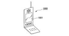
図28は、携帯電話の一例を示した斜視図である。図28において、符号1000は上記の波長多重チップ間光インターコネクション回路を用いた携帯電話本体を示し、符号1001は上記のフラットパネルディスプレイ(電気光学装置)を用いた表示部を示している。
【0117】
図29は、腕時計型電子機器の一例を示した斜視図である。図29において、符号1100は上記の波長多重チップ間光インターコネクション回路を用いた時計本体を示し、符号1101は上記のフラットパネルディスプレイ(電気光学装置)を用いた表示部を示している。
【0118】
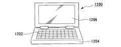
図30は、ワープロ、パソコンなどの携帯型情報処理装置の一例を示した斜視図である。図30において、符号1200は情報処理装置、符号1202はキーボードなどの入力部、符号1204は上記の波長多重チップ間光インターコネクション回路を用いた情報処理装置本体、符号1206は上記のフラットパネルディスプレイ(電気光学装置)を用いた表示部を示している。
【0119】
図28から図30に示す電子機器は、上記実施形態の波長多重チップ間光インターコネクション回路又はフラットパネルディスプレイを備えているので、表示品位に優れ、特に、高速応答で明るい大きな画面の表示部を備えた電子機器を実現することができる。また、上記実施形態の波長多重チップ間光インターコネクション回路を用いることによって、従来のものよりも電子機器を薄型化及び小型化することができる。さらにまた、上記実施形態の波長多重チップ間光インターコネクション回路を用いることによって、製造コストを従来のものよりも低減することができる。
【0120】
なお、本発明の技術範囲は上記実施形態に限定されるものではなく、本発明の趣旨を逸脱しない範囲において種々の変更を加えることが可能であり、実施形態で挙げた具体的な材料や構成などはほんの一例に過ぎず適宜変更が可能である。
【図面の簡単な説明】
【図1】 本発明の第1実施形態に係る回路を示す斜視図である。
【図2】 同上の回路の要部断面図である。
【図3】 本発明の第2実施形態に係るFDPの回路図である。
【図4】 同上の回路の要部断面図である。
【図5】 同上の回路の要部平面図である。
【図6】 本発明の実施形態に係る回路要素の側面図と平面図である。
【図7】 同上の回路要素の変形例を示す側面図である。
【図8】 同上の回路要素の変形例を示す側面図である。
【図9】 同上の回路要素の変形例を示す側面図である。
【図10】 同上の回路要素の変形例を示す側面図と平面図である。
【図11】 同上の回路要素の変形例を示す側面図と平面図である。
【図12】 同上の回路要素の変形例を示す側面図と平面図である。
【図13】 同上の回路要素の変形例を示す側面図と平面図である。
【図14】 本発明の実施形態に係る製造方法を示す模式側面図である。
【図15】 本発明の実施形態の他の製造方法を示す模式側面図である。
【図16】 本発明の実施形態の他の製造方法を示す模式側面図である。
【図17】 本発明の実施形態の他の製造方法を示す模式側面図である。
【図18】 微小タイル状素子の製法の第1工程を示す概略断面図である。
【図19】 同上の製法の第2工程を示す概略断面図である。
【図20】 同上の製法の第3工程を示す概略断面図である。
【図21】 同上の製造方法の第4工程を示す概略断面図である。
【図22】 同上の製造方法の第5工程を示す概略断面図である。
【図23】 同上の製造方法の第6工程を示す概略断面図である。
【図24】 同上の製造方法の第7工程を示す概略断面図である。
【図25】 同上の製造方法の第8工程を示す概略断面図である。
【図26】 同上の製造方法の第9工程を示す概略断面図である。
【図27】 同上の製造方法の第11工程を示す概略断面図である。
【図28】 本実施形態の回路を備えた電子機器の一例を示す図である。
【図29】 本実施形態の回路を備えた電子機器の一例を示す図である。
【図30】 本実施形態の回路を備えた電子機器の一例を示す図である。
【符号の説明】
10…基板、21,21A,21B…第1微小タイル状素子、21a…発光部、22,22A,22B…第2微小タイル状素子、22b…受光部、30,30A,30B…光導波路、31c…分岐部、200…微小タイル状素子、201a,201b,201c…集積回路チップ、211…電極、212…バンプ、222…タイミングコントロール回路、223−1,223−2,223−3,223−4…データ線ドライバ回路、224−1,224−2,224−3,224−4…走査線ドライバ回路、225…画素マトリクス[0001]
BACKGROUND OF THE INVENTION
The present invention relates to an optical interconnection circuit between wavelength multiplexing chips, an electro-optical device, and an electronic apparatus.
[0002]
[Prior art]
In recent years, as a flat display device, an electroluminescence panel (ELP), a plasma display panel (PDP), a liquid crystal display device (LCD), and the like are used. In these flat display devices, a technique for using light for signal transmission has been studied in order to eliminate signal delays associated with an increase in size and capacity (for example, see Patent Document 1).
[0003]
[Patent Document 1]
Japanese Patent Laid-Open No. 5-100246
[0004]
In addition, the operation speed (operation clock) inside the CPU is increasing year by year due to the miniaturization of the internal structure of the integrated circuit. However, the signal transmission speed in the bus connecting the CPU and peripheral devices such as a storage device is almost reaching its limit, which is a bottleneck in computer processing speed. If signal transmission on this bus can be performed using optical signals, the limit of the processing speed of the computer can be significantly increased.
[0005]
In order to transmit data using an optical signal, an optical transmission unit that transmits the optical signal emitted from the light source to a predetermined location and inputs it to a light receiving element or the like is required. Conventionally, as such an optical transmission means, there is a technique using an optical fiber or a technique using an optical waveguide formed on a substrate.
[0006]
[Problems to be solved by the invention]
However, when an optical fiber is used as an optical transmission means, connection with optical components such as a light emitting element and a light receiving element becomes complicated, and it takes a lot of cost and time to manufacture, and it is difficult to reduce the size of the optical transmission means. There is a problem of becoming.
[0007]
On the other hand, it is conceivable to simplify the connection between the light transmission medium, the light emitting element, the light receiving element, and the like by using an optical waveguide formed on the substrate. However, at present, an input / output structure suitable for this optical waveguide has not yet been found, and an optical transmission means that has been miniaturized and easily manufactured so as to be applicable to a flat display device or a computer has been realized. Absent.
[0008]
The present invention has been made in view of the above circumstances, and can increase the signal transmission speed and can be easily miniaturized, and can be easily manufactured. An object is to provide an electro-optical device and an electronic apparatus.
[0009]
[Means for Solving the Problems]
In order to achieve the above object, an optical interconnection circuit between wavelength multiplexing chips of the present invention is provided on a substrate, and includes a micro tile-like element having a light emitting function or a light receiving function having wavelength selectivity. It is characterized by having.
According to the present invention, an optical signal having a desired wavelength can be transmitted and received by a micro tile element having wavelength selectivity. Therefore, according to the present invention, for example, a plurality of optical signals having different wavelengths can be transmitted / received simultaneously using a plurality of micro tile elements, and wavelength division multiplexing transmission can be performed using one optical communication path.
In addition, according to the present invention, the micro tile element can be formed into a very small shape (for example, having an area of several hundred μm square or less and a thickness of several tens of μm or less), and is very compact. Therefore, it is possible to provide a wavelength multiplexing transmission means that can be used as a data transmission means between integrated circuit chips and can be easily manufactured.
[0010]
The wavelength-multiplexed chip optical interconnection circuit of the present invention preferably includes an optical waveguide provided on the substrate and optically connected to the micro tile-like element.
According to the present invention, for example, by providing an optical waveguide made of a transparent resin so as to pass through an upper portion of a micro tile-shaped element attached using an adhesive or the like at a desired position on a substrate, radiation from the micro tile-shaped element is achieved. Light or incident light on the micro tile element can be propagated in the optical waveguide. Therefore, according to the present invention, a compact wavelength multiplexing transmission means can be provided easily.
[0011]
In the wavelength-multiplexed chip optical interconnection circuit of the present invention, it is preferable that the optical waveguide has a resin and a branch path.
According to the present invention, an optical waveguide having a branch path can be simply configured using a resin. In addition, according to the present invention, since the optical waveguide includes a branch path, a plurality of micro tile-like elements arranged on the substrate can be easily dispersed with respect to one optical waveguide that is optically connected. Can be optically connected. Therefore, according to the present invention, an optical signal can be efficiently propagated in an optical waveguide to which a plurality of micro tile elements are connected, and the optical coupling efficiency in the optical waveguide can be increased.
[0012]
In the wavelength-multiplexed chip optical interconnection circuit of the present invention, it is preferable that a plurality of the optical waveguides are provided on the substrate.
According to the present invention, by using a plurality of optical waveguides, it is possible to easily increase the number of optical signals (wavelengths) that can be simultaneously transmitted and received, and it is possible to simply provide a higher-speed signal transmission means.
[0013]
Also, the wavelength-multiplexed chip optical interconnection circuit of the present invention has a light emitting function in which a plurality of the micro tile-like elements having a light emitting function are optically connected to one optical waveguide. The plurality of micro tile-like elements preferably have different emission wavelengths.
According to the present invention, a plurality of micro tile elements can be arranged on a substrate close to or in close proximity to each other, and an extremely compact optical multiplexed signal transmission means can be provided simply.
[0014]
In the wavelength-multiplexing chip optical interconnection circuit according to the present invention, it is preferable that a plurality of micro tile elements having the light emitting function simultaneously input light pulse signals having a plurality of light emitting wavelengths into one optical waveguide. .
According to the present invention, it is possible to simply provide an extremely compact optical multiplex signal transmission means by using one optical waveguide and a plurality of micro tile elements.
[0015]
In the wavelength-division-chip optical interconnection circuit of the present invention, the plurality of micro tile elements having a light receiving function are optically connected to one optical waveguide, and the light receiving function is provided. It is preferable that the plurality of micro tile elements have different light receiving wavelengths.
According to the present invention, there are a plurality of micro tile elements connected to the same optical waveguide, and the plurality of micro tile elements having a light receiving function are addressed to their own data (specific wavelength without crosstalk). Can be selectively received.
[0016]
Further, in the optical interconnection circuit between wavelength multiplexing chips of the present invention, an integrated circuit chip is mounted on the substrate, and the integrated circuit chip and the micro tile-like element are electrically connected by wiring on the substrate. It is preferable.
According to the present invention, input / output signals of an integrated circuit chip can be converted from an electrical signal to an optical signal or from an optical signal to an electrical signal by a micro tile element. Therefore, according to the present invention, the data transmission between the integrated circuit chip and other circuits can be extremely speeded up with an extremely compact and simple structure.
[0017]
In the optical interconnection circuit between wavelength multiplexing chips of the present invention, it is preferable that the integrated circuit chip is flip-chip mounted on the substrate.
According to the present invention, an integrated circuit chip can be easily and compactly mounted on a substrate. For example, a bonding pad functioning as an electrode or the like is formed on the substrate surface, a bump of a conductive conductor is formed on the bonding pad, and an integrated circuit chip can be flip-chip mounted on the bump.
[0018]
In the wavelength-division-chip optical interconnection circuit of the present invention, the substrate is a constituent element of a flat panel display, and at least a timing control integrated circuit and a driver integrated circuit are integrated on the substrate as the integrated circuit chip. Each circuit is mounted, and the optical waveguide is preferably provided so as to connect the timing control integrated circuit and the driver integrated circuit.
According to the present invention, in a flat panel display, a timing control circuit for generating a signal (data signal, scanning signal, etc.) for controlling each pixel based on a video signal, and a signal output from the timing control circuit are received and amplified. For example, a driver integrated circuit (data line driver integrated circuit, scanning line driver integrated circuit) that drives each pixel can be connected by an optical waveguide. Here, a plurality of types of data signals and scanning signals can be transmitted simultaneously with one optical waveguide. Therefore, according to the present invention, it is possible to transmit a data signal, a scanning signal, and the like at a very high speed while being a compact flat panel display, and to provide a display device having a higher number of pixels and higher image quality than before. it can.
In addition, according to the present invention, a micro tile element having a light emitting function can be driven with a simple driver, so that the circuit configuration of the flat panel display can be simplified and the manufacturing cost can be reduced. .
In addition, according to the present invention, since an image signal or the like can be transmitted as an optical signal, electromagnetic waves emitted from the screen can be greatly reduced, and occurrence of electromagnetic interference (EMI) can be greatly reduced. .
[0019]
In the wavelength-division-chip optical interconnection circuit according to the present invention, it is preferable that a plurality of the driver integrated circuits are mounted on the substrate, and the optical waveguide includes a branch path for each of the plurality of driver integrated circuits. .
According to the present invention, a data signal, a scanning signal, or the like incident on one optical waveguide from the timing control circuit can be transmitted to each driver integrated circuit via each branch path. Therefore, according to the present invention, the optical coupling efficiency of the optical waveguide can be increased, and the configuration of the flat panel display can be further simplified.
[0020]
In the wavelength-multiplexed chip optical interconnection circuit according to the present invention, the timing control integrated circuit includes a plurality of micro tile elements having a light emission function, and the plurality of micro tile elements having the light emission function are different. It is preferable that light of a wavelength is emitted and optically connected to the common optical waveguide.
According to the present invention, the timing control circuit is electrically connected to a plurality of micro tile elements that emit light of different wavelengths (for example, wavelengths λ1, λ2,. Optical signals (data signal, scanning signal, etc.) can be transmitted simultaneously.
[0021]
In the wavelength-multiplexed chip optical interconnection circuit of the present invention, it is preferable that the plurality of driver integrated circuits include the micro tile elements having different light receiving wavelengths.
According to the present invention, a plurality of optical signals (data signals, scanning signals, etc., for example, wavelengths λ1, λ2,... Λn) are propagated through the optical waveguide so that each driver integrated circuit has a desired optical signal (wavelengths λ1, λ2,. Can be received). Therefore, each driver integrated circuit can receive an optical signal addressed to itself from among a plurality of optical signals that propagate simultaneously through one optical waveguide.
[0022]
The electro-optical device according to the present invention includes the optical interconnection circuit between the wavelength multiplexing chips.
According to the present invention, in an electro-optical device such as a liquid crystal display device, an electroluminescence panel, and a plasma display, a timing control circuit, a driver circuit, and the like can be configured by the wavelength-multiplexed chip optical interconnection circuit. Therefore, according to the present invention, the scanning signal and data signal of the electro-optical device can be transmitted by the optical interconnection circuit between the wavelength multiplexing chips, and each pixel can be driven and controlled at high speed. A large screen, high quality, and further compactness can be realized.
[0023]
An electronic apparatus according to the present invention includes the optical interconnection circuit between the wavelength multiplexing chips.
According to the present invention, an electronic apparatus including a module in which a CPU, a memory circuit, and the like are configured by the integrated circuit chip and each chip is connected by the optical interconnection circuit between the wavelength division multiplexing chips is used. A compact and high-performance electronic device that can perform signal processing at high speed and can be provided at low cost.
In addition, according to the present invention, for example, by applying an optical interconnection circuit between wavelength multiplexing chips to a display device, a compact electronic device that can display a high-quality image can be provided at low cost.
[0024]
DETAILED DESCRIPTION OF THE INVENTION
Hereinafter, an optical interconnection circuit between wavelength multiplexing chips according to an embodiment of the present invention will be described with reference to the drawings.
(First embodiment)
FIG. 1 is a perspective view showing an optical interconnection circuit between wavelength division multiplexing chips according to a first embodiment of the present invention. FIG. 2 is a cross-sectional view of a principal part of the optical interconnection circuit between wavelength multiplexing chips shown in FIG.
[0025]
A plurality of integrated circuit chips (LSI chips or IC chips) 201a, 201b, 201c are mounted on the surface of the
[0026]
In the vicinity of each
[0027]
Here, the light emitting function or the light receiving function of each
[0028]
An
[0029]
Each
[0030]
With these configurations, for example, an electrical signal (pulse signal) output from the
[0031]
In the same manner as this operation, a plurality of electrical signals output from the
[0032]
Therefore, according to the present embodiment, by using one
[0033]
In the above embodiment, the example in which the present invention is applied to the data transmission between the
[0034]
(Second Embodiment)
Next, application examples of the wavelength multiplexing chip-to-chip optical interconnection circuit according to the second embodiment of the present invention will be described with reference to FIGS. In this embodiment, a timing control circuit and a driver circuit of a flat panel display (FPD) are connected by an
[0035]
The
[0036]
The
[0037]
One
[0038]
In addition, one
[0039]
The
[0040]
Further, the
[0041]
Each of the data line driver circuits 223-1, 223-2, 223-3 and 223-4 includes one second
[0042]
For example, the first data line driver circuit 223-1 includes a second
[0043]
Each of the scanning line driver circuits 224-1, 224-2, 224-3 and 224-4 includes one second
[0044]
For example, the first scanning line driver circuit 224-1 includes a second
[0045]
Next, the operation of the flat panel display configured as described above will be described. First, the video signal output from the
[0046]
The four optical pulse signals of wavelengths λ1, λ2, λ3, and λ4 are simultaneously incident on the
[0047]
Each of the data line driver circuits 223-1, 223-2, 223-3, and 223-4 converts an optical pulse signal (data signal) having a predetermined wavelength into an electrical signal by the second
[0048]
Also, the four optical pulse signals of wavelengths λ1 ′, λ2 ′, λ3 ′, and λ4 ′ are simultaneously incident on the
[0049]
Each of the scanning line driver circuits 224-1, 224-2, 224-3, and 224-4 converts an optical pulse signal (scanning signal) having a predetermined wavelength into an electrical signal and inputs it by the second
[0050]
Data signals output from the data line driver circuits 223-1, 223-2, 223-3 and 223-4, and output from the scanning line driver circuits 224-1, 224-2, 224-3 and 224-4 Each pixel of the
[0051]
As a result, according to the present embodiment, the
[0052]
The scanning lines and the data lines arranged in the
[0053]
In addition, according to the present embodiment, since signal transmission is performed by light, a timing IC (timing control circuit 222) and a driver IC (data line driver circuit 223, scanning line driver) that have a relatively long wiring distance, such as an FPD. Even in the connection with the circuit 224), high-speed data transmission is possible.
Further, according to the present embodiment, since an image signal or the like can be transmitted as an optical signal, electromagnetic waves emitted from the screen can be greatly reduced, and occurrence of electromagnetic interference (EMI) can be greatly reduced. it can.
[0054]
In the flat panel display of this embodiment, a CPU and a storage unit made of an integrated circuit chip or the like may be formed on the
[0055]
In the above embodiment, the second
[0056]
Next, in the present embodiment, a configuration example in which the integrated circuit chip forming the
[0057]
The
[0058]
One of the input / output terminals of the
[0059]
The four first
[0060]
With such a configuration, for example, four types of data signals generated by the
[0061]
According to this embodiment, it is possible to use a mounting method of a timing IC (timing control circuit 222) and a driver IC (data line driver circuit 223, scanning line driver circuit 224) by a general flip chip method. High-speed optical data transmission can be realized while matching with the method. Thus, according to the present embodiment, an optical bus by wavelength multiplexing can be configured in a compact and simple manner using a single
[0062]
(Optical interconnection circuit)
Next, the optical interconnection circuit that is an element of the optical interconnection circuit between wavelength multiplexing chips of the above embodiment will be described in detail.
[0063]
FIG. 6 shows an optical interconnection circuit according to the present embodiment, where (a) is a schematic side view and (b) is a schematic plan view. The optical interconnection circuit according to the present embodiment includes a first
[0064]
The first
[0065]
With such a configuration, the light emitted from the
[0066]
The optical signal radiated from the first
[0067]
The first micro tile-shaped
[0068]
The second micro tile-shaped
[0069]
In addition, a third micro tile element (not shown) made of a light receiving element can be formed so as to overlap the first
[0070]
The first
[0071]
In FIG. 6, the first
[0072]
Further, a plurality of first
[0073]
Moreover, although the
[0074]
Next, modified examples of the optical interconnection circuit according to the present embodiment will be described with reference to FIGS. This embodiment is different from the configuration shown in FIG. 6 in that the
[0075]
In the present optical interconnection circuit, light scattering particles forming the
[0076]
As a constituent material of the
[0077]
FIG. 8 is a schematic side view showing another modification of the optical interconnection circuit according to the present embodiment. The
[0078]
Next, a method for manufacturing the
[0079]
FIG. 9 is a schematic side view showing another modification of the optical interconnection circuit according to the present embodiment. The
[0080]
FIG. 10 shows another modification of the optical interconnection circuit according to the present embodiment, in which (a) is a schematic side view and (b) is a schematic plan view. The
[0081]
Next, a manufacturing method of the
[0082]
Next, a liquid optical waveguide material is dropped from an inkjet nozzle or the like into the lyophilic region. Then, the dropped optical waveguide material is subjected to an action of wetting and spreading in the lyophilic area, an action of being ejected from the lyophobic area, and surface tension and the like. Therefore, the optical waveguide material has a shape with a narrowed line width in the vicinity of the
[0083]
As described above, by providing the
[0084]
Next, further modifications of the optical interconnection circuit according to the present embodiment will be described with reference to FIGS. In the present embodiment, a light reflection mechanism that reflects light is provided in the vicinity of the first
[0085]
For example, the
[0086]
With this configuration, the optical signal emitted from the first micro tile-
[0087]
FIG. 12 shows another modification of the optical interconnection circuit according to the present embodiment, in which (a) is a schematic side view and (b) is a schematic plan view. The
[0088]
In the present optical interconnection circuit, two parallel
In the embodiment shown in FIG. 12, the common
[0089]
FIG. 13 shows another modification of the optical interconnection circuit according to the present embodiment, where (a) is a schematic side view and (b) is a schematic plan view. The
[0090]
Here, when the distance between the
[0091]
The light scattering mechanism and the light reflection mechanism shown in FIGS. 7 to 13 are more effective when used in combination with each other.
[0092]
(Production method)
Next, a method for manufacturing the
[0093]
First, the first micro tile element and the second micro tile element are bonded to the upper surface of the
[0094]
Next, the liquid
[0095]
FIG. 15 is a schematic side view showing another example of the method for manufacturing the
[0096]
Next, as shown in FIG. 15B, dry etching or wet etching is performed on the
[0097]
FIG. 16 is a schematic side view showing another example of the method for manufacturing the
[0098]
Next, as shown in FIG. 16A, a desired pattern
In the case of forming the
[0099]
FIG. 17 is a schematic side view showing another example of the method for manufacturing the
[0100]
Next, a
[0101]
In addition to the method shown in FIGS. 14 to 17, the method described below may be used as the method for manufacturing the
[0102]
(Manufacturing method of micro tile element)
Next, a method for manufacturing a micro tile element that constitutes the first
[0103]
<First step>
FIG. 18 is a schematic cross-sectional view showing a first step of a method for manufacturing a micro tile element. In FIG. 18, a
For example, the
[0104]
<Second step>
FIG. 19 is a schematic cross-sectional view showing a second step of the method of manufacturing the micro tile element. In this step, the
Further, by setting the interval between the
[0105]
<Third step>
FIG. 20 is a schematic cross-sectional view showing a third step of the method for manufacturing a micro tile element. In this step, the
[0106]
<4th process>
FIG. 21 is a schematic cross-sectional view showing a fourth step in the method for manufacturing a micro tile element. In this step, a
[0107]
<5th process>
FIG. 22 is a schematic cross-sectional view showing a fifth step of the method of manufacturing the micro tile element. In this step, all of the
[0108]
<6th process>
FIG. 23 is a schematic cross-sectional view showing a sixth step of the method for manufacturing the micro tile element. When all of the
As a result, the
[0109]
<Seventh step>
FIG. 24 is a schematic cross-sectional view showing a seventh step of the method of manufacturing the micro tile element. In this step, the
[0110]
<Eighth process>
FIG. 25 is a schematic cross-sectional view showing an eighth step of the method of manufacturing the micro tile element. In this step, the micro tile-shaped
[0111]
<9th process>
FIG. 26 is a schematic cross-sectional view showing a ninth step of the method of manufacturing the micro tile element. In this step, the adhesive force of the
The adhesive of the
[0112]
<10th process>
This step is not shown. In this step, heat treatment or the like is performed, and the fine tile-shaped
[0113]
<11th process>
FIG. 27 is a schematic cross-sectional view showing an eleventh step of the method of manufacturing the micro tile element. In this step, the electrode of the
[0114]
(Application examples)
Hereinafter, application examples of the optical interconnection circuit between wavelength multiplexing chips according to the present invention will be described.
For example, the wavelength-multiplexed chip optical interconnection circuit of the above embodiment is used as a signal transmission means of an optoelectronic integrated circuit system. An example of the optoelectronic integrated circuit system is a computer. Then, an integrated circuit chip forming a CPU and an integrated circuit chip forming a storage device are mounted on the
[0115]
As a result, according to this application example, it is possible to significantly increase the signal transmission speed on the bus, which is a bottleneck of the processing speed of the computer, with a simple configuration. Further, according to this application example, it is possible to greatly reduce the size and performance of a computer system or the like.
[0116]
(Electronics)
An example of an electronic apparatus provided with the wavelength-multiplexed chip optical interconnection circuit or flat panel display of the above embodiment will be described.
FIG. 28 is a perspective view showing an example of a mobile phone. In FIG. 28,
[0117]
FIG. 29 is a perspective view showing an example of a wristwatch type electronic device. In FIG. 29,
[0118]
FIG. 30 is a perspective view illustrating an example of a portable information processing apparatus such as a word processor or a personal computer. In FIG. 30,
[0119]
The electronic devices shown in FIG. 28 to FIG. 30 have the optical interconnection circuit between wavelength multiplexing chips or the flat panel display of the above-described embodiment, so that the display device is excellent in display quality and particularly has a high-speed response and a bright large screen. The provided electronic device can be realized. Further, by using the wavelength-multiplexed chip optical interconnection circuit of the above embodiment, the electronic device can be made thinner and smaller than the conventional one. Furthermore, by using the wavelength-multiplexed chip optical interconnection circuit of the above embodiment, the manufacturing cost can be reduced as compared with the conventional one.
[0120]
The technical scope of the present invention is not limited to the above-described embodiment, and various modifications can be made without departing from the spirit of the present invention, and the specific materials and configurations described in the embodiment. These are just examples and can be changed as appropriate.
[Brief description of the drawings]
FIG. 1 is a perspective view showing a circuit according to a first embodiment of the present invention.
FIG. 2 is a cross-sectional view of a main part of the circuit.
FIG. 3 is a circuit diagram of an FDP according to a second embodiment of the present invention.
FIG. 4 is a cross-sectional view of a principal part of the circuit described above.
FIG. 5 is a plan view of an essential part of the circuit.
FIG. 6 is a side view and a plan view of a circuit element according to an embodiment of the present invention.
FIG. 7 is a side view showing a modification of the above circuit element.
FIG. 8 is a side view showing a modification of the above circuit element.
FIG. 9 is a side view showing a modification of the above circuit element.
FIGS. 10A and 10B are a side view and a plan view showing a modification of the circuit element of the above.
FIGS. 11A and 11B are a side view and a plan view showing a modification of the circuit element of the above.
FIGS. 12A and 12B are a side view and a plan view showing a modification of the above circuit element. FIGS.
FIGS. 13A and 13B are a side view and a plan view showing a modification of the above circuit element.
FIG. 14 is a schematic side view showing the manufacturing method according to the embodiment of the present invention.
FIG. 15 is a schematic side view showing another manufacturing method of the embodiment of the present invention.
FIG. 16 is a schematic side view showing another manufacturing method of the embodiment of the present invention.
FIG. 17 is a schematic side view showing another manufacturing method of the embodiment of the present invention.
FIG. 18 is a schematic cross-sectional view showing a first step in a method for producing a micro tile element.
FIG. 19 is a schematic cross-sectional view showing a second step of the manufacturing method same as above.
FIG. 20 is a schematic cross sectional view showing a third step of the production method same as above.
FIG. 21 is a schematic cross sectional view showing a fourth step of the manufacturing method same as the above.
FIG. 22 is a schematic cross sectional view showing a fifth step of the manufacturing method same as the above.
FIG. 23 is a schematic cross sectional view showing a sixth step of the manufacturing method same as the above.
FIG. 24 is a schematic cross sectional view showing a seventh step of the manufacturing method same as the above.
FIG. 25 is a schematic cross-sectional view showing an eighth step of the same manufacturing method.
FIG. 26 is a schematic cross sectional view showing a ninth step of the manufacturing method same as the above.
FIG. 27 is a schematic cross sectional view showing an 11th step of the manufacturing method same as the above.
FIG. 28 is a diagram illustrating an example of an electronic apparatus including the circuit according to the embodiment.
FIG. 29 is a diagram illustrating an example of an electronic apparatus including the circuit according to the embodiment.
FIG. 30 is a diagram illustrating an example of an electronic apparatus including the circuit according to the embodiment.
[Explanation of symbols]
DESCRIPTION OF
Claims (2)
Translated fromJapanese前記基板上に設けられた、発光部を備える第1半導体素子と、
前記基板上に設けられた、受光部を備える第2半導体素子と、
前記基板上に設けられ、前記発光部と前記受光部とを光学的に接続する光導波路と、
を備え、
前記光導波路は、前記発光部及び前記受光部をそれぞれ被っており、
前記光導波路は、前記発光部及び前記受光部の上に樹脂を吐出し硬化させたものであり、
前記光導波路は、前記発光部または前記受光部の近傍について線幅及び高さが小さく絞られていることを特徴とする波長多重チップ間光インターコネクション回路。A substrate,
A first semiconductor element provided on the substrate and including a light emitting unit;
A second semiconductor element including a light receiving portion provided on the substrate;
An optical waveguide provided on the substrateand optically connecting thelight emitting unit and the light receiving unit ;
With
The optical waveguide covers thelight emitting part and the light receiving part,
The optical waveguide is obtained by discharging and curing a resin on the light emitting part and the light receiving part,
The wavelength-multiplexed chip-to-chip optical interconnection circuit, wherein the optical waveguide has a narrow line width and height in the vicinity of the light emitting part or the light receiving part .
Priority Applications (2)
| Application Number | Priority Date | Filing Date | Title |
|---|---|---|---|
| JP2002355345AJP4249474B2 (en) | 2002-12-06 | 2002-12-06 | Wavelength multiplexing chip-to-chip optical interconnection circuit |
| US10/722,441US6983092B2 (en) | 2002-12-06 | 2003-11-28 | Optical interconnection circuit among wavelength multiplexing chips, electro-optical device, and electronic apparatus |
Applications Claiming Priority (1)
| Application Number | Priority Date | Filing Date | Title |
|---|---|---|---|
| JP2002355345AJP4249474B2 (en) | 2002-12-06 | 2002-12-06 | Wavelength multiplexing chip-to-chip optical interconnection circuit |
Publications (2)
| Publication Number | Publication Date |
|---|---|
| JP2004191391A JP2004191391A (en) | 2004-07-08 |
| JP4249474B2true JP4249474B2 (en) | 2009-04-02 |
Family
ID=32756071
Family Applications (1)
| Application Number | Title | Priority Date | Filing Date |
|---|---|---|---|
| JP2002355345AExpired - Fee RelatedJP4249474B2 (en) | 2002-12-06 | 2002-12-06 | Wavelength multiplexing chip-to-chip optical interconnection circuit |
Country Status (2)
| Country | Link |
|---|---|
| US (1) | US6983092B2 (en) |
| JP (1) | JP4249474B2 (en) |
Families Citing this family (66)
| Publication number | Priority date | Publication date | Assignee | Title |
|---|---|---|---|---|
| US6697868B2 (en)* | 2000-02-28 | 2004-02-24 | Alacritech, Inc. | Protocol processing stack for use with intelligent network interface device |
| JP2004172965A (en)* | 2002-11-20 | 2004-06-17 | Seiko Epson Corp | Optical interconnection circuit between chips, electro-optical device, and electronic equipment |
| JP2004191392A (en)* | 2002-12-06 | 2004-07-08 | Seiko Epson Corp | Optical interconnection circuit, electro-optical device and electronic equipment in wavelength multiplexing chip |
| JP4400327B2 (en) | 2003-09-11 | 2010-01-20 | セイコーエプソン株式会社 | Wiring formation method for tile-shaped element |
| US7791290B2 (en) | 2005-09-30 | 2010-09-07 | Virgin Islands Microsystems, Inc. | Ultra-small resonating charged particle beam modulator |
| US7626179B2 (en) | 2005-09-30 | 2009-12-01 | Virgin Island Microsystems, Inc. | Electron beam induced resonance |
| US20060035173A1 (en)* | 2004-08-13 | 2006-02-16 | Mark Davidson | Patterning thin metal films by dry reactive ion etching |
| US7586097B2 (en) | 2006-01-05 | 2009-09-08 | Virgin Islands Microsystems, Inc. | Switching micro-resonant structures using at least one director |
| US20060071149A1 (en)* | 2004-09-30 | 2006-04-06 | Stmicroelectronics, Inc. | Microlens structure for opto-electric semiconductor device, and method of manufacture |
| US7389013B2 (en)* | 2004-09-30 | 2008-06-17 | Stmicroelectronics, Inc. | Method and system for vertical optical coupling on semiconductor substrate |
| CN100372086C (en)* | 2005-05-26 | 2008-02-27 | 宏齐科技股份有限公司 | Manufacturing method of photoelectric chip double-piece type substrate packaging structure with control chip |
| KR20070008289A (en)* | 2005-07-13 | 2007-01-17 | 삼성전자주식회사 | Display device and information processing system having same, and driving method thereof |
| WO2007064358A2 (en)* | 2005-09-30 | 2007-06-07 | Virgin Islands Microsystems, Inc. | Structures and methods for coupling energy from an electromagnetic wave |
| US7579609B2 (en)* | 2005-12-14 | 2009-08-25 | Virgin Islands Microsystems, Inc. | Coupling light of light emitting resonator to waveguide |
| JP2007164110A (en)* | 2005-12-19 | 2007-06-28 | National Institute Of Advanced Industrial & Technology | Optical I / O part manufacturing method and optical integrated circuit |
| US7470920B2 (en) | 2006-01-05 | 2008-12-30 | Virgin Islands Microsystems, Inc. | Resonant structure-based display |
| US7619373B2 (en) | 2006-01-05 | 2009-11-17 | Virgin Islands Microsystems, Inc. | Selectable frequency light emitter |
| US7282776B2 (en) | 2006-02-09 | 2007-10-16 | Virgin Islands Microsystems, Inc. | Method and structure for coupling two microcircuits |
| US7443358B2 (en) | 2006-02-28 | 2008-10-28 | Virgin Island Microsystems, Inc. | Integrated filter in antenna-based detector |
| US7605835B2 (en) | 2006-02-28 | 2009-10-20 | Virgin Islands Microsystems, Inc. | Electro-photographic devices incorporating ultra-small resonant structures |
| JP2007250654A (en)* | 2006-03-14 | 2007-09-27 | Seiko Electric Co Ltd | Manufacturing method of solid dye laser |
| US7558490B2 (en) | 2006-04-10 | 2009-07-07 | Virgin Islands Microsystems, Inc. | Resonant detector for optical signals |
| US7646991B2 (en) | 2006-04-26 | 2010-01-12 | Virgin Island Microsystems, Inc. | Selectable frequency EMR emitter |
| US7876793B2 (en) | 2006-04-26 | 2011-01-25 | Virgin Islands Microsystems, Inc. | Micro free electron laser (FEL) |
| US7492868B2 (en) | 2006-04-26 | 2009-02-17 | Virgin Islands Microsystems, Inc. | Source of x-rays |
| US7732786B2 (en) | 2006-05-05 | 2010-06-08 | Virgin Islands Microsystems, Inc. | Coupling energy in a plasmon wave to an electron beam |
| US7741934B2 (en) | 2006-05-05 | 2010-06-22 | Virgin Islands Microsystems, Inc. | Coupling a signal through a window |
| US7583370B2 (en) | 2006-05-05 | 2009-09-01 | Virgin Islands Microsystems, Inc. | Resonant structures and methods for encoding signals into surface plasmons |
| US7342441B2 (en)* | 2006-05-05 | 2008-03-11 | Virgin Islands Microsystems, Inc. | Heterodyne receiver array using resonant structures |
| US7728397B2 (en) | 2006-05-05 | 2010-06-01 | Virgin Islands Microsystems, Inc. | Coupled nano-resonating energy emitting structures |
| US7442940B2 (en) | 2006-05-05 | 2008-10-28 | Virgin Island Microsystems, Inc. | Focal plane array incorporating ultra-small resonant structures |
| US7443577B2 (en) | 2006-05-05 | 2008-10-28 | Virgin Islands Microsystems, Inc. | Reflecting filtering cover |
| US7656094B2 (en) | 2006-05-05 | 2010-02-02 | Virgin Islands Microsystems, Inc. | Electron accelerator for ultra-small resonant structures |
| US7723698B2 (en) | 2006-05-05 | 2010-05-25 | Virgin Islands Microsystems, Inc. | Top metal layer shield for ultra-small resonant structures |
| US7718977B2 (en) | 2006-05-05 | 2010-05-18 | Virgin Island Microsystems, Inc. | Stray charged particle removal device |
| US7746532B2 (en) | 2006-05-05 | 2010-06-29 | Virgin Island Microsystems, Inc. | Electro-optical switching system and method |
| US7557647B2 (en) | 2006-05-05 | 2009-07-07 | Virgin Islands Microsystems, Inc. | Heterodyne receiver using resonant structures |
| US7476907B2 (en) | 2006-05-05 | 2009-01-13 | Virgin Island Microsystems, Inc. | Plated multi-faceted reflector |
| US7986113B2 (en) | 2006-05-05 | 2011-07-26 | Virgin Islands Microsystems, Inc. | Selectable frequency light emitter |
| US7359589B2 (en)* | 2006-05-05 | 2008-04-15 | Virgin Islands Microsystems, Inc. | Coupling electromagnetic wave through microcircuit |
| US8188431B2 (en) | 2006-05-05 | 2012-05-29 | Jonathan Gorrell | Integration of vacuum microelectronic device with integrated circuit |
| US7728702B2 (en) | 2006-05-05 | 2010-06-01 | Virgin Islands Microsystems, Inc. | Shielding of integrated circuit package with high-permeability magnetic material |
| US7569836B2 (en) | 2006-05-05 | 2009-08-04 | Virgin Islands Microsystems, Inc. | Transmission of data between microchips using a particle beam |
| US7436177B2 (en)* | 2006-05-05 | 2008-10-14 | Virgin Islands Microsystems, Inc. | SEM test apparatus |
| US7710040B2 (en) | 2006-05-05 | 2010-05-04 | Virgin Islands Microsystems, Inc. | Single layer construction for ultra small devices |
| US7554083B2 (en) | 2006-05-05 | 2009-06-30 | Virgin Islands Microsystems, Inc. | Integration of electromagnetic detector on integrated chip |
| US7586167B2 (en) | 2006-05-05 | 2009-09-08 | Virgin Islands Microsystems, Inc. | Detecting plasmons using a metallurgical junction |
| US7573045B2 (en) | 2006-05-15 | 2009-08-11 | Virgin Islands Microsystems, Inc. | Plasmon wave propagation devices and methods |
| US7679067B2 (en) | 2006-05-26 | 2010-03-16 | Virgin Island Microsystems, Inc. | Receiver array using shared electron beam |
| US7655934B2 (en) | 2006-06-28 | 2010-02-02 | Virgin Island Microsystems, Inc. | Data on light bulb |
| JP4996150B2 (en)* | 2006-07-07 | 2012-08-08 | 株式会社日立ハイテクノロジーズ | Fine structure transfer apparatus and fine structure transfer method |
| JP2008053250A (en)* | 2006-08-22 | 2008-03-06 | Sony Corp | Manufacturing method of semiconductor device |
| US7450794B2 (en) | 2006-09-19 | 2008-11-11 | Virgin Islands Microsystems, Inc. | Microcircuit using electromagnetic wave routing |
| US7560716B2 (en) | 2006-09-22 | 2009-07-14 | Virgin Islands Microsystems, Inc. | Free electron oscillator |
| DE102006050534B4 (en)* | 2006-10-26 | 2013-12-12 | Airbus Operations Gmbh | Conduit system for an aircraft, in particular an aircraft |
| US7659513B2 (en) | 2006-12-20 | 2010-02-09 | Virgin Islands Microsystems, Inc. | Low terahertz source and detector |
| US7990336B2 (en) | 2007-06-19 | 2011-08-02 | Virgin Islands Microsystems, Inc. | Microwave coupled excitation of solid state resonant arrays |
| US7791053B2 (en) | 2007-10-10 | 2010-09-07 | Virgin Islands Microsystems, Inc. | Depressed anode with plasmon-enabled devices such as ultra-small resonant structures |
| JP4920723B2 (en)* | 2009-05-14 | 2012-04-18 | シャープ株式会社 | Transmission system for image display device and electronic device |
| JP5425023B2 (en)* | 2010-09-07 | 2014-02-26 | シャープ株式会社 | Light emitting device, lighting device, and vehicle headlamp |
| US8587501B2 (en)* | 2011-02-17 | 2013-11-19 | Global Oled Technology Llc | Electroluminescent display device with optically communicating chiplets |
| CN103787264B (en)* | 2014-01-21 | 2016-06-15 | 华进半导体封装先导技术研发中心有限公司 | The manufacture method of a kind of silicon via devices being applied to high-speed wideband light network and device thereof |
| US9739939B1 (en)* | 2016-02-18 | 2017-08-22 | Micron Technology, Inc. | Apparatuses and methods for photonic communication and photonic addressing |
| KR102332237B1 (en) | 2017-04-14 | 2021-11-29 | 삼성전자주식회사 | Display apparatus |
| KR20190014834A (en)* | 2017-08-04 | 2019-02-13 | 삼성전자주식회사 | Waveguide connector, and display apparatus including the same |
| DE102017125763A1 (en)* | 2017-11-03 | 2019-05-09 | Airbus Operations Gmbh | Method for producing an aircraft fuselage |
Family Cites Families (6)
| Publication number | Priority date | Publication date | Assignee | Title |
|---|---|---|---|---|
| JP3048705B2 (en) | 1991-10-11 | 2000-06-05 | シャープ株式会社 | Liquid crystal display |
| US5544268A (en)* | 1994-09-09 | 1996-08-06 | Deacon Research | Display panel with electrically-controlled waveguide-routing |
| US6845184B1 (en)* | 1998-10-09 | 2005-01-18 | Fujitsu Limited | Multi-layer opto-electronic substrates with electrical and optical interconnections and methods for making |
| JP2002101051A (en)* | 2000-09-21 | 2002-04-05 | Hitachi Ltd | WDM optical interconnection equipment |
| JP3846284B2 (en)* | 2001-11-26 | 2006-11-15 | 株式会社トッパンNecサーキットソリューションズ | Manufacturing method of optical waveguide |
| US6856728B2 (en)* | 2002-07-19 | 2005-02-15 | Multiplex, Inc. | Lensed fiber optic coupler |
- 2002
- 2002-12-06JPJP2002355345Apatent/JP4249474B2/ennot_activeExpired - Fee Related
- 2003
- 2003-11-28USUS10/722,441patent/US6983092B2/ennot_activeExpired - Fee Related
Also Published As
| Publication number | Publication date |
|---|---|
| US6983092B2 (en) | 2006-01-03 |
| US20040264867A1 (en) | 2004-12-30 |
| JP2004191391A (en) | 2004-07-08 |
Similar Documents
| Publication | Publication Date | Title |
|---|---|---|
| JP4249474B2 (en) | Wavelength multiplexing chip-to-chip optical interconnection circuit | |
| US7092588B2 (en) | Optical interconnection circuit between chips, electrooptical device and electronic equipment | |
| US7251385B2 (en) | Wavelength multiplexing on-chip optical interconnection circuit, electro-optical device, and electronic apparatus | |
| JP3952923B2 (en) | Manufacturing method of optical interconnection circuit | |
| CN100438027C (en) | Optical interconnecting integrated circuit, method for producing optical interconnecting integrated circuit, photoelectrical apparatus and electronic instrument | |
| US7368754B2 (en) | Semiconductor integrated circuit, signal transmitting device, electro-optical device, and electronic apparatus | |
| JP3800135B2 (en) | OPTICAL COMMUNICATION MODULE, OPTICAL COMMUNICATION MODULE MANUFACTURING METHOD, AND ELECTRONIC DEVICE | |
| JP2005539274A5 (en) | ||
| JP2007258667A (en) | Photoelectric composite substrate and electronic device | |
| JP2004191390A (en) | In-chip optical interconnection circuit, electro-optical device and electronic equipment | |
| JP2004170684A (en) | Optical interconnection circuit between chips, electro-optical device, and electronic equipment | |
| JP6958063B2 (en) | Manufacturing method of optical waveguide | |
| JP4686967B2 (en) | Manufacturing method of optical element | |
| US7448233B2 (en) | Method for manufacturing optical waveguide, optical waveguide device, electro-optical apparatus and electronic apparatus | |
| JP3952935B2 (en) | Optical interconnection circuit, electro-optical device and electronic apparatus | |
| JP2004193144A (en) | Optical interconnection circuit between wavelength multiplexing TFT circuits, electro-optical device and electronic equipment | |
| JP2004192023A (en) | Wavelength multiplexing optical interconnection circuit between chips, electro-optical device and electronic equipment | |
| JP2004170685A (en) | Optical interconnection circuit between TFT circuits, electro-optical device and electronic equipment | |
| JP2004126153A (en) | Flat panel displays and electronics | |
| JP2004327584A (en) | Optical interconnection circuit, method of manufacturing optical interconnection circuit, and electronic equipment | |
| JP2004126154A (en) | Optical interconnection circuits, flat panel displays and electronics | |
| JP2004264506A (en) | Optical interconnection circuit, electro-optical device and electronic equipment | |
| JP2004309770A (en) | Optical waveguide and its manufacturing method, optical interconnection circuit and its manufacturing method, and electronic equipment | |
| JP4501412B2 (en) | Semiconductor element, device and electronic equipment | |
| JP2007227835A (en) | Thin optical element, manufacturing method thereof, device manufacturing method, and electronic apparatus |
Legal Events
| Date | Code | Title | Description |
|---|---|---|---|
| A621 | Written request for application examination | Free format text:JAPANESE INTERMEDIATE CODE: A621 Effective date:20040610 | |
| A521 | Request for written amendment filed | Free format text:JAPANESE INTERMEDIATE CODE: A821 Effective date:20040614 | |
| A977 | Report on retrieval | Free format text:JAPANESE INTERMEDIATE CODE: A971007 Effective date:20051209 | |
| A131 | Notification of reasons for refusal | Free format text:JAPANESE INTERMEDIATE CODE: A131 Effective date:20051213 | |
| A521 | Request for written amendment filed | Free format text:JAPANESE INTERMEDIATE CODE: A523 Effective date:20060213 | |
| A131 | Notification of reasons for refusal | Free format text:JAPANESE INTERMEDIATE CODE: A131 Effective date:20060307 | |
| A521 | Request for written amendment filed | Free format text:JAPANESE INTERMEDIATE CODE: A523 Effective date:20060508 | |
| A02 | Decision of refusal | Free format text:JAPANESE INTERMEDIATE CODE: A02 Effective date:20070410 | |
| A521 | Request for written amendment filed | Free format text:JAPANESE INTERMEDIATE CODE: A821 Effective date:20070511 | |
| A521 | Request for written amendment filed | Free format text:JAPANESE INTERMEDIATE CODE: A523 Effective date:20070525 | |
| A911 | Transfer to examiner for re-examination before appeal (zenchi) | Free format text:JAPANESE INTERMEDIATE CODE: A911 Effective date:20070615 | |
| A912 | Re-examination (zenchi) completed and case transferred to appeal board | Free format text:JAPANESE INTERMEDIATE CODE: A912 Effective date:20070706 | |
| A521 | Request for written amendment filed | Free format text:JAPANESE INTERMEDIATE CODE: A523 Effective date:20081125 | |
| A01 | Written decision to grant a patent or to grant a registration (utility model) | Free format text:JAPANESE INTERMEDIATE CODE: A01 | |
| A61 | First payment of annual fees (during grant procedure) | Free format text:JAPANESE INTERMEDIATE CODE: A61 Effective date:20090115 | |
| FPAY | Renewal fee payment (event date is renewal date of database) | Free format text:PAYMENT UNTIL: 20120123 Year of fee payment:3 | |
| R150 | Certificate of patent or registration of utility model | Free format text:JAPANESE INTERMEDIATE CODE: R150 | |
| FPAY | Renewal fee payment (event date is renewal date of database) | Free format text:PAYMENT UNTIL: 20120123 Year of fee payment:3 | |
| FPAY | Renewal fee payment (event date is renewal date of database) | Free format text:PAYMENT UNTIL: 20130123 Year of fee payment:4 | |
| FPAY | Renewal fee payment (event date is renewal date of database) | Free format text:PAYMENT UNTIL: 20130123 Year of fee payment:4 | |
| FPAY | Renewal fee payment (event date is renewal date of database) | Free format text:PAYMENT UNTIL: 20140123 Year of fee payment:5 | |
| LAPS | Cancellation because of no payment of annual fees |