JP4238685B2 - Semiconductor devices, circuit boards, electronic equipment - Google Patents
Semiconductor devices, circuit boards, electronic equipmentDownload PDFInfo
- Publication number
- JP4238685B2 JP4238685B2JP2003335675AJP2003335675AJP4238685B2JP 4238685 B2JP4238685 B2JP 4238685B2JP 2003335675 AJP2003335675 AJP 2003335675AJP 2003335675 AJP2003335675 AJP 2003335675AJP 4238685 B2JP4238685 B2JP 4238685B2
- Authority
- JP
- Japan
- Prior art keywords
- electrode
- chip
- substrate
- semiconductor
- semiconductor device
- Prior art date
- Legal status (The legal status is an assumption and is not a legal conclusion. Google has not performed a legal analysis and makes no representation as to the accuracy of the status listed.)
- Expired - Lifetime
Links
- 239000004065semiconductorSubstances0.000titleclaimsabstractdescription203
- 239000000758substrateSubstances0.000claimsabstractdescription96
- 239000010949copperSubstances0.000claimsdescription15
- 229910052710siliconInorganic materials0.000claimsdescription15
- 239000010703siliconSubstances0.000claimsdescription15
- RYGMFSIKBFXOCR-UHFFFAOYSA-NCopperChemical compound[Cu]RYGMFSIKBFXOCR-UHFFFAOYSA-N0.000claimsdescription13
- 229910052802copperInorganic materials0.000claimsdescription13
- 230000000149penetrating effectEffects0.000claimsdescription7
- 238000004519manufacturing processMethods0.000abstractdescription18
- 230000008707rearrangementEffects0.000abstractdescription11
- 238000005516engineering processMethods0.000abstractdescription5
- 230000002411adverseEffects0.000abstractdescription2
- 238000003475laminationMethods0.000abstract1
- 239000010410layerSubstances0.000description53
- 238000000034methodMethods0.000description29
- 238000005530etchingMethods0.000description26
- 238000002161passivationMethods0.000description20
- XUIMIQQOPSSXEZ-UHFFFAOYSA-NSiliconChemical compound[Si]XUIMIQQOPSSXEZ-UHFFFAOYSA-N0.000description14
- 230000004888barrier functionEffects0.000description14
- 238000001312dry etchingMethods0.000description14
- NRTOMJZYCJJWKI-UHFFFAOYSA-NTitanium nitrideChemical compound[Ti]#NNRTOMJZYCJJWKI-UHFFFAOYSA-N0.000description9
- 230000035515penetrationEffects0.000description9
- 229910004298SiO 2Inorganic materials0.000description8
- BOTDANWDWHJENH-UHFFFAOYSA-NTetraethyl orthosilicateChemical compoundCCO[Si](OCC)(OCC)OCCBOTDANWDWHJENH-UHFFFAOYSA-N0.000description8
- 238000001020plasma etchingMethods0.000description8
- 239000011229interlayerSubstances0.000description7
- 229910000679solderInorganic materials0.000description7
- 229910052581Si3N4Inorganic materials0.000description6
- 238000007747platingMethods0.000description6
- HQVNEWCFYHHQES-UHFFFAOYSA-Nsilicon nitrideChemical compoundN12[Si]34N5[Si]62N3[Si]51N64HQVNEWCFYHHQES-UHFFFAOYSA-N0.000description6
- 239000010936titaniumSubstances0.000description6
- VYPSYNLAJGMNEJ-UHFFFAOYSA-NSilicium dioxideChemical compoundO=[Si]=OVYPSYNLAJGMNEJ-UHFFFAOYSA-N0.000description5
- 229910052751metalInorganic materials0.000description5
- 239000002184metalSubstances0.000description5
- 238000000059patterningMethods0.000description5
- 238000010586diagramMethods0.000description4
- 238000005553drillingMethods0.000description4
- 238000009616inductively coupled plasmaMethods0.000description4
- 239000000463materialSubstances0.000description4
- 238000000623plasma-assisted chemical vapour depositionMethods0.000description4
- 238000005498polishingMethods0.000description4
- 238000001039wet etchingMethods0.000description4
- 230000015572biosynthetic processEffects0.000description3
- 238000004806packaging method and processMethods0.000description3
- 229910052814silicon oxideInorganic materials0.000description3
- 238000004544sputter depositionMethods0.000description3
- CBENFWSGALASAD-UHFFFAOYSA-NOzoneChemical compound[O-][O+]=OCBENFWSGALASAD-UHFFFAOYSA-N0.000description2
- 229910007637SnAgInorganic materials0.000description2
- RTAQQCXQSZGOHL-UHFFFAOYSA-NTitaniumChemical compound[Ti]RTAQQCXQSZGOHL-UHFFFAOYSA-N0.000description2
- QVGXLLKOCUKJST-UHFFFAOYSA-Natomic oxygenChemical compound[O]QVGXLLKOCUKJST-UHFFFAOYSA-N0.000description2
- 239000005380borophosphosilicate glassSubstances0.000description2
- 238000003486chemical etchingMethods0.000description2
- 238000007598dipping methodMethods0.000description2
- 238000010894electron beam technologyMethods0.000description2
- 230000003628erosive effectEffects0.000description2
- 230000006870functionEffects0.000description2
- 238000007733ion platingMethods0.000description2
- 150000002500ionsChemical class0.000description2
- 229910052760oxygenInorganic materials0.000description2
- 239000001301oxygenSubstances0.000description2
- 238000000206photolithographyMethods0.000description2
- 229920002120photoresistant polymerPolymers0.000description2
- 239000002356single layerSubstances0.000description2
- 238000004528spin coatingMethods0.000description2
- 238000005507sprayingMethods0.000description2
- 229910052719titaniumInorganic materials0.000description2
- 238000001771vacuum depositionMethods0.000description2
- 238000007740vapor depositionMethods0.000description2
- 229910016570AlCuInorganic materials0.000description1
- 239000004593EpoxySubstances0.000description1
- 229910052782aluminiumInorganic materials0.000description1
- XAGFODPZIPBFFR-UHFFFAOYSA-NaluminiumChemical compound[Al]XAGFODPZIPBFFR-UHFFFAOYSA-N0.000description1
- 238000004380ashingMethods0.000description1
- 230000001413cellular effectEffects0.000description1
- 229910052681coesiteInorganic materials0.000description1
- 238000005336crackingMethods0.000description1
- 229910052906cristobaliteInorganic materials0.000description1
- 230000018109developmental processEffects0.000description1
- -1for exampleInorganic materials0.000description1
- 238000007306functionalization reactionMethods0.000description1
- 239000011521glassSubstances0.000description1
- 238000005304joiningMethods0.000description1
- 239000004973liquid crystal related substanceSubstances0.000description1
- UPSOBXZLFLJAKK-UHFFFAOYSA-Nozone;tetraethyl silicateChemical compound[O-][O+]=O.CCO[Si](OCC)(OCC)OCCUPSOBXZLFLJAKK-UHFFFAOYSA-N0.000description1
- 229920001721polyimidePolymers0.000description1
- 239000009719polyimide resinSubstances0.000description1
- 230000007261regionalizationEffects0.000description1
- 239000000377silicon dioxideSubstances0.000description1
- 235000012239silicon dioxideNutrition0.000description1
- 229910052682stishoviteInorganic materials0.000description1
- 238000003860storageMethods0.000description1
- 239000000126substanceSubstances0.000description1
- 229910052905tridymiteInorganic materials0.000description1
Images


Classifications
- H—ELECTRICITY
- H01—ELECTRIC ELEMENTS
- H01L—SEMICONDUCTOR DEVICES NOT COVERED BY CLASS H10
- H01L2224/00—Indexing scheme for arrangements for connecting or disconnecting semiconductor or solid-state bodies and methods related thereto as covered by H01L24/00
- H01L2224/01—Means for bonding being attached to, or being formed on, the surface to be connected, e.g. chip-to-package, die-attach, "first-level" interconnects; Manufacturing methods related thereto
- H01L2224/10—Bump connectors; Manufacturing methods related thereto
- H01L2224/15—Structure, shape, material or disposition of the bump connectors after the connecting process
- H01L2224/16—Structure, shape, material or disposition of the bump connectors after the connecting process of an individual bump connector
Landscapes
- Internal Circuitry In Semiconductor Integrated Circuit Devices (AREA)
Abstract
Description
Translated fromJapanese本発明は、半導体チップ間の電気的接続をなすための接続用中間チップと、この接続用中間チップにより電気的接続がなされた半導体チップを具備する半導体装置、及び回路基板、電子機器に関する。 The present invention relates to an intermediate chip for connection for electrical connection between semiconductor chips, a semiconductor device including a semiconductor chip electrically connected by the intermediate chip for connection, a circuit board, and an electronic device.
現在、主として携帯電話機、ノート型パーソナルコンピュータ、PDA(Personal data assistance)などの携帯性を有する電子機器では、小型化及び軽量化のため、内部に設けられている半導体チップなどの各種の電子部品の小型化が図られており、さらにその電子部品を実装するスペースも極めて制限されている。このため、例えば半導体チップにおいては、そのパッケージング方法が工夫され、現在ではCSP(Chip Scale Package)といわれる超小型のパッケージングが提供されている。このCSP技術を用いて製造された半導体チップは、実装面積が半導体チップの面積と同程度でよいため、高密度実装を実現するものとなっている。 Currently, in portable electronic devices such as mobile phones, notebook personal computers, and PDAs (Personal data assistance), various electronic components such as semiconductor chips provided therein are made smaller and lighter. Miniaturization is attempted, and the space for mounting the electronic components is extremely limited. For this reason, for example, in a semiconductor chip, the packaging method has been devised, and now ultra-small packaging called CSP (Chip Scale Package) is provided. Since the semiconductor chip manufactured using this CSP technology may have the same mounting area as the semiconductor chip, high-density mounting is realized.
また、前記電子機器は、今後益々小型化及び多機能化が求められることが予想されており、半導体チップの実装密度をさらに高める必要がある。かかる背景の下、三次元チップ積層技術が提案されてきた。この三次元チップ積層技術は、同様の機能を有する半導体チップどうし、又は異なる機能を有する半導体チップどうしを積層し、各半導体チップ間を配線接続することにより、半導体チップの高密度実装を図る技術である(例えば、特許文献1、特許文献2参照)。
ところで、三次元チップ積層技術においては、半導体チップの高密度化に伴って端子間ピッチが狭くなってきていることなどから、これを外部端子に接続することが困難になってきており、したがって再配置配線の必要性が生じている。
しかしながら、前記特許文献1の技術では、各半導体チップの接合部が同一箇所にあることから、この技術のみで再配置配線を行うことはできない。また、特許文献2の技術では、半導体チップ上で再配置配線を行うことにより、外部端子への接続を容易にしているものの、半導体回路上にさらに配線加工をしているため、製造工程が複雑になり、歩留まりが低下するといった新たな問題が生じている。By the way, in the three-dimensional chip stacking technique, it is difficult to connect this to an external terminal because the pitch between terminals is becoming narrower as the density of semiconductor chips is increased. There is a need for placement and routing.
However, in the technique of
本発明は前記事情に鑑みてなされたもので、その目的とするところは、三次元チップ積層技術において再配置配線を可能にし、しかも半導体チップの製造工程に悪影響を与えることのない技術として、半導体チップ間の電気的接続をなすための接続用中間チップと、この接続用中間チップを備えた半導体装置、及び回路基板、電子機器を提供することにある。 The present invention has been made in view of the above circumstances, and its object is to enable relocation wiring in a three-dimensional chip stacking technique, and as a technique that does not adversely affect the manufacturing process of a semiconductor chip. An object of the present invention is to provide an intermediate chip for connection for electrical connection between chips, a semiconductor device including the intermediate chip for connection, a circuit board, and an electronic device.
前記目的を達成するため本発明の半導体装置は、基板を貫通する接続用電極を有する第1の半導体チップと、基板を貫通する接続用電極を有する第2の半導体チップと、これら半導体チップ間の電気的接続をなすための接続用中間チップとを備えた半導体装置であって、前記接続用中間チップは、基板と、該基板の表裏面のうちの少なくとも一方の面側に突出する貫通電極と、基板の他方の面側において、平面視した状態で前記貫通電極とは異なる位置に配置されたポスト電極と、基板中または基板面に配置されて前記貫通電極とポスト電極とを導通させる配線部と、を備えてなり、前記接続用中間チップの一方の面側に、前記第1の半導体チップがその接続用電極を接続用中間チップの貫通電極に導通した状態で接続され、前記接続用中間チップの他方の面側に、前記第2の半導体チップがその接続用電極を接続用中間チップのポスト電極に導通した状態で接続され、第1の半導体チップと第2の半導体チップとは互いに異なる大きさの異種のチップであることを特徴とする。
また、前記接続用中間チップの基板がシリコンからなることを特徴とする。
また、前記接続用中間チップは、貫通電極とポスト電極とこれらを導通させる配線部とからなる組が複数形成されてなることを特徴とする。
また、前記接続用中間チップは、異なる組の配線部が平面視した状態で交差してなることを特徴とする。
また、前記接続用中間チップは、一つの配線部に複数の貫通電極が導通していることを特徴とする。
また、前記接続用中間チップは、一つの配線部に複数のポスト電極が導通していることを特徴とする。
また、前記接続用中間チップの前記貫通電極、ポスト電極、配線部は、少なくとも一つが銅からなることを特徴とする。
また、前記接続用中間チップが複数積層されており、それぞれのチップの所定の電極どうしが導通せしめられていることを特徴とする。
また、前記接続用中間チップの基板が、第1の半導体チップの基板または第2の半導体チップの基板と略同一の厚さであることを特徴とする。
また、本発明に係る接続用中間チップは、半導体チップ間の電気的接続をなすための中間チップであって、基板と、該基板の表裏面のうちの少なくとも一方の面側に突出する貫通電極と、基板の他方の面側において、平面視した状態で前記貫通電極とは異なる位置に配置されたポスト電極と、基板中または基板面に配置されて前記貫通電極とポスト電極とを導通させる配線部と、を備えてなることを特徴としている。
この接続用中間チップによれば、その一方の面側と他方の面側のそれぞれに半導体チップを接続することにより、半導体チップの製造工程には影響を与えることなく、該接続用中間チップを介して半導体チップを三次元実装することが可能になる。また、接続用中間チップには配線部を設けて貫通電極とポスト電極との位置を変えているので、この配線部を所望の位置に引き回すことで半導体チップ間で再配置配線を行うことが可能になる。In order to achieve the above object, asemiconductor device of the present inventionincludes a first semiconductor chip having a connection electrode penetrating a substrate, a second semiconductor chip having a connection electrode penetrating the substrate, and a gap between these semiconductor chips. A semiconductor device comprising a connecting intermediate chip for electrical connection, wherein the connecting intermediate chip includes a substrate and a through electrode protruding to at least one of the front and back surfaces of the substrate. A post electrode disposed at a position different from the through electrode in a plan view on the other surface side of the substrate, and a wiring portion disposed in the substrate or on the substrate surface to electrically connect the through electrode and the post electrode. The first semiconductor chip is connected to one surface side of the connection intermediate chip in a state where the connection electrode is electrically connected to the through electrode of the connection intermediate chip, and the connection intermediate chip The second semiconductor chip is connected to the other surface side of the chip in a state where the connection electrode is electrically connected to the post electrode of the connection intermediate chip, and the first semiconductor chip and the second semiconductor chip are connected to each other. It is characterized by being different types of chips of different sizes.
Further, the substrate of the connecting intermediate chip is made of silicon.
The connecting intermediate chip is characterized in that a plurality of sets each including a through electrode, a post electrode, and a wiring portion for connecting the through electrode and the post electrode are formed.
Further, the connecting intermediate chip is characterized in that different sets of wiring portions intersect in a plan view.
The connecting intermediate chip is characterized in that a plurality of through electrodes are electrically connected to one wiring portion.
Further, the connecting intermediate chip is characterized in that a plurality of post electrodes are electrically connected to one wiring portion.
Further, at least one of the through electrode, the post electrode, and the wiring portion of the connecting intermediate chip is made of copper.
In addition, a plurality of the intermediate chips for connection are laminated, and predetermined electrodes of each chip are made conductive.
The connecting intermediate chip substrate may be substantially the same thickness as the first semiconductor chip substrate or the second semiconductor chip substrate.
Further, the connecting intermediate chip accordingto the present invention is an intermediate chip for electrical connection between semiconductor chips, and is a through electrode protruding to at least one surface side of the substrate and the front and back surfaces of the substrate. And, on the other surface side of the substrate, a post electrode arranged at a position different from the through electrode in a plan view, and a wiring arranged in the substrate or on the substrate surface to conduct the through electrode and the post electrode And a portion.
According to the connecting intermediate chip, by connecting the semiconductor chip to each of the one surface side and the other surface side, the manufacturing process of the semiconductor chip is not affected, and the connecting chip is interposed. Thus, it becomes possible to mount a semiconductor chip in three dimensions. In addition, since the wiring part is provided in the connecting intermediate chip and the positions of the through electrode and the post electrode are changed, redistribution wiring can be performed between the semiconductor chips by drawing the wiring part to a desired position. become.
また、前記接続用中間チップにおいては、基板がシリコンからなるのが好ましい。
このようにすれば、この接続用中間チップの熱膨張率がシリコンからなる半導体チップの熱膨張率と同じとなり、したがって、接続用中間チップと半導体チップとの間での、熱膨張率差に起因する接続部剥離、割れ、などの不都合が防止される。In the connecting intermediate chip, the substrate is preferably made of silicon.
In this way, the thermal expansion coefficient of the connecting intermediate chip is the same as that of the semiconductor chip made of silicon. Therefore, the thermal expansion coefficient is different between the connecting intermediate chip and the semiconductor chip. Inconveniences such as peeling and cracking of connecting parts are prevented.
また、前記接続用中間チップにおいては、貫通電極とポスト電極とこれらを導通させる配線部とからなる組が複数形成されていてもよい。
このようにすれば、半導体チップ間の電気的接続を、一つの接続用中間チップで同時に複数行うことが可能になる。Further, in the connecting intermediate chip, a plurality of sets each including a through electrode, a post electrode, and a wiring portion that conducts them may be formed.
In this way, a plurality of electrical connections between the semiconductor chips can be made simultaneously with one connecting intermediate chip.
また、前記接続用中間チップにおいては、異なる組の配線部が平面視した状態で交差していてもよい。
このようにすれば、複雑な再配置配線が可能になる。In the connecting intermediate chip, different sets of wiring portions may intersect in a plan view.
In this way, complicated rearrangement wiring becomes possible.
また、前記接続用中間チップにおいては、一つの配線部に複数の貫通電極が導通していてもよい。
このようにすれば、一方の半導体チップの複数の電極と他方の半導体チップの一つの電極との電気的接続が可能になる。In the connecting intermediate chip, a plurality of through electrodes may be electrically connected to one wiring portion.
In this way, electrical connection between the plurality of electrodes of one semiconductor chip and one electrode of the other semiconductor chip becomes possible.
また、前記接続用中間チップにおいては、一つの配線部に複数のポスト電極が導通していてもよい。
このようにすれば、一方の半導体チップの一つの電極と他方の半導体チップの複数の電極との電気的接続が可能になる。
なお、このような接続用中間チップにおいては、前記貫通電極、ポスト電極、配線部のうちの少なくとも一つを銅によって形成するのが、導電性に有利になるなどの理由で好ましい。In the connecting intermediate chip, a plurality of post electrodes may be electrically connected to one wiring portion.
In this way, electrical connection between one electrode of one semiconductor chip and a plurality of electrodes of the other semiconductor chip becomes possible.
In such an intermediate chip for connection, it is preferable that at least one of the through electrode, the post electrode, and the wiring portion is made of copper because it is advantageous in terms of conductivity.
本発明の半導体装置は、基板を貫通する接続用電極を有する第1の半導体チップと、基板を貫通する接続用電極を有する第2の半導体チップと、請求項1〜6のいずれか一項に記載の接続用中間チップとを備えてなり、前記接続用中間チップの一方の面側に、前記第1の半導体チップがその接続用電極を接続用中間チップの貫通電極に導通した状態で接続され、前記接続用中間チップの他方の面側に、前記第2の半導体チップがその接続用電極を接続用中間チップのポスト電極に導通した状態で接続されてなることを特徴としている。
この半導体装置によれば、半導体チップの製造工程には影響を与えることなく、前記接続用中間チップを介して半導体チップを三次元実装することが可能になる。また、接続用中間チップの配線部を所望の位置に引き回すことにより、半導体チップ間で再配置配線を行うことが可能になる。The semiconductor device of the present invention includes a first semiconductor chip having a connection electrode penetrating the substrate, a second semiconductor chip having a connection electrode penetrating the substrate, and any one of
According to this semiconductor device, the semiconductor chip can be three-dimensionally mounted via the connecting intermediate chip without affecting the manufacturing process of the semiconductor chip. In addition, it is possible to perform rearrangement wiring between semiconductor chips by routing the wiring portion of the connecting intermediate chip to a desired position.
また、前記半導体装置においては、接続用中間チップが複数積層されており、それぞれのチップの所定の電極どうしが導通せしめられていてもよい。
このようにすれば、一つの接続用中間チップでは対応できないような複雑な再配置配線を必要とする場合にも、複数の接続用中間チップを組み合わせることでこれが可能になる。In the semiconductor device, a plurality of connecting intermediate chips may be stacked, and predetermined electrodes of each chip may be connected to each other.
In this way, even when complicated rearrangement wiring that cannot be handled by one connection intermediate chip is required, this can be achieved by combining a plurality of connection intermediate chips.
また、前記半導体装置においては、第1の半導体チップと第2の半導体チップとは互いに異種のチップであってもよい。
このようにすれば、三次元実装された半導体装置の構造上の自由度が高まり、したがって多機能化などの特性向上を図ることが可能になる。In the semiconductor device, the first semiconductor chip and the second semiconductor chip may be different types of chips.
In this way, the degree of structural freedom of the three-dimensionally mounted semiconductor device is increased, and therefore it is possible to improve characteristics such as multi-functionality.
また、前記半導体装置においては、接続用中間チップの基板が、第1の半導体チップの基板または第2の半導体チップの基板と略同一の厚さであるのが好ましい。
このようにすれば、基板の共通化が可能になることによって製造コストの低減化が可能になる。また、チップの厚さがほぼ標準化されることから、これらが積層されてなる半導体装置の高さが、積層されたチップの数によってほぼ決まるようになり、したがってこの半導体装置を搭載する機器の設計が標準化される。In the semiconductor device, it is preferable that the substrate of the connecting intermediate chip has substantially the same thickness as the substrate of the first semiconductor chip or the substrate of the second semiconductor chip.
In this way, it becomes possible to reduce the manufacturing cost by making the substrate common. In addition, since the thickness of the chip is almost standardized, the height of the semiconductor device in which these are stacked is substantially determined by the number of stacked chips, and therefore the design of the equipment on which this semiconductor device is mounted Is standardized.
本発明の回路基板は、前記の半導体装置を実装することを特徴としている。
この回路基板によれば、接続用中間チップを介して半導体チップが三次元実装された半導体装置を実装しているので、高密度化がなされたものとなり、また、半導体装置が半導体チップ間で再配置配線されるようになっているので、回路基板上への実装についての自由度が高いものとなる。The circuit board of the present invention is characterized by mounting the semiconductor device.
According to this circuit board, since the semiconductor device on which the semiconductor chip is three-dimensionally mounted is mounted via the connecting intermediate chip, the density is increased, and the semiconductor device is re-connected between the semiconductor chips. Since it is arranged and wired, the degree of freedom for mounting on the circuit board is high.
本発明の電子機器は、前記の半導体装置を有することを特徴としている。
この電子機器によれば、接続用中間チップを介して半導体チップが三次元実装された半導体装置を有しているので、高密度化が可能となり、また、半導体装置が半導体チップ間で再配置配線されるようになっているので、電子機器内への実装についての自由度が高いものとなる。An electronic apparatus according to the present invention includes the semiconductor device described above.
According to this electronic apparatus, since the semiconductor device has the semiconductor device in which the semiconductor chip is three-dimensionally mounted through the connecting intermediate chip, the density can be increased, and the semiconductor device can be rearranged between the semiconductor chips. Therefore, the degree of freedom for mounting in the electronic device is high.
以下、本発明を詳しく説明する。
図1は、本発明の接続用中間チップの第1の実施形態を示す図であり、図1中符号1は接続用中間チップである。この接続用中間チップ1は、シリコンからなる基板2と、この基板2の裏面側に突出する貫通電極3と、基板2の表面側に設けられたポスト電極4と、これら貫通電極3とポスト電極4とを導通させる配線部5と、を備えて構成されたものである。なお、貫通電極3が突出した側を基板2の表面側とし、ポスト電極4が設けられた側を基板2の裏面側としてもよいのはもちろんである。Hereinafter, the present invention will be described in detail.
FIG. 1 is a diagram showing a first embodiment of a connecting intermediate chip according to the present invention, and
貫通電極3は、本実施形態ではその一端側が基板2の裏面側に突出し、他端側が基板2の表面側に露出するよう、基板2内を貫通して形成されたものである。ポスト電極4は、前記貫通電極3の突出部3aとは平面視した状態で異なる位置に配置されたものである。配線部5は、基板2の表面側に形成されたもので、貫通電極3の他端部とポスト電極4との間を引き回されることにより、これらの間を導通させるものである。そして、このような構成のもとに接続用中間チップ1は、前記貫通電極3の突出部3aの位置からポスト電極4の位置にまで再配置配線を行うものとなっている。 In the present embodiment, the through
なお、図1に示した接続用中間チップ1では、貫通電極3とポスト電極4とこれらを導通させる配線部5とからなる組が複数(2組)形成されており、これによって後述するように半導体チップ間の異なる複数組(2組)の端子間の接続を、この接続用中間チップ1のみで行うことができるようになっている。
また、特に図1には示していないものの、一つの配線部5に複数の貫通電極3と一つのポスト電極4とを導通させるようにしてもよく、逆に、一つの配線部5に一つの貫通電極3と複数のポスト電極4とを導通させるようにしてもよい。さらに、一つの配線部5に複数の貫通電極3と一つのポスト電極4とを導通させるようにしてもよい。このようにすれば、一方の半導体チップの一又は複数の電極と、他方の半導体チップの一又は複数の電極との電気的接続を、この接続用中間チップ1のみで行うことができる。In the connecting
Although not particularly shown in FIG. 1, a plurality of through
図2(a)は、本発明の接続用中間チップの第2の実施形態を示す図であり、図2(a)中符号30は接続用中間チップである。この接続用中間チップ30が図1に示した接続用中間チップ1と異なるところは、貫通電極とポスト電極と配線部とからなる組の一つが多層配線構造となっている点である。すなわち、この接続用中間チップ30では、その基板31が、シリコン基板31aと、これの上に形成された層間絶縁膜からなる絶縁層31bとによって形成されており、このような構成の基板31に、貫通電極とポスト電極と配線部とからなる組が3組形成されている。 FIG. 2A is a diagram showing a second embodiment of the connecting intermediate chip of the present invention, and
これら3組のうちの一つの組Aでは、貫通電極32が、その突出部32aと反対の側の端部をシリコン基板31aの表面上にまで延ばし、そこで配線部33に接続(導通)している。そして、配線部33は、シリコン基板31aの表面上にて所望箇所にまで引き回され、そこで、絶縁層31bの表面上に形成されたポスト電極34に接続(導通)している。このような構成のもとに、これら貫通電極32と配線部33とポスト電極34とからなる構造は、前述した多層配線構造となっている。 In one set A of these three sets, the through
また、前記3組のうちの他の一つの組Bでは、その貫通電極32、ポスト電極34、配線部33は、前記接続用中間チップ1における貫通電極3、ポスト電極4、配線部5と同じ構成となっている。ただし、この組Bにおける貫通電極32は、特にシリコン基板31aと絶縁層31bとを貫通し、その一方の端部を絶縁層31b上に露出させている。そして、ポスト電極34、配線部33は、共に絶縁層31b上に形成されたことにより、貫通電極32と接続(導通)した構成となっている。
また、さらに他の一つの組Cも、前記組Bとほぼ同じ構成となっている。ただし、この組Cでは、特に、その貫通電極32の突出部32aと反対の側の端部にもポスト電極34aが形成されており、したがって、この貫通電極32に接続する配線部33には、二つのポスト電極34、34aが形成されている。In the other set B of the three sets, the through
Further, another set C has almost the same configuration as the set B. However, in this set C, in particular, the
ここで、前記3組のうちの組Aと組Cとは、それぞれの配線部33が、図2(b)に示すように非接触に配置され、かつ平面視した状態で交差している。すなわち、このように非接触でかつ平面視した状態で交差してしまうような再配置配線を、本実施形態では、一方の組を多層配線構造とすることによって可能にしているのである。
したがって、このような多層配線構造を有することにより、本実施形態の接続用中間チップ30は複雑な再配置配線を可能にしたものとなっている。Here, among the three sets, the set A and the set C intersect with each other in a state in which the
Therefore, by having such a multilayer wiring structure, the connecting
次に、このような接続用中間チップ1、30を用いた本発明の半導体装置について説明する。
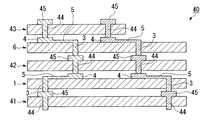
図3は、図1に示した接続用中間チップ1を備えた半導体装置の一例を示す図であって、図3中符号40は半導体装置である。この半導体装置40は、第1の半導体チップ41と、接続用中間チップ1と、第2の半導体チップ42と、接続用中間チップ6と、第3の半導体チップ43とをこの順に積層した構造となっている。
第1の半導体チップ41、第2の半導体チップ42、第3の半導体チップ43は、いずれも、素子部や回路部(図示せず)とは別に、三次元実装用の接続部材として、貫通電極44とポスト電極45とを接続用電極として形成したものである。すなわち、これら半導体チップ41、42、43は、素子部や回路部を形成した基板の能動面側にポスト電極45を形成し、このポスト電極45に導通する貫通電極44を、能動面と反対の側の面(裏面)に突出させてなるものである。なお、本例の半導体装置40では、第1の半導体チップ41と第2の半導体チップ42とはその基板形状が同じに形成されており、第3の半導体チップ43はこれらより基板形状が小さく形成されている。Next, a semiconductor device of the present invention using such connecting
FIG. 3 is a diagram showing an example of a semiconductor device provided with the connecting
Each of the
一方、接続用中間チップ1は図1に示した構造のものであり、接続用中間チップ6は、接続用中間チップ1に対して貫通電極3、ポスト電極4、配線部5の位置を変更しただけのものである。
そして、これらこれら半導体チップ41、42、43と接続用中間チップ1、6とは、半導体チップ側のポスト電極45と接続用中間チップ1、6側の貫通電極3とが例えば鉛フリーのはんだ(図示せず)によって接続し、また、半導体チップ側の貫通電極44と接続用中間チップ1、6側のポスト電極4とが例えば鉛フリーのはんだ(図示せず)によって接続することにより、積層されたものとなっている。On the other hand, the connecting
These semiconductor chips 41, 42, 43 and connecting
このような構成のもとに、接続用中間チップ1、6を介して各半導体チップ41、42、43を順次積層したことにより、平面視した状態で異なる位置に形成された各貫通電極3およびポスト電極4の位置を、再配置配線することができる。そして、本例では、特に異なる大きさの異種チップである第2の半導体チップ42と第3の半導体チップ43とを接続用中間チップ6によって積層させているため、三次元実装された半導体装置40の構造上の自由度を高めることができ、したがって、例えば半導体装置40の多機能化などの特性向上を図ることができる。 Under such a configuration, the semiconductor chips 41, 42, 43 are sequentially stacked via the connecting
なお、本例においては、各半導体チップ41、42、43を形成する基板と、接続用中間チップ1、6を形成する基板とをいずれもシリコン基板としている。このような構成により、接続用中間チップ1、6の熱膨張率が半導体チップ41、42、43の熱膨張率と同じとなり、したがって、接続用中間チップ1、6と半導体チップ41、42、43との間での、熱膨張率差に起因する電極間の接続部(はんだ)の剥離などを防止することができる。
また、特に第1の半導体チップ41および第2の半導体チップ42を形成する基板と、接続用中間チップ1、6を形成する基板とをいずれも同じ厚さでかつ同じ形状の基板としている。これにより、基板の共通化を可能にして製造コストの低減化を図ることができる。また、チップの厚さをほぼ標準化できることから、これらが積層されてなる半導体装置40の高さが、積層されたチップの数によってほぼ決まるようになる。したがって、この半導体装置40を搭載する機器の収納空間の設計を、例えばチップの厚さの倍数に標準化することができる。In this example, the substrate on which the semiconductor chips 41, 42, 43 are formed and the substrate on which the connecting
In particular, the substrate on which the
図4は、図1に示した接続用中間チップ1を備えた半導体装置の他の例を示す図であって、図4中符号50は半導体装置である。この半導体装置50は、第4の半導体チップ51と、接続用中間チップ7と、第5の半導体チップ52と、接続用中間チップ8および接続用中間チップ6と、第6の半導体チップ53とをこの順に積層した構造となっている。
本例の半導体装置50では、特に第5の半導体チップ52と第6の半導体チップ53との間において、第5の半導体チップ52における一つのポスト電極54aの位置と、第6の半導体チップ53における一つの貫通電極55aの位置とが平面視した状態でほぼ同じ箇所にあり、かつ、これらを互いに接続しない場合に適用される構造となっている。FIG. 4 is a view showing another example of the semiconductor device provided with the connecting
In the
すなわち、一つの接続中間チップを用いて第5の半導体チップ52と第6の半導体チップ53とを積層しようとした場合に、この接続中間チップでは、第5の半導体チップ52のポスト電極54aに接続させるための貫通電極と第6の半導体チップ53の貫通電極55aに接続させるためのポスト電極とが同じ位置に設けられることになり、したがってこれらの間が短絡してしまう。そこで、接続中間チップとして接続用中間チップ8と接続用中間チップ6とを積層して用いることにより、このような短絡を防止して各電極間の再配置配線を可能にしているのである。
このように複数(二つ)の接続用中間チップ8、6を組み合わせることにより、一つの接続用中間チップでは対応できないような複雑な再配置配線も可能になり、したがって再配置の自由度を格段に高めることができる。That is, when the
By combining a plurality of (two) connecting
図5は、図2に示した接続用中間チップ30を備えた半導体装置の一例を示す図であって、図5中符号60は半導体装置である。この半導体装置60は、第7の半導体チップ61と、前記接続用中間チップ30と、第8の半導体チップ62および第9の半導体チップ63とをこの順に積層した構造となっている。
本例の半導体装置50では、第7の半導体チップ61に対して第8の半導体チップ62および第9の半導体チップ63を異種チップとし、第8、第9の半導体チップ62、63については共に接続用中間チップ30上に積層するようにしている。そして、第7の半導体チップ61における一つのポスト電極65aを、第8、第9の半導体チップ62、63における各貫通電極64a、64aに導通させるようにしている。FIG. 5 is a view showing an example of a semiconductor device provided with the connecting
In the
すなわち、本例の半導体装置60では、前記接続用中間チップ30を用いることにより、平面視した状態で交差してしまうような再配置配線を可能にしている。したがって、図3、図4に示した接続用中間チップ1、6、7、8のような単層構造のものでは困難となる複雑な再配置配線を、複数積層することなく一つの接続用中間チップ30で再配置配線することができ、これにより再配置の自由度を格段に高めることができる。
なお、半導体装置とは、これまでに示してきた積層した半導体チップを、ひとつのパッケージとしてモジュール化したものも当然含むものである。In other words, in the
Note that the semiconductor device naturally includes one obtained by modularizing the stacked semiconductor chips described so far as one package.
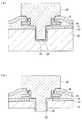
次に、このような構成からなる半導体装置40、50、60における、各半導体チップの貫通電極およびポスト電極の構造を、その製造方法に基づいて説明する。
まず、貫通電極およびポスト電極を形成する前の、半導体チップの構成について説明する。図6(a)において、図示しないトランジスタ、メモリ素子、その他の電子素子からなる集積回路が形成されたシリコン基板10の表面には、絶縁膜12が形成されている。この絶縁膜12は、例えば基板10の材料であるSi(シリコン)の酸化膜(SiO2)で形成されている。Next, the structure of the through electrode and the post electrode of each semiconductor chip in the
First, the configuration of the semiconductor chip before the through electrode and the post electrode are formed will be described. In FIG. 6A, an insulating
絶縁膜12上には、硼燐珪酸ガラス(以下、BPSGという)からなる層間絶縁膜14が形成されており、層間絶縁膜14上には、図示しない箇所で基板10に形成された集積回路と電気的に接続された電極としての電極パッド16が形成されている。この電極パッド16は、例えばTi(チタン)からなる第1層16a、TiN(窒化チタン)からなる第2層16b、AlCu(アルミニウム/銅)からなる第3層16c、及びTiNからなる第4層(キャップ層)16dが順に積層されて形成されている。 On the insulating
電極パッド16は、例えばスパッタリングによって第1層16a〜第4層16dからなる積層構造が層間絶縁膜14上の全面に形成され、レジスト等を用いて所定の形状(例えば、円形形状)にパターニングされることにより、形成されたものである。なお、本例では、電極パッド16が前記の積層構造により形成されている場合を例に挙げて説明するが、電極パッド16がAlのみで形成されていてもよい。ただし、電気抵抗の低い銅を用いて形成するのが好ましいのはもちろんである。また、電極パッド16は、前記の構成に限られず、必要とされる電気的特性、物理的特性、及び化学的特性に応じて適宜変更してもよい。なお、電極パッド16の下方には電子回路が形成されない構造となっている。 The
また、層間絶縁膜14上には電極パッド16を覆うように、絶縁層としてのパッシベーション膜18が形成されている。このパッシベーション膜18は、SiO2(酸化珪素)、SiN(窒化珪素)、ポリイミド樹脂等により形成することができる。 A
パッシベーション膜18については、SiO2若しくはSiNで形成される。また、パッシベーション膜18の膜厚としては、0.5μm程度以上とするのが好ましい。The
次に、以上の構成の半導体チップに対して、貫通電極およびポスト電極を形成するための各工程を順次説明する。まず、スピンコート法、ディッピング法、スプレーコート法等の方法によりレジスト(図示省略)をパッシベーション膜18上の全面に塗布する。なお、このレジストは、電極パッド16上を覆っているパッシベーション膜18を開口するために用いるものであり、フォトレジスト、電子線レジスト、X線レジストの何れであってもよく、ポジ型又はネガ型の何れであってもよい。 Next, each process for forming a penetration electrode and a post electrode with respect to the semiconductor chip having the above configuration will be sequentially described. First, a resist (not shown) is applied on the entire surface of the
パッシベーション膜18上にレジストを塗布したら、これのプリベークを行った後、所定のパターンが形成されたマスクを用いて露光処理及び現像処理を行い、レジストを所定形状にパターニングする。なお、レジストの形状は、電極パッド16の開口形状及び基板10に形成する孔の断面形状に応じて設定される。レジストのパターニングが終了したら、ポストベークを行った後、図6(b)に示すように、電極パッド16を覆うパッシベーション膜18の一部をエッチングして開口部H1を形成する。図6(b)は、パッシベーション膜18を開口して開口部H1を形成した状態を示す断面図である。 When a resist is applied on the
なお、エッチングにはドライエッチングが好適に用いられ、具体的には、反応性イオンエッチング(RIE:Reactive Ion Etching)が好適に用いられる。ただし、エッチングとしてウェットエッチングを用いることもできる。その開口サイズは、次工程で電極パッド16に形成される開口の径及び基板10に形成される孔の径より大きく、パッドサイズより小さいサイズ、例えば90μm程度に設定される。その後、レジストを、剥離液あるいはアッシング等により除去する。なお、ここまでの工程は、従来の半導体チップの加工と何ら異なるところはない。 Note that dry etching is preferably used for etching, and specifically, reactive ion etching (RIE) is preferably used. However, wet etching can also be used as etching. The opening size is set to be larger than the diameter of the opening formed in the
以上の工程が終了したら、電極パッド16と、その下の層間絶縁膜14および絶縁膜12に開口部H2を形成する。これにより基板10の一部を露出させる。この開口はレジストを用い、前述と同様のフォトリソプロセスで所望のサイズに開口する。図6(c)は電極パッドおよび層間絶縁膜14、絶縁膜12を開口して、基板10の一部を露出させた状態を示す断面図である。なおH2の開口径は、H1より小さく、次工程で開口するプラグ When the above steps are completed, an opening H2 is formed in the
次に、基板全面にドライエッチング時のマスクとなるエッチングマスク19を形成する。この材料としては、SiO2もしくはSiNで形成する。あるいはこれらの積層膜でも良い。この膜厚としては、基板に穿孔する穴の深さを実現できるに足る選択比から算出するが、2μm以上とするのが望ましい。2μm以上とするのは、前述の選択比を確保する上で必要であるからである。このエッチングマスクの開口はレジストを用い、前述と同様のフォトリソプロセスでパターン形成を行う。図7(a)はエッチングマスクを所定の大きさに開口した状態を示す断面図である。その径は、プラグ径と同程度、例えば30μm程度に設定される。Next, an
このエッチングマスク19をマスクとして、ドライエッチングにより図7(b)に示すように、基板10を穿孔する。なお、ここでは、ドライエッチングとしてRIEのほかにICP(Inductively Coupled Plasma)を用いることもできる。図7(b)は、基板10を穿孔して、孔部H3を形成した状態を示す断面図である。なお、孔部H3の深さについては、最終的に形成する半導体チップの厚みに応じて適宜設定されるが、例えば深さ70μm程度とされる。Using this
また、図7(b)に示したように、基板10に孔部H3を形成すると、ドライエッチングによりエッチングマスク19は、穿孔時に緩やかにエッチングされ、孔部H3の形成終了時には、残膜がほとんどなくなっている。図7(b)以降は、パッシベーション18にエッチングマスクの残膜19を含め、エッチングマスクの残膜19を省略して図示している。 Further, as shown in FIG. 7B, when the hole H3 is formed in the
以上の工程が終了したら、次に、パッシベーション膜18上並びに孔部H3の内壁及び底面に、絶縁膜20を形成する。図7(c)は、電極パッド16の上方並びに孔部H3の内壁及び底面に絶縁膜20を形成した状態を示す断面図である。
この絶縁膜20は、電流リークの発生、酸素及び水分等による基板10の浸食等を防止するために設けられ、PECVD(Plasma Enhanced Chemical Vapor Deposition)を用いて形成したテトラエトキシシラン(以下、TEOSという)、すなわちPE−TEOSによって形成される。この絶縁膜20の厚みとしては、例えば2μmとされる。なお、絶縁膜20としては、PE−TEOSに代えて、オゾンCVDを用いて形成したTEOS(O3−TEOS)、又はCVDを用いて形成した酸化シリコンを用いることもできる。After the above steps are completed, an insulating
The insulating
続いて、スピンコート法、ディッピング法、スプレーコート法等の方法によりレジスト(図示せず)をパッシベーション膜18上の全面に塗布する。あるいは、ドライフィルムレジストを用いても良い。なお、このレジストは、電極パッド16の一部の上方を開口するために用いるものであり、フォトレジスト、電子線レジスト、X線レジストの何れであってもよく、ポジ型又はネガ型の何れであってもよい。 Subsequently, a resist (not shown) is applied on the entire surface of the
パッシベーション膜18上にレジストを塗布したら、これのプリベークを行った後、所定のパターンが形成されたマスクを用いて露光処理及び現像処理を行い、電極パッド16の表面の一部のみが露出されるようにレジストが残された形状、例えば孔部H2を中心とした円環形状にレジストをパターニングする。
レジストのパターニングが終了したら、ポストベークを行った後、エッチングで電極パッド16の一部を覆う絶縁膜20を除去し、電極パッド16の一部を開口する。なお、エッチングにはドライエッチングを用いるのが好ましく、特に反応性イオンエッチングを用いるのが好ましい。また、エッチングとしてウェットエッチングを用いることもできる。なお、このとき、電極パッド16を構成する第4層16dも併せて除去する。When a resist is applied on the
After the resist patterning is completed, post-baking is performed, and then the insulating
図8(a)は、電極パッド16を覆う絶縁膜20の一部を除去した状態を示す断面図である。図8(a)に示すように、電極パッド16の上方は、外径が80μm程度、内径が70μm程度の円環状の開口部H4となり、電極パッド16の一部が露出した状態となる。この開口部H4によって、後の工程で形成される接続端子(電極部)と電極パッド16とを接続することができる。したがって、開口部H4は電極パッド16上であれば、孔部H3が形成された部位以外の箇所に形成されていればよく、隣接していてもよい。 FIG. 8A is a cross-sectional view showing a state where a part of the insulating
本例では、電極パッド16のほぼ中央に孔部H3を形成する場合を例に挙げている。よって、開口部H4は、この孔部H3を取り囲むように、つまり電極パッド16の露出面積を大きくするのが、電極パッド16と後に形成される接続端子との接続抵抗を小さくする上で好ましい。また、孔部H3の形成場所は電極パッドのほぼ中央でなくてもよく、複数の孔が形成されていてもよい。なお、電極パッド16を覆う絶縁膜20の一部を除去して電極パッド16の一部を露出させたら、除去する際に用いたレジストを剥離液によって除去する。 In this example, the case where the hole H3 is formed in the approximate center of the
以上の工程が終了したら、電極パッド16の露出部並びに孔部H3の内壁及び底部に下地膜22を形成する。ここで、下地膜22は、バリア層及びシード層からなり、まずバリア層を形成した後で、バリア層上にシード層を形成することで成膜される。ここで、バリア層は例えばTiおよびTiNによって形成され、シード層はCuによって形成される。これらは、例えばIMP(イオンメタルプラズマ)法、又は、真空蒸着、スパッタリング、イオンプレーティング等のPVD(Phisical Vapor Deposition)法で形成される。なお、バリア層及びシード層は本段階ではウェハ全面に形成し、最後に不要部をエッチングで除去する。 When the above steps are completed, the
図8(b)は、下地膜22を形成した状態を示す断面図である。下地膜22を構成するバリア層の膜厚は、例えば0.1μm程度とされ、シード層の膜厚は、例えば0.3μm程度とされる。なお、ここでいう不要部とは、例えば電極パッドを除くパッシベーション膜18上に形成されているバリア層及びシード層を指す。 FIG. 8B is a cross-sectional view showing a state in which the
下地膜22の形成を終了したら、次に、接続端子を形成する領域を内径120μmで露出させ、それ以外にレジストが形成されるようにパターニングを行う。レジストによるパターニング工程は従前のプロセスと全く同じである。ここで用いるレジストは、次に行うメッキに対する耐性が高いものを使用し、また膜厚も、ポスト電極の高さ以上に形成しておく。次に、電気化学プレーティング(ECP)法を用いて、孔部H3の内部及び電極パッド16上にメッキ処理を施して、孔部H3内部を銅で埋め込むとともに、電極パッド16上に突出した形状の、金属層としてのポスト電極24を高さ10μm程度となるように形成する。このようにして、電極パッド16の上方に電極パッド16と電気的に接続され、かつ基板10の表面側の外部電極となる、前述の半導体チップにおけるポスト電極24が形成される。なお、このポスト電極24上には、はんだとして鉛フリーのもの、例えばSnAg(図示せず)を形成しておく。 After the formation of the
次いで、レジストを剥離し、バリア層及びシード層の不要部(図示省略)をエッチングによって除去することにより、図9(a)に示すような状態が形成される。なお、シード層のエッチングはウェット方式でエッチング液によりエッチングする方法が一般的である。また、バリア層はウェット方式でもよいが、RIE等によるドライエッチングでもよい。この際、ポスト電極24がエッチングされるのを防ぐため、ポスト電極24を囲むようにレジストを形成した後、エッチングを行ってもよい。 Next, the resist is removed, and unnecessary portions (not shown) of the barrier layer and the seed layer are removed by etching, thereby forming a state as shown in FIG. The seed layer is generally etched by a wet method using an etchant. The barrier layer may be a wet method, but may be dry etching such as RIE. At this time, in order to prevent the
その後、例えば孔部H3に埋め込んだ銅(貫通電極)が基板の裏面に露出するまで基板10の裏面を例えば基板10の厚さが50μm程度となるまで薄膜化し、これによってポスト電極24に連続した貫通電極部分を基板10の裏面から突出させる。この薄膜化には、機械的研磨または化学的なエッチング、ウェットあるいはドライエッチングが単独で採用され、あるいは併用される。さらに、基板10の裏面から突出した金属部分の端面の、絶縁層20と下地層22とを機械的研磨、ウェットあるいはドライエッチング等によって除去し、これによって図9(b)に示すようにポスト電極24と電気的に接続された貫通電極26を形成する。
そして、ダイシングによって個片化することにより、ポスト電極24と貫通電極26とを有した各半導体チップを得る。Thereafter, for example, the back surface of the
Then, each semiconductor chip having the
次に、前記半導体装置40、50、60における、接続用中間チップの貫通電極およびポスト電極の構造を、その製造方法に基づいて説明する。なお、本例では、特に図1に示したような単層構造の接続用中間チップについて説明する。
まず、図10(a)に示すようにシリコンからなる基板70を用意する。ここで、この基板70は、前述のシリコン基板10とは異なり、各種素子からなる集積回路を形成していないものである。したがって、この接続用中間チップの製造は、前記半導体チップとは全く別に形成されることから、この接続用中間チップの歩留まりが半導体チップの歩留まりに影響を及ぼすことはない。Next, the structure of the through electrode and the post electrode of the connecting intermediate chip in the
First, as shown in FIG. 10A, a
このような基板70を用意したら、これの表面側に表面あるいは両面、側面に熱酸化膜、またはプラズマTEOSなどによるSiO2からなる酸化膜71を、厚さ1μm程度に形成する。続いて、この酸化膜71上の所定位置に、再配置配線となる導電パターン72を形成する。この導電パターン72としては、例えばTi(チタン)からなる第1層と、TiN(窒化チタン)からなる第2層と、Alからなる第3層とを順に積層することで導電層を形成し、さらにこの導電層を所望形状にパターニングすることで形成する。Once you have such a
次いで、この導電パターン72を覆ってSiO2またはSiNからなるパッシベーション膜73を形成し、さらにこれをパターニングしてポストおよび貫通電極を形成する領域のパッシベーション膜開口する。
図10(a)は、パッシベーション膜を2ヶ所開口した状態を示す断面図である。なお、パッシベーション膜は、必ずしも必要ではなく、そのまま次工程に進んでも良い。Next, a
FIG. 10A is a cross-sectional view showing a state in which two passivation films are opened. Note that the passivation film is not necessarily required, and may proceed to the next process as it is.
次に、パッシベーション上にレジスト(図示せず)を形成し、パッシベーションの開口部より小さい径、例えば60μmに導電パターン72を、さらにはその下の絶縁膜71をドライエッチングにより開口する。これにより開口部H6が形成できる。
続いて、剥離液によりレジストを剥離後、プラズマTEOS法等により、エッチングマスク用のSiO2からなる酸化膜74を堆積する。
このエッチングマスク上に再びレジスト(図示せず)を形成し、フォト、エッチングプロセスにより、開口部H6より内側に貫通電極と同等の径の開口部H7を形成する。この後、剥離液によりレジストを剥離する。
図10(b)は、導電パターン72および絶縁膜71を開口し、そののちエッチングマスク用のSiO2からなる酸化膜74を堆積、開口部H7を形成した状態の断面図を図示したものである。Next, a resist (not shown) is formed on the passivation, and the
Subsequently, after removing the resist with a stripping solution, an
A resist (not shown) is formed again on the etching mask, and an opening H7 having the same diameter as the through electrode is formed inside the opening H6 by a photo and etching process. Thereafter, the resist is stripped with a stripping solution.
FIG. 10B illustrates a cross-sectional view of a state in which the
そして、このエッチングマスク74をマスクにしてRIE等のドライエッチングを行い、基板70を穿孔して孔部H8を形成する。
なお、ここでは、ドライエッチングとしてRIEのほかにICP(Inductively Coupled Plasma)を用いることもできる。図11(a)は、基板10を穿孔して、孔部H3を形成した状態を示す断面図である。なお、孔部H8の深さについては、最終的に形成する半導体チップの厚みに応じて適宜設定されるが、例えば深さ70μm程度とされる。
この時点では、エッチングマスク74は、穿孔時に緩やかにエッチングされ、孔部H8の形成終了時には、残膜がほとんどなくなっている。Then, dry etching such as RIE is performed using the
Here, in addition to RIE, ICP (Inductively Coupled Plasma) can also be used as dry etching. FIG. 11A is a cross-sectional view showing a state in which the
At this point, the
次いで、酸化膜74上並びに孔部H8の内壁面及び底面に、図11(b)に示すようにSiO2又はSiNあるいはそれらの積層膜からなる絶縁膜75を形成する。
この絶縁膜20は、電流リークの発生、酸素及び水分等による基板10の浸食等を防止するために設けられ、PECVD(Plasma Enhanced Chemical Vapor Deposition)を用いて形成したテトラエトキシシラン(以下、TEOSという)、すなわちPE−TEOSによって形成される。この絶縁膜20の厚みとしては、例えば2μmとされる。なお、絶縁膜20としては、PE−TEOSに代えて、オゾンCVDを用いて形成したTEOS(O3−TEOS)、又はCVDを用いて形成した酸化シリコンを用いることもできる。Next, as shown in FIG. 11B, an insulating
The insulating
続いて、レジスト層(図示せず)を形成し、さらにマスクを用いてこれを露光・現像することにより、所望パターン形状にする。そして、この所望パターン形状のレジストをマスクとして絶縁膜75をエッチングすることにより、図12(a)に示すように、孔H8の周囲に円環状の開口部H79を形成するとともに、ポスト電極形成箇所に開口部H10を形成する。これら開口部H9、H10については、いずれもドライエッチングによりその底部に導電パターン72が露出するように形成する。この後、レジストを剥離液によって剥離する。 Subsequently, a resist layer (not shown) is formed, and this is exposed and developed using a mask to obtain a desired pattern shape. Then, by etching the insulating
次いで、図12(b)に示すように、導電パターン72の露出部(開口部H9、H10の内壁を含む)並びに孔部H8、の内壁及び底部に下地膜76を形成する。ここで、下地膜76は前記下地膜22と同様に、バリア層及びシード層からなるものであり、バリア層としては例えばTiおよびTiNが、またシード層としてはCuが用いられている。これらは、例えばIMP(イオンメタルプラズマ)法、又は、真空蒸着、スパッタリング、イオンプレーティング等のPVD(Phisical Vapor Deposition)法で形成される。なお、バリア層及びシード層は本段階ではウェハ全面に形成し、最後に不要部をエッチングで除去する。 Next, as shown in FIG. 12B, a
次いで、開口部H9に囲まれた部分と開口部H10とを露出させるようにしてレジストパターンを形成し、さらに電気化学プレーティング(ECP)法を用いて、孔部H6の内部及び開口部7内にメッキ処理を施す。ここで用いるレジストは、メッキに対する耐性が高いものを使用し、また膜厚も、ポスト電極の高さ以上に形成しておく。これにより、図13(a)に示すように孔部H8内部を銅で埋め込むとともに、開口部H9内の導電パターン72上にも銅を埋め込む。また、これと同時に、開口部H10内の導電パターン72上にも銅を埋め込み、ポスト電極を形成する。ここで、孔部H8内および開口部H9内への埋め込みと、開口部H10内への埋め込みとは別工程で行ってもよく、その場合、孔部H8内および開口部H9内への埋め込みには埋め込み性の良いメッキ材料を用い、開口部H10内への埋め込みにはレベリング性の良いメッキ材料を用いるのが好ましい。 Next, a resist pattern is formed so as to expose the portion surrounded by the opening H9 and the opening H10, and further, using the electrochemical plating (ECP) method, the inside of the hole H6 and the inside of the
このようにして孔部H8内および開口部H9内に埋め込まれた銅により、貫通電極77が形成され、また、開口部H10内に埋め込まれた銅により、ポスト電極8が形成される。さらに、これら貫通電極77とポスト電極78との間を接続する導電パターン72が、配線部79となる。なお、ポスト電極78上には、はんだとして鉛フリーのもの、例えばSnAg(図示せず)を形成しておく。 Thus, the through electrode 77 is formed by the copper buried in the hole H8 and the opening H9, and the post electrode 8 is formed by the copper buried in the opening H10. Further, the
次いで、レジストを剥離し、下地層76(バリア層及びシード層)の不要部(図示省略)をエッチングにより除去する。なお、シード層のエッチングはウェット方式でエッチング液によりエッチングする方法が一般的である。また、バリア層はウェット方式でもよいが、RIE等によるドライエッチングでもよい。この際、ポスト電極78がエッチングされるのを防ぐため、ポスト電極24を囲むようにレジストを形成した後、エッチングを行ってもよい。
その後、例えば貫通電極77が基板の裏面に露出するまで基板70の裏面を薄膜化し、これによってその突出部を形成する。この薄膜化には、機械的研磨または化学的なエッチングが単独で採用され、あるいは併用される。さらに、図13(b)に示すように基板70の裏面から突出した金属部分の端面の、絶縁層75と下地層76とを機械的研磨、あるいはエッチング等によって除去し、これによってポスト電極78に電気的に接続された貫通電極77を得る。
そして、ダイシングによって個片化することにより、貫通電極77とポスト電極78とこれらの間を導通させる配線部79とを有した、接続用中間チップを得る。
このようにして作製した半導体チップならびに中間チップを積層して、貫通電極の先端部と、ポスト電極の表面を接合することにより、図3や図4に示された、中間チップと半導体チップが積層された半導体装置を得ることができる。Next, the resist is peeled off, and unnecessary portions (not shown) of the base layer 76 (barrier layer and seed layer) are removed by etching. The seed layer is generally etched by a wet method using an etchant. The barrier layer may be a wet method, but may be dry etching such as RIE. At this time, in order to prevent the
Thereafter, for example, the back surface of the
Then, by dividing into pieces by dicing, an intermediate chip for connection having a through electrode 77, a
By stacking the semiconductor chip and the intermediate chip thus manufactured and joining the tip of the through electrode and the surface of the post electrode, the intermediate chip and the semiconductor chip shown in FIGS. 3 and 4 are stacked. The obtained semiconductor device can be obtained.
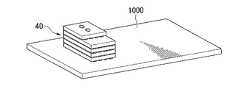
次に、前記の半導体装置40を備えた回路基板及び電子機器の例について説明する。
図14は本発明の回路基板の一実施形態の概略構成を示す斜視図である。図14に示すようにこの実施形態の回路基板1000には、前記の半導体装置40が搭載されている。
なお、半導体装置40は、積層後パッケージ化されたものを実装するのが一般的であるが、積層した半導体装置をそのまま実装してもよい。図14においては、回路基板上に実装された形態がわかりやすいように、パッケージを省略し、前記半導体装置をそのまま示している。
回路基板1000は、例えばガラスエポキシ基板等の有機系基板からなるもので、例えば銅等からなる配線パターン(図示せず)が所望の回路となるように形成され、さらにこれら配線パターンに電極パッド(図示せず)が接続されている。そして、この電気パッドに半導体装置40における前記第1の半導体チップ41の貫通電極44が、パッケージ化する際に一次実装された基板を介して、電気的に接続されることにより、半導体装置40は回路基板1000上に実装されたものとなっている。
このような構成の回路基板1000にあっては、実装密度が高く、しかも再配置配線がなされた半導体装置40を備えていることから、小型化、軽量化が図られたものとなり、また配線接続の信頼性も高いものとなる。Next, an example of a circuit board and electronic equipment provided with the
FIG. 14 is a perspective view showing a schematic configuration of an embodiment of a circuit board of the present invention. As shown in FIG. 14, the
The
The
In the
図15は本発明の電子機器の一実施形態としての、携帯電話の概略構成を示す斜視図である。図15に示すようにこの携帯電話300は、前記の半導体装置40又は前記回路基板1000を、その筐体内部に配設したものである。
このような構成の携帯電話300(電子機器)にあっても、実装密度が高く再配置配線がなされた半導体装置2を備えていることから、小型化、軽量化が図られたものとなり、また配線接続の信頼性も高いものとなる。FIG. 15 is a perspective view showing a schematic configuration of a mobile phone as an embodiment of the electronic apparatus of the present invention. As shown in FIG. 15, the
Even in the mobile phone 300 (electronic device) having such a configuration, the semiconductor device 2 having a high mounting density and a rearranged wiring is provided, so that the size and weight can be reduced. The reliability of wiring connection is also high.
なお、電子機器としては、前記の携帯電話に限られることなく、種々の電子機器に適用することができる。例えば、ノート型コンピュータ、液晶プロジェクタ、マルチメディア対応のパーソナルコンピュータ(PC)及びエンジニアリング・ワークステーション(EWS)、ページャ、ワードプロセッサ、テレビ、ビューファインダ型又はモニタ直視型のビデオテープレコーダ、電子手帳、電子卓上計算機、カーナビゲーション装置、POS端末、タッチパネルを備えた装置等の電子機器に適用することができる。 Note that the electronic device is not limited to the mobile phone described above, and can be applied to various electronic devices. For example, notebook computers, liquid crystal projectors, multimedia-compatible personal computers (PCs) and engineering workstations (EWS), pagers, word processors, televisions, viewfinder type or monitor direct view type video tape recorders, electronic notebooks, electronic desks The present invention can be applied to electronic devices such as a computer, a car navigation device, a POS terminal, and a device having a touch panel.
1、6、7、8、30…接続用中間チップ、2、31…基板、3、32…貫通電極、
3a、32a…突出部、4、34、34a…ポスト電極、5、33…配線部、
40、50、60…半導体装置、41…第1の半導体チップ、
42…第2の半導体チップ、43…第3の半導体チップ、44…貫通電極、
45…ポスト電極、51…第4の半導体チップ、52…第5の半導体チップ、
53…第6の半導体チップ、54、54a…貫通電極、55、55a…ポスト電極、
61…第7の半導体チップ、62…第8の半導体チップ、63…第9の半導体チップ、
64…貫通電極、65、65a…ポスト電極
1, 6, 7, 8, 30 ... intermediate chip for connection, 2, 31 ... substrate, 3, 32 ... through electrode,
3a, 32a ... projecting part, 4, 34, 34a ... post electrode, 5, 33 ... wiring part,
40, 50, 60 ... semiconductor device, 41 ... first semiconductor chip,
42 ... 2nd semiconductor chip, 43 ... 3rd semiconductor chip, 44 ... Through-hole electrode,
45 ... Post electrode, 51 ... Fourth semiconductor chip, 52 ... Fifth semiconductor chip,
53 ... Sixth semiconductor chip, 54, 54a ... Through electrode, 55, 55a ... Post electrode,
61 ... seventh semiconductor chip, 62 ... eighth semiconductor chip, 63 ... ninth semiconductor chip,
64 ... through electrode, 65, 65a ... post electrode
Claims (11)
Translated fromJapanese前記接続用中間チップは、基板と、該基板の表裏面のうちの少なくとも一方の面側に突出する貫通電極と、基板の他方の面側において、平面視した状態で前記貫通電極とは異なる位置に配置されたポスト電極と、基板中または基板面に配置されて前記貫通電極とポスト電極とを導通させる配線部と、を備えてなり、The connecting intermediate chip has a position different from that of the through-electrode in a plan view on a substrate, a through-electrode protruding to at least one of the front and back surfaces of the substrate, and the other surface of the substrate. A post electrode disposed in the substrate, and a wiring portion disposed in the substrate or on the substrate surface and electrically connecting the through electrode and the post electrode,
前記接続用中間チップの一方の面側に、前記第1の半導体チップがその接続用電極を接続用中間チップの貫通電極に導通した状態で接続され、The first semiconductor chip is connected to one surface side of the connection intermediate chip in a state where the connection electrode is electrically connected to the through electrode of the connection intermediate chip,
前記接続用中間チップの他方の面側に、前記第2の半導体チップがその接続用電極を接続用中間チップのポスト電極に導通した状態で接続され、The second semiconductor chip is connected to the other surface side of the connecting intermediate chip in a state where the connecting electrode is electrically connected to the post electrode of the connecting intermediate chip,
第1の半導体チップと第2の半導体チップとは互いに異なる大きさの異種のチップであることを特徴とする半導体装置。A semiconductor device, wherein the first semiconductor chip and the second semiconductor chip are different types of chips having different sizes.
Priority Applications (5)
| Application Number | Priority Date | Filing Date | Title |
|---|---|---|---|
| JP2003335675AJP4238685B2 (en) | 2003-09-26 | 2003-09-26 | Semiconductor devices, circuit boards, electronic equipment |
| TW093128616ATWI251313B (en) | 2003-09-26 | 2004-09-21 | Intermediate chip module, semiconductor device, circuit board, and electronic device |
| US10/947,607US7193308B2 (en) | 2003-09-26 | 2004-09-22 | Intermediate chip module, semiconductor device, circuit board, and electronic device |
| CNB2004100798573ACN100440488C (en) | 2003-09-26 | 2004-09-23 | Intermediate chip modules, semiconductor devices, circuit boards, electronic equipment |
| KR1020040076551AKR100687980B1 (en) | 2003-09-26 | 2004-09-23 | Semiconductor devices, circuit boards and electronics |
Applications Claiming Priority (1)
| Application Number | Priority Date | Filing Date | Title |
|---|---|---|---|
| JP2003335675AJP4238685B2 (en) | 2003-09-26 | 2003-09-26 | Semiconductor devices, circuit boards, electronic equipment |
Publications (2)
| Publication Number | Publication Date |
|---|---|
| JP2005101460A JP2005101460A (en) | 2005-04-14 |
| JP4238685B2true JP4238685B2 (en) | 2009-03-18 |
Family
ID=34463000
Family Applications (1)
| Application Number | Title | Priority Date | Filing Date |
|---|---|---|---|
| JP2003335675AExpired - LifetimeJP4238685B2 (en) | 2003-09-26 | 2003-09-26 | Semiconductor devices, circuit boards, electronic equipment |
Country Status (1)
| Country | Link |
|---|---|
| JP (1) | JP4238685B2 (en) |
- 2003
- 2003-09-26JPJP2003335675Apatent/JP4238685B2/ennot_activeExpired - Lifetime
Also Published As
| Publication number | Publication date |
|---|---|
| JP2005101460A (en) | 2005-04-14 |
Similar Documents
| Publication | Publication Date | Title |
|---|---|---|
| US7193308B2 (en) | Intermediate chip module, semiconductor device, circuit board, and electronic device | |
| JP3972846B2 (en) | Manufacturing method of semiconductor device | |
| JP3821125B2 (en) | Semiconductor device manufacturing method, semiconductor device, circuit board, electronic device | |
| JP2004311948A (en) | Semiconductor device, semiconductor device, electronic device, and method of manufacturing semiconductor device | |
| US8409981B2 (en) | Semiconductor package with a metal post and manufacturing method thereof | |
| JP4289146B2 (en) | Manufacturing method of three-dimensional mounting type semiconductor device | |
| JP2006179752A (en) | Semiconductor device manufacturing method, semiconductor device, laminated semiconductor device, circuit board, and electronic apparatus | |
| CN101197298A (en) | Manufacturing method of semiconductor device and semiconductor device | |
| JP2011003645A (en) | Semiconductor device, and method of manufacturing the same | |
| JP4967340B2 (en) | SEMICONDUCTOR DEVICE, SEMICONDUCTOR DEVICE MANUFACTURING METHOD, AND ELECTRONIC DEVICE | |
| JP2006041148A (en) | Semiconductor device manufacturing method, semiconductor device, and electronic apparatus | |
| US20050179120A1 (en) | Process for producing semiconductor device, semiconductor device, circuit board and electronic equipment | |
| JP4114660B2 (en) | Semiconductor device manufacturing method, semiconductor device, circuit board, electronic device | |
| JP4735614B2 (en) | Circuit board | |
| JP2005150299A (en) | SEMICONDUCTOR CHIP, SEMICONDUCTOR DEVICE, SEMICONDUCTOR DEVICE MANUFACTURING METHOD, CIRCUIT BOARD, AND ELECTRONIC DEVICE | |
| JP4509486B2 (en) | Semiconductor device manufacturing method, semiconductor device, and electronic apparatus | |
| JP4238685B2 (en) | Semiconductor devices, circuit boards, electronic equipment | |
| JP4292748B2 (en) | Manufacturing method of semiconductor device | |
| JP2006049557A (en) | Semiconductor device | |
| JP4304905B2 (en) | Manufacturing method of semiconductor device | |
| JP2006041218A (en) | Semiconductor device manufacturing method, semiconductor device, and electronic apparatus | |
| JP4175241B2 (en) | Manufacturing method of semiconductor device | |
| JP2005150437A (en) | Intermediate chip module, semiconductor device, circuit board, and electronic device | |
| JP4033021B2 (en) | Semiconductor device and manufacturing method thereof | |
| JP4127095B2 (en) | Manufacturing method of semiconductor device |
Legal Events
| Date | Code | Title | Description |
|---|---|---|---|
| A621 | Written request for application examination | Free format text:JAPANESE INTERMEDIATE CODE: A621 Effective date:20050628 | |
| A521 | Request for written amendment filed | Free format text:JAPANESE INTERMEDIATE CODE: A821 Effective date:20050629 | |
| A131 | Notification of reasons for refusal | Free format text:JAPANESE INTERMEDIATE CODE: A131 Effective date:20080722 | |
| A521 | Request for written amendment filed | Free format text:JAPANESE INTERMEDIATE CODE: A523 Effective date:20080818 | |
| TRDD | Decision of grant or rejection written | ||
| A01 | Written decision to grant a patent or to grant a registration (utility model) | Free format text:JAPANESE INTERMEDIATE CODE: A01 Effective date:20081125 | |
| A01 | Written decision to grant a patent or to grant a registration (utility model) | Free format text:JAPANESE INTERMEDIATE CODE: A01 | |
| A61 | First payment of annual fees (during grant procedure) | Free format text:JAPANESE INTERMEDIATE CODE: A61 Effective date:20081208 | |
| FPAY | Renewal fee payment (event date is renewal date of database) | Free format text:PAYMENT UNTIL: 20120109 Year of fee payment:3 | |
| R150 | Certificate of patent or registration of utility model | Ref document number:4238685 Country of ref document:JP Free format text:JAPANESE INTERMEDIATE CODE: R150 Free format text:JAPANESE INTERMEDIATE CODE: R150 | |
| FPAY | Renewal fee payment (event date is renewal date of database) | Free format text:PAYMENT UNTIL: 20120109 Year of fee payment:3 | |
| FPAY | Renewal fee payment (event date is renewal date of database) | Free format text:PAYMENT UNTIL: 20130109 Year of fee payment:4 | |
| FPAY | Renewal fee payment (event date is renewal date of database) | Free format text:PAYMENT UNTIL: 20130109 Year of fee payment:4 | |
| FPAY | Renewal fee payment (event date is renewal date of database) | Free format text:PAYMENT UNTIL: 20140109 Year of fee payment:5 | |
| S531 | Written request for registration of change of domicile | Free format text:JAPANESE INTERMEDIATE CODE: R313531 | |
| R350 | Written notification of registration of transfer | Free format text:JAPANESE INTERMEDIATE CODE: R350 | |
| S111 | Request for change of ownership or part of ownership | Free format text:JAPANESE INTERMEDIATE CODE: R313113 | |
| R360 | Written notification for declining of transfer of rights | Free format text:JAPANESE INTERMEDIATE CODE: R360 | |
| R360 | Written notification for declining of transfer of rights | Free format text:JAPANESE INTERMEDIATE CODE: R360 | |
| R371 | Transfer withdrawn | Free format text:JAPANESE INTERMEDIATE CODE: R371 | |
| S111 | Request for change of ownership or part of ownership | Free format text:JAPANESE INTERMEDIATE CODE: R313113 | |
| R350 | Written notification of registration of transfer | Free format text:JAPANESE INTERMEDIATE CODE: R350 | |
| R250 | Receipt of annual fees | Free format text:JAPANESE INTERMEDIATE CODE: R250 | |
| R250 | Receipt of annual fees | Free format text:JAPANESE INTERMEDIATE CODE: R250 | |
| R250 | Receipt of annual fees | Free format text:JAPANESE INTERMEDIATE CODE: R250 | |
| R250 | Receipt of annual fees | Free format text:JAPANESE INTERMEDIATE CODE: R250 | |
| R250 | Receipt of annual fees | Free format text:JAPANESE INTERMEDIATE CODE: R250 | |
| EXPY | Cancellation because of completion of term |