JP4234737B2 - MEMS switch - Google Patents
MEMS switchDownload PDFInfo
- Publication number
- JP4234737B2 JP4234737B2JP2006201064AJP2006201064AJP4234737B2JP 4234737 B2JP4234737 B2JP 4234737B2JP 2006201064 AJP2006201064 AJP 2006201064AJP 2006201064 AJP2006201064 AJP 2006201064AJP 4234737 B2JP4234737 B2JP 4234737B2
- Authority
- JP
- Japan
- Prior art keywords
- electrode
- fixed
- insulating layer
- movable beam
- contact
- Prior art date
- Legal status (The legal status is an assumption and is not a legal conclusion. Google has not performed a legal analysis and makes no representation as to the accuracy of the status listed.)
- Expired - Fee Related
Links
Images


Classifications
- H—ELECTRICITY
- H01—ELECTRIC ELEMENTS
- H01H—ELECTRIC SWITCHES; RELAYS; SELECTORS; EMERGENCY PROTECTIVE DEVICES
- H01H59/00—Electrostatic relays; Electro-adhesion relays
- H01H59/0009—Electrostatic relays; Electro-adhesion relays making use of micromechanics
- H—ELECTRICITY
- H01—ELECTRIC ELEMENTS
- H01H—ELECTRIC SWITCHES; RELAYS; SELECTORS; EMERGENCY PROTECTIVE DEVICES
- H01H1/00—Contacts
- H01H1/50—Means for increasing contact pressure, preventing vibration of contacts, holding contacts together after engagement, or biasing contacts to the open position
- H—ELECTRICITY
- H01—ELECTRIC ELEMENTS
- H01H—ELECTRIC SWITCHES; RELAYS; SELECTORS; EMERGENCY PROTECTIVE DEVICES
- H01H1/00—Contacts
- H01H1/12—Contacts characterised by the manner in which co-operating contacts engage
- H01H1/14—Contacts characterised by the manner in which co-operating contacts engage by abutting
- H01H1/20—Bridging contacts
- H—ELECTRICITY
- H01—ELECTRIC ELEMENTS
- H01H—ELECTRIC SWITCHES; RELAYS; SELECTORS; EMERGENCY PROTECTIVE DEVICES
- H01H57/00—Electrostrictive relays; Piezoelectric relays
- H01H2057/006—Micromechanical piezoelectric relay
Landscapes
- Micromachines (AREA)
Description
Translated fromJapanese本発明は,高周波回路用スイッチとしても応用が可能なMEMS(Micro-Electro-Mechanical System)スイッチに関する。 The present invention relates to a MEMS (Micro-Electro-Mechanical System) switch that can be applied as a switch for a high-frequency circuit.
半導体プロセスを応用したMEMSは、広い範囲の応用が嘱望されている。例えば、高周波回路応用の分野においては、RFスイッチとしてのMEMSの応用が強く望まれている。 A wide range of applications of MEMS using semiconductor processes is desired. For example, in the field of high-frequency circuit applications, the application of MEMS as an RF switch is strongly desired.
高周波回路応用のMEMSスイッチとしては、直流(DC)回路から高周波回路まで使用可能であり、2個の接点がオーミック接触して通電するDCコンタクト型MEMSスイッチと、主として10GHz以上の高周波のみで使用可能であり、2個の接点が薄い誘電膜を介して接触するキャパシティブ型スイッチとに大別される。 The MEMS switch for high frequency circuit applications can be used from a direct current (DC) circuit to a high frequency circuit, and can be used only with a high frequency of 10 GHz or more, and a DC contact type MEMS switch in which two contacts are in ohmic contact and energized. These are roughly classified into capacitive switches in which two contacts are in contact via a thin dielectric film.
民生用の携帯無線機器は、およそ500MHz乃至5GHz帯を主として使用しているので、特にDCコンタクト型MEMSスイッチの利用価値が高い。 Since portable radio devices for consumer use mainly use the band of about 500 MHz to 5 GHz, the utility value of the DC contact type MEMS switch is particularly high.
従来のDCコンタクト型MEMSスイッチの駆動機構としては、静電駆動機構が主として使用されてきた。材料や構造が単純でプロセスが容易なためである。 As a drive mechanism of a conventional DC contact type MEMS switch, an electrostatic drive mechanism has been mainly used. This is because the material and structure are simple and the process is easy.
MEMSスイッチの典型的な構造としては、誘電膜に被覆されたプルダウン(引下)電極と、オーミック接触用の接点電極とを、基板上の隣接する領域に別個に作製すると共に、一方側端部がプルダウン電極及び接点電極の上方に位置するように他方側端部の基部により支持された導電性の可動梁を設置したものが挙げられる。可動梁は、微小な弾性力を有している。 As a typical structure of the MEMS switch, a pull-down electrode (withdrawal) covered with a dielectric film and a contact electrode for ohmic contact are separately formed in adjacent regions on the substrate, and one end portion is provided. Is provided with a conductive movable beam supported by the base of the other side end so that is positioned above the pull-down electrode and the contact electrode. The movable beam has a minute elastic force.
上記MEMSスイッチの動作は、プルダウン電極と可動梁との間に電圧を印加し、静電力により可動梁を吸引して、プルダウン電極に隣接する接点電極に可動梁をオーミック接触させることにより、スイッチの開閉を行うというものである。 The MEMS switch operates by applying a voltage between the pull-down electrode and the movable beam, attracting the movable beam by electrostatic force, and bringing the movable beam into ohmic contact with the contact electrode adjacent to the pull-down electrode. It opens and closes.
上記構造において、バルクマイクロマシーニング法により作製された約10μmの厚さの可動梁を使用する場合は、可動梁が概ね充分な剛性を有しているために、接点電極に対する可動梁の充分な押し付け力を得ることができる。 In the above structure, when a movable beam having a thickness of about 10 μm manufactured by a bulk micromachining method is used, the movable beam has sufficient rigidity so that the movable beam with respect to the contact electrode has sufficient strength. A pressing force can be obtained.
しかしながら、バルクマイクロマシーニング法により可動梁を作製すると、その製造工程が複雑化し、製造コストが高くなるという問題がある。 However, when the movable beam is manufactured by the bulk micromachining method, there is a problem that the manufacturing process becomes complicated and the manufacturing cost increases.
一方、サーフェス(表面)マイクロマシーニング法により、薄膜を積層して可動梁を形成する場合、製造工程は相対的に簡易であるが、可動梁の厚さが最大で数μm程度、通常は1乃至2μm程度であるので、可動梁の剛性が小さく撓み易いため、接点電極に対して充分な接触圧力を加えることが困難である。 On the other hand, when a movable beam is formed by laminating thin films by the surface micromachining method, the manufacturing process is relatively simple, but the thickness of the movable beam is about several μm at maximum, usually 1 Since the rigidity of the movable beam is small and easily bent, it is difficult to apply a sufficient contact pressure to the contact electrode.
上述のようにバルクマイクロマシーニング法及びサーフェスマイクロマシーニング法にはそれぞれ一長一短があるが、製造コストを抑制するという観点からは、サーフェスマイクロマシーニング法を採用することが望ましい。 As described above, the bulk micromachining method and the surface micromachining method have advantages and disadvantages, respectively, but it is desirable to adopt the surface micromachining method from the viewpoint of suppressing the manufacturing cost.
従って、サーフェスマイクロマシーニング法を製造方法として採用しながら、接点電極と可動梁との充分な接触圧力を得ようとする構造が、これまでにも提案されている(例えば、非特許文献1参照)。 Therefore, a structure for obtaining a sufficient contact pressure between the contact electrode and the movable beam while adopting the surface micromachining method as a manufacturing method has been proposed (for example, see Non-Patent Document 1). ).
非特許文献1に開示されたMEMSスイッチは、プルダウン電極上に格子状の接点電極が形成された構造を有しており、格子状の接点電極の開口部に露出しているプルダウン電極と導電性の可動梁との間に電圧を印加することにより、可動梁を吸引して、格子状の接点電極に可動梁をオーミック接触させるものである。 The MEMS switch disclosed in
しかし、この非特許文献1のMEMSスイッチにおいては、プルダウン電極上に格子状の接点電極が形成されているために、プルダウン電極と可動梁との距離は、接点電極の厚さを考慮して設定しなければならず、ほとんど調整が不可能である。接点電極の厚さの分だけプルダウン電極と可動梁との距離が長くなるので、プルダウン電極と可動梁との吸引力は依然として不十分であり、可動梁と接点電極との間に得られる接触圧力も充分とは言えない。 However, in the MEMS switch of
プルダウン電極と可動梁との間により大きい吸引力を得るためには、プルダウン電極の露出面積を大きくすること、即ち、格子状の接点電極の各部分を細く形成することが必要となるが、そうすると、可動梁と接点電極との間の接触抵抗が大きくなるという問題が生ずることとなる。 In order to obtain a larger suction force between the pull-down electrode and the movable beam, it is necessary to increase the exposed area of the pull-down electrode, that is, to form each portion of the grid-like contact electrode narrowly. As a result, there arises a problem that the contact resistance between the movable beam and the contact electrode is increased.
また、プルダウン電極と可動梁との間の印加電圧を大きくすることによって充分な吸引力を得ようとすると、消費電力の増大を招くという別の問題が生ずることとなる。
本発明の目的は、可動梁が堆積薄膜により形成された場合においても、可動梁と接点電極との間に充分な接触圧力が得られ、かつ、両者間の接触抵抗も小さく抑制できる構造を有するMEMSスイッチを提供することである。 An object of the present invention is to provide a structure in which a sufficient contact pressure can be obtained between a movable beam and a contact electrode even when the movable beam is formed of a deposited thin film, and the contact resistance between the two can be suppressed to a low level. It is to provide a MEMS switch.
本発明の一態様によれば、基板と、前記基板上に形成された固定部と、下部電極、前記下部電極上に形成された第1の絶縁層、及び、前記第1の絶縁層上に形成された上部電極を含み、一方の端部が前記固定部により支持及び固定された可動梁と、前記可動梁の他方の端部の底面に対向して、前記基板上に形成された固定電極と、前記固定電極に対向する領域における前記下部電極及び前記第1の絶縁層に形成された開口部に、前記固定電極に対向する前記可動梁の底面よりも下方に突出して、前記上部電極と電気的に接続され且つ前記下部電極と絶縁されて形成された接点電極と、前記下部電極と前記固定電極とを絶縁する一方、前記接点電極と前記固定電極とが接触し得るように、前記接点電極と対向する領域に開口部を有して前記固定電極上に形成された、又は、前記固定電極に対向する前記下部電極の底面に前記接点電極を避けて形成された第2の絶縁層と、を備え、前記下部電極と前記固定電極との間には、静電駆動電圧が印加される、MEMSスイッチが提供される。According to an aspect of the present invention, the substrate, the fixing portion formed on the substrate, the lower electrode, the first insulating layer formed on the lower electrode, and the first insulating layer are formed. A movable beam including an upper electrode formed, one end of which is supported and fixed by the fixed unit, and a fixed electrode formed on the substrate facing the bottom surface of the other end of the movable beam; And the lower electrode in the region facing the fixed electrode and the opening formed in the first insulating layer projecting below the bottom surface of the movable beam facing the fixed electrode, The contact electrode is electrically connected and insulated from the lower electrode, and the lower electrode and the fixed electrode are insulated while the contact electrode and the fixed electrode can be in contact with each other. Fixing with an opening in the area facing the electrode Formed electrode, or, and a second insulating layer formed to avoid the contact electrodes on the bottom surface of the lower electrode facing the fixedelectrode, between the stationary electrode and the lower electrode A MEMS switch towhich an electrostatic driving voltage is applied is provided.
本発明の他の態様によれば、基板と、前記基板上に形成された固定部と、一方の端部が前記固定部により支持及び固定された導電性の可動梁と、前記可動梁の他方の端部の底面に対向する前記基板上の領域に形成された固定下部電極と、前記固定下部電極の一部を露出させる開口部を有して前記固定下部電極上に形成された第1の絶縁層と、前記第1の絶縁層上に形成された固定上部電極と、前記固定上部電極上に形成された第2の絶縁層と、前記固定下部電極と電気的に接続され且つ前記固定上部電極と絶縁されて前記第2の絶縁層の上面よりも上方に突出して前記第1の絶縁層の前記開口部に形成された接点電極と、を備え、前記可動梁と前記固定上部電極との間には、静電駆動電圧が印加される、MEMSスイッチが提供される。According to another aspect of the present invention, a substrate, a fixed portion formed on the substrate, a conductive movable beam having one end supported and fixed by the fixed portion, and the other of the movable beams A fixed lower electrode formed in a region on the substrate opposite to a bottom surface of the end of the substrate, and an opening that exposes a part of the fixed lower electrode, and a first lower electrode formed on the fixed lower electrode. An insulating layer; a fixed upper electrode formed on the first insulating layer; a second insulating layer formed on the fixed upper electrode; and the fixed upper electrode electrically connected to the fixed lower electrode A contact electrode that is insulated from an electrode and protrudes above the upper surface of the second insulating layer and is formed in the opening of the first insulating layer, and themovable beam and the fixed upper electrode In the meantime, a MEMS switch towhich an electrostatic driving voltage is applied is provided.
本発明の他の態様によれば、基板と、前記基板上に形成された固定部と、一方の端部が前記固定部により支持及び固定された導電性の可動梁と、前記可動梁の他方の端部の底面に対向する前記基板上の領域に形成された固定下部電極と、前記固定下部電極の一部を露出させる開口部を有して前記固定下部電極上に形成された第1の絶縁層と、前記第1の絶縁層上に形成された固定上部電極と、前記固定下部電極と電気的に接続され且つ前記固定上部電極と絶縁されて前記固定上部電極の上面よりも上方に突出して前記第1の絶縁層の前記開口部に形成された接点電極と、前記接点電極と対向する領域に開口部を有して前記可動梁の前記他方の端部の底面に形成された第2の絶縁層と、を備え、前記可動梁と前記固定上部電極との間には、静電駆動電圧が印加される、MEMSスイッチが提供される。According to another aspect of the present invention, a substrate, a fixed portion formed on the substrate, a conductive movable beam having one end supported and fixed by the fixed portion, and the other of the movable beams A fixed lower electrode formed in a region on the substrate opposite to a bottom surface of the end of the substrate, and an opening that exposes a part of the fixed lower electrode, and a first lower electrode formed on the fixed lower electrode. An insulating layer, a fixed upper electrode formed on the first insulating layer, and electrically connected to the fixed lower electrode and insulated from the fixed upper electrode and projecting above the upper surface of the fixed upper electrode A contact electrode formed in the opening of the first insulating layer, and a second electrode formed on the bottom surface of the other end of the movable beam having an opening in a region facing the contact electrode. and isolators layercomprises, between the fixed upper electrode and the movable beam, electrostatic Dynamic voltage is applied, MEMS switch is provided.
本発明の他の態様によれば、基板と、前記基板上に形成された固定部と、下部電極、前記下部電極上に形成された下部圧電層、前記下部圧電層上に形成された中間電極、前記中間電極上に形成された上部圧電層、及び、前記上部圧電層上に形成された上部電極を含み、一方の端部が前記固定部により支持及び固定された可動梁と、前記可動梁の他方の端部の底面に対向して、前記基板上に形成された固定電極と、前記固定電極に対向する領域における前記下部電極及び前記下部圧電層に形成された開口部に、前記固定電極に対向する前記可動梁の底面よりも下方に突出して、前記中間電極と電気的に接続され且つ前記下部電極と絶縁されて形成された接点電極と、前記下部電極と前記固定電極とを絶縁する一方、前記接点電極と前記固定電極とが接触し得るように、前記接点電極と対向する領域に開口部を有して前記固定電極上に形成された、又は、前記固定電極に対向する前記下部電極の底面に前記接点電極を避けて形成された絶縁層と、を備え、前記下部電極と前記固定電極との間には、静電駆動電圧が印加される、MEMSスイッチが提供される。According to another aspect of the present invention, a substrate, a fixed portion formed on the substrate, a lower electrode, a lower piezoelectric layer formed on the lower electrode, and an intermediate electrode formed on the lower piezoelectric layer A movable beam including an upper piezoelectric layer formed on the intermediate electrode, and an upper electrode formed on the upper piezoelectric layer, one end of which is supported and fixed by the fixed portion, and the movable beam The fixed electrode formed on the substrate facing the bottom surface of the other end of the first electrode, and the opening formed in the lower electrode and the lower piezoelectric layer in a region facing the fixed electrode. Projecting downward from the bottom surface of the movable beam opposite to the contact electrode, the contact electrode electrically connected to the intermediate electrode and insulated from the lower electrode, and the lower electrode and the fixed electrode are insulated. Meanwhile, the contact electrode and the fixed electrode Is formed on the fixed electrode with an opening in a region facing the contact electrode, or avoiding the contact electrode on the bottom surface of the lower electrode facing the fixed electrode. There is provideda MEMS switch including an insulating layer formed, and anelectrostatic driving voltage is applied between the lower electrode and the fixed electrode .
以下、本発明に係るMEMSスイッチの実施の形態について、図面を参照しながら詳細に説明する。 Hereinafter, embodiments of a MEMS switch according to the present invention will be described in detail with reference to the drawings.
図1は、本発明の第1の実施の形態に係る静電駆動DCコンタクト型MEMSスイッチの平面図であり、図2は、本発明の第1の実施の形態に係るMEMSスイッチの断面図であって、図1の切断線AAに沿った断面図である。 FIG. 1 is a plan view of an electrostatically driven DC contact type MEMS switch according to the first embodiment of the present invention, and FIG. 2 is a cross-sectional view of the MEMS switch according to the first embodiment of the present invention. FIG. 2 is a cross-sectional view taken along a cutting line AA in FIG. 1.
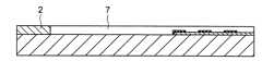
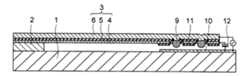
本発明の第1の実施の形態に係るMEMSスイッチは、基板1と、基板1上に形成された固定部2と、下部電極4、下部電極4上に形成された第1の絶縁層5、及び、第1の絶縁層5上に形成された上部電極6を含み、一方の端部が固定部2により支持及び固定された可動梁3と、可動梁3の他方の端部の底面に対向して、基板1上に形成された固定電極10と、固定電極10に対向する領域における下部電極4及び第1の絶縁層5に形成された開口部に、固定電極10に対向する可動梁3の底面よりも下方に突出して、上部電極6と電気的に接続され且つ下部電極4と絶縁されて形成された接点電極9と、下部電極4と固定電極10とを絶縁する一方、接点電極9と固定電極10とが接触し得るように、接点電極9と対向する領域に開口部を有して固定電極10上に形成された第2の絶縁層11と、を備えている。 The MEMS switch according to the first embodiment of the present invention includes a
下部電極4、第1の絶縁層5及び上部電極6を含む可動梁3は、一方の端部が固定部2により支持及び固定されており、他方の端部が上下方向に可動な可動先端部となっている。接点電極9は、通常、可動先端部に形成される。 The
可動梁3の可動先端部、及び、可動先端部に対向する基板1上の部分の一例としての具体的構成は、以下の通りである。 A specific configuration as an example of the movable tip portion of the
基板1上に固定電極10が形成されており、固定電極10を被覆する第2の絶縁層11には、その周縁部より内部に4箇所の開口部が形成されており、それらの開口部において固定電極10の表面が露出している。 A
固定電極10及び第2の絶縁層11は、可動梁3の可動先端部の底面に対向する領域に形成されている。 The
可動梁3の可動先端部の下部電極4及び第1の絶縁層5には、第2の絶縁層11の4箇所の開口部に対向する4箇所の部分、即ち、下部電極4及び第1の絶縁層5の周縁部より内部の4箇所の部分に開口部が形成されている。 The
下部電極4及び第1の絶縁層5の4箇所の開口部には、それぞれ、固定電極10に対向する可動梁3の底面、即ち、本実施の形態においては下部電極4の底面よりも下方に突出して、上部電極6と電気的に接続され且つ下部電極4と絶縁された4個の接点電極9が形成されている。 In the four openings of the
ここで、接点電極9の下方への突出の程度について、固定電極10に対向する可動梁3の底面よりも下方に突出して、という表現を用いている理由は、第2の絶縁層11が、後述するように、基板1側の固定電極10上に形成されていてもよく、又は、可動梁3側の、固定電極10に対向する下部電極4の底面に付加して形成されていてもよいからである。第2の絶縁層11が固定電極10上に形成されている場合には、下部電極4の底面が可動梁3の底面を構成することとなり、第2の絶縁層11が下部電極4の底面に付加して形成されている場合には、第2の絶縁層11の底面が可動梁3の少なくとも可動先端部の底面を構成することとなる。 Here, the reason for using the expression that the degree of the downward protrusion of the
本発明の第1の実施の形態においては、上述のように、第2の絶縁層11は固定電極10上に形成されている。 In the first embodiment of the present invention, the second insulating
以上のような構成の本発明の第1の実施の形態に係るMEMSスイッチにおいて、可動梁3の下部電極4と基板1上の固定電極10との間に静電駆動電圧12を印加すると、両電極間に静電吸引力が発生し、可動梁3の可動先端部が固定電極10に吸引される。 In the MEMS switch according to the first embodiment of the present invention configured as described above, when the
但し、下部電極4と固定電極10とは第2の絶縁層11により絶縁されるので、両電極は短絡せず、静電駆動電圧12が印加されている間、静電吸引力は保持される。 However, since the
一方、固定電極10に対向する可動梁3の底面、即ち、下部電極4の底面よりも下方に突出して形成された4個の接点電極9は、第2の絶縁層11の4箇所の開口部から露出している固定電極10とそれぞれ接触し、固定電極10と可動梁3の上部電極6とが導通する。 On the other hand, the four
ここで、各接点電極9は、静電吸引力を発生させる固定電極10と可動梁3の下部電極4とに周囲を包囲されている。 Here, each
従って、可動梁3が堆積薄膜により形成された剛性の小さいものである場合においても、各接点電極9は、均等且つ充分な強さの力で固定電極10に押し付けられる。 Therefore, even when the
結果として、本発明の第1の実施の形態によれば、接点電極9と固定電極10との間の接触抵抗が低く、耐用寿命が長く、信頼性の高い静電駆動DCコンタクト型MEMSスイッチを実現することができる。 As a result, according to the first embodiment of the present invention, an electrostatically driven DC contact type MEMS switch having a low contact resistance between the
次に、本発明の第1の実施の形態に係る静電駆動DCコンタクト型MEMSスイッチの製造工程の一例について説明する。 Next, an example of a manufacturing process of the electrostatic drive DC contact type MEMS switch according to the first embodiment of the present invention will be described.
図3a乃至図3eは、本発明の第1の実施の形態に係る静電駆動DCコンタクト型MEMSスイッチの各製造工程における構造を示す断面図である。図3a乃至図3eの各断面図は、図1の切断線AAに沿った切断面に相当する部分の断面図である。 3a to 3e are cross-sectional views showing the structure in each manufacturing process of the electrostatically driven DC contact type MEMS switch according to the first embodiment of the present invention. Each of the cross-sectional views of FIGS. 3a to 3e is a cross-sectional view of a portion corresponding to a cut surface along the cutting line AA of FIG.
先ず、図3aに示すように、スパッタリング法及びリフトオフ法を使用して、ガラス基板1上に厚さ300nmのイリジウム(Ir)からなる固定電極10を形成する。さらに、反応性スパッタリング法を使用して、厚さ200nmの酸化シリコンからなる絶縁層11(上記第2の絶縁層11)を形成し、リソグラフィ法及びRIEによりパターニングを行って、絶縁層11の周縁部より内部に4箇所の開口部を開口し、固定電極10の表面を露出させる。 First, as shown in FIG. 3A, a fixed
固定電極10の材料としては、イリジウム(Ir)の他に、金(Au)、白金(Pt)等の貴金属を使用することが可能である。 As a material for the fixed
絶縁層11の材料としては、酸化シリコンの他に、窒化シリコン、酸化アルミニウム等、通常の半導体プロセスにおいて使用される各種の絶縁膜を使用することが可能である。 As a material of the insulating
固定電極10及び絶縁層11を形成後、MOCVD法により窒化シリコン膜を成膜してリソグラフィ法及びRIEによりパターニングを行って、図3bに示すように、固定部2を形成する。さらに、スパッタ法によりアモルファスシリコンからなる犠牲層7を形成して、CMP(化学的機械的研磨法)により固定部2の表面が露出するまで表面研磨及び平坦化を行う。 After the fixed
犠牲層7としては、他の膜材料に対して選択的エッチングが可能な無機材料、金属材料、有機材料等を使用することが可能であるが、本実施の形態ではアモルファスシリコンを使用している。 As the
固定部2及び犠牲層7を形成後、リフトオフ用のレジストパターンを利用してRIEにより犠牲層7のライトエッチングを行い、犠牲層7に深さ400nmのトレンチを形成した後、スパッタ法により金(Au)を堆積させてリフトオフ法によりパターニングを行い、図3cに示すように、接点電極9を形成する。 After the fixing
接点電極9を形成後、スパッタ法並びにリソグラフィ法及びRIEにより、図3dに示すように、厚さ300nmのアルミニウム(Al)からなる下部電極4と、厚さ200nmの酸化シリコンからなる絶縁層5(上記第1の絶縁層5)とを順に形成する。このとき、下部電極4は、接点電極9から離間して直接接触しないようにパターニングを行い、絶縁層5は、下部電極4と接点電極9との間の間隙を埋め込むように形成した上で、接点電極9の上面が露出するようにパターニングを行った。 After the
下部電極4及び絶縁層5を形成後、スパッタ法並びにリソグラフィ法及びRIEにより、図3eに示すように、厚さ1μmのアルミニウム(Al)からなる上部電極6を、接点電極9に電気的に接続されるように形成する。その後、二フッ化キセノン(XeF2)を使用した選択的エッチングにより犠牲層7を除去すると、図1及び図2に示した通りの構造を有する本発明の第1の実施の形態に係る静電駆動DCコンタクト型MEMSスイッチが完成する。After forming the
この本発明の第1の実施の形態に係るMEMSスイッチにおいて、可動梁3の下部電極4と固定電極10との間に0V乃至15Vの静電駆動電圧12を印加して、可動梁3の上部電極6と固定電極10との間の抵抗を測定したところ、108回以上の繰り返し開閉動作を行っても、1Ω以下の非常に低いコンタクト抵抗が安定的に得られた。In the MEMS switch according to the first embodiment of the present invention, an
図4は、本発明の第1の実施の形態に係る静電駆動DCコンタクト型MEMSスイッチの変形例の断面図であり、図1の切断線AAに沿った切断面に相当する部分の断面図である。 4 is a cross-sectional view of a modification of the electrostatically driven DC contact type MEMS switch according to the first embodiment of the present invention, and is a cross-sectional view of a portion corresponding to a cut surface along the cutting line AA of FIG. It is.
図4に示す第1の実施の形態の変形例は、図1に示す第1の実施の形態において基板1側の固定電極10上に形成されていた第2の絶縁層11が、可動梁3側の、基板1に対向する下部電極4の底面に付加して形成されているものである。 In the modification of the first embodiment shown in FIG. 4, the second insulating
即ち、図4に示す第1の実施の形態の変形例における第2の絶縁層11は、下部電極4と固定電極10とを絶縁する一方、接点電極9と固定電極10とが接触し得るように、接点電極9周辺の、固定電極10に対向する下部電極4の底面に接点電極9を避けて形成されている。 That is, the second insulating
第2の絶縁層11は、形成されている部位が異なっているが、下部電極4と固定電極10との間に静電駆動電圧12が印加されたときに、下部電極4と固定電極10との短絡を防止するという役割は全く同様である。 The second insulating
この変形例においても、第1の実施の形態と同様に、接点電極9と固定電極10との間の接触抵抗が低く、耐用寿命が長く、信頼性の高い静電駆動DCコンタクト型MEMSスイッチを実現することができる。 Also in this modified example, as in the first embodiment, an electrostatically driven DC contact type MEMS switch having a low contact resistance between the
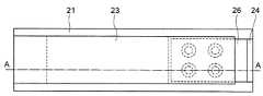
図5は、本発明の第2の実施の形態に係る静電駆動DCコンタクト型MEMSスイッチの平面図であり、図6は、本発明の第2の実施の形態に係るMEMSスイッチの断面図であって、図5の切断線AAに沿った断面図である。 FIG. 5 is a plan view of an electrostatically driven DC contact type MEMS switch according to a second embodiment of the present invention, and FIG. 6 is a cross-sectional view of the MEMS switch according to the second embodiment of the present invention. FIG. 6 is a cross-sectional view taken along a cutting line AA in FIG. 5.
本発明の第2の実施の形態に係るMEMSスイッチは、基板21と、基板21上に形成された固定部22と、一方の端部が固定部22により支持及び固定された導電性の可動梁23と、可動梁23の他方の端部の底面に対向する基板21上の領域に形成された固定下部電極24と、固定下部電極24の一部を露出させる開口部を有して固定下部電極24上に形成された第1の絶縁層25と、第1の絶縁層25上に形成された固定上部電極26と、固定上部電極26上に形成された第2の絶縁層27と、固定下部電極24と電気的に接続され且つ固定上部電極26と絶縁されて第2の絶縁層27の上面よりも上方に突出して第1の絶縁層25の開口部に形成された接点電極28と、を備えている。 The MEMS switch according to the second embodiment of the present invention includes a
本発明の第2の実施の形態に係るMEMSスイッチにおいては、静電駆動電圧29が印加される固定上部電極26、高周波信号が通過する固定下部電極24、可動梁23と固定下部電極24とを導通させる接点電極28等が総て基板21上に形成されており、可動梁23は一層構造を有している。 In the MEMS switch according to the second embodiment of the present invention, a fixed
導電性の材料で形成された可動梁23は、一方の端部が固定部22により支持されて基板21上に固定されており、他方の端部、即ち、可動先端部が接点電極28及び固定上部電極26の上方に延在している。 The
第1の絶縁層25、固定上部電極26及び第2の絶縁層27には、例えば、それらの周縁部より内部の4箇所の部分に開口部が形成されている。それらの開口部内部には、固定下部電極24と電気的に接続され且つ固定上部電極26と絶縁されて第2の絶縁層27の上面よりも上方に突出した4個の接点電極28がそれぞれ形成されている。 In the first insulating
可動梁23と固定上部電極26との間に静電駆動電圧29を印加することにより、両電極間に静電吸引力が発生し、可動梁23の可動先端部が上部固定電極26に吸引される。 By applying an
但し、可動梁23と上部固定電極26とは第2の絶縁層27により絶縁されるので、両電極は短絡せず、静電駆動電圧29が印加されている間、静電吸引力は保持される。 However, since the
一方、第2の絶縁層27の上面よりも上方に突出して形成された4個の接点電極28は、可動梁23の可動先端部とそれぞれ接触し、可動梁23と固定下部電極24とが導通する。 On the other hand, the four
このとき、各接点電極28は、静電吸引力を発生させる固定上部電極26と可動梁23の可動先端部とに周囲を包囲されている。 At this time, each
従って、可動梁23が堆積薄膜により形成された剛性の小さいものである場合においても、可動梁23の可動先端部は、均等且つ充分な強さの力で各接点電極28に押し付けられる。 Therefore, even when the
結果として、本発明の第2の実施の形態によれば、接点電極28と導電性の可動梁23との間の接触抵抗が低く、耐用寿命が長く、信頼性の高い静電駆動DCコンタクト型MEMSスイッチを実現することができる。 As a result, according to the second embodiment of the present invention, the contact resistance between the
尚、本発明の第2の実施の形態においては、第2の絶縁層27は、上述のように、固定上部電極26上に形成されている。 In the second embodiment of the present invention, the second insulating
しかし、本発明の第2の実施の形態においても、第2の絶縁層27が、基板21側の固定上部電極26上ではなく、固定上部電極26に対向する可動梁23の底面に付加して形成されている変形例を構成することが可能である。 However, also in the second embodiment of the present invention, the second insulating
その場合の本発明の第2の実施の形態に係るMEMSスイッチの変形例は、基板21と、基板21上に形成された固定部22と、一方の端部が固定部22により支持及び固定された導電性の可動梁23と、可動梁23の他方の端部の底面に対向する基板21上の領域に形成された固定下部電極24と、固定下部電極24の一部を露出させる開口部を有して固定下部電極24上に形成された第1の絶縁層25と、第1の絶縁層25上に形成された固定上部電極26と、固定下部電極24と電気的に接続され且つ固定上部電極26と絶縁されて固定上部電極26の上面よりも上方に突出して第1の絶縁層25の開口部に形成された接点電極28と、接点電極28と対向する領域に開口部を有して可動梁23の他方の端部の底面に形成された第2の絶縁層(27)と、を備えているものとなる。 In this case, a modification of the MEMS switch according to the second embodiment of the present invention includes a
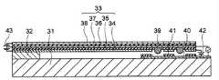
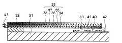
図7は、本発明の第3の実施の形態に係る静電駆動DCコンタクト型MEMSスイッチの平面図であり、図8は、本発明の第3の実施の形態に係るMEMSスイッチの断面図であって、図7の切断線AAに沿った断面図である。 FIG. 7 is a plan view of an electrostatically driven DC contact type MEMS switch according to a third embodiment of the present invention, and FIG. 8 is a cross-sectional view of the MEMS switch according to the third embodiment of the present invention. FIG. 8 is a cross-sectional view taken along a cutting line AA in FIG. 7.
本発明の第3の実施の形態に係るMEMSスイッチは、基板31と、基板31上に形成された固定部32と、下部電極34、下部電極34上に形成された下部圧電層35、下部圧電層35上に形成された中間電極36、中間電極36上に形成された上部圧電層37、及び、上部圧電層37上に形成された上部電極38を含み、一方の端部が固定部32により支持及び固定された可動梁33と、可動梁33の他方の端部の底面に対向して、基板31上に形成された固定電極40と、固定電極40に対向する領域における下部電極34及び下部圧電層35に形成された開口部に、固定電極40に対向する可動梁33の底面よりも下方に突出して、中間電極36と電気的に接続され且つ下部電極34と絶縁されて形成された接点電極39と、下部電極34と固定電極40とを絶縁する一方、接点電極39と固定電極40とが接触し得るように、接点電極39と対向する領域に開口部を有して固定電極40上に形成された絶縁層41と、を備えている。 The MEMS switch according to the third embodiment of the present invention includes a
本発明の第3の実施の形態に係るMEMSスイッチは、第1乃至第2の実施の形態と同様の静電駆動機構に加えて圧電バイモルフ駆動機構も兼備したハイブリッド型駆動機構を備えている。 The MEMS switch according to the third embodiment of the present invention includes a hybrid drive mechanism that also has a piezoelectric bimorph drive mechanism in addition to the electrostatic drive mechanism similar to that of the first and second embodiments.
下部電極34、下部圧電層35、中間電極36、上部圧電層37及び上部電極38を含む可動梁33は、一方の端部が固定部32により支持及び固定されており、他方の端部が上下方向に可動な可動先端部となっている。接点電極99は、通常、可動先端部に形成される。 The
可動梁33の可動先端部、及び、可動先端部に対向する基板31上の部分の一例としての具体的構成は、以下の通りである。 A specific configuration as an example of the movable tip portion of the
基板31上には固定電極40が形成されており、固定電極40を被覆する絶縁層41には、その周縁部より内部に4箇所の開口部が形成されており、それらの開口部において固定電極40の表面が露出している。 A fixed
固定電極40及び絶縁層41は、可動梁33の可動先端部に対向する領域に形成されている。 The fixed
可動梁33の可動先端部の下部電極34及び下部圧電層35には、絶縁層41の4箇所の開口部に対向する4箇所の部分、即ち、下部電極34及び下部圧電層35の周縁部より内部の4箇所の部分に開口部が形成されている。 The lower electrode 34 and the lower
下部電極34及び下部圧電層35の4箇所の開口部には、それぞれ、固定電極40に対向する可動梁33の底面、即ち、本実施の形態においては下部電極34の底面よりも下方に突出して、中間電極36と電気的に接続され且つ下部電極34と絶縁された4個の接点電極39が形成されている。 The four openings of the lower electrode 34 and the lower
ここで、接点電極39の下方への突出の程度について、基板31に対向する可動梁33の底面よりも下方に突出して、という表現を用いている理由は、絶縁層41が、後述するように、基板31側の固定電極40上に形成されていてもよく、又は、可動梁33側の、固定電極40に対向する下部電極34の底面に付加して形成されていてもよいからである。絶縁層41が固定電極40上に形成されている場合には、下部電極34の底面が可動梁33の底面を構成することとなり、絶縁層41が下部電極34の底面に付加して形成されている場合には、絶縁層41の底面が可動梁33の少なくとも可動先端部の底面を構成することとなる。 Here, the reason why the expression that the
本発明の第3の実施の形態においては、上述のように、絶縁層41は固定電極40上に形成されている。 In the third embodiment of the present invention, the insulating
可動梁33の下部圧電層35及び上部圧電層37は、層面に垂直な同一方向に分極しており、下部電極34及び中間電極36間と中間電極36及び上部電極38間とに逆バイアスの圧電駆動電圧43を印加することにより、下部圧電層35は層面内に収縮し、上部圧電層37は層面内に伸長するため、可動梁33は上に凸状に撓み、可動先端部が基板31に接触する。尚、本実施の形態においては、下部圧電層35及び上部圧電層37として、スパッタ法により作製した、厚さ方向にc軸配向した厚さ0.5μmの窒化アルミニウム(AlN)圧電膜を使用している。 The lower
一方、可動梁33の下部電極34と固定電極40との間にも静電駆動電圧42を印加すると、両電極間に静電吸引力が発生し、可動梁33の可動先端部が固定電極40に吸引される。 On the other hand, when an
但し、固定電極40上には絶縁層41が形成されているので、可動梁33の下部電極34と固定電極40とは短絡せずに静電吸引力は保持される。従って、可動梁33の接点電極39と固定電極40とが接触し、可動梁33の中間電極36と固定電極40とが接点電極39を介して導通する。 However, since the insulating
ここで、各接点電極39は、静電吸引力を発生させる固定電極40と可動梁33の下部電極34とに周囲を包囲されている。 Here, each
従って、可動梁33が堆積薄膜により形成された剛性の小さいものである場合においても、各接点電極39は、均等且つ充分な強さの力で固定電極40に押し付けられる。 Therefore, even when the
尚、可動梁33の下部電極34は、圧電バイモルフ駆動電極及び静電駆動電極の二重の役割を果たしており、また、中間電極36は、圧電バイモルフ駆動電極及び高周波信号電極の二重の役割を果たしている。 The lower electrode 34 of the
圧電バイモルフ駆動の場合は、低電圧で大きな変形が得られるという特徴があるが、可動梁33の可動先端部の押し付け力は弱い。一方、静電駆動の場合は、静電吸引力は電極間距離の−2乗に比例するため、電極間距離が長いと大きな駆動電圧が必要であるが、二つの電極が電極間に絶縁層を介して接触した場合には大きな吸引力を発揮する。 The piezoelectric bimorph drive has a feature that a large deformation can be obtained at a low voltage, but the pressing force of the movable tip of the
従って、本実施の形態のような圧電駆動及び静電駆動を兼備したハイブリッド型駆動機構においては、電極間が離れている間は主として圧電駆動により可動梁33の可動先端部が変位し、可動梁33の可動先端部と固定電極40とが近づいたときは主として静電駆動により大きな吸引力が得られるという利点がある。 Therefore, in the hybrid drive mechanism having both piezoelectric drive and electrostatic drive as in the present embodiment, the movable tip of the
よって、本発明の第3の実施の形態によれば、駆動電圧が低く、接点電極39と固定電極10との間の接触抵抗が低く、耐用寿命が長く、信頼性の高い静電駆動DCコンタクト型MEMSスイッチを実現することができる。 Therefore, according to the third embodiment of the present invention, the drive voltage is low, the contact resistance between the
具体的には、静電駆動のみの第1の実施の形態に係るMEMSスイッチでは、前述したように15Vの駆動電圧が必要であったのに対し、可動梁33の長さが400μm、接点電極39と固定電極40との間隔が2μmに設定された第3の実施の形態に係るMEMSスイッチの場合には、静電駆動と圧電駆動とのハイブリッド駆動の動作電圧は6Vで充分であった。 Specifically, in the MEMS switch according to the first embodiment only for electrostatic driving, the driving voltage of 15 V is necessary as described above, whereas the length of the
尚、上述のように、本発明の第3の実施の形態においては、絶縁層41は、固定電極40上に形成されている。 As described above, the insulating
しかし、本発明の第3の実施の形態においても、絶縁層41が、基板31側の固定電極40上ではなく、固定電極40に対向する可動梁33側の下部電極34の底面に付加して形成されている第1の変形例を構成することが可能である。 However, also in the third embodiment of the present invention, the insulating
その場合の本発明の第3の実施の形態に係るMEMSスイッチの第1の変形例は、基板31と、基板31上に形成された固定部32と、下部電極34、下部電極34上に形成された下部圧電層35、下部圧電層35上に形成された中間電極36、中間電極36上に形成された上部圧電層37、及び、上部圧電層37上に形成された上部電極38を含み、一方の端部が固定部32により支持及び固定された可動梁33と、可動梁33の他方の端部の底面に対向して、基板31上に形成された固定電極40と、固定電極40に対向する領域における下部電極34及び下部圧電層35に形成された開口部に、固定電極40に対向する可動梁33の底面よりも下方に突出して、中間電極36と電気的に接続され且つ下部電極34と絶縁されて形成された接点電極39と、下部電極34と固定電極40とを絶縁する一方、接点電極39と固定電極40とが接触し得るように、固定電極40に対向する下部電極34の底面に接点電極39を避けて形成された絶縁層41と、を備えているものとなる。 In this case, the first modification of the MEMS switch according to the third embodiment of the present invention is formed on the
図9は、本発明の第3の実施の形態に係る静電駆動DCコンタクト型MEMSスイッチの第2の変形例の平面図であり、図10は、本発明の第3の実施の形態に係るMEMSスイッチの第2の変形例の断面図であって、図9の切断線AAに沿った断面図である。 FIG. 9 is a plan view of a second modification of the electrostatically driven DC contact type MEMS switch according to the third embodiment of the present invention, and FIG. 10 relates to the third embodiment of the present invention. It is sectional drawing of the 2nd modification of a MEMS switch, Comprising: It is sectional drawing along the cutting line AA of FIG.
本発明の第3の実施の形態の第2の変形例の全体的な構成は、第3の実施の形態とほぼ同様であるが、基板31上の固定電極40が、可動梁33の長手方向と垂直な方向に沿って、第1の固定電極40aと第2の固定電極40bとに分割して形成されており、接点電極39が、第1の固定電極40aと第2の固定電極40bとに対向する位置にそれぞれ形成されている点が異なっている。 The overall configuration of the second modification of the third embodiment of the present invention is substantially the same as that of the third embodiment, except that the fixed
即ち、本発明の第3の実施の形態の第2の変形例における第1の固定電極40aと第2の固定電極40bとは、可動梁33の長手方向に沿った分割領域を挟んで、可動梁33の長手方向と垂直な方向に沿って分割して形成されている。 That is, the first
上記構成から分かるように、本発明の第3の実施の形態の第2の変形例は、いわゆるシリーズ型スイッチの例である。 As can be seen from the above configuration, the second modification of the third embodiment of the present invention is an example of a so-called series switch.
この第2の変形例においては、可動梁33が基板31に接触してスイッチが閉状態になったときに、高周波信号は、固定電極40a−接触電極39−中間電極36−接触電極39−固定電極40bの経路に沿って流れることができ、高周波信号が可動梁33の中間電極36を流れる距離を著しく短縮できるため、直列抵抗成分を減少させることが可能である。 In the second modification, when the
尚、本発明の第3の実施の形態の第2の変形例においても、絶縁層41が、基板31側の固定電極40上ではなく、固定電極40に対向する可動梁33側の下部電極34の底面に付加して形成されている更なる変形例を構成することが可能である。 Also in the second modification of the third embodiment of the present invention, the insulating
1,21,31 基板
2,22,32 固定部
3,23,33 可動梁
4,34 下部電極
5,11,25,27,41 絶縁層
6,38 上部電極
7 犠牲層
9,28,39 接点電極
10,40 固定電極
12,29 静電駆動電圧
24 固定下部電極
26 固定上部電極
37 上部圧電層
36 中間電極
35 下部圧電層1, 21, 31
Claims (17)
Translated fromJapanese前記基板上に形成された固定部と、
下部電極、前記下部電極上に形成された第1の絶縁層、及び、前記第1の絶縁層上に形成された上部電極を含み、一方の端部が前記固定部により支持及び固定された可動梁と、
前記可動梁の他方の端部の底面に対向して、前記基板上に形成された固定電極と、
前記固定電極に対向する領域における前記下部電極及び前記第1の絶縁層に形成された開口部に、前記固定電極に対向する前記可動梁の底面よりも下方に突出して、前記上部電極と電気的に接続され且つ前記下部電極と絶縁されて形成された接点電極と、
前記下部電極と前記固定電極とを絶縁する一方、前記接点電極と前記固定電極とが接触し得るように、前記接点電極と対向する領域に開口部を有して前記固定電極上に形成された、又は、前記固定電極に対向する前記下部電極の底面に前記接点電極を避けて形成された第2の絶縁層と、
を備え、
前記下部電極と前記固定電極との間には、静電駆動電圧が印加されることを特徴とするMEMSスイッチ。A substrate,
A fixing part formed on the substrate;
A movable part including a lower electrode, a first insulating layer formed on the lower electrode, and an upper electrode formed on the first insulating layer, one end of which is supported and fixed by the fixing part With a beam,
A fixed electrode formed on the substrate, facing the bottom surface of the other end of the movable beam,
The lower electrode in the region facing the fixed electrode and the opening formed in the first insulating layer protrude downward from the bottom surface of the movable beam facing the fixed electrode, and are electrically connected to the upper electrode. A contact electrode connected to the lower electrode and insulated from the lower electrode;
The lower electrode and the fixed electrode are formed on the fixed electrode with an opening in a region facing the contact electrode so that the contact electrode and the fixed electrode can be in contact with each other. Or a second insulating layer formed avoiding the contact electrode on the bottom surface of the lower electrode facing the fixed electrode;
Equipped witha,
An MEMS switch, wherein an electrostatic drive voltage is applied between the lower electrode and the fixed electrode .
前記基板上に形成された固定部と、
一方の端部が前記固定部により支持及び固定された導電性の可動梁と、
前記可動梁の他方の端部の底面に対向する前記基板上の領域に形成された固定下部電極と、
前記固定下部電極の一部を露出させる開口部を有して前記固定下部電極上に形成された第1の絶縁層と、
前記第1の絶縁層上に形成された固定上部電極と、
前記固定上部電極上に形成された第2の絶縁層と、
前記固定下部電極と電気的に接続され且つ前記固定上部電極と絶縁されて前記第2の絶縁層の上面よりも上方に突出して前記第1の絶縁層の前記開口部に形成された接点電極と、
を備え、
前記可動梁と前記固定上部電極との間には、静電駆動電圧が印加されることを特徴とするMEMSスイッチ。A substrate,
A fixing part formed on the substrate;
A conductive movable beam having one end supported and fixed by the fixed portion;
A fixed lower electrode formed in a region on the substrate facing the bottom surface of the other end of the movable beam;
A first insulating layer formed on the fixed lower electrode with an opening exposing a portion of the fixed lower electrode;
A fixed upper electrode formed on the first insulating layer;
A second insulating layer formed on the fixed upper electrode;
A contact electrode electrically connected to the fixed lower electrode and insulated from the fixed upper electrode, protruding above the upper surface of the second insulating layer and formed in the opening of the first insulating layer; ,
Equipped witha,
A MEMS switch, wherein an electrostatic drive voltage is applied between the movable beam and the fixed upper electrode .
前記基板上に形成された固定部と、
一方の端部が前記固定部により支持及び固定された導電性の可動梁と、
前記可動梁の他方の端部の底面に対向する前記基板上の領域に形成された固定下部電極と、
前記固定下部電極の一部を露出させる開口部を有して前記固定下部電極上に形成された第1の絶縁層と、
前記第1の絶縁層上に形成された固定上部電極と、
前記固定下部電極と電気的に接続され且つ前記固定上部電極と絶縁されて前記固定上部電極の上面よりも上方に突出して前記第1の絶縁層の前記開口部に形成された接点電極と、
前記接点電極と対向する領域に開口部を有して前記可動梁の前記他方の端部の底面に形成された第2の絶縁層と、
を備え、
前記可動梁と前記固定上部電極との間には、静電駆動電圧が印加されることを特徴とするMEMSスイッチ。A substrate,
A fixing part formed on the substrate;
A conductive movable beam having one end supported and fixed by the fixed portion;
A fixed lower electrode formed in a region on the substrate facing the bottom surface of the other end of the movable beam;
A first insulating layer formed on the fixed lower electrode with an opening exposing a portion of the fixed lower electrode;
A fixed upper electrode formed on the first insulating layer;
A contact electrode electrically connected to the fixed lower electrode and insulated from the fixed upper electrode and protruding above the upper surface of the fixed upper electrode and formed in the opening of the first insulating layer;
A second insulating layer formed on the bottom surface of the other end of the movable beam having an opening in a region facing the contact electrode;
Equipped witha,
A MEMS switch, wherein an electrostatic drive voltage is applied between the movable beam and the fixed upper electrode .
前記基板上に形成された固定部と、
下部電極、前記下部電極上に形成された下部圧電層、前記下部圧電層上に形成された中間電極、前記中間電極上に形成された上部圧電層、及び、前記上部圧電層上に形成された上部電極を含み、一方の端部が前記固定部により支持及び固定された可動梁と、
前記可動梁の他方の端部の底面に対向して、前記基板上に形成された固定電極と、
前記固定電極に対向する領域における前記下部電極及び前記下部圧電層に形成された開口部に、前記固定電極に対向する前記可動梁の底面よりも下方に突出して、前記中間電極と電気的に接続され且つ前記下部電極と絶縁されて形成された接点電極と、
前記下部電極と前記固定電極とを絶縁する一方、前記接点電極と前記固定電極とが接触し得るように、前記接点電極と対向する領域に開口部を有して前記固定電極上に形成された、又は、前記固定電極に対向する前記下部電極の底面に前記接点電極を避けて形成された絶縁層と、
を備え、
前記下部電極と前記固定電極との間には、静電駆動電圧が印加されることを特徴とするMEMSスイッチ。A substrate,
A fixing part formed on the substrate;
A lower electrode; a lower piezoelectric layer formed on the lower electrode; an intermediate electrode formed on the lower piezoelectric layer; an upper piezoelectric layer formed on the intermediate electrode; and an upper piezoelectric layer formed on the upper piezoelectric layer A movable beam including an upper electrode, one end of which is supported and fixed by the fixed portion;
A fixed electrode formed on the substrate, facing the bottom surface of the other end of the movable beam,
An opening formed in the lower electrode and the lower piezoelectric layer in a region facing the fixed electrode projects below the bottom surface of the movable beam facing the fixed electrode and is electrically connected to the intermediate electrode. And a contact electrode formed insulated from the lower electrode;
The lower electrode and the fixed electrode are formed on the fixed electrode with an opening in a region facing the contact electrode so that the contact electrode and the fixed electrode can be in contact with each other. Or an insulating layer formed avoiding the contact electrode on the bottom surface of the lower electrode facing the fixed electrode;
Equipped witha,
An MEMS switch, wherein an electrostatic drive voltage is applied between the lower electrode and the fixed electrode .
Priority Applications (2)
| Application Number | Priority Date | Filing Date | Title |
|---|---|---|---|
| JP2006201064AJP4234737B2 (en) | 2006-07-24 | 2006-07-24 | MEMS switch |
| US11/673,984US7675393B2 (en) | 2006-07-24 | 2007-02-12 | MEMS switch |
Applications Claiming Priority (1)
| Application Number | Priority Date | Filing Date | Title |
|---|---|---|---|
| JP2006201064AJP4234737B2 (en) | 2006-07-24 | 2006-07-24 | MEMS switch |
Publications (2)
| Publication Number | Publication Date |
|---|---|
| JP2008027812A JP2008027812A (en) | 2008-02-07 |
| JP4234737B2true JP4234737B2 (en) | 2009-03-04 |
Family
ID=38970396
Family Applications (1)
| Application Number | Title | Priority Date | Filing Date |
|---|---|---|---|
| JP2006201064AExpired - Fee RelatedJP4234737B2 (en) | 2006-07-24 | 2006-07-24 | MEMS switch |
Country Status (2)
| Country | Link |
|---|---|
| US (1) | US7675393B2 (en) |
| JP (1) | JP4234737B2 (en) |
Families Citing this family (22)
| Publication number | Priority date | Publication date | Assignee | Title |
|---|---|---|---|---|
| DE102004026654B4 (en)* | 2004-06-01 | 2009-07-09 | Fraunhofer-Gesellschaft zur Förderung der angewandten Forschung e.V. | Micromechanical RF switching element and method of manufacture |
| US8093968B2 (en)* | 2005-11-24 | 2012-01-10 | Panasonic Corporation | Microelectromechanical element and electromechanical switch using the same |
| JP4492677B2 (en)* | 2007-11-09 | 2010-06-30 | セイコーエプソン株式会社 | Active matrix device, electro-optical display device, and electronic apparatus |
| WO2009067222A1 (en)* | 2007-11-19 | 2009-05-28 | Xcom Wireless, Inc. | Microfabricated cantilever slider with asymmetric spring constant |
| JP2009194291A (en)* | 2008-02-18 | 2009-08-27 | Toshiba Corp | Actuator |
| JP2009201317A (en)* | 2008-02-25 | 2009-09-03 | Toshiba Corp | Method of controlling semiconductor device and electrostatic actuator |
| JP5081038B2 (en) | 2008-03-31 | 2012-11-21 | パナソニック株式会社 | MEMS switch and manufacturing method thereof |
| JP2010036280A (en)* | 2008-08-01 | 2010-02-18 | Fuji Electric Holdings Co Ltd | Method for manufacturing MEMS structure |
| US8779886B2 (en)* | 2009-11-30 | 2014-07-15 | General Electric Company | Switch structures |
| JP5598653B2 (en) | 2010-02-01 | 2014-10-01 | ソニー株式会社 | Reed switch |
| DE102010002818B4 (en)* | 2010-03-12 | 2017-08-31 | Robert Bosch Gmbh | Method for producing a micromechanical component |
| DE102010012607B4 (en) | 2010-03-24 | 2012-01-26 | Eads Deutschland Gmbh | RF MEMS switch |
| US8576029B2 (en)* | 2010-06-17 | 2013-11-05 | General Electric Company | MEMS switching array having a substrate arranged to conduct switching current |
| FR2964243A1 (en)* | 2010-08-27 | 2012-03-02 | Commissariat Energie Atomique | INTERMITTENT CONTACT DEVICE IMPROVED BY DIELECTROPHORESIS |
| FR2966813A1 (en)* | 2010-10-29 | 2012-05-04 | Thales Sa | ELECTROMECHANICAL MICROSYSTEM (MEMS). |
| US8673670B2 (en)* | 2011-12-15 | 2014-03-18 | International Business Machines Corporation | Micro-electro-mechanical system (MEMS) structures and design structures |
| US9251984B2 (en)* | 2012-12-27 | 2016-02-02 | Intel Corporation | Hybrid radio frequency component |
| US10566140B2 (en)* | 2013-08-01 | 2020-02-18 | Cavendish Kinetics, Inc. | DVC utilizing MEMS resistive switches and MIM capacitors |
| US9162868B2 (en)* | 2013-11-27 | 2015-10-20 | Infineon Technologies Ag | MEMS device |
| GB201414811D0 (en)* | 2014-08-20 | 2014-10-01 | Ibm | Electromechanical switching device with electrodes comprising 2D layered materials having distinct functional areas |
| CN108352277B (en)* | 2015-11-16 | 2021-02-26 | 卡文迪什动力有限公司 | Naturally closed MEMS switch for ESD protection |
| US20170143103A1 (en)* | 2015-11-19 | 2017-05-25 | Giselle Howard | Anti-wrinkling pad and method |
Family Cites Families (16)
| Publication number | Priority date | Publication date | Assignee | Title |
|---|---|---|---|---|
| DE19736674C1 (en)* | 1997-08-22 | 1998-11-26 | Siemens Ag | Micromechanical electrostatic relay |
| US6127908A (en)* | 1997-11-17 | 2000-10-03 | Massachusetts Institute Of Technology | Microelectro-mechanical system actuator device and reconfigurable circuits utilizing same |
| US6046659A (en)* | 1998-05-15 | 2000-04-04 | Hughes Electronics Corporation | Design and fabrication of broadband surface-micromachined micro-electro-mechanical switches for microwave and millimeter-wave applications |
| US6229683B1 (en)* | 1999-06-30 | 2001-05-08 | Mcnc | High voltage micromachined electrostatic switch |
| US6396368B1 (en)* | 1999-11-10 | 2002-05-28 | Hrl Laboratories, Llc | CMOS-compatible MEM switches and method of making |
| DE60229675D1 (en)* | 2001-11-09 | 2008-12-11 | Wispry Inc | Three-layer beam MEMS device and related methods |
| US7098577B2 (en)* | 2002-10-21 | 2006-08-29 | Hrl Laboratories, Llc | Piezoelectric switch for tunable electronic components |
| KR100513723B1 (en) | 2002-11-18 | 2005-09-08 | 삼성전자주식회사 | MicroElectro Mechanical system switch |
| FR2848331B1 (en)* | 2002-12-10 | 2005-03-11 | Commissariat Energie Atomique | MICRO-MECHANICAL SWITCH AND METHOD OF MAKING SAME |
| US6962832B2 (en)* | 2004-02-02 | 2005-11-08 | Wireless Mems, Inc. | Fabrication method for making a planar cantilever, low surface leakage, reproducible and reliable metal dimple contact micro-relay MEMS switch |
| JP4496091B2 (en) | 2004-02-12 | 2010-07-07 | 株式会社東芝 | Thin film piezoelectric actuator |
| JP4447940B2 (en) | 2004-02-27 | 2010-04-07 | 富士通株式会社 | Microswitching device manufacturing method and microswitching device |
| JP4377740B2 (en) | 2004-04-28 | 2009-12-02 | 株式会社東芝 | Piezoelectric drive type MEMS element and mobile communication device having this piezoelectric drive type MEMS element |
| JP4037394B2 (en) | 2004-09-16 | 2008-01-23 | 株式会社東芝 | Micro mechanical devices |
| JP2006093463A (en) | 2004-09-24 | 2006-04-06 | Toshiba Corp | Piezoelectric MEMS element and tunable filter |
| JP4580826B2 (en) | 2005-06-17 | 2010-11-17 | 株式会社東芝 | Micromechanical devices, microswitches, variable capacitance capacitors, high-frequency circuits, and optical switches |
- 2006
- 2006-07-24JPJP2006201064Apatent/JP4234737B2/ennot_activeExpired - Fee Related
- 2007
- 2007-02-12USUS11/673,984patent/US7675393B2/ennot_activeExpired - Fee Related
Also Published As
| Publication number | Publication date |
|---|---|
| JP2008027812A (en) | 2008-02-07 |
| US7675393B2 (en) | 2010-03-09 |
| US20080017489A1 (en) | 2008-01-24 |
Similar Documents
| Publication | Publication Date | Title |
|---|---|---|
| JP4234737B2 (en) | MEMS switch | |
| US8390173B2 (en) | MEMS switch and method of manufacturing the MEMS switch | |
| CN101276707B (en) | MEMS device and portable communication terminal with said MEMS device | |
| US7256670B2 (en) | Diaphragm activated micro-electromechanical switch | |
| US7343655B2 (en) | Manufacturing methods of micro electromechanical switch | |
| US7545081B2 (en) | Piezoelectric RF MEMS device and method of fabricating the same | |
| JP4465341B2 (en) | High frequency micromachine switch and method of manufacturing the same | |
| JP2004001186A (en) | MEMS device and manufacturing method thereof | |
| JP4879760B2 (en) | Microswitching device and method for manufacturing microswitching device | |
| JP2006294591A (en) | Electrostatic micro-contact switch, its manufacturing method, and apparatus using the switch | |
| KR100516278B1 (en) | Contact switch and apparatus provided with contact switch | |
| JP4466081B2 (en) | MEMS element | |
| JP3651404B2 (en) | Electrostatic micro relay, and radio apparatus and measuring apparatus using the electrostatic micro relay | |
| JP5870616B2 (en) | MEMS switch and manufacturing method thereof | |
| JP4174761B2 (en) | Mechanism device manufacturing method and mechanism device | |
| US8519284B2 (en) | Electronic device | |
| JP2009252598A (en) | Mems switch | |
| JP2006236765A (en) | Electromechanical switch and manufacturing method thereof | |
| JPH11120884A (en) | Electrostatic micro relay | |
| JP2006164989A (en) | Electrostatic micro-relay | |
| JP2004214135A (en) | Micro relay and device equipped with micro relay | |
| JP2013114755A (en) | Switch device and method of manufacturing the same |
Legal Events
| Date | Code | Title | Description |
|---|---|---|---|
| A621 | Written request for application examination | Free format text:JAPANESE INTERMEDIATE CODE: A621 Effective date:20080326 | |
| A977 | Report on retrieval | Free format text:JAPANESE INTERMEDIATE CODE: A971007 Effective date:20080916 | |
| A131 | Notification of reasons for refusal | Free format text:JAPANESE INTERMEDIATE CODE: A131 Effective date:20080924 | |
| A521 | Request for written amendment filed | Free format text:JAPANESE INTERMEDIATE CODE: A523 Effective date:20081120 | |
| TRDD | Decision of grant or rejection written | ||
| A01 | Written decision to grant a patent or to grant a registration (utility model) | Free format text:JAPANESE INTERMEDIATE CODE: A01 Effective date:20081205 | |
| A01 | Written decision to grant a patent or to grant a registration (utility model) | Free format text:JAPANESE INTERMEDIATE CODE: A01 | |
| A61 | First payment of annual fees (during grant procedure) | Free format text:JAPANESE INTERMEDIATE CODE: A61 Effective date:20081211 | |
| FPAY | Renewal fee payment (event date is renewal date of database) | Free format text:PAYMENT UNTIL: 20111219 Year of fee payment:3 | |
| FPAY | Renewal fee payment (event date is renewal date of database) | Free format text:PAYMENT UNTIL: 20121219 Year of fee payment:4 | |
| FPAY | Renewal fee payment (event date is renewal date of database) | Free format text:PAYMENT UNTIL: 20121219 Year of fee payment:4 | |
| FPAY | Renewal fee payment (event date is renewal date of database) | Free format text:PAYMENT UNTIL: 20131219 Year of fee payment:5 | |
| LAPS | Cancellation because of no payment of annual fees |