JP4234101B2 - Gallium nitride compound semiconductor device - Google Patents
Gallium nitride compound semiconductor deviceDownload PDFInfo
- Publication number
- JP4234101B2 JP4234101B2JP2004521142AJP2004521142AJP4234101B2JP 4234101 B2JP4234101 B2JP 4234101B2JP 2004521142 AJP2004521142 AJP 2004521142AJP 2004521142 AJP2004521142 AJP 2004521142AJP 4234101 B2JP4234101 B2JP 4234101B2
- Authority
- JP
- Japan
- Prior art keywords
- layer
- alingan
- composition ratio
- less
- light emitting
- Prior art date
- Legal status (The legal status is an assumption and is not a legal conclusion. Google has not performed a legal analysis and makes no representation as to the accuracy of the status listed.)
- Expired - Lifetime
Links
- 229910002601GaNInorganic materials0.000titleclaimsdescription31
- 239000004065semiconductorSubstances0.000titleclaimsdescription9
- -1Gallium nitride compoundChemical class0.000titleclaims2
- 239000000203mixtureSubstances0.000claimsdescription56
- 230000004888barrier functionEffects0.000claimsdescription42
- JMASRVWKEDWRBT-UHFFFAOYSA-NGallium nitrideChemical compound[Ga]#NJMASRVWKEDWRBT-UHFFFAOYSA-N0.000claimsdescription13
- 239000000758substrateSubstances0.000claimsdescription6
- 150000001875compoundsChemical class0.000claimsdescription5
- 239000010410layerSubstances0.000description190
- JLTRXTDYQLMHGR-UHFFFAOYSA-NtrimethylaluminiumChemical compoundC[Al](C)CJLTRXTDYQLMHGR-UHFFFAOYSA-N0.000description16
- 238000005253claddingMethods0.000description15
- 239000007789gasSubstances0.000description6
- 229910002704AlGaNInorganic materials0.000description5
- 230000007423decreaseEffects0.000description5
- 230000000694effectsEffects0.000description4
- 238000002488metal-organic chemical vapour depositionMethods0.000description4
- QGZKDVFQNNGYKY-UHFFFAOYSA-NAmmoniaChemical compoundNQGZKDVFQNNGYKY-UHFFFAOYSA-N0.000description3
- 239000000969carrierSubstances0.000description3
- 238000002347injectionMethods0.000description3
- 239000007924injectionSubstances0.000description3
- 230000005428wave functionEffects0.000description3
- IJGRMHOSHXDMSA-UHFFFAOYSA-NAtomic nitrogenChemical compoundN#NIJGRMHOSHXDMSA-UHFFFAOYSA-N0.000description2
- 230000008859changeEffects0.000description2
- 238000010586diagramMethods0.000description2
- 229910001873dinitrogenInorganic materials0.000description2
- 230000005684electric fieldEffects0.000description2
- 238000005530etchingMethods0.000description2
- 239000010408filmSubstances0.000description2
- 239000010931goldSubstances0.000description2
- 238000010438heat treatmentMethods0.000description2
- 230000006872improvementEffects0.000description2
- 230000004807localizationEffects0.000description2
- 238000000034methodMethods0.000description2
- UIUXUFNYAYAMOE-UHFFFAOYSA-NmethylsilaneChemical compound[SiH3]CUIUXUFNYAYAMOE-UHFFFAOYSA-N0.000description2
- 229920002120photoresistant polymerPolymers0.000description2
- 230000005701quantum confined stark effectEffects0.000description2
- 230000006798recombinationEffects0.000description2
- 238000005215recombinationMethods0.000description2
- 229910052594sapphireInorganic materials0.000description2
- 239000010980sapphireSubstances0.000description2
- XCZXGTMEAKBVPV-UHFFFAOYSA-NtrimethylgalliumChemical compoundC[Ga](C)CXCZXGTMEAKBVPV-UHFFFAOYSA-N0.000description2
- UFHFLCQGNIYNRP-UHFFFAOYSA-NHydrogenChemical compound[H][H]UFHFLCQGNIYNRP-UHFFFAOYSA-N0.000description1
- OAICVXFJPJFONN-UHFFFAOYSA-NPhosphorusChemical compound[P]OAICVXFJPJFONN-UHFFFAOYSA-N0.000description1
- 230000000844anti-bacterial effectEffects0.000description1
- QVGXLLKOCUKJST-UHFFFAOYSA-Natomic oxygenChemical compound[O]QVGXLLKOCUKJST-UHFFFAOYSA-N0.000description1
- PCHJSUWPFVWCPO-UHFFFAOYSA-NgoldChemical compound[Au]PCHJSUWPFVWCPO-UHFFFAOYSA-N0.000description1
- 229910052737goldInorganic materials0.000description1
- 239000001257hydrogenSubstances0.000description1
- 229910052739hydrogenInorganic materials0.000description1
- 238000010030laminatingMethods0.000description1
- 238000004519manufacturing processMethods0.000description1
- 229910052751metalInorganic materials0.000description1
- 239000002184metalSubstances0.000description1
- 150000004767nitridesChemical class0.000description1
- 239000001301oxygenSubstances0.000description1
- 229910052760oxygenInorganic materials0.000description1
- 230000008569processEffects0.000description1
- 239000002994raw materialSubstances0.000description1
- 238000005201scrubbingMethods0.000description1
- 239000002356single layerSubstances0.000description1
- 239000010409thin filmSubstances0.000description1
Images


Classifications
- H—ELECTRICITY
- H10—SEMICONDUCTOR DEVICES; ELECTRIC SOLID-STATE DEVICES NOT OTHERWISE PROVIDED FOR
- H10H—INORGANIC LIGHT-EMITTING SEMICONDUCTOR DEVICES HAVING POTENTIAL BARRIERS
- H10H20/00—Individual inorganic light-emitting semiconductor devices having potential barriers, e.g. light-emitting diodes [LED]
- H10H20/80—Constructional details
- H10H20/81—Bodies
- H10H20/822—Materials of the light-emitting regions
- H10H20/824—Materials of the light-emitting regions comprising only Group III-V materials, e.g. GaP
- H10H20/825—Materials of the light-emitting regions comprising only Group III-V materials, e.g. GaP containing nitrogen, e.g. GaN
- B—PERFORMING OPERATIONS; TRANSPORTING
- B82—NANOTECHNOLOGY
- B82Y—SPECIFIC USES OR APPLICATIONS OF NANOSTRUCTURES; MEASUREMENT OR ANALYSIS OF NANOSTRUCTURES; MANUFACTURE OR TREATMENT OF NANOSTRUCTURES
- B82Y20/00—Nanooptics, e.g. quantum optics or photonic crystals
- H—ELECTRICITY
- H10—SEMICONDUCTOR DEVICES; ELECTRIC SOLID-STATE DEVICES NOT OTHERWISE PROVIDED FOR
- H10H—INORGANIC LIGHT-EMITTING SEMICONDUCTOR DEVICES HAVING POTENTIAL BARRIERS
- H10H20/00—Individual inorganic light-emitting semiconductor devices having potential barriers, e.g. light-emitting diodes [LED]
- H10H20/80—Constructional details
- H10H20/81—Bodies
- H10H20/811—Bodies having quantum effect structures or superlattices, e.g. tunnel junctions
- H10H20/812—Bodies having quantum effect structures or superlattices, e.g. tunnel junctions within the light-emitting regions, e.g. having quantum confinement structures
Landscapes
- Chemical & Material Sciences (AREA)
- Engineering & Computer Science (AREA)
- Nanotechnology (AREA)
- Physics & Mathematics (AREA)
- Life Sciences & Earth Sciences (AREA)
- Biophysics (AREA)
- Optics & Photonics (AREA)
- Crystallography & Structural Chemistry (AREA)
- Led Devices (AREA)
Description
Translated fromJapanese本発明は窒化ガリウム(GaN)系化合物半導体装置、特に約375nm以下の波長帯で主に発光する発光素子の構造に関する。 The present invention relates to a gallium nitride (GaN) -based compound semiconductor device, and more particularly to a structure of a light emitting element that mainly emits light in a wavelength band of about 375 nm or less.
従来より、InGaNを発光層とした波長375nm〜600nm帯のLEDが開発されている。InxGa1−xNは、In組成xを変化させることで発光波長が変化する。すなわち、In組成xが増大するほど発光波長が長波長側にシフトし、x=0の場合(GaN)の363nmからx=1の場合(InN)の600nmまで変化する。
一方、最近においては波長375nm以下の短波長あるいは紫外線(UV)LEDの開発が盛んに行われている。このような短波長LEDは、例えば蛍光体と組み合わせた白色光源や殺菌作用を利用した応用が可能となる等、その需要は極めて大きい。しかしながら、InGaNを発光層としたLEDでは、発光波長が375nm以下になるとIn組成xが非常に小さくなり、In組成揺らぎが減少して発光効率が著しく低下してしまう。さらに、波長363nm以下の発光は、InGaNを発光層とする限り原理的に不可能である。Conventionally, LEDs with a wavelength of 375 nm to 600 nm band using InGaN as a light emitting layer have been developed. The emission wavelength of Inx Ga1-x N changes by changing the In composition x. That is, as the In composition x increases, the emission wavelength shifts to the longer wavelength side, and changes from 363 nm (GaN) when x = 0 to 600 nm when x = 1 (InN).
On the other hand, recently, development of short wavelength or ultraviolet (UV) LEDs having a wavelength of 375 nm or less has been actively conducted. Such short-wavelength LEDs are in great demand, for example, because they can be applied using a white light source combined with a phosphor or a bactericidal action. However, in the LED using InGaN as the light emitting layer, when the emission wavelength is 375 nm or less, the In composition x becomes very small, the In composition fluctuation is reduced, and the light emission efficiency is remarkably lowered. Furthermore, light emission with a wavelength of 363 nm or less is impossible in principle as long as InGaN is used as the light emitting layer.
本発明は、主に波長375nm以下においても発光効率の優れるGaN系化合物半導体装置を提供する。
本発明は、基板上に形成されたGaN系発光層を有する窒化ガリウム系化合物半導体装置であって、前記発光層は、InGaN井戸層とAlInGaNバリア層を積層した多層量子井戸層(MQW)を含むことを特徴とする。AlInGaNバリア層のバンドギャップはInGaNのバンドギャップより広く、InGaN井戸層の実効的バンドギャップが拡大して発光波長が短波長化する。また、AlInGaNをバリア層として用いることで、InGaN井戸層との格子不整合が小さくなり、歪みを低減して発光効率を向上させる。
前記InGaN井戸層のIn組成比は、例えば5%以上15%以下とすることができる。前記InGaN井戸層の厚さは、例えば1nm以上2nm以下とすることができる。
また、前記AlInGaNバリア層のAl組成比は、例えば14%以上40%以下とすることができる。AlInGaNバリア層のIn組成比は、例えば0.1%以上5%以下とすることができる。
本発明において、さらに、前記発光層に隣接したAlInGaNバッファ層を有してもよい。発光層に隣接してAlInGaNバッファ層を設けることで、キャリアを効率的に発光層に注入して発光効率を向上させる。
前記AlInGaNバッファ層のAl組成比は、例えば0.5%以上40%以下とすることができる。AlInGaNバッファ層のIn組成比は、例えば0.1%以上5%以下とすることができる。The present invention mainly provides a GaN-based compound semiconductor device having excellent luminous efficiency even at a wavelength of 375 nm or less.
The present invention is a gallium nitride-based compound semiconductor device having a GaN-based light emitting layer formed on a substrate, wherein the light-emitting layer includes a multilayer quantum well layer (MQW) in which an InGaN well layer and an AlInGaN barrier layer are stacked. It is characterized by that. The band gap of the AlInGaN barrier layer is wider than the band gap of InGaN, and the effective band gap of the InGaN well layer is expanded to shorten the emission wavelength. Further, by using AlInGaN as a barrier layer, lattice mismatch with the InGaN well layer is reduced, and distortion is reduced to improve luminous efficiency.
The In composition ratio of the InGaN well layer may be, for example, 5% or more and 15% or less. The thickness of the InGaN well layer can be, for example, 1 nm or more and 2 nm or less.
The Al composition ratio of the AlInGaN barrier layer can be set to, for example, 14% or more and 40% or less. The In composition ratio of the AlInGaN barrier layer can be, for example, not less than 0.1% and not more than 5%.
In the present invention, an AlInGaN buffer layer adjacent to the light emitting layer may be further included. By providing the AlInGaN buffer layer adjacent to the light emitting layer, the carriers are efficiently injected into the light emitting layer to improve the light emission efficiency.
The Al composition ratio of the AlInGaN buffer layer can be, for example, not less than 0.5% and not more than 40%. The In composition ratio of the AlInGaN buffer layer can be, for example, not less than 0.1% and not more than 5%.
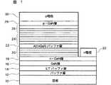
図1は、実施形態にかかるLEDの構成図である。
図2は、図1における発光層の詳細構成図である。
図3は、バリア層中に流すTMAの流量と出力パワーとの関係を示すグラフ図である。
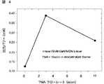
図4は、バッファ層中に流すTMAの流量と出力パワーとの関係を示すグラフ図である。
FIG. 2 is a detailed configuration diagram of the light emitting layer in FIG.
FIG. 3 is a graph showing the relationship between the flow rate of TMA flowing in the barrier layer and the output power.
FIG. 4 is a graph showing the relationship between the flow rate of TMA flowing in the buffer layer and the output power.
以下、図面に基づき本発明の実施形態について、半導体装置として発光素子、特にLEDを例にとり説明する。
図1には、本実施形態におけるLEDの構成が示されている。サファイアなどの基板10上に順次、SiNバッファ層12、低温(LT)成長バッファ層14、アンドープGaN層16が形成される。これらは、転位を低減するための層である。アンドープGaN層16上に動作電圧を低くするためのn−GaN層18が形成される。n−GaN層18上に、n−クラッド層20としてGaNとAlGaNを交互に積層した(n−GaN/n−AlGaN)のSLS(Strained Layer Superlattice:歪み超格子)層が形成される。そして、n−クラッド層20上に、AlInGaNバッファ層22及び発光層24が形成される。発光層24は後述のごとく、InGaN井戸層とAlInGaNバリア層を積層した多層量子井戸MQWからなる。発光層24上にp−クラッド層26としてGaNとAlGaNを積層した(p−GaN/p−AlGaN)のSLS層が形成される。すなわち、本実施形態のLEDは、AlInGaNバッファ層22とMQW発光層24をn−クラッド層20及びp−クラッド層26で挟んだ構成である。p−クラッド層26上に動作電圧を低くするためのp−GaN層28が形成され、さらにp−GaN層28上にp電極30が形成される。一方、n−GaN層18の一部を露出させ、その上にn電極32が形成される。各層は、MOCVD装置を用い、MOCVD法で成長される。
従来においては、発光層24としてInGaN等が用いられているが、本実施形態においては発光層24としてInGaN井戸層とAlInGaNバリア層を交互に積層した多層量子井戸MQWが用いられており、さらに発光層24をn−クラッド層20及びp−クラッド層26で挟む際に、発光層24に隣接させてAlInGaNバッファ層22が形成されている。
以下、発光層24及びバッファ層22について説明する。
図2には、図1における発光層24の構成が示されている。発光層24は、InGaN井戸層24bとAlxInyGa1−x−yNバリア層24aを交互に積層して構成される。ここで、0<x<1、0<y<1である。InGaN井戸層24bの厚さは例えば1.5nmであり、AlInGaNバリア層24aの厚さは例えば12nmである。繰り返し数は例えば7ペア(14層)である。AlInGaNバリア層24aのバンドギャップはInGaN井戸層24bのバンドギャップよりも広い。p電極30及びn電極32に順方向バイアスを印加すると、InGaN井戸層24bにて電子と正孔が結合して発光する。InGaN単層では原理的に波長363nm以下での発光は不可能であるが、井戸層とバリア層を交互に積層したMQWとすることで、InGaN井戸層24bの実効的バンドギャップが拡大される。実効バンドギャップの拡大により、波長363nm以下での発光が可能となる。発光領域であるInGaN井戸層24bはIn組成が比較的大きく(例えば、In組成x=10%)、In組成揺らぎも大きいため発光効率が高い。すなわち、組成に空間的な揺らぎがあるとキャリアの局在化が起こり、たとえInGaN内に転位が生じていても発光効率は低下しにくい。
また、AlxInyGa1−x−yNバリア層24aもInを含むため(y>0)、Inの組成揺らぎが生じ、井戸層24bと同様の理由でキャリアの局在化が生じ転位の存在によらず発光効率の低下が抑制される。バリア層24aとしてInを含まないAlGaNバリア層を用いた場合と比較すると、AlInGaNではInGaN井戸層24bとの格子不整合が小さく、格子不整合転位が生じにくく結晶性が高いというメリットがある。また、転位が発生しない場合であっても、AlInGaNでは井戸層24bとバリア層24aに生じる歪みが小さくなる。これらの層をc面成長させ、面内に圧縮あるいは引張応力が印加された場合、六方晶窒化物半導体は圧電性によりc軸方向に電界が発生する。この電界は、井戸層24b中に注入された電子正孔対を逆方向に移動させ、それらの波動関数の空間重なりを小さくして再結合率を小さくしてしまう。すなわち、井戸層24bに歪みがあると発光効率は低下する。このような効果(量子閉じ込めシュタルク効果)は、特に井戸層24bが広い場合に顕著に生じるが、井戸層24bが狭い場合であっても多少の影響はあり得る。本実施形態においては、バリア層24aとしてAlInGaNを用いて格子不整合を小さくし、井戸層24bの歪みを抑制しているため、量子閉じこめシュタルク効果による発光効率の低下も抑制される。
このように、発光層24においてInGaN井戸層24bを薄く、AlInGaNバリア層24aのバンドギャップを広くすることで、量子効果によりInGaN井戸層24bの実効的なバンドギャップを広げて発光波長360nm以下を達成できる。この点で、例えばInGaNではなくAlInGaNを発光層として用いる波長380nm以下のLEDと本質的に異なる。
InGaNを発光層とするLEDの場合、InGaN層の厚さが2nm以下になると発光効率が低下してしまう。これは、井戸層に閉じ込められた電子と正孔の波動関数がバリアの中(井戸の外)に滲み出し、バリア中での再結合の寄与が大きくなってしまうためである。本実施形態でも量子効果を生じさせるためにInGaN井戸層24bは2nm以下(例えば1.5nm)と薄くすることが必要であるが、本実施形態の発光層24はInGaN薄膜を発光層とした場合に生じる発光効率の低下は生じない。その理由は、バリア層24aとしてAlInGaNを用いているため、上述したようにInGaN井戸層24bのバンドギャップが実効的に拡大し、波動関数のバリア層24aへの滲み出しが小さくなっているためである。
なお、バリア層24aであるAlInGaNはAlを含むためにその成長温度はInGaNの成長温度(650℃〜750℃)より高い温度(例えば800℃)とする必要がある。このように750℃以上の温度で成長させることで、バリア層24aの結晶性も高くなる。
一方、バッファ層22はAlInGaNで構成される。バッファ層22はAlを含むため、バンドギャップが広くなり、InGaNである井戸層24bよりも広くなる。この層22により井戸層24bへの電子の注入効率が向上し、逆に正孔がバッファ層22に流れこむ量を小さくして、電子・正孔を効率的に井戸層24b内に閉じ込める。バッファ層22のAl組成は、例えば40%程度に設定できる。
以下、図1及び図2に示されたLEDの製造方法について具体的に説明する。本実施形態のLEDは以下のプロセスを経て製造される。すなわち、常圧MOCVD装置にて、サファイアc面基板10を反応管内のサセプタに載置し、1100℃にて水素雰囲気中で10分間熱処理する。その後、温度を500℃まで下げる。モノメチルシランガスとアンモニアガスをガス導入管から100秒間流し、基板10上に不連続的に(或いは島状に)SiNバッファ層12を成長させる。次に、同じ温度で厚さ25nmのGaNバッファ層(LTバッファ層)14をトリメチルガリウム及びアンモニアガスをガス導入管から供給して成長させる。そして、温度を1075℃まで上げ、再びトリメチルガリウム及びアンモニアガスを供給して厚さ2μmのアンドープGaN層16を成長させ、次にモノメチルシランガスを加えたSiドープのn−GaN層(n電極層)18を1.0μm成長させる。n−GaN層18中のキャリア密度はおよそ5×1018cm−3である。
次に、同一温度でSiドープのn−Al0.1Ga0.9N(2nm)/Siドープのn−GaN(2nm)を50ペア成長させてSLS構造としn−クラッド層20を成長させる。Alの原料としてはトリメチルアルミニウム(TMA)が用いられる。n−クラッド層20の平均電子密度は5×1018cm−3である。その後、温度を800℃程度まで下げてアンドープAl0.05In0.01Ga0.94Nバッファ層22を成長させる。バッファ層22の厚さは36nmである。成長温度が800℃と低いため、その抵抗率は高くなる。AlInGaNバッファ層22を成長させた後、同じ800℃でアンドープIn0.1Ga0.9N(1.5nm)/アンドープAl0.2In0.1Ga0.7N(95nm)を7ペア成長させてMQW発光層24を成長させる。発光層24の合計厚さは95nmである。
その後、温度を975℃まで上げてMgドープのp−Al0.1Ga0.9N(2nm)/Mgドープのp−GaN(1nm)を50周期成長させてSLS構造のp−クラッド層26を成長させ、さらに厚さ20nmのp−GaN層(p電極層)28を成長させる。SLSのp−クラッド層26及びp−GaN層28中の正孔濃度はそれぞれ5×1017cm−3、3×1018cm−3である。
表1に、各層の構造、組成、膜厚、成長温度を示す。
以上のようにして各層を順次成長させた後、ウエハをMOCVD装置から取り出し、Ni(10nm)、Au(10nm)を順次真空蒸着して表面に形成し、5%の酸素を含む窒素ガス雰囲気中、520℃で熱処理して蒸着金属膜をp透明電極30とする。その後、全面にフォオトレジストを塗布し、n電極形成のためのエッチングをフォトレジストをマスクとして用いる。エッチングにより露出したn−GaN層18上にTi(5nm)、Al(5nm)を真空蒸着し、窒素ガス中、450℃で30分間熱処理してn電極32を形成する。p電極30及びn電極32の一部にワイヤボンディング用の厚さ500nmの金パッドを形成し、基板10の裏面を100μmまで研磨してスクラブによりチップを切り出し、マウントしてLEDデバイスが得られる。
以上のようにして作成されたLEDデバイスを積分球の中に入れ、電流を注入してLEDデバイスから出射した全光出力を測定した。光出力は注入電流20mA時におよそ1.6mWであった。発光波長は、2インチ直径のウエハ面内で多少のばらつきはあるものの、360nm±5nmの範囲であった。
次に、発光層24におけるAlInGaNバリア層24aのバンドギャップの影響を確認すべく、バリア層24aの成長中に流す各種ガスのうち、TMA(トリメチルアルミニウム)の流量のみを変化させてLEDデバイスを作成し、作成したLEDの発光効率を調べた。
図3にその結果が示されている。横軸はバリア層24a成長中のTMA流量(フローレート:sccm)であり、容器に流し込むガスの流量を相対値で示したものである。縦軸は発光強度の相対値で、積分球を使って測定した値のおよそ1/4である。TMA流量を7sccmから10sccmに増加させると、発光効率は2.6倍になる。この状態で成長させたバリア層24aの組成は、In組成比が約1%、Al組成比が約20%である。Al組成比はTMA流量にほぼ比例するため、バリア層24aのAl組成比は14%(20×7sccm/10sccm)より大きいことが発光効率の観点から望ましい。一方、あまりにAl組成比が大きいと電流注入が行われにくくなり、動作電圧も高くなる。したがって、バリア層24aのAl組成比はその下限が発光効率から規定され、上限は動作電圧から規定されることとなり、具体的には14%以上40%以下が望ましく、16%以上40%以下がより望ましい。
また、バリア層24aのIn組成比については、In組成比が増大するとともにバンドギャップが狭くなるので、In組成比は小さい方が望ましいが、In組成比がゼロの場合には発光効率が激減する。これは、In組成揺らぎがバリア層24a中で生じ、発光効率改善に寄与しているためと考えられる。したがって、バリア層24aのIn組成比はその下限が組成揺らぎ量から規定され、上限がバンドギャップから規定されることとなり、具体的には0.1%以上5%以下が望ましく、0.1%以上3%以下がより望ましい。バリア層24aの組成の一例は、Alの組成比を40%、Inの組成比を1%としたAl0.4In0.01Ga0.59Nである。
一方、井戸層24bのIn組成比は、小さすぎるとIn組成揺らぎが小さくなって発光効率が低下し、In組成比が大きすぎると発光波長が長波長側にシフトしてしまう。したがって、最適なIn組成比は要求される発光波長と井戸層24bの厚さに依存して決定される。例えば、発光波長が360nmの場合には、5%以上15%以下が望ましく、5%以上13%以下がより望ましい。井戸層24bの組成の一例は、Inの組成比を5%としたIn0.05Ga0.95Nである。厚さに関しては、量子効果を出現させるべく1nm以上2nm以下が望ましく、1.3nm以上1.8nm以下がより望ましい。井戸層24bの厚さを3nm以上とすると、発光波長は400nmとなることを確認している。井戸層24b及びバリア層24aの成長温度は、上述したように750℃以上が望ましく、770℃以上(例えば800℃)がより望ましい。
次に、発光層24におけるバリア層24aの成長中に流すTMAの流量を10sccmに固定し、AlInGaNバッファ層22成長中に流すTMAを変化させて発光効率の変化を測定した。
図4にその結果が示されている。図において、横軸はTMA流量(フローレート)であり相対値である。縦軸は出力パワーの相対値である。TMA流量を増大させるとバッファ層22におけるAl組成比が増大する。TMA流量をゼロから3sccmに増加すると発光強度が2.7倍になる。さらにTMA流量を10sccmまで増加すると発光強度は逆に低下する。TMAがゼロの場合に発光強度が弱いのは、バッファ層22のバンドギャップが狭いため(Al組成比が0であるため)電子がバッファ層22から発光層24に有効に注入されないため、あるいは正孔がバッファ層22中に流れ出して正孔の井戸層24b中の閉じこめが不十分であるため、と考えられる。一方、Al組成比が大きすぎると発光効率が低下するのは、結晶性が低下するため、及びこの層のバンドギャップが広くなり過ぎ、n−クラッド層20から電子が注入されにくくなるためと考えられる。
したがって、AlInGaNバッファ層22のAl組成比は0.5%以上400%以下が望ましく、1%以上40%以下がより望ましい。AlInGaNバッファ層22のIn組成比については、In組成比がゼロの場合に発光効率が激減することを確認している。これは、In組成の揺らぎがバッファ層22内で起き、発光効率の改善に寄与しているためと考えられる。したがって、AlInGaNバッファ層22のIn組成比は0.1%以上5%以下が望ましく、0.1%以上3%以下がより望ましい。AlInGaNバッファ層22の組成の一例は、Al組成比を40%、In組成比を1%としたAl0.4In0.01Ga0.59Nである。
このように、本実施形態では、発光層24として所定の組成範囲のInGaN井戸とAlInGaNバリア層を交互に積層してなる多層量子井戸構造を用いてInGaNの実効的バンドギャップを拡大して340nm〜375nmの発光を可能とし、また、バリア層としてAlInGaNを用いることで発光効率を向上させ、さらに発光層に隣接して所定の組成範囲のAlInGaNバッファ層22を設けることでキャリアを効率的に注入して発光効率を向上させることができる。
以上、本発明の実施形態について説明したが、本発明はこれに限定されるものではなく種々の変更が可能である。
例えば、本実施形態ではSiNバッファ層12を形成しているが、転位を抑制するためのものであり、必要に応じてSiNバッファ層12を形成しなくてもよい。
また、SiNバッファ層12と低温(LT)成長バッファ層14を低温成長のGaNPバッファ層で置き換えることも可能である。Hereinafter, embodiments of the present invention will be described with reference to the drawings, taking a light-emitting element, particularly an LED, as a semiconductor device.
FIG. 1 shows the configuration of the LED in this embodiment. A
Conventionally, InGaN or the like is used as the
Hereinafter, the
FIG. 2 shows the configuration of the
Further, since the Alx Iny Ga1-xy
As described above, by thinning the InGaN
In the case of an LED having InGaN as a light emitting layer, the light emission efficiency is reduced when the thickness of the InGaN layer is 2 nm or less. This is because the wave function of electrons and holes confined in the well layer oozes out into the barrier (outside the well) and the contribution of recombination in the barrier increases. In this embodiment as well, the
Since AlInGaN as the
On the other hand, the
Hereinafter, a method for manufacturing the LED shown in FIGS. 1 and 2 will be described in detail. The LED of this embodiment is manufactured through the following process. That is, the sapphire c-
Next, 50 pairs of Si-doped n-Al0.1 Ga0.9 N (2 nm) / Si-doped n-GaN (2 nm) are grown at the same temperature to form an SLS structure, and the n-
Thereafter, the temperature is raised to 975 ° C., and 50 cycles of Mg-doped p-Al0.1 Ga0.9 N (2 nm) / Mg-doped p-GaN (1 nm) are grown to form a p-
Table 1 shows the structure, composition, film thickness, and growth temperature of each layer.
After each layer is grown sequentially as described above, the wafer is taken out of the MOCVD apparatus, and Ni (10 nm) and Au (10 nm) are sequentially vacuum-deposited to form on the surface, and in a nitrogen gas atmosphere containing 5% oxygen. The deposited metal film is made into the p
The LED device produced as described above was placed in an integrating sphere, and the total light output emitted from the LED device was measured by injecting current. The light output was approximately 1.6 mW at an injection current of 20 mA. The emission wavelength was in the range of 360 nm ± 5 nm, although there was some variation within the 2 inch diameter wafer surface.
Next, in order to confirm the influence of the band gap of the
The result is shown in FIG. The horizontal axis represents the TMA flow rate during the growth of the
As for the In composition ratio of the
On the other hand, if the In composition ratio of the
Next, the flow rate of TMA flowing during the growth of the
The result is shown in FIG. In the figure, the horizontal axis represents the TMA flow rate (flow rate), which is a relative value. The vertical axis represents the relative value of output power. When the TMA flow rate is increased, the Al composition ratio in the
Therefore, the Al composition ratio of the
As described above, in this embodiment, the effective band gap of InGaN is increased by using a multilayer quantum well structure in which InGaN wells and AlInGaN barrier layers having a predetermined composition range are alternately stacked as the
As mentioned above, although embodiment of this invention was described, this invention is not limited to this, A various change is possible.
For example, although the
It is also possible to replace the
Claims (4)
Translated fromJapanese前記発光層は、InGaN井戸層とAlInGaNバリア層を積層した多層量子井戸層を含み、
前記InGaN井戸層のIn組成比は5%以上15%以下であり、
前記InGaN井戸層の厚さは1nm以上2nm以下であり、
前記AlInGaNバリア層のAl組成比は14%以上40%以下であり、In組成比は0.1%以上5%以下である
ことを特徴とする窒化ガリウム系化合物半導体装置。A gallium nitride compound semiconductor devicethat emits ultraviolet light having awavelength of 375 nm or less, having a GaN-based light emitting layer formed on a substrate,
The light-emitting layerviewed including the multiple quantum well layer was laminated InGaN well layer and the AlInGaN barrierlayer,
The In composition ratio of the InGaN well layer is 5% or more and 15% or less,
The InGaN well layer has a thickness of 1 nm to 2 nm,
The Al composition ratio of the AlInGaN barrier layer is 14% or more and 40% or less, and the In composition ratio is 0.1% or more and 5% or less .
前記発光層に隣接したAlInGaNバッファ層
を有することを特徴とする窒化ガリウム系化合物半導体装置。The apparatus of claim 1, further comprising:
A gallium nitride-based compound semiconductor device havingan AlInGaN buffer layer adjacent to the light emitting layer .
前記AlInGaNバッファ層のAl組成比は0.5%以上40%以下であり、In組成比は0.1%以上5%以下であることを特徴とする窒化ガリウム系化合物半導体装置。The apparatus of claim 2.
The Al composition ratio of the AlInGaN buffer layer is 0.5% or more and 40% or less, and the In composition ratio is 0.1% or more and 5% or less .
前記InGaN井戸層及びAlInGaNバリア層は、750℃以上で形成されたものであることを特徴とする窒化ガリウム系化合物半導体装置。The apparatus of claim 1.
The GaN-based compound semiconductor device,wherein the InGaN well layer and the AlInGaN barrier layer are formed at 750 ° C. or higher .
Applications Claiming Priority (3)
| Application Number | Priority Date | Filing Date | Title |
|---|---|---|---|
| JP2002206581 | 2002-07-16 | ||
| JP2002206581 | 2002-07-16 | ||
| PCT/JP2003/008365WO2004008551A1 (en) | 2002-07-16 | 2003-07-01 | Gallium nitride-based compound semiconductor device |
Publications (2)
| Publication Number | Publication Date |
|---|---|
| JPWO2004008551A1 JPWO2004008551A1 (en) | 2005-11-17 |
| JP4234101B2true JP4234101B2 (en) | 2009-03-04 |
Family
ID=30112801
Family Applications (1)
| Application Number | Title | Priority Date | Filing Date |
|---|---|---|---|
| JP2004521142AExpired - LifetimeJP4234101B2 (en) | 2002-07-16 | 2003-07-01 | Gallium nitride compound semiconductor device |
Country Status (7)
| Country | Link |
|---|---|
| US (1) | US7700940B2 (en) |
| EP (1) | EP1536486A4 (en) |
| JP (1) | JP4234101B2 (en) |
| KR (1) | KR101002271B1 (en) |
| CN (1) | CN100521260C (en) |
| TW (1) | TWI292629B (en) |
| WO (1) | WO2004008551A1 (en) |
Families Citing this family (50)
| Publication number | Priority date | Publication date | Assignee | Title |
|---|---|---|---|---|
| KR101034055B1 (en) | 2003-07-18 | 2011-05-12 | 엘지이노텍 주식회사 | Light emitting diodes and manufacturing method |
| RU2247444C1 (en)* | 2004-03-15 | 2005-02-27 | Закрытое акционерное общество "Инновационная фирма "ТЕТИС" | Heavy-power light-emitting diode |
| KR100513923B1 (en)* | 2004-08-13 | 2005-09-08 | 재단법인서울대학교산학협력재단 | Growth method of nitride semiconductor layer and light emitting device using the growth method |
| DE102005048196B4 (en) | 2005-07-29 | 2023-01-26 | OSRAM Opto Semiconductors Gesellschaft mit beschränkter Haftung | Radiation-emitting semiconductor chip |
| JP4997621B2 (en)* | 2005-09-05 | 2012-08-08 | パナソニック株式会社 | Semiconductor light emitting device and lighting device using the same |
| US7462884B2 (en)* | 2005-10-31 | 2008-12-09 | Nichia Corporation | Nitride semiconductor device |
| GB2432715A (en)* | 2005-11-25 | 2007-05-30 | Sharp Kk | Nitride semiconductor light emitting devices |
| CN1996625A (en)* | 2006-01-06 | 2007-07-11 | 大连路明科技集团有限公司 | GaN-based optoelectronic device and its fabrication method |
| JP2007201195A (en)* | 2006-01-26 | 2007-08-09 | Sumitomo Electric Ind Ltd | Nitride semiconductor light emitting device |
| RU2306634C1 (en)* | 2006-08-08 | 2007-09-20 | Закрытое Акционерное Общество "Светлана - Оптоэлектроника" | Light-emitting semiconductor heterostructure |
| KR100809228B1 (en)* | 2006-11-20 | 2008-03-05 | 삼성전기주식회사 | Nitride Semiconductor Light Emitting Device |
| KR101459752B1 (en)* | 2007-06-22 | 2014-11-13 | 엘지이노텍 주식회사 | Semiconductor light emitting device and manufacturing method thereof |
| KR101122184B1 (en)* | 2007-08-14 | 2012-03-20 | 니텍 인코포레이티드 | Micro-pixel ultraviolet light emitting diode |
| KR101438808B1 (en)* | 2007-10-08 | 2014-09-05 | 엘지이노텍 주식회사 | Semiconductor light emitting device and fabrication method thereof |
| KR101459763B1 (en)* | 2008-01-15 | 2014-11-12 | 엘지이노텍 주식회사 | Semiconductor light emitting device and manufacturing method thereof |
| DE102008028036A1 (en)* | 2008-02-29 | 2009-09-03 | Osram Opto Semiconductors Gmbh | Optoelectronic semiconductor body with tunnel junction and method for producing such |
| EP2325899A4 (en)* | 2008-08-29 | 2015-04-29 | Toshiba Kk | SEMICONDUCTOR DEVICE |
| WO2010100942A1 (en)* | 2009-03-05 | 2010-09-10 | 株式会社小糸製作所 | Light-emitting module, method of producing light-emitting module, and lighting unit |
| CN101521258B (en)* | 2009-03-27 | 2013-07-31 | 华灿光电股份有限公司 | Method for improving LED external quantum efficiency |
| JP5306254B2 (en)* | 2010-02-12 | 2013-10-02 | 株式会社東芝 | Semiconductor light emitting device |
| US8907322B2 (en) | 2010-06-18 | 2014-12-09 | Sensor Electronic Technology, Inc. | Deep ultraviolet light emitting diode |
| US9806226B2 (en) | 2010-06-18 | 2017-10-31 | Sensor Electronic Technology, Inc. | Deep ultraviolet light emitting diode |
| US8927959B2 (en) | 2010-06-18 | 2015-01-06 | Sensor Electronic Technology, Inc. | Deep ultraviolet light emitting diode |
| US8362458B2 (en) | 2010-12-27 | 2013-01-29 | Industrial Technology Research Institute | Nitirde semiconductor light emitting diode |
| CN102097555A (en)* | 2011-01-14 | 2011-06-15 | 武汉迪源光电科技有限公司 | Epitaxial structure of diode |
| US8358673B2 (en)* | 2011-02-17 | 2013-01-22 | Corning Incorporated | Strain balanced laser diode |
| JP2013008803A (en)* | 2011-06-23 | 2013-01-10 | Toyoda Gosei Co Ltd | Method for manufacturing group iii nitride semiconductor light-emitting element |
| EP2745326A1 (en) | 2011-08-17 | 2014-06-25 | Ramgoss Inc. | Vertical field effect transistor on oxide semiconductor substrate and method of manufacturing the same |
| JP2013106550A (en)* | 2011-11-18 | 2013-06-06 | Sharp Corp | Lighting device for growing plant |
| CN103137824A (en)* | 2011-11-29 | 2013-06-05 | 昆山开威电子有限公司 | White light light-emitting diode device and encapsulation method without gold thread |
| JP5874593B2 (en)* | 2011-12-23 | 2016-03-02 | 豊田合成株式会社 | Group III nitride semiconductor light emitting device and method for manufacturing the same |
| US8927984B2 (en) | 2012-01-17 | 2015-01-06 | Ramgoss, Inc. | Rotated channel semiconductor field effect transistor |
| CN102544281A (en)* | 2012-01-20 | 2012-07-04 | 厦门市三安光电科技有限公司 | Gallium nitride-based LED with multi-layer potential barrier structure |
| DE102012104671B4 (en) | 2012-05-30 | 2020-03-05 | Osram Opto Semiconductors Gmbh | Method for producing an active zone for an optoelectronic semiconductor chip |
| KR101961303B1 (en)* | 2012-05-30 | 2019-03-25 | 엘지이노텍 주식회사 | Light emitting device package and light emitting system |
| JP6001446B2 (en) | 2012-12-28 | 2016-10-05 | 株式会社東芝 | Semiconductor light emitting device and manufacturing method thereof |
| US20150280057A1 (en)* | 2013-03-15 | 2015-10-01 | James R. Grandusky | Methods of forming planar contacts to pseudomorphic electronic and optoelectronic devices |
| WO2014168339A1 (en) | 2013-04-12 | 2014-10-16 | 서울바이오시스 주식회사 | Ultraviolet light-emitting device |
| US9112077B1 (en) | 2014-04-28 | 2015-08-18 | Industrial Technology Research Institute | Semiconductor structure |
| KR102212561B1 (en)* | 2014-08-11 | 2021-02-08 | 삼성전자주식회사 | Semiconductor light emitting device and semiconductor light emitting device package |
| TWI568016B (en)* | 2014-12-23 | 2017-01-21 | 錼創科技股份有限公司 | Semiconductor light-emitting element |
| KR102322692B1 (en) | 2015-05-29 | 2021-11-05 | 쑤저우 레킨 세미컨덕터 컴퍼니 리미티드 | Ultraviolet light emitting device |
| CN106571416B (en)* | 2016-11-04 | 2019-09-10 | 华灿光电(浙江)有限公司 | Light emitting diode epitaxial wafer and manufacturing method thereof |
| US10141477B1 (en)* | 2017-07-28 | 2018-11-27 | Lumileds Llc | Strained AlGaInP layers for efficient electron and hole blocking in light emitting devices |
| US11322650B2 (en) | 2017-07-28 | 2022-05-03 | Lumileds Llc | Strained AlGaInP layers for efficient electron and hole blocking in light emitting devices |
| FR3091005B1 (en)* | 2018-12-21 | 2021-01-29 | Soitec Silicon On Insulator | GROWTH SUBSTRATE AND MANUFACTURING PROCESS OF SUCH SUBSTRATE |
| CN109830578B (en)* | 2019-02-18 | 2020-06-09 | 湘能华磊光电股份有限公司 | Growth method of LED epitaxial structure |
| CN113451459B (en)* | 2020-11-02 | 2022-05-13 | 重庆康佳光电技术研究院有限公司 | Light emitting diode, epitaxial structure and method of making the same |
| CN113451455B (en)* | 2020-11-26 | 2022-05-03 | 重庆康佳光电技术研究院有限公司 | LED epitaxy preparation method, LED epitaxy structure and LED chip |
| JP7488410B1 (en) | 2023-05-09 | 2024-05-21 | 日機装株式会社 | Method and device for predicting light output of nitride semiconductor light emitting device |
Family Cites Families (18)
| Publication number | Priority date | Publication date | Assignee | Title |
|---|---|---|---|---|
| US1051074A (en)* | 1911-04-25 | 1913-01-21 | Sheridan Iron Works | Bookbinding-machine. |
| US4992837A (en)* | 1988-11-15 | 1991-02-12 | Kokusai Denshin Denwa Co., Ltd. | Light emitting semiconductor device |
| SE501635C2 (en)* | 1993-08-20 | 1995-04-03 | Asea Brown Boveri | Method and apparatus for transmitting light with integrated excitation source |
| US5684309A (en)* | 1996-07-11 | 1997-11-04 | North Carolina State University | Stacked quantum well aluminum indium gallium nitride light emitting diodes |
| JP3716395B2 (en) | 1996-08-02 | 2005-11-16 | 富士通株式会社 | Semiconductor light emitting device |
| JPH10270756A (en) | 1997-03-27 | 1998-10-09 | Sanyo Electric Co Ltd | Gallium nitride compound semiconductor device |
| JPH10303458A (en)* | 1997-04-24 | 1998-11-13 | Toyoda Gosei Co Ltd | Gallium nitride compound semiconductor element |
| JPH11243251A (en) | 1998-02-26 | 1999-09-07 | Toshiba Corp | Semiconductor laser device |
| JP3468082B2 (en) | 1998-02-26 | 2003-11-17 | 日亜化学工業株式会社 | Nitride semiconductor device |
| JP3519990B2 (en) | 1998-12-09 | 2004-04-19 | 三洋電機株式会社 | Light emitting device and manufacturing method thereof |
| JP3487251B2 (en) | 1999-03-04 | 2004-01-13 | 日亜化学工業株式会社 | Nitride semiconductor laser device |
| JP3285341B2 (en) | 2000-06-01 | 2002-05-27 | 士郎 酒井 | Method of manufacturing gallium nitride based compound semiconductor |
| TW472400B (en)* | 2000-06-23 | 2002-01-11 | United Epitaxy Co Ltd | Method for roughing semiconductor device surface to increase the external quantum efficiency |
| US6800876B2 (en)* | 2001-01-16 | 2004-10-05 | Cree, Inc. | Group III nitride LED with undoped cladding layer (5000.137) |
| US6489636B1 (en)* | 2001-03-29 | 2002-12-03 | Lumileds Lighting U.S., Llc | Indium gallium nitride smoothing structures for III-nitride devices |
| JP3645233B2 (en)* | 2001-06-07 | 2005-05-11 | 日本電信電話株式会社 | Semiconductor element |
| US6822272B2 (en)* | 2001-07-09 | 2004-11-23 | Nichia Corporation | Multilayered reflective membrane and gallium nitride-based light emitting element |
| TWI271877B (en)* | 2002-06-04 | 2007-01-21 | Nitride Semiconductors Co Ltd | Gallium nitride compound semiconductor device and manufacturing method |
- 2003
- 2003-07-01JPJP2004521142Apatent/JP4234101B2/ennot_activeExpired - Lifetime
- 2003-07-01KRKR1020057000163Apatent/KR101002271B1/ennot_activeExpired - Lifetime
- 2003-07-01USUS10/521,544patent/US7700940B2/ennot_activeExpired - Lifetime
- 2003-07-01CNCNB038168731Apatent/CN100521260C/ennot_activeExpired - Lifetime
- 2003-07-01EPEP03738612Apatent/EP1536486A4/ennot_activeWithdrawn
- 2003-07-01WOPCT/JP2003/008365patent/WO2004008551A1/enactiveApplication Filing
- 2003-07-14TWTW092119118Apatent/TWI292629B/ennot_activeIP Right Cessation
Also Published As
| Publication number | Publication date |
|---|---|
| US20050236642A1 (en) | 2005-10-27 |
| EP1536486A1 (en) | 2005-06-01 |
| CN100521260C (en) | 2009-07-29 |
| EP1536486A4 (en) | 2006-11-08 |
| TWI292629B (en) | 2008-01-11 |
| CN1669158A (en) | 2005-09-14 |
| TW200405591A (en) | 2004-04-01 |
| JPWO2004008551A1 (en) | 2005-11-17 |
| WO2004008551A1 (en) | 2004-01-22 |
| US7700940B2 (en) | 2010-04-20 |
| KR20050026473A (en) | 2005-03-15 |
| KR101002271B1 (en) | 2010-12-20 |
Similar Documents
| Publication | Publication Date | Title |
|---|---|---|
| JP4234101B2 (en) | Gallium nitride compound semiconductor device | |
| JP3863177B2 (en) | Gallium nitride light emitting device | |
| JP5549338B2 (en) | Nitrogen compound semiconductor LED for ultraviolet light radiation and method for producing the same | |
| CN101188264B (en) | Nitride semiconductor light emitting device | |
| JPH10290027A (en) | Semiconductor light emitting device and method of manufacturing the same | |
| JP2008118049A (en) | GaN-BASED SEMICONDUCTOR LIGHT EMITTING DEVICE | |
| Mukai et al. | Nitride light-emitting diodes | |
| CN102810607B (en) | For the manufacture of the method for III group nitride compound semiconductor light emitting element | |
| JP3951973B2 (en) | Nitride semiconductor device | |
| JP2008288532A (en) | Nitride semiconductor device | |
| JP2017017265A (en) | Light-emitting device | |
| JP3434162B2 (en) | Nitride semiconductor device | |
| JP2003086840A (en) | GaN-BASED SEMICONDUCTOR LIGHT EMITTING DIODE | |
| JP5258507B2 (en) | Method for manufacturing gallium nitride based light emitting device | |
| JPH10144960A (en) | Method for manufacturing p-type nitride semiconductor and nitride semiconductor device | |
| KR100643262B1 (en) | Gallium Nitride Light Emitting Device | |
| JP2008118048A (en) | GaN-BASED SEMICONDUCTOR LIGHT EMITTING DEVICE | |
| JP2009026865A (en) | Manufacturing method of group iii nitride-based compound semiconductor light emitting element | |
| JP3857417B2 (en) | Nitride semiconductor device | |
| JP2005311119A (en) | Gallium nitride-based light emitting device | |
| JP2005317823A (en) | Gallium nitride system light emitting device | |
| JP2007201145A (en) | Growing method of n-type group iii nitride compound semiconductor layer | |
| JP2002151798A (en) | Nitride semiconductor device | |
| JP2004247682A (en) | Semiconductor multilayer structure and semiconductor device equipped with that structure | |
| JP2000294829A (en) | Semiconductor laminated structure, semiconductor device having the same and crystal growth method |
Legal Events
| Date | Code | Title | Description |
|---|---|---|---|
| A621 | Written request for application examination | Free format text:JAPANESE INTERMEDIATE CODE: A621 Effective date:20060622 | |
| A131 | Notification of reasons for refusal | Free format text:JAPANESE INTERMEDIATE CODE: A131 Effective date:20080708 | |
| A521 | Request for written amendment filed | Free format text:JAPANESE INTERMEDIATE CODE: A523 Effective date:20080902 | |
| TRDD | Decision of grant or rejection written | ||
| A01 | Written decision to grant a patent or to grant a registration (utility model) | Free format text:JAPANESE INTERMEDIATE CODE: A01 Effective date:20081111 | |
| A01 | Written decision to grant a patent or to grant a registration (utility model) | Free format text:JAPANESE INTERMEDIATE CODE: A01 | |
| A61 | First payment of annual fees (during grant procedure) | Free format text:JAPANESE INTERMEDIATE CODE: A61 Effective date:20081210 | |
| FPAY | Renewal fee payment (event date is renewal date of database) | Free format text:PAYMENT UNTIL: 20111219 Year of fee payment:3 | |
| R150 | Certificate of patent or registration of utility model | Ref document number:4234101 Country of ref document:JP Free format text:JAPANESE INTERMEDIATE CODE: R150 Free format text:JAPANESE INTERMEDIATE CODE: R150 | |
| FPAY | Renewal fee payment (event date is renewal date of database) | Free format text:PAYMENT UNTIL: 20141219 Year of fee payment:6 | |
| R250 | Receipt of annual fees | Free format text:JAPANESE INTERMEDIATE CODE: R250 | |
| R250 | Receipt of annual fees | Free format text:JAPANESE INTERMEDIATE CODE: R250 | |
| R250 | Receipt of annual fees | Free format text:JAPANESE INTERMEDIATE CODE: R250 | |
| R250 | Receipt of annual fees | Free format text:JAPANESE INTERMEDIATE CODE: R250 | |
| EXPY | Cancellation because of completion of term |