JP4233016B2 - Driving device for light emitting display panel - Google Patents
Driving device for light emitting display panelDownload PDFInfo
- Publication number
- JP4233016B2 JP4233016B2JP2002294706AJP2002294706AJP4233016B2JP 4233016 B2JP4233016 B2JP 4233016B2JP 2002294706 AJP2002294706 AJP 2002294706AJP 2002294706 AJP2002294706 AJP 2002294706AJP 4233016 B2JP4233016 B2JP 4233016B2
- Authority
- JP
- Japan
- Prior art keywords
- tft
- light
- voltage
- driving
- gate
- Prior art date
- Legal status (The legal status is an assumption and is not a legal conclusion. Google has not performed a legal analysis and makes no representation as to the accuracy of the status listed.)
- Expired - Fee Related
Links
Images


Landscapes
- Electroluminescent Light Sources (AREA)
- Control Of Indicators Other Than Cathode Ray Tubes (AREA)
- Control Of El Displays (AREA)
Description
Translated fromJapanese【0001】
【発明の属する技術分野】
この発明は、画素を構成する発光素子をTFT(Thin Film Transistor)によってアクティブ駆動させる発光表示パネルの駆動装置に関し、特に発光表示パネルを駆動するに要する電源回路における電源電圧の数を低減させることができる発光表示パネルの駆動装置に関する。
【0002】
【従来の技術】
発光素子をマトリクス状に配列して構成される表示パネルを用いたディスプレイの開発が広く進められている。このような表示パネルに用いられる発光素子として、有機材料を発光層に用いた有機EL(エレクトロルミネッセンス)素子が注目されている。これはEL素子の発光層に、良好な発光特性を期待することができる有機化合物を使用することによって、実用に耐えうる高効率化および長寿命化が進んだことも背景にある。
【0003】
かかる有機EL素子を用いた表示パネルとして、EL素子を単にマトリクス状に配列した単純マトリクス型表示パネルと、マトリクス状に配列したEL素子の各々に、TFTからなる能動素子を加えたアクティブマトリクス型表示パネルが提案されている。後者のアクティブマトリクス型表示パネルは、前者の単純マトリクス型表示パネルに比べて、低消費電力を実現することができ、また画素間のクロストークが少ない等の特質を備えており、特に大画面を構成する高精細度のディスプレイに適している。
【0004】
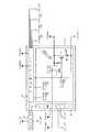
図1は、従来のアクティブマトリクス型表示パネルにおける1つの画素に対応する回路構成と、各画素を個別に点灯駆動するためのコントローラ並びにドライバー、およびこれらに駆動電力を供給する各電源電圧の供給形態を示したものである。また、図2も従来のアクティブマトリクス型表示パネルにおける他の構成例を示したものである。
【0005】
図1および図2に示すアクティブマトリクス型表示パネル1においては、表示画素が配列される透明基板上に、データドライバー2(以下、これをカラム側ドライバーとも言う。)、および走査ドライバー3(以下、これをロー側ドライバーとも言う。)を搭載し、外付けのコントローラ4との間で接続される信号線等の数を極力少なくする工夫がなされている。
【0006】
そして、1つの画素10に対応する回路構成は、発光素子としてのEL素子E1 と、前記EL素子E1 を点灯駆動する駆動用TFT(Tr1)と、前記駆動用TFTのゲート電圧を制御する制御用TFT(Tr2)と、前記駆動用TFTのゲート電圧を保持するコンデンサC1 より構成している。この図1および図2に示した画素10を構成する回路例は、コンダクタンスコントロール方式と称される最も基本的な例を示している。
【0007】
ここで、各回路の駆動用電源について考察した場合、図1および図2に示すようにコントローラ(外部ロジック回路)4、カラム側ドライバー2、およびロー側ドライバー3においては、各回路の駆動電圧源としてそれぞれに高レベル側と低レベル側の2つの電圧レベルが必要となる。また、駆動用TFT(Tr1)のオン/オフ制御、並びに制御用TFTのオン/オフ制御に、それぞれ2つの異なるレベルの制御信号電圧が必要となる。
【0008】
さらに、R(赤)、G(緑)、B(青)の各発光画素(サブピクセル)を備えたフルカラーの発光表示パネルを構成する場合においては、それぞれサブピクセルを構成するEL素子の発光効率の相異を是正するために、図1に示す例においては、R,G,Bに対応した異なる3つのレベルの陽極側電圧電源(VHanod)、および1つの陰極側電圧電源(VLcath)が必要になる。また、図2に示す例においては、前記した3つのレベルの陽極側電圧電源に代えて、同じくR,G,Bに対応した3つの異なったレベルのデータ電圧電源(VLdata)が必要になる。
【0009】
一方、前記した有機EL素子などの電流駆動型の発光素子をアクティブ駆動させるためには、相当の電子移動度が必要であるといわれており、これを駆動するために一般的にはポリシリコンTFTが使用されている。そして、駆動用のTFT(Tr1)においては、EL素子E1 の構造上の理由などから、Pチャンネル型を使用し、制御用TFT(Tr2)においては、小さい保持容量で所定の保持時間を確保するために、オフ時のリーク電流が小さいNチャンネル型を使用する構成が好ましいとされている(例えば非特許文献1参照)。
【0010】
【非特許文献1】
日経エレクトロニクス、2000年4月24日(No.768)
【0011】
【発明が解決しようとする課題】
ところで、駆動用のTFT(Tr1)にPチャンネル型を、また制御用TFT(Tr2)にNチャンネル型を使用した図1に示した例、および図2に示した例によると、それぞれ14の電源数が必要であることが判る。次に示す表1は図1に示す構成において使用される電源電圧の例をより具体的に示したものである。
【0012】
【表1】
前記図1に示した発光表示パネルの駆動装置によると、表1に示すような電源数を必要とすることになるが、特にこの種の発光表示パネルを携帯用機器へ搭載することを考えた場合には、実装スペースと消費電力の点から、電源電圧の数はできる限り少なくして、これらが共用できるようにすることが望まれる。そこで、電源を共用化して電源数を削減しようとした場合、次のような共用化を考えることができる。
【0014】
まず、各ドライバー2,3の電源に着目した場合、
VHcolu=VHrow
であるので、これを(VHdriv)として共用化することができる。同様に、
VLcolu=VLrow
であるので、これを(VLdriv)として共用化することができる。次に各TFT(Tr1,Tr2)の特性が、Vgs=0VでId =0Aであるとすると、すなわち、駆動用および制御用TFTのゲート電圧を0Vとした時に、TFTがカットオフ状態になるという特性のものを使用すれば、
VHdata=VHanod
としても、駆動用TFT(Tr1)をオフ状態に維持させることができる。これを(VHelem)として共用化することができる。同様に
VLcont=VLdata
としても、制御用TFT(Tr2)はVHdataおよびVLdataに対して、共にオフ状態を維持させることができる。さらに
VLcont=VLdata=VLdriv
としても、回路においては支障なく動作させることができる。したがって、これを前記した(VLdriv)として共用化することができる。
【0015】
一方、図1に示すコントローラ4を駆動させる外部ロジック電源は、一般的に3.3Vや2.8Vと低い電圧であり、これらの電圧ではTFTは動作できないなどの理由から、外部ロジック電源と、カラム側ドライバー2、ロー側ドライバー3の各電源を共用化することは不可能である。一般的に外部ロジック電源は、ドライバー電源が挟み込む次に示す電圧順位になされている。
VHdriv>VHlogi VLlogi>VLdriv
【0016】
また、VHcontは制御用TFT(Tr2)を介して、電荷保持用コンデンサC1 に対してVHdataが書き込まれる時、制御用TFT(Tr2)を完全にオン状態にするために、
VHdata<VHcont
の条件になされていることが必要である。以上のような考察に基づいて電源を共用化した例を図3に示しており、図1に示す構成においては、これ以上の電源数の削減は不可能であると言える。しかしながら、なおも電源数を低減させることは実装スペースと消費電力の点から好ましいことであることは前記したとおりである。
【0017】
この発明は前記したような観点に基づいてなされたものであり、以下に示すように、さらに電源数を低減させることができる発光表示パネルの駆動装置を提供することを技術的な課題とするものである。
【0018】
【課題を解決するための手段】
前記した課題を解決するためになされたこの発明にかかる発光表示パネルの駆動装置は、以下の各独立請求項にかかる構成を少なくとも具備するものである。
【0019】
請求項1にかかる発明の発光表示パネルの駆動装置は、
発光素子と、前記発光素子を点灯駆動する駆動用TFTと、前記駆動用TFTのゲート電圧を制御する制御用TFTとによる発光画素をマトリックス状に配列したアクティブマトリックス型発光表示パネルと、前記発光表示パネルの各発光画素を選択的に発光駆動するデータドライバーおよび走査ドライバーと、前記データドライバーおよび走査ドライバーに対して、映像データに基づく指令信号を与えるコントローラとを具備した発光表示パネルの駆動装置であって、
前記データドライバー、走査ドライバー、およびコントローラとが、少なくとも2つの異なるレベルの駆動電圧によって駆動動作がなされ、さらに前記データドライバーには前記駆動用TFTのゲートに加える少なくとも2つの異なるレベルの制御信号電圧が供給されると共に、前記走査ドライバーには前記制御用TFTのゲートに加える少なくとも2つの異なるレベルの制御信号電圧が供給されるように構成され、
前記データドライバーに加える低レベル側の駆動電圧(VLcolu)と、前記走査ドライバーに加える低レベル側の駆動電圧(VLrow)と、前記制御用TFTのゲートに加える低レベル側の制御信号電圧(VLcont)とを同一の電圧レベルで共用してVLdrivとし、また、前記コントローラに加える低レベル側の駆動電圧をVLlogiとし、
かつ、前記発光画素を構成する少なくとも前記駆動用TFTと制御用TFTとが、共にPチャンネルのTFTで構成され、また前記制御用TFTはエンハンストメント型のTFTで構成され、前記制御用TFTがオン状態となるゲート・ソース間電圧VgsをVonとした時、
【数33】
VLlogi−VLdriv≧−Von
【数34】
VLlogi>VLdriv
【数35】
VLcont=VLdriv
の条件を満足する電位関係になされており、
かつ前記発光素子に加える陽極側電圧(VHanod)または陰極側電圧(VLcath)で発光素子の輝度を調整する構成において、前記駆動用TFTのゲートに加える低レベル側の制御信号電圧をVLdataとした時、
【数36】
VLdata=VLlogi
の条件を満足する電位関係になされていることを特徴とする。
【0020】
請求項2にかかる発明の発光表示パネルの駆動装置は、
発光素子と、前記発光素子を点灯駆動する駆動用TFTと、前記駆動用TFTのゲート電圧を制御する制御用TFTとによる発光画素をマトリックス状に配列したアクティブマトリックス型発光表示パネルと、前記発光表示パネルの各発光画素を選択的に発光駆動するデータドライバーおよび走査ドライバーと、前記データドライバーおよび走査ドライバーに対して、映像データに基づく指令信号を与えるコントローラとを具備した発光表示パネルの駆動装置であって、
前記データドライバー、走査ドライバー、およびコントローラとが、少なくとも2つの異なるレベルの駆動電圧によって駆動動作がなされ、さらに前記データドライバーには前記駆動用TFTのゲートに加える少なくとも2つの異なるレベルの制御信号電圧が供給されると共に、前記走査ドライバーには前記制御用TFTのゲートに加える少なくとも2つの異なるレベルの制御信号電圧が供給されるように構成され、
前記データドライバーに加える低レベル側の駆動電圧(VLcolu)と、前記走査ドライバーに加える低レベル側の駆動電圧(VLrow)と、前記制御用TFTのゲートに加える低レベル側の制御信号電圧(VLcont)とを同一の電圧レベルで共用してVLdrivとし、また、前記コントローラに加える低レベル側の駆動電圧をVLlogiとし、
かつ、前記発光画素を構成する少なくとも前記駆動用TFTと制御用TFTとが、共にPチャンネルのTFTで構成され、また前記制御用TFTはエンハンストメント型のTFTで構成され、前記制御用TFTがオン状態となるゲート・ソース間電圧VgsをVonとした時、
【数37】
VLlogi−VLdriv≧−Von
【数38】
VLlogi>VLdriv
【数39】
VLcont=VLdriv
の条件を満足する電位関係になされており、
かつ前記駆動用TFTのゲートに加える低レベル側の制御信号電圧(VLdata)で発光素子の輝度を調整する構成において、
【数40】
VLdata≧VLlogi
の条件を満足する電位関係になされていることを特徴とする。
【0021】
請求項3にかかる発明の発光表示パネルの駆動装置は、
発光素子と、前記発光素子を点灯駆動する駆動用TFTと、前記駆動用TFTのゲート電圧を制御する制御用TFTとによる発光画素をマトリックス状に配列したアクティブマトリックス型発光表示パネルと、前記発光表示パネルの各発光画素を選択的に発光駆動するデータドライバーおよび走査ドライバーと、前記データドライバーおよび走査ドライバーに対して、映像データに基づく指令信号を与えるコントローラとを具備した発光表示パネルの駆動装置であって、
前記データドライバー、走査ドライバー、およびコントローラとが、少なくとも2つの異なるレベルの駆動電圧によって駆動動作がなされ、さらに前記データドライバーには前記駆動用TFTのゲートに加える少なくとも2つの異なるレベルの制御信号電圧が供給されると共に、前記走査ドライバーには前記制御用TFTのゲートに加える少なくとも2つの異なるレベルの制御信号電圧が供給されるように構成され、
前記データドライバーに加える低レベル側の駆動電圧(VLcolu)と、前記走査ドライバーに加える低レベル側の駆動電圧(VLrow)と、前記制御用TFTのゲートに加える低レベル側の制御信号電圧(VLcont)とを同一の電圧レベルで共用してVLdrivとし、また、前記コントローラに加える低レベル側の駆動電圧をVLlogiとし、
かつ、前記発光画素を構成する少なくとも前記駆動用TFTと制御用TFTとが、共にNチャンネルのTFTで構成され、また前記制御用TFTはエンハンストメント型のTFTで構成され、前記制御用TFTがオン状態となるゲート・ソース間電圧VgsをVonとした時、
【数41】
VLlogi−VLdriv≧Von
【数42】
VLlogi>VLdriv
の条件を満足し、前記制御用TFTのゲートに加える高レベル側の制御信号電圧を
VHcontとした時、
【数43】
VLlogi=VHcont
の条件を満足する電位関係になされており、
かつ前記発光素子に加える陽極側電圧(VHanod)または陰極側電圧(VLcath)で発光素子の輝度を調整する構成において、前記駆動用TFTのゲートに加える高レベル側の制御信号電圧をVHdataとした時、
【数44】
VLdriv=VHdata
の条件を満足する電位関係になされていることを特徴とする。
【0022】
請求項4にかかる発明の発光表示パネルの駆動装置は、
発光素子と、前記発光素子を点灯駆動する駆動用TFTと、前記駆動用TFTのゲート電圧を制御する制御用TFTとによる発光画素をマトリックス状に配列したアクティブマトリックス型発光表示パネルと、前記発光表示パネルの各発光画素を選択的に発光駆動するデータドライバーおよび走査ドライバーと、前記データドライバーおよび走査ドライバーに対して、映像データに基づく指令信号を与えるコントローラとを具備した発光表示パネルの駆動装置であって、
前記データドライバー、走査ドライバー、およびコントローラとが、少なくとも2つの異なるレベルの駆動電圧によって駆動動作がなされ、さらに前記データドライバーには前記駆動用TFTのゲートに加える少なくとも2つの異なるレベルの制御信号電圧が供給されると共に、前記走査ドライバーには前記制御用TFTのゲートに加える少なくとも2つの異なるレベルの制御信号電圧が供給されるように構成され、
前記データドライバーに加える低レベル側の駆動電圧(VLcolu)と、前記走査ドライバーに加える低レベル側の駆動電圧(VLrow)と、前記制御用TFTのゲートに加える低レベル側の制御信号電圧(VLcont)とを同一の電圧レベルで共用してVLdrivとし、また、前記コントローラに加える低レベル側の駆動電圧をVLlogiとし、
かつ、前記発光画素を構成する少なくとも前記駆動用TFTと制御用TFTとが、共にNチャンネルのTFTで構成され、また前記制御用TFTはエンハンストメント型のTFTで構成され、前記制御用TFTがオン状態となるゲート・ソース間電圧VgsをVonとした時、
【数45】
VLlogi−VLdriv≧Von
【数46】
VLlogi>VLdriv
の条件を満足し、前記制御用TFTのゲートに加える高レベル側の制御信号電圧を
VHcontとした時、
【数47】
VLlogi=VHcont
の条件を満足する電位関係になされており、
かつ前記駆動用TFTのゲートに加える高レベル側の制御信号電圧(VHdata)で発光素子の輝度を調整する構成において、
【数48】
VLdriv≧VHdata
の条件を満足する電位関係になされていることを特徴とする。
【0023】
請求項5にかかる発明の発光表示パネルの駆動装置は、
発光素子と、前記発光素子を点灯駆動する駆動用TFTと、前記駆動用TFTのゲート電圧を制御する制御用TFTとによる発光画素をマトリックス状に配列したアクティブマトリックス型発光表示パネルと、前記発光表示パネルの各発光画素を選択的に発光駆動するデータドライバーおよび走査ドライバーと、前記データドライバーおよび走査ドライバーに対して、映像データに基づく指令信号を与えるコントローラとを具備した発光表示パネルの駆動装置であって、
前記データドライバー、走査ドライバー、およびコントローラとが、少なくとも2つの異なるレベルの駆動電圧によって駆動動作がなされ、さらに前記データドライバーには前記駆動用TFTのゲートに加える少なくとも2つの異なるレベルの制御信号電圧が供給されると共に、前記走査ドライバーには前記制御用TFTのゲートに加える少なくとも2つの異なるレベルの制御信号電圧が供給されるように構成され、
前記データドライバーに加える低レベル側の駆動電圧(VLcolu)と、前記走査ドライバーに加える低レベル側の駆動電圧(VLrow)と、前記制御用TFTのゲートに加える低レベル側の制御信号電圧(VLcont)とを同一の電圧レベルで共用してVLdrivとし、また、前記コントローラ駆動用の低レベル側駆動電位をVLlogiとし、
かつ、前記発光画素を構成する少なくとも前記駆動用TFTがPチャンネル、制御用TFTがNチャンネルのTFTで構成され、また前記制御用TFTはデプレッション型のTFTで構成され、前記制御用TFTがオフ状態となるゲート・ソース間電圧VgsをVoffとした時、
【数49】
VLlogi−VLdriv≧−Voff
【数50】
VLlogi>VLdriv
【数51】
VLcont=VLdriv
の条件を満足する電位関係になされており、
かつ前記発光素子に加える陽極側電圧(VHanod)または陰極側電圧(VLcath)で発光素子の輝度を調整する構成において、前記駆動用TFTのゲートに加える低レベル側の制御信号電圧をVLdataとした時、
【数52】
VLdata=VLlogi
の条件を満足する電位関係になされていることを特徴とする。
【0024】
請求項6にかかる発明の発光表示パネルの駆動装置は、
発光素子と、前記発光素子を点灯駆動する駆動用TFTと、前記駆動用TFTのゲート電圧を制御する制御用TFTとによる発光画素をマトリックス状に配列したアクティブマトリックス型発光表示パネルと、前記発光表示パネルの各発光画素を選択的に発光駆動するデータドライバーおよび走査ドライバーと、前記データドライバーおよび走査ドライバーに対して、映像データに基づく指令信号を与えるコントローラとを具備した発光表示パネルの駆動装置であって、
前記データドライバー、走査ドライバー、およびコントローラとが、少なくとも2つの異なるレベルの駆動電圧によって駆動動作がなされ、さらに前記データドライバーには前記駆動用TFTのゲートに加える少なくとも2つの異なるレベルの制御信号電圧が供給されると共に、前記走査ドライバーには前記制御用TFTのゲートに加える少なくとも2つの異なるレベルの制御信号電圧が供給されるように構成され、
前記データドライバーに加える低レベル側の駆動電圧(VLcolu)と、前記走査ドライバーに加える低レベル側の駆動電圧(VLrow)と、前記制御用TFTのゲートに加える低レベル側の制御信号電圧(VLcont)とを同一の電圧レベルで共用してVLdrivとし、また、前記コントローラ駆動用の低レベル側駆動電位をVLlogiとし、
かつ、前記発光画素を構成する少なくとも前記駆動用TFTがPチャンネル、制御用TFTがNチャンネルのTFTで構成され、また前記制御用TFTはデプレッション型のTFTで構成され、前記制御用TFTがオフ状態となるゲート・ソース間電圧VgsをVoffとした時、
【数53】
VLlogi−VLdriv≧−Voff
【数54】
VLlogi>VLdriv
【数55】
VLcont=VLdriv
の条件を満足する電位関係になされており、
かつ前記駆動用TFTのゲートに加える低レベル側の制御信号電圧(VLdata)で発光素子の輝度を調整する構成において、
【数56】
VLdata≧VLlogi
の条件を満足する電位関係になされていることを特徴とする。
【0025】
請求項7にかかる発明の発光表示パネルの駆動装置は、
発光素子と、前記発光素子を点灯駆動する駆動用TFTと、前記駆動用TFTのゲート電圧を制御する制御用TFTとによる発光画素をマトリックス状に配列したアクティブマトリックス型発光表示パネルと、前記発光表示パネルの各発光画素を選択的に発光駆動するデータドライバーおよび走査ドライバーと、前記データドライバーおよび走査ドライバーに対して、映像データに基づく指令信号を与えるコントローラとを具備した発光表示パネルの駆動装置であって、
前記データドライバー、走査ドライバー、およびコントローラとが、少なくとも2つの異なるレベルの駆動電圧によって駆動動作がなされ、さらに前記データドライバーには前記駆動用TFTのゲートに加える少なくとも2つの異なるレベルの制御信号電圧が供給されると共に、前記走査ドライバーには前記制御用TFTのゲートに加える少なくとも2つの異なるレベルの制御信号電圧が供給されるように構成され、
前記データドライバーに加える低レベル側の駆動電圧(VLcolu)と、前記走査ドライバーに加える低レベル側の駆動電圧(VLrow)と、前記制御用TFTのゲートに加える低レベル側の制御信号電圧(VLcont)とを同一の電圧レベルで共用してVLdrivとし、また、前記コントローラ駆動用の低レベル側駆動電位をVLlogiとし、
かつ、前記発光画素を構成する少なくとも前記駆動用TFTがNチャンネル、制御用TFTがPチャンネルのTFTで構成され、また前記制御用TFTはデプレッション型のTFTで構成され、前記制御用TFTがオフ状態となるゲート・ソース間電圧VgsをVoffとした時、
【数57】
VLlogi−VLdriv≧Voff
【数58】
VLlogi>VLdriv
の条件を満足し、前記制御用TFTのゲートに加える高レベル側の制御信号電圧をVHcontとした時、
【数59】
VLlogi=VHcont
の条件を満足する電位関係になされており、
かつ前記発光素子に加える陽極側電圧(VHanod)または陰極側電圧(VLcath)で発光素子の輝度を調整する構成において、前記駆動用TFTのゲートに加える高レベル側の制御信号電圧をVHdataとした時、
【数60】
VLdriv=VHdata
の条件を満足する電位関係になされていることを特徴とする。
【0026】
請求項8にかかる発明の発光表示パネルの駆動装置は、
発光素子と、前記発光素子を点灯駆動する駆動用TFTと、前記駆動用TFTのゲート電圧を制御する制御用TFTとによる発光画素をマトリックス状に配列したアクティブマトリックス型発光表示パネルと、前記発光表示パネルの各発光画素を選択的に発光駆動するデータドライバーおよび走査ドライバーと、前記データドライバーおよび走査ドライバーに対して、映像データに基づく指令信号を与えるコントローラとを具備した発光表示パネルの駆動装置であって、
前記データドライバー、走査ドライバー、およびコントローラとが、少なくとも2つの異なるレベルの駆動電圧によって駆動動作がなされ、さらに前記データドライバーには前記駆動用TFTのゲートに加える少なくとも2つの異なるレベルの制御信号電圧が供給されると共に、前記走査ドライバーには前記制御用TFTのゲートに加える少なくとも2つの異なるレベルの制御信号電圧が供給されるように構成され、
前記データドライバーに加える低レベル側の駆動電圧(VLcolu)と、前記走査ドライバーに加える低レベル側の駆動電圧(VLrow)と、前記制御用TFTのゲートに加える低レベル側の制御信号電圧(VLcont)とを同一の電圧レベルで共用してVLdrivとし、また、前記コントローラ駆動用の低レベル側駆動電位をVLlogiとし、
かつ、前記発光画素を構成する少なくとも前記駆動用TFTがNチャンネル、制御用TFTがPチャンネルのTFTで構成され、また前記制御用TFTはデプレッション型のTFTで構成され、前記制御用TFTがオフ状態となるゲート・ソース間電圧VgsをVoffとした時、
【数61】
VLlogi−VLdriv≧Voff
【数62】
VLlogi>VLdriv
の条件を満足し、前記制御用TFTのゲートに加える高レベル側の制御信号電圧をVHcontとした時、
【数63】
VLlogi=VHcont
の条件を満足する電位関係になされており、
かつ前記駆動用TFTのゲートに加える高レベル側の制御信号電圧(VHdata)で発光素子の輝度を調整する構成において、
【数64】
VLdriv≧VHdata
の条件を満足する電位関係になされていることを特徴とする。
【0027】
請求項9にかかる発明の発光表示パネルの駆動装置は、請求項1ないし請求項8に記載の発光素子が、有機化合物を発光層に用いた有機EL素子により構成されていることを特徴とする。
【0028】
【発明の実施の形態】
以下、この発明にかかる発光表示パネルの駆動装置について、図に示す実施の形態に基づいて説明する。この発明にかかる発光表示パネルの駆動装置においても、基本的には電源を共用化して電源数を削減するようになされ、さらに駆動用TFTと制御用TFTにおける動作特性の組み合わせを利用して、さらに電源数を削減するようになされる。その1つの形態においては、駆動用TFTと制御用TFTとが同一のチャンネルで構成される。
【0029】
すなわち、図1に示す構成において制御用TFT(Tr2)として、例えばPチャンネルのTFTが用いられる。この結果、駆動用TFTと制御用TFTとは共に、Pチャンネルで構成される。その構成を図4に示している。図4に示したコンダクタンスコントロール方式による画素の構成については、Pチャンネルにより構成された制御用TFT(Tr2)のドレインが、同じくPチャンネルにより構成された駆動用TFT(Tr1)のゲートに接続されると共に、電荷保持用のコンデンサC1 の一方の端子に接続されている。
【0030】
そして、駆動用TFT(Tr1)のソースは前記コンデンサの他方の端子に接続されると共に、EL素子E1 に駆動電流を供給する陽極側電源(VHanod) に接続されている。また、駆動用TFT(Tr1)のドレインは前記EL素子E1 の陽極に接続され、当該EL素子E1 の陰極は陰極側電源(VHcath) に接続されている。
【0031】
図4に示した構成において、制御用TFT(Tr2)のゲートにロー側ドライバーよりオン電圧が供給されると、制御用TFT(Tr2)はソースに供給されるカラム側ドライバーからの制御電圧に対応した電流を、ソースからドレインに流す。したがって、制御用TFT(Tr2)のゲートがオン電圧の期間に、前記コンデンサC1 が充電され、その電圧が駆動用TFT(Tr1)のゲートに供給される。それ故、駆動用TFT(Tr1)はそのゲート電圧とソース電圧に基づいた電流を、EL素子E1 に流しEL素子を発光させる。
【0032】
また制御用TFTのゲートがオフ電圧になると、制御用TFTはいわゆるカットオフとなり、制御用TFTのドレインは開放状態となるものの、駆動用TFT(Tr1)はコンデンサC1 に蓄積された電荷によりゲートの電圧が保持され、次の走査まで駆動電流を維持し、EL素子E1 の発光も維持される。
【0033】
ここで、図4に示されたように制御用TFT(Tr2)にPチャンネルを用いた構成とした場合、すでに説明した表1における制御用TFT(Tr2)のオン/オフの論理は反転することになる。すなわち、その論理は次の表2に示すとおりとなり、他は表1に示すとおりである。
【0034】
【表2】
そして、図4に示した構成においては、電源を共用化して電源数を削減しようとする場合には、次のような共用化を図ることができる。すなわち、すでに説明した共用化の例と同様に、まず、各ドライバー2,3の電源に着目した場合、
VHcolu=VHrow
であるので、これを(VHdriv)として共用化することができる。同様に、
VLcolu=VLrow
であるので、これを(VLdriv)として共用化することができる。次に各TFT(Tr1,Tr2)の特性が、Vgs=0VでId =0Aであるとすると、すなわち、駆動用および制御用TFTのゲート電圧を0Vとした時に、TFTがカットオフ状態になるという特性のもの、すなわちエンハンストメント型TFTを使用すれば、
VHdata=VHanod
としても、駆動用TFT(Tr1)をオフ状態に維持させることができる。これを(VHelem)として共用化することができる。同様に
VHcont=VHdata
としても、制御用TFT(Tr2)はVHdataおよびVLdataに対して、共にオフ状態を維持させることができる。
【0036】
そして、TFTの動作上の理由から一般的に外部ロジック電源は、前記したとおり、ドライバー電源が挟み込む次に示す電圧順位になされている。
VHdriv>VHlogi VLlogi>VLdriv
そこで、制御用TFT(Tr2)がオン状態となるゲート・ソース間電圧VgsをVonとすると、
VLlogi−VLdriv≧−Von
とし、
VLcont=VLdriv VLdata=VLlogi
とすれば、制御用TFT(Tr2)はVHdataおよびVLdataに対して、共にオン状態にすることができる。
【0037】
図10には、前記した考察に基づいて電源を共用化した結果の相関関係が示されている。前記した考察に基づく電源の共有化により、本来14の電源数が必要なところを、図10に示したように8つの電源数で、各回路を支障なく駆動させることができる。
【0038】
以上は、駆動用TFTと制御用TFTとが、共にPチャンネルで構成されたコンダクタンスコントロール方式の駆動制御の例に基づいて説明しているが、この発明においては、図5〜図9に示すような各点灯駆動手段を採用することもできる。なお、以下に説明する図5〜図9においては、すでに説明した構成において同一の機能として動作する各部は同一符号で示している。
【0039】
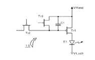
すなわち、図5はデジタル階調を実現させる3TFT方式の画素構成の例を示すものである。この図5に示す構成においては、駆動用TFT(Tr1)と、制御用TFT(Tr2)に加えて、消去用TFT(Tr3)が備えられている。この消去用TFT(Tr3)は、EL素子E1 点灯期間の途中において、当該消去用TFT(Tr3)をオン動作させることで、コンデンサC1 の電荷を放電させることができ、これによりEL素子E1 の点灯期間を制御する階調駆動を実現させることができる。この図5に示した構成においても、駆動用TFT(Tr1)および制御用TFT(Tr2)にPチャンネルを用いることで、前記した説明と同様に効率的に電源の共用化を図ることができる。
【0040】
次に図6示す構成は、いわゆるカレントミラー方式によるEL素子の駆動手段の例を示したものであり、これはカレントミラー動作により電荷保持用コンデンサC1 への書き込み処理、並びにEL素子E1 の点灯駆動動作がなされるように構成されている。すなわち、Pチャンネルの駆動用TFT(Tr1)にゲートが共通接続されて同じくPチャンネルのTFT(Tr4)が対称的に備えられており、両TFT(Tr1,Tr4)のゲートとソース間に電荷保持用のコンデンサC1 が接続されている。
【0041】
また、前記TFT(Tr4)のゲートとドレイン間には同じくPチャンネルの制御用TFT(Tr1)が接続されており、この制御用TFT(Tr1)のオン動作により、TFT(Tr1,Tr4)はカレントミラーとして機能する。すなわち、制御用TFT(Tr1)のオン動作と共にPチャンネルにより構成されたスイッチング用TFT(Tr5)もオン動作されるように構成されており、これにより、スイッチング用TFT(Tr5)を介して書き込み用電流源Is が接続されるように構成されている。
【0042】
これにより、アドレス期間においてはVHanodの電源から、TFT(TR4)、TFT(Tr5)を介して書き込み用電流源Is に流れる電流経路が形成される。またカレントミラーの作用により、電流源Is に流れる電流に対応した電流が、駆動用TFT(Tr1)を介してEL素子E1 に対して供給される。前記した動作によりコンデンサC1 には書き込み用電流源Is に流れる電流値に対応したTFT(Tr4)のゲート電圧が書き込まれる。そして、コンデンサC1 に所定の電圧値が書き込まれた後には、制御用TFT(Tr2)はオフ状態になされ、駆動用TFT(Tr1)は、コンデンサC1 に蓄積された電荷に基づいて所定の電流をEL素子E1 に供給するように作用し、これにより、EL素子E1 は発光駆動される。
【0043】
この図6に示したカレントミラー方式による駆動手段を利用した構成においても、駆動用TFT(TR1)および制御用TFT(TR2)にPチャンネルを用いることで、前記した説明と同様に効率的に電源の共用化を図ることができる。
【0044】
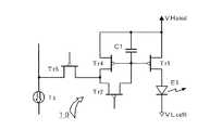
次に図7に示す構成は、電流プログラミング方式によるEL素子の駆動手段の例を示したものである。この電流プログラミング方式においては、陽極側電源(VHanod)と陰極側電源(VLcath)との間にスイッチング用TFT(Tr6)、駆動用TFT(Tr1)およびEL素子E1 の直列回路が挿入された構成とされている。また、駆動用TFT(Tr1)のソースとゲート間に電荷保持用のコンデンサC1 が接続され、駆動用TFT(Tr1)のゲートとドレインとの間には制御用TFT(Tr2)が接続されている。さらに駆動用TFT(Tr1)のソースにはスイッチング用TFT(Tr7)を介して書き込み用電流源Is が接続されている。
【0045】
図7に示した構成においては、制御用TFT(Tr2)およびスイッチング用TFT(Tr7)の各ゲートに制御信号が供給され、これらはオン状態になされる。これに伴い駆動用TFT(Tr1)もオンされ、駆動用TFT(Tr1)を介して書き込み用電流源Is からの電流が流れる。この時、書き込み用電流源Is からの電流に対応した電圧がコンデンサC1 に保持される。
【0046】
一方、EL素子の発光動作時には制御用TFT(Tr2) およびスイッチング用TFT(Tr7)は、共にオフ状態になされ、スイッチング用TFT(Tr6)がオンされる。これにより、駆動用TFT(Tr1)のソース側に、陽極側電源(VHanod)が印加され、EL素子E1 の陰極には陰極側電源(VLcath)が印加される。駆動用TFT(Tr1)のドレイン電流は、前記コンデンサC1 に保持された電荷によって決定され、EL素子の階調制御がなされる。
【0047】
この図7に示した電流プログラミング方式による駆動手段を利用した構成においても、駆動用TFT(TR1)および制御用TFT(TR2)にPチャンネルを用いることで、前記した説明と同様に効率的に電源の共用化を図ることができる。
【0048】
図8に示す構成は、電圧プログラミング方式によるEL素子の駆動手段の例を示したものである。この電圧プログラミング方式においては、駆動用TFT(Tr1)に対してスイッチング用TFT(Tr8)が直列接続され、さらに前記TFT(Tr8)にEL素子E1 が直列接続されている。また、電荷保持用のコンデンサC1 は駆動用TFT(Tr1)のゲートとソース間に接続され、また制御用のTFT(Tr2) は、駆動用TFT(Tr1)のゲートとドレイン間に接続されている。
【0049】
加えてこの電圧プログラミング方式においては、駆動用TFT(Tr1)のゲートに対して、データラインよりスイッチング用TFT(Tr9)およびコンデンサC2 を介して駆動用TFT(Tr1)のゲート側にデータ信号が供給されるように構成されている。
【0050】
前記した電圧プログラミング方式においては、TFT(Tr2) およびTFT(Tr8)がオンされ、これに伴い駆動用TFT(Tr1)のオン状態が確保される。次の瞬間にTFT(Tr8)がオフされることにより、駆動用TFT(Tr1)のドレイン電流は制御用TFT(Tr2) を介して駆動用TFT(Tr1)のゲートに回り込む。これにより、駆動用TFT(Tr1)のゲート・ソース間電圧が、TFT(Tr1)のスレッショルド電圧に等しくなるまで、ゲート・ソース間電圧が押し上げられ、この時点で駆動用TFT(Tr1)はオフする。
【0051】
そして、この時のゲート・ソース間電圧がコンデンサC1 に保持され、このコンデンサ電圧によってEL素子E1 の駆動電流が制御される。すなわち、この電圧プログラミング方式においては、駆動用TFT(Tr1)におけるスレッショルド電圧のばらつきを補償するように作用する。この図8に示した電圧プログラミング方式による駆動手段を利用した構成においても、駆動用TFT(Tr1)および制御用TFT(Tr2)にPチャンネルを用いることで、前記した説明と同様に効率的に電源の共用化を図ることができる。
【0052】
図9に示す構成は、ここではスレッショルド電圧補正方式と呼ぶことにする。この図9に示したスレッショルド電圧補正方式の例においては、駆動用TFT(Tr1)に対してEL素子E1 が直列接続され、また駆動用TFT(Tr1)のゲート・ソース間に電荷保持用のコンデンサC1 が接続されている。すなわち、この基本構成においては、図4に示した構成と同等である。
【0053】
一方、図9に示す構成においては、制御用のTFT(Tr2) のドレインと駆動用TFT(Tr1)のゲートとの間にはTFT(Tr10 )とダイオードD1 との並列接続体が挿入されている。なお、前記TFT(Tr10 )はそのゲート・ドレイン間は短絡状態に構成されており、したがってこれは制御用のTFT(Tr2) から駆動用TFT(Tr1)のゲートに向かってスレッショルド特性を与える素子として機能する。
【0054】
この構成によると、1つの画素内に形成された互いのTFTにおけるスレッショルド特性は非常に近似した特性になされるので、そのスレッショルド特性を効果的にキャンセルさせることができる。この図9に示したスレッショルド電圧補正方式による駆動手段を利用した構成においても、駆動用TFT(Tr1)および制御用TFT(Tr2)にPチャンネルを用いることで、前記した説明と同様に効率的に電源の共用化を図ることができる。
【0055】
以上の説明は、駆動用TFTおよび制御用TFTのいずれにもPチャンネル型TFTを用い、また図1に示したようにEL素子に駆動電流を供給する陽極側電源(VHanod)で、EL素子の発光輝度を調整するように構成した場合を示している。
【0056】
一方、この発明にかかる発光表示パネルの駆動装置においては、駆動用TFTおよび制御用TFTのいずれにもPチャンネル型TFTを用い、また図2に示すように、駆動用TFT(Tr1)のゲートに加える低レベル側の制御信号電圧(VLdata)で発光素子の輝度を調整するように構成した例にも適用することができる。この場合には、制御用TFT(Tr2)がオン状態となるゲート・ソース間電圧VgsをVonとすると、
VLlogi−VLdriv≧−Von
とし、
VLcont=VLdriv VLdata≧VLlogi
とすれば、制御用TFT(Tr2)はVHdataおよびVLdataに対して、共にオン状態にすることができる。これにより、同様に効率的に電源の共用化を図ることができ、本来14の電源数が必要なところを、8つの電源数で支障なく動作させることができる。
【0057】
以上説明したこの発明にかかる実施の形態においては、駆動用TFTおよび制御用TFTのいずれもが、Pチャンネルを用いた例を示している。しかしながら、駆動用TFTおよび制御用TFTのいずれもが、NチャンネルのTFTにより構成されていても、同様の作用効果を得ることができる。この場合においては、図4〜図9に示された駆動用TFT(Tr1)および制御用TFT(Tr2)は、共にNチャンネルになされる。
【0058】
そして、これらのNチャンネルにより構成された画素10の構成が図1に示された各画素10に代わって採用される。この場合には、制御用TFT(Tr2)がオン状態となるゲート・ソース間電圧VgsをVonとすると、
VLlogi−VLdriv≧Von
とし、
VLlogi=VHcont VLdriv=VHdata
とすれば、制御用TFT(Tr2)はVHdataおよびVLdataに対して、共にオン状態にすることができる。これにより、同様に効率的に電源の共用化を図ることができる。
【0059】
一方、駆動用TFTおよび制御用TFTのいずれにもNチャンネル型TFTを用い、また図2に示すように、駆動用TFT(Tr1)のゲートに加える高レベル側の制御信号電圧(VHdata)で発光素子の輝度を調整するように構成した例に適用する場合について考察すると、制御用TFT(Tr2)がオン状態となるゲート・ソース間電圧VgsをVonとすると、
VLlogi−VLdriv≧Von
とし、
VLlogi=VHcont VLdriv≧VHdata
とすれば、制御用TFT(Tr2)はVHdataおよびVLdataに対して、共にオン状態にすることができる。これにより、効率的に電源の共用化を図ることができる。
【0060】
以上説明した実施の形態においては、駆動用TFTおよび制御用TFTとして、同一チャンネルのFETを利用するようにしているが、駆動用TFTと制御用TFTに異なるチャンネルのTFTを用い、制御用TFTとしてデプレッション型のTFTを用いることにより、効率的に電源の共用化を図ることができる。図11はNチャンネルTFTにおけるデプレッション特性の例を示したものであり、周知のとおりゲート・ソース電圧がマイナス領域からドレイン電流ID が流れ始め、ゲート電圧がゼロの状態であってもオン状態の特性を呈する。
【0061】
そして、図4〜図9に示す各構成において、駆動用TFT(Tr1)はPチャンネルを用い、制御用TFT(Tr2)としてNチャンネルのデプレッション型TFTを用いた場合について考察すると、次のような電源の共用化を図ることができる。なお、以下の説明には図1に示したようにEL素子に駆動電流を供給する陽極側電源(VHanod)で、EL素子の発光輝度を調整するようにした構成において、前記条件の画素構成を採用した場合に基づくものである。
【0062】
すでに説明した共用化の例と同様に、まず、各ドライバー2,3の電源に着目した場合、
VHcolu=VHrow
であるので、これを(VHdriv)として共用化することができる。同様に、
VLcolu=VLrow
であるので、これを(VLdriv)として共用化することができる。次に駆動用TFT(Tr1)の特性が、Vgs=0VでId =0Aであるとすると、すなわち、駆動用TFTのゲート電圧を0Vとした時に、TFTがカットオフ状態になるという特性のものを使用する条件であれば、
VHdata=VHanod
としても、駆動用TFT(Tr1)をオフ状態に維持させることができる。これを(VHelem)として共用化することができる。
【0063】
一方、制御用TFT(Tr2)は、前記したとおりVgs=0Vでオン状態となるデプレッション型であるため、
VHcont=VHdata
としても、制御用TFT(Tr2)はVHdataおよびVLdataに対して、共にオン状態となる。
【0064】
そして、TFTの動作上の理由から一般的に外部ロジック電源は、前記したとおり、ドライバー電源が挟み込む次に示す電圧順位になされている。
VHdriv>VHlogi VLlogi>VLdriv
そこで、制御用TFT(Tr2)がオフ状態となるゲート・ソース間電圧VgsをVoff とすると、
VLlogi−VLdriv≧−Voff
とし、
VLcont=VLdriv VLdata=VLlogi
とすれば、制御用TFT(Tr2)はVHdataおよびVLdataに対して、共にオフ状態にすることができる。
【0065】
前記した考察に基づいて電源を共用化した結果の相関関係は、すでに説明した図10に示したものと同一になる。前記した考察に基づく電源の共有化により、本来14の電源数が必要なところを、同様に8つの電源数で、各回路を支障なく駆動させることができる。
【0066】
一方、前記したように駆動用TFT(Tr1)はPチャンネルを用い、制御用TFT(Tr2)としてNチャンネルのデプレッション型TFTを用いた場合において、図2に示すように、駆動用TFT(Tr1)のゲートに加える低レベル側の制御信号電圧(VLdata)でEL素子の輝度を調整するように構成した例に適用する場合について考察すると、次のようになる。
【0067】
すなわち、制御用TFT(Tr2)がオフ状態となるゲート・ソース間電圧VgsをVoff とすると、
VLlogi−VLdriv≧−Voff
とし、
VLcont=VLdriv VLdata≧VLlogi
とすれば、制御用TFT(Tr2)はVHdataおよびVLdataに対して、共にオフ状態にすることができる。これにより、効率的に電源の共用化を図ることができる。
【0068】
同様に、図4〜図9に示す各構成において、駆動用TFT(Tr1)にNチャンネルを用い、制御用TFT(Tr2)にPチャンネルを用い、かつ、その制御用TFT(Tr2)はVgs=0Vでオン状態であるデプレッション型のTFTを用いた場合について考察すると、次のような電源の共用化を図ることができる。なお、以下の説明には図1に示したようにEL素子に駆動電流を供給する陽極側電源(VHanod)で、EL素子の発光輝度を調整するようにした構成において、前記条件の画素構成を採用した場合に基づくものである。
【0069】
すなわち、制御用TFT(Tr2)がオフ状態となるゲート・ソース間電圧VgsをVoff とすると、
VLlogi−VLdriv≧Voff
とし、
VLlogi=VHcont VLdriv=VHdata
とすれば、制御用TFT(Tr2)はVHdataおよびVLdataに対して、共にオフ状態にすることができる。これにより、効率的に電源の共用化を図ることができる。
【0070】
さらに、駆動用TFT(Tr1)にNチャンネルを用い、制御用TFT(Tr2)にデプレッション型のPチャンネルを用い、図2に示すように、駆動用TFT(Tr1)のゲートに加える高レベル側の制御信号電圧(VHdata)でEL素子の輝度を調整するように構成した例に適用する場合について考察すると、次のようになる。
【0071】
すなわち、制御用TFT(Tr2)がオフ状態となるゲート・ソース間電圧VgsをVoff とすると、
VLlogi−VLdriv≧Voff
とし、
VLlogi=VHcont VLdriv≧VHdata
とすれば、制御用TFT(Tr2)はVHdataおよびVLdataに対して、共にオフ状態にすることができる。これにより、効率的に電源の共用化を図ることができ、電源電圧の数を低減させることができる。
【0072】
なお、以上説明した図1に示す構成においては、例えばR,G,Bに対応した3つの異なるレベルの陽極側電圧(VHanod)と、1つの陰極側電圧(VLcath)を用意して、各発光素子の発光輝度を調整するようになされている。しかしながらこの発明は、1つの陽極側電圧(VHanod)と、例えばR,G,Bに対応した3つの異なるレベルの陰極側電圧(VLcath)を用意して、各発光素子の発光輝度を調整するようにした構成にも、同様に適用することができる。この場合においても前記と同様の作用効果を得ることができる。
【図面の簡単な説明】
【図1】表示パネルを発光駆動させる場合における電源供給状態の第1例を示したブロック図である。
【図2】同じく電源供給状態の第2例を示したブロック図である。
【図3】図1に示す電源供給例において電源の共用化を図った例を示す相関図である。
【図4】この発明において好適に使用することができる第1の画素単位の回路構成例を示した結線図である。
【図5】同じく第2の画素単位の回路構成例を示した結線図である。
【図6】同じく第3の画素単位の回路構成例を示した結線図である。
【図7】同じく第4の画素単位の回路構成例を示した結線図である。
【図8】同じく第5の画素単位の回路構成例を示した結線図である。
【図9】同じく第6の画素単位の回路構成例を示した結線図である。
【図10】この発明によってなされる電源の共用化を図った例を示す相関図である。
【図11】この発明において利用されるデプレッション型TFTの特性図である。
【符号の説明】
1 表示パネル
2 データ(カラム側)ドライバー
3 走査(ロー側)ドライバー
4 コントローラ
10 画素
C1 コンデンサ
D1 ダイオード
E1 発光素子(有機EL素子)
Is 書き込み用電流源
Tr1 駆動用TFT
Tr2 制御用TFT[0001]
BACKGROUND OF THE INVENTION
The present invention relates to a drive device for a light-emitting display panel in which light-emitting elements constituting pixels are actively driven by TFTs (Thin Film Transistors), and in particular, to reduce the number of power supply voltages in a power supply circuit required to drive the light-emitting display panel. The present invention relates to a driving device for a light-emitting display panel.
[0002]
[Prior art]
The development of a display using a display panel configured by arranging light emitting elements in a matrix is being widely promoted. As a light-emitting element used for such a display panel, an organic EL (electroluminescence) element using an organic material for a light-emitting layer has attracted attention. This is also due to the fact that the use of an organic compound that can be expected to have good light-emitting characteristics for the light-emitting layer of the EL element has led to an increase in efficiency and longevity that can withstand practical use.
[0003]
As a display panel using such organic EL elements, a simple matrix type display panel in which EL elements are simply arranged in a matrix form, and an active matrix type display in which an active element made of TFT is added to each of the EL elements arranged in a matrix form. A panel has been proposed. The latter active matrix type display panel can realize lower power consumption than the former simple matrix type display panel, and has characteristics such as less crosstalk between pixels. Suitable for high definition display.
[0004]
FIG. 1 shows a circuit configuration corresponding to one pixel in a conventional active matrix display panel, a controller and a driver for individually lighting and driving each pixel, and a supply form of each power supply voltage for supplying driving power thereto. Is shown. FIG. 2 also shows another configuration example of a conventional active matrix display panel.
[0005]
In the active
[0006]
The circuit configuration corresponding to one
[0007]
Here, when considering the power supply for driving each circuit, as shown in FIGS. 1 and 2, the controller (external logic circuit) 4, the column-
[0008]
Further, in the case of configuring a full-color light-emitting display panel including R (red), G (green), and B (blue) light-emitting pixels (sub-pixels), the light-emitting efficiency of the EL elements that constitute the sub-pixels. In the example shown in FIG. 1, three different levels of anode-side voltage power supply (VHanod) and one cathode-side voltage power supply (VLcath) corresponding to R, G, and B are necessary in the example shown in FIG. become. In the example shown in FIG. 2, three different levels of data voltage power supply (VLdata) corresponding to R, G, B are required instead of the above three levels of anode side voltage power supply.
[0009]
On the other hand, it is said that a considerable amount of electron mobility is required to actively drive a current-driven light-emitting element such as the organic EL element described above. In order to drive this, a polysilicon TFT is generally used. Is used. The driving TFT (Tr1) uses a P-channel type for reasons of the structure of the EL element E1, and the control TFT (Tr2) secures a predetermined holding time with a small holding capacity. For this reason, a configuration using an N-channel type with a small leakage current at the time of OFF is considered preferable (see, for example, Non-Patent Document 1).
[0010]
[Non-Patent Document 1]
Nikkei Electronics, April 24, 2000 (No. 768)
[0011]
[Problems to be solved by the invention]
By the way, according to the example shown in FIG. 1 using the P-channel type for the driving TFT (Tr1) and the N-channel type for the control TFT (Tr2), and the example shown in FIG. It turns out that a number is necessary. Table 1 below shows more specifically examples of power supply voltages used in the configuration shown in FIG.
[0012]
[Table 1]
According to the driving device of the light emitting display panel shown in FIG. 1, the number of power supplies as shown in Table 1 is required. In particular, this kind of light emitting display panel is considered to be mounted on a portable device. In some cases, from the viewpoint of mounting space and power consumption, it is desirable to reduce the number of power supply voltages as much as possible so that they can be shared. Therefore, when trying to reduce the number of power supplies by sharing power supplies, the following sharing can be considered.
[0014]
First, when focusing on the power supply of each
VHcolu = VHrow
Therefore, this can be shared as (VHdriv). Similarly,
VLcolu = VLrow
Therefore, this can be shared as (VLdriv). Next, if the characteristics of the TFTs (Tr1, Tr2) are Vgs = 0V and Id = 0A, that is, when the gate voltages of the driving and control TFTs are set to 0V, the TFTs are cut off. If you use the one with the characteristics,
VHdata = VHanod
However, the driving TFT (Tr1) can be maintained in the OFF state. This can be shared as (VHelem). As well
VLcont = VLdata
Even so, the control TFT (Tr2) can maintain the OFF state for both VHdata and VLdata. further
VLcont = VLdata = VLdriv
However, the circuit can be operated without any trouble. Therefore, this can be shared as (VLdriv) described above.
[0015]
On the other hand, the external logic power source for driving the controller 4 shown in FIG. 1 is generally a low voltage such as 3.3 V or 2.8 V, and the TFT cannot operate at these voltages. It is impossible to share the power sources of the
VHdriv> VHlogi VLlogi> VLdriv
[0016]
Also, VHcont is used to completely turn on the control TFT (Tr2) when VHdata is written to the charge holding capacitor C1 via the control TFT (Tr2).
VHdata <VHcont
It is necessary to meet the conditions of FIG. 3 shows an example in which power sources are shared based on the above consideration. In the configuration shown in FIG. 1, it can be said that it is impossible to further reduce the number of power sources. However, as described above, it is preferable to reduce the number of power supplies from the viewpoint of mounting space and power consumption.
[0017]
The present invention has been made on the basis of the above-described viewpoints, and it is a technical problem to provide a drive device for a light-emitting display panel capable of further reducing the number of power supplies as described below. It is.
[0018]
[Means for Solving the Problems]
The present invention has been made to solve the above-mentioned problems.Of the luminous display panelThe drive deviceIt comprises at least the configuration according to the following independent claims.
[0019]
A drive device for a light-emitting display panel according to a first aspect of the present invention comprises:
An active matrix light-emitting display panel in which light-emitting pixels are arranged in a matrix form by a light-emitting element, a driving TFT that drives the light-emitting element to be turned on, and a control TFT that controls a gate voltage of the driving TFT; A driving device for a light-emitting display panel, comprising: a data driver and a scanning driver that selectively drive each light-emitting pixel of the panel; and a controller that gives a command signal based on video data to the data driver and the scanning driver. And
The data driver, the scan driver, and the controller are driven by at least two different levels of driving voltages, and the data driver has at least two different levels of control signal voltages applied to the gates of the driving TFTs. And at least two different levels of control signal voltage applied to the gate of the control TFT are supplied to the scan driver.
Low level drive voltage (VL) applied to the data drivercolu) And the scanning dryLow level drive voltage (VL) applied to the barrow) And a low level control signal voltage (VL) applied to the gate of the control TFT.cont) And VL at the same voltage leveldrivIn addition, the driving voltage on the low level side applied to the controller is VLlogiage,
In addition, at least the driving TFT and the control TFT constituting the light-emitting pixel are both configured by P-channel TFTs, and the control TFT is configured by an enhancement type TFT, and the control TFT is turned on. Gate-source voltage VgsVonWhen
[Expression 33]
VLlogi-VLdriv≧ −Von
[Expression 34]
VLlogi> VLdriv
[Expression 35]
VLcont= VLdriv
The potential relationship satisfies the conditions of
And the anode side voltage (VH) applied to the light emitting element.anod) Or cathode side voltage (VL)cath), The control signal voltage on the low level side applied to the gate of the driving TFT is VL.dataWhen
[Expression 36]
VLdata= VLlogi
It is characterized in that it has a potential relationship that satisfies the above condition.
[0020]
A drive device for a light emitting display panel according to a second aspect of the present invention comprises:
An active matrix light-emitting display panel in which light-emitting pixels are arranged in a matrix form by a light-emitting element, a driving TFT that drives the light-emitting element to be turned on, and a control TFT that controls a gate voltage of the driving TFT; A driving device for a light-emitting display panel, comprising: a data driver and a scanning driver that selectively drive each light-emitting pixel of the panel; and a controller that gives a command signal based on video data to the data driver and the scanning driver. And
The data driver, the scan driver, and the controller are driven by at least two different levels of driving voltages, and the data driver has at least two different levels of control signal voltages applied to the gates of the driving TFTs. And at least two different levels of control signal voltage applied to the gate of the control TFT are supplied to the scan driver.
Low level drive voltage (VL) applied to the data drivercolu) And a low-level drive voltage (VL) applied to the scan driver.row) And a low level control signal voltage (VL) applied to the gate of the control TFT.cont) And VL at the same voltage leveldrivIn addition, the driving voltage on the low level side applied to the controller is VLlogiage,
In addition, at least the driving TFT and the control TFT constituting the light-emitting pixel are both configured by P-channel TFTs, and the control TFT is configured by an enhancement type TFT, and the control TFT is turned on. Gate-source voltage VgsVonWhen
[Expression 37]
VLlogi-VLdriv≧ −Von
[Formula 38]
VLlogi> VLdriv
[39]
VLcont= VLdriv
The potential relationship satisfies the conditions of
The control signal voltage (VL) on the low level side applied to the gate of the driving TFTdata) To adjust the luminance of the light emitting element,
[Formula 40]
VLdata≧ VLlogi
It is characterized in that it has a potential relationship that satisfies the above condition.
[0021]
A drive device for a light emitting display panel according to a third aspect of the present invention comprises:
An active matrix light-emitting display panel in which light-emitting pixels are arranged in a matrix form by a light-emitting element, a driving TFT that drives the light-emitting element to be turned on, and a control TFT that controls a gate voltage of the driving TFT; A driving device for a light-emitting display panel, comprising: a data driver and a scanning driver that selectively drive each light-emitting pixel of the panel; and a controller that gives a command signal based on video data to the data driver and the scanning driver. And
The data driver, the scan driver, and the controller are driven by at least two different levels of driving voltages, and the data driver has at least two different levels of control signal voltages applied to the gates of the driving TFTs. And at least two different levels of control signal voltage applied to the gate of the control TFT are supplied to the scan driver.
Low level drive voltage (VL) applied to the data drivercolu) And a low-level drive voltage (VL) applied to the scan driver.row) And a low level control signal voltage (VL) applied to the gate of the control TFT.cont) And VL at the same voltage leveldrivIn addition, the driving voltage on the low level side applied to the controller is VLlogiage,
In addition, at least the driving TFT and the control TFT constituting the light-emitting pixel are both N-channel TFTs, and the control TFT is an enhancement type TFT, and the control TFT is turned on. Gate-source voltage VgsVonWhen
[Expression 41]
VLlogi-VLdriv≧ Von
[Expression 42]
VLlogi> VLdriv
The control signal voltage on the high level side applied to the gate of the control TFT is satisfied.
VHcontWhen
[Equation 43]
VLlogi= VHcont
The potential relationship satisfies the conditions of
And the anode side voltage (VH) applied to the light emitting element.anod) Or cathode side voltage (VL)cath), The high-level control signal voltage applied to the gate of the driving TFT is VH.dataWhen
(44)
VLdriv= VHdata
It is characterized in that it has a potential relationship that satisfies the above condition.
[0022]
According to a fourth aspect of the present invention, there is provided a drive device for a light emitting display panel.
An active matrix light-emitting display panel in which light-emitting pixels are arranged in a matrix form by a light-emitting element, a driving TFT that drives the light-emitting element to be turned on, and a control TFT that controls a gate voltage of the driving TFT; A driving device for a light-emitting display panel, comprising: a data driver and a scanning driver that selectively drive each light-emitting pixel of the panel; and a controller that gives a command signal based on video data to the data driver and the scanning driver. And
The data driver, the scan driver, and the controller are driven by at least two different levels of driving voltages, and the data driver has at least two different levels of control signal voltages applied to the gates of the driving TFTs. SuppliedAnd at least two different levels of control signal voltage applied to the gate of the control TFT are supplied to the scan driver,
Low level drive voltage (VL) applied to the data drivercolu) And a low-level drive voltage (VL) applied to the scan driver.row) And a low level control signal voltage (VL) applied to the gate of the control TFT.cont) And VL at the same voltage leveldrivIn addition, the driving voltage on the low level side applied to the controller is VLlogiage,
In addition, at least the driving TFT and the control TFT constituting the light-emitting pixel are both N-channel TFTs, and the control TFT is an enhancement type TFT, and the control TFT is turned on. Gate-source voltage VgsVonWhen
[Equation 45]
VLlogi-VLdriv≧ Von
[Equation 46]
VLlogi> VLdriv
The control signal voltage on the high level side applied to the gate of the control TFT is satisfied.
VHcontWhen
[Equation 47]
VLlogi= VHcont
The potential relationship satisfies the conditions of
The control signal voltage (VH on the high level side) applied to the gate of the driving TFTdata) To adjust the luminance of the light emitting element,
[Formula 48]
VLdriv≧ VHdata
It is characterized in that it has a potential relationship that satisfies the above condition.
[0023]
A drive device for a light emitting display panel according to a fifth aspect of the present invention comprises:
An active matrix light-emitting display panel in which light-emitting pixels are arranged in a matrix form by a light-emitting element, a driving TFT that drives the light-emitting element to be turned on, and a control TFT that controls a gate voltage of the driving TFT; A driving device for a light-emitting display panel, comprising: a data driver and a scanning driver that selectively drive each light-emitting pixel of the panel; and a controller that gives a command signal based on video data to the data driver and the scanning driver. And
The data driver, the scan driver, and the controller are driven by at least two different levels of driving voltages, and the data driver has at least two different levels of control signal voltages applied to the gates of the driving TFTs. And at least two different levels of control signal voltage applied to the gate of the control TFT are supplied to the scan driver.
Low level drive voltage (VL) applied to the data drivercolu) And a low-level drive voltage (VL) applied to the scan driver.row) And a low level control signal voltage (VL) applied to the gate of the control TFT.cont) And VL at the same voltage leveldrivAnd the low-level side driving potential for driving the controller is VLlogiage,
Further, at least the driving TFT constituting the light emitting pixel is constituted by a P-channel TFT and the control TFT is constituted by an N-channel TFT, and the control TFT is constituted by a depletion type TFT, and the control TFT is turned off. Gate-source voltage VgsVoffWhen
[Equation 49]
VLlogi-VLdriv≧ −Voff
[Equation 50]
VLlogi> VLdriv
[Equation 51]
VLcont= VLdriv
The potential relationship satisfies the conditions of
And the anode side voltage (VH) applied to the light emitting element.anod) Or cathode side voltage (VL)cath), The control signal voltage on the low level side applied to the gate of the driving TFT is VL.dataWhen
[Formula 52]
VLdata= VLlogi
It is characterized in that it has a potential relationship that satisfies the above condition.
[0024]
A drive device for a light emitting display panel according to a sixth aspect of the present invention comprises:
An active matrix light-emitting display panel in which light-emitting pixels are arranged in a matrix form by a light-emitting element, a driving TFT that drives the light-emitting element to be turned on, and a control TFT that controls a gate voltage of the driving TFT; A driving device for a light-emitting display panel, comprising: a data driver and a scanning driver that selectively drive each light-emitting pixel of the panel; and a controller that gives a command signal based on video data to the data driver and the scanning driver. And
The data driver, the scan driver, and the controller are driven by at least two different levels of driving voltages, and the data driver has at least two different levels of control signal voltages applied to the gates of the driving TFTs. And at least two different levels of control signal voltage applied to the gate of the control TFT are supplied to the scan driver.
Low level drive voltage (VL) applied to the data drivercolu) And a low-level drive voltage (VL) applied to the scan driver.row) And a low level control signal voltage (VL) applied to the gate of the control TFT.cont) And VL at the same voltage leveldrivAnd the low-level side drive potential for driving the controller is VLlogiage,
Further, at least the driving TFT constituting the light emitting pixel is constituted by a P-channel TFT and the control TFT is constituted by an N-channel TFT, and the control TFT is constituted by a depletion type TFT, and the control TFT is turned off. Gate-source voltage VgsVoffWhen
[Equation 53]
VLlogi-VLdriv≧ −Voff
[Formula 54]
VLlogi> VLdriv
[Expression 55]
VLcont= VLdriv
The potential relationship satisfies the conditions of
The control signal voltage (VL) on the low level side applied to the gate of the driving TFTdata) To adjust the luminance of the light emitting element,
[56]
VLdata≧ VLlogi
It is characterized in that it has a potential relationship that satisfies the above condition.
[0025]
A drive device for a light emitting display panel according to a seventh aspect of the present invention comprises:
An active matrix light-emitting display panel in which light-emitting pixels are arranged in a matrix form by a light-emitting element, a driving TFT that drives the light-emitting element to be turned on, and a control TFT that controls a gate voltage of the driving TFT; A driving device for a light-emitting display panel, comprising: a data driver and a scanning driver that selectively drive each light-emitting pixel of the panel; and a controller that gives a command signal based on video data to the data driver and the scanning driver. And
The data driver, the scan driver, and the controller have at least twoThe driving operation is performed with different levels of driving voltages, and at least two different levels of control signal voltages applied to the gate of the driving TFT are supplied to the data driver, and the scanning driver has the control TFT voltage. Configured to provide at least two different levels of control signal voltage applied to the gate;
Low level drive voltage (VL) applied to the data drivercolu) And a low-level drive voltage (VL) applied to the scan driver.row) And a low level control signal voltage (VL) applied to the gate of the control TFT.cont) And VL at the same voltage leveldrivAnd the low-level side drive potential for driving the controller is VLlogiage,
In addition, at least the driving TFT that constitutes the light emitting pixel is composed of an N-channel TFT and a control TFT is composed of a P-channel TFT, and the control TFT is composed of a depletion type TFT, and the control TFT is in an OFF state. Gate-source voltage VgsVoffWhen
[Equation 57]
VLlogi-VLdriv≧ Voff
[Formula 58]
VLlogi> VLdriv
The high-level control signal voltage applied to the gate of the control TFT is VH.contWhen
[Formula 59]
VLlogi= VHcont
The potential relationship satisfies the conditions of
And the anode side voltage (VH) applied to the light emitting element.anod) Or cathode side voltage (VL)cath), The high-level control signal voltage applied to the gate of the driving TFT is VH.dataWhen
[Expression 60]
VLdriv= VHdata
It is characterized in that it has a potential relationship that satisfies the above condition.
[0026]
A drive device for a light emitting display panel according to the invention of claim 8 is provided.
An active matrix light-emitting display panel in which light-emitting pixels are arranged in a matrix form by a light-emitting element, a driving TFT that drives the light-emitting element to be turned on, and a control TFT that controls a gate voltage of the driving TFT; A driving device for a light-emitting display panel, comprising: a data driver and a scanning driver that selectively drive each light-emitting pixel of the panel; and a controller that gives a command signal based on video data to the data driver and the scanning driver. And
The data driver, the scan driver, and the controller are driven by at least two different levels of driving voltages, and the data driver has at least two different levels of control signal voltages applied to the gates of the driving TFTs. And at least two different levels of control signal voltage applied to the gate of the control TFT are supplied to the scan driver.
Low level drive voltage (VL) applied to the data drivercolu) And a low-level drive voltage (VL) applied to the scan driver.row) And a low level control signal voltage (VL) applied to the gate of the control TFT.cont) And VL at the same voltage leveldrivAnd the low-level side drive potential for driving the controller is VLlogiage,
In addition, at least the driving TFT that constitutes the light emitting pixel is composed of an N-channel TFT and a control TFT is composed of a P-channel TFT, and the control TFT is composed of a depletion type TFT, and the control TFT is in an OFF state. Gate-source voltage VgsVoffWhen
[Equation 61]
VLlogi-VLdriv≧ Voff
[62]
VLlogi> VLdriv
The high-level control signal voltage applied to the gate of the control TFT is VH.contWhen
[Equation 63]
VLlogi= VHcont
The potential relationship satisfies the conditions of
The control signal voltage (VH on the high level side) applied to the gate of the driving TFTdata) To adjust the luminance of the light emitting element,
[Expression 64]
VLdriv≧ VHdata
It is characterized in that it has a potential relationship that satisfies the above condition.
[0027]
A drive device for a light emitting display panel according to a ninth aspect of the present invention comprises: The light-emitting element according to any one of
[0028]
DETAILED DESCRIPTION OF THE INVENTION
DESCRIPTION OF THE PREFERRED EMBODIMENTS A light emitting display panel driving apparatus according to the present invention will be described below based on the embodiments shown in the drawings. In the drive device for the light emitting display panel according to the present invention, basically, the number of power supplies is reduced by sharing power supplies, and further using the combination of operation characteristics of the drive TFT and the control TFT, The number of power supplies is reduced. In one form, the driving TFT and the control TFT are configured by the same channel.
[0029]
That is, for example, a P-channel TFT is used as the control TFT (Tr2) in the configuration shown in FIG. As a result, both the driving TFT and the control TFT are configured by the P channel. The configuration is shown in FIG. In the pixel configuration by the conductance control method shown in FIG. 4, the drain of the control TFT (Tr2) configured by the P channel is connected to the gate of the drive TFT (Tr1) also configured by the P channel. At the same time, it is connected to one terminal of a charge holding capacitor C1.
[0030]
The source of the driving TFT (Tr1) is connected to the other terminal of the capacitor and also connected to an anode side power supply (VHanod) for supplying a driving current to the EL element E1. The drain of the driving TFT (Tr1) is connected to the anode of the EL element E1, and the cathode of the EL element E1 is connected to the cathode side power supply (VHcath).
[0031]
In the configuration shown in FIG. 4, when the on-voltage is supplied from the low-side driver to the gate of the control TFT (Tr2), the control TFT (Tr2) corresponds to the control voltage from the column-side driver supplied to the source. Current flowing from the source to the drain. Therefore, the capacitor C1 is charged while the gate of the control TFT (Tr2) is on-voltage, and the voltage is supplied to the gate of the drive TFT (Tr1). Therefore, the driving TFT (Tr1) causes a current based on the gate voltage and the source voltage to flow through the EL element E1 to cause the EL element to emit light.
[0032]
When the gate of the control TFT becomes an off-voltage, the control TFT becomes a so-called cut-off, and the drain of the control TFT becomes open, but the drive TFT (Tr1) has the gate of the gate due to the charge accumulated in the capacitor C1. The voltage is maintained, the driving current is maintained until the next scanning, and the light emission of the EL element E1 is also maintained.
[0033]
Here, when the P-channel is used for the control TFT (Tr2) as shown in FIG. 4, the on / off logic of the control TFT (Tr2) in Table 1 already described is inverted. become. That is, the logic is as shown in Table 2 below, and others are as shown in Table 1.
[0034]
[Table 2]
In the configuration shown in FIG. 4, when the number of power sources is reduced by sharing power sources, the following sharing can be achieved. That is, as with the sharing example already described, when focusing on the power sources of the
VHcolu = VHrow
Therefore, this can be shared as (VHdriv). Similarly,
VLcolu = VLrow
Therefore, this can be shared as (VLdriv). Next, if the characteristics of each TFT (Tr1, Tr2) are Vgs = 0V and Id = 0A, that is, when the gate voltage of the driving and control TFTs is set to 0V, the TFTs are cut off. CharacteristicThat is, enhancement type TFTIf you use
VHdata = VHanod
However, the driving TFT (Tr1) can be maintained in the OFF state. This can be shared as (VHelem). As well
VHcont = VHdata
Even so, the control TFT (Tr2) can maintain the OFF state for both VHdata and VLdata.
[0036]
For reasons of TFT operation, the external logic power supply is generally in the following voltage order sandwiched by the driver power supply as described above.
VHdriv> VHlogi VLlogi> VLdriv
Therefore, when the gate-source voltage Vgs at which the control TFT (Tr2) is turned on is Von,
VLlogi-VLdriv≧ −Von
age,
VLcont = VLdriv VLdata = VLlogi
Then, both the control TFT (Tr2) can be turned on with respect to VHdata and VLdata.
[0037]
FIG. 10 shows the correlation of the result of sharing the power supply based on the above consideration. By sharing the power supply based on the above consideration, each circuit can be driven without any trouble with the number of eight power supplies as shown in FIG.
[0038]
The above description is based on the example of conductance control type drive control in which the drive TFT and the control TFT are both configured by the P channel. In the present invention, as shown in FIGS. Various lighting driving means can also be employed. In FIG. 5 to FIG. 9 to be described below, each part operating as the same function in the configuration already described is denoted by the same reference numeral.
[0039]
That is, FIG. 5 shows an example of a 3TFT pixel configuration for realizing digital gradation. In the configuration shown in FIG. 5, an erasing TFT (Tr3) is provided in addition to the driving TFT (Tr1) and the control TFT (Tr2). The erasing TFT (Tr3) can discharge the electric charge of the capacitor C1 by turning on the erasing TFT (Tr3) during the lighting period of the EL element E1, thereby turning on the EL element E1. Gray scale driving for controlling the period can be realized. In the configuration shown in FIG. 5 as well, by using the P channel for the driving TFT (Tr1) and the control TFT (Tr2), it is possible to efficiently share the power supply as described above.
[0040]
Next, the configuration shown in FIG. 6 shows an example of a driving means for an EL element by a so-called current mirror system. This is a writing process to the charge holding capacitor C1 by the current mirror operation and the lighting driving of the EL element E1. It is configured to operate. In other words, the gate is commonly connected to the P-channel driving TFT (Tr1) and the same P-channel TFT (Tr4) is provided symmetrically, and charge is held between the gate and source of both TFTs (Tr1, Tr4). A capacitor C1 is connected.
[0041]
Similarly, a P-channel control TFT (Tr1) is connected between the gate and drain of the TFT (Tr4). When the control TFT (Tr1) is turned on, the TFTs (Tr1, Tr4) become current. Acts as a mirror. In other words, the switching TFT (Tr5) constituted by the P channel is also turned on together with the turning on of the control TFT (Tr1), so that the writing TFT can be written via the switching TFT (Tr5). The current source Is is connected.
[0042]
As a result, a current path that flows from the power source of VHanod to the write current source Is via the TFT (TR4) and the TFT (Tr5) is formed in the address period. In addition, a current corresponding to the current flowing through the current source Is is supplied to the EL element E1 through the driving TFT (Tr1) by the action of the current mirror. Through the above operation, the gate voltage of the TFT (Tr4) corresponding to the current value flowing through the write current source Is is written into the capacitor C1. After the predetermined voltage value is written in the capacitor C1, the control TFT (Tr2) is turned off, and the driving TFT (Tr1) generates a predetermined current based on the electric charge accumulated in the capacitor C1. The EL element E1 is supplied to the EL element E1, and the EL element E1 is driven to emit light.
[0043]
Also in the configuration using the current mirror type driving means shown in FIG. 6, the P channel is used for the driving TFT (TR1) and the control TFT (TR2), so that the power can be efficiently supplied as described above. Can be shared.
[0044]
Next, the configuration shown in FIG. 7 shows an example of an EL element driving unit by a current programming method. In this current programming method, a series circuit of a switching TFT (Tr6), a driving TFT (Tr1) and an EL element E1 is inserted between an anode side power source (VHanod) and a cathode side power source (VLcath). Has been. A charge holding capacitor C1 is connected between the source and gate of the driving TFT (Tr1), and a control TFT (Tr2) is connected between the gate and drain of the driving TFT (Tr1). . Further, a write current source Is is connected to the source of the driving TFT (Tr1) via a switching TFT (Tr7).
[0045]
In the configuration shown in FIG. 7, control signals are supplied to the gates of the control TFT (Tr2) and the switching TFT (Tr7), and these are turned on. Accordingly, the driving TFT (Tr1) is also turned on, and a current from the write current source Is flows through the driving TFT (Tr1). At this time, a voltage corresponding to the current from the write current source Is is held in the capacitor C1.
[0046]
On the other hand, during the light emitting operation of the EL element, both the control TFT (Tr2) and the switching TFT (Tr7) are turned off, and the switching TFT (Tr6) is turned on. As a result, the anode side power supply (VHanod) is applied to the source side of the driving TFT (Tr1), and the cathode side power supply (VLcath) is applied to the cathode of the EL element E1. The drain current of the driving TFT (Tr1) is determined by the electric charge held in the capacitor C1, and gradation control of the EL element is performed.
[0047]
Even in the configuration using the current programming method driving means shown in FIG. 7, the P channel is used for the driving TFT (TR1) and the control TFT (TR2), so that the power source can be efficiently supplied as described above. Can be shared.
[0048]
The configuration shown in FIG. 8 shows an example of an EL element driving means by a voltage programming method. In this voltage programming method, a switching TFT (Tr8) is connected in series to a driving TFT (Tr1), and an EL element E1 is connected in series to the TFT (Tr8). The charge holding capacitor C1 is connected between the gate and source of the driving TFT (Tr1), and the control TFT (Tr2) is connected between the gate and drain of the driving TFT (Tr1). .
[0049]
In addition, in this voltage programming method, a data signal is supplied from the data line to the gate side of the driving TFT (Tr1) via the switching TFT (Tr9) and the capacitor C2 to the gate of the driving TFT (Tr1). It is configured to be.
[0050]
In the voltage programming method described above, the TFT (Tr2) and the TFT (Tr8) are turned on, and accordingly, the driving TFT (Tr1) is kept on. When the TFT (Tr8) is turned off at the next moment, the drain current of the driving TFT (Tr1) flows into the gate of the driving TFT (Tr1) through the control TFT (Tr2). As a result, the gate-source voltage is pushed up until the gate-source voltage of the driving TFT (Tr1) becomes equal to the threshold voltage of the TFT (Tr1). At this time, the driving TFT (Tr1) is turned off. .
[0051]
The gate-source voltage at this time is held in the capacitor C1, and the driving current of the EL element E1 is controlled by this capacitor voltage. In other words, this voltage programming method acts to compensate for variations in the threshold voltage in the driving TFT (Tr1). Even in the configuration using the driving means by the voltage programming method shown in FIG. 8, the power source can be efficiently supplied in the same manner as described above by using the P channel for the driving TFT (Tr1) and the control TFT (Tr2). Can be shared.
[0052]
The configuration shown in FIG. 9 is called a threshold voltage correction method here. In the example of the threshold voltage correction method shown in FIG. 9, an EL element E1 is connected in series to the driving TFT (Tr1), and a charge holding capacitor is connected between the gate and source of the driving TFT (Tr1). C1 is connected. That is, this basic configuration is equivalent to the configuration shown in FIG.
[0053]
On the other hand, in the configuration shown in FIG. 9, a parallel connection body of the TFT (Tr10) and the diode D1 is inserted between the drain of the control TFT (Tr2) and the gate of the driving TFT (Tr1). . The gate of the TFT (Tr10) is short-circuited between its gate and drain. Therefore, this is an element that gives threshold characteristics from the control TFT (Tr2) to the gate of the drive TFT (Tr1). Function.
[0054]
According to this configuration, the threshold characteristics of the mutual TFTs formed in one pixel are made to be very approximate characteristics, so that the threshold characteristics can be effectively canceled. Even in the configuration using the driving means by the threshold voltage correction method shown in FIG. 9, by using the P channel for the driving TFT (Tr1) and the control TFT (Tr2), it can be efficiently performed as described above. The power supply can be shared.
[0055]
In the above description, the P-channel TFT is used for both the driving TFT and the control TFT, and the anode side power supply (VHanod) for supplying the driving current to the EL element as shown in FIG. The case where it comprises so that light emission luminance may be adjusted is shown.
[0056]
On the other hand, in the driving device of the light emitting display panel according to the present invention, a P-channel TFT is used for both the driving TFT and the control TFT, and as shown in FIG. 2, the gate of the driving TFT (Tr1) is used. The present invention can also be applied to an example in which the luminance of the light emitting element is adjusted by the applied control signal voltage (VLdata) on the low level side. In this case, if the gate-source voltage Vgs at which the control TFT (Tr2) is turned on is Von,
VLlogi-VLdriv≧ −Von
age,
VLcont = VLdriv VLdata ≧ VLlogi
Then, both the control TFT (Tr2) can be turned on with respect to VHdata and VLdata. As a result, the power supply can be shared efficiently in the same manner, and the place where the number of power supplies of 14 is originally required can be operated without trouble with the number of power supplies of 8.
[0057]
In the embodiment according to the present invention described above, an example in which both the driving TFT and the control TFT use the P channel is shown. However, even if both the driving TFT and the control TFT are composed of N-channel TFTs, the same effect can be obtained. In this case, the driving TFT (Tr1) and the control TFT (Tr2) shown in FIGS. 4 to 9 are both N-channel.
[0058]
The configuration of the
VLlogi-VLdriv≧ Von
age,
VLlogi = VHcont VLdriv = VHdata
Then, both the control TFT (Tr2) can be turned on with respect to VHdata and VLdata. As a result, the power supply can be shared efficiently in the same manner.
[0059]
On the other hand, N-channel TFTs are used for both the driving TFT and the control TFT, and as shown in FIG. 2, light is emitted by the high-level control signal voltage (VHdata) applied to the gate of the driving TFT (Tr1). Considering the case where the present invention is applied to an example configured to adjust the luminance of the element, when the gate-source voltage Vgs at which the control TFT (Tr2) is turned on is Von,
VLlogi-VLdriv≧ Von
age,
VLlogi = VHcont VLdriv ≧ VHdata
Then, both the control TFT (Tr2) can be turned on with respect to VHdata and VLdata. Thereby, sharing of a power supply can be achieved efficiently.
[0060]
In the embodiment described above, the same channel FET is used as the driving TFT and the control TFT. However, different TFTs are used for the driving TFT and the control TFT, and the control TFT is used. By using a depletion type TFT, power can be shared efficiently. FIG. 11 shows an example of depletion characteristics in an N-channel TFT. As is well known, the drain current ID starts flowing from the negative region of the gate-source voltage, and the on-state characteristics even when the gate voltage is zero. Presents.
[0061]
4 to 9, the driving TFT (Tr1) uses the P channel, and the case where the N channel depletion type TFT is used as the control TFT (Tr2) is considered as follows. The power supply can be shared. In the following description, the pixel configuration under the above condition is used in the configuration in which the light emission luminance of the EL element is adjusted by an anode side power supply (VHanod) that supplies a drive current to the EL element as shown in FIG. This is based on the case of adoption.
[0062]
As with the example of sharing already described, when focusing on the power supply of each
VHcolu = VHrow
Therefore, this can be shared as (VHdriv). Similarly,
VLcolu = VLrow
Therefore, this can be shared as (VLdriv). Next, assuming that the characteristics of the driving TFT (Tr1) are Vgs = 0V and Id = 0A, that is, when the gate voltage of the driving TFT is 0V, the TFT is in a cutoff state. If it is a condition to use,
VHdata = VHanod
However, the driving TFT (Tr1) can be maintained in the OFF state. This can be shared as (VHelem).
[0063]
On the other hand, the control TFT (Tr2) is a depletion type that is turned on when Vgs = 0V as described above.
VHcont = VHdata
However, the control TFT (Tr2) is turned on for both VHdata and VLdata.
[0064]
For reasons of TFT operation, the external logic power supply is generally in the following voltage order sandwiched by the driver power supply as described above.
VHdriv> VHlogi VLlogi> VLdriv
Therefore, when the gate-source voltage Vgs at which the control TFT (Tr2) is turned off is Voff,
VLlogi-VLdriv≧ −Voff
age,
VLcont = VLdriv VLdata = VLlogi
Then, both the control TFT (Tr2) can be turned off with respect to VHdata and VLdata.
[0065]
The correlation as a result of sharing the power supply based on the above consideration is the same as that shown in FIG. By sharing the power supply based on the above-described consideration, each circuit can be driven without any trouble with the number of eight power supplies in the same manner where the number of power supplies of 14 is originally required.
[0066]
On the other hand, as described above, when the driving TFT (Tr1) uses the P-channel and the N-channel depletion type TFT is used as the control TFT (Tr2), as shown in FIG. 2, the driving TFT (Tr1) Considering the case where the present invention is applied to an example in which the luminance of the EL element is adjusted with the control signal voltage (VLdata) on the low level side applied to the gate, the following is obtained.
[0067]
That is, when the gate-source voltage Vgs at which the control TFT (Tr2) is turned off is Voff,
VLlogi-VLdriv≧ −Voff
age,
VLcont = VLdriv VLdata ≧ VLlogi
Then, both the control TFT (Tr2) can be turned off with respect to VHdata and VLdata. Thereby, sharing of a power supply can be achieved efficiently.
[0068]
Similarly, in each configuration shown in FIGS. 4 to 9, the N channel is used for the driving TFT (Tr1), the P channel is used for the control TFT (Tr2), and the control TFT (Tr2) has Vgs = Considering the case of using a depletion type TFT that is on at 0 V, the following power supply can be shared. In the following description, the pixel configuration under the above condition is used in the configuration in which the light emission luminance of the EL element is adjusted by an anode side power supply (VHanod) that supplies a drive current to the EL element as shown in FIG. This is based on the case of adoption.
[0069]
That is, when the gate-source voltage Vgs at which the control TFT (Tr2) is turned off is Voff,
VLlogi-VLdriv≧ Voff
age,
VLlogi = VHcont VLdriv = VHdata
Then, both the control TFT (Tr2) can be turned off with respect to VHdata and VLdata. Thereby, sharing of a power supply can be achieved efficiently.
[0070]
Further, an N channel is used for the driving TFT (Tr1) and a depletion type P channel is used for the control TFT (Tr2). As shown in FIG. 2, a high level side applied to the gate of the driving TFT (Tr1) is used. Considering the case where the present invention is applied to an example in which the luminance of the EL element is adjusted by the control signal voltage (VHdata), it is as follows.
[0071]
That is, when the gate-source voltage Vgs at which the control TFT (Tr2) is turned off is Voff,
VLlogi-VLdriv≧ Voff
age,
VLlogi = VHcont VLdriv ≧ VHdata
Then, both the control TFT (Tr2) can be turned off with respect to VHdata and VLdata. As a result, it is possible to efficiently share the power supply and reduce the number of power supply voltages.
[0072]
In the configuration shown in FIG. 1 described above, for example, three different levels of anode side voltage (VHanod) and one cathode side voltage (VLcath) corresponding to R, G, and B are prepared, and each light emission The light emission luminance of the element is adjusted. However, in the present invention, one anode side voltage (VHanod) and three different levels of cathode side voltage (VLcath) corresponding to, for example, R, G, and B are prepared, and the light emission luminance of each light emitting element is adjusted. The same can be applied to the configuration described above. Even in this case, the same effect as described above can be obtained.
[Brief description of the drawings]
FIG. 1 is a block diagram showing a first example of a power supply state when a display panel is driven to emit light.
FIG. 2 is a block diagram showing a second example of the same power supply state.
3 is a correlation diagram showing an example in which the power supply is shared in the power supply example shown in FIG. 1. FIG.
FIG. 4 is a connection diagram illustrating a circuit configuration example of a first pixel unit that can be preferably used in the present invention.
FIG. 5 is a connection diagram showing a circuit configuration example of a second pixel unit.
FIG. 6 is a connection diagram showing a circuit configuration example of a third pixel unit.
FIG. 7 is a connection diagram showing a circuit configuration example of a fourth pixel unit.
FIG. 8 is a connection diagram showing a circuit configuration example of a fifth pixel unit.
FIG. 9 is a connection diagram showing a circuit configuration example of a sixth pixel unit.
FIG. 10 is a correlation diagram showing an example in which the power supply is shared by the present invention.
FIG. 11 is a characteristic diagram of a depletion type TFT used in the present invention.
[Explanation of symbols]
1 Display panel
2 Data (column side) driver
3 Scanning (low side) driver
4 Controller
10 pixels
C1 capacitor
D1 diode
E1 Light emitting element (organic EL element)
Is current source for writing
Tr1 driving TFT
Tr2 control TFT
Claims (9)
Translated fromJapanese前記データドライバー、走査ドライバー、およびコントローラとが、少なくとも2つの異なるレベルの駆動電圧によって駆動動作がなされ、さらに前記データドライバーには前記駆動用TFTのゲートに加える少なくとも2つの異なるレベルの制御信号電圧が供給されると共に、前記走査ドライバーには前記制御用TFTのゲートに加える少なくとも2つの異なるレベルの制御信号電圧が供給されるように構成され、
前記データドライバーに加える低レベル側の駆動電圧(VLcolu)と、前記走査ドライバーに加える低レベル側の駆動電圧(VLrow )と、前記制御用TFTのゲートに加える低レベル側の制御信号電圧(VLcont)とを同一の電圧レベルで共用してVLdrivとし、また、前記コントローラに加える低レベル側の駆動電圧をVLlogiとし、
かつ、前記発光画素を構成する少なくとも前記駆動用TFTと制御用TFTとが、共にPチャンネルのTFTで構成され、また前記制御用TFTはエンハンストメント型のTFTで構成され、前記制御用TFTがオン状態となるゲート・ソース間電圧VgsをVonとした時、
かつ前記発光素子に加える陽極側電圧(VHanod)または陰極側電圧(VLcath)で発光素子の輝度を調整する構成において、前記駆動用TFTのゲートに加える低レベル側の制御信号電圧をVLdataとした時、
The data driver, the scan driver, and the controller are driven by at least two different levels of driving voltages, and the data driver has at least two different levels of control signal voltages applied to the gates of the driving TFTs. And at least two different levels of control signal voltage applied to the gate of the control TFT are supplied to the scan driver.
Low-level drive voltage (VLcolu) applied to the data driver, low-level drive voltage (VLrow) applied to the scan driver, and low-level control signal voltage (VLcont) applied to the gate of the control TFT Are shared at the same voltage level to be VLdriv, and the low-level drive voltage applied to the controller is VLlogi,
In addition, at least the driving TFT and the control TFT constituting the light-emitting pixel areboth configured byP-channel TFTs, and the control TFT is configured by anenhancement type TFT, and the control TFT is turned on. When the gate-source voltage Vgs to be in a state is Von,
In the configuration in which the luminance of the light emitting element is adjusted by the anode side voltage (VHanod) or the cathode side voltage (VLcath) applied to the light emitting element, when the control signal voltage on the low level side applied to the gate of the driving TFT is VLdata ,
前記データドライバー、走査ドライバー、およびコントローラとが、少なくとも2つの異なるレベルの駆動電圧によって駆動動作がなされ、さらに前記データドライバーには前記駆動用TFTのゲートに加える少なくとも2つの異なるレベルの制御信号電圧が供給されると共に、前記走査ドライバーには前記制御用TFTのゲートに加える少なくとも2つの異なるレベルの制御信号電圧が供給されるように構成され、
前記データドライバーに加える低レベル側の駆動電圧(VLcolu)と、前記走査ドライバーに加える低レベル側の駆動電圧(VLrow )と、前記制御用TFTのゲートに加える低レベル側の制御信号電圧(VLcont)とを同一の電圧レベルで共用してVLdrivとし、また、前記コントローラに加える低レベル側の駆動電圧をVLlogiとし、
かつ、前記発光画素を構成する少なくとも前記駆動用TFTと制御用TFTとが、共にPチャンネルのTFTで構成され、また前記制御用TFTはエンハンストメント型のTFTで構成され、前記制御用TFTがオン状態となるゲート・ソース間電圧VgsをVonとした時、
かつ前記駆動用TFTのゲートに加える低レベル側の制御信号電圧(VLdata)で発光素子の輝度を調整する構成において、
The data driver, the scan driver, and the controller are driven by at least two different levels of driving voltages, and the data driver has at least two different levels of control signal voltages applied to the gates of the driving TFTs. And at least two different levels of control signal voltage applied to the gate of the control TFT are supplied to the scan driver.
Low-level drive voltage (VLcolu) applied to the data driver, low-level drive voltage (VLrow) applied to the scan driver, and low-level control signal voltage (VLcont) applied to the gate of the control TFT Are shared at the same voltage level to be VLdriv, and the low-level drive voltage applied to the controller is VLlogi,
In addition, at least the driving TFT and the control TFT constituting the light-emitting pixel areboth configured byP-channel TFTs, thecontrol TFT isconfigured byan enhancement type TFT, and the control TFT is When the gate-source voltage Vgs to be turned on is Von,
In addition, in the configuration in which the luminance of the light emitting element is adjusted by a low level control signal voltage (VLdata) applied to the gate of the driving TFT,
前記データドライバー、走査ドライバー、およびコントローラとが、少なくとも2つの異なるレベルの駆動電圧によって駆動動作がなされ、さらに前記データドライバーには前記駆動用TFTのゲートに加える少なくとも2つの異なるレベルの制御信号電圧が供給されると共に、前記走査ドライバーには前記制御用TFTのゲートに加える少なくとも2つの異なるレベルの制御信号電圧が供給されるように構成され、
前記データドライバーに加える低レベル側の駆動電圧(VLcolu)と、前記走査ドライバーに加える低レベル側の駆動電圧(VLrow )と、前記制御用TFTのゲートに加える低レベル側の制御信号電圧(VLcont)とを同一の電圧レベルで共用してVLdrivとし、また、前記コントローラに加える低レベル側の駆動電圧をVLlogiとし、
かつ、前記発光画素を構成する少なくとも前記駆動用TFTと制御用TFTとが、共にNチャンネルのTFTで構成され、また前記制御用TFTはエンハンストメント型のTFTで構成され、前記制御用TFTがオン状態となるゲート・ソース間電圧VgsをVonとした時、
かつ前記発光素子に加える陽極側電圧(VHanod)または陰極側電圧(VLcath)で発光素子の輝度を調整する構成において、前記駆動用TFTのゲートに加える高レベル側の制御信号電圧をVHdataとした時、
The data driver, the scan driver, and the controller are driven by at least two different levels of driving voltages, and the data driver has at least two different levels of control signal voltages applied to the gates of the driving TFTs. And at least two different levels of control signal voltage applied to the gate of the control TFT are supplied to the scan driver.
Low-level drive voltage (VLcolu) applied to the data driver, low-level drive voltage (VLrow) applied to the scan driver, and low-level control signal voltage (VLcont) applied to the gate of the control TFT Are shared at the same voltage level to be VLdriv, and the low-level drive voltage applied to the controller is VLlogi,
In addition, at least the driving TFT and the control TFT constituting the light-emitting pixel areboth N-channel TFTs, and thecontrol TFT is an enhancement type TFT, and the control TFT is turned on. When the gate-source voltage Vgs to be in a state is Von,
In the configuration in which the luminance of the light emitting element is adjusted by the anode side voltage (VHanod) or the cathode side voltage (VLcath) applied to the light emitting element, when the control signal voltage on the high level side applied to the gate of the driving TFT is VHdata. ,
前記データドライバー、走査ドライバー、およびコントローラとが、少なくとも2つの異なるレベルの駆動電圧によって駆動動作がなされ、さらに前記データドライバーには前記駆動用TFTのゲートに加える少なくとも2つの異なるレベルの制御信号電圧が供給されると共に、前記走査ドライバーには前記制御用TFTのゲートに加える少なくとも2つの異なるレベルの制御信号電圧が供給されるように構成され、
前記データドライバーに加える低レベル側の駆動電圧(VLcolu)と、前記走査ドライバーに加える低レベル側の駆動電圧(VLrow )と、前記制御用TFTのゲートに加える低レベル側の制御信号電圧(VLcont)とを同一の電圧レベルで共用してVLdrivとし、また、前記コントローラに加える低レベル側の駆動電圧をVLlogiとし、
かつ、前記発光画素を構成する少なくとも前記駆動用TFTと制御用TFTとが、共にNチャンネルのTFTで構成され、また前記制御用TFTはエンハンストメント型のTFTで構成され、前記制御用TFTがオン状態となるゲート・ソース間電圧VgsをVonとした時、
かつ前記駆動用TFTのゲートに加える高レベル側の制御信号電圧(VHdata)で発光素子の輝度を調整する構成において、
The data driver, the scan driver, and the controller are driven by at least two different levels of driving voltages, and the data driver has at least two different levels of control signal voltages applied to the gates of the driving TFTs. And at least two different levels of control signal voltage applied to the gate of the control TFT are supplied to the scan driver.
Low-level drive voltage (VLcolu) applied to the data driver, low-level drive voltage (VLrow) applied to the scan driver, and low-level control signal voltage (VLcont) applied to the gate of the control TFT Are shared at the same voltage level to be VLdriv, and the low-level drive voltage applied to the controller is VLlogi,
In addition, at least the driving TFT and the control TFT constituting the light-emitting pixel areboth N-channel TFTs, and thecontrol TFT is an enhancement type TFT, and the control TFT is turned on. When the gate-source voltage Vgs to be in a state is Von,
And in the structure which adjusts the brightness | luminance of a light emitting element with the control signal voltage (VHdata) of the high level side added to the gate of the said driving TFT,
前記データドライバー、走査ドライバー、およびコントローラとが、少なくとも2つの異なるレベルの駆動電圧によって駆動動作がなされ、さらに前記データドライバーには前記駆動用TFTのゲートに加える少なくとも2つの異なるレベルの制御信号電圧が供給されると共に、前記走査ドライバーには前記制御用TFTのゲートに加える少なくとも2つの異なるレベルの制御信号電圧が供給されるように構成され、
前記データドライバーに加える低レベル側の駆動電圧(VLcolu)と、前記走査ドライバーに加える低レベル側の駆動電圧(VLrow )と、前記制御用TFTのゲートに加える低レベル側の制御信号電圧(VLcont)とを同一の電圧レベルで共用してVLdrivとし、また、前記コントローラ駆動用の低レベル側駆動電位をVLlogiとし、
かつ、前記発光画素を構成する少なくとも前記駆動用TFTがPチャンネル、制御用TFTがNチャンネルのTFTで構成され、また前記制御用TFTはデプレッション型のTFTで構成され、前記制御用TFTがオフ状態となるゲート・ソース間電圧VgsをVoff とした時、
かつ前記発光素子に加える陽極側電圧(VHanod)または陰極側電圧(VLcath)で発光素子の輝度を調整する構成において、前記駆動用TFTのゲートに加える低レベル側の制御信号電圧をVLdataとした時、
The data driver, the scan driver, and the controller are driven by at least two different levels of driving voltages, and the data driver has at least two different levels of control signal voltages applied to the gates of the driving TFTs. And at least two different levels of control signal voltage applied to the gate of the control TFT are supplied to the scan driver.
Low-level drive voltage (VLcolu) applied to the data driver, low-level drive voltage (VLrow) applied to the scan driver, and low-level control signal voltage (VLcont) applied to the gate of the control TFT Are shared at the same voltage level to be VLdriv, and the low-level drive potential for driving the controller is VLlogi,
And, at least the drivingTFT P-channel constituting the light emittingpixel, control TFTis composed of theN-channelTFT, also the control TFTis composedof ade repression type TFT, the control TFT is turned off When the gate-source voltage Vgs to be in the state is Voff,
In the configuration in which the luminance of the light emitting element is adjusted by the anode side voltage (VHanod) or the cathode side voltage (VLcath) applied to the light emitting element, when the control signal voltage on the low level side applied to the gate of the driving TFT is VLdata ,
前記データドライバー、走査ドライバー、およびコントローラとが、少なくとも2つの異なるレベルの駆動電圧によって駆動動作がなされ、さらに前記データドライバーには前記駆動用TFTのゲートに加える少なくとも2つの異なるレベルの制御信号電圧が供給されると共に、前記走査ドライバーには前記制御用TFTのゲートに加える少なくとも2つの異なるレベルの制御信号電圧が供給されるように構成され、
前記データドライバーに加える低レベル側の駆動電圧(VLcolu)と、前記走査ドライバーに加える低レベル側の駆動電圧(VLrow )と、前記制御用TFTのゲートに加える低レベル側の制御信号電圧(VLcont)とを同一の電圧レベルで共用してVLdrivとし、また、前記コントローラ駆動用の低レベル側駆動電位をVLlogiとし、
かつ、前記発光画素を構成する少なくとも前記駆動用TFTがPチャンネル、制御用TFTがNチャンネルのTFTで構成され、また前記制御用TFTはデプレッション型のTFTで構成され、前記制御用TFTがオフ状態となるゲート・ソース間電圧VgsをVoff とした時、
かつ前記駆動用TFTのゲートに加える低レベル側の制御信号電圧(VLdata)で発光素子の輝度を調整する構成において、
The data driver, the scan driver, and the controller are driven by at least two different levels of driving voltages, and the data driver has at least two different levels of control signal voltages applied to the gates of the driving TFTs. And at least two different levels of control signal voltage applied to the gate of the control TFT are supplied to the scan driver.
Low-level drive voltage (VLcolu) applied to the data driver, low-level drive voltage (VLrow) applied to the scan driver, and low-level control signal voltage (VLcont) applied to the gate of the control TFT Are shared at the same voltage level to be VLdriv, and the low-level drive potential for driving the controller is VLlogi,
And, at least the drivingTFT P-channel constituting the light emittingpixel, control TFTis composed of theN-channelTFT, also the control TFTis composedof ade repression type TFT, the control TFT is turned off When the gate-source voltage Vgs to be in the state is Voff,
In addition, in the configuration in which the luminance of the light emitting element is adjusted by a low level control signal voltage (VLdata) applied to the gate of the driving TFT,
前記データドライバー、走査ドライバー、およびコントローラとが、少なくとも2つの異なるレベルの駆動電圧によって駆動動作がなされ、さらに前記データドライバーには前記駆動用TFTのゲートに加える少なくとも2つの異なるレベルの制御信号電圧が供給されると共に、前記走査ドライバーには前記制御用TFTのゲートに加える少なくとも2つの異なるレベルの制御信号電圧が供給されるように構成され、
前記データドライバーに加える低レベル側の駆動電圧(VLcolu)と、前記走査ドライバーに加える低レベル側の駆動電圧(VLrow )と、前記制御用TFTのゲートに加える低レベル側の制御信号電圧(VLcont)とを同一の電圧レベルで共用してVLdrivとし、また、前記コントローラ駆動用の低レベル側駆動電位をVLlogiとし、
かつ、前記発光画素を構成する少なくとも前記駆動用TFTがNチャンネル、制御用TFTがPチャンネルのTFTで構成され、また前記制御用TFTはデプレッション型のTFTで構成され、前記制御用TFTがオフ状態となるゲート・ソース間電圧VgsをVoff とした時、
かつ前記発光素子に加える陽極側電圧(VHanod)または陰極側電圧(VLcath)で発光素子の輝度を調整する構成において、前記駆動用TFTのゲートに加える高レベル側の制御信号電圧をVHdataとした時、
The data driver, the scan driver, and the controller are driven by at least two different levels of driving voltages, and the data driver has at least two different levels of control signal voltages applied to the gates of the driving TFTs. And at least two different levels of control signal voltage applied to the gate of the control TFT are supplied to the scan driver.
Low-level drive voltage (VLcolu) applied to the data driver, low-level drive voltage (VLrow) applied to the scan driver, and low-level control signal voltage (VLcont) applied to the gate of the control TFT Are shared at the same voltage level to be VLdriv, and the low-level drive potential for driving the controller is VLlogi,
And, at least the drivingTFT N-channel constituting the light emittingpixel, control TFTis composed of aP-channelTFT, also the control TFTis composedof ade repression type TFT, the control TFT is turned off When the gate-source voltage Vgs to be in the state is Voff,
In the configuration in which the luminance of the light emitting element is adjusted by the anode side voltage (VHanod) or the cathode side voltage (VLcath) applied to the light emitting element, when the control signal voltage on the high level side applied to the gate of the driving TFT is VHdata. ,
前記データドライバー、走査ドライバー、およびコントローラとが、少なくとも2つの異なるレベルの駆動電圧によって駆動動作がなされ、さらに前記データドライバーには前記駆動用TFTのゲートに加える少なくとも2つの異なるレベルの制御信号電圧が供給されると共に、前記走査ドライバーには前記制御用TFTのゲートに加える少なくとも2つの異なるレベルの制御信号電圧が供給されるように構成され、
前記データドライバーに加える低レベル側の駆動電圧(VLcolu)と、前記走査ドライバーに加える低レベル側の駆動電圧(VLrow )と、前記制御用TFTのゲートに加える低レベル側の制御信号電圧(VLcont)とを同一の電圧レベルで共用してVLdrivとし、また、前記コントローラ駆動用の低レベル側駆動電位をVLlogiとし、
かつ、前記発光画素を構成する少なくとも前記駆動用TFTがNチャンネル、制御用TFTがPチャンネルのTFTで構成され、また前記制御用TFTはデプレッション型のTFTで構成され、前記制御用TFTがオフ状態となるゲート・ソース間電圧VgsをVoff とした時、
かつ前記駆動用TFTのゲートに加える高レベル側の制御信号電圧(VHdata)で発光素子の輝度を調整する構成において、
The data driver, the scan driver, and the controller are driven by at least two different levels of driving voltages, and the data driver has at least two different levels of control signal voltages applied to the gates of the driving TFTs. And at least two different levels of control signal voltage applied to the gate of the control TFT are supplied to the scan driver.
Low-level drive voltage (VLcolu) applied to the data driver, low-level drive voltage (VLrow) applied to the scan driver, and low-level control signal voltage (VLcont) applied to the gate of the control TFT Are shared at the same voltage level to be VLdriv, and the low-level drive potential for driving the controller is VLlogi,
And, at least the drivingTFT N-channel constituting the light emittingpixel, control TFTis composed of aP-channelTFT, also the control TFTis composedof ade repression type TFT, the control TFT is turned off When the gate-source voltage Vgs to be in the state is Voff,
And in the structure which adjusts the brightness | luminance of a light emitting element with the control signal voltage (VHdata) of the high level side added to the gate of the said driving TFT,
Priority Applications (1)
| Application Number | Priority Date | Filing Date | Title |
|---|---|---|---|
| JP2002294706AJP4233016B2 (en) | 2002-10-08 | 2002-10-08 | Driving device for light emitting display panel |
Applications Claiming Priority (1)
| Application Number | Priority Date | Filing Date | Title |
|---|---|---|---|
| JP2002294706AJP4233016B2 (en) | 2002-10-08 | 2002-10-08 | Driving device for light emitting display panel |
Publications (2)
| Publication Number | Publication Date |
|---|---|
| JP2004133013A JP2004133013A (en) | 2004-04-30 |
| JP4233016B2true JP4233016B2 (en) | 2009-03-04 |
Family
ID=32285169
Family Applications (1)
| Application Number | Title | Priority Date | Filing Date |
|---|---|---|---|
| JP2002294706AExpired - Fee RelatedJP4233016B2 (en) | 2002-10-08 | 2002-10-08 | Driving device for light emitting display panel |
Country Status (1)
| Country | Link |
|---|---|
| JP (1) | JP4233016B2 (en) |
Cited By (1)
| Publication number | Priority date | Publication date | Assignee | Title |
|---|---|---|---|---|
| US8438415B2 (en) | 2005-09-09 | 2013-05-07 | International Business Machines Corporation | Performing a perform timing facility function instruction for synchronizing TOD clocks |
Families Citing this family (2)
| Publication number | Priority date | Publication date | Assignee | Title |
|---|---|---|---|---|
| JP4634691B2 (en)* | 2002-10-22 | 2011-02-16 | 東芝モバイルディスプレイ株式会社 | Organic EL display device and organic EL display method |
| JP5045323B2 (en)* | 2007-09-14 | 2012-10-10 | セイコーエプソン株式会社 | Electro-optical device, control method of electro-optical device, and electronic apparatus |
- 2002
- 2002-10-08JPJP2002294706Apatent/JP4233016B2/ennot_activeExpired - Fee Related
Cited By (1)
| Publication number | Priority date | Publication date | Assignee | Title |
|---|---|---|---|---|
| US8438415B2 (en) | 2005-09-09 | 2013-05-07 | International Business Machines Corporation | Performing a perform timing facility function instruction for synchronizing TOD clocks |
Also Published As
| Publication number | Publication date |
|---|---|
| JP2004133013A (en) | 2004-04-30 |
Similar Documents
| Publication | Publication Date | Title |
|---|---|---|
| JP3949040B2 (en) | Driving device for light emitting display panel | |
| JP4062179B2 (en) | Pixel circuit, display device, and driving method of pixel circuit | |
| CN100403379C (en) | Pixel circuit, display device, and pixel circuit driving method | |
| US7215304B2 (en) | Display apparatus in which characteristics of a plurality of transistors are made to differ from one another | |
| JP5157467B2 (en) | Self-luminous display device and driving method thereof | |
| US7187350B2 (en) | Active type light emitting display device | |
| CN101615376A (en) | Display device | |
| CN101887684A (en) | Display device | |
| CN101246661A (en) | Pixel circuit and display device | |
| WO2022157822A1 (en) | Pixel circuit, display device, and method for driving same | |
| US20040263503A1 (en) | Drive devices and drive methods for light emitting display panel | |
| JP3671012B2 (en) | Display device | |
| JP5016953B2 (en) | Display element drive circuit and image display device | |
| JP2005352398A (en) | Active matrix type light emitting display panel | |
| JP4565844B2 (en) | Driving device for active matrix light emitting display panel | |
| JP4233016B2 (en) | Driving device for light emitting display panel | |
| JP2003108071A (en) | Display device | |
| JP2003228324A (en) | Display device | |
| JP2007206515A (en) | Light emitting diode driving circuit and display device using the same | |
| JP2010008941A (en) | Pixel circuit and display device | |
| WO2022162941A1 (en) | Pixel circuit and display device | |
| JP2009036933A (en) | Active matrix type light emitting display device | |
| JP4360199B2 (en) | Display device, pixel circuit, and driving method of pixel circuit | |
| JP4547873B2 (en) | Pixel circuit, display device, and driving method of pixel circuit | |
| KR101151287B1 (en) | AMOLED and driving method thereof |
Legal Events
| Date | Code | Title | Description |
|---|---|---|---|
| A621 | Written request for application examination | Free format text:JAPANESE INTERMEDIATE CODE: A621 Effective date:20050720 | |
| A977 | Report on retrieval | Free format text:JAPANESE INTERMEDIATE CODE: A971007 Effective date:20080317 | |
| A131 | Notification of reasons for refusal | Free format text:JAPANESE INTERMEDIATE CODE: A131 Effective date:20080916 | |
| A521 | Request for written amendment filed | Free format text:JAPANESE INTERMEDIATE CODE: A523 Effective date:20081113 | |
| TRDD | Decision of grant or rejection written | ||
| A01 | Written decision to grant a patent or to grant a registration (utility model) | Free format text:JAPANESE INTERMEDIATE CODE: A01 Effective date:20081205 | |
| A01 | Written decision to grant a patent or to grant a registration (utility model) | Free format text:JAPANESE INTERMEDIATE CODE: A01 | |
| A61 | First payment of annual fees (during grant procedure) | Free format text:JAPANESE INTERMEDIATE CODE: A61 Effective date:20081205 | |
| FPAY | Renewal fee payment (event date is renewal date of database) | Free format text:PAYMENT UNTIL: 20111219 Year of fee payment:3 | |
| R150 | Certificate of patent or registration of utility model | Ref document number:4233016 Country of ref document:JP Free format text:JAPANESE INTERMEDIATE CODE: R150 Free format text:JAPANESE INTERMEDIATE CODE: R150 | |
| FPAY | Renewal fee payment (event date is renewal date of database) | Free format text:PAYMENT UNTIL: 20111219 Year of fee payment:3 | |
| FPAY | Renewal fee payment (event date is renewal date of database) | Free format text:PAYMENT UNTIL: 20121219 Year of fee payment:4 | |
| FPAY | Renewal fee payment (event date is renewal date of database) | Free format text:PAYMENT UNTIL: 20121219 Year of fee payment:4 | |
| FPAY | Renewal fee payment (event date is renewal date of database) | Free format text:PAYMENT UNTIL: 20131219 Year of fee payment:5 | |
| LAPS | Cancellation because of no payment of annual fees |