JP4232788B2 - Method and system for controlling semiconductor manufacturing apparatus - Google Patents
Method and system for controlling semiconductor manufacturing apparatusDownload PDFInfo
- Publication number
- JP4232788B2 JP4232788B2JP2006101696AJP2006101696AJP4232788B2JP 4232788 B2JP4232788 B2JP 4232788B2JP 2006101696 AJP2006101696 AJP 2006101696AJP 2006101696 AJP2006101696 AJP 2006101696AJP 4232788 B2JP4232788 B2JP 4232788B2
- Authority
- JP
- Japan
- Prior art keywords
- energy
- manufacturing apparatus
- standby
- time
- control
- Prior art date
- Legal status (The legal status is an assumption and is not a legal conclusion. Google has not performed a legal analysis and makes no representation as to the accuracy of the status listed.)
- Expired - Fee Related
Links
Images


Classifications
- H—ELECTRICITY
- H01—ELECTRIC ELEMENTS
- H01L—SEMICONDUCTOR DEVICES NOT COVERED BY CLASS H10
- H01L21/00—Processes or apparatus adapted for the manufacture or treatment of semiconductor or solid state devices or of parts thereof
- H01L21/67—Apparatus specially adapted for handling semiconductor or electric solid state devices during manufacture or treatment thereof; Apparatus specially adapted for handling wafers during manufacture or treatment of semiconductor or electric solid state devices or components ; Apparatus not specifically provided for elsewhere
- H01L21/67005—Apparatus not specifically provided for elsewhere
- H01L21/67242—Apparatus for monitoring, sorting or marking
- H01L21/67276—Production flow monitoring, e.g. for increasing throughput
- G—PHYSICS
- G05—CONTROLLING; REGULATING
- G05B—CONTROL OR REGULATING SYSTEMS IN GENERAL; FUNCTIONAL ELEMENTS OF SUCH SYSTEMS; MONITORING OR TESTING ARRANGEMENTS FOR SUCH SYSTEMS OR ELEMENTS
- G05B19/00—Programme-control systems
- G05B19/02—Programme-control systems electric
- G05B19/418—Total factory control, i.e. centrally controlling a plurality of machines, e.g. direct or distributed numerical control [DNC], flexible manufacturing systems [FMS], integrated manufacturing systems [IMS] or computer integrated manufacturing [CIM]
- G05B19/41865—Total factory control, i.e. centrally controlling a plurality of machines, e.g. direct or distributed numerical control [DNC], flexible manufacturing systems [FMS], integrated manufacturing systems [IMS] or computer integrated manufacturing [CIM] characterised by job scheduling, process planning, material flow
- G—PHYSICS
- G05—CONTROLLING; REGULATING
- G05B—CONTROL OR REGULATING SYSTEMS IN GENERAL; FUNCTIONAL ELEMENTS OF SUCH SYSTEMS; MONITORING OR TESTING ARRANGEMENTS FOR SUCH SYSTEMS OR ELEMENTS
- G05B2219/00—Program-control systems
- G05B2219/30—Nc systems
- G05B2219/32—Operator till task planning
- G05B2219/32021—Energy management, balance and limit power to tools
- G—PHYSICS
- G05—CONTROLLING; REGULATING
- G05B—CONTROL OR REGULATING SYSTEMS IN GENERAL; FUNCTIONAL ELEMENTS OF SUCH SYSTEMS; MONITORING OR TESTING ARRANGEMENTS FOR SUCH SYSTEMS OR ELEMENTS
- G05B2219/00—Program-control systems
- G05B2219/30—Nc systems
- G05B2219/45—Nc applications
- G05B2219/45031—Manufacturing semiconductor wafers
- Y—GENERAL TAGGING OF NEW TECHNOLOGICAL DEVELOPMENTS; GENERAL TAGGING OF CROSS-SECTIONAL TECHNOLOGIES SPANNING OVER SEVERAL SECTIONS OF THE IPC; TECHNICAL SUBJECTS COVERED BY FORMER USPC CROSS-REFERENCE ART COLLECTIONS [XRACs] AND DIGESTS
- Y02—TECHNOLOGIES OR APPLICATIONS FOR MITIGATION OR ADAPTATION AGAINST CLIMATE CHANGE
- Y02P—CLIMATE CHANGE MITIGATION TECHNOLOGIES IN THE PRODUCTION OR PROCESSING OF GOODS
- Y02P70/00—Climate change mitigation technologies in the production process for final industrial or consumer products
- Y02P70/10—Greenhouse gas [GHG] capture, material saving, heat recovery or other energy efficient measures, e.g. motor control, characterised by manufacturing processes, e.g. for rolling metal or metal working
- Y—GENERAL TAGGING OF NEW TECHNOLOGICAL DEVELOPMENTS; GENERAL TAGGING OF CROSS-SECTIONAL TECHNOLOGIES SPANNING OVER SEVERAL SECTIONS OF THE IPC; TECHNICAL SUBJECTS COVERED BY FORMER USPC CROSS-REFERENCE ART COLLECTIONS [XRACs] AND DIGESTS
- Y02—TECHNOLOGIES OR APPLICATIONS FOR MITIGATION OR ADAPTATION AGAINST CLIMATE CHANGE
- Y02P—CLIMATE CHANGE MITIGATION TECHNOLOGIES IN THE PRODUCTION OR PROCESSING OF GOODS
- Y02P70/00—Climate change mitigation technologies in the production process for final industrial or consumer products
- Y02P70/50—Manufacturing or production processes characterised by the final manufactured product
- Y—GENERAL TAGGING OF NEW TECHNOLOGICAL DEVELOPMENTS; GENERAL TAGGING OF CROSS-SECTIONAL TECHNOLOGIES SPANNING OVER SEVERAL SECTIONS OF THE IPC; TECHNICAL SUBJECTS COVERED BY FORMER USPC CROSS-REFERENCE ART COLLECTIONS [XRACs] AND DIGESTS
- Y02—TECHNOLOGIES OR APPLICATIONS FOR MITIGATION OR ADAPTATION AGAINST CLIMATE CHANGE
- Y02P—CLIMATE CHANGE MITIGATION TECHNOLOGIES IN THE PRODUCTION OR PROCESSING OF GOODS
- Y02P80/00—Climate change mitigation technologies for sector-wide applications
- Y02P80/10—Efficient use of energy, e.g. using compressed air or pressurized fluid as energy carrier
- Y—GENERAL TAGGING OF NEW TECHNOLOGICAL DEVELOPMENTS; GENERAL TAGGING OF CROSS-SECTIONAL TECHNOLOGIES SPANNING OVER SEVERAL SECTIONS OF THE IPC; TECHNICAL SUBJECTS COVERED BY FORMER USPC CROSS-REFERENCE ART COLLECTIONS [XRACs] AND DIGESTS
- Y02—TECHNOLOGIES OR APPLICATIONS FOR MITIGATION OR ADAPTATION AGAINST CLIMATE CHANGE
- Y02P—CLIMATE CHANGE MITIGATION TECHNOLOGIES IN THE PRODUCTION OR PROCESSING OF GOODS
- Y02P90/00—Enabling technologies with a potential contribution to greenhouse gas [GHG] emissions mitigation
- Y02P90/02—Total factory control, e.g. smart factories, flexible manufacturing systems [FMS] or integrated manufacturing systems [IMS]
Landscapes
- Engineering & Computer Science (AREA)
- Automation & Control Theory (AREA)
- Physics & Mathematics (AREA)
- General Physics & Mathematics (AREA)
- Manufacturing & Machinery (AREA)
- Condensed Matter Physics & Semiconductors (AREA)
- Computer Hardware Design (AREA)
- Microelectronics & Electronic Packaging (AREA)
- Power Engineering (AREA)
- General Engineering & Computer Science (AREA)
- Quality & Reliability (AREA)
- General Factory Administration (AREA)
Description
Translated fromJapanese 本発明は、半導体製造装置の制御方法及びその制御システムに関し、特に、TATの短
縮化を妨げることなく、半導体製造装置の待機時のエネルギーロスを低減できるようにし
た技術に関する。The present invention relates to a method for controlling a semiconductor manufacturing apparatus and a control system therefor, and more particularly to a technique that can reduce energy loss during standby of a semiconductor manufacturing apparatus without hindering shortening of TAT.
半導体装置の製造ラインは、フィルタを通した清浄な空気をダウンフローさせるクリー
ンルームと、このクリーンルーム内に配置された多数の製造装置等から構成されている。
製造装置には、半導体ウエーハ中に不純物を熱拡散させるための熱処理装置や、絶縁膜を
形成するためのCVD装置、絶縁膜や導電膜を削るためのドライエッチング装置などがあ
り、その種類は多岐に渡るが、その多くは電力だけでなく、排気、冷却水、圧空、真空、
窒素(N2)、放熱等(以下、これらを電力と区別して「用力」という。)を必要とする
ものである。A semiconductor device manufacturing line is composed of a clean room for downflowing clean air that has passed through a filter, and a large number of manufacturing apparatuses arranged in the clean room.
Manufacturing equipment includes heat treatment equipment for thermally diffusing impurities in semiconductor wafers, CVD equipment for forming insulating films, and dry etching equipment for removing insulating films and conductive films. Many of them are not only power but also exhaust, cooling water, compressed air, vacuum,
Nitrogen (N2 ), heat dissipation, etc. (hereinafter these are referred to as “utility” to distinguish them from electric power).
従来、製品処理の合間で製造装置を待機させる場合には、RF電源やマグネット電源を
落としたり、ヒータの出力を多少下げたりして、その消費電力の低減を図っていたが、T
AT(Turnaround Time)の短縮化を妨げないように、製造装置のローダ
に処理すべき製品がセットされると直ぐに処理を開始できるよう準備した状態(即ち、処
理可能レベル)で、製造装置を待機させていた。Conventionally, when a manufacturing apparatus is put on standby between product processings, the RF power supply or magnet power supply is turned off or the output of the heater is lowered to reduce power consumption.
In order not to prevent the shortening of AT (Turnaround Time), when the product to be processed is set in the loader of the manufacturing apparatus, the manufacturing apparatus waits in a state ready to start processing (that is, the processable level). I was letting.
また、これ以外の低消費電力化の方法としては、例えば特許文献1に開示されたものが
ある。即ち、この特許文献1には、例えばコータデベロッパのように、半導体ウエーハに
対してそれぞれ異なる処理を行う複数のユニットを1台の中に備えた製造装置が開示され
ており、かかる製造装置にあっては、個々のユニットについてその待機時間中には電力を
供給しないようにしていた。
ところで、製造ラインを流れる製品の種類は通常一種類ではなく、多品種のものが少量
ずつ生産されることが多い。品種が異なれば製造プロセスも異なってくるので、製造ライ
ンには高頻度に使用される製造装置と、そうでない製造装置とが混在する。また、個々の
製造装置の使用頻度は、製造ラインを流れる製品の種類とその量、流れてくるタイミング
とによって日々変わることが一般的である。By the way, the type of products flowing through the production line is not usually one type, and many types of products are often produced in small quantities. Since the manufacturing process differs depending on the type, a manufacturing line that is frequently used and a manufacturing device that is not so are mixed in the manufacturing line. In addition, the frequency of use of individual manufacturing apparatuses generally varies from day to day depending on the type and amount of products flowing through the manufacturing line and the timing at which they flow.
従って、製造装置を所定のメンテナンス時まで休み無く連続して稼動させることは実際
にはほとんどなく、製品処理の合間で製造装置を待機させざるを得ないケースが多々存在
する。このような製品処理の合間の待ち時間は、数分程度と短い場合もあれば、1〜2日
程度と長い場合もある。
しかしながら、従来の技術では、製造ラインを構成する各製造装置あっては、次に製品
を処理するまでの待ち時間が短い場合も長い場合も、その待ち時間中は常に製品処理を開
始可能な処理可能レベルで待機しており、特に、待機時の待ち時間が長い場合にはそのエ
ネルギーロスが大きいという問題点があった。Therefore, it is practically rare that the manufacturing apparatus is continuously operated without a break until a predetermined maintenance time, and there are many cases in which the manufacturing apparatus is forced to wait between product processing. The waiting time between such product processes may be as short as a few minutes or as long as 1-2 days.
However, according to the conventional technology, each manufacturing apparatus constituting the manufacturing line can always start product processing during the waiting time, whether the waiting time until the next product processing is short or long. There is a problem that the energy loss is large, especially when the waiting time is long and the waiting time is long.
本発明は、このような従来の技術の有する未解決の課題に着目してなされたものであっ
て、TATの短縮化を妨げることなく、待機時のエネルギーロスを低減できるようにした
半導体製造装置の制御方法及びその制御システムの提供を目的とする。The present invention has been made paying attention to such an unsolved problem of the prior art, and a semiconductor manufacturing apparatus capable of reducing energy loss during standby without impeding shortening of TAT. An object of the present invention is to provide a control method and a control system therefor.
〔発明1〕 上記目的を達成するために、発明1の半導体製造装置の制御方法は、半導体製造装置の待機時の制御方法であって、
少なくとも前記半導体製造装置の待機時の電力及び用力所要量を製品処理が開始可能なエネルギー消費状態で待機する第1の待機状態と、前記半導体製造装置の前記待機時の電力及び用力所要量を製品処理を開始できない低エネルギー消費状態で待機する第2の待機状態とを備え、
前記半導体製造装置を含む製造ラインで製造される製品の、処理工程順に関する情報と前記処理工程毎の処理時間に関する情報と前記製造ラインでの位置に関する情報とから、前記製品が前記半導体製造装置のもとに到着するまでに要する待ち時間に関する情報を取得する工程と、
前記半導体製造装置の前記待機時の電力及び用力所要量を前記第1の待機状態から前記低エネルギー消費状態まで下げて前記第2の待機状態として所定期間維持し前記所定期間が経過した後前記第1の待機状態に戻しその後前記半導体製造装置の状態を確認する省エネ制御の所要時間に関する情報を取得する工程と、
前記所要時間が前記待ち時間よりも短く且つ前記待ち時間中に前記省エネ制御を実行した場合の消費エネルギー量が前記第1の待機状態による制御を実行した場合の消費エネルギー量よりも低減されると見積もられる場合は前記第2の待機状態による省エネ制御を実行し、前記所要時間が前記待ち時間以上である場合又は前記待ち時間中に前記省エネ制御を実行した場合の消費エネルギー量が前記第1の待機状態による制御を実行した場合の消費エネルギーよりも低減されないと見積もられる場合は前記第2の待機状態による省エネ制御を実行しないとする前記省エネ制御を実行するか否かの判断を行う工程と、を含むことを特徴とするものである。
[Invention 1] In order to achieve the above object, a control method of a semiconductor manufacturing apparatus of the
A first standby state in which at least standby power and utility requirements of the semiconductor manufacturing apparatus are on standby in an energy consumption state where product processing can be started, and the standby power and utility requirements of the semiconductor manufacturing apparatus are products. A second standby state that waits in a low energy consumption state where processing cannot be started,
The semiconductor of the products manufactured in the production line including the manufacturing apparatus, the information about the position of the information about the processing time for each information on the processing order of steps and the processing steps and the manufacturing line, priorSL product the semiconductor manufacturing device Obtaining information about the waiting time required to arrive under the
The power and utility requirements during standby of the semiconductor manufacturing apparatus arelowered from the first standby state to thelow energy consumption state andmaintained as the second standby statefor a predetermined period, and after the predetermined period has elapsed, A step of returning to the standby state of 1 and acquiring information relating to time requiredfor energy-saving controlfor confirming the state of the semiconductor manufacturing apparatus ;
When the required time is shorter than the waiting time and the amount of energy consumed when the energy saving control is executed during the waiting time is less than the amount of energy consumed when the control in the first waiting state is executed If estimated running preSL energy-saving control according to the second standby state, the required time is the energy consumption amount when executing the energy-saving control in the case where the waiting time or more or the waiting time first Determining whether or not to execute the energy saving control in which the energy saving control according to the second standby state is not executed when it is estimated that the energy consumption is not reduced when the control according to the standby state is executed. , Including.
ここで、「半導体製造装置」としては、例えばドライエッチング装置や、CVD装置、
熱処理装置等が挙げられる。これらの装置には、消費エネルギーとして例えば電力と用力
とが供給される。また、「製品」は、例えばウエーハやガラス基板等に形成される半導体
装置である。さらに、「待機時の電力及び用力所要量」とは、例えば製品処理の合間で待
機している半導体製造装置で使われる電力及び用力のことである。「用力」とは、電力以
外のエネルギーのことであり、例えば排気、冷却水、圧空、真空、窒素(N2)、放熱等
のことである。また「処理可能レベル」とは、例えば半導体製造装置のローダに処理すべ
き製品がセットされると直ぐに処理を開始できるように準備した状態のことである。Here, as the “semiconductor manufacturing apparatus”, for example, a dry etching apparatus, a CVD apparatus,
Examples include a heat treatment apparatus. For example, electric power and utility power are supplied to these devices as consumed energy. The “product” is a semiconductor device formed on, for example, a wafer or a glass substrate. Further, “standby power and utility requirements” are, for example, power and utility used in a semiconductor manufacturing apparatus waiting between product processes. “Utility” refers to energy other than electric power, such as exhaust, cooling water, compressed air, vacuum, nitrogen (N2 ), heat dissipation, and the like. The “processable level” refers to a state where preparation is made so that processing can be started as soon as a product to be processed is set in a loader of a semiconductor manufacturing apparatus, for example.
発明1の半導体製造装置の制御方法によれば、半導体製造装置の待機時の待ち時間が省
エネ制御の所要時間よりも長く、且つ待ち時間中に省エネ制御を実行することによって待
機時の消費エネルギー量が低減されると見積もられる場合のみ、省エネ制御を実行するこ
とが可能である。従って、TATの短縮化を妨げることなく、半導体製造装置の待機時の
エネルギーロスを低減することが可能である。According to the control method of the semiconductor manufacturing apparatus of the first aspect, the standby time of the semiconductor manufacturing apparatus is longer than the time required for the energy saving control, and the energy consumption amount during standby is obtained by executing the energy saving control during the waiting time. It is possible to execute the energy saving control only when it is estimated that the power consumption is reduced. Therefore, it is possible to reduce energy loss during standby of the semiconductor manufacturing apparatus without hindering shortening of TAT.
ここで、例えば熱処理装置の省エネ制御では、炉(反応室)内の温度を一旦下げ、一定時間が経過した後で炉内を加熱して元の温度に戻すことが考えられるが、一旦下げた炉内の温度を再び元の温度まで上昇させるためにはエネルギーを必要とする。そのため、省エネ制御の炉内を低温に維持するステップが短時間で終わる場合には、省エネ制御を実行することによって逆に消費エネルギー量が増えてしまうことも考えられる。
Here, for example, in the energy-saving control of the heat treatment apparatus, it is considered that the temperature in the furnace (reaction chamber) is once lowered, and after a predetermined time has passed, the furnace is heated to return to the original temperature. Energy is required to raise the temperature in the furnace back to the original temperature. Therefore, when the step of maintaining the inside of the furnace for energy saving control at a low temperature ends in a short time, it is conceivable that the amount of energy consumption increases conversely by executing the energy saving control.
発明1の半導体製造装置の制御方法によれば、半導体製造装置の待機時のエネルギーロスをより確実に低減することが可能である。 According to the method for controlling a semiconductor manufacturing apparatus of the first aspect, it is possible to more reliably reduce energy loss during standby of the semiconductor manufacturing apparatus.
〔発明2〕 発明2の半導体製造装置の制御方法は、前記第2の待機状態は、前記所要時間と消費エネルギー量とがそれぞれ異なる複数種類の制御パターンを有し、前記第2の待機状態による省ネ制御を実行するか否かを判断する工程では、前記待ち時間と前記複数種類の制御パターンそれぞれの前記所要時間とを前記複数種類の制御パターン毎にそれぞれ比較し、前記複数種類の制御パターンの中で前記所要時間が前記待ち時間よりも短い制御パターンが1つだけの場合には、当該特定パターンによる制御を前記第2の待機状態による省エネ制御として前記第2の待機状態による省エネ制御を実行するか否かの判断を行い、前記複数種類のパターンの中で前記所要時間が前記待ち時間よりも短い制御パターンが2つ以上ある場合には、当該制御パターンの中から最も待機時の消費エネルギー量が小さい制御パターンを選択し選択された当該制御パターンによる制御を前記第2の待機状態による省エネ制御として前記第2の待機状態による省エネ制御を実行するか否かの判断を行うことを特徴とするのもである。
[Invention 2] In the method for controlling a semiconductor manufacturing apparatus according to
このような構成であれば、待ち時間の長短に応じてエネルギーロスを効率良く低減するWith such a configuration, energy loss is efficiently reduced according to the waiting time.
ことが可能である。It is possible.
〔発明3〕 発明3の半導体製造装置の制御方法は、発明1から発明2の何れか一の半導
体製造装置の制御方法において、前記省エネ制御を実行している間に最新の前記待ち時間
に関する情報を取得する工程と、最新の前記待ち時間に関する情報に基づいて、実行中の
前記省エネ制御の制御パターンを見直す工程と、を含むことを特徴とするものである。
このような構成であれば、待ち時間の変動に柔軟に対応することが可能である。例えば
、省エネ制御の実行中に待ち時間が短くなった場合には、省エネ制御を途中で止めて、半
導体製造装置の電力及び用力所要量(即ち、エネルギーレベル)を処理可能レベルまで直
ちに回復させることが可能である。また、省エネ制御の実行中に待ち時間が長くなった場
合には、エネルギーレベルを低エネルギーレベルで維持する待機ステップを延長したり、
実行中の制御パターンをより低消費エネルギーなパターンに変更したりすることができる。
[Invention3 ] The control method for a semiconductor manufacturing apparatus according to
With such a configuration, it is possible to flexibly cope with fluctuations in waiting time. For example, if the waiting time becomes shorter during execution of energy-saving control, the energy-saving control is stopped halfway, and the power and utility requirements (ie energy level) of the semiconductor manufacturing equipment are immediately restored to a processable level. Is possible. Also, if the waiting time becomes longer during execution of energy saving control, the standby step for maintaining the energy level at a low energy level can be extended,
The control pattern being executed can be changed to a pattern with lower energy consumption.
〔発明4,5〕 発明4の半導体製造装置の制御方法は、前記省エネ制御を実行している間に前記待ち時間に関する最新の情報を取得する工程と、実行中の前記省エネ制御を途中で止めて前記半導体製造装置の電力及び用力所要量を前記第1の待機状態まで直ちに復帰させる場合の復帰所要時間に関する情報を取得する工程と、最新の前記待ち時間と前記復帰所要時間とを比較し、当該比較の結果に基づいて前記省エネ制御を継続するか否かを判断する工程と、を含むことを特徴とするものである。
[
発明5の半導体製造装置の制御方法は、前記半導体製造装置の前記省エネ制御を実行している間に、前記待ち時間に関する最新の情報を取得する工程と、前記復帰所要時間に関する情報を取得する工程と、前記省エネ制御を継続するか否かを判断する工程と、を当該順にしたがって繰り返し行うことを特徴とするものである。
発明4,5の半導体製造装置の制御方法によれば、省エネ制御の実行中に待ち時間が短くなった場合には当該省エネ制御を途中で止めて、半導体製造装置の電力及び用力所要量を処理可能レベルまで直ちに回復させることができる。
According to afifth aspect of the present invention, there is provided a method for controlling a semiconductor manufacturing apparatus, the step of acquiring the latest information relating to the waiting time and the information relating to the time required for return while executing the energy saving control of the semiconductor manufacturing apparatus. And the step of determining whether or not to continue the energy saving control is repeatedly performed according to the order.
According to the method for controlling a semiconductor manufacturing apparatus according to the fourth andfifth aspects of the present invention, when the waiting time becomes short during execution of the energy saving control, the energy saving control is stopped halfway to process the power and utility required amount of the semiconductor manufacturing apparatus. Immediate recovery to possible level.
〔発明6,7〕 発明6の半導体製造装置の制御方法は、前記省エネ制御を実行している間に前記待ち時間に関する最新の情報を取得する工程と、実行中の前記省エネ制御の制御パターンを他のパターンに変更した場合の新たな所要時間に関する情報を取得する工程と、最新の前記待ち時間と前記新たな所要時間とを比較すると共に、実行中の前記制御パターンを前記他のパターンに変更した場合の省エネ効果の増減を見積もり、前記比較の結果と前記見積もりの結果とに基づいて、実行中の前記制御パターンを前記他のパターンに変更するか否かを判断する工程と、を含むことを特徴とするものである。
[
発明7の半導体製造装置の制御方法は、前記半導体製造装置の前記省エネ制御を実行している間に、前記待ち時間に関する最新の情報を取得する工程と、前記新たな所要時間に関する情報を取得する工程と、実行中の前記制御パターンを前記他のパターンに変更するか否かを判断する工程と、を当該順にしたがって繰り返し行うことを特徴とするものである。
発明6,7の半導体製造装置の制御方法によれば、省エネ制御の実行中に待ち時間が長くなった場合には、当該省エネ制御の制御パターンをより省エネ効果の高いパターンに変更することができる。
According to aseventh aspect of the present invention, there is provided a method for controlling a semiconductor manufacturing apparatus, the step of acquiring the latest information regarding the waiting time and the information regarding the new required time while executing the energy saving control of the semiconductor manufacturing apparatus. The step and the step of determining whether or not to change the control pattern being executed to the other pattern are repeated in the order.
According to the control method of the semiconductor manufacturing apparatus of thesixth and seventh aspects , when the waiting time becomes long during execution of the energy saving control, the control pattern of the energy saving control can be changed to a pattern having a higher energy saving effect. .
〔発明8〕 発明8の半導体製造装置の制御方法は、前記製造ラインで製造される前記製品の処理工程順と、当該製品の前記処理工程毎の処理時間と、当該製品の前記製造ラインでの位置とから理論的に予想される時間よりも短い時間を、前記待ち時間に設定することを特徴とするものである。
このような構成であれば、省エネ制御を終える前に半導体製造装置のもとに製品が到着してしまうといった事態を絶対に起こさないようにすることができるので、省エネ制御を安心して実行することができる。
[Invention8 ] The method for controlling a semiconductor manufacturing apparatus according to
With such a configuration, it is possible to prevent a situation where the product arrives under the semiconductor manufacturing equipment before the energy-saving control is finished, so that the energy-saving control should be executed with peace of mind. Can do.
〔発明9、10〕 発明9の半導体製造装置の制御システムは、半導体製造装置の待機時の制御システムであって、
少なくとも前記半導体製造装置の待機時の電力及び用力所要量を製品処理が開始可能なエネルギー消費状態で待機する第1の待機状態と、前記半導体製造装置の前記待機時の電力及び用力所要量を製品処理を開始できない低エネルギー消費状態で待機する第2の待機状態とを備え、
前記半導体製造装置を含む製造ラインで製造される製品の、処理工程順に関する情報と前記処理工程毎の処理時間に関する情報と前記製造ラインでの位置に関する情報とから、前記製品が前記半導体製造装置のもとに到着するまでに要する待ち時間に関する情報を取得する製品情報取得手段と、
前記半導体製造装置の前記待機時の電力及び用力所要量を前記第1の待機状態から前記低エネルギー消費状態まで下げて前記第2の待機状態として所定期間維持し前記所定期間が経過した後前記第1の待機状態に戻しその後前記半導体製造装置の状態を確認する省エネ制御の所要時間に関する情報を取得する制御情報取得手段と、
前記所要時間が前記待ち時間よりも短く且つ前記待ち時間中に前記省エネ制御を実行した場合の消費エネルギー量が前記第1の待機状態による制御を実行した場合の消費エネルギー量よりも低減されると見積もられる場合は前記第2の待機状態による省エネ制御を実行し、前記所要時間が前記待ち時間以上である場合又は前記待ち時間中に前記省エネ制御を実行した場合の消費エネルギー量が前記第1の待機状態による制御を実行した場合の消費エネルギーよりも低減されないと見積もられる場合は前記第2の待機状態による省エネ制御を実行しないとする前記省エネ制御を実行するか否かを判断する判断手段と、を含むことを特徴とするものである。
[
A first standby state in which at least standby power and utility requirements of the semiconductor manufacturing apparatus are on standby in an energy consumption state where product processing can be started, and the standby power and utility requirements of the semiconductor manufacturing apparatus are products. A second standby state that waits in a low energy consumption state where processing cannot be started,
The semiconductor of the products manufactured in the production line including the manufacturing apparatus, the information about the position of the information about the processing time for each information on the processing order of steps and the processing steps and the manufacturing line, priorSL product the semiconductor manufacturing device Product information acquisition means for acquiring information about the waiting time required to arrive at
The power and utility requirements during standby of the semiconductor manufacturing apparatus arelowered from the first standby state to thelow energy consumption state andmaintained as the second standby statefor a predetermined period, and after the predetermined period has elapsed, Control information obtaining means for obtaining information relating to the time requiredfor energy-saving controlfor returning to the standby state of 1 and then confirming the state of the semiconductor manufacturing apparatus ;
When the required time is shorter than the waiting time and the amount of energy consumed when the energy saving control is executed during the waiting time is less than the amount of energy consumed when the control in the first waiting state is executed If estimated running preSL energy-saving control according to the second standby state, the required time is the energy consumption amount when executing the energy-saving control in the case where the waiting time or more or the waiting time first Determining means for determining whether or not to execute the energy saving control not to execute the energy saving control according to the second standby state when it is estimated that the energy consumption is not reduced when the control according to the standby state is executed; , Including.
発明10の半導体製造装置の制御システムは、前記製造ラインで製造される前記製品の処理工程順に関する情報と、当該製品の前記処理工程毎の処理時間に関する情報と、当該製品の前記製造ラインでの位置に関する情報とを管理する生産情報管理手段を備え、
前記製品情報取得手段は、前記処理工程順に関する情報と、前記処理時間に関する情報と、前記位置に関する情報とを前記生産情報管理手段から取得して前記待ち時間を算出することを特徴とするものである。
A control system for a semiconductor manufacturing apparatus according to atenth aspect of the present invention includes information relating to theorder of processing steps of the product manufactured in the manufacturing line, information relating to processing time for each processing step of the product, and the manufacturing line of the product. Providing production information management means to manage information about position,
The product information acquisition means acquires the information regarding the order of the processing steps, the information about the processing time, and the information about the position from the production information management means, and calculates the waiting time. is there.
ここで、「生産情報管理手段」は例えばコンピュータで構成されており、処理工程順、
処理工程毎の処理時間、各製品(例えばロット)の製造ラインでの位置など、製造ライン
を流れる複数種類の製品の生産情報を管理する機能を有するものである。
発明9,10の半導体製造装置の制御システムによれば、半導体製造装置の待機時の
待ち時間が省エネ制御の所要時間よりも長く、且つ待ち時間中に省エネ制御を実行するこ
とによって待機時の消費エネルギー量が低減されると見積もられる場合のみ、省エネ制御
を実行することが可能である。従って、TATの短縮化を妨げることなく、半導体製造装
置の待機時のエネルギーロスを低減することが可能である。
Here, the “production information management means” is constituted by a computer, for example, in order of processing steps,
It has a function of managing production information of a plurality of types of products flowing through the production line, such as the processing time for each processing step and the position of each product (for example, lot) on the production line.
According to the control system for a semiconductor manufacturing apparatus of theninth and tenth aspects of the present invention, the standby time of the semiconductor manufacturing apparatus is longer than the required time of the energy saving control, and the standby consumption is performed by executing the energy saving control during the waiting time. Only when it is estimated that the amount of energy is reduced, the energy saving control can be executed. Therefore, it is possible to reduce energy loss during standby of the semiconductor manufacturing apparatus without hindering shortening of TAT.
以下、図面を参照しながら、本発明に係る半導体製造装置の制御方法及びその制御シス
テムについて説明する。
図1は、本発明の実施の形態に係る半導体製造装置の制御システム100の構成例を示
す概念図である。Hereinafter, a control method and control system for a semiconductor manufacturing apparatus according to the present invention will be described with reference to the drawings.
FIG. 1 is a conceptual diagram showing a configuration example of a
図1に示すように、この制御システム100は、半導体装置の製造ラインに配置された
複数台の半導体製造装置(以下、単に「製造装置」という。)50a、50b、50c…
と、これらの製造装置50に例えば1台ずつ対応して配置されたパーソナルコンピュータ
(以下、「PC」という。)60a、60b、60c…と、製造ラインを流れる製品の生
産情報を管理する生産情報管理コンピュータ70と、PC60a、60b、60c…同士
及び、PC60a、60b、60c…と生産情報管理コンピュー70タとを双方向にデー
タを送受信可能に接続する信号線80と、を含んだ構成となっている。As shown in FIG. 1, the
And personal computers (hereinafter referred to as “PCs”) 60a, 60b, 60c,... Arranged in correspondence with these manufacturing apparatuses 50, for example, and production information for managing production information of products flowing through the manufacturing line. The
製造装置50a、50b、50c…は、例えばドライエッチング装置や、CVD装置、
熱処理装置等である。これらの製造装置50a、50b、50c…には、消費エネルギー
として例えば電力と用力とが供給される。また、製品は、例えばウエーハやガラス基板等
に形成される半導体装置である。さらに、生産情報管理コンピュータ70は、ROM、R
AM、ハードディスク等で構成される記憶装置と、CPUとを備えた構成となっている。
この生産情報管理コンピュータ70によって、例えば下記a〜dなどの生産情報が管理さ
れている。
a.生産機種情報
b.生産機種の工程表情報
c.生産機種・工程別の適応装置情報
d.生産機種・工程別の処理時間情報
ここで、「生産機種情報」とは、製造ラインを流れる製品の種類のことである。また、
「生産機種の工程表情報」とは、製造ラインを流れるある製品の処理工程順に関する情報
のことである。処理工程順とは、例えば、洗浄工程→ゲート酸化工程→ポリシリコン膜の
成膜工程→酸化工程→フォトリソグラフィ工程、というような順番のことである。処理工
程順は、生産機種(即ち、製品の種類)によって異なることが普通である。The
Heat treatment equipment. These
It has a configuration including a storage device including an AM, a hard disk, and the like, and a CPU.
The production
a. Production model information b. Process chart information for production models c. Applicable equipment information by production model and process d. Processing time information by production model / process Here, “production model information” refers to the type of product flowing through the production line. Also,
The “production model process chart information” is information related to the order of processing steps for a certain product flowing through the production line. The order of processing steps is, for example, the order of cleaning step → gate oxidation step → polysilicon film formation step → oxidation step → photolithography step. The order of processing steps is usually different depending on the production model (that is, the type of product).
さらに、「生産機種・工程別の適応装置情報」とは、例えばエッチング装置について、
A製品はエッチング装置α、βのどちらで処理しても構わないが、B製品はエッチング装
置αでのみ処理可能である、というような情報のことである。製造装置50a、50b、
50c…は、仮に同じ型番の装置であったとしてもその性能にはばらつきがあるので、製
品の種類毎に適応装置が限定されている場合がある。Furthermore, “applicable device information by production model / process” means, for example, an etching device,
The A product may be processed by either of the etching apparatuses α and β, but the B product can be processed only by the etching apparatus α.
Since the performance of 50c... Is different even if they are devices of the same model number, there are cases where the adaptive device is limited for each type of product.
「生産機種・工程別の処理時間情報」とは、製造ラインを流れるある製品の処理工程毎
の処理時間に関する情報のことである。例えば、洗浄工程は40分、ゲート酸化工程は3
時間、といったような処理時間に関する情報のことである。なお、同じ工程であっても製
品の種類によってその処理時間が異なる場合がある。例えば製品の種類によってゲート酸
化膜の厚さが異なる場合には、同じゲート酸化工程であってもその酸化処理時間は異なる
。一般に、ゲート酸化膜を厚く形成しようとする場合ほどその酸化処理時間は長くなる傾
向がある。“Processing time information for each production model / process” is information related to the processing time for each processing process of a certain product flowing through the production line. For example, the cleaning process is 40 minutes and the gate oxidation process is 3 minutes.
Information on processing time such as time. Even in the same process, the processing time may vary depending on the type of product. For example, when the thickness of the gate oxide film varies depending on the type of product, the oxidation treatment time differs even in the same gate oxidation process. Generally, as the gate oxide film is formed thicker, the oxidation processing time tends to be longer.
図2は、製造装置50a及びPC60aの一例を示す概念図である。ここでは、製造装
置50aの一例としてドライエッチング装置を説明する。図2に示すように、このドライ
エッチング装置50aは、平行平板型のRIE(reactive ion etchi
ng)装置であり、カセット・チャンバー10と、ロードロック・チャンバー20と、プ
ロセス・チャンバー30と、TMP(ターボ分子ポンプ)25,35及びドライポンプ1
3,23,33と、熱交換器31と、循環ポンプ32と、RF電源36と、マッチングB
OX37と、マグネット電源38と、を含んだ構成となっている。FIG. 2 is a conceptual diagram illustrating an example of the
ng) equipment,
3, 23, 33,
The configuration includes an
図2に示すように、ドライポンプ13はカセット・チャンバー10内を排気するための
ものであり、ドライポンプ23及びTMP25はロードロック・チャンバー20内を排気
するためのものである。また、ドライポンプ33及びTMP35はプロセス・チャンバー
30内を排気するためのものである。これらのポンプが排気動作することによって、各チ
ャンバー内は所定の真空度を維持することができるようになっている。As shown in FIG. 2, the
また、熱交換器31及び循環ポンプ32は、プロセス・チャンバー30内に配置された
ステージを冷却するためものである。循環ポンプ32によって、熱交換器31とステージ
との間で冷却水が循環するようになっている。さらに、RF電源36及びマッチングBO
X37は、高周波放電によってプロセス・チャンバー30内にプラズマを生成するための
ものである。マグネット電源38は、ウエーハ上でのプラズマ密度を高めるためのもので
ある。The
X37 is for generating plasma in the process chamber 30 by high frequency discharge. The
一方、PC60aは、例えば数値計算、論理演算、比較・判断などの各種処理を実行す
る機能を備えたロジックIC61と、メモリIC62等で構成されている。メモリIC6
2は例えばROMやRAM等で構成されており、シーケンス制御のプログラムが格納され
ている。また、PC60aは、ドライポンプ13,23,33及びTMP25,35と、
熱交換器31及び循環ポンプ32と、RF電源36及びマッチングBOX37と、マグネ
ット電源38とに、それぞれ信号線を介して接続している。これにより、PC60aはド
ライエッチング装置50aの製品処理(即ち、エッチング処理)に関する動作を制御でき
るようになっている。On the other hand, the
2 is composed of, for example, a ROM, a RAM, and the like, and stores a sequence control program. The
The
図3は、ドライエッチング装置50aで使われる電力(電源)及び用力の一例を示す表
図である。ここで、用力とは、電力以外のエネルギーのことであり、例えば排気、冷却水
、圧空、真空、窒素(N2)、放熱等である。図3に示すように、ドライエッチング装置
50aには、電力だけでなく、用力を消費する構成要素(機器)が多数ある。
図3中の○は、各機器が運転しており、製品処理(即ち、エッチング処理)時と同程度
の量のエネルギーを消費している状態を示している。また、図3中の△は、各機器が間欠
運転しており、○と比べてエネルギーの消費量が少ない状態を示している。さらに、図3
中で記号が無い部分(無印)では、各機器が停止している状態を示している。FIG. 3 is a table showing an example of power (power source) and utility used in the
The circles in FIG. 3 indicate that each device is in operation and consumes the same amount of energy as in product processing (that is, etching processing). In addition, Δ in FIG. 3 indicates that each device is intermittently operated and energy consumption is smaller than that of ○. In addition, FIG.
A portion without a symbol (no mark) indicates that each device is stopped.
図3に示すように、ドライエッチング装置50aの場合、スタンバイ(待機)状態は、
例えばスタンバイ−0、スタンバイ−1、スタンバイ−2に区分することができる。スタ
ンバイ−0は、製品処理を直ぐに開始できる状態である。スタンバイ−0では、RF電源
36及びマグネット電源38が停止となるものの、それ以外の機器(要素)は稼働状態を
維持し続ける。As shown in FIG. 3, in the case of the
For example, it can be classified into standby-0, standby-1, and standby-2. Standby-0 is a state in which product processing can be started immediately. In the standby-0, the
また、スタンバイ−1、2では、ドライエッチング装置50aを構成する各機器の一部
が、低消費エネルギーで待機している状態あるいは、停止状態となっており、製品処理を
直ぐには開始できない状態となっている。
即ち、スタンバイ−1では、RF電源36及びマグネット電源38と、マッチングBO
X37の冷却水とがそれぞれ止められる。また、TMPの電源及び冷却水と、ドライポン
プの電源、冷却水、N2がそれぞれ間欠運転(間欠供給)となる。つまり、スタンバイ−
1では、スタンバイ−0よりも低いスタンバイエネルギー状態で装置が待機することとな
る。また、スタンバイ−2では、スタンバイ−1に対してさらに、TMPの電源及び冷却
水がそれぞれ止められる。つまり、スタンバイ−2では、スタンバイ−1よりもさらに低
いスタンバイエネルギー状態で装置が待機することとなる。In standby-1 and 2, a part of each device constituting the
That is, in standby-1, the
The cooling water of X37 is stopped respectively. Further, the TMP power supply and cooling water, and the dry pump power supply, cooling water, and N2 are each intermittently operated (intermittent supply). In other words, standby
At 1, the device will wait in a standby energy state lower than standby-0. Further, in standby-2, the TMP power supply and the cooling water are further stopped with respect to standby-1. In other words, in standby-2, the apparatus stands by in a standby energy state lower than that in standby-1.
このように、製品処理を直ぐに開始可能なスタンバイ−0の状態と比べて、より低いエ
ネルギー状態を段階的に用意しておくことで、スタンバイ状態での消費エネルギーを段階
的に削減することができる。
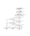
図4(A)は、省エネ制御の制御パターンの一例を示すグラフである。ここでは、省エ
ネ制御の制御パターンとして、スタンバイ−1とスタンバイ−2とを図示している。図4
(A)において、横軸は時間を示し、縦軸はエネルギー量の大きさを示している。In this way, energy consumption in the standby state can be reduced step by step by preparing a lower energy state step by step compared to the standby-0 state in which product processing can be started immediately. .
FIG. 4A is a graph illustrating an example of a control pattern of energy saving control. Here, standby-1 and standby-2 are illustrated as control patterns for energy saving control. FIG.
In (A), the horizontal axis indicates time, and the vertical axis indicates the amount of energy.
図4(A)に示すように、スタンバイ−1とスタンバイ−2の両制御パターンとも、立
下げ(CDT)、待機(STT)、立上げ(WUT)、状態確認(SCT)の4つのステ
ップで構成されている。
立下げ(CDT)は、製造装置50aを構成する各機器の少なくとも一部を、低消費エ
ネルギー状態(即ち、図3の△の状態)あるいは、停止状態(即ち、図3の無印の状態)
まで立ち下げるステップである。また、待機(STT)は、製造装置50aを構成する各
機器の少なくとも一部を低消費エネルギーあるいは、停止状態で待機させるステップであ
る。さらに、立上げ(WUT)は、低消費エネルギー状態あるいは、停止状態で待機して
いた機器を、製品処理を直ぐに開始できる状態(即ち、図3の○の状態)まで立ち上げる
ステップである。状態確認(SCT)は、立ち上げ直後の製造装置50aをスタンバイ−
0で一定時間待機させて省エネ制御の実施による装置状態(例えば、チャンバー内の真空
度等)のふらつきを自然に収束させると共に、装置状態に問題があるか無いかを確認する
ステップである。As shown in FIG. 4 (A), both standby-1 and standby-2 control patterns are performed in four steps: fall (CDT), standby (STT), rise (WUT), and status check (SCT). It is configured.
In the shutdown (CDT), at least a part of each device constituting the
It is a step to fall to. Standby (STT) is a step of waiting at least a part of each device constituting the
This is a step of waiting for a certain time at 0 to naturally converge the fluctuation of the apparatus state (for example, the degree of vacuum in the chamber) due to the execution of the energy saving control and checking whether there is a problem in the apparatus state.
図4(A)に示すように、スタンバイ時間−1(ST−1)は、スタンバイ−1を実行
する際の総所要時間であり、立下げ(CDT)、待機(STT)、立上げ(WUT)、状
態確認(SCT)の各ステップの所要時間の和である。また、スタンバイ時間−2(ST
−2)は、スタンバイ−2を実行する際の総所要時間であり、立下げ(CDT)、待機(
STT)、立上げ(WUT)、状態確認(SCT)の各ステップの所要時間の和である。
図4(A)に示すように、製造装置50aのスタンバイ時の消費エネルギー量を低くする
ほど、その立下げ(CDT)、待機(STT)、立上げ(WUT)の各ステップの所要時
間は長くなる傾向がある。本実施の形態では、スタンバイ時間−1(ST−1)<スタン
バイ時間−2(ST−2)である。As shown in FIG. 4A, standby time -1 (ST-1) is the total time required for executing standby-1 and falls (CDT), standby (STT), and rise (WUT). ), The sum of the time required for each step of the status check (SCT). Standby time -2 (ST
-2) is the total time required to execute standby-2.
This is the sum of the time required for each step of STT), start-up (WUT), and status check (SCT).
As shown in FIG. 4A, the required time for each step of the fall (CDT), standby (STT), and rise (WUT) increases as the energy consumption during standby of the
図4(B)はスタンバイ−2で製造装置50aを待機させた場合の消費エネルギー量(
STE−2)を示す概念図である。また、図4(C)はスタンバイ−0で製造装置50a
を待機させた場合の消費エネルギー量(STE−0)を示す概念図である。図4(B)及
び図4(C)において、横軸は時間を示し、縦軸はエネルギー量の大きさを示している。
図4(B)及び図4(C)に示すように、製造装置50aの待機時の消費エネルギー量
は、縦軸のエネルギー量と、横軸のスタンバイ時間とで囲まれる面積(即ち、消費エネル
ギーの積分値)で表される。スタンバイ−0と比べて、スタンバイ−2では立下げ(CD
T)及び待機(STT)ステップでの消費エネルギーは小さいものの、立上げ(WUT)
ステップでの消費エネルギーは大きい。従って、スタンバイ−2では、待機(STT)ス
テップの時間が極端に短いと、スタンバイ−0よりも消費エネルギー量が増えてしまう可
能性がある。同様に、スタンバイ−1でも、待機(STT)ステップの時間が極端に短い
と、スタンバイ−0よりも消費エネルギー量が増えてしまう可能性がある。FIG. 4B shows the amount of energy consumed when the
It is a conceptual diagram which shows STE-2). Further, FIG. 4C shows standby-0 with the
It is a conceptual diagram which shows the amount of energy consumption (STE-0) at the time of making it wait. 4B and 4C, the horizontal axis indicates time, and the vertical axis indicates the amount of energy.
As shown in FIGS. 4B and 4C, the energy consumption amount during standby of the
T) and stand-by (STT) steps consume less energy, but start up (WUT)
Energy consumption at the step is large. Therefore, in standby-2, if the time of the standby (STT) step is extremely short, there is a possibility that the amount of energy consumption will increase compared to standby-0. Similarly, even in standby-1, if the time of the standby (STT) step is extremely short, there is a possibility that the amount of energy consumption will increase compared to standby-0.
このような可能性を考慮して、本実施の形態では、スタンバイ−0を維持しているより
もスタンバイ−1、スタンバイ−2を実行した方が省エネとなるように、スタンバイ−1
、スタンバイ−2の待機(STT)時間をそれぞれ一定時間以上に設定しておく。スタン
バイ−1、スタンバイ−2において、待機(STT)の所要時間が長いほど、その消費エ
ネルギー量はスタンバイ−0と比べて小さくなる。In consideration of such a possibility, in the present embodiment, standby-1 and standby-2 are more energy efficient than standby-1 in which standby-1 and standby-2 are executed.
The standby (STT) time for standby-2 is set to a predetermined time or more. In standby-1 and standby-2, the longer the time required for standby (STT), the smaller the amount of energy consumed compared to standby-0.
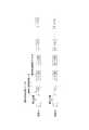
図5は、省エネ制御の制御パターンの選択方法を示すフローチャートである。まず始め
に、製造装置50aでの製品処理が終了した後で、この製造装置50aを用いて次に処理
する製品の最短製品到着時間ATを計算する(ステップS1)。このステップS1でのA
Tの計算方法については、図6を参照しながら説明する。
図6は、最短製品到着時間ATの計算方法を示すフローチャートである。FIG. 5 is a flowchart showing a method of selecting a control pattern for energy saving control. First, after the product processing in the
A method of calculating T will be described with reference to FIG.
FIG. 6 is a flowchart showing a method for calculating the shortest product arrival time AT.
まず始めに、ステップA1では、PC60aが、上述した生産情報a〜dを生産情報管
理コンピュータ70から入手する。次に、ステップA2では、製造ラインを現在流れてい
る製品または、近い将来に製造ラインに生産投入される製品の中から、製造装置50aで
処理される予定の製品を抽出する。例えば、製造ラインを流れる製品の種類として製品A
〜Zまでがあり、これらの中でドライエッチング装置50aを用いて処理する種類の製品
がAとBだけの場合を想定する。この場合には、例えば生産情報a〜cに基づいて、PC
60aが製品Aと製品Bとを抽出する。First, in step A1, the
~ Z, and the case where only products A and B are processed using the
60a extracts product A and product B.
次に、ステップA3では、製品Aを製造ラインに投入してから当該製造装置50aで処
理するまでの途中工程と、製品Bを製造ラインに投入してから当該製造装置50aで処理
するまでの途中工程とをそれぞれ抽出する。このステップA3での抽出作業は、例えば生
産情報b、cに基づいてPC60aが行う。
そして、ステップA4では、途中工程の処理標準時間−iを製品の種類(即ち、生産機
種)別にそれぞれ抽出する。例えば、図7に示すように、製品Aは、A−1工程、A−2
工程、A−3工程、A−4工程を経て、A−n工程(n:ここでは5以上の整数)で当該
製造装置50aによって製品処理される場合を想定する。この場合、ステップA4では、
A−1工程での標準処理時間は(A−1)分、A−2工程での標準処理時間は(A−2)
分というように、製品Aを処理する各工程での標準処理時間をそれぞれ抽出する。また、
当該製造装置50aは製品Bの処理も行うので、ステップA4では製品Bについても途中
工程の処理標準時間をそれぞれ抽出する。このステップA4での抽出作業は、例えば生産
情報b、c、dに基づいてPC60aが行う。Next, in step A3, an intermediate process from when the product A is introduced into the production line until it is processed by the
In step A4, the processing standard time -i of the intermediate process is extracted for each product type (ie, production model). For example, as shown in FIG.
A case is assumed in which the product is processed by the
The standard processing time in step A-1 is (A-1) minutes, and the standard processing time in step A-2 is (A-2).
As in minutes, standard processing times in each process of processing the product A are extracted. Also,
Since the
次に、ステップA5では、工程間搬送及び処理待ちの標準時間を設定する。ここでは、
図7に示すように、工程間搬送及び処理待ちの標準時間が例えば一律にtと設定されてい
るものとする。なお、実際の製造ラインでは装置の配置位置によって、工程間搬送の処理
時間がそれぞれ異なることが普通である。そのため、工程間毎に搬送及び処理待ちの標準
時間を設定しても良い。つまり、装置のレイアウトを考慮し、工程間の搬送時間を考慮す
るなどして、工程流動経路に応じた工程間時間を設定しても良い。Next, in step A5, standard time for interprocess transfer and waiting for processing is set. here,
As shown in FIG. 7, it is assumed that the standard time for interprocess transfer and waiting for processing is uniformly set to t, for example. In an actual production line, it is normal that the processing time for inter-process transfer differs depending on the arrangement position of the apparatus. Therefore, a standard time for waiting for conveyance and processing may be set for each process. That is, the inter-process time corresponding to the process flow path may be set in consideration of the layout of the apparatus and the transfer time between processes.
例えば、A−2工程とA−3工程との間の搬送及び処理待ちの標準時間をt23分とし
、A−3工程とA−4工程との間の搬送及び処理待ちの標準時間をt34分とする。A−
2工程で使用する装置とA−3工程で使用する装置は遠く離れており、A−3工程とA−
4工程で使用する装置は近接している場合には、普通はt34<t23となる。t23や
t34の値は、それぞれの工程間での搬送及び処理待ちの時間を実際に記録してその平均
値とすれば良い。For example, the standard time waiting for transfer and processing between the A-2 step and the A-3 step is t23 minutes, and the standard time waiting for transfer and processing between the A-3 step and the A-4 step is t34 minutes. And A-
The device used in
When the devices used in the four steps are close to each other, usually t34 <t23. The values of t23 and t34 may be averaged by actually recording the waiting time for conveyance and processing between the processes.
次に、ステップA6では、途中工程の総処理標準時間と、総工程間標準時間の合計を製
品の種類別にそれぞれ計算する。総処理標準時間は(1)式で、総工程間時間は(2)式
でそれぞれ算出することが可能である。この計算は例えばPC60aが行う。Next, in step A6, the total processing standard time for the intermediate process and the total standard time between all processes are calculated for each type of product. The total processing standard time can be calculated using equation (1), and the total inter-process time can be calculated using equation (2). This calculation is performed by the

(1)式、(2)式において、Nは製品A又は、製品Bの現在位置から製造装置50aに
到着するまでの途中工程の数を示す。
次に、ステップA7では、当該製造装置50aを用いて処理される予定の全ての製品A
、Bについて、その製品到着時間をそれぞれ計算する。製品到着時間は(3)式で算出す
ることが可能である。この計算は例えばPCが行う。In the formulas (1) and (2), N indicates the number of intermediate steps from the current position of the product A or the product B until reaching the
Next, in step A7, all products A to be processed using the
, B, the product arrival time is calculated. The product arrival time can be calculated by equation (3). This calculation is performed by a PC, for example.
そして、ステップA8では、ステップA7での計算結果に基づいて、製品到着時間の最
も短い製品を特定する。この特定された製品の製品到着時間が、上述の最短製品到着時間
ATである。
図5に戻って、ステップS2では、製造装置50aのスタンバイ時間であるST−1と
ST−2とをPC60aが読み込む。図4(A)に示したように、本実施の形態では、S
T−1<ST−2である。そして、ステップS3では、製造装置50aをスタンバイ−0
で待機させた場合の消費エネルギー量STE−0と、スタンバイ−1で装置を待機させた
場合の消費エネルギー量STE−1と、スタンバイ−2で装置を待機させた場合の消費エ
ネルギー量STE−2とをそれぞれPC60aが読み込む。In step A8, the product with the shortest product arrival time is specified based on the calculation result in step A7. The product arrival time of the identified product is the above-mentioned shortest product arrival time AT.
Returning to FIG. 5, in step S2, the
T-1 <ST-2. In step S3, the
Energy consumption STE-0 when the apparatus is made to stand by, energy consumption amount STE-1 when the apparatus is made to stand by at standby-1, and energy consumption amount STE-2 when the apparatus is made to stand by at standby-2 Are read by the
次に、ステップS4では、製造装置50aにおける最短製品到着時間ATと、スタンバ
イ−2の総所要時間ST−2とを比較する。ST−2よりもATの方が長い場合(即ち、
ST−2<ATの場合)には、ステップS5へ進む。また、ST−2≧ATの場合にはス
テップS7へ進む。このST−2とATとの比較及び、大小の判断はPC60aが行う。
ステップS5では、製造装置50aをスタンバイ−2で待機させた場合の消費エネルギ
ー量STE−2と、スタンバイ−1で待機させた場合の消費エネルギー量STE−1とを
比較する。STE−2よりもSTE−1が大きい場合(即ち、STE−2<STE−1の
場合)には、ステップS6へ進む。また、STE−2≧STE−1の場合にはステップS
8へ進む。このSTE−2とSTE−1との比較及び、大小の判断はPC60aが行う。Next, in step S4, the shortest product arrival time AT in the
If ST-2 <AT, the process proceeds to step S5. If ST-2 ≧ AT, the process proceeds to step S7. The comparison between ST-2 and AT and the determination of size are performed by the
In step S5, the amount of energy consumption STE-2 when the
Proceed to step 8. The comparison between STE-2 and STE-1 and the determination of the size are performed by the
ステップS6では、製造装置50aをスタンバイ−2で待機させた場合の消費エネルギ
ー量STE−2と、スタンバイ−0で待機させた場合の消費エネルギー量STE−0とを
PC60aが比較する。STE−2よりもSTE−0が大きい場合(即ち、STE−2<
STE−0の場合)にはステップS9へ進み、PC60aは製造装置50aにスタンバイ
−2の実行を指示する。また、STE−2≧STE−0の場合にはステップS11へ進み
、PC60aは製造装置50aにスタンバイ−0の実行を指示する。In step S6, the
In the case of STE-0, the process proceeds to step S9, and the
一方、ステップS7では、製造装置50aにおける最短製品到着時間ATと、スタンバ
イ−1の総所要時間ST−1とを比較する。ST−1よりもATの方が長い場合(即ち、
ST−1<ATの場合)には、ステップS8へ進む。また、ST−1≧ATの場合にはス
テップS11へ進む。このST−1とATとの比較及び、大小の判断はPC60aが行う
。On the other hand, in step S7, the shortest product arrival time AT in the
When ST-1 <AT, the process proceeds to step S8. If ST-1 ≧ AT, the process proceeds to step S11. The comparison between ST-1 and AT and the determination of size are performed by the
ステップS8では、製造装置50aをスタンバイ−1で待機させた場合の消費エネルギ
ー量STE−1と、スタンバイ−0で待機させた場合の消費エネルギー量STE−0とを
PCが比較する。STE−1よりもSTE−0が大きい場合(即ち、STE−1<STE
−0の場合)にはステップS10へ進み、PC60aは製造装置50aにスタンバイ−1
の実行を指示する。また、STE−1≧STE−0の場合にはステップS11へ進む。In step S8, the PC compares the energy consumption amount STE-1 when the
In the case of -0), the process proceeds to step S10, and the
Is instructed to execute. If STE-1 ≧ STE-0, the process proceeds to step S11.
このように、本発明の実施の形態によれば、製造装置50a、50b、50c…の待機
時の待ち時間が省エネ制御の所要時間よりも長く、且つ待ち時間中に省エネ制御を実行す
ることによって待機時の消費エネルギー量が低減されると見積もられる場合のみ、省エネ
制御を実行することが可能である。従って、TATの短縮化を妨げることなく、製造装置
50a、50b、50c…の待機時のエネルギーロスを低減することが可能である。As described above, according to the embodiment of the present invention, the standby time of the
なお、本発明では、図5のフローチャートにしたがってスタンバイ−1または、スタン
バイ−2を指示した後も、最短製品処理待ち時間ATを再取得し(即ち、最新のATを取
得し)、ATが立上げ(WUT)時間に状態確認(SCT)時間を加えた時間と等しくな
るまで、待機(STT)ステップを維持するようにしても良い。即ち、省エネ制御を実行
している間も最短製品処理待ち時間ATの再計算を繰り返し行い、図8に示すようにAT
≧WUT+SCTを満たしている間は待機(STT)時間を延長し続けても良い。In the present invention, even after the standby-1 or standby-2 is instructed according to the flowchart of FIG. 5, the shortest product processing waiting time AT is reacquired (that is, the latest AT is acquired), and the AT is established. The standby (STT) step may be maintained until it becomes equal to the time obtained by adding the state confirmation (SCT) time to the raising (WUT) time. In other words, the re-calculation of the shortest product processing waiting time AT is repeatedly performed while the energy saving control is executed, and the AT is processed as shown in FIG.
As long as ≧ WUT + SCT is satisfied, the standby (STT) time may be extended.
図9は、省エネ制御の延長方法を示すフローチャートである。まず始めに、ステップB
1で、次に処理する製品の最短製品到着時間ATを計算する。このステップB1でのAT
の計算方法は、図5のステップS1での計算方法と同じである。次に、ステップB2では
、実行中のスタンバイ状態で、装置立上げ時間WUT(i)と、確認時間SCT(i)と
をPC60aが読み込む。ここで、iは制御パターンの種類を示す整数である。例えば、
スタンバイ−2を実行している場合は、製造装置50aの立上げに要する時間WUT(2
)と、装置の確認時間SCT(2)とをPC60aが読み込む。FIG. 9 is a flowchart showing a method for extending energy saving control. First, step B
1, the shortest product arrival time AT of the product to be processed next is calculated. AT at this step B1
The calculation method is the same as the calculation method in step S1 of FIG. Next, in step B2, the
When standby-2 is being executed, the time WUT (2 required for starting up the
) And the confirmation time SCT (2) of the apparatus are read by the
そして、ステップB3では、立上げ時間WUT(i)に確認時間SCT(i)を加えた
時間と、最短製品到着時間ATとをPC60aが比較する。AT≦WUT(i)+SCT
(i)の場合にはステップB4へ進み、立上げ(WUT)ステップを開始する。また、A
T>WUT(i)+SCT(i)の場合は、ステップB1に戻り、待機(STT)ステッ
プを維持しつつ、最短到着時間ATの再計算を行う。つまり、AT≦WUT(i)+SC
T(i)を満足するまで、待機(STT)ステップを維持しつつ、ステップB1〜B3を
繰り返し行う。In step B3, the
In the case of (i), the process proceeds to step B4, and a start-up (WUT) step is started. A
If T> WUT (i) + SCT (i), the process returns to step B1, and the shortest arrival time AT is recalculated while maintaining the standby (STT) step. That is, AT ≦ WUT (i) + SC
Steps B1 to B3 are repeated while maintaining the standby (STT) step until T (i) is satisfied.
このように本発明によれば、待ち時間の変動に柔軟に対応することが可能である。即ち
、省エネ制御の実行中に待ち時間が短くなった場合には、省エネ制御を途中で止めて、製
造装置50aの電力及び用力所要量(即ち、エネルギーレベル)を処理可能レベルまで直
ちに回復させることが可能である。また、省エネ制御の実行中に待ち時間が長くなった場
合には、エネルギーレベルを低エネルギーレベルで維持する待機(STT)ステップを延
長することができる。As described above, according to the present invention, it is possible to flexibly cope with fluctuations in waiting time. That is, when the waiting time becomes shorter during execution of the energy saving control, the energy saving control is stopped halfway, and the power and utility required amount (that is, the energy level) of the
また、本発明では、省エネ制御の実行中に待ち時間が長くなった場合には、その制御パ
ターンをより省エネ効果の高いパターンに変更しても良い。例えば、図10に示すように
、スタンバイ−1を実行中に最短製品到着時間ATをPC60aが再取得する(即ち、最
新のATを取得する)と共に、このAT再取得時点でスタンバイ−1からスタンバイ−2
に変更した場合の省エネ制御の所要時間ST−2´をPC60aが計算する。また、AT
再取得時点でスタンバイ−1をスタンバイ−2に変更した場合に予想される省エネ効果(
即ち、消費エネルギー量の増減)をPC60aが算出する。Moreover, in this invention, when waiting time becomes long during execution of energy saving control, you may change the control pattern into a pattern with a higher energy saving effect. For example, as shown in FIG. 10, the
The
Energy saving effect expected when standby-1 is changed to standby-2 at the time of reacquisition (
That is, the
そして、AT≧ST−2´で、且つスタンバイ−1からスタンバイ−2に変更した方が
消費エネルギー量が低減するとPC60aが判断した場合には、図10に示すようにスタ
ンバイレベルをスタンバイ−1からスタンバイ−2に変更する。一方、AT<ST−2の
場合や、スタンバイレベルの変更によって省エネ効果が悪化するような場合にはスタンバ
イレベルの変更は行わない。When the
このように本発明によれば、省エネ制御の実行中に待ち時間が長くなった場合には、当
該省エネ制御の制御パターンをより省エネ効果の高いパターンに変更することができるの
で、待ち時間の変動に柔軟に対応しつつ省エネ効果を高めていくことが可能である。最短
製品到着時間ATは製造ラインのトラブルや、生産計画の見直し等によって変動すること
が多いので、このようなスタンバイレベルの見直しは省エネ制御の実行中にPC60aが
繰り返し行うことが好ましい。As described above, according to the present invention, when the waiting time becomes longer during execution of the energy saving control, the control pattern of the energy saving control can be changed to a pattern having a higher energy saving effect. It is possible to increase the energy-saving effect while responding flexibly. Since the shortest product arrival time AT often fluctuates due to a trouble in the production line, a review of the production plan, etc., it is preferable that such a review of the standby level is repeatedly performed by the
また、本発明では、必ずしも最短製品到着時間ATを正確に確定しなくても良い。装置
毎に消費エネルギーを削減するに必要な時間以上に製品処理待ちが続く事がわかった場合
(例えば、あと6時間は最低製品が流れてこない、といったような場合)には、この予測
時間に基づいて例えば図5や、図9のフローチャートを実行しても良い。
さらに、本発明では最短製品到着時間ATを、製造ラインを流れる製品の処理工程順と
、当該製品の処理工程毎の処理時間と、当該製品の製造ラインでの位置とから理論的に予
想される時間よりも短い時間(即ち、製品が製造装置のもとに絶対に到着することのない
時間)に設定してもよい。例えば、(3)式において、総工程間時間を0と見なして、製
品処理待ち時間=総処理標準時間としても良い。In the present invention, the shortest product arrival time AT is not necessarily determined accurately. If it is found that product processing waits longer than the time required to reduce energy consumption for each device (for example, the minimum product does not flow for another 6 hours), this estimated time For example, the flowcharts of FIGS. 5 and 9 may be executed.
Further, in the present invention, the shortest product arrival time AT is theoretically predicted from the order of the processing steps of the product flowing through the production line, the processing time for each processing step of the product, and the position of the product on the manufacturing line. It may be set to a time shorter than the time (that is, a time when the product never arrives at the manufacturing apparatus). For example, in the expression (3), the total inter-process time may be regarded as 0, and the product processing waiting time may be set to the total processing standard time.
このような構成であれば、省エネ制御を終える前に製造装置50aのもとに製品が到着
してしまうといった事態を絶対に起こさないようにすることができるので、省エネ制御を
安心して実行することができる。
この実施の形態では、PC60a(又はPC60b、PC60c)が本発明の「製品情
報取得手段」と「制御情報取得手段」と「判断手段」とに対応している。また、生産情報
管理コンピュータ70が本発明の「生産情報管理手段」に対応している。With such a configuration, it is possible to prevent a situation in which a product arrives under the
In this embodiment, the
10 カセット・チャンバー、13,23,33 ドライポンプ 20 ロードロック
・チャンバー、25,35 TMP 30 プロセス・チャンバー、31 熱交換器、3
2 循環ポンプ、36 RF電源、37 マッチングBOX、50a 製造装置(一例と
して、ドライエッチング装置)、50b、50c 製造装置、60a、60b、60c
PC、61 ロジックIC、62 メモリIC、70 生産情報管理コンピュータ、10
0 制御システム10 Cassette chamber, 13, 23, 33 Dry pump 20 Load lock chamber, 25, 35 TMP 30 Process chamber, 31 Heat exchanger, 3
2 Circulating pump, 36 RF power supply, 37 Matching BOX, 50a Manufacturing apparatus (for example, dry etching apparatus), 50b, 50c Manufacturing apparatus, 60a, 60b, 60c
PC, 61 logic IC, 62 memory IC, 70 production information management computer, 10
0 control system
Claims (10)
Translated fromJapanese少なくとも前記半導体製造装置の待機時の電力及び用力所要量を製品処理が開始可能なエネルギー消費状態で待機する第1の待機状態と、前記半導体製造装置の前記待機時の電力及び用力所要量を製品処理を開始できない低エネルギー消費状態で待機する第2の待機状態とを備え、
前記半導体製造装置を含む製造ラインで製造される製品の、処理工程順に関する情報と前記処理工程毎の処理時間に関する情報と前記製造ラインでの位置に関する情報とから、前記製品が前記半導体製造装置のもとに到着するまでに要する待ち時間に関する情報を取得する工程と、
前記半導体製造装置の前記待機時の電力及び用力所要量を前記第1の待機状態から前記低エネルギー消費状態まで下げて前記第2の待機状態として所定期間維持し前記所定期間が経過した後前記第1の待機状態に戻しその後前記半導体製造装置の状態を確認する省エネ制御の所要時間に関する情報を取得する工程と、
前記所要時間が前記待ち時間よりも短く且つ前記待ち時間中に前記省エネ制御を実行した場合の消費エネルギー量が前記第1の待機状態による制御を実行した場合の消費エネルギー量よりも低減されると見積もられる場合は前記第2の待機状態による省エネ制御を実行し、前記所要時間が前記待ち時間以上である場合又は前記待ち時間中に前記省エネ制御を実行した場合の消費エネルギー量が前記第1の待機状態による制御を実行した場合の消費エネルギーよりも低減されないと見積もられる場合は前記第2の待機状態による省エネ制御を実行しないとする前記省エネ制御を実行するか否かの判断を行う工程と、を含むことを特徴とする半導体製造装置の制御方法。A method of controlling a semiconductor manufacturing apparatus during standby,
A first standby state in which at least standby power and utility requirements of the semiconductor manufacturing apparatus are on standby in an energy consumption state where product processing can be started, and the standby power and utility requirements of the semiconductor manufacturing apparatus are products. A second standby state that waits in a low energy consumption state where processing cannot be started,
The semiconductor of the products manufactured in the production line including the manufacturing apparatus, the information about the position of the information about the processing time for each information on the processing order of steps and the processing steps and the manufacturing line, priorSL product the semiconductor manufacturing device Obtaining information about the waiting time required to arrive under the
The power and utility requirements during standby of the semiconductor manufacturing apparatus arelowered from the first standby state to thelow energy consumption state andmaintained as the second standby statefor a predetermined period, and after the predetermined period has elapsed, A step of returning to the standby state of 1 and acquiring information relating to time requiredfor energy-saving controlfor confirming the state of the semiconductor manufacturing apparatus ;
When the required time is shorter than the waiting time and the amount of energy consumed when the energy saving control is executed during the waiting time is less than the amount of energy consumed when the control in the first waiting state is executed If estimated running preSL energy-saving control according to the second standby state, the required time is the energy consumption amount when executing the energy-saving control in the case where the waiting time or more or the waiting time first Determining whether or not to execute the energy saving control in which the energy saving control according to the second standby state is not executed when it is estimated that the energy consumption is not reduced when the control according to the standby state is executed. A method for controlling a semiconductor manufacturing apparatus, comprising:
前記第2の待機状態による省エネ制御を実行するか否かを判断する工程では、
前記待ち時間と前期複数種類の制御パターンそれぞれの前記所要時間とを前記複数種類の制御パターン毎にそれぞれ比較し、
前記複数種類の制御パターンの中で前記所要時間が前記待ち時間よりも短い制御パターンが1つだけの場合には、当該特定パターンによる制御を前記第2の待機状態による省エネ制御として前記第2の待機状態による省エネ制御を実行するか否かの判断を行い、前記複数種類のパターンの中で前記所要時間が前記待ち時間よりも短い制御パターンが2つ以上ある場合には、当該制御パターンの中から最も待機時の消費エネルギー量が小さい制御パターンを選択し選択された当該制御パターンによる制御を前記第2の待機状態による省エネ制御として前記第2の待機状態による省エネ制御を実行するか否かの判断を行うことを特徴とする請求項1に記載の半導体製造装置の制御方法。The second standby state in the previous period has a plurality of types of control patterns in which the required time and energy consumption are different from each other,
In the step of determining whether or not to execute the energy saving control by the second standby state,
The waiting time and the required time for each of the plurality of types of control patterns in the previous period are compared for each of the plurality of types of control patterns,
In the case where there is only one control pattern in which the required time is shorter than the waiting time among the plurality of types of control patterns, the control based on the specific pattern is the energy saving control based on the second standby state. It is determined whether or not to execute energy saving control in a standby state, and when there are two or more control patterns in which the required time is shorter than the waiting time among the plurality of types of patterns, Whether or not to execute the energy-saving control in the second standby state as the energy-saving control in the second standby state by selecting the control pattern with the smallest amount of energy consumption during standby from the selected control pattern The method for controlling a semiconductor manufacturing apparatus according to claim 1, wherein the determination is performed.
最新の前記待ち時間に関する情報に基づいて、実行中の前記省エネ制御の制御パターンを見直す工程と、
を含むことを特徴とする請求項1から請求項2の何れか一項に記載の半導体製造装置の制御方法。Obtaining information about the latest waiting time while executing the energy saving control;
Reviewing the control pattern of the energy-saving control being executed based on the latest information on the waiting time;
The method for controlling a semiconductor manufacturing apparatus according to any one of claims 1 to2 , further comprising:
実行中の前記省エネ制御を途中で止めて前記半導体製造装置の電力及び用力所要量を前
記第1の待機状態まで直ちに復帰させる場合の復帰所要時間に関する情報を取得する工程
と、
最新の前記待ち時間と前記復帰所要時間とを比較し、当該比較の結果に基づいて前記省
エネ制御を継続するか否かを判断する工程と、を含むことを特徴とする請求項1から請求
項2の何れか一項に記載の半導体製造装置の制御方法。Obtaining the latest information on the waiting time while executing the energy-saving control;
A step of obtaining information relating to a time required for return when stopping the energy-saving control being executed halfway and immediately returning the power and power requirement of the semiconductor manufacturing apparatus to the first standby state;
The method includes a step of comparing the latest waiting time with the time required for return and determining whether or not to continue the energy saving control based on a result of the comparison.3. A method for controlling a semiconductor manufacturing apparatus according to any one of2 above.
前記待ち時間に関する最新の情報を取得する工程と、前記復帰所要時間に関する情報を
取得する工程と、前記省エネ制御を継続するか否かを判断する工程と、を当該順にしたが
って繰り返し行うことを特徴とする請求項4に記載の半導体製造装置の制御方法。While executing the energy saving control of the semiconductor manufacturing apparatus,
The step of obtaining the latest information on the waiting time, the step of obtaining information on the return required time, and the step of determining whether or not to continue the energy saving control are repeatedly performed according to the order. The method for controlling a semiconductor manufacturing apparatus according to claim4 .
実行中の前記省エネ制御の制御パターンを他のパターンに変更した場合の新たな所要時
間に関する情報を取得する工程と、
最新の前記待ち時間と前記新たな所要時間とを比較すると共に、実行中の前記制御パタ
ーンを前記他のパターンに変更した場合の省エネ効果の増減を見積もり、前記比較の結果と
前記見積もりの結果とに基づいて、実行中の前記制御パターンを前記他のパターンに変更
するか否かを判断する工程と、を含むことを特徴とする請求項1から請求項2の何れか一
項に記載の半導体製造装置の制御方法。Obtaining the latest information on the waiting time while executing the energy-saving control;
Obtaining information on a new required time when the control pattern of the energy saving control being executed is changed to another pattern;
The latest waiting time and the new required time are compared, and the increase / decrease in energy saving effect when the control pattern being executed is changed to the other pattern is estimated, and the result of the comparison and the result of the estimation based on, according to the control pattern being executed in any one of claims2 to claim 1, characterized in that it comprises a step of determining whether to change to the other pattern semiconductor Control method of manufacturing equipment.
前記待ち時間に関する最新の情報を取得する工程と、前記新たな所要時間に関する情報
を取得する工程と、実行中の前記制御パターンを前記他のパターンに変更するか否かを判
断する工程と、を当該順にしたがって繰り返し行うことを特徴とする請求項6に記載の半
導体製造装置の制御方法。While executing the energy saving control of the semiconductor manufacturing apparatus,
Obtaining the latest information on the waiting time, obtaining information on the new required time, and determining whether to change the control pattern being executed to the other pattern. 7. The method of controlling a semiconductor manufacturing apparatus according to claim6 , wherein the control is repeatedly performed in this order.
間と、当該製品の前記製造ラインでの位置とから理論的に予想される時間よりも短い時間を、前記待ち時間に設定することを特徴とする請求項1から請求項7の何れか一項に記載の半導体製造装置の制御方法。A time shorter than the theoretically expected time from theorder of the processing steps of the product manufactured in the manufacturing line, the processing time of each processing step of the product, and the position of the product in the manufacturing line. the control method of a semiconductor manufacturing apparatus according to claims 1 to any one of claims7, characterized in that to set the waiting time.
少なくとも前記半導体製造装置の待機時の電力及び用力所要量を製品処理が開始可能なエネルギー消費状態で待機する第1の待機状態と、前記半導体製造装置の前記待機時の電力及び用力所要量を製品処理を開始できない低エネルギー消費状態で待機する第2の待機状態とを備え、
前記半導体製造装置を含む製造ラインで製造される製品の、処理工程順に関する情報と前記処理工程毎の処理時間に関する情報と前記製造ラインでの位置に関する情報とから、前記製品が前記半導体製造装置のもとに到着するまでに要する待ち時間に関する情報を取得する製品情報取得手段と、
前記半導体製造装置の前記待機時の電力及び用力所要量を前記第1の待機状態から前記低エネルギー消費状態まで下げて前記第2の待機状態として所定期間維持し前記所定期間が経過した後前記第1の待機状態に戻しその後前記半導体製造装置の状態を確認する省エネ制御の所要時間に関する情報を取得する制御情報取得手段と、
前記所要時間が前記待ち時間よりも短く且つ前記待ち時間中に前記省エネ制御を実行した場合の消費エネルギー量が前記第1の待機状態による制御を実行した場合の消費エネルギー量よりも低減されると見積もられる場合は前記第2の待機状態による省エネ制御を実行し、前記所要時間が前記待ち時間以上である場合又は前記待ち時間中に前記省エネ制御を実行した場合の消費エネルギー量が前記第1の待機状態による制御を実行した場合の消費エネルギーよりも低減されないと見積もられる場合は前記第2の待機状態による省エネ制御を実行しないとする前記省エネ制御を実行するか否かを判断する判断手段と、
を含むことを特徴とする半導体製造装置の制御システム。A control system for standby of a semiconductor manufacturing apparatus,
A first standby state in which at least standby power and utility requirements of the semiconductor manufacturing apparatus are on standby in an energy consumption state where product processing can be started, and the standby power and utility requirements of the semiconductor manufacturing apparatus are products. A second standby state that waits in a low energy consumption state where processing cannot be started,
The semiconductor of the products manufactured in the production line including the manufacturing apparatus, the information about the position of the information about the processing time for each information on the processing order of steps and the processing steps and the manufacturing line, priorSL product the semiconductor manufacturing device Product information acquisition means for acquiring information about the waiting time required to arrive at
The power and utility requirements during standby of the semiconductor manufacturing apparatus arelowered from the first standby state to thelow energy consumption state andmaintained as the second standby statefor a predetermined period, and after the predetermined period has elapsed, Control information obtaining means for obtaining information relating to the time requiredfor energy-saving controlfor returning to the standby state of 1 and then confirming the state of the semiconductor manufacturing apparatus ;
When the required time is shorter than the waiting time and the amount of energy consumed when the energy saving control is executed during the waiting time is less than the amount of energy consumed when the control in the first waiting state is executed If estimated running preSL energy-saving control according to the second standby state, the required time is the energy consumption amount when executing the energy-saving control in the case where the waiting time or more or the waiting time first Determining means for determining whether or not to execute the energy saving control not to execute the energy saving control according to the second standby state when it is estimated that the energy consumption is not reduced when the control according to the standby state is executed; ,
A control system for a semiconductor manufacturing apparatus.
前記製品情報取得手段は、前記処理工程順に関する情報と、前記処理時間に関する情報と、前記位置に関する情報とを前記生産情報管理手段から取得して前記待ち時間を算出することを特徴とする請求項9に記載の半導体製造装置の制御システム。Production information management means for managing information related to the order of processing steps of the product manufactured in the manufacturing line, information related to the processing time of the product for each processing step, and information related to the position of the product in the manufacturing line With
The product information acquisition unit acquires the information regarding theorder of the processing steps, the information about the processing time, and the information about the position from the production information management unit, and calculates the waiting time. A control system for a semiconductor manufacturing apparatus according to claim9 .
Priority Applications (3)
| Application Number | Priority Date | Filing Date | Title |
|---|---|---|---|
| JP2006101696AJP4232788B2 (en) | 2006-04-03 | 2006-04-03 | Method and system for controlling semiconductor manufacturing apparatus |
| US11/693,777US7684903B2 (en) | 2006-04-03 | 2007-03-30 | Method and system for controlling semiconductor manufacturing apparatus |
| US12/697,636US7885728B2 (en) | 2006-04-03 | 2010-02-01 | Method and system for controlling semiconductor manufacturing apparatus |
Applications Claiming Priority (1)
| Application Number | Priority Date | Filing Date | Title |
|---|---|---|---|
| JP2006101696AJP4232788B2 (en) | 2006-04-03 | 2006-04-03 | Method and system for controlling semiconductor manufacturing apparatus |
Publications (2)
| Publication Number | Publication Date |
|---|---|
| JP2007280994A JP2007280994A (en) | 2007-10-25 |
| JP4232788B2true JP4232788B2 (en) | 2009-03-04 |
Family
ID=38557002
Family Applications (1)
| Application Number | Title | Priority Date | Filing Date |
|---|---|---|---|
| JP2006101696AExpired - Fee RelatedJP4232788B2 (en) | 2006-04-03 | 2006-04-03 | Method and system for controlling semiconductor manufacturing apparatus |
Country Status (2)
| Country | Link |
|---|---|
| US (2) | US7684903B2 (en) |
| JP (1) | JP4232788B2 (en) |
Families Citing this family (20)
| Publication number | Priority date | Publication date | Assignee | Title |
|---|---|---|---|---|
| JP4232788B2 (en)* | 2006-04-03 | 2009-03-04 | セイコーエプソン株式会社 | Method and system for controlling semiconductor manufacturing apparatus |
| EP2023232A1 (en)* | 2007-08-03 | 2009-02-11 | Brite Ideas Global Limited | Energy saving device |
| JP4975605B2 (en)* | 2007-12-26 | 2012-07-11 | 東京エレクトロン株式会社 | Processing system, processing system control method, and software version upgrade method |
| JP5341374B2 (en)* | 2008-03-13 | 2013-11-13 | 光洋サーモシステム株式会社 | Heat treatment equipment |
| EP2350752A1 (en)* | 2008-09-26 | 2011-08-03 | Siemens Aktiengesellschaft | Method for operating a technical industrial system, technical industrial system, and components for the same |
| US9075408B2 (en)* | 2009-11-16 | 2015-07-07 | Applied Materials, Inc. | Energy savings and global gas emissions monitoring and display |
| US9740184B2 (en)* | 2009-11-16 | 2017-08-22 | Applied Materials, Inc. | Controls interface solution for energy savings |
| JP2011119511A (en)* | 2009-12-04 | 2011-06-16 | Hitachi Kokusai Electric Inc | Substrate processing apparatus |
| DE102010003078A1 (en)* | 2010-03-19 | 2011-09-22 | Krones Ag | Apparatus and method for controlling a bottling plant |
| JP4775516B1 (en)* | 2011-03-14 | 2011-09-21 | オムロン株式会社 | Control device, control method, program, recording medium |
| JP5627518B2 (en)* | 2011-03-16 | 2014-11-19 | 大日本スクリーン製造株式会社 | Substrate processing apparatus and power management method |
| JP5888019B2 (en)* | 2011-12-12 | 2016-03-16 | オムロン株式会社 | Control device, control method, program, and recording medium |
| US9207270B2 (en)* | 2012-08-31 | 2015-12-08 | Elwha Llc | Method and apparatus for measuring negawatt usage of an appliance |
| JP2014053496A (en)* | 2012-09-07 | 2014-03-20 | Tokyo Electron Ltd | Program, arithmetic device and arithmetic method |
| JP6024326B2 (en)* | 2012-09-13 | 2016-11-16 | オムロン株式会社 | Control device, control system, control method, program, and recording medium thereof |
| JP5998010B2 (en)* | 2012-10-24 | 2016-09-28 | 株式会社Screenホールディングス | Substrate processing apparatus, substrate processing system, substrate processing apparatus control method, program, and recording medium |
| US11635216B2 (en) | 2018-08-23 | 2023-04-25 | Texas Capitol Semiconductor, Inc. | Semiconductor turbine reset |
| KR102268279B1 (en)* | 2018-10-18 | 2021-06-22 | 세메스 주식회사 | Substrate treatment apparatus, control method therefor and storage medium |
| JP7656528B2 (en)* | 2021-12-08 | 2025-04-03 | 株式会社荏原製作所 | SUBSTRATE PROCESSING APPARATUS, CONTROL DEVICE FOR SUBSTRATE PROCESSING APPARATUS, CONTROL METHOD FOR SUBSTRATE PROCESSING APPARATUS, AND STORAGE MEDIUM CONTAINING PROGRAM |
| EP4478844A1 (en)* | 2023-06-14 | 2024-12-18 | Siemens Aktiengesellschaft | Method and device for saving energy in electronic production processes by means of heat and media recovery |
Family Cites Families (10)
| Publication number | Priority date | Publication date | Assignee | Title |
|---|---|---|---|---|
| JPH0577144A (en) | 1991-04-01 | 1993-03-30 | Nec Yamagata Ltd | Work indicating device |
| JPH1157667A (en) | 1997-08-19 | 1999-03-02 | Matsushita Electric Ind Co Ltd | Fermentation treatment tank and garbage crushing and fermentation treatment apparatus using the same |
| US6035245A (en)* | 1998-03-24 | 2000-03-07 | Advanced Micro Devices, Inc. | Automated material handling system method and arrangement |
| JP2000260672A (en) | 1999-03-04 | 2000-09-22 | Toshiba Microelectronics Corp | Semiconductor manufacturing apparatus and power supply switching method for multiple units |
| JP4564641B2 (en) | 2000-10-17 | 2010-10-20 | キヤノン株式会社 | Printing system, control device, and printing method |
| US6986261B2 (en)* | 2002-11-15 | 2006-01-17 | Tokyo Electron Limited | Method and system for controlling chiller and semiconductor processing system |
| JP3999649B2 (en)* | 2002-12-19 | 2007-10-31 | 大日本スクリーン製造株式会社 | Substrate processing apparatus, operation method thereof, and program |
| JP4451076B2 (en)* | 2003-04-16 | 2010-04-14 | 東京エレクトロン株式会社 | Vacuum processing equipment |
| JP2006181882A (en)* | 2004-12-28 | 2006-07-13 | Kyocera Mita Corp | Device and method for security management, and program thereof |
| JP4232788B2 (en)* | 2006-04-03 | 2009-03-04 | セイコーエプソン株式会社 | Method and system for controlling semiconductor manufacturing apparatus |
- 2006
- 2006-04-03JPJP2006101696Apatent/JP4232788B2/ennot_activeExpired - Fee Related
- 2007
- 2007-03-30USUS11/693,777patent/US7684903B2/ennot_activeExpired - Fee Related
- 2010
- 2010-02-01USUS12/697,636patent/US7885728B2/ennot_activeExpired - Fee Related
Also Published As
| Publication number | Publication date |
|---|---|
| US7684903B2 (en) | 2010-03-23 |
| US20100138076A1 (en) | 2010-06-03 |
| US7885728B2 (en) | 2011-02-08 |
| US20070227448A1 (en) | 2007-10-04 |
| JP2007280994A (en) | 2007-10-25 |
Similar Documents
| Publication | Publication Date | Title |
|---|---|---|
| JP4232788B2 (en) | Method and system for controlling semiconductor manufacturing apparatus | |
| US7937189B2 (en) | Method and system for controlling semiconductor manufacturing equipment | |
| JP4472637B2 (en) | Stochastic constraint optimization for electrical manufacturing control | |
| US6647307B1 (en) | Method for controlling queue time constraints in a fabrication facility | |
| JP4753172B2 (en) | Operation control apparatus, operation control method, and storage medium for a plurality of power usage systems | |
| US20100136716A1 (en) | Manufacturing apparatus for semiconductor device and manufacturing method for semiconductor device | |
| TWI457843B (en) | Methods for monitoring processing equipment, and computer readable medium for recording related instructions thereon | |
| WO2007130194A1 (en) | Time weighted moving average filter | |
| TWI454898B (en) | Apparatus and computer system for vr power mode interface | |
| WO2004032224A1 (en) | Method and apparatus for controlling a fabrication process based on a measured electrical characteristic | |
| US20080059261A1 (en) | Method for capturing and using design intent in an integrated circuit fabrication process | |
| US7296103B1 (en) | Method and system for dynamically selecting wafer lots for metrology processing | |
| US6745086B1 (en) | Method and apparatus for determining control actions incorporating defectivity effects | |
| CN1592873A (en) | Semiconductor run-to-run control system with state and model parameter estimation | |
| JPH09251334A (en) | Power consumption control method | |
| JP4524720B2 (en) | Process control device | |
| Wang et al. | Application of machine learning for process control in semiconductor manufacturing | |
| CN114818395A (en) | Production scheduling simulation method and device based on ROPN model | |
| CN114427728A (en) | Air conditioner, control method and device thereof and storage medium | |
| US6823228B2 (en) | Fabricator capacity analysis | |
| US20240004409A1 (en) | Dual model-based temperature controller | |
| CN100530006C (en) | Method for changing wafer in-process flow | |
| CN115223884B (en) | Cleaning and drying method and device for feedback type MOSFET groove and medium | |
| CN104463405B (en) | production support system and production support method | |
| CN119179834A (en) | Method for assisting in determining number of repair tools of electronic equipment |
Legal Events
| Date | Code | Title | Description |
|---|---|---|---|
| A131 | Notification of reasons for refusal | Free format text:JAPANESE INTERMEDIATE CODE: A131 Effective date:20080617 | |
| A521 | Written amendment | Free format text:JAPANESE INTERMEDIATE CODE: A523 Effective date:20080806 | |
| A131 | Notification of reasons for refusal | Free format text:JAPANESE INTERMEDIATE CODE: A131 Effective date:20080826 | |
| A521 | Written amendment | Free format text:JAPANESE INTERMEDIATE CODE: A523 Effective date:20081021 | |
| TRDD | Decision of grant or rejection written | ||
| A01 | Written decision to grant a patent or to grant a registration (utility model) | Free format text:JAPANESE INTERMEDIATE CODE: A01 Effective date:20081118 | |
| A01 | Written decision to grant a patent or to grant a registration (utility model) | Free format text:JAPANESE INTERMEDIATE CODE: A01 | |
| A61 | First payment of annual fees (during grant procedure) | Free format text:JAPANESE INTERMEDIATE CODE: A61 Effective date:20081201 | |
| FPAY | Renewal fee payment (event date is renewal date of database) | Free format text:PAYMENT UNTIL: 20111219 Year of fee payment:3 | |
| R150 | Certificate of patent or registration of utility model | Free format text:JAPANESE INTERMEDIATE CODE: R150 | |
| FPAY | Renewal fee payment (event date is renewal date of database) | Free format text:PAYMENT UNTIL: 20111219 Year of fee payment:3 | |
| FPAY | Renewal fee payment (event date is renewal date of database) | Free format text:PAYMENT UNTIL: 20121219 Year of fee payment:4 | |
| FPAY | Renewal fee payment (event date is renewal date of database) | Free format text:PAYMENT UNTIL: 20121219 Year of fee payment:4 | |
| FPAY | Renewal fee payment (event date is renewal date of database) | Free format text:PAYMENT UNTIL: 20131219 Year of fee payment:5 | |
| LAPS | Cancellation because of no payment of annual fees |