JP4231055B2 - 半導体装置及びその製造方法 - Google Patents
半導体装置及びその製造方法Download PDFInfo
- Publication number
- JP4231055B2 JP4231055B2JP2006028053AJP2006028053AJP4231055B2JP 4231055 B2JP4231055 B2JP 4231055B2JP 2006028053 AJP2006028053 AJP 2006028053AJP 2006028053 AJP2006028053 AJP 2006028053AJP 4231055 B2JP4231055 B2JP 4231055B2
- Authority
- JP
- Japan
- Prior art keywords
- wiring
- interlayer insulating
- insulating film
- barrier metal
- film
- Prior art date
- Legal status (The legal status is an assumption and is not a legal conclusion. Google has not performed a legal analysis and makes no representation as to the accuracy of the status listed.)
- Expired - Fee Related
Links
Images


Classifications
- H—ELECTRICITY
- H01—ELECTRIC ELEMENTS
- H01L—SEMICONDUCTOR DEVICES NOT COVERED BY CLASS H10
- H01L21/00—Processes or apparatus adapted for the manufacture or treatment of semiconductor or solid state devices or of parts thereof
- H01L21/70—Manufacture or treatment of devices consisting of a plurality of solid state components formed in or on a common substrate or of parts thereof; Manufacture of integrated circuit devices or of parts thereof
- H01L21/71—Manufacture of specific parts of devices defined in group H01L21/70
- H01L21/768—Applying interconnections to be used for carrying current between separate components within a device comprising conductors and dielectrics
- H01L21/76838—Applying interconnections to be used for carrying current between separate components within a device comprising conductors and dielectrics characterised by the formation and the after-treatment of the conductors
- H01L21/76841—Barrier, adhesion or liner layers
- H01L21/76853—Barrier, adhesion or liner layers characterized by particular after-treatment steps
- H01L21/76865—Selective removal of parts of the layer
- H—ELECTRICITY
- H01—ELECTRIC ELEMENTS
- H01L—SEMICONDUCTOR DEVICES NOT COVERED BY CLASS H10
- H01L21/00—Processes or apparatus adapted for the manufacture or treatment of semiconductor or solid state devices or of parts thereof
- H01L21/70—Manufacture or treatment of devices consisting of a plurality of solid state components formed in or on a common substrate or of parts thereof; Manufacture of integrated circuit devices or of parts thereof
- H01L21/71—Manufacture of specific parts of devices defined in group H01L21/70
- H01L21/768—Applying interconnections to be used for carrying current between separate components within a device comprising conductors and dielectrics
- H01L21/76801—Applying interconnections to be used for carrying current between separate components within a device comprising conductors and dielectrics characterised by the formation and the after-treatment of the dielectrics, e.g. smoothing
- H01L21/76829—Applying interconnections to be used for carrying current between separate components within a device comprising conductors and dielectrics characterised by the formation and the after-treatment of the dielectrics, e.g. smoothing characterised by the formation of thin functional dielectric layers, e.g. dielectric etch-stop, barrier, capping or liner layers
- H01L21/76834—Applying interconnections to be used for carrying current between separate components within a device comprising conductors and dielectrics characterised by the formation and the after-treatment of the dielectrics, e.g. smoothing characterised by the formation of thin functional dielectric layers, e.g. dielectric etch-stop, barrier, capping or liner layers formation of thin insulating films on the sidewalls or on top of conductors
- H—ELECTRICITY
- H01—ELECTRIC ELEMENTS
- H01L—SEMICONDUCTOR DEVICES NOT COVERED BY CLASS H10
- H01L21/00—Processes or apparatus adapted for the manufacture or treatment of semiconductor or solid state devices or of parts thereof
- H01L21/70—Manufacture or treatment of devices consisting of a plurality of solid state components formed in or on a common substrate or of parts thereof; Manufacture of integrated circuit devices or of parts thereof
- H01L21/71—Manufacture of specific parts of devices defined in group H01L21/70
- H01L21/768—Applying interconnections to be used for carrying current between separate components within a device comprising conductors and dielectrics
- H01L21/76838—Applying interconnections to be used for carrying current between separate components within a device comprising conductors and dielectrics characterised by the formation and the after-treatment of the conductors
- H01L21/76841—Barrier, adhesion or liner layers
- H01L21/76843—Barrier, adhesion or liner layers formed in openings in a dielectric
- H—ELECTRICITY
- H01—ELECTRIC ELEMENTS
- H01L—SEMICONDUCTOR DEVICES NOT COVERED BY CLASS H10
- H01L21/00—Processes or apparatus adapted for the manufacture or treatment of semiconductor or solid state devices or of parts thereof
- H01L21/70—Manufacture or treatment of devices consisting of a plurality of solid state components formed in or on a common substrate or of parts thereof; Manufacture of integrated circuit devices or of parts thereof
- H01L21/71—Manufacture of specific parts of devices defined in group H01L21/70
- H01L21/768—Applying interconnections to be used for carrying current between separate components within a device comprising conductors and dielectrics
- H01L21/76838—Applying interconnections to be used for carrying current between separate components within a device comprising conductors and dielectrics characterised by the formation and the after-treatment of the conductors
- H01L21/76885—By forming conductive members before deposition of protective insulating material, e.g. pillars, studs
- H—ELECTRICITY
- H01—ELECTRIC ELEMENTS
- H01L—SEMICONDUCTOR DEVICES NOT COVERED BY CLASS H10
- H01L23/00—Details of semiconductor or other solid state devices
- H01L23/52—Arrangements for conducting electric current within the device in operation from one component to another, i.e. interconnections, e.g. wires, lead frames
- H01L23/522—Arrangements for conducting electric current within the device in operation from one component to another, i.e. interconnections, e.g. wires, lead frames including external interconnections consisting of a multilayer structure of conductive and insulating layers inseparably formed on the semiconductor body
- H01L23/532—Arrangements for conducting electric current within the device in operation from one component to another, i.e. interconnections, e.g. wires, lead frames including external interconnections consisting of a multilayer structure of conductive and insulating layers inseparably formed on the semiconductor body characterised by the materials
- H01L23/53204—Conductive materials
- H01L23/53209—Conductive materials based on metals, e.g. alloys, metal silicides
- H01L23/53228—Conductive materials based on metals, e.g. alloys, metal silicides the principal metal being copper
- H01L23/53238—Additional layers associated with copper layers, e.g. adhesion, barrier, cladding layers
- H—ELECTRICITY
- H01—ELECTRIC ELEMENTS
- H01L—SEMICONDUCTOR DEVICES NOT COVERED BY CLASS H10
- H01L2924/00—Indexing scheme for arrangements or methods for connecting or disconnecting semiconductor or solid-state bodies as covered by H01L24/00
- H01L2924/0001—Technical content checked by a classifier
- H01L2924/0002—Not covered by any one of groups H01L24/00, H01L24/00 and H01L2224/00
Landscapes
- Engineering & Computer Science (AREA)
- Physics & Mathematics (AREA)
- Condensed Matter Physics & Semiconductors (AREA)
- General Physics & Mathematics (AREA)
- Computer Hardware Design (AREA)
- Microelectronics & Electronic Packaging (AREA)
- Power Engineering (AREA)
- Manufacturing & Machinery (AREA)
- Internal Circuitry In Semiconductor Integrated Circuit Devices (AREA)
Description
本発明は半導体装置及びその製造方法に関するものであり、とくに配線材料として銅(Cu)を用いた半導体装置及びその製造方法に関するものである。
銅(Cu)配線はアルミニウム配線より寄生抵抗、寄生容量を小さくすることができるため、半導体装置における配線材料及びビア材料として重要性を増してきている。しかし、Cuはアルミニウム(Al)等と異なりエッチングによる加工が困難であるため、配線及びビア形成のためにいわゆるダマシン技術が適用される(例えば、特許文献1参照)。すなわち、層間絶縁膜にフォトリソグラフィとエッチングによりCu配線を埋め込むための溝を形成し、この溝の内部も含めた層間絶縁膜の全面に窒化シリコン膜(SiN)からなるバリアメタル膜をCVD法により形成した後、スパッタリング又はメッキ法等により、Cuを溝の内部を含めた層間絶縁膜全面に形成する。そして、CMP(Chemical Mechanical Polishing)により、溝の外側のCuを除去することにより、Cu配線が形成される。上述のバリアメタル膜は、銅が層間絶縁膜中に拡散し、層間絶縁膜の絶縁性が低下することを防止するために形成されるものである。
しかし、上記の半導体装置及びその製造方法においては、CMPを実行して溝の外部のCu膜を除去する場合、CMPスラリによりもたらされる化学反応により、バリアメタル膜とCu膜との間にいわゆる電池効果が生じ、バリアメタル膜やCu膜が溶解され凹みが発生するという問題があった。この凹みは配線抵抗やビアホール抵抗を増大させ、Cu配線の特長である低抵抗性を減却させてしまう。また、配線の信頼性劣化の問題も引き起こす。将来半導体装置の微細化が益々進展すると、この溶解による抵抗の増大は、益々深刻になるものと予想される。
特開平8−222569号公報
本発明は、Cu配線をダマシン法で形成する半導体装置及びその製造方法において、いわゆる電池効果による影響を無くし、低抵抗で信頼性の高いCu配線を提供することを目的とする。
本発明の一の態様に係る半導体装置は、層間絶縁膜に形成された配線溝に銅を埋め込んだ後平坦化して形成されたCu配線を具備する半導体装置において、前記層間絶縁膜が、第1の層間絶縁膜と、前記第1の層間絶縁膜上に形成され銅の拡散を防止する性質を有する第2の層間絶縁膜とから構成され、前記配線溝の内壁の第2の層間絶縁膜の中間付近より上方の部分を除く部分に形成されたバリアメタル膜を備え、前記Cu配線は、前記配線溝の内壁に沿って前記バリアメタル膜上に形成され、前記配線溝上端部で前記バリアメタル膜の上端を覆い前記第2の層間絶縁膜と接するとともに、前記配線溝の内部に凹部を残して形成された第1のCu配線と、前記凹部を含む前記配線溝を埋め込むように形成された第2のCu配線とから構成されることを特徴とする。
本発明の一の態様に係る半導体装置の製造方法は、層間絶縁膜に配線溝を形成し、メタルを埋め込み平坦化して形成されたCu配線を有する半導体装置の製造方法において、第1の層間絶縁膜を形成する工程と、前記第1の層間絶縁膜上に銅の拡散を防止する性質を有する第2の層間絶縁膜を形成する工程と、前記第2の層間絶縁膜を貫通して前記第1の層間絶縁膜に達するように配線溝を形成する工程と、前記配線溝の内壁にバリアメタル膜を形成する工程と、前記配線溝内にレジストを埋め込んだ後、このレジストをマスクとして前記バリアメタル膜を前記第1及び第2の層間絶縁膜の界面が露出しない程度までエッチバックする工程と、前記レジストを剥離した後、前記配線溝内に銅を埋め込む工程とを備えたことを特徴とする。
本発明の別の一の態様に係る半導体装置の製造方法は、層間絶縁膜に配線溝を形成し、メタルを埋め込み平坦化して形成されたCu配線を有する半導体装置の製造方法において、第1の層間絶縁膜を形成する工程と、前記第1の層間絶縁膜に配線溝を形成する工程と、前記配線溝の内壁にバリアメタル膜を形成する工程と、前記バリアメタル膜上にレジストを埋め込んだ後、このレジストをマスクとして前記バリアメタル膜をエッチバックする工程と、前記レジストを剥離した後前記Cu配線を前記配線溝に埋め込み形成する工程と、前記第1の層間絶縁膜を前記バリアメタル膜が露出する程度までエッチバックする工程と、前記第1の層間絶縁膜及び前記Cu配線を覆うように銅の拡散を防止する性質を有する第2の層間絶縁膜を形成する工程とを備えたことを特徴とする。
本発明によれば、Cu配線をダマシン法で形成する半導体装置及びその製造方法において、いわゆる電池効果による影響を無くし、低抵抗で信頼性の高いCu配線を提供することが可能になる。
以下、本発明の実施の形態に係る半導体装置及びその製造方法を、図面を参照して詳細に説明する。
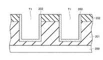
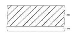
[第1の実施の形態] 図1は、本発明の第1の実施の形態に係る半導体装置の配線部の断面構造を示している。この半導体装置では、半導体基板200上に層間絶縁膜(201、202)が形成され、この層間絶縁膜に配線溝T1を形成し、この配線溝T1内に、バリアメタル膜203を介して、ダマシン法によりCu配線(205、206)が形成されている。なお、図示は省略するが、Cu配線の上面はSiN等からなるキャップ層が形成され、上層の層間絶縁膜と隔離される。この実施の形態の層間絶縁膜は、第1の層間絶縁膜201と、第2の層間絶縁膜202との少なくとも2層構造を有している。
第1の層間絶縁膜201は、Si、O、N、F、C、H、B、Pの一部又はすべての元素を含んだ絶縁膜であり、例えばSiOC系等の無機化合物膜又は有機化合物膜から形成される。この第1の層間絶縁膜201は、単層で形成してもよいし、別膜を組み合わせた積層膜としてもよい。
また、第2の層間絶縁膜202は、第1の層間絶縁膜201に比べ銅の拡散を防止する性質が高い膜、例えばSiN、SiC、SiCN等を主成分として構成される。第2の層間絶縁膜202は、例えばプラズマCVD法により第1の層間絶縁膜201上に形成される。
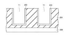
この実施の形態では、Cu配線を埋め込むための配線溝T1が、この2つの層間絶縁膜201、202を貫通するように形成される。そして、Cu配線を形成する銅が層間絶縁膜201へ拡散することを防止するバリアメタル膜203が、この配線溝T1の内壁に形成される。ただし、この実施の形態では、バリアメタル膜203は、配線溝T1の内壁の上端部を除く部分、具体的には第2の層間絶縁膜202の中間付近より上方の部分を除く部分に形成される。バリアメタル膜203を構成する材料は、例えばTa、TaN、TaSiN、Ti、TiN、Mn、MnO、Nb、NbN、WN、又はWSiN等の中から選択される。
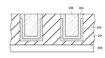
Cu配線は、この配線溝T1内に、バリアメタル膜203を介してダマシン法により埋め込まれる。この実施の形態では、Cu配線は、配線溝T1の内壁に沿って形成される第1のCu配線層205と、その第1のCu配線層205の内部に形成される第2のCu配線層206とからなっている。
第1のCu配線層205は、ECP法(Electrochemical plating)で第2のCu配線層206を形成する場合の下地層として機能するものである。第2のCu配線層206をCVD法、PVD法、無電解メッキ法等で形成する場合には、この第1のCu配線層205は省略することも可能である。
第2のCu配線層206は、第1のCu配線層205の内側の凹部を含めた半導体基板上の全体に、PVD法、CVD法、無電解メッキ法、電解メッキ法その他の手法により堆積され、第1のCu配線層205の内側の凹部に埋め込まれる。
上述のように、本実施の形態のバリアメタル膜203は配線溝T1の内壁の上端部を除く部分に形成されるため、配線溝T1に形成されるCu配線(205、206)は、配線溝T1の上端部において、第2の層間絶縁膜202とのみ接している。即ち、Cu配線(205、206)は、配線溝T1の内壁の上端部を除く部分においてバリアメタル膜203により覆われており、第1の層間絶縁膜201とは、バリアメタル膜203により隔離されている。
次に、この図1に示す配線構造の製造工程を、図2〜図9を参照して説明する。はじめに、図2に示すように、半導体基板200上に第1の層間絶縁膜201をプラズマCVD法又は塗布法により形成し、続いてこの第1の層間絶縁膜201上にCuの拡散を防止する性質を有する第2の層間絶縁膜202(SiN、SIC、SiCN)を同様にプラズマCVD法又より形成する。
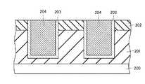
次に、第2の層間絶縁膜202上にフォトレジストを成膜してフォトリソグラフィ法によりパターンを形成する。その後、このパターニングされたフォトレジストをマスクとしてRIE法(Reactive Ion Etching )により、図3に示すような配線溝T1を形成する。その後、図4に示すように、この配線溝T1の内壁全体に、Cu配線中のCuを第1の層間絶縁膜201中に拡散させることを防止するためのバリアメタル膜203を形成する。
続いて、図5に示すように、半導体基板200上の全体に、配線溝T1の内部も含めてフォトレジスト204を堆積させた後、CMP法(Chemical Mechanical Polishing )を実行し、配線溝T1外のフォトレジスト204を除去し、配線溝T1の内部をフォトレジスト204で埋め込む。この状態において、バリアメタル203は、配線溝T1の上端部のみにおいて表面に露出している。
次に、このフォトレジスト204をマスクとしてRIE法を実行し、バリアメタル膜203の上端部を、第2の層間絶縁膜202の中間付近で、第1の層間絶縁膜201との界面まで達しない程度にまでエッチングする(図6参照)。
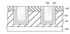
その後、図7に示すようにフォトレジスト204をプラズマエッチングを実行して剥離した後、図8に示すように、ECP法を用いて第1のCu配線層205を、配線溝T1の内壁に沿って、配線溝T1の内部に凹部を残した状態に成膜する。そして、この凹部も含めた半導体基板200の表面全体に、第2のCu配線層206を、PVD法、CVD法、無電解メッキ法、電解メッキ法その他の手法により堆積し、第1のCu配線層205の内側の凹部に埋め込む。なお、このとき堆積されている第1のCu配線層205と第2のCu配線層206との合計の膜厚は、最終的に配線形状として残る膜の膜厚以上とする。その後、CMP法にて第1のCu配線層205及び第2のCu配線層206を平坦化し、図9に示すようなCu配線又はビアホールが完成する。
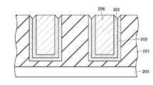
本実施の形態では、図6で説明したように、バリアメタル膜203の上端部を第2の層間絶縁膜202の中間付近までエッチバックすることにより、いわゆる電池効果による影響を無くし、低抵抗で信頼性の高いCu配線を提供することを可能にしている。このことを、図10、図11に示す参考形態との比較において説明する。図10では、層間絶縁膜201に形成された配線溝に、バリアメタル膜203を成膜した後、Cu配線層205、206を形成する点で本実施の形態と同様であるが、図6で説明したバリアメタル膜203の上端部をエッチバックする工程を実行していない。このため、バリアメタル膜203は、図10に示すように、配線溝の上端部や外部にも残存している。この状態において、Cu配線の平坦化のためにCMP法を実行すると、バリアメタル膜203とCu配線層205,206との間に電池効果が発生する。電池効果は、CMPスラリとの化学反応により、バリアメタルとCu配線層の接合部を中心として膜の溶解が生じる現象である。このため、図11に示すように、Cu配線層205、バリアメタル膜203の上端部が溶解し、凹みが生じる。この凹みは、配線抵抗及びビアホール抵抗を増大させる原因となり得る。また、配線の信頼性劣化の問題も生じる。この点、本実施の形態では、バリアメタル膜203が上記のように上端部においてエッチバックされており、配線層205,206と共にCMP除去されないため、電池効果は生じない。従って、配線抵抗やビアホール抵抗の増大を防ぎ、配線の信頼性を高く維持することができる。
[第2の実施の形態] 次に、本発明の第2の実施の形態の半導体装置の製造方法を、図12〜図21を参照して説明する。この実施の形態では、層間絶縁膜201のみに配線溝T1を形成してCu配線を形成し、第2の層間絶縁膜202はその後形成する点で第1の実施の形態の製造工程と異なっている。以下、図面を参照して説明する。
まず図12に示すように、半導体基板200上に第1の層間絶縁膜201をプラズマCVD法又は塗布法により形成する。次に、第1の層間絶縁膜201上にフォトレジストを成膜してフォトリソグラフィ法によりパターンを形成する。その後、このパターニングされたフォトレジストをマスクとしてRIE法(Reactive Ion Etching )により、図13に示すような配線溝T1を形成する。
その後、図14に示すように、この配線溝T1の内壁全体に、Cu配線中のCuを第1の層間絶縁膜201中に拡散させることを防止するためのバリアメタル膜203を形成する。続いて、図15に示すように、半導体基板200上の全体に、配線溝T1の内部も含めてフォトレジスト204を堆積させた後、CMP法(Chemical Mechanical Polishing )を実行して、配線溝T1外のフォトレジスト204を除去し、配線溝T1の内部をフォトレジスト204で埋め込む。この状態において、バリアメタル203は、配線溝T1の上端部のみにおいて表面に露出している。
その後、図14に示すように、この配線溝T1の内壁全体に、Cu配線中のCuを第1の層間絶縁膜201中に拡散させることを防止するためのバリアメタル膜203を形成する。続いて、図15に示すように、半導体基板200上の全体に、配線溝T1の内部も含めてフォトレジスト204を堆積させた後、CMP法(Chemical Mechanical Polishing )を実行して、配線溝T1外のフォトレジスト204を除去し、配線溝T1の内部をフォトレジスト204で埋め込む。この状態において、バリアメタル203は、配線溝T1の上端部のみにおいて表面に露出している。
次に、このフォトレジスト204をマスクとしてRIE法を実行し、バリアメタル膜203の上端部をエッチバックする(図16参照)。そして、フォトレジスト204をプラズマエッチングを実行して剥離した後、図17に示すように、ECP法を用いて第1の配線層205を、配線溝T1の内壁に沿って、配線溝T1の内部に凹部を残した状態に成膜する。そして、図18に示すように、この凹部も含めた半導体基板200の表面全体に、第2のCu配線層206を、PVD法、CVD法、無電解メッキ法、電解メッキ法その他の手法により堆積し、第1のCu配線層205の内側の凹部に埋め込む。なお、このとき堆積されている第1のCu配線層205と第2のCu配線層206との合計の膜厚は、最終的に配線形状として残る膜の膜厚以上とする。その後、CMP法にて第1のCu配線層205及び第2のCu配線層206を平坦化する(図19)。この状態では、Cu配線層205が第1の層間絶縁膜201と接しており、銅拡散の虞がある。そこでこの実施の形態では、図20に示すように、第1の層間絶縁膜201を、バリアメタル膜203が外部に露出し、Cu配線層205,206が第1の層間絶縁膜201と隔離されるまでエッチバックする。このとき第1の層間絶縁膜201がSiOx系の膜であれば、HF系のウエットエッチングによってエッチバックしてもよい。そして、図21に示すように、第2の層間絶縁膜210としてのSiN、SiC又はSiCNを、基板表面全体に亘って成膜する。この工程においても、図19のCMP工程においてバリアメタル膜とCu配線層とは同時に平坦化されないので、電池効果は生じず、第1の実施の形態と同様の効果を得ることができる。
以上、発明の実施の形態を説明したが、本発明はこれらに限定されるものではなく、発明の趣旨を逸脱しない範囲内において様々な変形、置換、追加等が可能である。
200・・・半導体基板、 201・・・第1の層間絶縁膜、 202、210・・・第2の層間絶縁膜、 203・・・バリアメタル膜、 204・・・フォトレジスト、 205・・・第1のCu配線層、 206・・・第2のCu配線層。
Claims (5)
- 層間絶縁膜に形成された配線溝に銅を埋め込んだ後平坦化して形成されたCu配線を具備する半導体装置において、
前記層間絶縁膜が、第1の層間絶縁膜と、前記第1の層間絶縁膜上に形成され銅の拡散を防止する性質を有する第2の層間絶縁膜とから構成され、
前記配線溝の内壁の第2の層間絶縁膜の中間付近より上方の部分を除く部分に形成されたバリアメタル膜を備え、
前記Cu配線は、前記配線溝の内壁に沿って前記バリアメタル膜上に形成され、前記配線溝上端部で前記バリアメタル膜の上端を覆い前記第2の層間絶縁膜と接するとともに、前記配線溝の内部に凹部を残して形成された第1のCu配線と、前記凹部を含む前記配線溝を埋め込むように形成された第2のCu配線とから構成される
ことを特徴とする半導体装置。 - 前記バリアメタル膜は、Ta、TaN、TaSiN、Ti、TiN、Mn、MnO、Nb、NbN、WN又はWSiNから構成されることを特徴とする請求項1記載の半導体装置。
- 前記第2の層間絶縁膜は、SiN、SiC又はSiCNを主成分とすることを特徴とする請求項1記載の半導体装置。
- 層間絶縁膜に配線溝を形成し、メタルを埋め込み平坦化して形成されたCu配線を有する半導体装置の製造方法において、
第1の層間絶縁膜を形成する工程と、
前記第1の層間絶縁膜上に銅の拡散を防止する性質を有する第2の層間絶縁膜を形成する工程と、
前記第2の層間絶縁膜を貫通して前記第1の層間絶縁膜に達するように配線溝を形成する工程と、
前記配線溝の内壁にバリアメタル膜を形成する工程と、
前記配線溝内にレジストを埋め込んだ後、このレジストをマスクとして前記バリアメタル膜を前記第1及び第2の層間絶縁膜の界面が露出しない程度までエッチバックする工程と、
前記レジストを剥離した後、前記配線溝内に銅を埋め込む工程と
を備えたことを特徴とした半導体装置の製造方法。 - 層間絶縁膜に配線溝を形成し、メタルを埋め込み平坦化して形成されたCu配線を有する半導体装置の製造方法において、
第1の層間絶縁膜を形成する工程と、
前記第1の層間絶縁膜に配線溝を形成する工程と、
前記配線溝の内壁にバリアメタル膜を形成する工程と、
前記バリアメタル膜上にレジストを埋め込んだ後、このレジストをマスクとして前記バリアメタル膜をエッチバックする工程と、
前記レジストを剥離した後前記Cu配線を前記配線溝に埋め込み形成する工程と、
前記第1の層間絶縁膜を前記バリアメタル膜が露出する程度までエッチバックする工程と、
前記第1の層間絶縁膜及び前記Cu配線を覆うように銅の拡散を防止する性質を有する第2の層間絶縁膜を形成する工程と
を備えたことを特徴とした半導体装置の製造方法。
Priority Applications (2)
| Application Number | Priority Date | Filing Date | Title |
|---|---|---|---|
| JP2006028053AJP4231055B2 (ja) | 2006-02-06 | 2006-02-06 | 半導体装置及びその製造方法 |
| US11/702,135US7553757B2 (en) | 2006-02-06 | 2007-02-05 | Semiconductor device and method of manufacturing the same |
Applications Claiming Priority (1)
| Application Number | Priority Date | Filing Date | Title |
|---|---|---|---|
| JP2006028053AJP4231055B2 (ja) | 2006-02-06 | 2006-02-06 | 半導体装置及びその製造方法 |
Publications (2)
| Publication Number | Publication Date |
|---|---|
| JP2007208170A JP2007208170A (ja) | 2007-08-16 |
| JP4231055B2true JP4231055B2 (ja) | 2009-02-25 |
Family
ID=38443193
Family Applications (1)
| Application Number | Title | Priority Date | Filing Date |
|---|---|---|---|
| JP2006028053AExpired - Fee RelatedJP4231055B2 (ja) | 2006-02-06 | 2006-02-06 | 半導体装置及びその製造方法 |
Country Status (2)
| Country | Link |
|---|---|
| US (1) | US7553757B2 (ja) |
| JP (1) | JP4231055B2 (ja) |
Cited By (1)
| Publication number | Priority date | Publication date | Assignee | Title |
|---|---|---|---|---|
| US11315926B2 (en) | 2020-06-09 | 2022-04-26 | Samsung Electronics Co., Ltd. | Integrated circuit devices and methods of manufacturing the same |
Families Citing this family (9)
| Publication number | Priority date | Publication date | Assignee | Title |
|---|---|---|---|---|
| JP2009194195A (ja)* | 2008-02-15 | 2009-08-27 | Panasonic Corp | 半導体装置及びその製造方法 |
| JP2010040771A (ja)* | 2008-08-05 | 2010-02-18 | Rohm Co Ltd | 半導体装置の製造方法 |
| US7955971B2 (en)* | 2009-06-11 | 2011-06-07 | International Business Machines Corporation | Hybrid metallic wire and methods of fabricating same |
| KR101604054B1 (ko)* | 2009-09-03 | 2016-03-16 | 삼성전자주식회사 | 반도체 소자 및 그 형성방법 |
| KR102274775B1 (ko) | 2014-11-13 | 2021-07-08 | 삼성전자주식회사 | 반도체 장치 및 그 제조 방법 |
| US10096639B2 (en)* | 2016-10-10 | 2018-10-09 | Sensors Unlimited, Inc. | Bump structures for interconnecting focal plane arrays |
| DE102018102448B4 (de) | 2017-11-30 | 2023-06-15 | Taiwan Semiconductor Manufacturing Co., Ltd. | Bildung und Struktur leitfähiger Merkmale |
| US10361120B2 (en) | 2017-11-30 | 2019-07-23 | Taiwan Semiconductor Manufacturing Co., Ltd. | Conductive feature formation and structure |
| CN116230623A (zh)* | 2023-03-22 | 2023-06-06 | 上海华力集成电路制造有限公司 | 改善铜互连技术的经时介电层击穿性能的方法 |
Family Cites Families (17)
| Publication number | Priority date | Publication date | Assignee | Title |
|---|---|---|---|---|
| JP3373320B2 (ja) | 1995-02-10 | 2003-02-04 | 株式会社アルバック | 銅配線製造方法 |
| JP3521200B2 (ja) | 1995-12-12 | 2004-04-19 | 松下電器産業株式会社 | 配線構造およびその形成方法 |
| US5994220A (en)* | 1996-02-02 | 1999-11-30 | Micron Technology, Inc. | Method for forming a semiconductor connection with a top surface having an enlarged recess |
| US6124203A (en)* | 1998-12-07 | 2000-09-26 | Advanced Micro Devices, Inc. | Method for forming conformal barrier layers |
| JP2000323479A (ja) | 1999-05-14 | 2000-11-24 | Sony Corp | 半導体装置およびその製造方法 |
| US6433429B1 (en)* | 1999-09-01 | 2002-08-13 | International Business Machines Corporation | Copper conductive line with redundant liner and method of making |
| FR2802336B1 (fr)* | 1999-12-13 | 2002-03-01 | St Microelectronics Sa | Structure d'interconnexions de type damascene et son procede de realisation |
| US20020081845A1 (en)* | 2000-12-27 | 2002-06-27 | Novellus Systems, Inc. | Method for the formation of diffusion barrier |
| JP2003007705A (ja) | 2001-06-26 | 2003-01-10 | Mitsubishi Electric Corp | 銅配線の形成方法 |
| US6734090B2 (en)* | 2002-02-20 | 2004-05-11 | International Business Machines Corporation | Method of making an edge seal for a semiconductor device |
| US7687917B2 (en)* | 2002-05-08 | 2010-03-30 | Nec Electronics Corporation | Single damascene structure semiconductor device having silicon-diffused metal wiring layer |
| JP4076131B2 (ja)* | 2002-06-07 | 2008-04-16 | 富士通株式会社 | 半導体装置の製造方法 |
| US6964919B2 (en)* | 2002-08-12 | 2005-11-15 | Intel Corporation | Low-k dielectric film with good mechanical strength |
| JP3949652B2 (ja)* | 2003-02-17 | 2007-07-25 | Necエレクトロニクス株式会社 | 半導体装置の製造方法 |
| JP3647853B1 (ja) | 2003-10-24 | 2005-05-18 | 沖電気工業株式会社 | 半導体装置の配線構造及びその製造方法 |
| KR100552812B1 (ko)* | 2003-12-31 | 2006-02-22 | 동부아남반도체 주식회사 | 반도체 소자의 구리 배선 형성 방법 |
| US7432189B2 (en)* | 2005-11-30 | 2008-10-07 | Lam Research Corporation | Device with self aligned gaps for capacitance reduction |
- 2006
- 2006-02-06JPJP2006028053Apatent/JP4231055B2/janot_activeExpired - Fee Related
- 2007
- 2007-02-05USUS11/702,135patent/US7553757B2/ennot_activeExpired - Fee Related
Cited By (2)
| Publication number | Priority date | Publication date | Assignee | Title |
|---|---|---|---|---|
| US11315926B2 (en) | 2020-06-09 | 2022-04-26 | Samsung Electronics Co., Ltd. | Integrated circuit devices and methods of manufacturing the same |
| US11646316B2 (en) | 2020-06-09 | 2023-05-09 | Samsung Electronics Co., Ltd. | Integrated circuit devices and methods of manufacturing the same |
Also Published As
| Publication number | Publication date |
|---|---|
| US20070200237A1 (en) | 2007-08-30 |
| JP2007208170A (ja) | 2007-08-16 |
| US7553757B2 (en) | 2009-06-30 |
Similar Documents
| Publication | Publication Date | Title |
|---|---|---|
| JP4231055B2 (ja) | 半導体装置及びその製造方法 | |
| JP5089575B2 (ja) | 相互接続構造体及びその製造方法 | |
| KR100442863B1 (ko) | 금속-절연체-금속 커패시터 및 다마신 배선 구조를 갖는반도체 소자의 제조 방법 | |
| JP4918778B2 (ja) | 半導体集積回路装置の製造方法 | |
| JP2006019480A (ja) | 半導体装置の製造方法 | |
| EP2047506B1 (en) | Process for making an interconnect structure | |
| JP2008294335A (ja) | 半導体装置の製造方法 | |
| JP2010080774A (ja) | 半導体装置 | |
| KR20060082694A (ko) | 이중 확산방지막을 갖는 배선구조 및 그 제조방법 | |
| JP2007294625A (ja) | 半導体装置の製造方法 | |
| JP4272168B2 (ja) | 半導体装置及び半導体集積回路装置 | |
| US6878621B2 (en) | Method of fabricating barrierless and embedded copper damascene interconnects | |
| JP5047504B2 (ja) | ビアキャッピング保護膜を使用する半導体素子のデュアルダマシン配線の製造方法 | |
| JP4646591B2 (ja) | 半導体装置及びその製造方法 | |
| JP2009272563A (ja) | 半導体装置及びその製造方法 | |
| JP2010080773A (ja) | 半導体装置 | |
| JP2006216787A (ja) | 半導体装置およびその製造方法 | |
| US20040192008A1 (en) | Semiconductor device including interconnection and capacitor, and method of manufacturing the same | |
| JP2007335578A (ja) | 半導体装置及びその製造方法 | |
| KR100781422B1 (ko) | 듀얼 다마신 패턴 형성 방법 | |
| JP4383262B2 (ja) | 半導体装置及びその製造方法 | |
| JP2002319617A (ja) | 半導体装置及びその製造方法 | |
| US8048799B2 (en) | Method for forming copper wiring in semiconductor device | |
| JP2010016236A (ja) | 半導体装置の製造方法 | |
| JP5424551B2 (ja) | 半導体装置 |
Legal Events
| Date | Code | Title | Description |
|---|---|---|---|
| A131 | Notification of reasons for refusal | Free format text:JAPANESE INTERMEDIATE CODE: A131 Effective date:20080826 | |
| A977 | Report on retrieval | Free format text:JAPANESE INTERMEDIATE CODE: A971007 Effective date:20080828 | |
| A521 | Request for written amendment filed | Free format text:JAPANESE INTERMEDIATE CODE: A523 Effective date:20081027 | |
| TRDD | Decision of grant or rejection written | ||
| A01 | Written decision to grant a patent or to grant a registration (utility model) | Free format text:JAPANESE INTERMEDIATE CODE: A01 Effective date:20081202 | |
| A01 | Written decision to grant a patent or to grant a registration (utility model) | Free format text:JAPANESE INTERMEDIATE CODE: A01 | |
| A61 | First payment of annual fees (during grant procedure) | Free format text:JAPANESE INTERMEDIATE CODE: A61 Effective date:20081204 | |
| FPAY | Renewal fee payment (event date is renewal date of database) | Free format text:PAYMENT UNTIL: 20111212 Year of fee payment:3 | |
| LAPS | Cancellation because of no payment of annual fees |