JP4230768B2 - Data carrier designed for non-contact communication and having detection means for detecting the main temperature of the data carrier - Google Patents
Data carrier designed for non-contact communication and having detection means for detecting the main temperature of the data carrierDownload PDFInfo
- Publication number
- JP4230768B2 JP4230768B2JP2002543372AJP2002543372AJP4230768B2JP 4230768 B2JP4230768 B2JP 4230768B2JP 2002543372 AJP2002543372 AJP 2002543372AJP 2002543372 AJP2002543372 AJP 2002543372AJP 4230768 B2JP4230768 B2JP 4230768B2
- Authority
- JP
- Japan
- Prior art keywords
- data carrier
- integrated circuit
- circuit
- data
- temperature
- Prior art date
- Legal status (The legal status is an assumption and is not a legal conclusion. Google has not performed a legal analysis and makes no representation as to the accuracy of the status listed.)
- Expired - Fee Related
Links
Images


Classifications
- G—PHYSICS
- G06—COMPUTING OR CALCULATING; COUNTING
- G06K—GRAPHICAL DATA READING; PRESENTATION OF DATA; RECORD CARRIERS; HANDLING RECORD CARRIERS
- G06K7/00—Methods or arrangements for sensing record carriers, e.g. for reading patterns
- G06K7/08—Methods or arrangements for sensing record carriers, e.g. for reading patterns by means detecting the change of an electrostatic or magnetic field, e.g. by detecting change of capacitance between electrodes
- G—PHYSICS
- G06—COMPUTING OR CALCULATING; COUNTING
- G06K—GRAPHICAL DATA READING; PRESENTATION OF DATA; RECORD CARRIERS; HANDLING RECORD CARRIERS
- G06K19/00—Record carriers for use with machines and with at least a part designed to carry digital markings
- G06K19/06—Record carriers for use with machines and with at least a part designed to carry digital markings characterised by the kind of the digital marking, e.g. shape, nature, code
- G06K19/067—Record carriers with conductive marks, printed circuits or semiconductor circuit elements, e.g. credit or identity cards also with resonating or responding marks without active components
- G06K19/07—Record carriers with conductive marks, printed circuits or semiconductor circuit elements, e.g. credit or identity cards also with resonating or responding marks without active components with integrated circuit chips
- G06K19/077—Constructional details, e.g. mounting of circuits in the carrier
- G06K19/0772—Physical layout of the record carrier
- G06K19/0773—Physical layout of the record carrier the record carrier comprising means to protect itself against external heat sources
- G—PHYSICS
- G06—COMPUTING OR CALCULATING; COUNTING
- G06K—GRAPHICAL DATA READING; PRESENTATION OF DATA; RECORD CARRIERS; HANDLING RECORD CARRIERS
- G06K19/00—Record carriers for use with machines and with at least a part designed to carry digital markings
- G06K19/06—Record carriers for use with machines and with at least a part designed to carry digital markings characterised by the kind of the digital marking, e.g. shape, nature, code
- G06K19/067—Record carriers with conductive marks, printed circuits or semiconductor circuit elements, e.g. credit or identity cards also with resonating or responding marks without active components
- G06K19/07—Record carriers with conductive marks, printed circuits or semiconductor circuit elements, e.g. credit or identity cards also with resonating or responding marks without active components with integrated circuit chips
- G06K19/0701—Record carriers with conductive marks, printed circuits or semiconductor circuit elements, e.g. credit or identity cards also with resonating or responding marks without active components with integrated circuit chips at least one of the integrated circuit chips comprising an arrangement for power management
- G—PHYSICS
- G06—COMPUTING OR CALCULATING; COUNTING
- G06K—GRAPHICAL DATA READING; PRESENTATION OF DATA; RECORD CARRIERS; HANDLING RECORD CARRIERS
- G06K19/00—Record carriers for use with machines and with at least a part designed to carry digital markings
- G06K19/06—Record carriers for use with machines and with at least a part designed to carry digital markings characterised by the kind of the digital marking, e.g. shape, nature, code
- G06K19/067—Record carriers with conductive marks, printed circuits or semiconductor circuit elements, e.g. credit or identity cards also with resonating or responding marks without active components
- G06K19/07—Record carriers with conductive marks, printed circuits or semiconductor circuit elements, e.g. credit or identity cards also with resonating or responding marks without active components with integrated circuit chips
- G06K19/0723—Record carriers with conductive marks, printed circuits or semiconductor circuit elements, e.g. credit or identity cards also with resonating or responding marks without active components with integrated circuit chips the record carrier comprising an arrangement for non-contact communication, e.g. wireless communication circuits on transponder cards, non-contact smart cards or RFIDs
- G06K19/0726—Record carriers with conductive marks, printed circuits or semiconductor circuit elements, e.g. credit or identity cards also with resonating or responding marks without active components with integrated circuit chips the record carrier comprising an arrangement for non-contact communication, e.g. wireless communication circuits on transponder cards, non-contact smart cards or RFIDs the arrangement including a circuit for tuning the resonance frequency of an antenna on the record carrier
Landscapes
- Engineering & Computer Science (AREA)
- Computer Hardware Design (AREA)
- Microelectronics & Electronic Packaging (AREA)
- Physics & Mathematics (AREA)
- General Physics & Mathematics (AREA)
- Theoretical Computer Science (AREA)
- Computer Networks & Wireless Communication (AREA)
- Artificial Intelligence (AREA)
- Computer Vision & Pattern Recognition (AREA)
- Near-Field Transmission Systems (AREA)
- Measuring Temperature Or Quantity Of Heat (AREA)
- Dc Digital Transmission (AREA)
Abstract
Description
Translated fromJapanese【0001】
【発明の属する技術分野】
本発明は、当該データキャリア用に設計されている通信局と非接触通信を行うデータキャリア、当該通信局用に設計されているデータキャリアと非接触通信を行う通信局、及び当該データキャリア用に設計されている通信局と非接触通信を行うデータキャリア用の集積回路に関する。
【0002】
【従来の技術】
斯様なデータキャリア、斯様な集積回路及び斯様な通信局は、例えば、国際特許出願公開第WO99/57681 A1号公報に記載され、故に既知である。既知のデータキャリアは集積回路を持ち、該集積回路を用いて、他の回路セクションの他に、直流電圧生成回路が実現される。この回路は、整流段を含み、更に電圧制限手段を含む。電圧制限手段により、直流電圧生成回路により生成され得る直流供給電圧を、必要な時に、最大値に制限することができる。斯様な制限は、例えば、データキャリアが通信局の近くに位置する、したがって、該通信局により生成され得る通信フィールドの高いフィールド強度を持つ領域に位置する場合に必要である。なぜなら、電圧制限手段がない場合、高いフィールド強度は、直流電圧生成回路の出力に過大な直流供給電圧を生ぜしめるであろうからである。直流電圧生成回路の動作、とりわけ、電圧制限手段の動作は、既知のデータキャリア内で発熱を招く。この結果、既知のデータキャリア内で温度上昇が生じる。斯様な温度上昇は、直流電圧生成回路及び電圧制限回路の両方を実現する集積回路が比較的大きな表面積を持ち、故に、比較的大きな温度上昇に対処することができる場合にはあまり重要ではない結果にしかならない。しかしながら、斯様な温度上昇は、通信局と非接触通信を提供するように構成されているデータキャリア用の集積回路が、上述した従来技術の解決策の場合におけるよりも高度に小型化されている場合に問題となる。なぜなら、斯様な温度上昇の結果、集積回路が少なくとも部分的に、過度に高い温度に起因して損傷を受けたり、まして壊れてしまう危険性があるからである。
【0003】
【発明が解決しようとする課題】
本発明の目的は、データキャリア及び集積回路の更なる小型化の場合におけるデータキャリア及び集積回路に対する悪影響の危険性を、本発明による対策の備えがない場合データキャリア及び集積回路における所与の許容可能な動作温度の範囲外に至るであろう、比較的大きな温度変化が動作中に生じるような動作状態においてさえ防止することにある。
【0004】
【課題を解決するための手段】
上述の目的を達成するために、本発明によるデータキャリアが、以下に規定されるように、即ち、通信局と非接触通信を提供するように構成されるデータキャリアであって、集積回路と、当該データキャリア用の直流供給電圧を生成し、供給するように作用する直流電圧生成回路と、当該データキャリア内の検出手段の環境の主温度を検出する検出手段であって、該検出手段を用いて、前記主温度を表す表示信号(representation signal)が生成され得る、検出手段と、前記表示信号を受信し、処理するように構成され、当該データキャリアにおける温度の変化を開始するように構成される開始手段(initiation means)とを含むことを特徴とするようにして、本発明による特徴的なフィーチャが、本発明によるデータキャリアに備えられる。
【0005】
上述の目的を達成するために、本発明による集積回路が、通信局と非接触通信を提供するデータキャリア用の集積回路であって、当該集積回路用の直流供給電圧を生成し、供給するように作用する直流電圧生成回路と、当該集積回路内の検出手段の環境の主温度を検出する検出手段であって、該検出手段を用いて、前記主温度を表す表示信号が生成され得る、検出手段と、前記表示信号を受信し、処理するように構成され、当該集積回路における温度の変化を開始するように構成される開始手段とを含むことを特徴とするようにして、本発明による特徴的なフィーチャが、本発明による集積回路に備えられる。
【0006】
本発明による特徴的フィーチャを備える結果、比較的簡単に且つ低コストの追加しかないようにして、データキャリア及び斯様なデータキャリア用の集積回路内の温度が、該データキャリア及び該集積回路内の動作温度を所要の特定の動作温度の範囲内に保つように、状況に依存して変化され得る、即ち、上昇又は低下され得る、と言うことが達成される。
【0007】
本発明によるデータキャリア及び本発明による集積回路において、開始手段は、温度の上昇を開始するように構成されても良い。これは、例えば、本発明によるデータキャリア及び本発明による集積回路が凍結環境において正しく動作すべきであるような場合に要求されるかもしれない。しかしながら、開始手段が、データキャリア及び集積回路内の温度の低下を開始するように構成される場合にとりわけ有利であることが証明された。これは、データキャリア及び斯様なデータキャリア用の集積回路の使用の多くにおいて、比較的強い発熱が、とりわけ集積回路が最小のチップ面積上に実現されるべき場合に生じる恐れがあり、この場合、望ましくない温度上昇が、本発明による対策を用いて防止されると言う点でとりわけ有利である。
【0008】
本発明によるデータキャリア及び本発明による集積回路において、入力回路の入力抵抗を用いて温度に影響を与えることができる。なぜなら、温度変化、例えば、温度上昇があり得る動作範囲においてデータキャリアが受け、更に該データキャリアにより処理されるエネルギは、入力回路の入力抵抗に比例し、故に、エネルギ入力を、該入力抵抗を変化させることにより変化させることができ、これが、該データキャリア及び該集積回路内の温度の変化をもたらすからである。
【0009】
本発明によるデータキャリア及び本発明による集積回路において、可能な限りにおいて温度を変化させるため、通信局により該データキャリアに送信される通信信号を受信するために斯様なデータキャリアに設けられる送信共振回路を用いることも可能である。なぜなら、斯様な送信共振回路によるエネルギ入力は、該送信共振回路の共振周波数に依存し、この結果、データキャリアへのエネルギ入力を、送信共振回路の共振周波数を変化させることにより比較的簡単に変化させることができ、これが、データキャリア及びその集積回路の主温度の変化を招くからである。送信共振回路の共振周波数を変化させるために、該送信共振回路内に又該送信共振回路外に切り換えられ得るコンデンサを用いることが可能である。共振周波数を変えることは、他の例においては、インダクタを前記回路内に又は外に切り換えることによりなされても良い。
【0010】
しかしながら、本発明によるデータキャリア及び本発明による集積回路を用いると、開始手段が、データキャリアから通信局への、該データキャリア及び該集積回路の主温度を表す表示信号に対応する送信信号の送信を支援するように適合される場合に非常に有利であることも証明された。この実施例は、データキャリア及び集積回路の主温度の変化が、該データキャリア及び該集積回路において開始されるが、該データキャリア及び該集積回路における温度を変化させる手段が、該データキャリア又は該集積回路に含まれず、該データキャリア及び該集積回路と非接触通信を提供するように構成される通信局に含まれると言う利点を持つ。
【0011】
これに関連して、本発明による通信局が、データキャリアにより送信され該通信局により受信される送信信号を処理する局処理手段を含み、該局処理手段により影響を及ぼされ得る制御手段を更に含み、該制御手段を用いて、該通信局から該データキャリアに送信される通信信号のエネルギコンテンツが変化され得る場合に非常に有利であることが証明された。これは、本発明によるデータキャリア及び本発明による集積回路における温度を変化させるための対策が、本発明による通信局において実施されると言う利点を持ち、これは、必要とされるならば、データキャリア及び集積回路における温度を変化させるためのかなり高価でかなり複雑な手段を、比較的安価に実現することができると言う利点を持つ。
【0012】
本発明の上述の及び他の特徴が、例として以下に記載される実施例から明らかになり、これらの例を参照して詳述されるであろう。
【0013】
ここでは、本発明は、四つの実施例を示す図を参照してより詳細に述べられるが、これらは、例として与えられているものであり、本発明を限定するものではない。
【0014】
【発明の実施の形態】
図1は、通信局2と非接触通信を提供するように構成されるデータキャリア1を示す。
【0015】
通信局2は、局制御ユニットを含む局データ処理装置3を含む。これは、マイクロコンピュータにより実現されるが、他の例においては、配線された論理回路により形成されても良い。通信局2は更に、局データ処理装置3に接続される送受信手段4を含む。この結果、局データ処理装置3から送受信手段4に及び送受信手段4から局データ処理装置3にデータを送信することが可能である。通信局2は更に、局送信コイル5を含む。局送信コイル5は、送受信手段4に接続され、局送信コイル5を用いて、データキャリア1の送信コイルとの非接触通信が可能であり、この非接触通信は、誘導的になされる。
【0016】
データキャリア1は、送信コイル6を持つ。送信コイル6は、通信局2の局送信コイル5と誘導的に協働するように作用し、且つ通信局2の局送信コイル5と誘導的に協働するように構成される。データキャリア1は更に、集積回路7を含む。集積回路7は、第1の端子8及び第2の端子9を持つ。送信コイル6は、二つの端子8及び9に接続されている。集積回路7は、二つの端子8及び9に並列に配設されるコンデンサ10を含む。コンデンサ10は、送信共振回路11のメインコンポーネント(main component)を形成する。送信共振回路11は、通信信号AMCSを受信するように作用する。通信信号AMCSは振幅変調通信信号である。送信共振回路11は、共振周波数に同調される。共振周波数は、既知のように、通信局2において生成され得る、データ送信の目的のために振幅変調される(この結果、振幅変調通信信号AMCSが形成される)キャリア信号の周波数に少なくとも実質的に対応する。
【0017】
集積回路7は、送信コイル6に接続される振幅復調手段を含む。振幅復調手段12は、受信した振幅変調通信信号AMCSが復調されることを可能にし、該振幅復調手段12は、復調後復調通信信号DCSを供給する。集積回路7は更に、復号手段13を含む。復号手段13は、振幅復調手段12の後に配設され、該復号手段13には、復調通信号信号DCSが供給され得る。復号手段13は、この信号を復号し、この結果、復号信号DSを供給することができる。
【0018】
集積回路7は更に、データ処理装置14を含む。データ処理装置14は、マイクロコンピュータを用いて実現されるが、他の例においては、配線論理回路により実現されても良い制御ユニット(図示せず)を含む。復号手段13により供給される復号信号は、データ処理装置14において処理されるために該データ処理装置14に供給され得る。データ処理装置14は、メモリMEMと協働し、該データ処理装置14及び該装置に含まれる制御ユニットは、メモリMEMにデータを読出し、該メモリMEMからデータが読出されることを可能にする。
【0019】
集積回路7は更に、符号化手段15を含む。符号化手段15は、データ処理装置14に接続され、該符号化手段15には、データDA、例えば、データワードDWが、該データDAを通信局2に送信するためにデータ処理装置14により供給され得る。符号化手段15は、供給データDAを符号化し、この符号化後、符号化データCDA、例えば、符号化データワードCDWを供給する。
【0020】
集積回路7は更に、制御信号生成回路16を含む。制御信号生成回路16には、符号化データCDA又はCDWが符号化手段15により供給され得る。制御信号生成回路16は、制御信号CSLを生成することができ、制御信号CSLは、該制御信号生成回路16の出力部において利用可能である。集積回路7は更に、負荷変調段17を含む。負荷変調段17は、送信共振回路11と並列に配設される。負荷変調段17は、抵抗18及び該抵抗18と直列に配設され、トランジスタにより形成されるスイッチ19を含む。スイッチ19は、制御信号生成回路16により供給される制御信号CSLを用いて制御され得る。斯くして、スイッチ19は、図1に示される非導通状態と導通状態との間で切り換えられることができ、これは、送信共振回路11の異なる負荷、従って、通信局2により生成されこの局の局送信コイル5に供給される非変調キャリア信号の負荷変調をもたらす。
【0021】
集積回路7は更に、直流電圧生成回路20を含む。直流電圧生成回路20は、データキャリア1及び集積回路7用の直流供給電圧Vを生成し、供給するように作用する。直流供給電圧Vは、この直流供給電圧を必要とする集積回路7の全ての回路素子に供給され得るが、これは、図1の明瞭さに過度に悪影響を及ぼすことのないように図示されていない。直流電圧生成回路20は、整流段21を含む。直流電圧生成回路20は更に、電圧制限回路22を含む。電圧制限回路22は、制御信号生成回路23、FETにより形成される並列制御段24及び直列制御段25からなる。FETに代えて、他のタイプのトランジスタを使用することも可能である。整流段21は、送信共振回路11と並列に配設される。整流段21は、通信局2から送信共振回路11に誘導的に送信される変調又は非変調キャリア信号によりもたらされる、送信共振回路11において作り出される電気エネルギから直流電圧を得る。この直流電圧は、制御信号生成段23及び直列制御段25の両方に供給される。制御信号生成段23は、制御信号CSBを生成する。制御信号CSBは、並列制御段24を制御するために該並列制御段24を形成するFETの制御電極に供給される。FETにより形成される並列制御段24は、入力抵抗を持つ入力回路を構成する。入力回路、即ち、並列制御段24の入力抵抗を、制御信号CSBを用いて変化させることができ、この結果、該入力抵抗を、入力段の入力抵抗を低減させることにより、即ち、FETの主電流路における抵抗を低減させることにより低減させることができる。これは、整流段21に供給されるエネルギが低減されることを可能にする。斯くして、電圧制限が、必要な場合に、制御信号生成段23及び並列段24により達成され得る。更に、直流電圧生成回路20は、直流制御段25を含む。直流制御段25は、並列制御段24を用いて達成され得るよりも微細な制御を提供する。斯様な並列制御段24及び斯様な直列制御段25の備え自体は、しばらく前より現存するデータキャリアや現存する集積回路から知られている。バッファコンデンサ27が、並列制御段25の出力部26に接続されている。生成された直流供給電圧Vは、バッファコンデンサ27間で利用可能である。
【0022】
有利には、データキャリア1及び該データキャリア1の集積回路7は、該データキャリア1及び該集積回路7内の当該検出手段28の環境の主温度を検出する検出手段28を含む。有利には、検出手段28は、直流電圧生成回路20近傍に、とりわけ、並列制御段24の近傍に配設される。なぜなら、この領域において、集積回路7及びデータキャリア1における温度上昇が、並列制御段24の強い制限作用(strong limiting action)及びその結果の供給エネルギの放散の結果として最大だからである。
【0023】
検出手段28は、温度センサ29及び該温度センサ29の後に配設されるセンサ信号処理手段を含む。温度センサ29は、定電流が印加され、そのダイオード電圧が既知の特性に従し温度に依存するダイオードを用いて簡単に実現され得る。斯くして、ダイオード電圧は、センサ信号処理手段30に供給される、温度センサ29の出力信号を表す。ダイオードに代えて、温度センサ29は、その温度依存性のベース−エミッタ電圧が温度センサ29の出力信号を形成するバイポーラトランジスタを用いて、又はそのゲート電圧が温度センサ29の出力信号を形成するCMOSトランジスタを用いても実現され得る。
【0024】
次いで、表示信号RSが、温度センサ29の出力信号に依存するセンサ信号処理手段30を用いて生成される。この表示信号は、検出手段28及び温度センサ29の環境の主温度を表す。表示信号RSは、接続部31を介して電圧制限回路22の制御信号生成段23に供給される。温度が上昇した場合、温度センサ29を用いて検出され、斯かる表示信号RSが生成され、制御信号生成段23に供給される。制御信号生成段23は、より大きな即ちより強い制御信号CSBを生成し、その結果、並列制御段24を形成するFETが、その低抵抗領域に向け駆動され、斯くして、該並列制御段24の制限作用が増大される。そして、この結果、整流段21に供給されるエネルギが制限され、集積回路7における温度上昇を相殺する。FETが低抵抗領域に向け駆動されるため並列抵抗が低減されるので、整流段21の入力電圧は、満足の行く正確な電力供給に必要とされるよりも小さくなる。しかしながら、これは、供給電圧Vでもって通電されるべき、直列制御段25の後の集積回路7の部分が、次いで、バッファコンデンサ27を介して通電され、該バッファコンデンサ27が、並列制御段24を形成するFETの制御にとりわけ必要とされる、適当な供給電圧Vを維持することを確実とするようにして補償される。バッファコンデンサ27を用いる適当な電力供給をバッファコンデンサ27の所与のキャパシタンスに対し保証する比較的長い時間を得るために、バッファコンデンサ27の不必要なローディング(loading)を回避するため、この動作状況においては必要とされない集積回路7の部分をオフすること、又はバッファコンデンサ27からの電力ドレインの低減にもなる、集積回路7のある部分のみにバッファコンデンサ26を接続することが有利である。
【0025】
ここで述べられる実施例においては、制御信号生成段23が、表示信号RSを受信し、処理するように構成され、データキャリア1及び集積回路7内の温度の変化を開始するように構成された開始手段を形成する。
【0026】
図1において一点鎖線で示されている、上述した集積回路の実施例の変形例は、開始手段32を含む。開始手段32は、制御信号生成段32に加えて、二つの更なる部分、即ち、検出手段28のセンサ信号処理手段30の後に配設されるADコンバータ28及びデータ処理装置14を用いて実施されるデータワード処理手段34を含む。この変形例においては、表示信号RSが、ADコンバータ33に供給され得る。ADコンバータ33は、AD変換を行い、データワードDWを供給する。データワードDWは、表示信号RSに対応し、データワード処理手段34に供給される。データ処理手段34は、供給されたデータワードDWを処理し、接続部35を介して制御信号生成段23に信号を供給する。この信号は、制御信号生成段23において処理され、斯くして、温度上昇が温度センサ29により検出される場合に並列制御段24を形成するFETの抵抗が低減されるようにして、制御信号生成段23により供給される制御信号CSBに影響を与える、即ち、変化させる。
【0027】
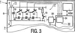
図2は、集積回路7が、送信共振回路11のメインコンポーネントとして設けられたコンデンサ10に加えて、第1の付加コンデンサ40、第2の付加コンデンサ41及び第3のコンデンサ42を含むデータキャリア1の一部のみを示している。第1のスイッチ43が、第1の付加コンデンサ40と直列に配設される。第2のスイッチ44が、第2の付加コンデンサ41と直列に配設される。第3のスイッチ45が、第3の付加コンデンサ42と直列に配設される。これら三つのスイッチ43、44及び45は、トランジスタを用いて実現される。本例の場合、これら三つのスイッチ43、44及び45は、データワード処理手段34を用いて制御され得る。斯くして、これら三つのスイッチ43、44及び45は、図2に示される非導通状態と図示されていない導通状態との間で切り換えられ得る。結果として、1つ以上の付加コンデンサ40、41及び42がコンデンサ10と並列に選択的に配設され得る。少なくとも一つの付加コンデンサを選択的に回路内に切り換えることにより、送信共振回路11の共振周波数を簡単に変化させることができる。斯くして、送信共振回路11のエネルギ吸収容量を変化させることが再び可能である。図2のデータキャリアにおける温度上昇が、図示せぬ検出手段28を用いて検出される場合、データワード処理手段34は、三つの付加コンデンサ40、41及び42の少なくとも一つを、表示信号RSの大きさに依存してコンデンサ10に接続し、この結果、送信共振回路11が通信局2を用いて生成される通信フィールドからより少ない電力を抽出可能にし、そして、データキャリア1及びその集積回路7内の温度の低下を招くようような該送信共振回路11における周波数関係の変化をもたらすことを確実にする。
【0028】
図3に示されるデータキャリア1は、図2に示されるデータキャリア1の変形例である。図3に示されるデータキャリア1も、三つの付加コンデンサ46、47及び48を含むが、本例においては、これらコンデンサは、コンデンサ10と直列に配設されている。図3に示されるデータキャリア1も、各々トランジスタにより形成される三つのスイッチ49、50及び51を含む。第1のスイッチ49は、第1の付加コンデンサ46と並列に配設される。第2のスイッチ50は、第2の付加コンデンサ47と並列に配設される。第3のスイッチ51は、第3の付加コンデンサ48と並列に配設される。これら三つのスイッチ49、50及び51は、休止状態(rest condition)において導通接続部を形成し、動作状態において非導通となる。これらは、データワード処理手段34を用いてなされる。図2及び3に示される二つのデータキャリア1、並びに図2及び図3に示される集積回路7における、図示せぬADコンバータ33及びデータワード処理手段34からなる開始手段32は、送信共振回路11の共振周波数の変化を開始する。
【0029】
図1、2及び3に示されるデータキャリア1及び図1、2及び3に示される集積回路7の何れにおいても、データキャリア1及び集積回路7内で主温度の変化の開始が、該データキャリア1及び該集積回路7において行われる。データキャリア1及び集積回路7は、該データキャリア1内で及び該集積回路7内で主温度を変化させる手段及び対策も含む。
【0030】
他の解決策が、図4に示されるようにデータキャリア1及び通信局2に対して選択されている。これを、以下でより詳細に述べる。
【0031】
図1、2及び3に示されるデータキャリア1と同様に、図4に示されるデータキャリア1は、開始手段を含む。図4に示されるデータキャリア1は、開始手段54を含む。開始手段54は、ADコンバータ33、データワード処理手段34、符号化手段15、制御信号生成回路16、負荷変調段17及び送信共振回路11からなる。ここでは、開始手段54は、表示信号RSに対応する送信信号の送信を支援するように、即ち、本例の場合、データキャリア1から、即ち、その集積回路7から通信局2への、表示信号RSに対応するデータワードDWの送信を支援するように構成される。
【0032】
上述した開始手段54以外、図4に示されるデータキャリア1は、図1に示されるデータキャリアと実質的に同様の設計のものである。
【0033】
図4に示されるデータキャリア1と協働するように作用する、図2に示される通信局2は、局データ処理装置3を含む。局データ処理装置3は、図1に示される通信局2を参照して既に述べたように、図4においても示されていない、局制御ユニットを含む。局データ処理装置3は更に、局処理手段55を含み、この機能を以下に述べる。
【0034】
通信局2は、符号化手段56を含む。符号化手段56には、局データ処理装置3により供給されるデータDAが供給され、該符号化手段56は、該データDAを符号化し、それに従って符号化されたデータCDAを供給することが可能である。データDAは、例えば、コマンドを表してもよい。通信局2は更に、振幅変調手段57を含む。振幅変調手段57は、符号化手段56の後に配設され、該振幅変調手段57には、符号化データCDAが供給され得る。通信局2は更に、キャリア信号生成器58を含む。キャリア信号生成器58により、キャリア信号CSが生成され、該キャリア信号CSは、同様に、振幅変調手段57に供給され得る。振幅変調手段57は、符号化データCDAに依存してキャリア信号CSの振幅変調を行うことができ、その結果、振幅変調手段57は、振幅変調されたキャリア信号AMCSを供給する。増幅手段58を用いて振幅変調キャリア信号AMCSに所望のレベルを与えることが可能である。可制御抵抗手段59が増幅手段58に後続する。可制御抵抗手段59を用いて、可変抵抗、即ち、増幅手段58の可変出力抵抗を奏すことが可能である。ここでは、可制御抵抗手段59は、通信局2からデータキャリアに送信される通信信号AMCS、即ち、振幅変調キャリア信号AMCSのエネルギコンテンツを変化させることが可能な制御手段を形成する。
【0035】
可制御抵抗手段59の回路設計に関しては、出願番号99 890 280.3の欧州特許出願を参照し、図6及び可制御抵抗手段59に関する対応の記載を参照されたい。ここで述べられる欧州特許出願の開示は、該出願を参照することにより本願明細書に組み込まれる。
【0036】
通信局2は更に、可制御抵抗手段59の後に配設される整合手段60を含む。整合手段60は、可制御抵抗手段59と通信局2の局送信コイル5との間の整合機能を実施する。局送信コイル5を用いて、可制御抵抗手段59を用いて必要に応じてそのレベルに影響が及ぼされている、振幅変調され増幅されたキャリア信号AMCSが、非接触に通信局2からデータキャリア1に送信され得る。
【0037】
通信局2は更に、復調手段61を持つ。復調手段61を用いて、データキャリア1の負荷変調段17による負荷変調によって生み出される負荷変調キャリア信号LMCSが復調され得る。復調手段61を用いた復調の結果、該復調手段61は、符号化データCDAを供給する。符号化データCDAは、例えば、符号化データワードCDWにより形成される。通信局2は更に、復号手段62を持つ。復号手段62には、符号化データCDA、即ち、符号化データワードCDWが供給され得る。復号手段62は、復号を行い、その結果、自身の出力部63にデータDAを作り出す。このデータは、例えば、表示信号RSに対応する送信信号として通信局2に送信されるデータワードDWにより形成されても良い。データDA、即ち、データワードDWは、局処理手段55に供給され得る。局処理手段55は、データDA、即ち、データワードDWを処理する。局処理手段55が、表示信号RSに対応する送信信号として通信局2にデータキャリア1から送信されたデータワードDWを処理する場合、該局処理手段55は、第1の制御信号CS1を生成する。第1の制御信号CS1は、接続部64を介して通信局2の制御信号処理手段65に供給される。制御信号処理手段65は、第1の制御信号CS1を処理し、該第1の制御信号CS1に依存して第2の制御信号CS2を生成するように構成される。制御信号処理手段65は、生成された第2の制御信号CS2を可制御抵抗手段59の制御入力部67に接続部66を介して供給する。この結果、可制御抵抗手段59を用いて実現され得る抵抗値を、第2の制御信号CS2により変化させることが可能である。データキャリア1から通信局2への、表示信号RSに対応するデータワードDWの送信は、所与の時間間隔で適宜自動的に行われる。しかしながら、他の例においては、データキャリア1の主温度が、所与の温度の値に到達しているかどうかに依存して通信局2に通信され、この場合、例えば、データワードDWにおけるいわゆる熱情報ビットを、温度閾値を越えた場合所与の値に設定することが可能である。
【0038】
図4を参照して述べたデータキャリア1及び通信局2の実施例において、データキャリア1及び該データキャリア1の集積回路7における検出手段28が、温度の上昇を検出する場合、この結果、対応する表示信号RSをもたらし、そして、対応する送信信号、即ち、対応するデータワードDWを招く。このデータワードDWは、開始手段54を用いて通信局2に送信され、復調手段61及び復号手段62を用いて復元され、最終的には局処理手段55を用いて処理される。これにより、データワードDWに対応する第1の制御信号CS1、及び該第1の制御信号CS1に対応する、故に、データワードDWにも対応する第2の制御信号CS2が生じる。データワードDWに対応する第2の制御信号CS2を用いて、可制御抵抗手段59に影響を及ぼし、この結果、通信局2からデータキャリア1に送信される通信信号AMCSのエネルギコンテンツを変化させ得ることが達成される。実際のところ、通信局2からデータキャリア1に送信される通信信号AMCSのエネルギコンテンツがデータキャリア1における上昇した温度に応じて低減され、その結果、該データキャリア1における温度上昇が素早く且つ効果的に相殺されるように、増幅手段58に対する出力抵抗が可制御抵抗手段59を用いて調整される。
【0039】
斯くして、図4に示されるデータキャリア1及び通信局2の実施例においては、データキャリア1及び集積回路7の主温度の変化が、このデータ低減回路1及びこの集積回路7において開始される一方、該データキャリア1及び該集積回路7の主温度を変化させる手段及び対策が、通信局2内に設けられる。
【図面の簡単な説明】
【図1】本発明の第1の実施例によるデータキャリア及びその集積回路の関連する部分、並びに該データキャリアと協働する備えが施されている通信局を概略的に示したブロック図である。
【図2】本発明の第2の実施例によるデータキャリアの一部を、図1と同様に示す。
【図3】本発明の第3の実施例によるデータキャリアの一部を、図2と同様に示す。
【図4】本発明の第4の実施例によるデータキャリアの一部、及び本発明による通信局を、図1と同様に示す。[0001]
BACKGROUND OF THE INVENTION
The present invention relates to a data carrier that performs contactless communication with a communication station designed for the data carrier, a communication station that performs contactless communication with a data carrier designed for the communication station, and the data carrier. The present invention relates to an integrated circuit for a data carrier that performs contactless communication with a designed communication station.
[0002]
[Prior art]
Such a data carrier, such an integrated circuit and such a communication station are described, for example, in International Patent Application Publication No. WO 99/57681 A1, and are therefore known. A known data carrier has an integrated circuit, which is used to implement a DC voltage generating circuit in addition to other circuit sections. The circuit includes a rectifying stage and further includes voltage limiting means. The voltage limiting means can limit the DC supply voltage that can be generated by the DC voltage generating circuit to the maximum value when necessary. Such a restriction is necessary, for example, when the data carrier is located close to a communication station, and thus located in a region with a high field strength of the communication field that can be generated by the communication station. This is because, in the absence of voltage limiting means, a high field strength will cause an excessive DC supply voltage at the output of the DC voltage generation circuit. The operation of the DC voltage generating circuit, in particular the operation of the voltage limiting means, causes heat generation in the known data carrier. This results in a temperature rise in the known data carrier. Such a temperature rise is less important if the integrated circuit that implements both the DC voltage generation circuit and the voltage limiting circuit has a relatively large surface area and can therefore handle a relatively large temperature rise. Only results. However, such an increase in temperature is caused by the fact that integrated circuits for data carriers that are configured to provide contactless communication with a communication station are more miniaturized than in the case of the prior art solutions described above. If it is a problem. This is because, as a result of such an increase in temperature, there is a risk that the integrated circuit will be damaged or even broken due to an excessively high temperature.
[0003]
[Problems to be solved by the invention]
The object of the present invention is to reduce the risk of adverse effects on the data carrier and integrated circuit in the case of further miniaturization of the data carrier and integrated circuit, and to give a given tolerance in the data carrier and integrated circuit in the absence of the measures according to the invention. It is to prevent even in operating conditions where relatively large temperature changes will occur during operation, which would be outside the range of possible operating temperatures.
[0004]
[Means for Solving the Problems]
To achieve the above object, a data carrier according to the present invention is a data carrier configured to provide contactless communication with a communication station as defined below, i.e., an integrated circuit, DC voltage generation circuit that operates to generate and supply a DC supply voltage for the data carrier and the environment of the detection means in the data carrierThe main temperature of Detecting means for detecting the above, using the detecting means,Main temperature A display signal representative of a change in temperature on the data carrier, configured to receive and process the display signalStart Configured tostart Characteristic features according to the present invention are provided in a data carrier according to the present invention, characterized in that it comprises an initialization means.
[0005]
To achieve the above object, an integrated circuit according to the present invention is an integrated circuit for a data carrier that provides contactless communication with a communication station, so as to generate and supply a DC supply voltage for the integrated circuit. DC voltage generation circuit acting on the environment and the environment of the detection means in the integrated circuitThe main temperature of Detecting means for detecting the above, using the detecting means,Main temperature A display means that can generate a detection means; and a temperature change in the integrated circuit configured to receive and process the display signalStart Configured tostart Characteristic features according to the invention are provided in an integrated circuit according to the invention.
[0006]
As a result of the characteristic features according to the invention, the temperature in the data carrier and the integrated circuit for such a data carrier is increased in the data carrier and in the integrated circuit in a relatively simple and low-cost addition. It can be achieved that the operating temperature can be varied, i.e. raised or lowered, depending on the situation, in order to keep the operating temperature within the specific operating temperature range required.
[0007]
In a data carrier according to the invention and an integrated circuit according to the invention,start Means temperature riseStart It may be configured to. This may be required, for example, when the data carrier according to the invention and the integrated circuit according to the invention are to operate correctly in a frozen environment. However,start Means to reduce the temperature in the data carrier and integrated circuitStart It has proven particularly advantageous when configured to do so. This can occur in many data carriers and the use of integrated circuits for such data carriers, especially when the integrated circuit is to be realized on a minimum chip area, in which case It is particularly advantageous in that undesired temperature increases are prevented using the measures according to the invention.
[0008]
In the data carrier according to the invention and the integrated circuit according to the invention, the input resistance of the input circuit can be used to influence the temperature. This is because the energy received by the data carrier in the operating range in which there can be temperature changes, e.g. temperature rise, and the energy processed by the data carrier is proportional to the input resistance of the input circuit, so the energy input is reduced to the input resistance. Because it causes a change in temperature within the data carrier and the integrated circuit.
[0009]
In a data carrier according to the invention and in an integrated circuit according to the invention, a transmission resonance provided in such a data carrier for receiving a communication signal transmitted to the data carrier by a communication station in order to change the temperature as much as possible. It is also possible to use a circuit. This is because the energy input by such a transmission resonance circuit depends on the resonance frequency of the transmission resonance circuit, and as a result, the energy input to the data carrier can be made relatively simple by changing the resonance frequency of the transmission resonance circuit. This can be changed and this is the data carrier and its integrated circuitThe main temperature of This is because it causes changes. In order to change the resonance frequency of the transmission resonance circuit, it is possible to use a capacitor that can be switched in and out of the transmission resonance circuit. Changing the resonant frequency may be done in other examples by switching the inductor into or out of the circuit.
[0010]
However, with the data carrier according to the invention and the integrated circuit according to the invention,start Means for the data carrier and the integrated circuit from the data carrier to the communication stationThe main temperature of It has also proved to be very advantageous when adapted to assist in the transmission of transmission signals corresponding to display signals representing. This embodiment includes a data carrier and an integrated circuit.The main temperature of Changes in the data carrier and the integrated circuitstart However, the means for changing the temperature in the data carrier and the integrated circuit is not included in the data carrier or the integrated circuit and is configured to provide contactless communication with the data carrier and the integrated circuit It has the advantage of being included in the station.
[0011]
In this connection, the communication station according to the invention comprises station processing means for processing a transmission signal transmitted by a data carrier and received by the communication station, further comprising control means that can be influenced by the station processing means. Including and proved to be very advantageous when the control means can be used to change the energy content of the communication signal transmitted from the communication station to the data carrier. This has the advantage that the measures for changing the temperature in the data carrier according to the invention and the integrated circuit according to the invention are implemented in the communication station according to the invention, which means that if required, the data The advantage is that a fairly expensive and rather complex means for changing the temperature in the carrier and the integrated circuit can be realized relatively inexpensively.
[0012]
The above and other features of the invention will become apparent from the examples described hereinafter by way of example and will be described in detail with reference to these examples.
[0013]
The invention will now be described in more detail with reference to the figures showing four embodiments, which are given by way of example and do not limit the invention.
[0014]
DETAILED DESCRIPTION OF THE INVENTION
FIG. 1 shows a
[0015]
The communication station 2 includes a station data processing device 3 including a station control unit. This is realized by a microcomputer, but in another example, it may be formed by a wired logic circuit. The communication station 2 further includes transmission / reception means 4 connected to the station data processing device 3. As a result, it is possible to transmit data from the station data processing device 3 to the transmission / reception means 4 and from the transmission / reception means 4 to the station data processing device 3. The communication station 2 further includes a
[0016]
The
[0017]
The integrated circuit 7 includes amplitude demodulation means connected to the
[0018]
The integrated circuit 7 further includes a
[0019]
The integrated circuit 7 further includes encoding means 15. The encoding means 15 is connected to a
[0020]
The integrated circuit 7 further includes a control
[0021]
The integrated circuit 7 further includes a DC
[0022]
Advantageously, the
[0023]
The detection means 28 includes a temperature sensor 29 and a sensor signal processing means disposed after the temperature sensor 29. The temperature sensor 29 can be implemented simply using a diode to which a constant current is applied and whose diode voltage depends on the temperature according to known characteristics. Thus, the diode voltage represents the output signal of the temperature sensor 29 supplied to the sensor signal processing means 30. Instead of a diode, the temperature sensor 29 uses a bipolar transistor whose temperature-dependent base-emitter voltage forms the output signal of the temperature sensor 29, or a CMOS whose gate voltage forms the output signal of the temperature sensor 29. It can also be realized using a transistor.
[0024]
Next, the display signal RS is generated using the sensor signal processing means 30 that depends on the output signal of the temperature sensor 29. This display signal indicates the environment of the detection means 28 and the temperature sensor 29.The main temperature of Represents. The display signal RS is supplied to the control
[0025]
In the embodiment described here, the control
[0026]
A variation of the embodiment of the integrated circuit described above, shown in dashed lines in FIG.start
[0027]
FIG. 2 shows a
[0028]
A
[0029]
The
[0030]
Another solution has been selected for
[0031]
Similar to the
[0032]
Mentioned abovestart Except for the
[0033]
The communication station 2 shown in FIG. 2, which operates in cooperation with the
[0034]
The communication station 2 includes an
[0035]
Regarding the circuit design of the controllable resistance means 59, reference is made to the European patent application with the application number 99 890 280.3, and the corresponding description regarding FIG. The disclosure of the European patent application mentioned here is hereby incorporated by reference into this application.
[0036]
The communication station 2 further includes matching means 60 disposed after the controllable resistance means 59. The matching means 60 performs a matching function between the controllable resistance means 59 and the
[0037]
The communication station 2 further has demodulation means 61. Using the demodulating means 61, the load modulated carrier signal LMCS produced by the load modulation by the
[0038]
In the embodiment of the
[0039]
Thus, in the embodiment of the
[Brief description of the drawings]
FIG. 1 is a block diagram schematically illustrating a data carrier and related portions of an integrated circuit according to a first embodiment of the present invention, and a communication station equipped to cooperate with the data carrier. .
FIG. 2 shows part of a data carrier according to a second embodiment of the invention, similar to FIG.
FIG. 3 shows part of a data carrier according to a third embodiment of the invention, similar to FIG.
4 shows a part of a data carrier according to a fourth embodiment of the present invention and a communication station according to the present invention as in FIG.
Claims (2)
Translated fromJapanese集積回路と、
当該データキャリア用の直流供給電圧を生成し、供給するように作用する直流電圧生成回路と、
当該データキャリア内の検出手段の環境の主温度を検出する検出手段であって、該検出手段を用いて、前記主温度を表す表示信号が生成され得る、検出手段と、
前記表示信号を受信し、処理するように構成され、前記表示信号が前記主温度の上昇を示す場合に、当該データキャリアにおける温度の変化を開始するように構成される開始手段とを含み、
前記通信局から当該データキャリアに送信される通信信号を受信する、メインコンポーネントを有する送信共振回路が設けられ、
前記送信共振回路は共振周波数に同調され、
前記開始手段は、前記送信共振回路の前記共振周波数の変化を開始するように構成され、
前記メインコンポーネントは前記送信共振回路の共振周波数も決定する値を持ち、
前記開始手段は、前記送信共振回路用の少なくとも一つの他のコンポーネントを前記送信共振回路用の前記メインコンポーネントに接続する又は該メインコンポーネントから切断するように構成され、
前記開始手段は、当該データキャリアから前記通信局への前記表示信号に対応する送信信号の送信を支援するように構成されるデータキャリア。A data carrier configured to provide contactless communication with a communication station,
An integrated circuit;
A DC voltage generating circuit that operates to generate and supply a DC supply voltage for the data carrier;
Detection means for detecting the main temperature of the environment of the detection means in the data carrier, wherein the detection means can generate a display signal representing the main temperature; and
Initiating means configured to receive and process the display signal and configured to initiate a temperature change in the data carrierwhen the display signal indicates an increase in the main temperature ;
A transmission resonance circuit having a main component for receiving a communication signal transmitted from the communication station to the data carrier is provided.
The transmit resonant circuit is tuned to a resonant frequency;
The initiation means is configured to initiate a change in the resonant frequency of the transmit resonant circuit;
The main component has a value that also determines the resonant frequency of the transmitting resonant circuit;
The initiating means is configured to connect or disconnect at least one other component for the transmit resonant circuit to the main component for the transmit resonant circuit;
The data carrier is configured to support transmission of a transmission signal corresponding to the display signal from the data carrier to the communication station.
当該集積回路用の直流供給電圧を生成し、供給するように作用する直流電圧生成回路と、
当該集積回路内の検出手段の環境の主温度を検出する検出手段であって、該検出手段を用いて、前記主温度を表す表示信号が生成され得る、検出手段と、
前記表示信号を受信し、処理するように構成され、前記表示信号が前記主温度の上昇を示す場合に、当該集積回路における温度の変化を開始するように構成される開始手段とを含み、
前記通信局から前記データキャリアに送信される通信信号を受信する送信共振回路用のメインコンポーネントが設けられ、
前記メインコンポーネントは前記送信共振回路の共振周波数も決定する値を持ち、
前記開始手段は、前記送信共振回路用の少なくとも一つの他のコンポーネントを前記送信共振回路用の前記メインコンポーネントに接続する又は該メインコンポーネントから切断するように構成され、
前記開始手段は、当該集積回路から前記通信局への前記表示信号に対応する送信信号の送信を支援するように構成される集積回路。An integrated circuit for a data carrier that provides contactless communication with a communication station,
A DC voltage generating circuit that operates to generate and supply a DC supply voltage for the integrated circuit; and
Detection means for detecting the main temperature of the environment of the detection means in the integrated circuit, wherein the detection means can generate a display signal representing the main temperature; and
Initiating means configured to receive and process the display signal and configured to initiate a temperature change in the integrated circuitwhen the display signal indicates an increase in the main temperature ;
A main component for a transmission resonance circuit that receives a communication signal transmitted from the communication station to the data carrier is provided,
The main component has a value that also determines the resonant frequency of the transmitting resonant circuit;
The initiating means is configured to connect or disconnect at least one other component for the transmit resonant circuit to the main component for the transmit resonant circuit;
The integrated circuit is configured to support transmission of a transmission signal corresponding to the display signal from the integrated circuit to the communication station.
Applications Claiming Priority (2)
| Application Number | Priority Date | Filing Date | Title |
|---|---|---|---|
| EP00890344 | 2000-11-20 | ||
| PCT/EP2001/013419WO2002041238A2 (en) | 2000-11-20 | 2001-11-16 | Data carrier designed for contactless communication and having detection means for detecting a temperature prevailing in the data carrier |
Publications (3)
| Publication Number | Publication Date |
|---|---|
| JP2004514223A JP2004514223A (en) | 2004-05-13 |
| JP2004514223A5 JP2004514223A5 (en) | 2005-12-22 |
| JP4230768B2true JP4230768B2 (en) | 2009-02-25 |
Family
ID=8175986
Family Applications (1)
| Application Number | Title | Priority Date | Filing Date |
|---|---|---|---|
| JP2002543372AExpired - Fee RelatedJP4230768B2 (en) | 2000-11-20 | 2001-11-16 | Data carrier designed for non-contact communication and having detection means for detecting the main temperature of the data carrier |
Country Status (8)
| Country | Link |
|---|---|
| US (1) | US6671493B2 (en) |
| EP (1) | EP1337967B1 (en) |
| JP (1) | JP4230768B2 (en) |
| KR (1) | KR100838980B1 (en) |
| CN (1) | CN100342394C (en) |
| AT (1) | ATE518203T1 (en) |
| AU (1) | AU2002229555A1 (en) |
| WO (1) | WO2002041238A2 (en) |
Families Citing this family (13)
| Publication number | Priority date | Publication date | Assignee | Title |
|---|---|---|---|---|
| US20040180637A1 (en)* | 2003-03-11 | 2004-09-16 | Nobuyuki Nagai | Wireless communication IC and wireless communication information storage medium using the same |
| US7359695B2 (en)* | 2003-07-18 | 2008-04-15 | Nxp B.V. | Circuit for a data carrier, which circuit can be switched from an energy-saving processing mode to a normal-consumption processing mode |
| JP4647318B2 (en)* | 2005-01-27 | 2011-03-09 | 大日本印刷株式会社 | Non-contact IC tag with memory type sensor and environmental security method |
| JP4355711B2 (en) | 2006-04-20 | 2009-11-04 | フェリカネットワークス株式会社 | Information processing terminal, IC card, portable communication device, wireless communication method, and program |
| KR100764438B1 (en)* | 2006-07-18 | 2007-10-05 | 주식회사 하이닉스반도체 | RFID device |
| WO2008105477A1 (en)* | 2007-02-27 | 2008-09-04 | Kyocera Corporation | Portable electronic device and magnetic antenna circuit |
| JP5153501B2 (en)* | 2007-08-30 | 2013-02-27 | 京セラ株式会社 | COMMUNICATION DEVICE AND COMMUNICATION DEVICE CONTROL METHOD |
| US7868481B2 (en)* | 2007-11-19 | 2011-01-11 | Infineon Technologies Ag | Emergency capacitor for a contactless device |
| AT506138B1 (en)* | 2007-11-22 | 2009-11-15 | Fronius Int Gmbh | METHOD FOR DETECTING THE OPERATION OF A CONTROL PANEL OF AN OPERATING FRONT AND OPERATING FRONT WITH AT LEAST ONE CONTROL ELEMENT |
| MY166603A (en)* | 2009-01-06 | 2018-07-17 | Philips Ip Ventures B V | Comunication across an inductive link with a dynamic load |
| US20120153739A1 (en)* | 2010-12-21 | 2012-06-21 | Cooper Emily B | Range adaptation mechanism for wireless power transfer |
| US9071926B2 (en)* | 2012-10-22 | 2015-06-30 | Qualcomm Incorporated | Device detection using load modulation in near-field communications |
| CN109766980B (en)* | 2019-01-17 | 2022-05-06 | 卓捷创芯科技(深圳)有限公司 | Circuit and method for improving energy collection of passive radio frequency identification tag of temperature sensor |
Family Cites Families (10)
| Publication number | Priority date | Publication date | Assignee | Title |
|---|---|---|---|---|
| US5287113A (en)* | 1990-02-12 | 1994-02-15 | Texas Instruments Deutschland Gmbh | Voltage limiting batteryless transponder circuit |
| DE19614455A1 (en)* | 1996-04-12 | 1997-10-16 | Philips Patentverwaltung | Method for operating a system from a base station and a transponder coupled to it in a contactless manner, and a suitable system for this |
| SG54559A1 (en)* | 1996-09-13 | 1998-11-16 | Hitachi Ltd | Power transmission system ic card and information communication system using ic card |
| JPH10145255A (en)* | 1996-11-14 | 1998-05-29 | Nec Shizuoka Ltd | Radio signal selective calling system and selective calling method |
| GB2321726A (en)* | 1997-01-30 | 1998-08-05 | Motorola Inc | Apparatus and method for regulating power on a contactless portable data carrier |
| JP4212659B2 (en)* | 1998-05-05 | 2009-01-21 | エヌエックスピー ビー ヴィ | Data carrier with rectifier means and improved voltage limiting means |
| FR2782209A1 (en)* | 1998-08-06 | 2000-02-11 | Innovatron Electronique | Inductively-read transponder for access control or payment, switches in capacitor to detune resonant circuit if supply voltage derived from read signal is excessive |
| US6480699B1 (en)* | 1998-08-28 | 2002-11-12 | Woodtoga Holdings Company | Stand-alone device for transmitting a wireless signal containing data from a memory or a sensor |
| JP2000114609A (en)* | 1998-10-07 | 2000-04-21 | Fujitsu Ltd | Insulated bath, constant temperature bath and cryostat |
| US6501390B1 (en)* | 1999-01-11 | 2002-12-31 | International Business Machines Corporation | Method and apparatus for securely determining aspects of the history of a good |
- 2001
- 2001-11-16EPEP01990423Apatent/EP1337967B1/ennot_activeExpired - Lifetime
- 2001-11-16KRKR1020027009339Apatent/KR100838980B1/ennot_activeExpired - Lifetime
- 2001-11-16ATAT01990423Tpatent/ATE518203T1/ennot_activeIP Right Cessation
- 2001-11-16AUAU2002229555Apatent/AU2002229555A1/ennot_activeAbandoned
- 2001-11-16WOPCT/EP2001/013419patent/WO2002041238A2/enactiveApplication Filing
- 2001-11-16JPJP2002543372Apatent/JP4230768B2/ennot_activeExpired - Fee Related
- 2001-11-16USUS10/181,082patent/US6671493B2/ennot_activeExpired - Lifetime
- 2001-11-16CNCNB018069460Apatent/CN100342394C/ennot_activeExpired - Fee Related
Also Published As
| Publication number | Publication date |
|---|---|
| JP2004514223A (en) | 2004-05-13 |
| CN100342394C (en) | 2007-10-10 |
| ATE518203T1 (en) | 2011-08-15 |
| WO2002041238A2 (en) | 2002-05-23 |
| EP1337967B1 (en) | 2011-07-27 |
| US6671493B2 (en) | 2003-12-30 |
| KR20020081268A (en) | 2002-10-26 |
| WO2002041238A3 (en) | 2002-08-01 |
| US20030003870A1 (en) | 2003-01-02 |
| CN1615491A (en) | 2005-05-11 |
| KR100838980B1 (en) | 2008-06-17 |
| EP1337967A2 (en) | 2003-08-27 |
| AU2002229555A1 (en) | 2002-05-27 |
Similar Documents
| Publication | Publication Date | Title |
|---|---|---|
| JP4230768B2 (en) | Data carrier designed for non-contact communication and having detection means for detecting the main temperature of the data carrier | |
| KR100526732B1 (en) | Rfid(radio frequency identification) and ic card | |
| USRE43001E1 (en) | Wireless communication medium and method for operating the same | |
| US10998822B2 (en) | Power transfer device with a plurality of converters | |
| US6572023B2 (en) | Integrated circuit card | |
| US7092682B2 (en) | Electronic circuit, modulation method, information processing device, and information processing method | |
| CN102237902A (en) | Communication apparatus and communication method | |
| US20070109102A1 (en) | Modulator and modulation method for a wireless data transmission device | |
| EP1141879B1 (en) | Data carrier with load modulation means and with improved power supply in the process of load modulation | |
| US8395487B2 (en) | Data carrier with sensor | |
| JP2003323595A (en) | Non-contact IC card reader / writer device | |
| US6597893B2 (en) | Data carrier with controllable supply voltage generation means | |
| WO1999050738A2 (en) | Passive data carrier having means for reducing the power consumption | |
| JP2004227314A (en) | Noncontact ic card reader/writer device | |
| JP2000259787A (en) | Non-contact IC card power supply method and non-contact IC card reader / writer | |
| JP2000349838A (en) | Modulation circuit | |
| JP2001211108A (en) | Non-contact communication medium |
Legal Events
| Date | Code | Title | Description |
|---|---|---|---|
| RD04 | Notification of resignation of power of attorney | Free format text:JAPANESE INTERMEDIATE CODE: A7424 Effective date:20040909 | |
| A521 | Request for written amendment filed | Free format text:JAPANESE INTERMEDIATE CODE: A523 Effective date:20041115 | |
| A621 | Written request for application examination | Free format text:JAPANESE INTERMEDIATE CODE: A621 Effective date:20041115 | |
| RD03 | Notification of appointment of power of attorney | Free format text:JAPANESE INTERMEDIATE CODE: A7423 Effective date:20070323 | |
| A977 | Report on retrieval | Free format text:JAPANESE INTERMEDIATE CODE: A971007 Effective date:20070724 | |
| A131 | Notification of reasons for refusal | Free format text:JAPANESE INTERMEDIATE CODE: A131 Effective date:20070807 | |
| A521 | Request for written amendment filed | Free format text:JAPANESE INTERMEDIATE CODE: A523 Effective date:20071107 | |
| A02 | Decision of refusal | Free format text:JAPANESE INTERMEDIATE CODE: A02 Effective date:20080122 | |
| A521 | Request for written amendment filed | Free format text:JAPANESE INTERMEDIATE CODE: A523 Effective date:20080418 | |
| A711 | Notification of change in applicant | Free format text:JAPANESE INTERMEDIATE CODE: A711 Effective date:20080418 | |
| A711 | Notification of change in applicant | Free format text:JAPANESE INTERMEDIATE CODE: A711 Effective date:20080430 | |
| A911 | Transfer to examiner for re-examination before appeal (zenchi) | Free format text:JAPANESE INTERMEDIATE CODE: A911 Effective date:20080527 | |
| A131 | Notification of reasons for refusal | Free format text:JAPANESE INTERMEDIATE CODE: A131 Effective date:20080708 | |
| A521 | Request for written amendment filed | Free format text:JAPANESE INTERMEDIATE CODE: A523 Effective date:20081008 | |
| TRDD | Decision of grant or rejection written | ||
| A01 | Written decision to grant a patent or to grant a registration (utility model) | Free format text:JAPANESE INTERMEDIATE CODE: A01 Effective date:20081104 | |
| A01 | Written decision to grant a patent or to grant a registration (utility model) | Free format text:JAPANESE INTERMEDIATE CODE: A01 | |
| A61 | First payment of annual fees (during grant procedure) | Free format text:JAPANESE INTERMEDIATE CODE: A61 Effective date:20081204 | |
| R150 | Certificate of patent or registration of utility model | Free format text:JAPANESE INTERMEDIATE CODE: R150 | |
| FPAY | Renewal fee payment (event date is renewal date of database) | Free format text:PAYMENT UNTIL: 20111212 Year of fee payment:3 | |
| LAPS | Cancellation because of no payment of annual fees |