JP4230545B2 - Data processing system and operation method - Google Patents
Data processing system and operation methodDownload PDFInfo
- Publication number
- JP4230545B2 JP4230545B2JP28720694AJP28720694AJP4230545B2JP 4230545 B2JP4230545 B2JP 4230545B2JP 28720694 AJP28720694 AJP 28720694AJP 28720694 AJP28720694 AJP 28720694AJP 4230545 B2JP4230545 B2JP 4230545B2
- Authority
- JP
- Japan
- Prior art keywords
- bus
- data
- data processing
- circuit
- termination
- Prior art date
- Legal status (The legal status is an assumption and is not a legal conclusion. Google has not performed a legal analysis and makes no representation as to the accuracy of the status listed.)
- Expired - Lifetime
Links
Images


Classifications
- H—ELECTRICITY
- H03—ELECTRONIC CIRCUITRY
- H03H—IMPEDANCE NETWORKS, e.g. RESONANT CIRCUITS; RESONATORS
- H03H7/00—Multiple-port networks comprising only passive electrical elements as network components
- H03H7/38—Impedance-matching networks
- H03H7/40—Automatic matching of load impedance to source impedance
Landscapes
- Memory System (AREA)
- Dram (AREA)
- Logic Circuits (AREA)
Description
Translated fromJapanese【0001】
【産業上の利用分野】
本発明は一般的にデータ処理装置に関し、更に特定すれば、信号の反射を回避する導電バス・ラインの動的端子(dynamic terminal)に関するものである。
【0002】
【従来の技術および発明が解決しようとする課題】
高速で動作する装置、高いクロック周波数で動作する装置、および/または非常に長い導電相互接続を必要とする装置は、信号反射または伝送線効果問題と呼ばれる、性能を低下させる現象に苦慮していることは、当技術ではよく知られている。この現象は公知でありよく理解されているものである。例えば、長さが長い導体またはバス、或いは高速エッジ・レートで動作している導体またはバス上で、0ボルトの信号が5ボルトの信号に変化する場合、そのバスまたは導電線が適切なインピーダンスによって終端付けされていないなら、当該バスの一方または双方の端子において生じる1回以上の反射のために、そのバスまたは導電線上で、0ボルト値から5ボルト値に静定するまでに時間がかかる。従来、信号反射を減少させ、以て性能を向上させるために、一方向バスの両端部に永久抵抗器を配して、信号反射を減少させていた。このバスでは、一端が常にデータを受信している(他端は常に送出している)。終端(termination)は、受信側にのみあればよいので、この一方向バスの終端付けは容易にできる。しかしながら、バスがアイドル状態であったり、一部が低電力動作モードにある場合、接続された永久抵抗器は通常電力消費を増加させる原因となり、不利である。
【0003】
双方向バスでは、当該バスのいずれかの端部がいつの時点でも受信中あるいは送信中なので、終端の問題は更に重大となる。したがって、従来技術では、必要であるか否かには無関係に、永久抵抗終端がバスの両端に配され接続されていた。このため、バスが低電力動作モードに設定されると、バスに対する負荷が増大し、しかも電力消費が増加するという結果となっていた。
【0004】
本発明は、前述の不利を克服すると共に、および他の利点を得ようとするものである。
【0005】
【課題を解決するための手段】
1つの態様では、本発明は、データ処理装置内の終端回路をイネーブル(enable)にするか否かを判定する方法を含む。データ処理装置と該データ処理装置の外部装置との間に結合されたバスを通じて、バス転送が開始する。前記データ処理装置が該処理装置外部からデータを受信しているのか或いは送出しているのかを判定する。前記データ処理装置がバスからのデータを受信している時、前記終端回路をイネーブルとすることによって、バス上の信号反射を減少させる。前記データ処理装置がバスを通じてデータを送出している場合、終端回路をディセーブルにする。
【0006】
他の態様では、本発明は、通信装置を有するデータ処理システムを含み、この通信装置は、その外部に接続される少なくとも1本の外部ピンを有する。この少なくとも1本の外部ピンは、前記通信装置外部からのデータを受信し、該通信装置外部にデータを送信するように結合されている。前記通信装置は、終端用回路を有する。この終端用回路は、少なくとも1本のデータ線を通じて前記少なくとも1本の外部ピンに結合された第1入出力端子を有する。前記終端用回路は、内部から前記通信装置へのデータを供給するまたは受信する第2入出力端子を有する。前記終端用回路は、イネーブル信号を受信する入力を有すると共に、1つ以上の終端素子を有する。前記イネーブル信号は、そのイネーブル信号が印加される時終端素子を前記少なくとも1本の終端ピンに結合し、そのイネーブル信号が印加されない時前記終端素子を前記少なくとも1本の終端ピンから切断する。
【0007】
本発明は、添付図面と関連付けた以下の詳細な説明から、更に明瞭に理解されよう。
【0008】
【実施例】
図面を参照して、本発明の実施例を以下に説明する。図面では、図示の簡略化および明確化のために、図面内に描かれる要素は必ずしも縮尺通りではないことは認められよう。例えば、ある要素の寸法は他の要素に比べて誇張することによって明確に表したものがある。更に、適切と思われる場合には、図面間で参照番号を繰り返し用いて、対応するまたは類似の要素であることを示した。
【0009】
一般的に、ここに例示される装置および方法は、双方向バスの端部にある受信機内の適正な終端を動的にイネーブルにするために設計されたものである。データ受信時にのみ適正な端子をバスに動的に接続することにより、バス上での信号反射(即ち伝送線効果)を低減すると共に、より高い動作速度を可能にする。この動的バス終端付けは、受信中の装置に現在のバス駆動方向(即ち、データが装置から読み出されているのか、或いは装置に書き込まれているのか)を示す制御信号を必要とする。この制御信号が、バス上の電圧および/または電流が受信中の装置に向かって駆動されていることを示す時、この受信中の装置はその終端装置をオンに切り替え、入来する信号を減衰させるので、反射がバス(伝送線)に返送されることはない。また、制御信号が、受信中の装置に向かってバスが駆動されているのではないことを示す時、受信中の装置の終端器(terminator)をオフに切り替え、バスにかかる負荷及びバスの電力消失を低減する。
【0010】
この動的終端付け方法を用いる装置の例として、データ・バスのような双方向バスを通じて通信する超高速処理装置がある。この場合、受信中のプロセッサの終端ネットワークをオンに切り替える制御信号は、リード/ライト(R/W*)線となろう。データが実際に転送される時点に先だって、バスの方向性を示す制御線を用い、それらの終端ネットワークをイネーブルにする時間的余裕を受信中の装置に与えることは、有利なことである。他のバス終端制御信号(他の終端制御信号は、R/W*線またはマスタ/スレーブ*制御信号以外の信号である)を用いて、終端イネーブル信号をここで形成してもよいことに注意されたい。
【0011】
R/W*線は、処理装置によって、またはこの処理装置がバス所有者である時(即ち処理装置がバスの支配権(mastership)または所有権(ownership)を有する時)は、第1バス・マスタによって駆動される。R/W*信号は、後続のデータ転送の方向を示す(即ち、データが第1マスタに入る(リード)のか、またはデータが第1マスタからでる(ライト)のかを示す)。R/W*信号は、リード・バス・サイクル中、高に移行し、ライト・バス・サイクル中、低に移行する。第1マスタがバス・マスタではない時、R/W*信号は三状態信号(tristated)となる。「*」を名称に含む信号は、低の時なんらかの方法でアクティブになることを意味する。R/W*線が装置10,12によって三状態とされる時、外部抵抗器11を用いてR/W*線を安定化する。
【0012】
ここに図示しかつ教示する好適な方法および装置は、双方向伝送線に適正な終端を設ける課題を解決するものである。公知の技術では、バスの各端部において、またはバス上の中間点においてバスに終端付けする必要があったり、或いはバスを星形レイアウトに構成し終端ネットワークをこの星の中心に配する必要がある。バスの両端または中間点に静的終端(static termination)を用いた場合、公知の様々な性能上の不利が発生する。終端ネットワークを、動的に伝送線ネットワークに接続したり切り離すように切り替え、必要に応じて適正な終端をバスの端部即ち最終受信機に配置することができれば、性能は向上する。
【0013】
具体的には、ここに示す装置および方法は、現在のバス駆動方向に応じて、双方向バスに動的な終端付けを行う機能を提供するものである。本方法は、ネットの終点において必要な場合に終端ネットワークを設けることができるようにするので、伝送線があたかも単一方向バスであるかのように、適正に終端付けすることができる。この終端付け方法は、バスの終点にある終端ネットワークのみをイネーブルさせればよいので、システムの終端ネットワークで消費される電力を低減することにもなる。高速双方向バスを駆動する装置の場合、通常他の装置の入力であるネットの終点で、適正に終端を設け、信号反射問題を防止しなければならない。しかしながら、双方向バス上の他の装置が信号を駆動する場合、終端のための適正な場所は、他端か或いは通常他の入力装置である、ネットの異なる点となろう。バス上の種々の装置駆動部の駆動特性に応じて、伝送線に適正な終端を設けるには、異なる終端付け方法/終端回路または素子の値(例えば、異なる抵抗)が必要となる。
【0014】
本発明は、図1〜図7を参照することによってよりよく理解することができる。図1はデータ処理システムを示す。このデータ処理システムは、装置10および装置12(これらは互いに交信するので、通信装置とも呼ぶ)を有する。一般的に、装置10および装置12は各々集積回路である。例えば、装置10または装置12のいずれかをメモリ素子(SRAM、DRAM、EEPROM素子、EPROM素子、フラッシュ素子等)、インターフェース素子、いずれかの周辺素子、DMA素子、通信用素子、タイマ、アナログ回路、マイクロプロセッサ、パイプライン実行素子、特定用途向集積回路(ASIC)素子、プログラマブル論理アレイ(PLA)、ハード−ワイヤ・ロジック、少なくとも部分的にマイクロコードおよび/またはナノコードによるソフトウエアで駆動される実行装置、複数の実行素子、デジタル信号プロセッサ(DSP)、コンピュータ、データ処理装置、中央処理装置(CPU)、および集積回路等とすることができる。
【0015】
装置10は動的バス終端回路14を有し、少なくとも1本の導線または双方向バス13を通じて、1つ以上の外部集積回路のデータ・ピンに接続されている。内部データ・バスが、第1三状態バッファ22および第2三状態バッファ24を有する双方向回路に、回路14を接続する。バッファ22,24は、通常相互に排他的にオンに切り替えられ、双方向通信を可能とする(時間多重双方向通信)。バッファ22,24は、メモリ・アレイまたはデータ・プロセッサCPUのようなデータ部18に接続されている。別の実施形態では、内部データ・バスを2つのバスに分割し、一方のバスを読み取り用、他方のバスを書込用とし、外部ピンに到達するまでに要する時間多重を不要としてもよい。
【0016】
終端回路は、1つ以上の回路素子を含み、データ線に結合される時反射を低減し、或いは、データが装置10によって受信されている時、双方向外部バス17上のライン・インピーダンスを変化させる。これらの回路素子は、1つ以上のコンデンサ、PN接合、ダイオード、抵抗器、抵抗性素子、インダクタ、Nチャンネル・トランジスタ、Pチャンネル・トランジスタ、接合型電界効果トランジスタ(JFET)、金属酸化物半導体トランジスタ(MOSFET)、バイポーラ素子、Bi−CMOS素子、電流源、電圧源、その他の類似の終端素子のいずれか、または先に掲げた回路素子の1つ以上から成る回路を含む。
【0017】
回路14内の回路構成物は、図1のイネーブル制御信号の状態に応答して、ピンに結合される。一般的に、イネーブル信号は、データが装置10に向かって来る時にある1つの論理状態にあり、データが装置10から送出される時インアクティブとされる。一実施例において、イネーブル信号は、リード/ライトR/W*とマスタ/スレーブ*制御信号との関数である。後者は、装置10がバス・マスタであるか、或いはバス17の所有権/支配権を有さないスレーブ装置であるかを示すものである。前記ロジックは、トライステート・バッファ34と、排他的NOR(XNOR)ゲート30とを含む。
【0018】
装置12は、動的バス終端回路16、バス15、三状態バッファ26,28を有する内部双方向データバス、データ部20、XNORゲート32、三状態バッファ36、マスタ/スレーブ*信号、およびR/W*信号を有し、これら全ては、装置10内の対応する要素に類似するものである。装置10は図1の装置12に類似するものであるが、装置12は別の実施形態では装置10とは全く異なる可能性もあることを注記しておくことは重要である。例えば、装置12をメモリ素子、装置10をマイクロプロセッサとすることもできる。装置12は、装置10と同様のイネーブル・ロジックを有していなくてもよい(即ち、XNOR32および三状態バッファ36を有さず、別のロジックおよび別の制御信号入力を有してもよい)。
【0019】
動的終端付けの動作を、以下に更に詳しく述べる。装置10がバス・マスタであり、装置12がバス17上でデータ転送を行うスレーブ装置であると仮定する。更に、装置10は装置12に書き込むためのデータ転送を望んでいると仮定する。装置10はそれ自体がバス17のマスタであるという内部指示を有し、一方装置12はそれ自体が現在バス17上ではスレーブであるという内部指示を有する。装置10は、イネーブル状態の三状態バッファ34を通じて、リード/ライト*(R/W*)線をアクティブとして駆動することによって、装置12に書き込むためのデータ転送を望んでいることを示す。この場合、装置10では論理1および0にある入力が排他的NOR(XNOR)に接続されているので、終端ネットワークはディセーブルとなる。言い換えれば、データは出て行くのであって入って来るのではないので、伝送線効果および/または信号反射を回避するための終端が装置10には必要でないので、装置10の終端回路はディセーブルにされる。一方、排他的NOR(XNOR)ゲート32に接続されている装置12の入力は双方とも0であるので、装置12内の終端ネットワークはイネーブルとなる。装置12がバス17上のデータを受信中なので、装置12の終端をイネーブルにする。このように、装置10がデータを規定し(assert)、装置12によって受信されるようにデータをバス17に送出すると、データ・バス伝送線17には、この線の特性インピーダンスによって、動的かつ適正に終端が設けられるので、信号反射の問題が防止される。
【0020】
上述と同じ支配権の指定を仮定してリード・アクセスを考えると、装置10はR/W*線をアクティブにして駆動することによって、装置12からのデータの読み取り転送を望んでいることを示す。この場合、装置10の排他的NORゲートへの入力は双方とも論理1であるので、それ自体の終端ネットワークをイネーブルにする。一方、装置12の排他的NORゲートへの入力は論理0および1であるので、装置12の終端ネットワークをディセーブルにする。このようにして、データ転送の方向および支配権の指定に応じて、装置10または装置12のいずれかが、動的に動作可能にされた終端ネットワークを有することになり、バス・ライン17の端部すなわちシンク(sink)において、伝送線終端を設けることができる。
【0021】
この機構を用いることの利点は、終端抵抗を動的にイネーブルとし、バスの端部にある受信機に設けることによって、適正かつ確実に双方向伝送線の終端付けを可能とすることである。加えて、重要なことは、本発明は装置がデータを受信していない時には終端ネットワークをディセーブルとし、即ち除去することによって、電力損失を低減すると共に、バス・ラインの負荷を低減することである。この終端付け方法は、バスの終点にある終端ネットワークのみをいずれかの時点で動作可能にすればよいので、システムの終端ネットワークで消費される電力が低減される。バスが全く用いられていない場合、回路14も16も動作可能にはされず、更に電力損費を低減することになる。
【0022】
図2は、図1に類似のデータ処理システムと、図1の回路14,16を示したものである。装置100は装置10に類似しており、また装置200は装置12に類似するものである。図2には集積回路のピンは描かれていないが、それらは好適な形態では存在するものとする。三状態バッファ110,112,210,212はそれぞれ、図1の三状態バッファ22,24,26,28に類似するものである。三状態バッファ110,112,210,212は、制御信号R/W*によって、イネーブル/ディセーブルにされ、バス17上のデータの流れる方向を制御する。抵抗器111は図1の抵抗器11に類似するものである。XNORゲート114,214は、それぞれ図1のXNORゲート30,32に類似するものである。三状態バッファ116,216は夫々図1の三状態バッファ34,36に類似するものである。
【0023】
図2の回路14,16は類似しているので、図2の装置100の回路14についてのみ、以下に詳細に論じることにする。この説明は装置200を全て説明するのにも同様に役立つであろう。図2は、回路14がバイポーラ・トランジスタ102とバイポーラ・トランジスタ108とを含むことを、示している。トランジスタ102は、Vdd(通常5.0ボルト以下)に結合されたコレクタ、エミッタ、およびイネーブル信号に結合されたベースを有する。信号反射を動的に低減するために用いられる、回路素子104は、第1端子がトランジスタ102のエミッタに接続され、第2端子がバス17に接続/結合されている(必要に応じて、出力バッファ、入力バッファ、および入出力(I/O)バッファにも接続されるが、これらは図1、図2には具体的に描かれていない)。トランジスタ108は、接地電位に接続されたエミッタ、コレクタ、およびイネーブル信号に接続されたベースを有する。素子104と同様の素子106は、その第1端子がバス17に接続/結合され、第2端子がトランジスタ108のコレクタに接続されている。
【0024】
例えば、素子104,106は、各々単一の抵抗器としてもよい。別の実施形態では、素子104,106は、論理ゲート、コンデンサ、PN接合、ダイオード、その他の抵抗器、いずれかの抵抗性装置、インダクタ、Nチャンネル・トランジスタ、Pチャンネル・トランジスタ、JFET、バイポーラ・トランジスタ素子、B:CMOS素子等を含む回路全体であってもよい。素子104,106は、データがバス17を通じて装置100によって受信されている時にのみ、バス17に対して動的にアクティブにされる。素子104,106は、トランジスタ102,108に接続されているイネーブル信号によって、選択的に接続される。ここに教示された抵抗器等を用いたテブナン等価方法(thevenin-equivalent method)以外の方法も可能であることに、更に注意すべきであろう。興味深いのは、双方向バスの終点において終端を動的に形成する概念である。一方、異なる終端を、データ処理システム内の各装置に用いることもできる。
【0025】
前述のように、トランジスタ202,208および装置204,206は、装置100について先に論じた要素に類似するものである。
【0026】
図3は、集積回路に動的に終端を設けるために用いられる方法を図示したものである。ステップ300において、通信を実行可能にする、即ち開始する。ステップ302において、図1の装置10のような、バスに結合されている装置が、データはバスから当該装置に向かって入って来るのか、或いは装置からバスに向かって出て行くのかを判定する。データが入って来る場合、ステップ304を用いて、図1および図2の終端ロジックをイネーブルにする。データが出て行く場合、終端は不要なので、終端回路をディセーブルにする。一旦終端回路をディセーブル或いはイネーブルにしたなら、信号反射が低減された状態でデータはバスに沿って転送される。転送すべきデータが更にある場合、ステップ308を通じて図3の方法を再び実行する。ステップ309において、必要でなければ、終端素子/回路をディセーブルにする。上述の方法は、多重データ値が単一バス・サイクルで送出される、バースト・バス転送を含む、あらゆる種類のバス転送に作用するものである。
【0027】
図4は、動的終端を行う別の方法を示す。全体的に、図4は図3と同様である。ステップ400は、図3のステップ300に類似するものである。ステップ402を用いて、装置がマスタ装置であるか(即ち、情報通信に用いられているバスの所有権を有するか)を判定する。ステップ404,406を用いて、リード動作またはライト動作のどちらが発生しているのかを判定する。ステップ402におけるマスタ/スレーブ*の状態およびステップ404,406におけるR/W*信号に基づいて、ステップ408または410において終端回路をイネーブルまたはディセーブルにする。ステップ411で、バス上の信号反射を低減した状態でデータを転送し、ステップ412に示すように、図4のプロセスを繰り返す。ステップ413において、必要でなけければ、転送終端回路/素子をディセーブルにする。一般的に、終端回路を動作可能にするか否かを判定するために用いられるマスタ/スレーブ*およびR/W*の状態図は、以下の通りである。
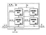
【0028】
異なる時点で、または異なる装置速度に対して、異なる終端回路が必要な場合、または装置10が異なる外部装置と接続している場合、図5のシステムが有用である。例えば、装置が33.3MHzで動作する時に回路14をイネーブルとし、一方装置10が50MHzで動作する時に回路50をイネーブルとする等というようなこともできる。回路52は、装置が低速のSRAMと交信している時にイネーブルとされ、一方終端回路54は、高速DRAM素子と交信している時にイネーブルとされる。他の場合では、2つ以上の回路14,50,52,54を同時にイネーブルとし、複数の終端素子または回路を、並列または直列に、或いは並列と直列との組み合わせで、結合することもできる。バス13、双方向バス、およびデータ・バスは、1ビットまたは1ビットより多いビット長とすることができる。これらが1ビットより長い場合、図1にあるように、バスの各ビットに対して回路500が複数個用いられる。
【0029】
例えば、図6は、4つの終端回路14,50,52,54を含む回路500を示す。図5のバス13、データバスおよび4本のイネーブル・ラインが図示されている。4本のイネーブル・ラインは、回路500内部で分割され、別々に名称を付けられ、イネーブル信号1〜4となる。各終端回路は、オン/オフ・スイッチとして機能する素子(即ち、バイポーラ・トランジスタ、MOSトランジスタ、JFET、SCR、トライアック(triac)、リレー等)と、バスのインピーダンスを変化させるすなわち信号反射を低減するように機能する素子を有していなければならない。切り替えおよび反射低減機能は、図6の回路/素子内の1つのトランジスタのような、単一素子によって実現することができる。
【0030】
終端回路14は、双方向バスとVddとの間に結合された終端回路/素子と、双方向バスと接地との間に結合された終端回路/素子510とを有する。終端回路50は、双方向バスとVddとの間に結合された終端回路/素子504と、双方向バスと接地との間に結合された終端回路/素子514とを有する。終端回路54は、双方向バスとVddとの間に結合された終端回路/素子508と、双方向バスと接地との間に結合された終端回路/素子516とを有する。
【0031】
イネーブル1がアクティブで他の全てのイネーブルがインアクティブの場合、回路/素子502,510のみが双方向バスに結合される。イネーブル1,2がアクティブで他の全てのイネーブルがインアクティブの場合、回路素子502が回路素子504と並列となり、回路/素子510が回路素子512と並列となって、異なる終端装置を形成する。
【0032】
例えば、一例として、回路/素子502が100オームの抵抗器およびスイッチであり、回路/素子504が50オームの抵抗器およびスイッチであり、回路/素子506が10オームの抵抗器およびスイッチであり、回路/素子508が3オームの抵抗器およびスイッチであるとする。これらのスイッチがイネーブル信号に結合されていれば、4つのイネーブルを16(24)の異なる状態を指定することができる。これら16通りの異なる状態において、100,50,10,3,33.33,8.33,2.91,7.69,2.75,2.16,9.09,2.30,2.83,2.20,2.26オームまたは無限大を、図6の回路における、双方向バスからVdd線までのバスのインピーダンスとして、選択的に選ぶことができる。別の実施形態では、8つのイネーブル信号を図6に用いることができ、1つのイネーブル信号を、図6の各終端回路/素子に結合する。8つのイネーブルを用いると、2の8乗個の異なる値を得ることができる。
【0033】
図7は、回路/素子520,522,524,526の他の相互接続を示す。ここでも、図7の回路/素子は、図6の回路/素子と同様であり、オン/オフ・スイッチとして機能する少なくとも1つの素子と、信号反射低減装置がなければならない。或いは多数の装置が一緒にまたは別個に、スイッチ機能と反射低減機能を実行する。図7は、回路500の相互接続によって、直列回路および並列回路を形成可能であることを示すものである。4つのイネーブル信号が示されている。図7のイネーブル信号の種々の状態から、9つまでの異なる終端インピーダンス値が得られる。例えば、回路/素子520が5オームの抵抗器と直列スイッチであり、回路/素子522が10オームの抵抗器と直列スイッチであり、回路/素子524が20オームの抵抗器と直列スイッチであり、回路/素子526が50オームの抵抗器と直列スイッチであると仮定する。すると、60,55,20,30,25,53.333,23.333,24.286,19.286オームおよび無限大の終端インピーダンスを得ることができる。また、図7は、図1〜図7における終端回路は常に接地とVddとの双方に結合しなくてはいけない訳ではないことも示すものである。代わりに、終端回路/素子は、Vddまたは接地のいずれかのみと、接続/結合すればよい。
【0034】
図8は、目的である直列終端をバス13と直列に選択的に結合するのに用いることができる、回路500を示す。図8は、4つの終端回路/素子600,601,602,603を示しており、これらはそれぞれイネーブル1〜4によって動作可能にされる。図8に示すように、終端回路および素子はいくつでも(4つのみでなく)接続してもよいことに注意されたい。イネーブル1〜4は独立にまたは集団でアクティブにしてもよく、図8の4つの終端回路/素子に対して16種類の異なる終端の組み合わせが得られる。終端回路/素子の1つを、直接電気的に短絡させてもよい。
【0035】
以上具体的な実施例を参照しながら本発明を図示し説明したが、当業者には更に変更や改善が思いつくであろう。例えば、バスに接続された2つ以上の装置、2つ以上のマスタ、および/または2つ以上状態を、図1〜図2のバスに結合してもよい。アドレス・バス、データ・バス、直列通信線、または制御信号のいずれかを、ここに教示した方法で終端することができる。信号反射を低減する終端回路または素子のいずれを用いてもよい。また、RCネットワークも、終端素子/回路として有用である。更に、データが実際にバス上を移動している短い時間だけ、終端素子をイネーブルにすることも有利である。更にまた、データ・バスのビット長は32ビットとしてもよく、この場合新たな転送によってバスの値が変わり(例えば16進値のFFFFFFFFから16進値のFFFFFFF7に)、32ビット値の内1つのビットのみが意味のある変化を行う。この場合、32個の終端回路の内1つの終端回路のみをイネーブルにして、反射を低減させればよい。バスに対して適正な終端値は、直列接続された抵抗である可能性がある(直列接続とは、受信ピンと入力バッファとの間で、バスと接続(in-line with)されることを意味する)ことに注意するのも重要である。図5の回路の構成は、リセット時に設定したり、外部から構成可能としたり、或いはユーザが構成可能とすることもできる。ここで例示したイネーブル以外のイネーブル制御信号も可能である。ここで教示された構造および方法は、双方向バスまたは単一方向バスの双方に用いることができる。したがって、本発明は例示された特定の形状に限定されるものではなく、本発明の真意および範囲から逸脱しない全ての変更を含むことを意図することは理解されよう。
【図面の簡単な説明】
【図1】本発明によるデータ処理システムのを示すロック図。
【図2】本発明による別のデータ処理システムを示すブロック図。
【図3】本発明による、集積回路の終端回路を動的にイネーブルする方法を示すフローチャート。
【図4】本発明による、集積回路の終端回路を動的にイネーブルする別の方法を示すフローチャート。
【図5】本発明による、データ処理システムの各外部入出力集積回路ピンに対する、複数の独立にイネーブルとされるバス終端回路を有するデータ処理システムを示すブロック図。
【図6】本発明による、図5の複数の独立してイネーブルとされるバス終端回路の相互接続を示すブロック図。
【図7】本発明による、図5の複数の独立してイネーブルとされるバス終端回路の別の相互接続を示すブロック図。
【図8】本発明による、図5の複数の独立してイネーブルとされるバス終端回路の更に別の相互接続を示すブロック図。
【符号の説明】
10,12 装置
13 双方向バス
14,16 動的バス終端回路
15,17 バス
18,20 データ部
22,24,26,28,34,36 トライステート・バッファ
30,32 排他的NOR(XNOR)ゲート[0001]
[Industrial application fields]
The present invention relates generally to data processing devices, and more particularly to a dynamic terminal of a conductive bus line that avoids signal reflection.
[0002]
[Background Art and Problems to be Solved by the Invention]
Devices that operate at high speeds, devices that operate at high clock frequencies, and / or devices that require very long conductive interconnects struggle with a performance-degrading phenomenon called signal reflection or transmission line effect problems This is well known in the art. This phenomenon is known and well understood. For example, if a 0 volt signal changes to a 5 volt signal on a long conductor or bus, or a conductor or bus operating at a high speed edge rate, the bus or conductor will have an appropriate impedance. If not terminated, it takes time to settle from 0 volts to 5 volts on that bus or conductor due to one or more reflections occurring at one or both terminals of the bus. In the past, in order to reduce signal reflection and thus improve performance, permanent resistors were placed at both ends of the one-way bus to reduce signal reflection. In this bus, one end always receives data (the other end always sends out). Termination of this one-way bus can be easily performed because termination is only required at the receiving side. However, when the bus is idle or partially in a low power mode of operation, the connected permanent resistor is usually disadvantageous, causing it to increase power consumption.
[0003]
In a bidirectional bus, the termination problem becomes even more serious because either end of the bus is receiving or transmitting at any time. Therefore, in the prior art, permanent resistance terminations are arranged and connected at both ends of the bus regardless of whether or not they are necessary. For this reason, when the bus is set to the low power operation mode, the load on the bus increases and the power consumption increases.
[0004]
The present invention seeks to overcome the aforementioned disadvantages and to obtain other advantages.
[0005]
[Means for Solving the Problems]
In one aspect, the present invention includes a method for determining whether to enable a termination circuit in a data processing device. Bus transfer begins through a bus coupled between the data processing device and an external device of the data processing device. It is determined whether the data processing device is receiving or sending data from outside the processing device. When the data processor is receiving data from the bus, enabling the termination circuit reduces signal reflection on the bus. When the data processing device is sending data through the bus, the termination circuit is disabled.
[0006]
In another aspect, the present invention includes a data processing system having a communication device, the communication device having at least one external pin connected to the outside thereof. The at least one external pin is coupled to receive data from outside the communication device and to transmit data outside the communication device. The communication device has a termination circuit. The termination circuit has a first input / output terminal coupled to the at least one external pin through at least one data line. The termination circuit has a second input / output terminal for supplying or receiving data from the inside to the communication device. The termination circuit has an input for receiving an enable signal and has one or more termination elements. The enable signal couples a termination element to the at least one termination pin when the enable signal is applied, and disconnects the termination element from the at least one termination pin when the enable signal is not applied.
[0007]
The invention will be more clearly understood from the following detailed description taken in conjunction with the accompanying drawings.
[0008]
【Example】
Embodiments of the present invention will be described below with reference to the drawings. In the drawings, it will be appreciated that for simplicity and clarity of illustration, elements depicted in the drawings are not necessarily drawn to scale. For example, the dimensions of certain elements are clearly expressed by exaggerating them compared to other elements. Further, where considered appropriate, reference numerals have been used repeatedly among the drawings to indicate corresponding or analogous elements.
[0009]
In general, the devices and methods illustrated herein are designed to dynamically enable proper termination in a receiver at the end of a bidirectional bus. By dynamically connecting the appropriate terminals to the bus only during data reception, signal reflection (ie transmission line effects) on the bus is reduced and higher operating speeds are possible. This dynamic bus termination requires a control signal that indicates to the receiving device the current bus drive direction (ie whether data is being read from or written to the device). When this control signal indicates that the voltage and / or current on the bus is being driven towards the receiving device, the receiving device switches on its terminating device and attenuates incoming signals. Therefore, the reflection is not returned to the bus (transmission line). Also, when the control signal indicates that the bus is not being driven toward the receiving device, the terminator of the receiving device is switched off, the load on the bus and the bus power. Reduce disappearance.
[0010]
An example of an apparatus that uses this dynamic termination method is an ultra-high speed processing apparatus that communicates through a bidirectional bus such as a data bus. In this case, the control signal that switches on the terminating network of the receiving processor will be a read / write (R / W *) line. It is advantageous to give the receiving devices time to enable their end networks using control lines that indicate the direction of the bus prior to the point at which the data is actually transferred. Note that the termination enable signal may be formed here using other bus termination control signals (other termination control signals are signals other than R / W * lines or master / slave * control signals). I want to be.
[0011]
The R / W * line is connected to the first bus line by the processing unit or when the processing unit is the bus owner (ie when the processing unit has mastership or ownership of the bus). Driven by the master. The R / W * signal indicates the direction of subsequent data transfer (ie, indicates whether data enters the first master (read) or data comes from the first master (write)). The R / W * signal goes high during a read bus cycle and goes low during a write bus cycle. When the first master is not a bus master, the R / W * signal is tristated. A signal containing “*” in the name means that it becomes active in some way when it is low. When the R / W * line is tri-stated by
[0012]
The preferred method and apparatus shown and taught herein solves the problem of providing proper termination for bidirectional transmission lines. In the known technology, it is necessary to terminate the bus at each end of the bus or at an intermediate point on the bus, or the bus must be configured in a star layout and the termination network must be centered on this star. is there. The use of static termination at either end or midpoint of the bus results in various known performance penalties. Performance can be improved if the end network can be dynamically switched to connect to or disconnected from the transmission line network and the proper end can be placed at the end of the bus, i.e., the final receiver, as required.
[0013]
Specifically, the apparatus and method shown here provide the capability to dynamically terminate a bi-directional bus according to the current bus drive direction. The method allows a termination network to be provided if necessary at the end of the net so that the transmission line can be properly terminated as if it were a unidirectional bus. This termination method only reduces the power consumed by the termination network of the system because only the termination network at the end of the bus needs to be enabled. In the case of a device that drives a high-speed bidirectional bus, it is necessary to properly provide a termination at the end point of a net that is normally input to another device to prevent signal reflection problems. However, if another device on the bi-directional bus drives the signal, the proper place for termination would be a different point on the net, either at the other end or usually another input device. Depending on the drive characteristics of the various device drivers on the bus, different termination methods / termination circuits or element values (eg, different resistors) are required to provide proper termination for the transmission line.
[0014]
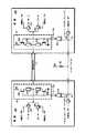
The present invention can be better understood with reference to FIGS. FIG. 1 shows a data processing system. The data processing system includes a
[0015]
[0016]
The termination circuit includes one or more circuit elements to reduce reflection when coupled to the data line, or to change the line impedance on the bidirectional
[0017]
Circuit components in
[0018]
[0019]
The operation of dynamic termination is described in further detail below. Assume that
[0020]
Assuming read access assuming the same control as described above,
[0021]
The advantage of using this mechanism is that the termination resistors can be dynamically enabled and provided at the receiver at the end of the bus to properly and reliably terminate the bi-directional transmission line. In addition, it is important to note that the present invention reduces power loss and bus line load by disabling or removing the termination network when the device is not receiving data. is there. This termination method only requires that the termination network at the end of the bus be operational at any point in time, thus reducing the power consumed by the termination network of the system. If the bus is not used at all, neither
[0022]
FIG. 2 shows a data processing system similar to FIG. 1 and the
[0023]
Since
[0024]
For example, each of the
[0025]
As described above,
[0026]
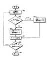
FIG. 3 illustrates a method used to dynamically terminate an integrated circuit. In
[0027]
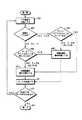
FIG. 4 shows another way of performing dynamic termination. Overall, FIG. 4 is similar to FIG. Step 400 is similar to step 300 of FIG. Step 402 is used to determine whether the device is a master device (ie, has ownership of the bus used for information communication).
[0028]
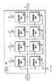
The system of FIG. 5 is useful when different termination circuits are required at different times or for different device speeds, or when the
[0029]
For example, FIG. 6 shows a
[0030]
[0031]
When enable 1 is active and all other enables are inactive, only circuits /
[0032]
For example, by way of example, circuit /
[0033]
FIG. 7 shows another interconnection of circuits /
[0034]
FIG. 8 shows a
[0035]
While the invention has been illustrated and described with reference to specific embodiments, further modifications and improvements will occur to those skilled in the art. For example, two or more devices connected to the bus, two or more masters, and / or two or more states may be coupled to the bus of FIGS. Either the address bus, data bus, serial communication line, or control signal can be terminated in the manner taught herein. Any termination circuit or element that reduces signal reflection may be used. An RC network is also useful as a termination element / circuit. It is also advantageous to enable the termination element only for a short period of time when data is actually moving on the bus. Furthermore, the bit length of the data bus may be 32 bits. In this case, the bus value is changed by a new transfer (for example, from FFFFFFFF of hexadecimal value to FFFFFFF7 of hexadecimal value), and one of the 32-bit values is changed. Only bits make meaningful changes. In this case, only one of the 32 termination circuits may be enabled to reduce reflection. A proper termination value for the bus may be a resistor connected in series (series connection means in-line with the bus between the receive pin and the input buffer) It is also important to note that. The configuration of the circuit in FIG. 5 can be set at the time of resetting, can be configured from the outside, or can be configured by the user. Enable control signals other than the enable exemplified here are also possible. The structures and methods taught herein can be used for both bidirectional or unidirectional buses. Thus, it will be understood that the invention is not limited to the specific shapes illustrated, but is intended to include all modifications that do not depart from the spirit and scope of the invention.
[Brief description of the drawings]
FIG. 1 is a lock diagram illustrating a data processing system according to the present invention.
FIG. 2 is a block diagram illustrating another data processing system according to the present invention.
FIG. 3 is a flowchart illustrating a method for dynamically enabling a termination circuit of an integrated circuit according to the present invention.
FIG. 4 is a flowchart illustrating another method of dynamically enabling termination circuits of an integrated circuit according to the present invention.
FIG. 5 is a block diagram illustrating a data processing system having a plurality of independently enabled bus termination circuits for each external input / output integrated circuit pin of the data processing system according to the present invention.
6 is a block diagram illustrating the interconnection of a plurality of independently enabled bus termination circuits of FIG. 5 in accordance with the present invention.
7 is a block diagram illustrating another interconnection of the plurality of independently enabled bus termination circuits of FIG. 5, in accordance with the present invention.
8 is a block diagram illustrating yet another interconnection of the plurality of independently enabled bus termination circuits of FIG. 5, in accordance with the present invention.
[Explanation of symbols]
10,12 equipment
13 Bidirectional bus
14,16 Dynamic bus termination circuit
15, 17 bus
18, 20 Data part
22, 24, 26, 28, 34, 36 Tristate buffer
30, 32 Exclusive NOR (XNOR) gate
Claims (4)
Translated fromJapanese前記複数の端子におけるデータ受信時の信号反射を低減するために必要なインピーダンスを決定する段階、
前記集積回路が読み出しまたは書き込み動作に付されていることを示す少なくとも1つの読み出し/書き込み信号からなる少なくとも1つの制御信号を前記複数の端子に結合された回路に通信する段階、そして
前記複数の端子がバスからデータを受信している時に前記複数の端子における信号反射を低減するために前記少なくとも1つの制御信号に基づく前記回路の出力により前記複数の端子の各々に、複数の可能なインピーダンスの内の1つのインピーダンスを選択して提供する段階、
を具備することを特徴とする方法。A method of providing selected impedances to a plurality of terminals of an integrated circuit used to communicate data in both directions, comprising:
Determining impedancerequired to reduce signal reflection during data reception at the plurality of terminals;
Communicating at least one control signal comprising at least one read / write signal indicating that the integrated circuit is undergoing a read or write operation to a circuit coupled to the plurality of terminals; and
A plurality of possible at each of the plurality of terminals by the output of the circuit based on the at least one control signal to reduce signal reflection at the plurality of terminals when the plurality of terminals are receiving data from the bus Selecting and providing one of the different impedances;
A method comprising the steps of:
前記データ処理装置内部の実行ユニット、
外部バスを通じて前記データ処理装置との間で論理ビットを双方向に通信するのに用いられる複数の外部ピン、
前記実行ユニットにデータを提供しあるいは前記実行ユニットからデータを受信する複数のバス終端回路であって、前記複数の外部ピンの各々に1つのバス終端回路が結合されており、前記複数のバス終端回路の各々は制御信号を受ける入力を有し、前記外部ピンが前記外部バスによってデータを送信している場合にディスエーブルされかつ前記外部ピンが前記外部バスからデータを受信している場合にイネーブルされるもの、そして
前記複数のバス終端回路の各々の入力に結合された導体は制御信号を提供し、該制御信号は前記複数のバス終端回路の各々に前記外部バスにおける信号反射を選択的に低減させるもの、
を具備することを特徴とするデータ処理装置。A data processing device,
An execution unit inside the data processing device,
A plurality of external pins used to bi-directionally communicate logic bits to and from the data processing device through an external bus;
A plurality of bus termination circuits for providing data to the execution unit or receiving data from the execution unit, wherein one bus termination circuit is coupled to each of the plurality of external pins; Each of the circuits has an input for receiving a control signal and is disabled when the external pin is transmitting data over the external bus and enabled when the external pin is receiving data from the external bus those are, andcoupled conductors to the inputs ofeach of said plurality of bus termination circuitprovides a control signal, said control signal selectively a signal reflection at the external busto each of the plurality of bus termination circuits To reduce
A data processing apparatus comprising:
前記データ処理装置と前記データ処理装置外部の装置との間で結合されたバスを介してバス転送を開始する段階、
前記データ処理装置が前記バスを介してデータを送信しているかあるいはデータを受信しているかを判定する段階、
前記データ処理装置が前記バスからデータを受信している場合に前記バス終端回路をイネーブルして前記バス上の信号反射を低減する段階、そして
前記データ処理装置が前記バスを介してデータを送信している場合に前記バス終端回路をディスエーブルする段階、
を具備することを特徴とする方法。A method for determining whether a termination circuit in a data processing device should be enabled by control logic in the data processing device, comprising:
Initiating a bus transfer via a bus coupled between the data processing device and a device external to the data processing device;
Determining whether the data processing device is transmitting data or receiving datavia the bus ;
Enabling thebus termination circuit to reduce signal reflection on thebus when the data processing device is receiving data from the bus; and the data processing device transmits data over the bus. Disabling thebus termination circuit if
A method comprising the steps of:
前記データ処理装置内部の実行ユニット、
外部バスを通じて前記データ処理装置との間で論理ビットを双方向に通信するのに用いられる複数の外部ピン、
前記実行ユニットにデータを提供しあるいは前記実行ユニットからデータを受信する複数のバス終端回路であって、前記複数の外部ピンの各々に1つのバス終端回路が結合されており、前記複数のバス終端回路の各々は制御信号を受けるための入力、対応する外部ピンに結合されたプルアップ装置、および前記対応する外部ピンに結合されたプルダウン装置を有するもの、そして
前記複数のバス終端回路の各々の入力に結合された導体は制御信号を提供し、該制御信号は、少なくとも部分的に、読み出し/書き込み信号に基づくものでありかつ前記複数のバス終端回路の各々に前記データ処理装置が前記外部バスからデータを受信している場合に前記外部バスにおける信号反射を選択的に低減させるもの、
を具備することを特徴とする相補金属酸化物半導体(CMOS)集積回路データ処理装置。A complementary metal oxide semiconductor (CMOS) integrated circuit data processing device comprising:
An execution unit inside the data processing device,
A plurality of external pins used to bi-directionally communicate logic bits to and from the data processing device through an external bus;
A plurality of bus termination circuits for providing data to the execution unit or receiving data from the execution unit, wherein one bus termination circuit is coupled to each of the plurality of external pins; input foreach circuit for receiving a control signal, corresponding pull-up device coupled to an external pin that, and those having a corresponding pull-down device coupled to the external pins, andeach of said plurality of bus termination circuits s Aconductor coupled to an input of the plurality of terminals provides a control signal, the control signal based at least in part on a read / write signal, and the data processing unit is connected to the external ofeach of the plurality of bus termination circuits Selectively reducing signal reflections on the external bus when receiving data from the bus;
Complementary metal oxide semiconductor (CMOS) integrated circuit data processing apparatus.
Applications Claiming Priority (2)
| Application Number | Priority Date | Filing Date | Title |
|---|---|---|---|
| US145117 | 1993-11-03 | ||
| US08/145,117US5467455A (en) | 1993-11-03 | 1993-11-03 | Data processing system and method for performing dynamic bus termination |
Publications (2)
| Publication Number | Publication Date |
|---|---|
| JPH07182078A JPH07182078A (en) | 1995-07-21 |
| JP4230545B2true JP4230545B2 (en) | 2009-02-25 |
Family
ID=22511674
Family Applications (1)
| Application Number | Title | Priority Date | Filing Date |
|---|---|---|---|
| JP28720694AExpired - LifetimeJP4230545B2 (en) | 1993-11-03 | 1994-10-28 | Data processing system and operation method |
Country Status (2)
| Country | Link |
|---|---|
| US (1) | US5467455A (en) |
| JP (1) | JP4230545B2 (en) |
Families Citing this family (114)
| Publication number | Priority date | Publication date | Assignee | Title |
|---|---|---|---|---|
| US5919252A (en)* | 1991-07-29 | 1999-07-06 | Micron Electronics, Inc. | Process and apparatus for adaptive bus termination |
| US5596757A (en)* | 1995-02-16 | 1997-01-21 | Simple Technology, Inc. | System and method for selectively providing termination power to a SCSI bus terminator from a host device |
| US5783963A (en)* | 1996-02-29 | 1998-07-21 | Lexmark International, Inc. | ASIC with selectable output drivers |
| US8604828B1 (en)* | 1996-05-31 | 2013-12-10 | International Business Machines Corporation | Variable voltage CMOS off-chip driver and receiver circuits |
| US5726583A (en)* | 1996-07-19 | 1998-03-10 | Kaplinsky; Cecil H. | Programmable dynamic line-termination circuit |
| AU7367698A (en)* | 1997-05-07 | 1998-11-27 | California Micro Devices Corporation | Active termination circuit and method therefor |
| US6128685A (en)* | 1998-02-18 | 2000-10-03 | Micron Technology, Inc. | Method for terminating a processor bus |
| US6122695A (en)* | 1998-02-18 | 2000-09-19 | Micron Technology, Inc. | Device for terminating a processor bus |
| US6510503B2 (en) | 1998-07-27 | 2003-01-21 | Mosaid Technologies Incorporated | High bandwidth memory interface |
| US6347350B1 (en) | 1998-12-22 | 2002-02-12 | Intel Corporation | Driving the last inbound signal on a line in a bus with a termination |
| US6438636B2 (en) | 1998-12-23 | 2002-08-20 | Intel Corporation | Updating termination for a bus |
| US6738844B2 (en)* | 1998-12-23 | 2004-05-18 | Intel Corporation | Implementing termination with a default signal on a bus line |
| US6674304B1 (en) | 1999-02-26 | 2004-01-06 | Motorola Inc. | Output buffer circuit and method of operation |
| US6453374B1 (en)* | 1999-03-30 | 2002-09-17 | Rockwell Collins, Inc. | Data bus |
| EP1050824A3 (en)* | 1999-04-22 | 2004-01-28 | Matsushita Electric Industrial Co., Ltd. | Bidirectional signal transmission circuit and bus system |
| US7010629B1 (en)* | 1999-12-22 | 2006-03-07 | Intel Corporation | Apparatus and method for coupling to a memory module |
| US6421794B1 (en)* | 2000-03-09 | 2002-07-16 | John T. Chen | Method and apparatus for diagnosing memory using self-testing circuits |
| JP4569912B2 (en)* | 2000-03-10 | 2010-10-27 | エルピーダメモリ株式会社 | Memory system |
| US6912170B1 (en)* | 2000-03-14 | 2005-06-28 | Micron Technology, Inc. | Method and apparatus for permanent electrical removal of an integrated circuit output after packaging |
| US6715014B1 (en)* | 2000-05-25 | 2004-03-30 | Hewlett-Packard Development Company, L.P. | Module array |
| US6356106B1 (en) | 2000-09-12 | 2002-03-12 | Micron Technology, Inc. | Active termination in a multidrop memory system |
| US6687780B1 (en)* | 2000-11-02 | 2004-02-03 | Rambus Inc. | Expandable slave device system |
| US6711639B1 (en) | 2000-11-02 | 2004-03-23 | Dell Products L.P. | System and method for processor bus termination |
| US6510100B2 (en)* | 2000-12-04 | 2003-01-21 | International Business Machines Corporation | Synchronous memory modules and memory systems with selectable clock termination |
| JP2002197051A (en)* | 2000-12-11 | 2002-07-12 | Internatl Business Mach Corp <Ibm> | Method for selecting communication adapter for determining communication destination, method for setting communication adapter, computer device, portable information device, and storage medium |
| US6674648B2 (en)* | 2001-07-23 | 2004-01-06 | Intel Corporation | Termination cards and systems therefore |
| US6674649B2 (en) | 2001-07-23 | 2004-01-06 | Intel Corporation | Systems having modules sharing on module terminations |
| US6711027B2 (en)* | 2001-07-23 | 2004-03-23 | Intel Corporation | Modules having paths of different impedances |
| US6771515B2 (en)* | 2001-07-23 | 2004-08-03 | Intel Corporation | Systems having modules with on die terminations |
| US6631083B2 (en) | 2001-07-23 | 2003-10-07 | Intel Corporation | Systems with modules and clocking therefore |
| US6918078B2 (en)* | 2001-07-23 | 2005-07-12 | Intel Corporation | Systems with modules sharing terminations |
| JP3799251B2 (en)* | 2001-08-24 | 2006-07-19 | エルピーダメモリ株式会社 | Memory device and memory system |
| JP3821678B2 (en) | 2001-09-06 | 2006-09-13 | エルピーダメモリ株式会社 | Memory device |
| KR100468728B1 (en)* | 2002-04-19 | 2005-01-29 | 삼성전자주식회사 | On-chip terminator, Control circuit there-of and Control method there-of in semiconductor integrated circuit |
| JP2004021916A (en)* | 2002-06-20 | 2004-01-22 | Renesas Technology Corp | Data bus |
| DE10235158A1 (en)* | 2002-08-01 | 2004-02-19 | Daimlerchrysler Ag | Characteristic wave impedance matching circuit arrangement has matching resistance network between chokes and vehicle data bus line ends for characteristic wave impedance matching of data bus lines |
| US7142461B2 (en)* | 2002-11-20 | 2006-11-28 | Micron Technology, Inc. | Active termination control though on module register |
| US20040177204A1 (en)* | 2003-01-30 | 2004-09-09 | Campbell David C. | Bus interface with variable resistance coupling |
| US6838907B1 (en)* | 2003-02-27 | 2005-01-04 | Marvell Semiconductor Israel Ltd. | Supplying logic values for sampling on high-speed interfaces |
| US6937058B2 (en)* | 2003-07-16 | 2005-08-30 | Infineon Technologies Ag | Methods and apparatus for active termination of high-frequency signals |
| US6924660B2 (en)* | 2003-09-08 | 2005-08-02 | Rambus Inc. | Calibration methods and circuits for optimized on-die termination |
| US6980020B2 (en)* | 2003-12-19 | 2005-12-27 | Rambus Inc. | Calibration methods and circuits for optimized on-die termination |
| US7788451B2 (en) | 2004-02-05 | 2010-08-31 | Micron Technology, Inc. | Apparatus and method for data bypass for a bi-directional data bus in a hub-based memory sub-system |
| US7257683B2 (en) | 2004-03-24 | 2007-08-14 | Micron Technology, Inc. | Memory arbitration system and method having an arbitration packet protocol |
| US7196567B2 (en)* | 2004-12-20 | 2007-03-27 | Rambus Inc. | Systems and methods for controlling termination resistance values for a plurality of communication channels |
| US9542352B2 (en) | 2006-02-09 | 2017-01-10 | Google Inc. | System and method for reducing command scheduling constraints of memory circuits |
| US8244971B2 (en) | 2006-07-31 | 2012-08-14 | Google Inc. | Memory circuit system and method |
| US20080082763A1 (en) | 2006-10-02 | 2008-04-03 | Metaram, Inc. | Apparatus and method for power management of memory circuits by a system or component thereof |
| US9171585B2 (en) | 2005-06-24 | 2015-10-27 | Google Inc. | Configurable memory circuit system and method |
| US8090897B2 (en) | 2006-07-31 | 2012-01-03 | Google Inc. | System and method for simulating an aspect of a memory circuit |
| US8041881B2 (en) | 2006-07-31 | 2011-10-18 | Google Inc. | Memory device with emulated characteristics |
| US9507739B2 (en) | 2005-06-24 | 2016-11-29 | Google Inc. | Configurable memory circuit system and method |
| US8077535B2 (en) | 2006-07-31 | 2011-12-13 | Google Inc. | Memory refresh apparatus and method |
| US7580312B2 (en) | 2006-07-31 | 2009-08-25 | Metaram, Inc. | Power saving system and method for use with a plurality of memory circuits |
| US8060774B2 (en) | 2005-06-24 | 2011-11-15 | Google Inc. | Memory systems and memory modules |
| US7392338B2 (en) | 2006-07-31 | 2008-06-24 | Metaram, Inc. | Interface circuit system and method for autonomously performing power management operations in conjunction with a plurality of memory circuits |
| US8386722B1 (en) | 2008-06-23 | 2013-02-26 | Google Inc. | Stacked DIMM memory interface |
| US7609567B2 (en) | 2005-06-24 | 2009-10-27 | Metaram, Inc. | System and method for simulating an aspect of a memory circuit |
| US8055833B2 (en) | 2006-10-05 | 2011-11-08 | Google Inc. | System and method for increasing capacity, performance, and flexibility of flash storage |
| US20080028136A1 (en) | 2006-07-31 | 2008-01-31 | Schakel Keith R | Method and apparatus for refresh management of memory modules |
| US8796830B1 (en) | 2006-09-01 | 2014-08-05 | Google Inc. | Stackable low-profile lead frame package |
| US7386656B2 (en) | 2006-07-31 | 2008-06-10 | Metaram, Inc. | Interface circuit system and method for performing power management operations in conjunction with only a portion of a memory circuit |
| US8327104B2 (en) | 2006-07-31 | 2012-12-04 | Google Inc. | Adjusting the timing of signals associated with a memory system |
| KR101377305B1 (en) | 2005-06-24 | 2014-03-25 | 구글 인코포레이티드 | An integrated memory core and memory interface circuit |
| US8130560B1 (en) | 2006-11-13 | 2012-03-06 | Google Inc. | Multi-rank partial width memory modules |
| US8089795B2 (en) | 2006-02-09 | 2012-01-03 | Google Inc. | Memory module with memory stack and interface with enhanced capabilities |
| US8359187B2 (en) | 2005-06-24 | 2013-01-22 | Google Inc. | Simulating a different number of memory circuit devices |
| US8335894B1 (en) | 2008-07-25 | 2012-12-18 | Google Inc. | Configurable memory system with interface circuit |
| US7590796B2 (en) | 2006-07-31 | 2009-09-15 | Metaram, Inc. | System and method for power management in memory systems |
| US8081474B1 (en) | 2007-12-18 | 2011-12-20 | Google Inc. | Embossed heat spreader |
| US8438328B2 (en) | 2008-02-21 | 2013-05-07 | Google Inc. | Emulation of abstracted DIMMs using abstracted DRAMs |
| US8111566B1 (en) | 2007-11-16 | 2012-02-07 | Google, Inc. | Optimal channel design for memory devices for providing a high-speed memory interface |
| US8397013B1 (en) | 2006-10-05 | 2013-03-12 | Google Inc. | Hybrid memory module |
| US10013371B2 (en) | 2005-06-24 | 2018-07-03 | Google Llc | Configurable memory circuit system and method |
| WO2007028109A2 (en) | 2005-09-02 | 2007-03-08 | Metaram, Inc. | Methods and apparatus of stacking drams |
| US7372293B2 (en)* | 2005-12-07 | 2008-05-13 | Intel Corporation | Polarity driven dynamic on-die termination |
| US7439760B2 (en)* | 2005-12-19 | 2008-10-21 | Rambus Inc. | Configurable on-die termination |
| US9632929B2 (en) | 2006-02-09 | 2017-04-25 | Google Inc. | Translating an address associated with a command communicated between a system and memory circuits |
| US7486104B2 (en) | 2006-06-02 | 2009-02-03 | Rambus Inc. | Integrated circuit with graduated on-die termination |
| US7724589B2 (en) | 2006-07-31 | 2010-05-25 | Google Inc. | System and method for delaying a signal communicated from a system to at least one of a plurality of memory circuits |
| US7417464B2 (en)* | 2006-09-22 | 2008-08-26 | Integrated Electronic Solutions Pty. Ltd | Bi-directional signal transmission system |
| WO2008079911A1 (en) | 2006-12-21 | 2008-07-03 | Rambus Inc. | Dynamic on-die termination of address and command signals |
| US7595657B2 (en)* | 2007-05-01 | 2009-09-29 | Sony Corporation | Dynamic dual control on-die termination |
| US8209479B2 (en) | 2007-07-18 | 2012-06-26 | Google Inc. | Memory circuit system and method |
| US8080874B1 (en) | 2007-09-14 | 2011-12-20 | Google Inc. | Providing additional space between an integrated circuit and a circuit board for positioning a component therebetween |
| JP2009237678A (en)* | 2008-03-26 | 2009-10-15 | Fujitsu Microelectronics Ltd | Memory controller device, control method for memory controller device and data reception device |
| US8041865B2 (en)* | 2008-08-04 | 2011-10-18 | Qimonda Ag | Bus termination system and method |
| JP2010170296A (en) | 2009-01-22 | 2010-08-05 | Elpida Memory Inc | Memory system, semiconductor memory device, and wiring substrate |
| US7843225B2 (en)* | 2009-04-14 | 2010-11-30 | Via Technologies, Inc. | Protocol-based bus termination for multi-core processors |
| US8085062B2 (en)* | 2009-04-14 | 2011-12-27 | Via Technologies, Inc. | Configurable bus termination for multi-core/multi-package processor configurations |
| US8242802B2 (en)* | 2009-04-14 | 2012-08-14 | Via Technologies, Inc. | Location-based bus termination for multi-core processors |
| DE202010017690U1 (en) | 2009-06-09 | 2012-05-29 | Google, Inc. | Programming dimming terminating resistor values |
| JP5346259B2 (en) | 2009-09-08 | 2013-11-20 | ルネサスエレクトロニクス株式会社 | Semiconductor integrated circuit |
| JP5390310B2 (en) | 2009-09-08 | 2014-01-15 | ルネサスエレクトロニクス株式会社 | Semiconductor integrated circuit |
| JP5363252B2 (en) | 2009-09-09 | 2013-12-11 | ルネサスエレクトロニクス株式会社 | Semiconductor integrated circuit |
| KR101789077B1 (en)* | 2010-02-23 | 2017-11-20 | 삼성전자주식회사 | On-die termination circuit, data output buffer, semiconductor memory device, memory module, method of operating an on-die termination circuit, method of operating a data output buffer and method of training on-die termination |
| CN102859598A (en) | 2010-06-17 | 2013-01-02 | 拉姆伯斯公司 | Balanced on-die termination |
| US8018250B1 (en)* | 2010-10-19 | 2011-09-13 | Xilinx, Inc. | Input/output block and operation thereof |
| KR101796116B1 (en) | 2010-10-20 | 2017-11-10 | 삼성전자 주식회사 | Semiconductor device, memory module and memory system having the same and operating method thereof |
| US8637212B2 (en) | 2010-12-22 | 2014-01-28 | Via Technologies, Inc. | Reticle set modification to produce multi-core dies |
| US9460038B2 (en)* | 2010-12-22 | 2016-10-04 | Via Technologies, Inc. | Multi-core microprocessor internal bypass bus |
| US8930676B2 (en) | 2010-12-22 | 2015-01-06 | Via Technologies, Inc. | Master core discovering enabled cores in microprocessor comprising plural multi-core dies |
| US8972707B2 (en) | 2010-12-22 | 2015-03-03 | Via Technologies, Inc. | Multi-core processor with core selectively disabled by kill instruction of system software and resettable only via external pin |
| US8631256B2 (en) | 2010-12-22 | 2014-01-14 | Via Technologies, Inc. | Distributed management of a shared power source to a multi-core microprocessor |
| US8782451B2 (en) | 2010-12-22 | 2014-07-15 | Via Technologies, Inc. | Power state synchronization in a multi-core processor |
| KR101273241B1 (en)* | 2011-08-19 | 2013-06-11 | 포항공과대학교 산학협력단 | A low-power high-speed data transceiver |
| US8937490B2 (en)* | 2011-10-24 | 2015-01-20 | Samsung Electronics Co., Ltd. | Output driver, devices having the same, and ground termination |
| KR20130045144A (en)* | 2011-10-24 | 2013-05-03 | 삼성전자주식회사 | Output driver, devices having the same, and ground termination |
| EP2813074B1 (en)* | 2012-02-06 | 2018-02-21 | Nishil Thomas Koshy | Variable impedance scheme for providing high speed wired communication |
| US9088445B2 (en) | 2013-03-07 | 2015-07-21 | Qualcomm Incorporated | Method and apparatus for selectively terminating signals on a bidirectional bus based on bus speed |
| JP5612185B2 (en)* | 2013-10-10 | 2014-10-22 | ルネサスエレクトロニクス株式会社 | Semiconductor integrated circuit |
| DE102018203671A1 (en) | 2018-03-12 | 2019-09-12 | Robert Bosch Gmbh | Transceiver for a bus system and method for reducing conducted emissions |
| KR102649322B1 (en) | 2018-05-25 | 2024-03-20 | 삼성전자주식회사 | Memory device, memory system, and oepration method of memory device |
| US10812075B2 (en)* | 2019-05-20 | 2020-10-20 | Intel Corporation | Dynamic on-die termination |
Family Cites Families (16)
| Publication number | Priority date | Publication date | Assignee | Title |
|---|---|---|---|---|
| US3435375A (en)* | 1965-09-20 | 1969-03-25 | Motorola Inc | Controller having fet bridge circuit |
| US3854057A (en)* | 1972-12-11 | 1974-12-10 | Lrc Corp | High speed impedance sensitive switch driver |
| US4567385A (en)* | 1983-06-22 | 1986-01-28 | Harris Corporation | Power switched logic gates |
| US4695740A (en)* | 1984-09-26 | 1987-09-22 | Xilinx, Inc. | Bidirectional buffer amplifier |
| EP0258808B1 (en)* | 1986-08-29 | 1993-02-24 | Mitsubishi Denki Kabushiki Kaisha | Complementary mos integrated circuit |
| US4839537A (en)* | 1986-11-29 | 1989-06-13 | Kabushiki Kaisha Toshiba | BicMO logic circuit |
| JPH0728214B2 (en)* | 1987-02-06 | 1995-03-29 | 株式会社日立製作所 | Semiconductor integrated circuit device |
| US4761647A (en)* | 1987-04-06 | 1988-08-02 | Intel Corporation | Eprom controlled tri-port transceiver |
| US4791322A (en)* | 1987-05-19 | 1988-12-13 | Gazelle Microcircuits, Inc. | TTL compatible input buffer |
| US4877978A (en)* | 1988-09-19 | 1989-10-31 | Cypress Semiconductor | Output buffer tri-state noise reduction circuit |
| JPH02132917A (en)* | 1988-11-14 | 1990-05-22 | Toshiba Corp | bus driver integrated circuit |
| US5063308A (en)* | 1988-12-21 | 1991-11-05 | Intel Corporation | Output driver with static and transient parts |
| US4975598A (en)* | 1988-12-21 | 1990-12-04 | Intel Corporation | Temperature, voltage, and process compensated output driver |
| US5057783A (en)* | 1990-02-16 | 1991-10-15 | Beckman Industrial Corporation | Automatic impedance matching |
| US5039874A (en)* | 1990-03-15 | 1991-08-13 | Hewlett-Packard Company | Method and apparatus for driving an integrated-circuit output pad |
| US5162672A (en)* | 1990-12-24 | 1992-11-10 | Motorola, Inc. | Data processor having an output terminal with selectable output impedances |
- 1993
- 1993-11-03USUS08/145,117patent/US5467455A/ennot_activeExpired - Lifetime
- 1994
- 1994-10-28JPJP28720694Apatent/JP4230545B2/ennot_activeExpired - Lifetime
Also Published As
| Publication number | Publication date |
|---|---|
| US5467455A (en) | 1995-11-14 |
| JPH07182078A (en) | 1995-07-21 |
Similar Documents
| Publication | Publication Date | Title |
|---|---|---|
| JP4230545B2 (en) | Data processing system and operation method | |
| US5528168A (en) | Power saving terminated bus | |
| US5111080A (en) | Complementary signal transmission circuit with impedance matching circuitry | |
| US6054881A (en) | Input/output (I/O) buffer selectively providing resistive termination for a transmission line coupled thereto | |
| KR100437233B1 (en) | Integrated circuit chip with adaptive input-output port | |
| US5859541A (en) | Data processor having an output terminal with selectable output impedances | |
| KR100431651B1 (en) | On-chip termination | |
| US5781028A (en) | System and method for a switched data bus termination | |
| US6611552B2 (en) | Universal serial bus transceiver and associated methods | |
| US5311081A (en) | Data bus using open drain drivers and differential receivers together with distributed termination impedances | |
| US5264744A (en) | Complementary signal transmission circuit with impedance matching circuitry | |
| US20100064083A1 (en) | Communications device without passive pullup components | |
| JPH06224731A (en) | Control impedance transistor switching circuit | |
| JPH01501275A (en) | Terminator for transceiver | |
| US6222389B1 (en) | Assisted gunning transceiver logic (AGTL) bus driver | |
| US6218854B1 (en) | Data line termination circuits and integrated circuit devices including attenuation circuit and charge/discharge circuit | |
| US6738844B2 (en) | Implementing termination with a default signal on a bus line | |
| US6232814B1 (en) | Method and apparatus for controlling impedance on an input-output node of an integrated circuit | |
| US6735657B1 (en) | Method and apparatus for connecting two-wire serial interface and single-wire serial interface with high transmission speed | |
| KR20030024890A (en) | Method and apparatus for combining architectures with logic option | |
| CA1241084A (en) | Bidirectional bus arrangement for a digital communication system | |
| US6239619B1 (en) | Method and apparatus for dynamic termination logic of data buses | |
| JPH03116214A (en) | Terminating circuit | |
| JP3008873B2 (en) | Signal transmission equipment | |
| US6335632B1 (en) | CMOS small signal switchable terminator network |
Legal Events
| Date | Code | Title | Description |
|---|---|---|---|
| A977 | Report on retrieval | Free format text:JAPANESE INTERMEDIATE CODE: A971007 Effective date:20041021 | |
| A131 | Notification of reasons for refusal | Free format text:JAPANESE INTERMEDIATE CODE: A131 Effective date:20041102 | |
| A521 | Request for written amendment filed | Free format text:JAPANESE INTERMEDIATE CODE: A523 Effective date:20050201 | |
| RD02 | Notification of acceptance of power of attorney | Free format text:JAPANESE INTERMEDIATE CODE: A7422 Effective date:20050201 | |
| A711 | Notification of change in applicant | Free format text:JAPANESE INTERMEDIATE CODE: A711 Effective date:20041217 | |
| A02 | Decision of refusal | Free format text:JAPANESE INTERMEDIATE CODE: A02 Effective date:20050510 | |
| A521 | Request for written amendment filed | Free format text:JAPANESE INTERMEDIATE CODE: A523 Effective date:20050907 | |
| A911 | Transfer to examiner for re-examination before appeal (zenchi) | Free format text:JAPANESE INTERMEDIATE CODE: A911 Effective date:20051024 | |
| A912 | Re-examination (zenchi) completed and case transferred to appeal board | Free format text:JAPANESE INTERMEDIATE CODE: A912 Effective date:20060120 | |
| A601 | Written request for extension of time | Free format text:JAPANESE INTERMEDIATE CODE: A601 Effective date:20080611 | |
| A602 | Written permission of extension of time | Free format text:JAPANESE INTERMEDIATE CODE: A602 Effective date:20080616 | |
| A601 | Written request for extension of time | Free format text:JAPANESE INTERMEDIATE CODE: A601 Effective date:20080711 | |
| A602 | Written permission of extension of time | Free format text:JAPANESE INTERMEDIATE CODE: A602 Effective date:20080717 | |
| A601 | Written request for extension of time | Free format text:JAPANESE INTERMEDIATE CODE: A601 Effective date:20080807 | |
| A602 | Written permission of extension of time | Free format text:JAPANESE INTERMEDIATE CODE: A602 Effective date:20080812 | |
| A521 | Request for written amendment filed | Free format text:JAPANESE INTERMEDIATE CODE: A523 Effective date:20080911 | |
| RD04 | Notification of resignation of power of attorney | Free format text:JAPANESE INTERMEDIATE CODE: A7424 Effective date:20081111 | |
| RD03 | Notification of appointment of power of attorney | Free format text:JAPANESE INTERMEDIATE CODE: A7423 Effective date:20081114 | |
| A01 | Written decision to grant a patent or to grant a registration (utility model) | Free format text:JAPANESE INTERMEDIATE CODE: A01 | |
| A61 | First payment of annual fees (during grant procedure) | Free format text:JAPANESE INTERMEDIATE CODE: A61 Effective date:20081204 | |
| R150 | Certificate of patent or registration of utility model | Free format text:JAPANESE INTERMEDIATE CODE: R150 | |
| FPAY | Renewal fee payment (event date is renewal date of database) | Free format text:PAYMENT UNTIL: 20111212 Year of fee payment:3 | |
| FPAY | Renewal fee payment (event date is renewal date of database) | Free format text:PAYMENT UNTIL: 20111212 Year of fee payment:3 | |
| FPAY | Renewal fee payment (event date is renewal date of database) | Free format text:PAYMENT UNTIL: 20121212 Year of fee payment:4 | |
| FPAY | Renewal fee payment (event date is renewal date of database) | Free format text:PAYMENT UNTIL: 20131212 Year of fee payment:5 | |
| R250 | Receipt of annual fees | Free format text:JAPANESE INTERMEDIATE CODE: R250 | |
| EXPY | Cancellation because of completion of term |