JP4227892B2 - Cold cathode tube driving device and liquid crystal display device - Google Patents
Cold cathode tube driving device and liquid crystal display deviceDownload PDFInfo
- Publication number
- JP4227892B2 JP4227892B2JP2003509616AJP2003509616AJP4227892B2JP 4227892 B2JP4227892 B2JP 4227892B2JP 2003509616 AJP2003509616 AJP 2003509616AJP 2003509616 AJP2003509616 AJP 2003509616AJP 4227892 B2JP4227892 B2JP 4227892B2
- Authority
- JP
- Japan
- Prior art keywords
- pulse
- dispersion
- frequency
- pulse width
- output
- Prior art date
- Legal status (The legal status is an assumption and is not a legal conclusion. Google has not performed a legal analysis and makes no representation as to the accuracy of the status listed.)
- Expired - Fee Related
Links
Images


Classifications
- H—ELECTRICITY
- H05—ELECTRIC TECHNIQUES NOT OTHERWISE PROVIDED FOR
- H05B—ELECTRIC HEATING; ELECTRIC LIGHT SOURCES NOT OTHERWISE PROVIDED FOR; CIRCUIT ARRANGEMENTS FOR ELECTRIC LIGHT SOURCES, IN GENERAL
- H05B41/00—Circuit arrangements or apparatus for igniting or operating discharge lamps
- H05B41/14—Circuit arrangements
- H05B41/36—Controlling
- H05B41/38—Controlling the intensity of light
- H05B41/39—Controlling the intensity of light continuously
- H05B41/392—Controlling the intensity of light continuously using semiconductor devices, e.g. thyristor
- H05B41/3921—Controlling the intensity of light continuously using semiconductor devices, e.g. thyristor with possibility of light intensity variations
- H05B41/3925—Controlling the intensity of light continuously using semiconductor devices, e.g. thyristor with possibility of light intensity variations by frequency variation
- H—ELECTRICITY
- H05—ELECTRIC TECHNIQUES NOT OTHERWISE PROVIDED FOR
- H05B—ELECTRIC HEATING; ELECTRIC LIGHT SOURCES NOT OTHERWISE PROVIDED FOR; CIRCUIT ARRANGEMENTS FOR ELECTRIC LIGHT SOURCES, IN GENERAL
- H05B41/00—Circuit arrangements or apparatus for igniting or operating discharge lamps
- H05B41/14—Circuit arrangements
- H05B41/26—Circuit arrangements in which the lamp is fed by power derived from DC by means of a converter, e.g. by high-voltage DC
- H05B41/28—Circuit arrangements in which the lamp is fed by power derived from DC by means of a converter, e.g. by high-voltage DC using static converters
- H05B41/282—Circuit arrangements in which the lamp is fed by power derived from DC by means of a converter, e.g. by high-voltage DC using static converters with semiconductor devices
- H05B41/2821—Circuit arrangements in which the lamp is fed by power derived from DC by means of a converter, e.g. by high-voltage DC using static converters with semiconductor devices by means of a single-switch converter or a parallel push-pull converter in the final stage
- H05B41/2822—Circuit arrangements in which the lamp is fed by power derived from DC by means of a converter, e.g. by high-voltage DC using static converters with semiconductor devices by means of a single-switch converter or a parallel push-pull converter in the final stage using specially adapted components in the load circuit, e.g. feed-back transformers, piezoelectric transformers; using specially adapted load circuit configurations
- H—ELECTRICITY
- H05—ELECTRIC TECHNIQUES NOT OTHERWISE PROVIDED FOR
- H05B—ELECTRIC HEATING; ELECTRIC LIGHT SOURCES NOT OTHERWISE PROVIDED FOR; CIRCUIT ARRANGEMENTS FOR ELECTRIC LIGHT SOURCES, IN GENERAL
- H05B41/00—Circuit arrangements or apparatus for igniting or operating discharge lamps
- H05B41/14—Circuit arrangements
- H05B41/26—Circuit arrangements in which the lamp is fed by power derived from DC by means of a converter, e.g. by high-voltage DC
- H05B41/28—Circuit arrangements in which the lamp is fed by power derived from DC by means of a converter, e.g. by high-voltage DC using static converters
- H05B41/282—Circuit arrangements in which the lamp is fed by power derived from DC by means of a converter, e.g. by high-voltage DC using static converters with semiconductor devices
- H05B41/2821—Circuit arrangements in which the lamp is fed by power derived from DC by means of a converter, e.g. by high-voltage DC using static converters with semiconductor devices by means of a single-switch converter or a parallel push-pull converter in the final stage
- H05B41/2824—Circuit arrangements in which the lamp is fed by power derived from DC by means of a converter, e.g. by high-voltage DC using static converters with semiconductor devices by means of a single-switch converter or a parallel push-pull converter in the final stage using control circuits for the switching element
- H—ELECTRICITY
- H05—ELECTRIC TECHNIQUES NOT OTHERWISE PROVIDED FOR
- H05B—ELECTRIC HEATING; ELECTRIC LIGHT SOURCES NOT OTHERWISE PROVIDED FOR; CIRCUIT ARRANGEMENTS FOR ELECTRIC LIGHT SOURCES, IN GENERAL
- H05B41/00—Circuit arrangements or apparatus for igniting or operating discharge lamps
- H05B41/14—Circuit arrangements
- H05B41/36—Controlling
- H05B41/38—Controlling the intensity of light
- H05B41/39—Controlling the intensity of light continuously
- H05B41/392—Controlling the intensity of light continuously using semiconductor devices, e.g. thyristor
- H05B41/3921—Controlling the intensity of light continuously using semiconductor devices, e.g. thyristor with possibility of light intensity variations
- H05B41/3927—Controlling the intensity of light continuously using semiconductor devices, e.g. thyristor with possibility of light intensity variations by pulse width modulation
- Y—GENERAL TAGGING OF NEW TECHNOLOGICAL DEVELOPMENTS; GENERAL TAGGING OF CROSS-SECTIONAL TECHNOLOGIES SPANNING OVER SEVERAL SECTIONS OF THE IPC; TECHNICAL SUBJECTS COVERED BY FORMER USPC CROSS-REFERENCE ART COLLECTIONS [XRACs] AND DIGESTS
- Y02—TECHNOLOGIES OR APPLICATIONS FOR MITIGATION OR ADAPTATION AGAINST CLIMATE CHANGE
- Y02B—CLIMATE CHANGE MITIGATION TECHNOLOGIES RELATED TO BUILDINGS, e.g. HOUSING, HOUSE APPLIANCES OR RELATED END-USER APPLICATIONS
- Y02B20/00—Energy efficient lighting technologies, e.g. halogen lamps or gas discharge lamps
Landscapes
- Engineering & Computer Science (AREA)
- Power Engineering (AREA)
- Discharge-Lamp Control Circuits And Pulse- Feed Circuits (AREA)
- Circuit Arrangements For Discharge Lamps (AREA)
- Dc-Dc Converters (AREA)
Description
Translated fromJapanese【0001】
【発明の属する技術分野】
本発明は、例えば液晶パネルのバックライトである冷陰極管を駆動するための昇圧トランスとして圧電トランスが用いられる冷陰極管駆動装置、およびその冷陰極管駆動装置を搭載した液晶表示装置に関する。
【0002】
【従来の技術】
液晶パネルのバックライトである冷陰極管を駆動するための昇圧トランスとして、電磁トランスに代わって、薄型化、高効率化が可能な圧電トランスが用いられるようになってきた。圧電トランスは、圧電素子のピエゾ効果を利用して機械振動を発生させ、二次側電極から圧電トランスの形状で定まる昇圧比で電圧増幅された電圧を取り出す電圧変換素子である。
【0003】
圧電トランスの一般的な特性を図40に示す。圧電トランスは共振特性を持つため、一次側に入力される交流電圧の周波数に応じて、二次側の出力電圧が変化する。このような特性から、バックライトの輝度を一定に制御するため方法としては、次の形態が一般的である。すなわち、圧電トランスを駆動する交流電圧の周波数を制御して、二次側電圧の振幅が所望のレベルになるようにし、冷陰極管に安定した電圧を印加する方法である。制御に当っては、共振周波数より高い周波数領域のリニアな傾斜部分を利用する。
【0004】
図41はバックライト駆動部の一般的な構成を示す。図41において、1は圧電トランス、2はコイル、3はスイッチングトランジスタ(FET(電界効果トランジスタ))、4は冷陰極管、5は冷陰極管4に流れる電流を検出する電流検出器、6は電流検出器5による検出電圧と基準電圧を比較して、その差に応じた周波数の駆動パルスを生成する駆動パルス生成回路である。
【0005】
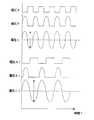
図42は図41に示す回路の各部の波形を示す。図42において、電圧Aは駆動パルス生成回路6の出力電圧波形(駆動パルス)、電圧Bは圧電トランス1の入力電圧波形、電圧Cは圧電トランス1の出力電圧波形で、この電圧Cが冷陰極管4に与えられて、冷陰極管4に電流(管電流)が流れ、電流検出器5で検出される。圧電トランス1の入力電圧は、正弦波電圧が望ましいが、ここでは半波の正弦波電圧で説明する。
【0006】
コイル2と圧電トランス1は共振回路を構成しており、その共振周波数はコイル2のインダクタンス値と圧電トランス1の入力容量値で決まる。この共振回路にFET3を介してエネルギーを与えることにより、前記共振周波数で半波の正弦波波形が得られる(電圧B)。電圧Bが入力された圧電トランス1の出力からは、圧電トランス1自体の持つ共振周波数成分のみが抜き出され、図42の電圧Cの正弦波電圧が出力される。この正弦波電圧Cは、図40に示す特性から電圧Bの周波数によってその振幅が変化する。
【0007】
駆動パルス生成回路6では、この特性を利用し、電流検出器5から得られる電圧と基準電圧を比較し、管電流が所望の値になるように駆動パルス生成回路6の出力電圧の周波数を制御する。図42の電圧A1〜C1に駆動パルスの周波数を低くした場合の各部波形を示す。周波数が低くなるに従って正弦波電圧の振幅が大きくなる。
【0008】
このように圧電トランス1の駆動回路においては、冷陰極管4の輝度を制御するに当たり、駆動パルスの周波数を変えることにより管電流を制御する方法が一般的に用いられる。
【0009】
上記の技術を実現する回路は、従来、アナログで構成されるのが一般的であった。このため、部品点数が多く、かつ部品スペースも大きいという課題があった。特に、カメラ一体型VTRやディジタルカメラなどの携帯用映像機器では機器の小型化が重要なため、駆動回路の省スペース化が望まれていた。
【0010】
これを鑑み、駆動回路をディジタル化し、他のLSI(例えば液晶コントローラ等)と1チップ化することによって駆動回路のスペースを削減し、かつコスト削減を行う試みがなされている(例えば、特許文献1参照)。
【0011】
ディジタル方式での圧電トランスの駆動で実用的な調光分解能を得るためには、通常、数100MHz〜数GHzのクロックを必要とする。特許文献1の技術は、駆動パルスの周波数を分散させる方式で10MHz程度のクロックで、周波数制御による調光分解能を可能にする。
【0012】
この特許文献1に示された技術を簡単に説明する。ディジタルで駆動パルスを生成する場合、クロックを単純に分周して駆動パルスを得る方法では調光に必要な周波数分解能が得られない。圧電トランスの共振の鋭さQは非常に大きく、例えば圧電トランスの駆動周波数を約100KHzとした場合、調光に必要な周波数分解能は、100KHz近辺で数10Hz刻みの分解能が必要となる。ところが、例えばクロック周波数が10MHzで、このクロックを用いて100KHzの駆動パルスを生成する場合、100KHz近辺で約1KHz程度の周波数分解能しか得られず、調光性能のみならず安定点灯すら実現が困難である。
【0013】
そこで、図43に示すように、所定の駆動周期内で分周比を分散させ、平均の周波数で分解能を得るように構成される。この方法により、例えば100周期の中で分周比を分散させれば、100倍の周波数分解能を得ることができる。この方法により、冷陰極管駆動装置をディジタルLSIに内蔵することが可能となり、省スペース化、低コスト化が可能となる。
【0014】
上記特許文献1に示す駆動方法は、管電流を制御して調光を行う方式である。しかしながら、管電流の制御で調光を行う方法では、
(1)管電流が小さい領域では、冷陰極管に流れる電流が安定しないため、調光レベルをあまり小さくできない。
【0015】
(2)冷陰極管の発光効率は電流値によって変化し、管電流制御では調光レベルに応じて効率が大きく変化する。
【0016】
(3)管電流を変えるには駆動周波数を変える必要があるが、圧電トランスの効率は駆動周波数によって変化するため、広い調光範囲で高効率を得るには限界がある。
【0017】
これらの課題を解決する手段として、輝度フリッカとならない周波数(例えば100Hz程度)で間欠的に駆動をON・OFFして調光する手法(以下バースト調光と記す)が知られており、このON・OFFのデューティ比率を変えることにより調光レベルを変えるものがある。この方法は、圧電トランスを用いたバックライト駆動回路のみならず、従来の電磁トランスを用いたバックライト駆動回路でも広く用いられている。
【0018】
圧電トランスを用いたバックライト駆動回路で、このバースト調光を実現する方式は、大きくは次の2つがある。1つは回路電源をON・OFFさせる方法、もう1つは回路を動作させておいて駆動パルスのみON・OFFする方法である。
【0019】
前者については、従来回路でも対応が可能で、電源ON時の始動制御と点灯時の通常制御を繰り返すだけであるが、電源をON・OFFするために電源ラインに遮断回路が必要であり、この遮断回路によって電力ロスが発生するため、特に携帯用の機器では好ましくない。
【0020】
一方、後者については、従来回路に加え、駆動OFF時に管電流の検出をOFFし、駆動周波数を所定の値に保持する手段が必要である。この場合、電源ラインでのロスがなく、特に携帯用機器用途では優れた方式である。これをアナログ方式で実現する技術については、例えば特許文献2に示されている。
【0021】
特許文献2に示されている方式を簡単に説明する。図44は特許文献2に示されている方法を簡略化した図で、特徴とするところは、サンプルホールド手段8により、駆動OFF時に電流検出器5の電圧を保持し、これによって、電圧制御発振回路12の発振周波数を一定レベルに保持し、駆動再開時に速やかに点灯を開始するようにしている。
【0022】
【特許文献1】
特開2000−133485号公報
【特許文献2】
特開平11-298060号公報
【特許文献3】
特開平8−33349号公報
【特許文献4】
特開2000−139081号公報
【0023】
【発明が解決しようとする課題】
上述したように、アナログ駆動方式では、バースト調光駆動方式については、簡単な回路の追加で、実現可能である。しかしながら、バースト調光を周波数分散方式によるディジタル方式で実現する場合、以下の課題がある。
【0024】
(1)周波数分散方式は、所定の周期で駆動パルスの周波数を分散させ平均周波数で周波数分解能を得る仕組みであり、分散周期を1セットとして電流制御を行うため、ON・OFFのデューティ比率を任意に変えた場合、分散方式の原理上正しい電流検出が行えず、電流制御が著しく不安定になる。
【0025】
(2)図45に示すように分散原理を崩さず、分散周期単位でデューティ比率を変える場合、必要な調光分解能を得るためには、調光分解能に応じた分散周期セットが必要になり、これにより、バースト周期の周波数が著しく低くなり、輝度フリッカが大となる。また、バースト周期を輝度フリッカが抑えられるレベルまで高くした場合、調光分解能が得られない。
【0026】
さらには、アナログ・ディジタル共通の課題として、バースト調光時(特に目標の輝度レベルが小さい場合)の始動制御の課題がある。本来点灯時は、所望の輝度で点灯することが望ましい。しかしながら、従来の駆動回路では以下に説明する理由でこれが困難であった。
【0027】
所望の輝度で点灯させる方法は次の2つがある。第1の方法は、図46に示すように、始動時も点灯時と同じくバースト駆動で行う方法である。この方法は、始動時も点灯時と同じバースト制御となるため、余分な回路を必要としない。また、点灯時に目標の輝度レベルに違和感なく移行するため、良好な点灯品位を得ることができる。
【0028】
しかしながら、この方法では、特に目標の輝度レベルが低い場合、冷陰極管の点灯性が低くなる。
【0029】
一般に冷陰極管は低温時や、周囲照度が暗い場合、点灯性能が低くなる。この問題は、始動電圧を高くしたり、始動電圧を印加する時間を長くしたりすれば改善されることが知られている。
【0030】
しかしながら、バースト駆動による始動では、始動電圧を印加する時間が余分に必要であるため、点灯に時間がかかる。
【0031】
加えて、始動時に圧電トランスに高圧による余分なストレスがかかるのを防ぐため、所定時間経過しても点灯しない場合は始動を停止するという保護機能がある。この保護機能の影響で点灯に至らない場合も発生する。
【0032】
また、バースト駆動時の始動電圧を高くする方法があるが、圧電トランスにさらにストレスがかかり、信頼性が劣化する。また、高圧による放電防止対策の強化に余分な回路スペースが必要なため得策ではない。
【0033】
第2の方法は、図47に示すように始動時は冷陰極管の点灯性を鑑みて連続で駆動し、点灯後速やかにバースト駆動に移行する方法である。この方法は、始動時と点灯時で制御が異なるため、点灯検出手段と制御の切換手段が必要になるが、理想的な点灯検出手段を得ることができれば、冷陰極管の点灯性を低下させることなく、目標の輝度レベルで点灯が可能となる。
【0034】
しかしながら、従来の点灯検出手段では、点灯検出の遅れが大きく、図47に示すように、目標の輝度レベルに達するまでに輝度が大きく変化し、点灯品位の問題が発生する。
【0035】
本発明は、上記した課題を鑑みてなされたもので、第1に、ディジタル方式でバースト調光を実現する駆動方式を提案し、バースト調光可能な冷陰極管駆動装置の低コスト、省スペースを実現することを目的とする。
【0036】
また、第2に目標の輝度レベルが低い場合でも、点灯性の優れた始動方式を得ることを目的とする。
【0037】
本発明の他の目的、特徴、利点は、後述から明かになるであろう。
【0038】
【課題を解決するための手段】
〔第1の解決手段〕
上記の目的を達成するために、第1の解決手段として、第1の本発明(請求項1に対応)は、負荷である冷陰極管を駆動するための昇圧トランスとして、入力電圧の周波数に応じて出力電圧が変化する圧電トランスを用いる冷陰極管駆動装置であって、それぞれ次のような機能を有する構成要素「データ変換手段、平滑処理手段、誤差電圧演算手段、周波数設定手段、分周手段、制御コントローラ、バーストパルス発生手段、出力イネーブル手段および電力増幅手段」を含んでいる。これらの各手段は、ハードウエアで構成してもよいし、ソフトウエアで構成してもよいし、あるいはハードウエアとソフトウエアとのハイブリッド構成としてもよい。即ち、第1の本発明(請求項1に対応)は、入力電圧の周波数に応じて変化する出力電圧を負荷である冷陰極管に出力する圧電トランスと、前記冷陰極管に流れる電流を検出し、その電流量をディジタルデータに変換するデータ変換手段と、前記データ変換手段の出力データを所定のタイミングで平滑する平滑処理手段と、前記平滑処理手段から得られる平滑データと基準データとを比較し、その差分に相当する誤差データを出力する誤差電圧演算手段と、前記誤差データに基づいて前記駆動パルスの周波数を設定する周波数設定手段と、所定の周波数のクロックを分周して前記駆動パルスの分散数Nで決まるN周期期間(Nは自然数)である分散周期で前記周波数設定手段から出力される周波数データに対応した平均周波数の駆動パルスを発生させる分周手段と、予め決められた回数A(AはA≧2の自然数)だけ前記平均周波数で同一駆動を行うように制御周期をコントロールする制御コントローラと、バーストパルス発生手段と、外部から与えられる調光レベルに応じたデューティ幅のパルスでかつ前記制御コントローラから出力される周波数のパルスを発生させる制御コントローラと、前記バーストパルス発生手段の出力値に応じて、前記分周手段からの駆動パルスの出力をON・OFFする出力イネーブル手段と、前記出力イネーブル手段からの駆動パルスによるスイッチングで半波の正弦波電圧に変換(インバータ変換)した上で前記圧電トランスに出力する前記電力増幅手段とを含む冷陰極管駆動装置である。なお、前記駆動パルスのN周期期間を“分散周期”と呼ぶこともできる。以上の構成により、調光レベルを制御して冷陰極管の輝度レベルを調整する。なお、この構成については後述する実施の形態1での図2を参照することができる。
【0039】
この構成による作用は次のとおりである。制御周期を分散周期(駆動パルスN周期分)のA倍とし、同一の平均周波数でA回駆動するように構成して、バーストパルスのアクティブ期間の幅が分散周期より短くならないように設定している。
【0040】
分周手段は、分周比の組み合わせによる平均周波数をもつ分散周期での駆動を制御周期にわたってA回繰り返すことにより、高精度の周波数分解能を得る。これに対応して、負荷である冷陰極管に流れる電流の検出も分散周期単位とするのが原則となる。しかし、管電流が一定になるようにバースト駆動の制御を1分散周期単位で行うと、バーストパルス幅(ON期間)が分散周期より短くなり、ON時の電流を一定に制御することができなくなる。このため、バーストパルス幅(ON期間)は1分散周期より短くならないように、そして、電流検出のサンプル数が分散周期期間のサンプル数と等しくなるように、同一の平均周波数で複数回駆動(分散周期複数回)する。このように構成することにより、確実に1分散周期中の平均電流を検出する期間を確保する。その結果、管電流一定の制御を良好に行うことができる。
【0041】
換言すれば、制御周期を分散周期のA倍(自然数)とし、同一の平均周波数でA回駆動することにより、駆動パルスの周波数分散によるディジタル駆動方式においても、良好なバースト調光を実現することができる。具体的には次のとおりである。ディジタル駆動方式であるので、駆動回路のスペースの削減と低コスト化とを実現できる。また、周波数分散方式であるので、良好な調光性能、点灯性能に必要な周波数分解能が得られる。また、バースト調光方式であるので、管電流制御方式に見られるような輝度フリッカを抑制することができる。また、駆動パルスのON・OFF方式であるので、電源ON・OFF方式に見られるような電力ロスがなく、遮断回路も不要である。そして、上記のとおり、特に、制御周期を分散周期のA倍とし、同一の平均周波数でA回駆動する方式のバースト調光を行うので、高い調光分解能を確保しながら、管電流一定制御による輝度フリッカ防止を実現することができる。
【0042】
第2の本発明(請求項2に対応)は、前記平滑処理手段は、前記バーストパルス発生手段が生成するバーストパルスのパルス幅に応じて、その平滑するデータの取得範囲が前記分散数Nで決まるN周期の整数倍単位で可変されるようにしたことを特徴とする第1の発明に記載の冷陰極管駆動装置である。なお、これについては、後述する実施の形態1の図7および図8を参照することができる。より具体的レベルでは、前記バーストパルス発生手段からのバーストパルスと前記制御コントローラからの制御タイミングパルスに基づいて前記データの取得範囲を演算する検出幅調整手段を設けることである。このようにバーストパルス幅に応じてデータ取得範囲を調整することにより、調光レベルが大きくなるほど電流検出精度が向上する。
【0043】
また、上記において好ましい態様は、前記平滑処理手段が平均処理を行うもの(平均処理手段)として構成されていることである。負荷である冷陰極管に流れる電流を高精度に検出するためには平均処理手段を用いることが好ましい。ただし、特に厳密な輝度精度を必要としない場合には、通常のフィルタ手段に置き換えてもよい。
【0044】
上記第1の解決手段において、前記平滑処理手段、前記誤差電圧演算手段、前記周波数設定手段、前記分周手段、前記制御コントローラ、前記バーストパルス発生手段および前記出力イネーブル手段からなる制御処理手段については、これをハードウエアで構成することのほか、ソフトウエアで構成してもよし、あるいはそれらのハイブリッド構成でもよい。なお、ソフトウエアで構成する場合については後述する実施の形態1の変形の態様の図20を参照することができる。
【0045】
そして、上記の構成の冷陰極管駆動装置を搭載した液晶表示装置は、上記した各課題を解決している。その構成は、液晶パネルと、前記液晶パネルのバックライトである冷陰極管と、上記構成の冷陰極管駆動装置とを含み、前記冷陰極管駆動装置における前記圧電トランスが前記冷陰極管に接続された構成である。上記構成の冷陰極管駆動装置における出力イネーブル手段からの駆動パルスを電力増幅手段におけるスイッチング素子に供給して圧電トランスを駆動し、調光レベルを制御して液晶パネルに表示する画像の輝度レベルを調整する。
【0046】
この発明によれば、液晶パネルのバックライトである冷陰極管を圧電トランスで駆動する方式の液晶表示装置において、駆動パルスの周波数分散によるディジタル駆動で圧電トランスを駆動するにつけて、バースト調光を実現することができる。すなわち、所要の調光に必要な周波数分解能が得られるため、管電流が比較的小さい領域でも冷陰極管に流れる電流が安定し、調光レベルを小さくすることができる。そして、ディジタル駆動方式の副次的な効果として、他のLSIとの1チップ化による低コスト化および省スペース化が図られ、小型映像機器の小型化に貢献することができる。
【0047】
〔第2の解決手段〕
第2の解決手段として、本発明は、負荷である冷陰極管を駆動するための昇圧トランスとして、入力電圧の周波数に応じて出力電圧が変化する圧電トランスを用いる冷陰極管駆動装置であって、第1の解決手段と同様に構成されたデータ変換手段、平滑処理手段、誤差電圧演算手段、周波数設定手段、分周手段、制御コントローラ、バーストパルス発生手段、出力イネーブル手段および電力増幅手段を含んでいることに加えて、前記制御コントローラは、予め決められた回数A×k(A≧2、kは前記分散周期に応じて変動する値)だけ前記平均周波数で同一駆動を行うように制御周期をコントロールするように構成され、さらに、新たな構成要素として次のような機能を分散数調整手段を含んでいる。すなわち、前記分散数調整手段は、前記バーストパルス発生手段から出力されるバーストパルス幅に連動して前記分散周期を決める前記Nおよびkの値を設定する。以上の構成により、調光レベルを制御して冷陰極管の輝度レベルを調整する。即ち、第3の本発明(請求項3に対応)は、前記冷陰極管駆動装置は、更に分散数調整手段を有し、前記分散数調整手段は、前記バーストパルス発生手段から出力されるバーストパルス幅と、前記分散数Nと、前記予め決められた回数Aと、前記分散数Nに応じて変動する値kとに基づいて、前記制御周期の値A×N×kが所定の値になるように調整し、前記コントローラは、前記予め決められた回数Aと前記分散数Nに応じて変動する値kとの積で決まる回数A×k回だけ前記平均周波数で同一駆動を行うように制御周期をコントロールすることを特徴とする第1〜2の発明のいずれかに記載の冷陰極管駆動装置である。
【0048】
上記第1の解決手段と比較して第2の解決手段の特徴は、制御コントローラの構成が異なることと、分散数調整手段が追加されている点である。この分散数調整手段は、ハードウエア、ソフトウエアのいずれでもかまわないし、あるいはそれらのハイブリッド構成でもよい。前記制御コントローラについて、第1の解決手段では与えられた所定の回数A(A≧2)だけ同一の平均周波数で繰り返し駆動を行うように制御周期をコントロールする。これに対して、第2の解決手段では、kを分散周期に応じて変動する値として、与えられた所定の回数A×kだけ同一の平均周波数で繰り返し駆動を行うように制御周期をコントロールする。加えて、バーストパルス幅に連動して分散周期を決める前記Nおよびkの値を設定するための分散数調整手段を追加している。なお、第2の解決手段の構成については後述する実施の形態2での図9を参照することができる。また、kの値を可変することについては、図10を参照することができる。
【0049】
上記第2の解決手段において好ましい態様は、前記分散数調整手段について、前記制御コントローラによる制御周期が前記N(分散周期を決める)の値に関わらず一定になるように、前記分散数調整手段が前記kの値を決めることである。即ち、第4の本発明(請求項4に対応)は、前記冷陰極管駆動装置は、更に分散数調整手段を有し、前記分散数調整手段は、前記バーストパルス発生手段から出力されるバーストパルス幅と、前記分散数Nと、前記予め決められた回数Aとに応じて変動する値kとに基づいて、前記制御周期の値A×N×kが一定になるように調整するようにしたことを特徴とする第1〜2の発明のいずれかに記載の冷陰極管駆動装置である。
【0050】
また、上記第2の解決手段において好ましい態様においては、第5の本発明(請求項5に対応)は、前記分散数調整手段は、前記バーストパルス発生手段から出力されるバーストパルスのデューティに連動して、前記制御コントローラの前記Aの値を調整するようにしたことを特徴とする第1〜2発明のいずれかに記載の冷陰極管駆動装置である。
【0051】
上記構成による作用は次のとおりである。負荷である冷陰極管に流れる平均電流を正しく検出するには、最低1分散周期の検出範囲が必要である。上記の第1の解決手段1では、バーストパルス幅を分散周期幅より大きくする必要があり、調光レベルの下限に制約がある。これに鑑みたのが第2の解決手段である。すなわち、バーストパルス幅に応じて、分散数N(分散周期)を変えるが、分散周期が変わっても制御周期(つまりバーストパルスの周期)が変わらないように、同一の平均周波数で駆動する回数を同時に変える。端的には、N×kを一定にする。
【0052】
1分散周期期間の検出を確保するのに、分散数が多いとバーストパルスのデューティも大きく、分散数が少ないとデューティも小さくてよい。一方、電流精度は分散数が多い方が高い。しかし、調光精度を必要とするのは、通常、映像鑑賞として使用される約50〜100%の調光レベルであり、低輝度部では、高輝度部ほど調光精度を必要としない。低輝度モードは待機モードやOSD(オンスクリーンディスプレイ)のみしか表示しないときに消費電力を削減するために使用される。そこで、低輝度の場合(バーストパルスの幅が所定以下になった場合)は、分散数を小さくして、かつバースト周波数が変わらないように、同一周波数で駆動する回数を多くする(図10参照)。そこで、バーストパルス幅に応じて分散数を変えることにより、調光レベルを小さくすることが可能となり、調光範囲の拡大が可能になる。
【0053】
さらに好ましい態様は、前記平滑処理手段について、前記バーストパルス発生手段が生成するバーストパルスのパルス幅に応じて、平滑するデータの取得範囲が前記分散周期の整数倍単位で可変されるように平滑処理手段が構成されていることである。より具体的レベルでは、前記バーストパルス発生手段からのバーストパルスと前記制御コントローラからの制御タイミングパルスに基づいて前記データの取得範囲を演算する検出幅調整手段を設けることである(図7、図8参照)。このようにバーストパルス幅に応じてデータ取得範囲を調整することにより、調光レベルが大きくなるほど電流検出精度が向上する。
【0054】
また、上記において好ましい態様は、前記平滑処理手段が平均処理を行うもの(平均処理手段)として構成されていることである。負荷である冷陰極管に流れる電流を高精度に検出するためには平均処理手段を用いることが好ましい。ただし、特に厳密な輝度精度を必要としない場合には、通常のフィルタ手段に置き換えてもよい。
【0055】
上記第2の解決手段において、前記平滑処理手段、前記誤差電圧演算手段、前記周波数設定手段、前記分周手段、前記制御コントローラ、前記分散数調整手段、前記バーストパルス発生手段および前記出力イネーブル手段からなる制御処理手段については、これをハードウエアで構成することのほか、ソフトウエアで構成してもよし、あるいはそれらのハイブリッド構成でもよい。
【0056】
そして、上記の構成の冷陰極管駆動装置を搭載した液晶表示装置の構成は、液晶パネルと、前記液晶パネルのバックライトである冷陰極管と、上記構成の冷陰極管駆動装置とを含み、前記冷陰極管駆動装置における前記圧電トランスが前記冷陰極管に接続された構成である。上記構成の冷陰極管駆動装置における出力イネーブル手段からの駆動パルスを電力増幅手段におけるスイッチング素子に供給して圧電トランスを駆動し、調光レベルを制御して液晶パネルに表示する画像の輝度レベルを調整する。
【0057】
この発明によれば、液晶パネルのバックライトである冷陰極管を圧電トランスで駆動する方式の液晶表示装置において、第1の解決手段と同様に、駆動パルスの周波数分散によるディジタル駆動で圧電トランスを駆動するにつけて、バースト調光を実現することができる。すなわち、所要の調光に必要な周波数分解能が得られるため、管電流が比較的小さい領域でも冷陰極管に流れる電流が安定し、調光レベルを小さくすることができる。加えて、バーストパルス幅に応じて分散数を変えることにより、調光レベルをさらに小さくすることが可能となり、調光範囲を拡大することができる。
【0058】
〔第3の解決手段〕
第3の解決手段として、本発明は、負荷である冷陰極管を駆動するための昇圧トランスとして、入力電圧の周波数に応じて出力電圧が変化する圧電トランスを用いる冷陰極管駆動装置であって、第1の解決手段と同様に構成されたデータ変換手段、平滑処理手段、誤差電圧演算手段、周波数設定手段、分周手段、制御コントローラ、バーストパルス発生手段、出力イネーブル手段および電力増幅手段を含んでいることに加えて、前記データ変換手段は、前記冷陰極管に流れる電流および前記冷陰極管の入力電圧を検出し、それぞれの電気量をディジタルデータに変換する。さらに、新たな構成要素として次のような機能を有する点灯検出手段、制御周期切換手段および調光レベル切換手段を含んでいる。これらの各手段は、ハードウエアで構成してもよいし、ソフトウエアで構成してもよいし、あるいはハードウエアとソフトウエアとのハイブリッド構成としてもよい。
【0059】
第6の本発明(請求項6に対応)は、前記冷陰極管駆動装置は、更に、点灯検出手段と、制御周期切換手段と、調光レベル切換手段とを有し、前記点灯検出手段は前記データ変換手段の出力から点灯を検出して点灯検出パルスを出力し、前記制御周期切換手段は前記点灯検出手段から出力される点灯検出パルスに連動して前記回数Aの値を切り換え、前記調光レベル切換手段は前記点灯検出手段から出力される点灯検出パルスに連動して外部から与えられる調光レベルと別途設定された調光レベルとを切り換えることを特徴とする請求項1、3、4のいずれかに記載の冷陰極管駆動装置である。このようにして得た調光レベルを前記バーストパルス発生手段に与える。以上の構成により、調光レベルを制御して冷陰極管の輝度レベルを調整する。
【0060】
上記第1の解決手段と比較して第3の解決手段の特徴は、データ変換手段の構成が異なることと、新たな構成要素として点灯検出手段と制御周期切換手段と調光レベル切換手段が追加されている点である。データ変換手段については、冷陰極管に流れる電流の検出機能に加えて、冷陰極管の入力電圧を検出する機能を備えている。加えて、データ変換手段の出力から点灯を検出する点灯検出手段と、点灯検出手段から出力される点灯検出パルスに連動して前記回数Aの値を切り換える制御周期切換手段と、点灯検出パルスに連動して外部から与えられる調光レベルと別途設定された調光レベルとを切り換える調光レベル切換手段とを追加している。なお、前記制御コントローラについては、第1の解決手段と同様に、予め決められた回数A(Aは2以上の自然数)だけ前記平均周波数で同一駆動を行うように制御周期をコントロールする。なお、第3の解決手段の構成については後述する実施の形態3での図13を参照することができる(平滑処理手段については、その一例として平均処理手段とされている)。
【0061】
上記第3の解決手段において好ましい態様は、前記制御周期切換手段で設定される制御周期を示す回数Aの値について、点灯時に対し始動時の値の方が小さくなるように設定されていることである。
【0062】
また、第7の本発明(請求項7に対応)は、上記第3の解決手段において好ましい態様においては、前記分周手段の分散周期は、前記点灯検出手段から出力される点灯検出パルスに連動して切り換えられ、貫通点灯時の分散周期よりも始動時の分散周期の方が小さくなるように設定されていることを特徴とする請求項1、3、4、6のいずれかに記載の冷陰極管駆動装置である。
【0063】
また、第8の本発明(請求項8に対応)は、上記第3の解決手段において好ましい態様においては、前記調光レベル切換手段は、前記点灯検出手段から出力される点灯検出パルスが非点灯を示す値のときは100%連続駆動を示す調光レベルを出力するようにしたことを特徴とする請求項1、3、4、6のいずれかに記載の冷陰極管駆動装置である。
【0064】
上記構成による作用は次のとおりである。調光レベルとバーストパルス幅とは相関する。バーストパルスが有効のときに圧電トランスが駆動され、冷陰極管に電圧が印加される。調光レベルが低くバーストパルス幅が小さいと、始動時の点灯性能が悪くなる。これに鑑みたのが第3の解決手段である。始動時において、冷陰極管の点灯が実現するまでは、調光レベル切換手段において、高めの調光レベルとなるようにバーストパルス幅を大きめに設定する。例えば、調光レベルを100%として、連続駆動とする。これによると、圧電トランスから冷陰極管に対する電圧印加の時間を長く確保できる。また、制御周期切換手段において、制御周期を短めに設定する。これにより、MIN調光時のバーストパルス幅以内で点灯検出を行い、点灯直後の輝度の変動を抑える。点灯完了によって冷陰極管に管電流が流れると、これを点灯検出手段が検出し、制御周期切換手段および調光レベル切換手段を制御する。点灯検出後すみやかに所望の調光レベルに移行する。以上の相乗により、調光レベルが低い場合であっても、点灯性能が良好なものとなる。
【0065】
そして、点灯検出手段からの点灯検出パルスに基づいて分散数調整手段を制御し、始動時の分散数を貫通点灯時の分散数より小さくするようにすれば、点灯時の輝度変化であるイレギュラー期間を短くして、点灯品位を改善し、さらに良好な点灯性能が得られる。
【0066】
上記第3の解決手段において、前記平滑処理手段、前記誤差電圧演算手段、前記周波数設定手段、前記分周手段、前記制御コントローラ、前記制御周期切換手段、前記調光レベル切換手段、前記バーストパルス発生手段および前記出力イネーブル手段からなる制御処理手段については、これをハードウエアで構成することのほか、ソフトウエアで構成してもよいし、あるいはそれらのハイブリッド構成でもよい。
【0067】
そして、第9の本発明は、液晶パネルと、前記液晶パネルのバックライトである冷陰極管と、上記の第1〜8の本発明のいずれかに記載の冷陰極管駆動装置とを含み、前記冷陰極管駆動装置における前記圧電トランスが前記冷陰極管に接続されていることを特徴とする液晶表示装置である。この液晶表示装置によれば、液晶パネルのバックライトである冷陰極管の調光レベルが低い場合であっても、点灯性能が良好なものとなる。
【0068】
ところで、バックライトの冷陰極管を駆動させるための圧電トランスに求められるものは、基本的には、調光機能、低電力(高い電力変換効率)等である。さらには、ノートパソコンやディジタルビデオカメラなどの携帯機器に用いる場合、その電源はバッテリである。しかし、バッテリ電源では安定した電源が得られない。したがって、バッテリ電源に着目すると、広い電源電圧範囲で安定した点灯、安定した電力変換効率が望まれる。
【0069】
その対策として、アナログ駆動方式で電源電圧に応じて駆動のデューティ比を変えることが従来より提案されている。しかし、これをディジタル駆動方式で行う場合、クロック周波数が低いとデューティ比の分解能が粗く、十分な性能が得られない。クロック周波数を高くすれば分解能を確保できるが、回路電力の増加、輻射妨害の増加があり、実用的でなくなる。したがって、広い電源電圧範囲で良好な性能を求めるには、駆動パルスのデューティ比はできるだけ小刻みに調整できることが望ましい。
【0070】
以下に記述する第4以下の解決手段は、上記課題に鑑みたもので、ディジタル駆動方式で効率劣化のないデューティ制御方式を提案し、広い電源電圧範囲に対応する冷陰極管駆動装置を実現するものである。
【0071】
電源電圧変動を加味した冷陰極管駆動装置についての本発明は、次のような手段を講じることにより、上記の課題を解決する。
【0072】
〔第4の解決手段〕
第4の解決手段の本発明は、圧電トランスの負荷である冷陰極管における電気量と基準の電気量との差分に相当する分周比に応じて所定周波数のクロックを分周した駆動パルスを生成し、前記圧電トランスに出力する冷陰極管駆動装置において、次のような機能を有する構成要素〜周波数設定手段、分周手段、電源電圧検出手段、パルス幅演算手段およびパルス幅調整手段〜を含んでいる。これらの各手段は、ハードウエアで構成してもよいし、ソフトウエアで構成してもよいし、あるいはハードウエアとソフトウエアとのハイブリッド構成としてもよい。
【0073】
前記周波数設定手段は、前記差分の情報から前記駆動パルスについての分周比情報を求め、分周手段およびパルス幅演算手段に与えるものである。前記分周手段は、前記周波数設定手段による前記分周比情報に基づいて分周比を分散する状態のパルスである分散パルス(分周比分散駆動パルス)を生成するものである。前記電源電圧検出手段は、電源電圧を検出し、その電源電圧情報を前記パルス幅演算手段に与えるものである。前記パルス幅演算手段は、前記電源電圧検出手段からの電源電圧情報と前記周波数設定手段からの分周比情報とに基づいて分散パルスについてのパルス幅情報を演算し、前記パルス幅調整手段に与えるものである。前記パルス幅調整手段は、前記パルス幅演算手段からのパルス幅情報に基づいて前記分散パルスのパルス幅を拡張した拡張パルスを生成するとともに、前記パルス幅情報に基づいて前記分散パルスと前記拡張パルスとを切り換えて圧電トランスの駆動素子に対して出力するものである。なお、この構成については後述する実施の形態4での図21を参照することができる。
【0074】
この構成による作用は次のとおりである。パルス幅演算手段は、検出した電源電圧に応じたパルス幅情報をパルス幅調整手段に与える。原則として、電源電圧が低くなるほどパルス幅を大きくする(図24参照)。パルス幅調整手段は、分散パルスから拡張パルスを生成するとともに、パルス幅情報つまりは検出電源電圧に基づいて分散パルスと拡張パルスのいずれかを選択して、圧電トランスの駆動素子へ出力する。
【0075】
分散パルスから拡張パルスを生成することをディジタル的に行う。分散パルスのタイミングをずらせたパルスを生成し、このタイミングのずれたパルスと元の分散パルスとを論理和合成することにより、分散パルスよりもパルス幅の広い拡張パルスを生成することができる。前記のずらせたタイミングの時間幅だけ拡幅されている。どれだけずらせるかは、検出電源電圧に対応したパルス幅情報に基づいて決められる。また、元の分散パルスと拡張パルスのいずれを選択するかもパルス幅情報に基づいて決定される。このような処理により、検出電源電圧に対応したパルス幅の駆動パルスのディジタル的な生成が実現される。ずらせる時間幅をなるべく小さくする。
【0076】
これにより、ディジタル駆動方式においても広い電源電圧範囲で最適なパルス幅の駆動パルスが得られる。駆動パルスのパルス幅分解能を分散パルスの2倍にすることができる。これは、圧電トランスの駆動において、効率改善による消費電力削減を図るとともに、サージに起因する駆動素子(FET)や圧電トランスの破壊を防止することができ、その効果は大きい。
【0077】
なお、分散パルスからタイミングのずれたパルスを生成するには、クロックの立ち上がりエッジでラッチする方式、遅延素子を用いる方式、これら両方式を組み合わせた方式がある。
【0078】
上記第4の解決手段において好ましい態様として、次のものを挙げることができる。前記パルス幅演算手段について、これが、前記電源電圧検出手段による前記電源電圧情報と前記周波数設定手段による前記分周比情報から前記分散パルスについてのパルス幅情報をクロック1周期以下に相当する小数部を含むデータとして出力するように構成されている。さらに、前記パルス幅調整手段について、これが、次のような機能を有する構成要素〜パルス幅整形手段、パルス幅拡張手段および切換手段〜を含んで構成されている。すなわち、前記パルス幅整形手段は、前記分周手段が出力する前記分散パルスのパルス幅を前記パルス幅情報の整数部に対応する値に整形する。前記パルス幅拡張手段は、前記パルス幅整形手段の出力をパルス幅が拡張された拡張パルスに変換する。パルス幅拡張手段は1つ以上である。前記切換手段は、前記パルス幅情報の小数部の値に応じて前記パルス幅拡張手段と前記パルス幅整形手段の出力を切り換えて出力する。なお、この構成については後述する実施の形態4での図25〜図27を参照することができる。
【0079】
この構成による作用は次のとおりである。元の分散パルスが1分散周期内に存在する個数が分散数であり、この分散数は自然数である。分散数の調整のみで分散パルスのパルス幅を調整するときは、自然数の単位でしか調整できない。つまり、分散数Nの次に大きいパルス幅は(N+1)であり、逆に、次に小さいパルス幅は(N−1)である。これに対して、本対策は、自然数の単位ではなく、小数第1位のレベルでパルス幅を調整するものである。
【0080】
上記構成の本発明を別の角度から記述すると、次のようにいうことができる。圧電トランスの負荷である冷陰極管における電気量と基準の電気量との差分に相当する分周比に応じて所定周波数のクロックを分周した駆動パルスを生成し前記圧電トランスに出力する冷陰極管駆動装置であって、次のような機能を有する構成要素〜周波数設定手段、分周手段、電源電圧検出手段、パルス幅演算手段、パルス幅整形手段、パルス幅拡張手段および切換手段〜を含んで構成されている。すなわち、前記周波数設定手段は、前記差分の情報から前記駆動パルスについての分周比情報を求める。前記分周手段は、基準の分周比Dに対し前記駆動パルスのK周期の期間にL回(L<K)、D+1の分周比の分散パルスを生成する。前記電源電圧検出手段は、入力の電源電圧を検出する。前記パルス幅演算手段は、前記電源電圧検出手段による前記電源電圧情報と前記周波数設定手段による前記分周比情報から前記分散パルスについてのパルス幅情報をクロック1周期以下に相当する小数部を含むデータとして出力する。前記パルス幅整形手段は、前記分周手段が出力する前記分散パルスのパルス幅を前記パルス幅情報の整数部に対応する値に整形する。前記パルス幅拡張手段は、前記パルス幅整形手段の出力をパルス幅が拡張された拡張パルスに変換する。パルス幅拡張手段は1つ以上である。前記切換手段は、前記パルス幅情報の小数部の値に応じて前記パルス幅拡張手段と前記パルス幅整形手段の出力を切り換えて圧電トランスの駆動素子に対して出力する。なお、この構成については後述する実施の形態4での図28を参照することができる。
【0081】
上記において、好ましい態様は、前記パルス幅拡張手段が、前記パルス幅整形手段の出力をそれぞれの遅延差が前記クロックの1周期より短く設定されてパルス幅が拡張された拡張パルスに変換する遅延微調整手段を有していることである。
【0082】
また、上記において、好ましい態様は、前記遅延微調整手段が、クロックの立下りエッジでラッチするフリップフロップで構成されていることである。この場合、ディジタルLSIの設計手法から逸脱することなく、クロックの立下りエッジを用いた2倍精度のパルス幅分解能が得られる。
【0083】
〔第5の解決手段〕
第5の解決手段は、電源電圧変動を加味した冷陰極管駆動装置について、次のような手段を講じることにより、上記の課題を解決する。
【0084】
圧電トランスの負荷である冷陰極管における電気量と基準の電気量との差分に相当する分周比に応じて所定周波数のクロックを分周した駆動パルスを生成し、前記圧電トランスに出力する冷陰極管駆動装置において、次のような機能を有する構成要素〜周波数設定手段、分周手段、電源電圧検出手段、パルス幅演算手段およびパルス幅調整手段〜を含んでいる。これらの各手段は、ハードウエアで構成してもよいし、ソフトウエアで構成してもよいし、あるいはハードウエアとソフトウエアとのハイブリッド構成としてもよい。
【0085】
前記周波数設定手段は、前記差分の情報から前記駆動パルスについての分周比情報を求め、分周手段およびパルス幅演算手段に与えるものである。前記分周手段は、前記周波数設定手段による前記分周比情報に基づいて分周比を分散する状態のパルスである分散パルスを生成し、パルス幅調整手段に与えるものである。前記電源電圧検出手段は、電源電圧を検出し、その電源電圧情報を前記パルス幅演算手段に与えるものである。前記パルス幅演算手段は、前記電源電圧検出手段からの電源電圧情報と前記周波数設定手段からの分周比情報とに基づいて分散パルスについてのパルス幅情報を演算し、前記パルス幅調整手段に与えるものである。前記パルス幅調整手段は、前記パルス幅演算手段からのパルス幅情報に基づいて前記分散パルスのパルス幅を0.5クロック幅拡張した拡張パルスを生成するとともに、前記分散パルスおよび前記拡張パルスのそれぞれを0.5クロック幅遅延させた遅延パルスおよび遅延拡張パルスを生成し、前記パルス幅情報に基づいて前記分散パルス、前記拡張パルス、前記遅延パルスおよび前記遅延拡張パルスを切り換えて圧電トランスの駆動素子に対して出力するものである。なお、この構成については後述する実施の形態5での図30を参照することができる。
【0086】
上記第4の解決手段との相違はパルス幅調整手段にある。第5の解決手段におけるパルス幅調整手段は、分散パルスから3種類のパルスを生成し、合計4種類のパルスがら1つを選択する。(1)分散パルス、(2)分散パルスより拡幅した拡張パルス、(3)分散パルスを遅延させた遅延パルス、(4)拡張パルスを遅延させた遅延拡張パルスの4種類である。
【0087】
これによれば、例えばクロックの立下りエッジを使うなどして既に駆動パルスの分周比において高精度化を図っている場合でも、この効果を妨げることなく、クロックの立下りエッジを効果的に使って駆動パルスのパルス幅を細かく調整することができ、電源電圧に応じた最適なパルス幅を得ることができる。第4の解決手段に比べて、2倍の分解能、つまりトータルで分散パルスの4倍精度の分解能が得られることになり、さらに高精度なパルス幅制御が可能となる(図31参照)。他の効率改善による消費電力効果、サージによる破壊防止効果についても上記と同様に得ることができる。
【0088】
第5の解決手段において好ましい態様として、次のものを挙げることができる。前記パルス幅演算手段について、これが、前記電源電圧検出手段による前記電源電圧情報と前記周波数設定手段による前記分周比情報から前記分散パルスについてのパルス幅情報をクロック1周期以下に相当する小数部を含むデータとして出力するように構成されている。さらに、前記パルス幅調整手段について、これが、次のような機能を有する構成要素〜パルス幅整形手段、1クロック周期遅延手段、0.5クロック周期遅延手段および切換手段〜を含んでいる。すなわち、前記パルス幅整形手段は、前記分周手段が出力する前記分散パルスのパルス幅を前記パルス幅情報の整数部に対応する値に整形するものである。前記1クロック周期遅延手段は、前記パルス幅整形手段の出力をクロックの立上りエッジでラッチするものである。前記0.5クロック周期遅延手段は、前記パルス幅整形手段の出力をクロックの立下りエッジでラッチし、遅延パルスを生成するものである。そして、前記0.5クロック周期遅延手段の出力である遅延パルスと前記パルス幅整形手段の出力である分散パルスとの論理和(第1の論理和)をとって拡張パルスとし、前記0.5クロック周期遅延手段の出力である遅延パルスと前記1クロック周期遅延手段の出力である拡張パルスとの論理和(第2の論理和)をとって遅延拡張パルスとする。
【0089】
前記切換手段は、次の4つのパターンで得られた各パルスを駆動パルスとして圧電トランスの駆動素子に出力する。
【0090】
(1) Aビットのパルス幅情報の下位1ビットの値がロウレベルでかつ分周比がDのときにパルス幅整形手段の出力である分散パルスを出力し、
(2) Aビットのパルス幅情報の下位1ビットの値がロウレベルでかつ分周比がD+1のときに0.5クロック周期遅延手段の出力である遅延パルスを出力し、
(3) Aビットのパルス幅情報の下位1ビットの値がハイレベルでかつ分周比がDのときに第1の論理和である拡張パルスを出力し、
(4) Aビットのパルス幅情報の下位1ビットの値がハイレベルでかつ分周比がD+1のときに第2の論理和である遅延拡張パルスを出力する。
【0091】
なお、この構成については後述する実施の形態5での図30、図31を参照することができる。
【0092】
上記構成の本発明を別の角度から記述すると、次のようにいうことができる。圧電トランスの負荷である冷陰極管における電気量と基準の電気量との差分に相当する分周比に応じて所定周波数のクロックを分周した駆動パルスを生成し前記圧電トランスに出力する冷陰極管駆動装置であって、次のような機能を有する構成要素〜周波数設定手段、分周手段、電源電圧検出手段、パルス幅演算手段、パルス幅整形手段、1クロック周期遅延手段、0.5クロック周期遅延手段、パルス幅拡張手段および切換手段〜を含んで構成されている。すなわち、前記周波数設定手段は、前記差分の情報から前記駆動パルスについての分周比情報を求める。前記分周手段は、基準の分周比Dに対し前記駆動パルスのK周期の期間にL回(L<K)、D+1の分周比の分散パルスを生成する。前記電源電圧検出手段は、入力の電源電圧を検出する。前記パルス幅演算手段は、前記電源電圧検出手段による前記電源電圧情報と前記周波数設定手段による前記分周比情報から前記分散パルスについてのパルス幅情報をクロック1周期以下に相当する小数部を含むデータとして出力する。前記パルス幅整形手段は、前記分周手段が出力する前記分散パルスのパルス幅を前記パルス幅情報の整数部に対応する値に整形する。前記1クロック周期遅延手段は、前記パルス幅整形手段の出力をクロックの立上りエッジでラッチする。前記0.5クロック周期遅延手段は、前記パルス幅整形手段の出力をクロックの立下りエッジでラッチする。前記切換手段は、次のような機能を有するものとして構成されている。
【0093】
(1) 前記Aビットのパルス幅情報の下位1ビットの値がロウレベルでかつ前記分周比がDのときに、前記パルス幅整形手段の出力を圧電トランスの駆動素子に対して出力する。
【0094】
(2) 前記Aビットのパルス幅情報の下位1ビットの値がロウレベルでかつ前記分周比がD+1のときに、前記0.5クロック周期遅延手段の出力を前記駆動素子に対して出力する。
【0095】
(3) 前記Aビットのパルス幅情報の下位1ビットの値がハイレベルでかつ前記分周比がDのときに、前記0.5クロック周期遅延手段の出力と前記パルス幅整形手段の出力との論理和を前記駆動素子に対して出力する。
【0096】
(4) 前記Aビットのパルス幅情報の下位1ビットの値がハイレベルでかつ前記分周比がD+1のときに、前記0.5クロック周期遅延手段の出力と前記1クロック周期遅延手段の出力との論理和を前記駆動素子に対して出力する。
【0097】
切換手段はこのように構成されている。
【0098】
〔第6の解決手段〕
第6の解決手段は、電源電圧変動を加味した冷陰極管駆動装置について、次のような手段を講じることにより、上記の課題を解決する。
【0099】
圧電トランスの負荷である冷陰極管における電気量と基準の電気量との差分に相当する分周比に応じて所定周波数のクロックを分周した駆動パルスを生成し、前記圧電トランスに出力する冷陰極管駆動装置において、次のような機能を有する構成要素〜周波数設定手段、分周手段、電源電圧検出手段、パルス幅演算手段、パルス幅分散手段およびパルス幅調整手段〜を含んでいる。これらの各手段は、ハードウエアで構成してもよいし、ソフトウエアで構成してもよいし、あるいはハードウエアとソフトウエアとのハイブリッド構成としてもよい。
【0100】
前記周波数設定手段は、前記差分の情報から前記駆動パルスについての分周比情報を求め、分周手段およびパルス幅演算手段に与えるものである。前記分周手段は、前記周波数設定手段による分周比情報に基づいて分周比を分散する状態のパルスである分散パルスを生成し、パルス幅調整手段に与えるものである。前記電源電圧検出手段は、電源電圧を検出し、その電源電圧情報を前記パルス幅演算手段に与えるものである。前記パルス幅演算手段は、前記電源電圧検出手段からの電源電圧情報と前記周波数設定手段からの分周比情報とに基づいて分散パルスについてのパルス幅情報を演算し、パルス幅分散手段に与えるものである。前記パルス幅分散手段は、前記パルス幅演算手段からのパルス幅情報を入力し、所要のタイミングで前記パルス幅情報を増大して前記パルス幅演算手段に出力するものである。前記パルス幅調整手段は、前記分周手段からの分散パルスのパルス幅を前記パルス幅分散手段の出力に応じたパルス幅に調整して圧電トランスの駆動素子に対して出力するものである。なお、この構成については後述する実施の形態6での図33を参照することができる。
【0101】
この場合、パルス幅を所定周期で分散させ、所定周期の駆動パルスの中の平均のパルス幅でパルスデューティの分解能を得る方式であるため、上記第4の解決手段、第5の解決手段に比べて格段に高分解能なパルス幅調整が可能となる。これにより、電源電圧に対して滑らかなデューティ制御が可能となり、圧電トランスの駆動効率がさらに改善される。これはバックライト部の電力削減に大きく寄与する。また、この方式は、分周比の分散と連動して使用できるため、従来の効果を妨げることもない。さらに、上記第4の解決手段、第5の解決手段との併用も可能であり、これらを組み合わせれば、効率改善にさらに効果的に作用する。
【0102】
上記第6の解決手段において好ましい態様は、前記パルス幅演算手段が、前記電源電圧情報と前記周波数設定手段で得られた分周比情報に基づいて前記パルス幅情報をAビットデータとして出力するように構成され、かつ、前記パルス幅分散手段が、前記分散パルス2のn乗周期の期間に前記Aビットのパルス幅情報のうち下位nビットで示される回数だけ前記Aビットのパルス幅情報の上位A−nビットのデータ値に1を加えて出力するように構成されていることである。
【0103】
上記構成の第6の解決手段の発明を別の角度から記述すると、次のようにいうことができる。圧電トランスの負荷である冷陰極管における電気量と基準の電気量との差分に相当する分周比に応じて所定周波数のクロックを分周した駆動パルスを生成し前記圧電トランスに出力する冷陰極管駆動装置であって、前記差分の情報から前記駆動パルスについての分周比情報を求める周波数設定手段と、基準の分周比Dに対し前記散駆動パルスのK周期の期間にL回(L<K)、D+1の分周比の分散パルスを生成する分周手段と、入力の電源電圧を検出する電源電圧検出手段と、前記電源電圧情報と前記周波数設定手段で得られた分周比情報に基づいて前記パルス幅情報をAビットデータとして出力するパルス幅演算手段と、前記分散パルス2のn乗周期の期間に前記Aビットのパルス幅情報のうち下位nビットで示される回数だけ前記Aビットのパルス幅情報の上位A−nビットのデータ値に1を加えて圧電トランスの駆動素子に対して出力するパルス幅分散手段とを含むものである。
【0104】
上記において、好ましい態様として、次のような構成を挙げることができる。すなわち、前記パルス幅分散手段が、前記分散パルスのパルス幅デューティ比が概ね一定になるように分散パルスを分散するように構成され、かつ、前記分周手段が、前記パルス幅デューティ比を概ね一定にするために、所定の周波数のクロックをMビットの前記分周比情報の上位M−nビットのデータで示される分周比Dで分周する分周手段と、前記分散パルスの2のn乗周期の期間に前記Mビットの分周比情報のうち下位nビットで示される回数だけ1を出力し前記分周手段の分周比をD+1にする分周比分散手段とで構成され、前記パルス幅分散手段は、前記分周比分散手段の出力が1のときを選んで前記Aビットのパルス幅情報の上位A−nビットのデータ値に1を加えるように構成されている。なお、この構成については図33の加算器110を参照するとよい。
【0105】
なお、上記いずれの解決手段においても、次のような構成が好ましいものである。
【0106】
すなわち、前記周波数設定手段の前段にさらに、前記圧電トランスの負荷である冷陰極管に流れる電流を検出する電流検出手段と、前記電流検出手段から得られる正弦波状の電圧を概略直流電圧に変換する整流手段と、前記整流された電圧信号をディジタル信号に変換するA/Dコンバータと、前記A/Dコンバータの出力データを平滑化する平滑処理手段と、外部から与えられる基準データと前記平滑処理手段の出力データとの差データを定数倍し誤差データとして前記周波数設定手段に対して出力する誤差電圧演算手段とを含んでいることである。
【0107】
【発明の実施の形態】
以下、本発明にかかわる液晶表示装置の具体的な実施の形態を図面に基づいて詳細に説明する。
【0108】
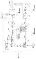
図1は冷陰極管駆動装置を搭載した液晶表示装置の概略構成を示すブロック図である。図1において、100は映像を表示する液晶パネル、200は液晶パネル100に対するバックライト装置(これに冷陰極管210が含まれる)、300は入力された映像信号を液晶駆動信号に変換し、かつバックライト装置200の輝度を映像信号に合わせて制御するための調光データを出力する液晶駆動装置、400はバックライトの駆動および調光制御を行うバックライト駆動制御装置(以下、駆動制御装置と略記する)、500は駆動制御装置400から出力される駆動パルスを電力増幅する電力増幅部、600は電力増幅部500からの駆動パルスに基づいてバックライト装置200における冷陰極管210を駆動する圧電トランス、700はバックライト装置200における冷陰極管210の駆動状況を電気的に検出し、ディジタルデータに変換して駆動制御装置400にフィードバックするデータ変換部、800は液晶駆動装置300と駆動制御装置400とを一体化した1チップLSI、900は駆動制御装置400、電力増幅部500およびデータ変換部700からなる冷陰極管駆動装置である。本発明は、駆動制御装置400をディジタルで実現することにより、液晶駆動装置300と駆動制御装置400とを1チップLSI化するものであり、映像と連動したバックライト調光が可能であるとともに、低コスト化、省スペース化を実現する。
【0109】
以下、いくつかの好ましい実施の形態について具体的に説明していく。説明の便宜上、電源電圧変動を考慮しなくてもよい場合を(A)とし、電源電圧変動を加味する場合を(B)として区分けして説明する。(A)には実施の形態1〜3が含まれ、(B)には実施の形態4〜6が含まれる。
【0110】
(A)電源電圧変動は加味しない冷陰極管駆動装置/液晶表示装置
(実施の形態1)
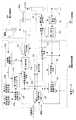
図2は、本発明の実施の形態1に係る液晶表示装置における冷陰極管駆動装置900の構成を示すブロック図である。図2において、1は圧電トランス(図1の圧電トランス600に相当)、2はコイル、3はスイッチングトランジスタ(FET)、4は冷陰極管(図1の冷陰極管210に相当)、5は冷陰極管4に流れる電流を検出し電圧信号に変換する電流検出器、7は電流検出器5から取り出される正弦波状の電圧信号を整流し直流電圧に変換する整流手段(例えばピーク検波回路)、101は整流手段7から出力される電圧をディジタル信号に変換するA/Dコンバータである。なお、電流検出器5につき、図示は抵抗の記号で代表的に表しているが、必ずしも抵抗にとらわれる必要はない。A/Dコンバータ101は、電圧検出精度を得るために十分なビット数を持ち、かつそのサンプルクロックは制御に求められる応答速度を十分に確保できる周波数であるものとする。以下、A/Dコンバータ101の出力ディジタル信号をVadと記す。102はA/Dコンバータ101から出力される検出電圧Vadを所定サンプル数N(サンプル数Nついては後で説明する)の範囲内で平均処理を行う平均処理手段(平滑処理手段の好ましい例)である。以下、平均処理手段102の出力ディジタル信号をVaveと記す。103は平均処理手段102の出力信号Vaveと外部から設定される基準データVrefを比較して両者の誤差を演算し、その結果を誤差データVerrとして出力する誤差電圧演算手段である。104は圧電トランス1の駆動パルスの周波数を設定する周波数設定手段であり、この周波数設定手段104は、前回の周波数設定値Fprevに対し、誤差データVerrに対応する周波数だけ加減してMビットのデータFnextとして出力する。このデータFnextは、駆動パルスN周期期間の分周比を意味するものであり、具体的にはFnext/Nの値が駆動パルスのN周期期間の平均の分周比Divとなる。121は周波数設定手段104から出力される周波数データFnextに基づき、予め定められた周期で制御タイミングパルスを発生させる制御コントローラである。この制御周期は前記駆動パルスN周期のA倍(Aは自然数)の周期に設定される。バースト周波数は、制御コントローラ121から出力されるタイミングパルスと同一周期となる。105は駆動パルスN周期の平均の分周比DivがFnext/Nとなるように分周比を分散し、クロックの分周を行う分周手段である。分周手段105によって圧電トランス1への駆動パルスが生成される。このN周期の駆動パルスからなる周期が分散周期である。122は制御コントローラ121で得られた制御周期パルスをもとに、外部(図1の液晶駆動装置300)から与えられる調光データに含まれる調光レベルに相当するデューティ比のパルス(以下バーストパルスと記す)を出力するバーストパルス発生手段である。このバーストパルスは、“H”レベル期間が前記分散周期より短くならないように設定されている。123は分周手段105で得られた駆動パルスの出力のイネーブル/ディスエーブルを切り換える出力イネーブル手段であり、前記バーストパルスの値が“L”レベルの場合にディスエーブルとなり駆動が停止されるように構成されている。また、平均処理手段102のサンプル数は、分散周期期間のサンプル数と等しくなるように設定されている。
【0111】
図1と図2との対応関係は次のとおりである。コイル2およびFET3は、出力イネーブル手段123から出力される駆動パルスを電力増幅し、圧電トランス1に出力する電力増幅部500を構成している。また、電流検出器5、整流手段7およびA/Dコンバータ101は、冷陰極管4に流れる電流をディジタルデータに変換するデータ変換部700を構成している。また、平均処理手段102、誤差電圧演算手段103、周波数設定手段104、制御コントローラ121、分周手段105、バーストパルス発生手段122、出力イネーブル手段123は、ディジタル回路で構成された駆動制御装置400を構成している。この駆動制御装置400は、データ変換部700から出力された冷陰極管4の電流情報と、外部から入力される調光レベルおよび基準データとに基づいて、圧電トランス1に与える駆動パルスを生成し、冷陰極管4の発光量を制御する。
【0112】
次に、上記のように構成された液晶表示装置の冷陰極管駆動装置900の動作について、まず、全体の駆動概念から説明する。
【0113】
本実施形態の第1の特徴とするところは、制御周期を駆動パルスN周期(分散周期)のA倍(Aは自然数)とし、同一の平均周波数で、A回駆動し、バーストパルスの“H”レベル期間の幅が分散周期より短くならないように設定されていることである。また、第2の特徴とするところは、平均処理手段102のサンプル数Nが分散周期期間のサンプル数と等しくなるように設定されていることである。この2つの特徴の意味するところを図3を参照に説明する。
【0114】
図3は実施形態1の動作概念を説明するためのタイミング図である。図3(A)は制御コントローラ121から出力される制御周期パルス、図3(B)は分周手段105から出力される駆動パルス(その実体は図4(C)に図示されている)、図3(C)はバーストパルス発生手段122から出力されるバーストパルス(これで制御周期内におけるオンデューティを決める)、図3(D)は出力イネーブル手段123から出力される駆動パルス、図3(E)は冷陰極管4に流れる管電流、図3(F)は整流手段7から出力される電流検出信号、図3(G)は平均処理手段102で平均処理を行うデータ範囲を示し、図3(H)は平均処理手段102の出力データVaveを示す。図3では便宜上、上記Aの値を4としている。具体的には、図3(A)の制御周期パルスが示す1制御周期の期間において、図3(B)に示す同じ平均周波数1(あるいは平均周波数2)での繰り返しのパターンが4回となっている。
【0115】
本実施形態における分周手段105は、駆動パルスN周期の平均の周波数で高精度の周波数分解能を得る。このため、分周手段105で得られた駆動パルスで圧電トランス1が駆動され、冷陰極管4に流れる電流を検出する場合、この分散周期単位で検出を行う必要がある。
【0116】
一方、バースト駆動時はON期間の電流が一定になるように制御を行うが、1分散周期単位で制御を行った場合、バーストパルス幅(ON期間)が分散周期より短くなるため、ON時の電流を一定に制御することができなくなる。このため、図3(A)に示すように、同一の平均周波数で複数回駆動(分散周期複数回)し、バーストパルス幅(ON期間)は1分散周期より短くならないように設定し、確実に1分散周期中の平均電流を検出する期間を確保する。このため、電流値検出においても、従来の特許文献2(特開平11-298060号公報)のようにバーストパルスが“H”レベル期間(ON期間)で電流検出するのではなく、本方式は、図3(G)に示すように、バーストパルスが“H”レベル期間(ON期間)で、かつ第1の分散周期期間(4回ある分散周期の最初の期間)でのみ電流を検出する。
【0117】
以上、本実施形態の特徴とするところを説明したが、以下に、図1に示す冷陰極管駆動装置の実際の制御の流れを具体的数値例を示して説明する。
【0118】
ここでは説明を簡単にするために、分散周期を4(N=4)、制御周期を分散周期の4倍(A=4)とする。また、A/Dコンバータ101の分解能を3ビットとし、目標の管電流値は、A/Dコンバータ101から出力されるディジタルデータ換算で6.5とする。A/Dコンバータ101からは小数データは出力されないが、分散周期期間での平均データとして見た場合、小数が存在する。つまり、外部から与える基準データVrefとして、11010(=6.5で、上位3ビット110は整数部6、下位2ビット10は小数部0.5)を与える。今、駆動パルスを生成するための平均の分周比が5.5の場合、周波数設定手段104から出力される周波数データFnextは10110を出力する。このうち上位3ビットが整数部を示し、下位2ビットが小数部を示している。分散周期Nを4と設定しているため、小数部は2ビットとなる。これにより、分周手段105では、図4(C)に示す駆動パルスが出力される。図4(C)において、1つの分散周期に4周期分の駆動パルスが描かれているが、これが分散周期Nである。分周比の分散方法は種々の方法があるが、ここでは特に限定しない。
【0119】
図4(D)に示すバーストパルスが与えられたときの管電流波形を図4(E)に示す。図4(E)に示すように、電流値は駆動パルスの周波数に応じた値になる。図4(F)に、この管電流を電流検出器5により検出し、ピーク検波による整流手段7で得られる出力波形を示す。この例では、分散周期期間のA/D出力データは図4(G)に示すように、“4”,“5”,“4”,“5”のように得られている。平均処理手段102では、この第1の分散周期期間のデータを平均し((4+5+4+5)/4=4.5)、その結果の4.5のデータを出力する。誤差電圧演算手段103では、平均値4.5と外部から与えられる基準データ(=6.5)とを比較し、その差データである2.0(=6.5−4.5)を出力する。次いで、周波数設定手段104では、前回の周波数設定値(=6.5)に誤差電圧演算手段103の出力データ(=2.0)が加えられ、次回の周波数設定データ8.5が出力される。以下、この制御は、管電流が外部から与えられる基準データVrefに等しくなるまで続けられ、ON時の平均電流が一定に保たれる。
【0120】
ここで、ON時の平均電流は、厳密にはバーストパルス幅によって変化する。これを図5を用いて説明する。図5において(A)は分周比の分散例で、分周比に応じた電流が冷陰極管4に流れる。本例の電流検出期間は、図5に示す通り第1の分散周期期間のみであり、この間の平均分周比は4.5である。
【0121】
ところで、例えばバーストパルスが図5(B)に示すパルス幅の場合、この間の平均分周比は約4.43(≒31/7)となる。また、図5(C)に示すパルス幅の場合、その平均分周比は4.5(≒27/6)であり、図5(D)に示すパルス幅の場合、その平均分周比は4.4(≒22/5)となる。このように実際には、流れている平均電流値と検出電流値は異なる。バーストパルス幅が小さくなるにつれてその誤差が大きくなる。
【0122】
しかし、実際に輝度に与える影響はバーストパルス幅による調光精度の方が大きく、図5の例では、バーストパルス幅による輝度レベル差は、それぞれ1/16=6.75%であるのに対し、電流検出誤差による影響は、(B)の場合が(4.5−4.43)/4.5=1.5%、(C)の場合は0%、(D)の場合は(4.5−4.4)/4.5=2.2%でしかない。さらに、実際には、分周比は4や5よりもはるかに大きい。例えば、10MHzのクロックで100KHzのパルスを生成する場合は100分周となる。図3(D)で駆動パルスを細かく描いていることは、そのことを示唆している。また、分散周期も4よりはるかに多い(例えば256分散)。このため、実際にはその検出誤差はほとんど無視できるレベルになる。
【0123】
以上の説明のように本実施形態では、制御周期を駆動パルスN周期(分散周期)のA倍(Aは自然数)とし、同一の平均周波数で、A回駆動し、平均処理手段102のサンプル数Nが分散周期期間のサンプル数と等しくなるようにすることにより、駆動パルスの周波数分散によるディジタル駆動方式においても、バースト調光を実現できる。これにより、他のLSIと1チップ化による低コストかつ省スペース化に有利なディジタル方式での冷陰極管駆動装置を提供でき、小型映像機器のさらなる小型化に対する効果は大きい。
【0124】
なお、本実施形態では、電流検出期間を第1の分散周期期間としているが、電流検出期間については、特にこの期間でなくともよい。冷陰極管4は、電圧が印加されたときに、直ぐに管電流が流れて点灯を始めるわけではなく、若干の遅延が生じるからである。バースト駆動時は図6(E)に示すように、OFFからONに移行した後、しばらくしてから管電流が流れ始めるため、電流検出期間を上記第1の分散周期期間とすれば、正確な平均電流を検出できず都合が悪くなる。このため、図6(F)に示すように、駆動再開から点灯までの遅れ時間を考慮して、検出幅を変えずに検出位置をずらせばよい。
【0125】
更にこの電流検出期間は分散周期1周期幅である必要はなく、図7に示すようにバーストパルス幅に応じて、分散周期×2の幅、分散周期×3の幅と、電流検出期間を変化させても良い。このときのブロック図を図8に示す。
【0126】
図8において、124はバーストパルス発生手段122からのバーストパルスと制御コントローラ121からの制御タイミングパルスから、検出範囲を演算する検出幅調整手段であり、バーストパルス幅に応じて検出範囲を調整する。この場合、調光レベルが大きくなるほど電流検出精度が向上する。
【0127】
なお、本実施形態では、1分散周期期間の冷陰極管4に流れる平均電流を検出するために平均処理手段を用いたが、特に厳密な輝度精度を必要としない場合には通常のフィルタ手段に置き換えることができる。この平均処理手段やフィルタ手段を統括して平滑処理手段ということができる。特許請求の範囲では、平滑処理手段としている。
【0128】
また、駆動制御装置400を構成する各要素〜平均処理手段102、誤差電圧演算手段103、制御コントローラ121、周波数設定手段104、バーストパルス発生手段122、分周手段105および出力イネーブル手段123、さらに検出幅調整手段124〜については、ハードウエアで構成してもよいし、ソフトウエアで構成してもよいし、あるいはハードウエアとソフトウエアとのハイブリッド構成としてもよい。
【0129】
(実施の形態2)
次に、本発明の実施の形態2に係る冷陰極管駆動装置について説明する。冷陰極管4に流れる平均電流を正しく検出するには、最低1分散周期の検出範囲が必要である。実施形態1では、バーストパルス幅を分散周期幅より大きくする必要があり、調光レベルの下限に制約がある。本実施形態2は、これを解決する。
【0130】
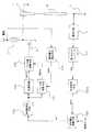
図9は、実施形態2に係る冷陰極管駆動装置の構成を示すブロック図である。図9において、104aは圧電トランス1の駆動パルスの周波数を設定する周波数設定手段であり、前回の周波数設定値Fprevに対し誤差データVerrに対応する周波数だけ加減してMビットのデータFnextとして出力する。図2に示す実施形態1で説明した周波数設定手段104と異なるところは、小数を含む分周比を示すMビットのデータのうち、小数部の有効ビット数が、実施形態1では固定であるのに対し、本実施形態2では可変となっていることである。この小数部の有効ビット数の変え方については後で明確にする。121aは周波数設定手段104aから出力される周波数データFnextに基づき制御を行う制御コントローラであり、その制御周期は前記駆動パルスN周期のA×k倍(Aは自然数、kの値は分散周期に応じて変化する値)の周期に設定されている。
【0131】
105aは駆動パルスN周期の平均の分周比DivがFnext/Nとなるように分周比を分散しクロックの分周を行う分周手段で、圧電トランス1の駆動パルスが生成される。ここで、図2に示す実施形態1による分周手段105と異なるところは、分散周期を決めるNの値を分周手段外部から設定できるように構成されていることである。125はバーストパルス発生手段122から出力されるバーストパルスの幅から、分散数を決定し、分周手段104aに分散数Nの値を出力するとともに、周波数設定手段104aに切換信号を出力する。さらに制御コントローラ121aに対してkの値を設定する。このkの値は、分散数Nの値が変わっても制御周波数が変わらないように、(k×N)の値が一定になるように決められる。その他の構成については図2に示す実施形態1の場合と同様であるで、説明を省略する。
【0132】
次に、上記のように構成された冷陰極管駆動装置の特徴について説明する。本実施形態の特徴は、バーストパルス幅に応じて、分散数Nを変え(つまり分散周期が変わる)、分散周期が変わっても制御周期(つまりバーストパルスの周期)が変わらないように、同一の平均周波数で駆動する回数を同時に変えることである。
【0133】
この様子を図10に示す。図10(A)は、駆動パルスN周期で平均の周波数精度を得るように分周比が分散されている。このとき、同一の平均周波数で4回駆動される。図10(B)は駆動パルスN/2周期で平均の周波数精度を得るように分周比が分散されている。このとき、上記図10(A)と同一の制御周期となるように、同一の平均周波数で8回駆動される。
【0134】
冷陰極管4に流れる平均電流を正しく検出するには、実施形態1で説明した通り、最低1分散周期の検出範囲が必要である。図10(A)の場合、1分散周期期間の検出を確保するには、バーストパルスのデューティは最低25%必要であるのに対し、図10(B)では12.5%でよい。一方で、電流精度は分散数が多い方が高いため、図10(B)の場合、同図(A)に比べて半分の精度になる。
【0135】
しかしながら、調光精度を必要とするのは、通常、映像鑑賞として使用される約50〜100%の調光レベルであり、低輝度部では、高輝度部ほど調光精度を必要としない。低輝度モードは待機モードやOSD(オンスクリーンディスプレイ)のみしか表示しないときに消費電力を削減するために使用される。そこで、低輝度の場合(バーストパルスの幅が所定以下になった場合)は、分散数を小さくして、かつバースト周波数が変わらないように、同一周波数で駆動する回数を多くする。
【0136】
以上説明したように、本実施形態では、バーストパルス幅に応じて分散数を変えることにより、調光レベルを小さくすることが可能であり、調光範囲の大幅拡大が可能になる。
【0137】
なお、ここでは調光レベルを小さくするために分散数を変える方法で説明したが、もちろん、バースト周波数低下によるフリッカが回避できる場合は、バースト周波数を変える手法がある。この場合、図11に示すように、分散数は一定のまま、同一周波数で駆動する分散周期の回数Aを変えればよい。
【0138】
この場合の実施の形態を図12に示す。図12において、121bは同一周波数で駆動する回数Aの値を制御コントローラ外部から設定できるように構成された制御コントローラであり、126はバーストパルスに連動して制御コントローラ121bの駆動回数Aの値を設定する制御周期設定手段であり、所定以下の調光レベルになった場合にAの値を大きくし、MIN調光レベルを小さくできるようにしている。図12に示す構成にすることにより、バースト周波数(ON・OFFの周波数)は変化するが、実施形態1の場合に比べ大幅に調光範囲を拡大できる効果を有する。
【0139】
ここで、特に言及しなかったが、本実施形態においても、実施形態1で説明したバーストパルスのデューティに応じて検出範囲を変える手段や、平均処理を単純なフィルタ手段に変えることとの併用なども可能である。
【0140】
なお、駆動制御装置400を構成する各要素〜平均処理手段102、誤差電圧演算手段103、制御コントローラ121a、周波数設定手段104a、バーストパルス発生手段122、分周手段105a、出力イネーブル手段123および分散数調整手段125、さらに制御周期設定手段126〜については、ハードウエアで構成してもよいし、ソフトウエアで構成してもよいし、あるいはハードウエアとソフトウエアとのハイブリッド構成としてもよい。
【0141】
(実施の形態3)
次に、本発明の実施の形態3に係る冷陰極管駆動装置について説明する。
【0142】
図13は、本発明の実施の形態3に係る冷陰極管駆動装置の構成を示すブロック図である。本実施形態は、調光レベルが小さい場合でも始動時の点灯性能および点灯品位を低下させることのない冷陰極管駆動装置を提供するものである。
【0143】
図13において、14は圧電トランス1の出力電圧を検出するための電圧検出手段、15は電圧検出手段14で検出した圧電トランス1の検出電圧をON・OFFするための遮断手段で、OFFのときには遮断手段15の出力電圧が“L”レベルになるように構成されている。7aは遮断手段15から出力される圧電トランス1の出力電圧検出と、電流検出器5から出力される管電流検出のMAX検出を行うピーク検出手段である。電流検出器5、ピーク検出手段7a、電圧検出手段14、遮断手段15およびA/Dコンバータ101により、冷陰極管4に流れる電流と圧電トランス1の出力電圧を時分割で検出し、ディジタルデータに変換するデータ変換部700aを構成している。127はA/Dコンバータ101のディジタル出力データから点灯検出を行う点灯検出手段で、点灯検出を行うために遮断手段15を所定の周期でON・OFF制御している。点灯検出手段127は、遮断手段15に対して検出切換パルスを出力し、また後述の調光レベル切換手段128および制御周期切換手段129に対して点灯検出パルスを出力するように構成されている。この点灯検出手段127については、後で詳細に説明する。
【0144】
128は点灯検出手段127から出力される点灯検出パルスに基づいてバーストパルス発生手段122に与える調光レベルを切り換える調光レベル切換手段であり、始動時は、あらかじめ設定された調光レベルを出力するように構成されている。なお、ここでは、始動時の調光レベルを100%(連続駆動)とする。
【0145】
121bは同一周波数で駆動する回数Aの値を外部から設定できるように構成された制御コントローラであり、図12に示す制御コントローラと同一である。126aは制御コントローラ121bの第1の制御周期を設定する第1の制御周期設定手段であり、126bは制御コントローラ121bの第2の制御周期を設定する第2の制御周期設定手段である。129は点灯検出手段127から出力される点灯検出パルスによって第1の制御周期設定手段126aから出力される制御周期情報と第2の制御周期設定手段126bから出力される制御周期情報を切り換えて出力する制御周期切換手段である。このように、周波数設定手段104に出力する制御周期を起動時と点灯時で切り換えるように構成されている。ここで、第1の制御周期設定手段126aは始動時の制御周期を設定し、その周期は分散周期2回(上記Aの値が2になる)に設定され、第2の制御周期設定手段126bは点灯時の制御周期を設定し、点灯時は実施形態1と同様、分散周期4回(上記Aの値が4になる)に設定されているものとする。その他の構成については、図2を用いて説明した実施形態1に係る構成と同様であるので説明は省略する。
【0146】
このように構成された図13に示す平均処理手段102、誤差電圧演算手段103、周波数設定手段104、制御コントローラ121b、分周手段105、バーストパルス発生手段122、出力イネーブル手段123、点灯検出手段127、調光レベル切換手段128、第1の制御周期設定手段126a、第2の制御周期設定手段126bおよび制御周期切換手段129からなる部分で駆動制御装置400cを構成する。
【0147】
次に、図13に示す本実施形態に係る構成の冷陰極管駆動装置の特徴について説明する。本実施形態の特徴とするところは以下の点である。
【0148】
(1)始動時は点灯性能を確保できる連続駆動とし、点灯検出後すみやかに所望の調光レベルに移行する。
【0149】
(2)点灯直後の輝度の変動を抑えるため、MIN調光時のバーストパルス幅以内で点灯検出を行う。
【0150】
特に、(2)を実現するために、始動時と点灯時の制御周期を切り換え、始動時には制御周期を短くするようにしている。
【0151】
まず、図14に始動時と点灯時の制御周期を示す。図14(A)は始動時の1制御期間の駆動パルスを示し、同一の平均周波数で2回駆動する。図14(C)は点灯時の1制御期間の駆動パルスを示し、同一の平均周波数で4回駆動する。図14(B)は始動時の電圧(電流)検出期間で、遅延Aだけずらして検出を行う。図14(D)は点灯時の電圧(電流)検出期間で始動時と同様に遅延Aだけずらして検出を行う。
【0152】
次に、始動時の制御から点灯時の制御に切り換えるための点灯検出手段127の動作について説明する。図15は始動時における点灯検出手段127の動作を示す図で、図15(C)は電圧検出手段14から出力される圧電トランス1の出力電圧検出信号、図15(D)は電流検出器5から出力される電流検出信号で、始動時は冷陰極管4が点灯していないため、電流は流れていない。制御周期切換手段129は第1の制御周期設定手段126aを選択しており、制御周期として同一駆動2回分が設定されている。調光レベル切換手段128は連続駆動の調光レベルを選択してバーストパルス発生手段122に出力する。
【0153】
図15(E)は点灯検出手段127から遮断手段15へ出力される点灯検出のための検出パルスである検出切換パルスで、この検出切換パルスが“H”レベルのときに遮断手段15がOFFされて、ピーク検出手段7aからは電流検出信号のピーク値が出力される。点灯検出は検出切換パルスが“H”レベルのときのピーク検出手段7aの出力レベルで判断される。つまり、点灯していないときは管電流は流れていないため、ピーク検出手段7aの出力はゼロレベルになるのに対し、点灯を開始すれば管電流が流れるため、ピーク検出手段7aの出力は管電流レベルに相当する電圧値が出力される。したがって、検出切換パルスが“H”レベルのときに、ピーク検出手段7aの出力が“L”レベルのときは点灯しておらず、所定レベル以上のときは点灯していると判断できる。
【0154】
図15では、時刻T1において点灯を開始し、図15(D)のように管電流が流れ出している。次に、時刻T2において図15(E)の検出切換パルスが“H”レベルのとき、図15(F)のピーク検出手段7aの出力は管電流に相当するレベルとなって点灯検出され、図15(G)の点灯検出パルスが“L”レベルから“H”レベルへと移行している。
【0155】
次に、図16に始動時の制御から点灯時の制御に移行するときの各部波形を示す。図16に示すように時刻T1で冷陰極管4が点灯を開始し、管電流が流れ出す。直後の時刻T2で検出切換パルスによって点灯が検出され、点灯検出パルスが“L”レベルから“H”レベルへと移行する。
【0156】
時刻T2で点灯検出パルスが“H”レベルになると、制御周期切換手段129は第2の制御周期設定手段126bを選択する状態に切り換えられる。これによって、制御周期が同一駆動2回分から4回分に切り換わり、同時に調光レベル切換手段128は、連続駆動の調光レベルに代えて、外部から与えられる調光レベルに切り換えられ、バーストパルス発生手段122に出力する。これによって、図16(H)に示すように、時刻T2からバーストパルスが出力され、バースト調光に切り換わる。この過程で、点灯前後の管電流は図16(D)に示すようにイレギュラー期間が存在し、このイレギュラー期間に相当する輝度変化が発生する。しかし、この期間は最大で点灯時の制御周期の50%に抑えられており、実使用において点灯時の輝度変化が大幅に改善される。また実際には、点灯時の制御周期は4ではなく、例えば、バースト周波数を150Hz、圧電トランス1の駆動周波数を150KHz、分散数を100とした場合、分散周波数(1/分散周期)は150KHz/100=1.5KHzとなり、バースト周波数を150Hzとするには、制御周期は分散周期の10倍となる。この場合、最大のイレギュラー期間は図17に示すように、点灯時の制御周期の20%になり、実際、このときの輝度レベル変化は無視できる。
【0157】
さらに、始動時の分散数を点灯時の分散数より小さくするようにすれば、このイレギュラー期間は一層短くなり、良好な点灯性能が得られる。この例を図18に示す。
【0158】
図18において、125aは周波数設定手段104aの分散周期を切り換える分散数調整手段である。周波数設定手段104aは図9に示す実施形態2における周波数設定手段と同一の動作を行い、分散数調整手段125aの出力に応じて分散数が変わる。図9に示す実施形態2の分散数調整手段125と異なるところは、実施形態2の分散数調整手段125は、バーストパルス発生手段122からのバーストパルスの幅すなわち調光レベルに応じて分散数を変える仕組みであったが、本実施形態における分散数調整手段125aは点灯時と起動時で切り換える仕組みとなっている。このため、点灯検出手段127からの点灯検出パルスが分散数調整手段125aに入力されている。その他の動作は、図13に示す例と同一である。
【0159】
図19に起動から点灯に至るまでの各部波形を図示するが、本実施形態では、起動時の点灯検出周期が図13の実施形態に対し1/2になるため、起動時の点灯時のイレギュラー期間が図13の例に比べて半分になる。
【0160】
以上説明したように、本発明による実施形態3に係る冷陰極管駆動装置によれば、始動時を連続駆動とすることにより、点灯性能を劣化させずにバースト調光に移行できる。また、始動時と点灯時の制御周期を変えることにより、または分散数を変えることにより、点灯時の輝度変化がほとんど無視できるレベルにまで改善でき、点灯品位を大幅に改善できる効果を有する。
【0161】
なお、駆動制御装置400cを構成する各要素〜平均処理手段102、誤差電圧演算手段103、制御コントローラ121b、周波数設定手段104、バーストパルス発生手段122、分周手段105、出力イネーブル手段123、点灯検出手段127、調光レベル切換手段128、第1の制御周期設定手段126a、第2の制御周期設定手段126bおよび制御周期切換手段129、さらに分散数調整手段125a〜については、ハードウエアで構成してもよいし、ソフトウエアで構成してもよいし、あるいはハードウエアとソフトウエアとのハイブリッド構成としてもよい。
【0162】
ここで、上記実施形態1〜3の他の特徴は、駆動制御装置の処理がディジタル化可能なため、ソフトウエアによる制御も可能である。つまりマイコンプログラムとして構築可能なため、容易にシステムが構築可能である。
【0163】
図20は実施形態1の場合を例にフローチャートを示したものである。
【0164】
図20において、ステップS1はデータ読み込みを行う処理、ステップS2はデータ取り込み回数が所定の回数に達したかを判断し、所定回数に達していない場合はステップS1に戻り、再度データを取り込む。所定回数に達すれば、ステップS3で取得したデータの平均を演算する。ここで所定回数とは分散周期の整数倍の駆動パルス数である。これらステップS1〜S3は図2に示す実施形態1の平均処理手段102に相当する。ステップS4は外部から与えられる基準データと平均データを比較する。ステップS4は実施形態1の誤差電圧演算手段103に相当する。ここで基準データの方が大きければ、ステップS5において次の分周比を大きく(つまり駆動周波数が低くなるように)設定し、冷陰極管4に流れる電流が大きくなるようにする。他方、基準データの方が小さければ、ステップS6において分周比を小さく設定し、逆に冷陰極管4に流れる電流が小さくなるように設定する。このステップS5,S6は図2の周波数設定手段104に相当する。ステップS7では設定された分周比でクロック(ソフト上ではマイコンクロックあるいはマイコンクロックから作られたタイマーに相当)を分周する。これは図2の分周手段105に相当する。ステップS8は分周されたデータ(駆動パルスに相当)の数をカウントし、分散の回数が所定回数になったかどうかを判断し、所定回数になっていなければステップS7に戻って再度同じ周波数設定で分周を行う。この部分が図2の制御コントローラ121に相当する。その後、ステップS9では外部から与えられる調光レベルをもとにバーストパルス幅を演算し、バーストパルスが“H”レベルのときに出力ポートから上記分周されたデータを出力し、他方、“L”レベルのときは出力ポートを“L”レベルにする。この部分が図2のバーストパルス発生手段122に相当する。ステップS10〜S12が図2の出力イネーブル手段123に相当する。
【0165】
以上、図2の実施形態1の場合を例に簡単にソフト動作を説明したが、特にここでは具体例を示さないが、他の実施形態においても同様にソフトウエアによる処理が可能である。
【0166】
(B)電源電圧変動を加味する冷陰極管駆動装置/液晶表示装置
ところで、バックライトを駆動させるために圧電トランスの駆動に求められるものは、基本的には、調光機能、低電力(高い電力変換効率)等である。さらにノートパソコンやディジタルビデオカメラなどの携帯機器に用いる場合、安定した電源が得られないバッテリ電源を考慮し、広範囲な電源電圧で安定した点灯、安定した電力変換効率が望まれる。
【0167】
上記の課題を改善するため、特許文献3(特開平8−33349号公報)では、電源電圧に応じて駆動パルスのパルス幅(デューティ比)を変えて、広い電源電圧範囲に対応する方法が示されている。以下、この方式をデューティ制御と記す。
【0168】
特許文献3の原理を図48に基づいて簡単に説明する。図48において、(A)は圧電トランスのスイッチングトランジスタであるFETのゲートに与える駆動パルスで、(B)は駆動パルスにより発生したFETのドレイン電圧を示している。このドレイン電圧は電源電圧により変化する。電源電圧を高くすると、(C)に示すように、ドレイン電圧の振幅が大きくなり、ドレイン電圧が0Vになる前にFETがONする。このような状態になると、FETがONした瞬間にドレインとGNDが短絡することにより大きな電流(サージ電流)が流れる。このことは、FETの破壊につながる。あるいは、この急激な電流が圧電トランスに流れると、圧電トランスの破壊につながる。このため、電源電圧に応じて駆動パルス幅を調整し、急激なサージ電流が流れないようにする。
【0169】
図48(D)は、電源電圧を大きくした場合の駆動パルスを示し、(A)の駆動パルスに対してパルス幅を小さくしている。これにより、(E)に示すようにドレイン電圧が0VのところでFETをONするようにする。この方法により広い電源電圧でも、ロスの少ない駆動が可能になる。
【0170】
上述したように、特許文献3では、駆動パルスのデューティ比を電源電圧に応じて変えることにより、広い電源電圧範囲での使用が可能となる。
【0171】
しかし、これをディジタル駆動方式で行う場合、10MHz程度のクロックではデューティ比率の分解能が粗く、十分な性能が得られない(クロックを高くすれば分解能は得られるが、回路電力の増加、輻射妨害の増加で実用的でなくなる)。広い電源電圧範囲で良好な性能を求める場合、駆動パルスのデューティ比率はできるだけ小刻みに調整できることが望ましい。少なくとも電源電圧0.1V刻みで可変できることが望ましい。
【0172】
図49にディジタル駆動方式でデューティ調整する場合の様子を示しており、クロックの周波数が低いほど分解能は粗くなり、理想から大きくずれるポイントが出てくる。
【0173】
実例を挙げて説明する。10MHzのクロックを100分周し、100kHzの周波数の駆動パルスを生成した場合、生成されたパルスのパルス幅はクロック1周期幅〜99周期幅まで1周期毎に調整可能である。つまり、デューティ比は1%刻みで調整できる。
【0174】
しかしながら、例えば理想のデューティカーブが電源電圧5V〜10Vでデューティ30%〜20%であった場合、1%刻みでは、10段階調整(0.5V刻み)しかできないことを意味する。これでは、十分な性能は得られない。
【0175】
本発明の実施の形態4以下では、上記した課題に鑑みてなされたもので、ディジタル駆動方式で効率劣化のないデューティ制御方式を提案し、広範囲な電源電圧に対応する冷陰極管駆動装置を実現することを目的とする。
【0176】
(実施の形態4)
図21は、本発明の実施の形態4における冷陰極管駆動装置の構成を示すブロック図である。図21において、1は圧電トランス、2はコイル、3はスイッチングトランジスタ(FET)、4は冷陰極管、5は冷陰極管4に流れる電流を検出し電圧信号に変換する電流検出器である。なお、電流検出器5につき、図示は抵抗の記号で代表的に表しているが、必ずしも抵抗にとらわれる必要はない。7は電流検出器5から取り出される正弦波状の電圧信号を整流し直流電圧に変換する整流手段、101は整流手段7から出力される電圧をディジタル信号に変換するA/Dコンバータ(第1のA/Dコンバータ)であり、電圧検出精度を得るために十分なビット数を持ち、かつそのサンプルクロックは制御に求められる応答速度を十分に確保できる周波数であるものとする。以下、A/Dコンバータ101の出力ディジタル信号をVadと記す。102はA/Dコンバータ101から出力される検出電圧Vadを所定サンプル数の範囲内で平滑処理を行う平滑処理手段で、以下、平滑処理手段102aの出力ディジタル信号をVaveと記す。103は平滑処理手段102aの出力信号Vaveと外部から設定される基準データVrefを比較して両者の誤差を演算し、誤差データVerrとして出力する誤差電圧演算手段である。104は圧電トランス1の駆動パルスの周波数を設定する周波数設定手段であり、前回の周波数設定値Fprevに対し誤差データVerrに対応する周波数だけ加減してMビットのデータFnextとして出力する。このFnextは、駆動パルスN周期期間の平均の分周比を意味するものである。105は駆動パルスN周期の平均の分周比DivがFnext/Nとなるように分周比を分散し、クロックの分周を行う分周手段で、圧電トランス1に対する駆動パルスが生成される。以下、分周手段105から出力される分周比分散の駆動パルスをpzplsと記す。
【0177】
図22(B)に分周手段105で生成された分散パルスpzplsの例を示し、同図(C)に同時に得られる分周比データを示す。また、同図(A)はクロックである。
【0178】
ここまでの構成は特許文献1(特開2000−133485号公報)に記載された構成と同一であり、動作も同一である。本実施形態の特徴は以下の手段106〜108を含んでいることである。
【0179】
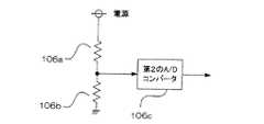
106は電源電圧を検出しディジタル値として出力する電源電圧検出手段であり、例えば図23に示すように構成される。図23において、106a、106bは抵抗であり、電源電圧を分圧し、第2のA/Dコンバータ106cの入力ダイナミックレンジに適合する電圧に変換する。第2のA/Dコンバータ106cは入力された電圧をディジタル値に変換するものである。以下、電源電圧検出手段106の出力信号をVpwrと記す。
【0180】
次に、107は周波数設定手段104で得られる周波数データFnextと電源電圧検出手段106で得られる電源電圧情報Vpwrから予め決められた電源電圧と駆動パルスのデューティ値との関係に基づいて駆動パルスのデューティ値(以下、Vdutyと記す)を算出するパルス幅演算手段である。パルス幅のデューティ比は、“H”レベルの期間と“L”レベルの期間の比である。このパルス幅デューティ比がパルス幅情報に相当する。
【0181】
例えば、電源電圧と駆動パルスのデューティ値との関係の一例を図24に示すが、パルス幅演算手段107の演算方式は種々の方式があり、ここでは特に限定しない。この種々の方式とは例えば、予め電源電圧Vpwrとデューティ値Vdutyの関係をROM(リードオンリーメモリ)に格納しておくROM方式、あるいは、図24に示す曲線を線形近似で演算する方式などである。
【0182】
108はパルス幅演算手段107から出力されるデューティ値Vdutyに基づき、パルス幅の調整を行うパルス幅調整手段である。
【0183】
図25はパルス幅調整手段108の具体的な構成例を示したものである。図25において、108aは分散パルスpzplsを入力してデューティ値Vdutyの値に応じたパルス幅に変換するパルス幅整形手段(デコード手段)である。
【0184】
ここで、デューティ値VdutyをAビットのディジタルデータとしたとき、パルス幅整形手段108aで参照されるのは上位A−1ビットのデータとし、このA−1ビットの値に等しいパルス幅の信号が出力されるものとする。
【0185】
以下、0ビット目からA−1ビット目のAビットのバス幅を持つ信号Vdutyの上位A−1ビットのデータを表す記法として、Vduty[A-1:1]と記す。また、最下位ビットのデータをVduty[0]と記す。
【0186】
図26にパルス幅整形手段108aの入出力波形を示す。図26(D)に示すように、出力されるパルスのパルス幅は同図(C)に示すVduty[A-1:1]の値と等しくなる。
【0187】
図25中の108bはパルス幅整形手段108aの出力信号をラッチ出力するDフリップフロップ(以下、DFFと記す)で、この出力信号を元パルスpzplsaと記す。108cは元パルスpzplsaをクロックの立下りエッジでラッチ出力するDFFで、この出力信号をパルスpzplsbと記す。108dはORゲートで、このORゲートの出力信号を拡張パルスpzplscと記す。これらDFF108cとORゲート108dでパルス幅拡張手段108gを構成している。すなわち、遅延させた上で論理和をとることにより、パルス幅を拡張している。108eはVduty[0]が1のときは拡張パルスpzplscを出力し、Vduty[0]が0のときは元パルスpzplsaを出力するセレクタである。このセレクタ108eの出力がFET3を駆動する駆動パルスpzdrvとなる。また、108fはクロックを反転するためのインバータである。このインバータ108fでクロックを反転して、DFF108cではクロックの立ち下がりエッジでのラッチを行う点に注目する必要がある。
【0188】
次いで、図21および図25に示すように構成された冷陰極管駆動装置の動作を説明する。本実施形態の特徴とするところを中心に説明する。
【0189】
本実施形態の特徴とするところは、クロックの立下りエッジを用い、駆動パルスpzdrvのパルス幅分解能を2倍にする技術である。
【0190】
通常のディジタルLSIにおいては、設計から検証、製造までの手順が確立された同期回路で構成されるのが一般的である。このため、このような同期回路では非同期処理となるクロックの立下りエッジは使われない。しかしながら、この非同期処理も、LSIの出力ピンの直前では比較的容易に検証が可能であるため、この立下りエッジを使う処理を回路の最後段で行えるようにしている。
【0191】
つまり、パルス幅演算手段107から出力されるパルス幅情報のデューティ値Vdutyの値を上位ビットと下位ビットに分け、まず第1段階ではデューティ値Vdutyの上位ビットを使い、通常の同期処理で所定のパルス幅のパルスを生成し、さらに第2段階ではデューティ値Vdutyの下位ビットを使い、クロックの立下りエッジを用いた処理でさらに分解能を上げて、第2段階の処理の後では同期処理は行わないように構成したものである。
【0192】
図27は、デューティ値Vdutyから2段階のパルス幅生成の波形を示した図で、(A)はクロック、(B)は分周手段105からの分散パルスpzpls、(C)はデューティ値Vduty、(D)はデューティ値Vdutyの上位A−1ビットのデータVduty[A-1:1]、(E)はVdutyの最下位ビットのデータVduty[0]である。
【0193】
例えば、Vdutyが10すなわち2進数表記で(1010)2の場合、上位A−1ビットのデータVduty[A-1:1]は(101)2で5であり、最下位ビットのデータVduty[0]は(0)2で0である。また、Vdutyが9すなわち2進数表記で(1001)2の場合、上位A−1ビットのデータVduty[A-1:1]は(100)2で4であり、最下位ビットのデータVduty[0]は(1)2で1である。
【0194】
また、図27において、(F)はパルス幅整形手段108aから出力されたパルスがクロックの立ち上がりエッジでラッチされた元パルスpzplsa、(G)は元パルスpzplsaがクロックの立下りエッジでラッチされたパルスpzplsbである。
【0195】
まず、第1段階のパルス幅生成処理はパルス幅整形手段108aで行われる。このときのパルス幅はVdutyを2で割り、小数部を切り捨てたデータであるVduty[A-1:1]となる。
【0196】
例えば、Vduty=10のときはVduty[A-1:1]=5であり、Vduty=9のときはVduty[A-1:1]=4となる。
【0197】
DFF108cおよびORゲート108dからなるパルス幅拡張手段108gでは、元パルスpzplsaのパルス幅をクロックの0.5周期分広くする処理が行われる。これにより、得られた拡張パルスpzplscを図27(H)に示す。
【0198】
次いで、セレクタ108eでは、Vduty[0]の値が1のとき、つまり切り捨てられた値が1のときは0.5周期幅広の拡張パルスpzplscを出力し、逆にVduty[0]の値が0のとき、つまり切り捨てられた値がないとき(0のとき)は元パルスpzplsaを出力する。これにより、得られる駆動パルスpzdrvのパルス幅は図27(I)に示すように5周期幅、4.5周期幅、5周期幅と、Vdutyの値に応じたパルス幅が得られる。すなわち、Vdutyが10のときは、その2分の1の5となり、Vdutyが9のときも同じく2分の1の4.5が得られる。四捨五入などの丸め処理がなく、正しく2分の1に対応し、分解能が向上されている。
【0199】
この駆動パルスpzdrvは同期回路を介在することなく、そのままピンから出力されるので、ディジタルLSIの設計、検証に問題を来すことはない。
【0200】
以上のように、本実施形態では、ディジタルLSIの設計手法から逸脱することなく、クロックの立下りエッジを用いた2倍精度のパルス幅分解能が得られ、これにより、ディジタル駆動方式においても広範囲な電源電圧で最適なパルス幅の駆動パルスが得られる。これは、圧電トランスを駆動する上で、効率改善による消費電力削減、サージのためにFETや圧電トランスの破壊されることを防止することにつながり、その効果は大きい。
【0201】
上記実施形態では、クロックの立下りエッジを利用した方法であったが、この代わりに遅延素子を組み合わせて使うこともできる。
【0202】
図28は遅延素子とクロックの立下りエッジを使う方式を組み合わせたパルス幅調整手段の例である。
【0203】
図28において、108g1、108g2は遅延素子で、その遅延量はクロック1周期の1/4に設定されている。108d1〜108d3はORゲート、108e1〜108e3はセレクタである。他の構成要件は図25に示すパルス幅調整手段と同一である。ただし、図25ではデューティ値VdutyはAビットとし、Vduty[A-1:1]がパルス幅整形手段108aに入力され、Vduty[0]でクロックの立下りエッジによるパルス幅の微調整が行われていたが、図28では、デューティ値VdutyをA+1ビットとし、上位A−1ビットであるVduty[A:2]がパルス幅整形手段108aに入力され、デューティ値Vdutyの下位2ビットであるVduty[1:0]で微調整が行われるようにしている。
【0204】
以下、図29に示す各部タイミング波形図を基に説明する。
【0205】
図29において、(F)はVduty[A:2]の値で決まるパルス幅の駆動パルスを発生するパルス幅整形手段108aの出力をクロックの立上りエッジでラッチ出力されたパルスpzplsaであり、概略上記図25の実施形態4で説明したものと同一である。このパルスpzplsaが遅延素子108g1により、クロックの1/4周期分だけ遅延し、図29(G)に示す波形が得られる。また、同図(H)はパルスpzplsaをクロックの立下りエッジでラッチされたパルスpzplsbで、これは上記図25で説明したものと同一である。さらに、このパルスpzplsbが遅延素子108g2で遅延され、パルスpzplsbに対しクロックの1/4周期だけ遅れた図29(I)の信号が得られる。これらの信号がそれぞれORゲート108d1〜108d3を通ることにより、図29(J)〜(L)に示すように元のパルスpzplsaに対しパルス幅が1/4クロック周期の分解能で徐々に広くなる3つの拡張パルスpzplsc1、pzplsc2、pzplsc3が得られる。セレクタ108e1〜108e3はVduty[1:0]の値に応じてパルスpzplsaおよびpzplsc1〜pzplsc3を切り換えてFET3へ出力するもので、Vduty[1:0]が0のときはパルス幅が一番狭いパルスpzplsaが選択され、Vduty[1:0]が1のときはパルス幅が2番目のパルスpzpls1が選択され、Vduty[1:0]が2のときはパルス幅が3番目のパルスpzpls2が選択され、Vduty[1:0]が3のときにパルス幅が一番広い拡張パルスpzplsc3が選択される。FET3に出力される駆動パルスpzdrvを図29(M)に示す。
【0206】
具体例では、Vduty=21=(10101)2で、Vduty[A:2]=(101)2=5、Vduty[1:0]=(01)2=1であるが、このとき駆動パルスpzdrvの周期は5.25周期となり、これは21を4で割った値に丁度等しくなっている。また、Vduty=20=(10100)2で、Vduty[A:2]=(101)2=5、Vduty[1:0]=(00)2=0であるが、このとき駆動パルスpzdrvの周期は5周期となり、これは20を4で割った値に丁度等しくなっている。また、Vduty=19=(10011)2で、Vduty[A:2]=(100)2=4、Vduty[1:0]=(11)2=3であるが、このとき駆動パルスpzdrvの周期は4.75周期となり、これは19を4で割った値に丁度等しくなっている。図示はしていないが、Vduty=18=(10010)2で、Vduty[A:2]=(100)2=4、Vduty[1:0]=(10)2=2であるが、このとき駆動パルスpzdrvの周期は4.50周期となり、これは18を4で割った値に丁度等しくなっている。
【0207】
このように上記図28の構成では、クロックの立下りエッジを使ってのパルス幅分解能向上に加え、さらにクロックの1/4周期分だけ遅延する遅延素子108g1、108g2によりさらに2倍の分解能、つまりトータルで4倍精度の分解能が得られることになり、さらに高精度なパルス幅制御が可能となる。
【0208】
ここで、遅延素子を用いる方法では、以下の点に注意する必要がある。一般に遅延素子の遅延量は温度や電源電圧によって変化する。このため温度、電圧が変化した場合に均等な分解能が得られない。例えば、本来、“0.25”、“0.5”、“0.75”、“1.0”…と変化しなければならないところが、例えば、“0.1”、“0.5”、“0.6”、“1.0”…と変化したりする。
【0209】
本手法は遅延素子の遅延量をクロックの1/4周期としているが、クロックの周波数が変わった場合に連動して遅延量が変わるわけではないので、固定のクロック周波数で用いるか、あるいは遅延素子を複数設け、クロック周波数によって切り換えるなどの処理が必要になる。
【0210】
遅延素子を用いる方法はこのような制約があるが、確実に分解能を上げることが可能なため、クロックの立下りエッジを使うだけで不十分な場合に有効である。
【0211】
ここでクロックの立下りエッジを用いる方法は、温度や電圧によって遅延量が変わることはないので、条件が変わっても均一な分解能が得られる。
【0212】
また、図28ではクロックの立下りエッジによる処理と遅延素子の組み合わせの例であったが、クロックの立下りエッジの処理は遅延素子と同一の働きをするものであるため、クロックの立下りエッジを使わず、遅延素子のみの構成でも効果が得られる。
【0213】
なお、各構成要素〜平滑処理手段102a、誤差電圧演算手段103、周波数設定手段104、分周手段105、パルス幅演算手段107およびパルス幅調整手段108〜については、ハードウエアで構成してもよいし、ソフトウエアで構成してもよいし、あるいはハードウエアとソフトウエアとのハイブリッド構成としてもよい。
【0214】
(実施の形態5)
次に、本発明の実施の形態5における冷陰極管駆動装置について説明する。上記図25および図28に示す実施の形態は、高分解能なパルス幅生成に有効であるが、特許文献4(特開2000−139081号公報)に示されているように、駆動パルスの分周比自体をクロックの立下りエッジを使って駆動周波数の分解能を上げている場合は、このままでは使用できない。そこで本実施形態では、分周比がクロックの立下りエッジを使っている場合でも、効果的に駆動パルスのパルス幅の分解能を上げることができる手法を提案するものである。
【0215】
図30は本発明の実施形態5における冷陰極管駆動装置のパルス幅調整手段の構成を示すブロック図である。パルス幅調整手段以外の構成については図21と同一である。
【0216】
図30において、108b1はDFF108bの出力する元パルスpzplsaをクロックの立上りエッジでラッチ出力するDFF、108d4および108d5はORゲート、108e4はVduty[0]が1のときにはORゲート108d4の出力信号を出力し、0のときには元パルスpzplsaを出力するセレクタ、108d5はVduty[0]が1のときにはORゲート108d5の出力信号を出力し、0のときには拡張パルスpzplsbを出力するセレクタ、108e6は分周手段105から送られてくる信号(以下、この信号をbunaddと記し、詳細は後で説明する)が1のときにはセレクタ108e5の出力信号を出力し、他方、0のときにはセレクタ108e4の出力信号を出力するセレクタである。
【0217】
ここで、本実施形態の動作を説明する上で、駆動パルスの分周比自体をクロックの立下りエッジ処理により分解能を上げる方式は重要であるので、簡単に説明する。
【0218】
図50は特許文献4に記されたクロックの立下りエッジを使って駆動パルスの周波数の分解能を上げる手法の構成であり、105aは周波数設定手段104から出力される周波数データFnextのうち下位Nビットのデータを入力し、駆動パルス2のN乗周期でFnext[N-1:0]で与えられる回数だけ1を出力する分散手段である。ここで分散手段105dが1を出力するタイミングは別途定められた分散手法によるが、ここでは本発明の趣旨から外れるので特に説明しない。
【0219】
105bはFnext[M-1:N]と分散手段105dの出力信号を加えて出力する加算器である。分散手段105dの出力は1か0のどちらかであるので、加算器105bの出力は、Fnext[M-1:N]か、Fnext[M-1:N]+1の値しか取り得ない。105cは加算器105bの出力信号で示された値だけクロックを分周する分周手段である。これら104a、105b、105cの構成要素で分周手段105を構成している。
【0220】
108aはすでに説明した図25や図28の実施の形態のパルス幅整形手段(パルス幅デコード手段)である。このパルス幅整形手段108aは、特許文献4では分周手段105cに含まれているが、ここでは便宜上分けている。108hはパルス幅整形手段108aの出力信号をクロックの立下りエッジでラッチ出力する逆エッジ処理手段である。特許文献4でクロックの立下りエッジのことを逆エッジと記載しているが、これらは同じ意味である。また、この逆エッジ処理手段108hの具体的構成は図25のDFF108cと同一である。108e7は分散手段105dの値が1のときは逆エッジ処理手段108hの出力信号を出力し、0のときはパルス幅整形手段108aの出力信号を出力するセレクタである。このセレクタ108e7の出力信号が駆動パルスpzdrvとなる。この構成の中で分散手段105dの出力信号が図30の実施形態の分散信号bunaddである。
【0221】
図51は特許文献4で示されているクロックの逆エッジ処理による分周比の高分解能化の動作を簡単に示したタイミング波形図である。図51には、周波数設定手段104から出力される周波数データFnext[M-1:N](同図(B))と分散手段105dの出力値(同図(C))が加算され、この加算値(同図(D))が分周比となり、分周手段105cからパルスが出力される様子を示している(同図(E))。
【0222】
さらにパルス幅整形手段108aによって適正なパルス幅に調整されたときの駆動パルスの周波数は同図(F)に示すようにクロックの10周期、11周期、10周期、10周期…と1周期毎の分解能をもつ。
【0223】
ここで逆エッジ処理手段108hとセレクタ108e7により分散手段105dの出力の分散信号bunaddが1のときの駆動パルスを0.5周期遅延させることにより、同図(H)に示すようにクロック0.5周期毎の分解能を持つ駆動パルスに変換するものである。この方式のポイントは、分散手段105dと連動させて、分散手段105dの出力が1のとき駆動パルスを0.5周期遅延させるだけで、0.5周期刻みの分解能をもつ駆動パルスに変換できることである。
【0224】
この方式と上記実施形態のクロックの立下りエッジを使いパルス幅分解能を上げる方式を組み合わせるには次のようにすればよい。
【0225】
まず、図31に示すようにパルス幅Wとパルス幅W+1を持つ駆動パルス(このパルスはパルス幅整形手段108aから出力されるもので、図31(B)に示す)に対し、クロック0.5周期分パルス幅を広げたパルス(同図(C))と、これら2つのパルスを0.5周期遅延させたパルス(それぞれ同図(D)、(E))を用意する。
【0226】
図30に示すVduty[0]が1のときはパルス幅を0.5周期広げたパルスを選択する。つまり図31の(C)あるいは(E)を選択する。Vduty[0]が0のときはその逆で(B)あるいは(D)を選択する。この論理は図25の実施形態で説明したとおりである。
【0227】
次に、分散手段105dの出力である分散信号bunaddが1のときは0.5周期遅延した駆動パルスを選択する。つまり図31の(D)あるいは(E)である。Bunadd信号が0のときはその逆で同図(B)あるいは(C)を選択する。以上の論理をまとめると、
(1) Vduty=0、bunadd=0のときは、パルス幅整形手段108aの出力をそのまま出力(図31(B))
(2) Vduty=0、bunadd=1のときは、パルス幅整形手段108aの出力を0.5周期遅延させて出力(同図(D))
(3) Vduty=1、bunadd=0のときは、パルス幅整形手段108aの出力のパルス幅を0.5周期拡張して出力(同図(C))
(4) Vduty=1、bunadd=1のときは、パルス幅整形手段108aの出力のパルス幅を0.5周期拡張し、かつ0.5周期遅延させて出力(同図(E))
となる。
【0228】
図30に示すパルス幅調整手段は、この論理に基づいて構成されたもので、DFF108bが出力する元パルスpzplsaが図31(B)のパルスに相当し、ORゲート108d4が出力する拡張パルスpzplscが図31(C)のパルスに相当し、DFF108cが出力する遅延パルスpzplsbが図31(D)のパルスに相当し、ORゲート108d5が出力する遅延拡張パルスpzplseが図31(E)のパルスに相当する。また、セレクタ108e4〜108e6は上記の論理で切換出力するためのものである。
【0229】
このようにすることにより図31(H)に示す駆動パルスが得られ、クロックの立下りエッジを利用したパルス幅の分解能向上と駆動パルスの周波数の分解能向上の両立が可能となる。
【0230】
以上説明したように、本実施形態による冷陰極管駆動装置では、既に駆動パルスの分周比がクロックの立下りエッジを使った高精度化を図っている場合でも、この効果を妨げることなく、クロックの立下りエッジを効果的に使って駆動パルスのパルス幅を細かく調整することができ、電源電圧に応じた最適なパルス幅を得ることができる。これにより高効率な駆動ができる(消費電力の削減)とともに、本方式はディジタルLSIの設計ルールから逸脱することはないので、LSI化においても特に問題となることはなく、安価なディジタルLSIとして提供可能である。
【0231】
(実施の形態6)
次に、本発明の実施の形態6の冷陰極管駆動装置について説明する。これは、さらにパルス幅制御の高分解能化が可能な方式を提供するものである。駆動パルスのパルス幅の調整は分解能が細かければ細かいほど望ましく、さらにいえば最低でも電源電圧0.1V刻みで調整可能な分解能が望ましい。既に課題のところで実例を挙げて説明したように、電源電圧5V〜10Vでおおよそ0.1V刻みの分解能を得るには、この間で必要な分解能は50である。もしこの間でデューティを20%〜30%変えたい場合、デューティは0.2%刻みで変える必要がある。
【0232】
もちろんデューティ値に対する効率への感度が無視できるくらい少なければ、分解能は小さくても差支えないが、上記図25の構成の実施形態ではデューティは0.5%刻みの分解能(100分周して駆動パルスを生成する場合の分解能)であり、遅延素子を併用する図28の構成においても0.25%刻みである。これでは不十分な場合もある。もちろん図28において遅延素子の遅延量を1/4クロック周期とせずに、さらに細かくすれば分解能は上がるが、温度特性や電源電圧による遅延量のばらつきを考えた場合には限界がある。
【0233】
そこで本実施形態では、特許文献1(特開2000−133485号公報)の周波数分散方法を応用し、図32に示すようにデューティ比率を分散させてデューティ比の見かけの分解能を上げて分解能を上げる方法を提供するものである。ただし、ディジタル方式の場合、既に駆動パルスの分周比が分散されているため、デューティ比率の単純な分散では均一な波形にならず、必ずしも十分な効率が得られない。本実施形態のポイントは、既に駆動パルスの分周比が分散されている場合でも、この中に効果的にパルス幅の分散を盛り込む方式である。
【0234】
以下にその方法を説明する。図33は本発明の実施の形態6の冷陰極管駆動装置の構成を示すブロック図である。
【0235】
図33において、109はパルス幅演算手段107の出力Vdutyの下位nビットの値Vduty[n-1:0]と、周波数設定手段104の出力Fnextの下位nビットの値Fnext[n-1:0]を入力し、駆動パルスの周期2のn乗回にVduty[n-1:0]で与えられる回数だけ1を出力するように構成されたパルス幅分散演算手段である。
【0236】
例えばn=4で、Vduty[n-1:0]=1の場合、駆動パルス16周期に1回だけ1を出力する。ここで1を出力する位置は16通り(第1周期に1を出力する場合ないし第16周期に1を出力する場合までの16通り)あるが、この出力位置については本発明のポイントとなるところで、後で詳しく説明する。また、このnの値は駆動パルスの分散数とする。
【0237】
110はパルス幅演算手段107のAビット出力Vdutyのうち、Vduty[A-1:n]の値とパルス幅分散演算手段109の出力値とを加算してパルス幅調整手段108に出力する加算器である。この加算器110の出力値がパルス幅データとなる。パルス幅分散演算手段109と加算器110でパルス幅分散手段111を構成する。その他の構成、動作については図21に示す実施形態4と同じである。ただし、ここでは説明を簡単にするためにパルス幅調整手段108は単にパルス幅整形手段108aのみで構成されており、クロックの立下りエッジによる高分解能化が行われていないものとする。つまり、加算器110の出力値がそのままパルス幅になるものとする。なお、本実施形態では、分周手段105の分散手段105d(特許請求の範囲に記載の分周比分散手段に相当する)の出力は、圧電トランスの駆動パルスの2のn乗周期の期間において、
P0・20+P1・21+…+Pn-1・2n-1(ただしPxは0あるいは1の数値)周期目の分散手段105dの出力は、周波数設定手段104から出力されるMビットデータの内の下位nビットデータ(Q0・20+Q1・21+…+Qn-1・2n-1 (ただしQxは0あるいは1の数値))から、P0・Qn-1+ _P0・P1・Qn-2 + … + _P0・_P1…_Pn-2・Pn-1・Q0(ただし_PxはPxの反転を意味する)となるように構成されているものとする。以下、この分散を示す式を数式1と記す。
【0238】
本発明のポイントとなるパルス幅分散演算手段109の具体構成図を図34に示す。ここで、図34はnの値を4とした場合の構成図である。図34において109aは周波数設定手段104の出力データFnextの下位nビットデータ(ここではn=4としているので、これをFnext[3:0]と記す)とパルス幅演算手段107の出力データVdutyの下位nビットデータ(同様にn=4であるので、これをVduty[3:0]と記す)を比較して、Fnext[3:0] ≧Vduty[3:0]のとき1を出力する比較手段である。また、109b1〜109b8はそれぞれ負論理入力を持つANDゲートであり、109cは分周手段105から出力される駆動パルスの数をカウントするカウンタ手段で、このカウンタ手段109cは0〜2n−1までを繰り返しカウントするように構成されている。ここではn=4であるため、0〜15を繰り返しカウントする4ビットカウンタとする。ここで4ビットカウンタ109cの出力をCountと記し、Countのsビット目の信号をCount[s]と記す。109d0は比較手段109aの出力が1のときはANDゲート109b1の出力を選択し、他方0のときはANDゲート109b2の出力を選択するセレクタであり、以下、109d1〜109d3についても109d0と同一の動作をするセレクタである。109e0はCount[0]を反転するインバータで、109e1〜109e3も同様の動作をするインバータである。109f0はセレクタ109d0の出力が1のときインバータ109e0の出力を選択し、他方0のときはCount[0]を選択して出力するセレクタであり、109f1〜109f3も同様の動作をするセレクタである。109g1〜109g3はそれぞれ負論理入力をもつANDゲートであり、109h0〜109h3はANDゲート、109iはORゲートである。
【0239】
図34に示す回路動作は次のように表される。分周比分散手段の出力が数式1で表されるとき、図34に示すパルス幅分散演算手段109のP0・20+P1・21+…+Pn-1・2n-1(ただしPxは0あるいは1の数値)周期目の出力は、Aビット出力Vdutyのうち下位nビットデータ(R0・20+R1・21+…+Rn-1・2n-1とおく。 ただしRxは0あるいは1の数値)からS0・Rn-1+ _S0・S1・Rn-2+ … + _S0・_S1…_Sn-2・Sn-1・R0(ただし、_SxはSxの反転を意味し前記Mビットの分周比データのうちの下位nビットデータが前記Aビットのパルス幅情報の下位nビットのデータより大きいときはSx = (Qn-1-X・_Rn-1-X)・_Px+_(Qn-1-X・_Rn-1-X)・Px、前記Mビットの分周比データのうちの下位nビットデータが前記AビットのVdutyの下位nビットのデータより小さいときはSx = (_Qn-1-X・Rn-1-X)・_Px+_(_Qn-1-X・Rn-1-X)・Px )となるように動作する。
【0240】
図34に示す回路の動作を説明する前に、まず本発明の基本とする考え方を説明し、この考え方を実現するために図34の回路がどのように機能するかを説明する。図35は本発明のポイントとなるところを説明する駆動パルスの波形図である。
【0241】
図35(B)は分周比が分散された駆動パルス波形の例で、第1の駆動周期の分周比は10、第2の駆動周期の分周比は11、第3の駆動周期の分周比は10、第4の駆動周期の分周比は11、第5の駆動周期の分周比は10であって、駆動パルス5周期の平均の分周比は10.4となっている。また、(B)の波形ではパルス幅は分散されておらず4周期固定となっている。この場合、デューティ値は各駆動周期によって4/10と4/11が存在する。ここで、この駆動パルス5周期の間に2周期だけパルス幅を+1周期する場合の例を同図(C)と(D)に示す。
【0242】
(C)の例では、第1と第3の駆動周期でパルス幅を+1周期分広げた場合を示している。この場合、デューティ値は4/10、5/10、4/11が混在し、明らかに(B)に対して均等なデューティではなくなっている。
【0243】
(D)の例は、第2と第4の周期でパルス幅を+1周期分広げた場合を示している。この場合、デューティ値は5/11と4/10となり、(C)に比べ均等なデューティとなる。
【0244】
このようにパルス幅を分散させて平均のパルス幅で分解能を得る場合、ばらつきを抑えたできるだけ均等なデューティ比を得るには、パルス幅を+1周期するところは、分周比が+1周期されたところで行う方がよい。つまり図35の例では、11周期となっている第2の駆動周期と第4の駆動周期のところである。いうまでもなくどちらの場合でもパルス幅の分散による分解能改善の効果はあるが、より効果を大きくするには、同図(D)の分散が望ましい。つまり本実施形態の第1のポイントとするところは、パルス幅を分散させる場合に、パルス幅を+1周期するところを必ず、分周比が+1周期されているところから選んでいくものである。
【0245】
ここで、駆動パルスの分周比が数式1に基づいて分散されている場合、パルス幅の分散を単に同じ数式で分散させればよいというわけではなく、工夫が必要になる。これが本発明の第2のポイントである。
【0246】
図36は同じ方式(数式1の方式)で分散させた場合の例で、n=3(つまり駆動パルス8周期期間で分散)、Fnext[n-1:0]=3(つまり、駆動パルス8周期期間中に3つだけ分周比が+1周期されている)、Vduty[n-1:0]=4(つまり、駆動パルス8周期期間中に4つだけパルス幅が+1周期されている)とおいた例である。
【0247】
図36において(A)〜(C)は駆動パルスの周期をカウントするカウンタ(図示せず)の出力波形を示し、(A)は数式1のP0に該当し、(B)は数式1のP1に該当し、(C)は数式1のP2に該当する。また、(D)〜(F)は数式1のQxの各係数を示したものである。
【0248】
分散手段105dの出力(数式1から得られる解)を同図(G)に示す。Fnext[n-1:0]=3(2進数表現では011となり、数式1においてQ2=0、Q1=1、Q0=1となる)の場合、(E)と(F)の論理和が(G)となる。また、パルス幅分散を同一論理で行った場合、Vduty[n-1:0]=4(Q2=1、Q1=0、Q0=0)では図36(H)のように分散される。このように、両者の分散論理が同一であっても、パルス幅の分散でパルス幅が+1周期されるところは、分周比が+1周期されたところから優先に選ばれるわけではない。
【0249】
そこで、本発明では以下の手法でこの問題を回避している。これをまずFnext[n-1:0]≧Vduty[n-1:0]の場合で説明する。今、n=4とし、Fnext[3:0]=11(2進数表現では1011)、Vduty[3:0]=5(2進数表現では0101)の場合を考える。図37(A)〜(D)は図36(A)〜(C)と同様の駆動周期カウンタの波形である。Fnext[3:0]=11の場合に分周比が+1周期されるところを同図(E)〜(H)の●印で示している。ここでVduty[3:0]の値は5(0101)であるため、分周比の分散と同一分散であれば、図37(E)〜(F)の△印のところでパルス幅が+1周期されるが、図37(I)〜(L)に示すように、P0の値を反転すれば、(I)〜(L)の△印のところで+1周期され、分周比の分散位置(以下、+1周期されるところを分散位置と記す)と適合する。これは、Vduty[3:0]が7以下の場合、必ず、図37(A)の波形でP0=0のところで分散されるため明白である。この場合はP0を反転すれば良いが、例えばFnext[3:0]=14(1110)、Vduty[3:0]=10(1010)場合は、P1を反転する。つまりFnext[3:0]の最上位ビットの値とVduty[3:0]の最上位ビットの値は共に1であるため、この部分に関しては分散位置が一致する。そこで残りの各ビット、つまりFnext[2:0](=110)とVduty[2:0](=010)を比較する。この場合、上記同様にVduty[2:0]の分散位置は、図37(B)の波形でP1=0のところで行われ、かつFnext[2]=1であるため、Fnext[2:0]の分散位置はP1=1のところを含むため、Vduty[2:0]の分散ではP1を反転してやれば、パルス幅の分散位置は必ず、分周比の分散位置から選ばれる。
【0250】
このようにFnext[n-1:0]≧Vduty[n-1:0]の場合、Fnext[n-1:0]とVduty[n-1:0]を比較し、Vduty[x]=0、Fnext[x]=1となるxの最大値Xmaxを見つけ、分散周期カウンタ(図37(A)〜(D)に相当)の(n−1−Xmax)ビット目の値を反転して数式1に当てはめることにより、必ず、パルス幅の分散位置は分周比の分散位置から選ばれることになる。ここで、反転する信号は上記カウンタの上記(n−1−Xmax)ビット目だけでもよいが、Vduty[x]=0、Fnext[x]=1となる全てのxに該当するカウンタのビットを反転してもよい。これは、(n−1−Xmax)ビット目を反転することにより、これ以下のビットに相当する分散位置を全て包含するからである。また、対象となる全てのxに対応するカウンタの各ビットを反転する方が回路は簡単になる。これは、xの最大値を見つけるための回路が不要になるからである。このため図34に示す回路は全てのxに対応するビットを反転する構成としている。
【0251】
ここで、分散周期カウンタ(図37(A)〜(D)に相当)の(n−1−Xmax)ビット目の値を反転する場合は次の数式のようになる。
【0252】
P0・20+P1・21+…+Pn-1・2n-1(ただしPxは0あるいは1の数値)周期目の出力は、Aビット出力Vdutyのうち、下位nビットデータ(R0・20+R1・21+…+Rn-1・2n-1とおく。ただしRxは0あるいは1の数値)からS0・Rn-1+ _S0・S1・Rn-2+ … + _S0・_S1…_Sn-2・Sn-1・R0(ただし、_SxはSxの反転を意味し、前記Mビットの分周比データのうちの下位nビットデータが前記AビットのVdutyの下位nビットのデータより大きいとき、Qn-1-X・_Rn-1-X =1となるn-1-Xの最大値のみ Sx =_Pxとし、他はSx =Px、他方前記Mビットの分周比データのうちの下位nビットデータが前記AビットのVdutyの下位nビットのデータより小さいときは、_Qn-1-X・Rn-1-X =1となるn-1-Xの最大値のみ Sx =_Pxで与え、他はSx =Px)。
【0253】
ここまでの説明は、Fnext[n-1:0] ≧Vduty[n-1:0]の場合のときで説明したが、Fnext[n-1:0]<Vduty[n-1:0]のときの方式を説明する前に、まず、この方式が図35に示す回路でどのように動作するかを説明する。
【0254】
比較手段109aはFnext[n-1:0]とVduty[n-1:0]を比較し、Fnext[n-1:0] ≧Vduty[n-1:0]のとき1を出力する。この場合、Fnext[n-1:0] ≧Vduty[n-1:0]であるため、比較手段109aの出力は1である。このため、セレクタ109d0〜109d3ではANDゲート109b1、109b3、109b5、109b7の出力が選択される。これらのANDゲートはFnext[x]=1、かつVduty[x]=0のとき1を出力し、そうでないとき0を出力する。つまり、これらのANDゲートでFnext[x]=1、かつVduty[x]=0となるxを検索している。
【0255】
カウンタ109cは駆動周期カウンタで、この各ビットを反転するか、反転しないかをインバータ109e0〜109e3、セレクタ109f0〜109f3で行っている。つまりもし、Fnext[2]=1、Vduty[2]=0の場合、図34中の信号sel1が1となり、カウンタ手段109cの1ビット目Count[1]が反転される。
【0256】
図34中のANDゲート109g1〜109g3は、図37の(I)〜(L)の信号を作るものである。また、ANDゲート109h0〜109h3と、ORゲート109iは図37の例では(I)〜(L)の波形の内、△印の部分を選ぶものである。このような動作によりパルス幅を分散させるときに必ず分周比の分散位置から選ばれるようになる。
【0257】
次いで、Fnext[n-1:0]<Vduty[n-1:0]のときの場合を説明する。この場合の論理は逆になる。つまりFnext[n-1:0] ≧Vduty[n-1:0]のときはパルス幅の分散位置を必ず分周比の分散位置から選ぶようにしていたが、Fnext[n-1:0]<Vduty[n-1:0]の場合は分周比の分散位置が、必ずパルス幅分散位置から選ばれるようにすればよい。これは、上記ではVduty[x]=0、Fnext[x]=1となるxの値を見つけるようにしていたところを、逆にVduty[x]=1、Fnext[x]=0となるxの値を見つけるようにすればよいだけである。図34に示す回路ではこの動作をANDゲート109b2、109b4、109b6、109b8で実現している。
【0258】
図38は、図34に示す回路を簡単なブロック図に置き直したものである。図38において、109b#1はFnext[x]=1かつVduty[x]=0となるxを検索する第1の検索手段であり、109b#2はFnext[x]=0かつVduty[x]=1となるxを検索する第2の検索手段であり、109dは比較手段109aの比較結果を受けて、第1の検索手段109b#1と第2の検索手段109b#2の検索結果を切り換えて出力するセレクタである。つまり、セレクタ109dはFnext[x]≧Vduty[x]の場合は、第1の検索手段109b#1の検索結果を出力し、Fnext[x]<Vduty[x]の場合は、第2の検索手段109b#2の検索結果を出力する。ここで第1の検索手段109b#1は図34中のANDゲート109b1,109b3,109b5,109b7に相当し、第2の検索手段109b#2は図34中のANDゲート109b2,109b4,109b6,109b8に相当する。またセレクタ109dは図34中のセレクタ109d0〜109d3に相当する。図38の109fはセレクタ109dから出力される検索結果を受けて、カウンタ手段109cの所定のビットを反転させる反転手段である。つまり、第1の検索手段109b#1または第2の検索手段109b#2の検索条件を満たすビットについてカウンタ手段109cの出力を反転する。この反転手段109fは図34のインバータ109e0〜109e3およびセレクタ109f0〜109f3に相当する。109gはVduty[x]の値と反転手段109fの出力から、最終のパルス幅分散信号を出力する係数演算手段で、図34中のANDゲート109g1〜109g3,109h0〜109h3および109iに相当する。
【0259】
図39は、Fnext[x]とVduty[x]を比較し、Vduty[x]=0、Fnext[x]=1となるxの最大値xmaxを見つけ、カウンタ手段109cの(n−1−xmax)ビット目のみを反転する場合のブロック図である。図39において、109jはセレクタ109dから出力される検索結果を受けて、検索されたxのうちの最大値xmaxを出力する第3の検索手段である。その他の構成および動作については、図38に示すブロック図と同一であり、効果についても何ら変わらない。
【0260】
このように本実施形態では、パルス幅を分散させ、所定周期の駆動パルスの中の平均のパルス幅でパルスデューティの分解能を得る方式であるため、上記図25、図28、図30の方式に比べ格段にパルス幅分解能を改善することが可能となる。これにより、電源電圧に対して滑らかなデューティ制御が可能となり、圧電トランスの駆動効率が改善され、これはバックライト部の電力削減に大きく寄与する。
【0261】
また、この方式は、分散の形態がほぼ均等であるため、分散位置が特定の場所に集中することによる弊害(例えば輝度フリッカなど)がほとんど無視できる効果を有する。
【0262】
また、ここでは、図25、図28、図30の方式との連動については特に図には示さないが、本実施形態6によって得られるパルス幅が分散されたパルス幅情報(図33の加算器110出力の信号)は、例えば実施形態4では図21のパルス幅演算手段107の出力信号と同じ意味を持つため、実施形態4,5によるクロックの立下りエッジを使った高分解能化と併せて用いることも可能である。
【0263】
なお、各構成要素〜平均処理手段102、誤差電圧演算手段103、周波数設定手段104、分周手段105、パルス幅演算手段107、パルス幅調整手段108、パルス幅分散演算手段109、パルス幅分散手段111、比較手段109a、第1の検索手段109b#1、第2の検索手段109b#2、第3の検索手段109j、カウンタ手段109c、反転手段109fおよび係数演算手段109g〜については、ハードウエアで構成してもよいし、ソフトウエアで構成してもよいし、あるいはハードウエアとソフトウエアとのハイブリッド構成としてもよい。
【0264】
【発明の効果】
以上詳細に説明したように、本発明の第1の解決手段によれば、制御周期を駆動パルスN周期(分散周期)のA倍(Aは自然数)とし、同一の平均周波数でA回駆動し、平滑処理手段のサンプル数Nが分散周期期間のサンプル数と等しくなるようにすることにより、駆動パルスの周波数分散によるディジタル駆動方式においても良好なバースト調光を実現することができる。これにより、他のLSIと1チップ化による低コストかつ省スペース化に有利なディジタル方式での冷陰極管駆動装置を提供でき、小型映像機器のさらなる小型化に対する効果は大きい。
【0265】
また、本発明の第2の解決手段によれば、バーストパルス幅に応じて分散数を変えることにより、調光レベルを小さくすることが可能であり、広い調光範囲の実現が可能となり、その効果は大である。またこれを簡単な構成で実現できる利点も有する。
【0266】
また、本発明の第3の解決手段によれば、バースト調光時においても、始動時を連続駆動とすることにより、点灯性能を劣化させずにバースト調光に移行できる。また始動時と点灯時の制御周期を変えることにより、または分散数を変えることにより、点灯時の輝度変化がほとんど無視できるレベルにまで改善でき、点灯品位を改善できる効果を有する。
【0267】
また、本発明の第4の解決手段によれば、ディジタルLSIの設計手法から逸脱することなく、クロックの立下りエッジを用いた2倍精度のパルス幅分解能が得られ、これにより、ディジタル駆動方式においても広範囲な電源電圧で最適なパルス幅の駆動パルスが得られる。これは、圧電トランスを駆動する上で、効率改善による消費電力削減、サージによるFETや圧電トランスの破壊防止につながり、その効果は大きい。
【0268】
また、本発明の第5の解決手段によれば、既に駆動パルスの分周比がクロックの立下りエッジを使って高精度化を図っている場合でも、この効果を妨げることなく、クロックの立下りエッジを効果的に使って駆動パルスのパルス幅を細かく調整することができ、電源電圧に応じた最適なパルス幅を得ることができる。他の効率改善による消費電力効果、サージによる破壊防止効果についても第4の解決手段と同様に得ることができる。
【0269】
また、本発明の第6の解決手段によれば、パルス幅を所定周期で分散させ、所定周期の駆動パルスの中の平均のパルス幅でパルスデューティの分解能を得る方式であるため、上記第4、第5の解決手段に比べて格段に高分解能なパルス幅調整が可能となる。これにより、電源電圧に対して滑らかなデューティ制御が可能となり、圧電トランスの駆動効率がさらに改善され、これはバックライト部の電力削減に大きく寄与する。また、この方式は、分周比の分散と連動して使用できるため、従来の効果を妨げることもない。さらに、上記第4、第5の解決手段との併用も可能であり、これらを組み合わせれば、効率改善にさらに効果的に作用することはいうまでもない。
【0270】
また、液晶表示装置ではバックライトの駆動制御を行う手段をディジタルで実現できるため、液晶駆動手段とバックライト駆動手段を一体化したLSIとして実現でき、映像と連動したバックライト調光や、低コスト化、省スペース化などの様々な効果を奏する。
【図面の簡単な説明】
【図1】 本発明の実施の形態における液晶表示装置の概略構成を示すブロック図
【図2】 本発明の実施の形態1に係る冷陰極管駆動装置のブロック図
【図3】 実施の形態1に係る冷陰極管駆動装置の動作を説明するタイミング図
【図4】 実施の形態1に係る冷陰極管駆動装置の具体的な動作を示すタイミング図
【図5】 図1は実施の形態1に係る冷陰極管駆動装置における電流検出特性を説明する図
【図6】 実施の形態1に係る冷陰極管駆動装置における電流検出位置を説明するタイミング図
【図7】 実施の形態1に係る冷陰極管駆動装置における他の平均処理方法をを説明するタイミング波形図
【図8】 実施の形態1の変形の形態に係る冷陰極管駆動装置のブロック図
【図9】 本発明の実施の形態2に係る冷陰極管駆動装置のブロック図
【図10】 実施の形態2に係る冷陰極管駆動装置の動作概念を説明するタイミング波形図
【図11】 実施の形態2に係る冷陰極管駆動装置における他の駆動パルス発生例を説明するタイミング図
【図12】 実施の形態2の変形の形態に係る冷陰極管駆動装置のブロック図
【図13】 本発明の実施の形態3に係る冷陰極管駆動装置のブロック図
【図14】 実施の形態3に係る冷陰極管駆動装置の動作概念を説明するタイミング図
【図15】 実施の形態3に係る冷陰極管駆動装置における点灯検出原理を示す波形図
【図16】 実施の形態3に係る冷陰極管駆動装置における始動から点灯への移行を説明する波形図
【図17】 実施の形態3に係る冷陰極管駆動装置の他の例を説明する波形図
【図18】 本発明の実施の形態3の変形の形態に係る冷陰極管駆動装置のブロック図
【図19】 実施の形態3の変形の形態に係る冷陰極管駆動装置の動作概念を説明するタイミング図
【図20】 本発明の実施の形態1の変形の形態に係る冷陰極管駆動装置のソフトウエア構成を説明するフローチャート
【図21】 本発明の実施の形態4の変形の形態に係る冷陰極管駆動装置のブロック図
【図22】 実施の形態4における分周手段の動作を説明するタイミング図
【図23】 実施の形態4における電源電圧検出手段を示すブロック図
【図24】 実施の形態4における電源電圧と最適デューティの関係の一例を示す図
【図25】 実施の形態4におけるパルス幅調整手段の実現例を示す回路図
【図26】 実施の形態4におけるパルス幅調整手段の動作を説明するタイミング波形図
【図27】 実施の形態4におけるパルス幅調整手段の動作を説明するタイミング波形図
【図28】 実施の形態4におけるパルス幅調整手段の他の実現例を示す回路図
【図29】 実施の形態4におけるパルス幅調整手段の他の実現例の動作を説明するタイミング波形図
【図30】 本発明の実施の形態5における冷陰極管駆動装置のパルス幅調整手段の構成を示すブロック図
【図31】 実施の形態5における冷陰極管駆動装置の動作概念を説明するタイミング図
【図32】 実施の形態5における冷陰極管駆動装置の原理を示す波形図
【図33】 本発明の実施の形態6における冷陰極管駆動装置の構成を示すブロック図
【図34】 実施の形態6におけるパルス幅分散演算手段の実現例を示す回路図
【図35】 実施の形態6におけるパルス幅分散演算手段の分散手法を説明する波形図
【図36】 実施の形態6におけるパルス幅分散演算手段の第1の分散例を示す波形図
【図37】 実施の形態6におけるパルス幅分散演算手段の第2の分散例を示す波形図
【図38】 実施の形態6におけるパルス幅分散演算手段(図34)を簡略化したブロック図
【図39】 実施の形態6におけるパルス幅分散演算手段(図34)を簡略化した別の形態のブロック図
【図40】 圧電トランスの周波数特性を示す図
【図41】 従来の圧電トランス駆動の原理図
【図42】 従来の圧電トランス駆動の各部波形図
【図43】 従来のディジタル駆動方式を説明する波形図
【図44】 従来のバースト調光を実現するブロック図
【図45】 従来のバースト調光方法を説明する図
【図46】 従来のバースト調光での始動方法を説明する波形図
【図47】 従来のバースト調光での他の始動方法を説明する波形図
【図48】 従来の圧電トランス駆動の課題を説明する波形図
【図49】 従来のディジタル方式の冷陰極管駆動装置のデューティ比調整の分解能を示す図
【図50】 従来のディジタル方式の冷陰極管駆動装置の分周比の高分解能化を実現するブロック図
【図51】 従来のディジタル方式の冷陰極管駆動装置の分周比の高分解能化の動作を説明する波形図
【符号の説明】
1 圧電トランス
2 コイル
3 FET
4 冷陰極管
5 電流検出器
7 整流手段
7a ピーク検出手段
14 電圧検出手段
15 遮断手段
100 液晶パネル
101 A/Dコンバータ(第1のA/Dコンバータ)
102 平均処理手段(平滑処理手段)
102a 平滑処理手段
103 誤差電圧演算手段
104,104a 周波数設定手段
105,105a 分周手段
106 電源電圧検出手段
106c 第2のA/Dコンバータ
107 パルス幅演算手段
108 パルス幅調整手段
108a パルス幅整形手段
108c 遅延微調整手段に相当するフリップフロップ
108e 切換手段に相当するセレクタ
108g パルス幅拡張手段
109 パルス幅分散演算手段
109a 比較手段
109b#1 第1の検索手段
109b#2 第2の検索手段
109c カウンタ手段
109d セレクタ
109f 反転手段
109g 係数演算手段
109j 第3の検索手段
111 パルス幅分散手段
121,121a,121b 制御コントローラ
122 バーストパルス発生手段
123 出力イネーブル手段
124 検出幅調整手段
125,125a 分散数調整手段
126 制御周期設定手段
126a 第1の制御周期設定手段
126b 第2の制御周期設定手段
127 点灯検出手段
128 調光レベル切換手段
129 制御周期切換手段
200 バックライト装置
210 冷陰極管
300 液晶駆動装置
400 バックライト駆動制御装置
500 電力増幅部
600 圧電トランス
700,700a データ変換部
800 1チップLSI
900 冷陰極管駆動装置[0001]
BACKGROUND OF THE INVENTION
The present invention relates to a cold cathode tube driving device in which a piezoelectric transformer is used as a step-up transformer for driving a cold cathode tube that is a backlight of a liquid crystal panel, for example, and a liquid crystal display device equipped with the cold cathode tube driving device.
[0002]
[Prior art]
As a step-up transformer for driving a cold cathode tube that is a backlight of a liquid crystal panel, a piezoelectric transformer that can be made thin and highly efficient has been used instead of an electromagnetic transformer. The piezoelectric transformer is a voltage conversion element that generates a mechanical vibration by using a piezoelectric effect of a piezoelectric element and extracts a voltage amplified by a step-up ratio determined by the shape of the piezoelectric transformer from a secondary side electrode.
[0003]
FIG. 40 shows general characteristics of the piezoelectric transformer. Since the piezoelectric transformer has resonance characteristics, the output voltage on the secondary side changes according to the frequency of the AC voltage input to the primary side. Due to such characteristics, the following form is common as a method for controlling the brightness of the backlight to be constant. That is, the frequency of the alternating voltage for driving the piezoelectric transformer is controlled so that the amplitude of the secondary side voltage becomes a desired level, and a stable voltage is applied to the cold cathode tube. In the control, a linear inclined portion in a frequency region higher than the resonance frequency is used.
[0004]
FIG. 41 shows a general configuration of the backlight driving unit. In FIG. 41, 1 is a piezoelectric transformer, 2 is a coil, 3 is a switching transistor (FET (field effect transistor)), 4 is a cold cathode tube, 5 is a current detector for detecting the current flowing through the
[0005]
FIG. 42 shows waveforms at various parts of the circuit shown in FIG. 42, voltage A is an output voltage waveform (drive pulse) of the drive pulse generation circuit 6, voltage B is an input voltage waveform of the
[0006]
The
[0007]
The drive pulse generation circuit 6 uses this characteristic, compares the voltage obtained from the
[0008]
As described above, in the drive circuit of the
[0009]
Conventionally, a circuit that realizes the above technique is generally constituted by an analog circuit. For this reason, there existed a subject that there were many number of parts and part space was also large. In particular, in portable video equipment such as a camera-integrated VTR and a digital camera, it is important to reduce the size of the equipment, so that it is desired to save the drive circuit space.
[0010]
In view of this, an attempt has been made to reduce the space of the drive circuit and reduce the cost by digitizing the drive circuit and integrating it with another LSI (for example, a liquid crystal controller or the like) on one chip (for example, Patent Document 1). reference).
[0011]
In order to obtain a practical dimming resolution by driving a piezoelectric transformer in a digital system, a clock of several hundred MHz to several GHz is usually required. The technique of
[0012]
The technique disclosed in
[0013]
Therefore, as shown in FIG. 43, the frequency division ratio is dispersed within a predetermined drive cycle, and the resolution is obtained at the average frequency. With this method, for example, if the frequency division ratio is dispersed in 100 cycles, a frequency resolution of 100 times can be obtained. By this method, the cold cathode tube driving device can be built in the digital LSI, and space saving and cost reduction can be achieved.
[0014]
The driving method shown in
(1) In a region where the tube current is small, since the current flowing through the cold cathode tube is not stable, the dimming level cannot be made too small.
[0015]
(2) The luminous efficiency of the cold-cathode tube varies depending on the current value. In tube current control, the efficiency varies greatly depending on the dimming level.
[0016]
(3) Although it is necessary to change the driving frequency in order to change the tube current, since the efficiency of the piezoelectric transformer changes depending on the driving frequency, there is a limit to obtaining high efficiency in a wide dimming range.
[0017]
As means for solving these problems, there is known a technique (hereinafter referred to as burst dimming) in which light is intermittently turned on and off at a frequency that does not cause luminance flicker (for example, about 100 Hz). -Some change the dimming level by changing the duty ratio of OFF. This method is widely used not only in a backlight drive circuit using a piezoelectric transformer but also in a backlight drive circuit using a conventional electromagnetic transformer.
[0018]
There are roughly the following two methods for realizing this burst dimming with a backlight drive circuit using a piezoelectric transformer. One is a method of turning on / off the circuit power supply, and the other is a method of turning on / off only the driving pulse while operating the circuit.
[0019]
For the former, it is possible to deal with the conventional circuit, and only repeat the start control when the power is turned on and the normal control when the power is turned on, but a shut-off circuit is necessary in the power line to turn the power on and off. Since power loss is generated by the interruption circuit, it is not preferable particularly for portable devices.
[0020]
On the other hand, for the latter, in addition to the conventional circuit, a means for turning off tube current detection when the drive is OFF and holding the drive frequency at a predetermined value is required. In this case, there is no loss in the power supply line, and this is an excellent method especially for portable device applications. For example,
[0021]
The method disclosed in
[0022]
[Patent Document 1]
JP 2000-133485 A
[Patent Document 2]
Japanese Patent Laid-Open No. 11-298060
[Patent Document 3]
JP-A-8-33349
[Patent Document 4]
JP 2000-139081 A
[0023]
[Problems to be solved by the invention]
As described above, in the analog driving method, the burst dimming driving method can be realized by adding a simple circuit. However, when the burst dimming is realized by a digital method using a frequency dispersion method, there are the following problems.
[0024]
(1) The frequency dispersion method is a mechanism that obtains a frequency resolution with an average frequency by dispersing the frequency of the drive pulse at a predetermined cycle. Since current control is performed with the dispersion cycle as one set, the ON / OFF duty ratio can be arbitrarily set. If it is changed to, correct current detection cannot be performed due to the principle of the dispersion method, and current control becomes extremely unstable.
[0025]
(2) As shown in FIG. 45, when changing the duty ratio in units of the dispersion period without breaking the dispersion principle, in order to obtain the necessary light control resolution, a dispersion period set corresponding to the light control resolution is required. As a result, the frequency of the burst period is remarkably lowered and the luminance flicker is increased. In addition, when the burst period is increased to a level at which luminance flicker can be suppressed, dimming resolution cannot be obtained.
[0026]
Furthermore, as a common problem between analog and digital, there is a problem of start control at the time of burst dimming (especially when the target luminance level is small). When it is originally lit, it is desirable to illuminate with a desired luminance. However, this is difficult in the conventional driving circuit for the reason described below.
[0027]
There are two methods for lighting at a desired brightness. As shown in FIG. 46, the first method is a method in which burst driving is performed at the same time as starting, as in the case of lighting. Since this method uses the same burst control as that at the time of lighting at the time of start-up, no extra circuit is required. In addition, since it shifts to the target luminance level without a sense of incongruity at the time of lighting, good lighting quality can be obtained.
[0028]
However, in this method, particularly when the target luminance level is low, the lighting performance of the cold cathode tube is low.
[0029]
Generally, a cold cathode tube has low lighting performance when the temperature is low or the ambient illuminance is dark. It is known that this problem can be improved by increasing the starting voltage or extending the time for applying the starting voltage.
[0030]
However, in starting by burst driving, it takes time to light up because extra time is required to apply the starting voltage.
[0031]
In addition, in order to prevent excessive stress from being applied to the piezoelectric transformer due to high pressure at the time of start-up, there is a protective function of stopping the start-up if it does not light even after a predetermined time has elapsed. There may be cases where lighting does not occur due to this protective function.
[0032]
Although there is a method of increasing the starting voltage during burst driving, the piezoelectric transformer is further stressed and the reliability is deteriorated. Also, it is not a good idea because extra circuit space is required to strengthen measures to prevent discharge due to high voltage.
[0033]
As shown in FIG. 47, the second method is a method of driving continuously in consideration of the lighting characteristics of the cold cathode tubes at the time of starting, and shifting to burst driving immediately after lighting. This method requires different lighting control means and control switching means at the time of starting and at the time of lighting. However, if an ideal lighting detecting means can be obtained, the lighting performance of the cold cathode tube is lowered. Without any problem, the lighting can be performed at the target luminance level.
[0034]
However, in the conventional lighting detection means, the delay in lighting detection is large, and as shown in FIG. 47, the luminance changes greatly until the target luminance level is reached, causing a problem of lighting quality.
[0035]
The present invention has been made in view of the above-described problems. First, a driving method for realizing burst dimming by a digital method is proposed, and a low-cost and space-saving cold-cathode tube driving device capable of burst dimming is proposed. It aims at realizing.
[0036]
A second object is to obtain a starting method with excellent lighting performance even when the target luminance level is low.
[0037]
Other objects, features, and advantages of the present invention will become apparent from the following description.
[0038]
[Means for Solving the Problems]
[First Solution]
In order to achieve the above object, as a first solution, the first aspect of the present invention (corresponding to claim 1) is a step-up transformer for driving a cold-cathode tube as a load. A cold-cathode tube drive device using a piezoelectric transformer whose output voltage changes in response to components having the following functions: data conversion means, smoothing processing means, error voltage calculation means, frequency setting means, frequency division Means, control controller, burst pulse generating means, output enabling means, and power amplifying means ". Each of these means may be configured by hardware, may be configured by software, or may be a hybrid configuration of hardware and software. That is, according to the first aspect of the present invention (corresponding to claim 1), a piezoelectric transformer that outputs an output voltage that changes in accordance with the frequency of the input voltage to a cold cathode tube that is a load, and an electric current that flows through the cold cathode tube.FlowDetect that powerFlowData conversion means for converting the amount into digital data, smoothing means for smoothing the output data of the data conversion means at a predetermined timing, smooth data obtained from the smoothing means and reference data are compared, and the difference Error voltage calculating means for outputting error data corresponding to the above, frequency setting means for setting the frequency of the drive pulse based on the error data, and the number N of the dispersion of the drive pulses by dividing the clock of a predetermined frequency Frequency dividing means for generating a drive pulse having an average frequency corresponding to the frequency data output from the frequency setting means in a dispersion period which is an N cycle period determined by (N is a natural number), and a predetermined number of times A (A is A control controller that controls the control cycle so that the same drive is performed at the average frequency by a natural number of A ≧ 2, and burst pulse generation And a control controller for generating a pulse having a duty width corresponding to a dimming level given from the outside and a frequency having a frequency output from the controller, and according to an output value of the burst pulse generating means. Output enable means for turning ON / OFF the output of the drive pulse from the circumference means, and switching by the drive pulse from the output enable means.Half wave sine wave voltageAnd a power amplifying means for outputting to the piezoelectric transformer after conversion into (inverter conversion). The N period period of the drive pulse can also be referred to as a “dispersion period”. With the above configuration, the brightness level of the cold-cathode tube is adjusted by controlling the dimming level. For this configuration, FIG. 2 in
[0039]
The effect | action by this structure is as follows. The control period is set to A times the dispersion period (N drive pulse periods), and it is configured to drive A times at the same average frequency, and the width of the active period of the burst pulse is set not to be shorter than the dispersion period. Yes.
[0040]
The frequency dividing means repeats the driving with the dispersion period having the average frequency by the combination of the frequency dividing ratios A times over the control period, thereby obtaining a highly accurate frequency resolution. Corresponding to this, in principle, detection of the current flowing through the cold cathode tube as a load is also made in units of the dispersion period. However, if burst driving control is performed in units of one dispersion period so that the tube current is constant, the burst pulse width (ON period) becomes shorter than the dispersion period, and the ON current cannot be controlled constant. . For this reason, the burst pulse width (ON period) is driven multiple times at the same average frequency (dispersion) so that the number of samples for current detection is equal to the number of samples in the dispersion period, so that the burst pulse width (ON period) is not shorter than one dispersion period. Multiple times). By configuring in this way, a period for reliably detecting the average current during one dispersion period is ensured. As a result, control with a constant tube current can be performed satisfactorily.
[0041]
In other words, good burst dimming can be realized even in a digital drive system using frequency dispersion of drive pulses by setting the control period to A times (natural number) the dispersion period and driving A times at the same average frequency. Can do. Specifically, it is as follows. Since it is a digital drive system, it is possible to reduce the drive circuit space and reduce the cost. Moreover, since it is a frequency dispersion system, the frequency resolution required for favorable dimming performance and lighting performance can be obtained. Further, since it is a burst dimming method, it is possible to suppress luminance flicker as seen in the tube current control method. Further, since the driving pulse is ON / OFF, there is no power loss as in the power ON / OFF method, and no interruption circuit is required. As described above, in particular, since the control cycle is set to A times the dispersion cycle and burst dimming is performed A times at the same average frequency, the tube current constant control is performed while ensuring high dimming resolution. Luminance flicker prevention can be realized.
[0042]
The second aspect of the present invention (corresponding to claim 2)Smoothing processing meansIsAccording to the pulse width of the burst pulse generated by the burst pulse generating means, the data acquisition range to be smoothed is the dispersionN determined by number NAs variable in integer multiples of periodMadethingA cold-cathode tube drive device according to the first invention, characterized in thatIt is. For this, reference can be made to FIGS. 7 and 8 of the first embodiment to be described later. More specifically, a detection width adjusting means for calculating the data acquisition range based on a burst pulse from the burst pulse generating means and a control timing pulse from the controller is provided. By adjusting the data acquisition range according to the burst pulse width in this way, the current detection accuracy improves as the dimming level increases.
[0043]
Moreover, a preferable aspect in the above is that the smoothing processing unit is configured as an average processing unit (average processing unit). In order to detect the current flowing in the cold cathode tube as a load with high accuracy, it is preferable to use an average processing means. However, in the case where strict luminance accuracy is not particularly required, it may be replaced with normal filter means.
[0044]
In the first solving means, the control processing means comprising the smoothing processing means, the error voltage calculating means, the frequency setting means, the frequency dividing means, the control controller, the burst pulse generating means, and the output enabling means. In addition to configuring this by hardware, it may be configured by software or a hybrid configuration thereof. In addition, about the case where it comprises with software, FIG. 20 of the deformation | transformation aspect of
[0045]
And the liquid crystal display device carrying the cold-cathode tube drive device of said structure has solved each subject mentioned above. The configuration includes a liquid crystal panel, a cold cathode tube as a backlight of the liquid crystal panel, and a cold cathode tube driving device having the above configuration, and the piezoelectric transformer in the cold cathode tube driving device is connected to the cold cathode tube. It is the structure which was made. The drive pulse from the output enable means in the cold cathode tube driving device having the above configuration is supplied to the switching element in the power amplifying means to drive the piezoelectric transformer and control the dimming level to control the brightness level of the image displayed on the liquid crystal panel. adjust.
[0046]
According to the present invention, in a liquid crystal display device in which a cold cathode tube, which is a backlight of a liquid crystal panel, is driven by a piezoelectric transformer, burst dimming is performed when the piezoelectric transformer is driven by digital drive by frequency dispersion of drive pulses. Can be realized. That is, since the frequency resolution necessary for the required dimming can be obtained, the current flowing through the cold cathode tube is stabilized even in a region where the tube current is relatively small, and the dimming level can be reduced. As a secondary effect of the digital drive system, cost reduction and space saving can be achieved by making one chip with other LSIs, which can contribute to miniaturization of small video equipment.
[0047]
[Second Solution]
As a second solution, the present invention is a cold cathode tube driving device using a piezoelectric transformer whose output voltage changes according to the frequency of the input voltage as a step-up transformer for driving a cold cathode tube as a load. , Including data converting means, smoothing means, error voltage calculating means, frequency setting means, frequency dividing means, control controller, burst pulse generating means, output enabling means and power amplifying means configured in the same way as the first solving means. In addition, the control controller controls the control cycle so that the same drive is performed at the average frequency for a predetermined number of times A × k (A ≧ 2, k is a value that varies according to the dispersion cycle). Further, as a new component, the following function is included as a distributed number adjusting means. That is, the dispersion number adjusting means sets the values of N and k that determine the dispersion period in conjunction with the burst pulse width output from the burst pulse generating means. With the above configuration, the brightness level of the cold-cathode tube is adjusted by controlling the dimming level.That is, according to a third aspect of the present invention (corresponding to claim 3), the cold-cathode tube driving device further includes a dispersion number adjusting means, and the dispersion number adjusting means is a burst output from the burst pulse generating means. Based on the pulse width, the dispersion number N, the predetermined number of times A, and the value k that varies according to the dispersion number N, the value A × N × k of the control period is set to a predetermined value. The controller performs the same drive at the average frequency by the number of times A × k determined by the product of the predetermined number of times A and the value k that varies according to the number of variances N. The cold-cathode tube driving device according to any one of the first and second aspects, wherein the control cycle is controlled.
[0048]
The features of the second solution means compared to the first solution means are that the configuration of the controller is different and that the dispersion number adjusting means is added. The distribution number adjusting means may be either hardware or software, or may be a hybrid configuration thereof. With respect to the control controller, in the first solution means, the control cycle is controlled so as to be repeatedly driven at the same average frequency for a given number of times A (A ≧ 2). On the other hand, in the second solution, the control cycle is controlled so that k is a value that varies according to the dispersion cycle, and the drive is repeatedly performed at the same average frequency for a given predetermined number of times A × k. . In addition, dispersion number adjusting means for setting the values of N and k that determine the dispersion period in conjunction with the burst pulse width is added. For the configuration of the second solution means, reference can be made to FIG. 9 in the second embodiment to be described later. For changing the value of k, FIG. 10 can be referred to.
[0049]
In a preferred aspect of the second solving means, the dispersion number adjusting means is arranged such that the control number by the controller is constant regardless of the value of N (which determines the dispersion period). The value of k is determined.That is, according to a fourth aspect of the present invention (corresponding to claim 4), the cold-cathode tube driving device further has a dispersion number adjusting means, and the dispersion number adjusting means is a burst output from the burst pulse generating means. The control period value A × N × k is adjusted to be constant based on the pulse width, the dispersion number N, and the value k that varies according to the predetermined number of times A. The cold-cathode tube driving device according to any one of the first and second inventions.
[0050]
Also, a preferred aspect of the second solving meansInIsIn a fifth aspect of the present invention (corresponding to claim 5), the dispersion number adjusting means isThe value of A of the controller is adjusted in conjunction with the duty of the burst pulse output from the burst pulse generating means.The cold-cathode tube driving device according to any one of the first and second inventions,It is.
[0051]
The operation of the above configuration is as follows. In order to correctly detect the average current flowing through the cold cathode tube as the load, a detection range of at least one dispersion period is required. In the
[0052]
In order to ensure detection of one dispersion cycle period, the duty of the burst pulse is large when the number of dispersion is large, and the duty may be small when the number of dispersion is small. On the other hand, the current accuracy is higher when the dispersion number is larger. However, dimming accuracy is usually required for a dimming level of about 50 to 100% used for video appreciation, and the dimming accuracy is not required in the low luminance part as in the high luminance part. The low luminance mode is used to reduce power consumption when only the standby mode or OSD (on-screen display) is displayed. Therefore, in the case of low luminance (when the width of the burst pulse is equal to or less than a predetermined value), the number of times of driving at the same frequency is increased so that the number of dispersion is reduced and the burst frequency does not change (see FIG. ). Therefore, by changing the number of dispersions according to the burst pulse width, the dimming level can be reduced and the dimming range can be expanded.
[0053]
In a further preferred aspect, the smoothing means is adapted to perform smoothing processing such that an acquisition range of data to be smoothed is variable in an integral multiple of the dispersion period in accordance with a pulse width of the burst pulse generated by the burst pulse generating means. Means are configured. More specifically, a detection width adjusting means for calculating the data acquisition range based on the burst pulse from the burst pulse generating means and the control timing pulse from the controller is provided (FIGS. 7 and 8). reference). By adjusting the data acquisition range according to the burst pulse width in this way, the current detection accuracy improves as the dimming level increases.
[0054]
Moreover, a preferable aspect in the above is that the smoothing processing unit is configured as an average processing unit (average processing unit). In order to detect the current flowing in the cold cathode tube as a load with high accuracy, it is preferable to use an average processing means. However, in the case where strict luminance accuracy is not particularly required, it may be replaced with normal filter means.
[0055]
In the second solving means, from the smoothing processing means, the error voltage calculating means, the frequency setting means, the frequency dividing means, the control controller, the dispersion number adjusting means, the burst pulse generating means, and the output enabling means. The control processing means may be configured by software, or may be configured by software, or a hybrid configuration thereof.
[0056]
And the configuration of the liquid crystal display device equipped with the cold cathode tube driving device of the above configuration includes a liquid crystal panel, a cold cathode tube which is a backlight of the liquid crystal panel, and the cold cathode tube driving device of the above configuration, The piezoelectric transformer in the cold cathode tube driving device is connected to the cold cathode tube. The drive pulse from the output enable means in the cold cathode tube driving device having the above configuration is supplied to the switching element in the power amplifying means to drive the piezoelectric transformer and control the dimming level to control the brightness level of the image displayed on the liquid crystal panel. adjust.
[0057]
According to the present invention, in the liquid crystal display device of the type in which the cold cathode tube which is the backlight of the liquid crystal panel is driven by the piezoelectric transformer, the piezoelectric transformer is digitally driven by the frequency dispersion of the driving pulse as in the first solving means. For driving, burst dimming can be realized. That is, since the frequency resolution necessary for the required dimming can be obtained, the current flowing through the cold cathode tube is stabilized even in a region where the tube current is relatively small, and the dimming level can be reduced. In addition, by changing the number of dispersions according to the burst pulse width, the dimming level can be further reduced, and the dimming range can be expanded.
[0058]
[Third Solution]
As a third solution, the present invention provides a cold cathode tube driving device using a piezoelectric transformer whose output voltage changes according to the frequency of the input voltage as a step-up transformer for driving a cold cathode tube as a load. , Including data converting means, smoothing means, error voltage calculating means, frequency setting means, frequency dividing means, control controller, burst pulse generating means, output enabling means and power amplifying means configured in the same way as the first solving means. In addition, the data conversion means detects a current flowing through the cold cathode tube and an input voltage of the cold cathode tube, and converts each electric quantity into digital data. Further, it includes lighting detection means, control cycle switching means and dimming level switching means having the following functions as new components. Each of these means may be configured by hardware, may be configured by software, or may be a hybrid configuration of hardware and software.
[0059]
According to a sixth aspect of the present invention (corresponding to claim 6), the cold-cathode tube drive device further includes a lighting detection means, a control cycle switching means, and a dimming level switching means,The lighting detection meansIsDetecting lighting from the output of the data conversion meansTheLighting detection pulseOutput,Said control cycle switching meansIsThe value of the number of times A is switched in conjunction with the lighting detection pulse output from the lighting detection means.e,Dimming level switching meansIsSwitching between a dimming level given from the outside and a dimming level set separately in conjunction with the lighting detection pulse output from the lighting detection meansThe cold cathode tube driving device according to
[0060]
Compared with the first solving means described above, the third solving means is characterized in that the configuration of the data conversion means is different, and a lighting detection means, a control cycle switching means, and a dimming level switching means are added as new components. It is a point that has been. The data conversion means has a function of detecting the input voltage of the cold cathode tube in addition to the function of detecting the current flowing through the cold cathode tube. In addition, lighting detection means for detecting lighting from the output of the data conversion means, control cycle switching means for switching the value of the number of times A in conjunction with the lighting detection pulse output from the lighting detection means, and linkage with the lighting detection pulse Thus, a dimming level switching means for switching between a dimming level given from the outside and a separately set dimming level is added. Note that the control cycle of the control controller is controlled so that the same drive is performed at the average frequency for a predetermined number of times A (A is a natural number of 2 or more), as in the first solution. Note that FIG. 13 in the third embodiment to be described later can be referred to for the configuration of the third solving means (the smoothing processing means is an average processing means as an example thereof).
[0061]
A preferable aspect of the third solution means is that the value of the number of times A indicating the control cycle set by the control cycle switching means is set so that the value at the time of starting is smaller than that at the time of lighting. is there.
[0062]
Also,The seventh invention (corresponding to claim 7)Preferred embodiment in the third solving meansIn, The dispersion period of the frequency dividing meansIsSwitching is performed in conjunction with the lighting detection pulse output from the lighting detection means, and the dispersion period at the start is set to be smaller than the dispersion period at the time of through lighting.The cold-cathode tube drive device according to any one of
[0063]
Also,The eighth invention (corresponding to claim 8)Preferred embodiment in the third solving meansInThe dimming level switching means outputs a dimming level indicating 100% continuous driving when the lighting detection pulse output from the lighting detecting means is a value indicating non-lighting.The cold-cathode tube drive device according to any one of
[0064]
The operation of the above configuration is as follows. The dimming level and the burst pulse width are correlated. When the burst pulse is valid, the piezoelectric transformer is driven and a voltage is applied to the cold cathode tube. If the dimming level is low and the burst pulse width is small, the lighting performance at start-up will deteriorate. In view of this, the third solution means. At the start-up, until the cold cathode tube is turned on, the dimming level switching means sets the burst pulse width to be higher so that a higher dimming level is obtained. For example, the dimming level is set to 100% and continuous driving is performed. According to this, it is possible to secure a long voltage application time from the piezoelectric transformer to the cold cathode tube. In the control cycle switching means, the control cycle is set shorter. Thus, lighting detection is performed within the burst pulse width at the time of MIN dimming, and the luminance fluctuation immediately after lighting is suppressed. When a tube current flows through the cold cathode tube upon completion of lighting, the lighting detection means detects this, and controls the control cycle switching means and the dimming level switching means. As soon as the lighting is detected, the desired light control level is reached. Due to the above synergy, even when the dimming level is low, the lighting performance is good.
[0065]
Then, if the dispersion number adjusting means is controlled based on the lighting detection pulse from the lighting detection means and the dispersion number at the time of starting is made smaller than the dispersion number at the time of through lighting, an irregularity that is a luminance change at the time of lighting is obtained. By shortening the period, the lighting quality is improved, and better lighting performance can be obtained.
[0066]
In the third solving means, the smoothing processing means, the error voltage calculating means, the frequency setting means, the frequency dividing means, the control controller, the control cycle switching means, the dimming level switching means, the burst pulse generation The control processing means including the means and the output enable means may be configured by software, or may be configured by software, or may be a hybrid configuration thereof.
[0067]
AndThe ninth invention relates toA liquid crystal panel, a cold cathode tube which is a backlight of the liquid crystal panel, and the aboveAny one of 1-8 of this inventionThe piezoelectric transformer in the cold cathode tube driving device is connected to the cold cathode tube.Liquid crystal display device characterized byIt is. According to this liquid crystal display device, the lighting performance is good even when the light control level of the cold cathode tube, which is the backlight of the liquid crystal panel, is low.
[0068]
Incidentally, what is required of a piezoelectric transformer for driving a cold cathode tube of a backlight is basically a dimming function, low power (high power conversion efficiency), and the like. Furthermore, when used in portable devices such as notebook computers and digital video cameras, the power source is a battery. However, a stable power source cannot be obtained with a battery power source. Therefore, paying attention to the battery power source, stable lighting and stable power conversion efficiency are desired in a wide power supply voltage range.
[0069]
As a countermeasure, it has been conventionally proposed to change the duty ratio of driving in accordance with the power supply voltage in an analog driving method. However, when this is performed by the digital drive method, if the clock frequency is low, the resolution of the duty ratio is rough and sufficient performance cannot be obtained. If the clock frequency is increased, the resolution can be ensured, but the circuit power increases and the radiation interference increases, making it impractical. Therefore, in order to obtain good performance in a wide power supply voltage range, it is desirable that the duty ratio of the drive pulse can be adjusted as small as possible.
[0070]
The fourth and subsequent solutions described below are based on the above-mentioned problems, and propose a duty control method that does not deteriorate efficiency with a digital drive method, and realize a cold cathode tube drive device that supports a wide power supply voltage range. Is.
[0071]
The present invention of a cold cathode tube driving device that takes into account fluctuations in power supply voltage solves the above-mentioned problems by taking the following measures.
[0072]
[Fourth Solution]
According to the fourth aspect of the present invention, there is provided a drive pulse obtained by dividing a clock having a predetermined frequency in accordance with a frequency division ratio corresponding to a difference between an amount of electricity in a cold cathode tube as a load of a piezoelectric transformer and a reference amount of electricity. In the cold cathode tube driving device that generates and outputs to the piezoelectric transformer, components having the following functions: frequency setting means, frequency dividing means, power supply voltage detecting means, pulse width calculating means, and pulse width adjusting means are provided. Contains. Each of these means may be configured by hardware, may be configured by software, or may be a hybrid configuration of hardware and software.
[0073]
The frequency setting means obtains frequency division ratio information about the drive pulse from the difference information, and provides the frequency division means and pulse width calculation means. The frequency dividing means generates a dispersion pulse (frequency division ratio dispersion drive pulse) that is a pulse in a state in which the frequency division ratio is dispersed based on the frequency division ratio information by the frequency setting means. The power supply voltage detection means detects a power supply voltage and supplies the power supply voltage information to the pulse width calculation means. The pulse width calculation means calculates pulse width information about the dispersion pulse based on the power supply voltage information from the power supply voltage detection means and the frequency division ratio information from the frequency setting means, and provides the pulse width adjustment means to the pulse width adjustment means Is. The pulse width adjusting means generates an extended pulse by extending the pulse width of the dispersed pulse based on the pulse width information from the pulse width calculating means, and the dispersed pulse and the extended pulse based on the pulse width information. And output to the drive element of the piezoelectric transformer. Note that FIG. 21 in the fourth embodiment to be described later can be referred to for this configuration.
[0074]
The effect | action by this structure is as follows. The pulse width calculation means gives pulse width information corresponding to the detected power supply voltage to the pulse width adjustment means. In principle, the pulse width is increased as the power supply voltage is lowered (see FIG. 24). The pulse width adjusting means generates an extension pulse from the dispersion pulse, selects either the dispersion pulse or the extension pulse based on the pulse width information, that is, the detected power supply voltage, and outputs it to the drive element of the piezoelectric transformer.
[0075]
The expansion pulse is generated from the dispersion pulse digitally. An extended pulse having a pulse width wider than that of the dispersion pulse can be generated by generating a pulse in which the timing of the dispersion pulse is shifted and performing OR operation on the pulse having the shifted timing and the original dispersion pulse. It is widened by the time width of the shifted timing. The amount of shift is determined based on pulse width information corresponding to the detected power supply voltage. Further, whether to select the original dispersion pulse or the extended pulse is determined based on the pulse width information. By such processing, digital generation of a drive pulse having a pulse width corresponding to the detected power supply voltage is realized. Minimize the amount of time to shift.
[0076]
As a result, even in the digital drive system, a drive pulse having an optimum pulse width can be obtained in a wide power supply voltage range. The pulse width resolution of the drive pulse can be double that of the dispersion pulse. This can greatly reduce power consumption by improving efficiency in driving the piezoelectric transformer, and can prevent the drive element (FET) and the piezoelectric transformer from being destroyed due to surge, which has a great effect.
[0077]
In order to generate a pulse whose timing is shifted from the dispersed pulse, there are a method of latching at the rising edge of the clock, a method using a delay element, and a method combining these two methods.
[0078]
As a preferable aspect in the fourth solving means, the following can be mentioned. For the pulse width calculation means, this is a fractional part corresponding to pulse width information for the dispersed pulse from the power supply voltage information by the power supply voltage detection means and the frequency division ratio information by the frequency setting means corresponding to one clock cycle or less. It is configured to output as included data. Further, the pulse width adjusting means includes a component having the following functions: pulse width shaping means, pulse width expanding means, and switching means. That is, the pulse width shaping means shapes the pulse width of the dispersed pulse output from the frequency dividing means to a value corresponding to the integer part of the pulse width information. The pulse width extending means converts the output of the pulse width shaping means into an extended pulse with an extended pulse width. There is one or more pulse width extending means. The switching means switches and outputs the output of the pulse width expanding means and the pulse width shaping means in accordance with the value of the decimal part of the pulse width information. In addition, about this structure, FIGS. 25-27 in
[0079]
The effect | action by this structure is as follows. The number of original dispersion pulses existing within one dispersion period is the dispersion number, and this dispersion number is a natural number. When adjusting the pulse width of a dispersion pulse only by adjusting the number of dispersions, it can be adjusted only in units of natural numbers. That is, the next largest pulse width of the dispersion number N is (N + 1), and conversely, the next smallest pulse width is (N−1). On the other hand, this measure is to adjust the pulse width not at the unit of natural numbers but at the first decimal place.
[0080]
The present invention having the above-described configuration can be described as follows from a different angle. A cold cathode that generates a drive pulse obtained by dividing a clock of a predetermined frequency in accordance with a frequency division ratio corresponding to the difference between the amount of electricity in a cold cathode tube that is a load of the piezoelectric transformer and a reference amount of electricity, and outputs the drive pulse to the piezoelectric transformer A tube driving device having the following functions: frequency setting means, frequency dividing means, power supply voltage detecting means, pulse width calculating means, pulse width shaping means, pulse width extending means, and switching means It consists of That is, the frequency setting means obtains frequency division ratio information for the drive pulse from the difference information. The frequency dividing means generates a dispersion pulse having a frequency division ratio of D + 1 L times (L <K) in a period of K cycles of the drive pulse with respect to a reference frequency division ratio D. The power supply voltage detecting means detects an input power supply voltage. The pulse width calculation means is a data including a fractional part corresponding to one cycle or less of the pulse width information for the dispersion pulse from the power supply voltage information by the power supply voltage detection means and the division ratio information by the frequency setting means. Output as. The pulse width shaping means shapes the pulse width of the dispersed pulse output from the frequency dividing means to a value corresponding to the integer part of the pulse width information. The pulse width extending means converts the output of the pulse width shaping means into an extended pulse with an extended pulse width. There is one or more pulse width extending means. The switching means switches the outputs of the pulse width expanding means and the pulse width shaping means according to the value of the decimal part of the pulse width information and outputs the result to the drive element of the piezoelectric transformer. For this configuration, FIG. 28 in the fourth embodiment to be described later can be referred to.
[0081]
In the above, a preferable aspect is that the pulse width expanding unit converts the output of the pulse width shaping unit into an expanded pulse in which each delay difference is set shorter than one cycle of the clock and the pulse width is expanded. It has adjustment means.
[0082]
In addition, in the above, a preferable aspect is that the delay fine adjustment means is configured by a flip-flop that latches at the falling edge of the clock. In this case, double-precision pulse width resolution using the falling edge of the clock can be obtained without departing from the design method of the digital LSI.
[0083]
[Fifth Solution]
The fifth solving means solves the above-mentioned problem by taking the following means for the cold-cathode tube driving device in consideration of the power supply voltage fluctuation.
[0084]
A drive pulse is generated by dividing a clock having a predetermined frequency in accordance with a frequency division ratio corresponding to the difference between the amount of electricity in the cold cathode tube, which is a load of the piezoelectric transformer, and the reference amount of electricity, and is output to the piezoelectric transformer. The cathode tube driving device includes components having the following functions: frequency setting means, frequency dividing means, power supply voltage detecting means, pulse width calculating means, and pulse width adjusting means. Each of these means may be configured by hardware, may be configured by software, or may be a hybrid configuration of hardware and software.
[0085]
The frequency setting means obtains frequency division ratio information about the drive pulse from the difference information, and provides the frequency division means and pulse width calculation means. The frequency dividing means generates a dispersion pulse that is a pulse in a state where the frequency division ratio is dispersed based on the frequency division ratio information by the frequency setting means, and gives the pulse to the pulse width adjusting means. The power supply voltage detection means detects a power supply voltage and supplies the power supply voltage information to the pulse width calculation means. The pulse width calculation means calculates pulse width information about the dispersion pulse based on the power supply voltage information from the power supply voltage detection means and the frequency division ratio information from the frequency setting means, and provides the pulse width adjustment means to the pulse width adjustment means Is. The pulse width adjusting means generates an extended pulse obtained by extending the pulse width of the distributed pulse by 0.5 clock width based on the pulse width information from the pulse width calculating means, and each of the distributed pulse and the extended pulse A delay pulse and a delay extension pulse that are delayed by 0.5 clock width are generated, and the dispersion pulse, the extension pulse, the delay pulse, and the delay extension pulse are switched based on the pulse width information to drive the piezoelectric transformer. Is output for. In addition, about this structure, FIG. 30 in
[0086]
The difference from the fourth solving means is the pulse width adjusting means. The pulse width adjusting means in the fifth solving means generates three types of pulses from the dispersed pulses and selects one from a total of four types of pulses. There are four types: (1) distributed pulse, (2) extended pulse wider than the dispersed pulse, (3) delayed pulse obtained by delaying the dispersed pulse, and (4) delayed extended pulse obtained by delaying the extended pulse.
[0087]
According to this, even when the precision of the drive pulse division ratio is already improved by using, for example, the falling edge of the clock, the falling edge of the clock is effectively prevented without hindering this effect. It is possible to finely adjust the pulse width of the drive pulse by using it, and to obtain an optimum pulse width according to the power supply voltage. Compared to the fourth solution, a resolution twice as high, that is, a resolution that is four times as high as that of the dispersion pulse in total can be obtained, and more accurate pulse width control is possible (see FIG. 31). The power consumption effect by other efficiency improvement and the destruction prevention effect by the surge can be obtained similarly to the above.
[0088]
As a preferable aspect in the fifth solving means, the following can be mentioned. For the pulse width calculation means, this is a fractional part corresponding to pulse width information for the dispersed pulse from the power supply voltage information by the power supply voltage detection means and the frequency division ratio information by the frequency setting means corresponding to one clock cycle or less. It is configured to output as included data. Further, the pulse width adjusting means includes components having the following functions: pulse width shaping means, 1 clock period delay means, 0.5 clock period delay means and switching means. That is, the pulse width shaping unit shapes the pulse width of the dispersed pulse output from the frequency dividing unit into a value corresponding to the integer part of the pulse width information. The one clock period delay means latches the output of the pulse width shaping means at the rising edge of the clock. The 0.5 clock cycle delay means latches the output of the pulse width shaping means at the falling edge of the clock and generates a delayed pulse. Then, a logical sum (first logical sum) of the delayed pulse that is the output of the 0.5 clock cycle delay means and the dispersed pulse that is the output of the pulse width shaping means is taken as an extended pulse, and the 0.5 pulse The logical sum (second logical sum) of the delayed pulse output from the clock cycle delay means and the extended pulse output from the one clock cycle delay means is taken as a delayed extended pulse.
[0089]
The switching means outputs each pulse obtained by the following four patterns as a drive pulse to the drive element of the piezoelectric transformer.
[0090]
(1) When the value of the lower 1 bit of the A-bit pulse width information is low level and the division ratio is D, a dispersed pulse that is an output of the pulse width shaping means is output,
(2) When the value of the lower 1 bit of the A-bit pulse width information is low level and the division ratio is D + 1, a delay pulse that is an output of the 0.5 clock cycle delay means is output,
(3) When the value of the lower 1 bit of the A-bit pulse width information is high level and the division ratio is D, an extended pulse that is the first logical sum is output,
(4) When the value of the lower 1 bit of the A-bit pulse width information is at a high level and the frequency division ratio is D + 1, a delayed extended pulse that is the second logical sum is output.
[0091]
In addition, about this structure, FIG. 30, FIG. 31 in
[0092]
The present invention having the above-described configuration can be described as follows from a different angle. A cold cathode that generates a drive pulse obtained by dividing a clock of a predetermined frequency according to a frequency division ratio corresponding to the difference between the amount of electricity in a cold cathode tube that is a load of the piezoelectric transformer and a reference amount of electricity, and outputs the drive pulse to the piezoelectric transformer A tube driving device having the following functions: frequency setting means, frequency dividing means, power supply voltage detecting means, pulse width calculating means, pulse width shaping means, 1 clock period delay means, 0.5 clock It comprises a period delay means, a pulse width expansion means and a switching means. That is, the frequency setting means obtains frequency division ratio information for the drive pulse from the difference information. The frequency dividing means generates a dispersion pulse having a frequency division ratio of D + 1 L times (L <K) in a period of K cycles of the drive pulse with respect to a reference frequency division ratio D. The power supply voltage detecting means detects an input power supply voltage. The pulse width calculation means is a data including a fractional part corresponding to one cycle or less of the pulse width information for the dispersion pulse from the power supply voltage information by the power supply voltage detection means and the division ratio information by the frequency setting means. Output as. The pulse width shaping means shapes the pulse width of the dispersed pulse output from the frequency dividing means to a value corresponding to the integer part of the pulse width information. The one clock cycle delay means latches the output of the pulse width shaping means at the rising edge of the clock. The 0.5 clock cycle delay means latches the output of the pulse width shaping means at the falling edge of the clock. The switching means is configured to have the following functions.
[0093]
(1) When the value of the lower 1 bit of the A-bit pulse width information is low level and the division ratio is D, the output of the pulse width shaping means is output to the drive element of the piezoelectric transformer.
[0094]
(2) When the value of the lower 1 bit of the A-bit pulse width information is low level and the division ratio is D + 1, the output of the 0.5 clock cycle delay means is output to the drive element.
[0095]
(3) When the value of the lower 1 bit of the A-bit pulse width information is at a high level and the division ratio is D, the output of the 0.5 clock cycle delay means and the output of the pulse width shaping means Is output to the drive element.
[0096]
(4) The output of the 0.5 clock cycle delay means and the output of the 1 clock cycle delay means when the value of the lower 1 bit of the A-bit pulse width information is high level and the division ratio is D + 1 Is output to the drive element.
[0097]
The switching means is configured in this way.
[0098]
[Sixth Solution]
The sixth solving means solves the above problem by taking the following means for the cold-cathode tube driving device in consideration of power supply voltage fluctuation.
[0099]
A drive pulse is generated by dividing a clock having a predetermined frequency in accordance with a frequency division ratio corresponding to the difference between the amount of electricity in the cold cathode tube, which is the load of the piezoelectric transformer, and the reference amount of electricity, and is output to the piezoelectric transformer. The cathode tube driving device includes components having the following functions: frequency setting means, frequency dividing means, power supply voltage detecting means, pulse width calculating means, pulse width dispersing means, and pulse width adjusting means. Each of these means may be configured by hardware, may be configured by software, or may be a hybrid configuration of hardware and software.
[0100]
The frequency setting means obtains frequency division ratio information about the drive pulse from the difference information, and provides the frequency division means and pulse width calculation means. The frequency dividing means generates a dispersion pulse that is a pulse in a state where the frequency division ratio is dispersed based on the frequency division ratio information by the frequency setting means, and gives the pulse to the pulse width adjusting means. The power supply voltage detection means detects a power supply voltage and supplies the power supply voltage information to the pulse width calculation means. The pulse width calculating means calculates pulse width information about the dispersion pulse based on the power supply voltage information from the power supply voltage detection means and the frequency division ratio information from the frequency setting means, and gives the pulse width information to the pulse width dispersion means It is. The pulse width distribution means receives the pulse width information from the pulse width calculation means, increases the pulse width information at a required timing, and outputs it to the pulse width calculation means. The pulse width adjusting means adjusts the pulse width of the dispersed pulse from the frequency dividing means to a pulse width corresponding to the output of the pulse width dispersing means and outputs the adjusted pulse width to the driving element of the piezoelectric transformer. In addition, about this structure, FIG. 33 in Embodiment 6 mentioned later can be referred.
[0101]
In this case, since the pulse width is dispersed at a predetermined period and the resolution of the pulse duty is obtained by the average pulse width in the drive pulses of the predetermined period, it is compared with the fourth and fifth solving means. Therefore, the pulse width can be adjusted with extremely high resolution. Thereby, smooth duty control can be performed with respect to the power supply voltage, and the driving efficiency of the piezoelectric transformer is further improved. This greatly contributes to power reduction in the backlight unit. Further, since this method can be used in conjunction with the dispersion of the frequency division ratio, the conventional effect is not hindered. Further, the fourth solution and the fifth solution can be used in combination, and if these are combined, the effect can be further effectively improved.
[0102]
In a preferred aspect of the sixth solving means, the pulse width calculating means outputs the pulse width information as A-bit data based on the power supply voltage information and the frequency division ratio information obtained by the frequency setting means. And the pulse width dispersion means is configured to apply the upper bit of the A-bit pulse width information by the number of times indicated by the lower n bits of the A-bit pulse width information in the period of the n-th cycle of the
[0103]
If the invention of the sixth solving means having the above-described configuration is described from another angle, it can be said as follows. A cold cathode that generates a drive pulse obtained by dividing a clock of a predetermined frequency in accordance with a frequency division ratio corresponding to the difference between the amount of electricity in a cold cathode tube that is a load of the piezoelectric transformer and a reference amount of electricity, and outputs the drive pulse to the piezoelectric transformer And a frequency setting means for obtaining frequency division ratio information about the drive pulse from the difference information, and L times (L) during a period of K cycles of the scattered drive pulse with respect to a reference frequency division ratio D. <K), frequency dividing means for generating a dispersion pulse having a frequency division ratio of D + 1, power supply voltage detecting means for detecting an input power supply voltage, frequency division ratio information obtained by the power supply voltage information and the frequency setting means And a pulse width calculation means for outputting the pulse width information as A-bit data based on the A, and the number of times indicated by the lower n bits of the A-bit pulse width information during the n-th cycle of the distributed
[0104]
In the above, the following structures can be mentioned as a preferable embodiment. That is, the pulse width dispersion means is configured to disperse the dispersion pulse so that the pulse width duty ratio of the dispersion pulse is substantially constant, and the frequency dividing means is substantially constant to the pulse width duty ratio. In order to achieve this, a frequency dividing means for dividing a clock having a predetermined frequency by a frequency dividing ratio D indicated by the upper M-n-bit data of the M-bit frequency dividing ratio information; Frequency division ratio distribution means for outputting 1 for the number of times indicated by the lower n bits of the M-bit frequency division ratio information during the multiplication cycle and setting the frequency division ratio of the frequency division means to D + 1, The pulse width dispersion means is configured to select 1 when the output of the frequency division ratio dispersion means is 1, and to add 1 to the data value of the upper An bits of the A bit pulse width information. For this configuration, the
[0105]
In any of the above solutions, the following configuration is preferable.
[0106]
That is, in front of the frequency setting means, a current detection means for detecting a current flowing in a cold cathode tube as a load of the piezoelectric transformer, and a sine wave voltage obtained from the current detection means is converted into a substantially DC voltage. Rectifying means, A / D converter for converting the rectified voltage signal into a digital signal, smoothing means for smoothing output data of the A / D converter, reference data given from the outside, and smoothing means And error voltage calculation means for multiplying the difference data from the output data by a constant and outputting it as error data to the frequency setting means.
[0107]
DETAILED DESCRIPTION OF THE INVENTION
Hereinafter, specific embodiments of a liquid crystal display device according to the present invention will be described in detail with reference to the drawings.
[0108]
FIG. 1 is a block diagram showing a schematic configuration of a liquid crystal display device equipped with a cold cathode tube driving device. In FIG. 1, 100 is a liquid crystal panel for displaying an image, 200 is a backlight device for the liquid crystal panel 100 (this includes a cold cathode tube 210), 300 converts an input video signal into a liquid crystal drive signal, and A liquid crystal driving device that outputs dimming data for controlling the luminance of the
[0109]
Hereinafter, some preferred embodiments will be specifically described. For convenience of explanation, the case where the power supply voltage fluctuation need not be considered is classified as (A), and the case where the power supply voltage fluctuation is taken into account is classified as (B). (A) includes
[0110]
(A) Cold-cathode tube drive device / liquid crystal display device not taking into account power supply voltage fluctuations
(Embodiment 1)
FIG. 2 is a block diagram showing a configuration of cold cathode
[0111]
The correspondence between FIG. 1 and FIG. 2 is as follows. The
[0112]
Next, the operation of the cold cathode
[0113]
The first feature of the present embodiment is that the control period is A times the drive pulse N period (dispersion period) (A is a natural number), A is driven A times at the same average frequency, and the burst pulse “H” “The width of the level period is set so as not to be shorter than the dispersion period. The second feature is that the number N of samples of the average processing means 102 is set to be equal to the number of samples in the dispersion period. The meaning of these two features will be described with reference to FIG.
[0114]
FIG. 3 is a timing chart for explaining the operation concept of the first embodiment. 3A is a control cycle pulse output from the
[0115]
The frequency dividing means 105 in this embodiment obtains a high-accuracy frequency resolution at an average frequency of N driving pulses. For this reason, when the
[0116]
On the other hand, during burst driving, control is performed so that the current during the ON period is constant. However, when control is performed in units of one dispersion period, the burst pulse width (ON period) is shorter than the dispersion period. The current cannot be controlled to be constant. For this reason, as shown in FIG. 3A, it is driven a plurality of times at the same average frequency (a plurality of dispersion periods), and the burst pulse width (ON period) is set so as not to be shorter than one dispersion period. A period for detecting the average current during one dispersion period is secured. For this reason, in the current value detection, the current is not detected in the burst pulse “H” level period (ON period) as in the conventional patent document 2 (Japanese Patent Laid-Open No. 11-298060). As shown in FIG. 3G, the current is detected only during the burst pulse is in the “H” level period (ON period) and in the first dispersion cycle period (the first period of four dispersion cycles).
[0117]
Although the features of the present embodiment have been described above, the actual control flow of the cold cathode tube driving device shown in FIG. 1 will be described below with specific numerical examples.
[0118]
Here, in order to simplify the explanation, the dispersion period is 4 (N = 4), and the control period is four times the dispersion period (A = 4). The resolution of the A /
[0119]
FIG. 4E shows a tube current waveform when the burst pulse shown in FIG. 4D is given. As shown in FIG. 4E, the current value is a value corresponding to the frequency of the drive pulse. FIG. 4F shows an output waveform obtained by the rectifying means 7 by detecting the tube current with the
[0120]
Here, strictly speaking, the average current when ON changes depending on the burst pulse width. This will be described with reference to FIG. In FIG. 5, (A) is a dispersion example of the division ratio, and a current corresponding to the division ratio flows through the
[0121]
By the way, for example, when the burst pulse has the pulse width shown in FIG. 5B, the average frequency division ratio during this period is about 4.43 (≈31 / 7). In the case of the pulse width shown in FIG. 5C, the average frequency division ratio is 4.5 (≈27 / 6). In the case of the pulse width shown in FIG. 5D, the average frequency division ratio is 4.4 (≈22 / 5). Thus, in practice, the flowing average current value and the detected current value are different. The error increases as the burst pulse width decreases.
[0122]
However, the effect on the brightness is actually greater in the light control accuracy due to the burst pulse width. In the example of FIG. 5, the brightness level difference due to the burst pulse width is 1/16 = 6.75%, respectively. The influence of the current detection error is (4.5−4.43) /4.5=1.5% in the case of (B), 0% in the case of (C), and (4) in the case of (D). .5-4.4) /4.5=2.2%. Further, in practice, the division ratio is much larger than 4 or 5. For example, when a 100 KHz pulse is generated with a 10 MHz clock, the frequency is divided by 100. The fine drawing of the drive pulse in FIG. 3D suggests that. Also, the dispersion period is much more than 4 (for example, 256 dispersion). For this reason, the detection error is practically negligible.
[0123]
As described above, in this embodiment, the control period is set to A times the drive pulse N period (dispersion period) (A is a natural number), A is driven A times at the same average frequency, and the number of samples of the
[0124]
In the present embodiment, the current detection period is the first dispersion period. However, the current detection period may not be this period. This is because when the voltage is applied to the
[0125]
Further, the current detection period does not need to be one period of the dispersion period, and the current detection period is changed according to the burst pulse width as shown in FIG. You may let them. A block diagram at this time is shown in FIG.
[0126]
In FIG. 8,
[0127]
In the present embodiment, the average processing means is used to detect the average current flowing in the
[0128]
Further, each element constituting the
[0129]
(Embodiment 2)
Next, a cold-cathode tube driving device according to
[0130]
FIG. 9 is a block diagram illustrating a configuration of the cold cathode tube driving device according to the second embodiment. In FIG. 9,
[0131]
[0132]
Next, characteristics of the cold cathode tube driving device configured as described above will be described. The feature of this embodiment is that the number of dispersion N is changed (that is, the dispersion period is changed) according to the burst pulse width, and the control period (that is, the period of the burst pulse) is not changed even if the dispersion period is changed. The number of times of driving at the average frequency is changed at the same time.
[0133]
This is shown in FIG. In FIG. 10A, the frequency division ratio is dispersed so as to obtain an average frequency accuracy in the drive pulse N period. At this time, it is driven four times at the same average frequency. In FIG. 10B, the frequency division ratio is dispersed so as to obtain an average frequency accuracy in the drive pulse N / 2 period. At this time, it is driven eight times at the same average frequency so as to have the same control cycle as in FIG.
[0134]
In order to correctly detect the average current flowing through the
[0135]
However, dimming accuracy is usually required for a dimming level of about 50 to 100% used for video appreciation, and the dimming accuracy is not required in the low luminance part as in the high luminance part. The low luminance mode is used to reduce power consumption when only the standby mode or OSD (on-screen display) is displayed. Therefore, in the case of low luminance (when the width of the burst pulse is equal to or less than a predetermined value), the number of times of driving at the same frequency is increased so that the number of dispersion is reduced and the burst frequency does not change.
[0136]
As described above, in the present embodiment, the dimming level can be reduced by changing the number of dispersions according to the burst pulse width, and the dimming range can be greatly expanded.
[0137]
Here, the method of changing the number of dispersions in order to reduce the dimming level has been described. Of course, there is a method of changing the burst frequency when flicker due to the burst frequency reduction can be avoided. In this case, as shown in FIG. 11, the number of dispersion periods A driven at the same frequency may be changed while the number of dispersions is constant.
[0138]
An embodiment in this case is shown in FIG. In FIG. 12, 121b is a control controller configured so that the value of the number A of times of driving at the same frequency can be set from the outside of the controller, and 126 is the value of the number of times of driving A of the
[0139]
Although not particularly mentioned here, also in the present embodiment, a combination of means for changing the detection range according to the duty of the burst pulse described in the first embodiment, and changing the averaging process to a simple filter means, etc. Is also possible.
[0140]
It should be noted that each element constituting the
[0141]
(Embodiment 3)
Next, a cold cathode tube driving apparatus according to
[0142]
FIG. 13 is a block diagram showing a configuration of a cold cathode tube driving device according to
[0143]
In FIG. 13, 14 is a voltage detection means for detecting the output voltage of the
[0144]
128 is a dimming level switching means for switching the dimming level applied to the burst pulse generating means 122 based on the lighting detection pulse output from the lighting detecting means 127, and outputs a preset dimming level at the start. It is configured as follows. Here, the dimming level at the start is assumed to be 100% (continuous driving).
[0145]
A
[0146]
The average processing means 102, error voltage calculation means 103, frequency setting means 104,
[0147]
Next, features of the cold cathode tube driving device having the configuration according to the present embodiment shown in FIG. 13 will be described. The features of this embodiment are as follows.
[0148]
(1) At the time of start-up, continuous driving that can ensure lighting performance is performed, and a desired dimming level is immediately shifted after detection of lighting.
[0149]
(2) In order to suppress luminance fluctuation immediately after lighting, lighting detection is performed within the burst pulse width at the time of MIN dimming.
[0150]
In particular, in order to realize (2), the control cycle at the start and the lighting is switched, and the control cycle is shortened at the start.
[0151]
First, FIG. 14 shows the control cycle at start-up and lighting. FIG. 14A shows a driving pulse for one control period at the time of starting, and driving is performed twice at the same average frequency. FIG. 14C shows a drive pulse for one control period when the light is lit, and driving is performed four times at the same average frequency. FIG. 14B shows a voltage (current) detection period at the time of starting, and detection is performed by shifting by a delay A. In FIG. 14D, detection is performed by shifting by a delay A in the voltage (current) detection period at the time of lighting as in the start.
[0152]
Next, the operation of the lighting detection means 127 for switching from the control at the start to the control at the time of lighting will be described. FIG. 15 is a diagram showing the operation of the lighting detection means 127 at the time of starting, FIG. 15C is an output voltage detection signal of the
[0153]
FIG. 15E shows a detection switching pulse that is a detection pulse for detecting lighting output from the lighting detection means 127 to the cutoff means 15, and the cutoff means 15 is turned off when this detection switching pulse is at "H" level. Thus, the peak detection means 7a outputs the peak value of the current detection signal. Lighting detection is determined by the output level of the
[0154]
In FIG. 15, lighting is started at time T1, and a tube current flows out as shown in FIG. Next, when the detection switching pulse in FIG. 15E is at the “H” level at time T2, the output of the
[0155]
Next, FIG. 16 shows each part waveform when the control at the time of start-up shifts to the control at the time of lighting. As shown in FIG. 16, the cold-
[0156]
When the lighting detection pulse becomes “H” level at time T2, the control cycle switching means 129 is switched to a state in which the second control cycle setting means 126b is selected. As a result, the control cycle is switched from 2 to 4 times in the same drive, and at the same time, the dimming level switching means 128 is switched to the dimming level given from the outside instead of the dimming level of continuous driving, and burst pulses are generated. Output to means 122. As a result, as shown in FIG. 16 (H), a burst pulse is output from time T2 to switch to burst dimming. In this process, the tube current before and after lighting has an irregular period as shown in FIG. 16D, and a luminance change corresponding to this irregular period occurs. However, this period is limited to 50% of the control cycle at the time of lighting, and the luminance change at the time of lighting is greatly improved in actual use. Actually, the control cycle at the time of lighting is not 4, for example, when the burst frequency is 150 Hz, the driving frequency of the
[0157]
Furthermore, if the dispersion number at the time of starting is made smaller than the dispersion number at the time of lighting, this irregular period is further shortened and good lighting performance can be obtained. An example of this is shown in FIG.
[0158]
In FIG. 18, 125a is a dispersion number adjusting means for switching the dispersion period of the frequency setting means 104a. The frequency setting means 104a performs the same operation as the frequency setting means in the second embodiment shown in FIG. 9, and the dispersion number changes according to the output of the dispersion number adjustment means 125a. The difference from the dispersion number adjusting means 125 of the second embodiment shown in FIG. 9 is that the dispersion number adjusting means 125 of the second embodiment sets the dispersion number according to the width of the burst pulse from the burst pulse generating means 122, that is, the dimming level. Although the mechanism is changed, the distribution number adjusting means 125a in the present embodiment is switched between lighting and starting. For this reason, the lighting detection pulse from the lighting detection means 127 is input to the dispersion number adjusting means 125a. Other operations are the same as the example shown in FIG.
[0159]
FIG. 19 shows the waveforms of each part from startup to lighting. In this embodiment, the lighting detection cycle at startup is ½ that of the embodiment of FIG. The regular period is halved compared to the example of FIG.
[0160]
As described above, according to the cold-cathode tube driving device according to the third embodiment of the present invention, it is possible to shift to burst dimming without deteriorating the lighting performance by setting the start time to continuous driving. Further, by changing the control cycle at the time of starting and lighting, or by changing the number of dispersions, the luminance change at the time of lighting can be improved to a level that can be almost ignored, and the lighting quality can be greatly improved.
[0161]
It should be noted that each element constituting the drive control device 400c—average processing means 102, error voltage calculation means 103,
[0162]
Here, in the other features of the first to third embodiments, since the processing of the drive control device can be digitized, control by software is also possible. That is, since it can be constructed as a microcomputer program, the system can be easily constructed.
[0163]
FIG. 20 is a flowchart illustrating the case of the first embodiment.
[0164]
In FIG. 20, step S1 is a data reading process, and step S2 determines whether the number of data fetching has reached a predetermined number. If the predetermined number of times has not been reached, the process returns to step S1 to fetch data again. If the predetermined number of times is reached, the average of the data acquired in step S3 is calculated. Here, the predetermined number is the number of driving pulses that is an integral multiple of the dispersion period. These steps S1 to S3 correspond to the average processing means 102 of the first embodiment shown in FIG. In step S4, reference data given from outside is compared with average data. Step S4 corresponds to the error voltage calculation means 103 of the first embodiment. If the reference data is larger, in step S5, the next frequency division ratio is set to be large (that is, the driving frequency is lowered) so that the current flowing through the
[0165]
As described above, the software operation has been described simply by taking the case of the
[0166]
(B) Cold cathode tube driving device / liquid crystal display device taking power supply voltage fluctuation into account
By the way, what is required for driving the piezoelectric transformer in order to drive the backlight is basically a dimming function, low power (high power conversion efficiency), and the like. Further, when used in portable devices such as notebook personal computers and digital video cameras, in consideration of a battery power source where a stable power source cannot be obtained, stable lighting with a wide range of power source voltages and stable power conversion efficiency are desired.
[0167]
In order to improve the above problems, Patent Document 3 (Japanese Patent Laid-Open No. 8-33349) discloses a method for changing a pulse width (duty ratio) of a drive pulse in accordance with a power supply voltage to deal with a wide power supply voltage range. Has been. Hereinafter, this method is referred to as duty control.
[0168]
The principle of
[0169]
FIG. 48D shows a drive pulse when the power supply voltage is increased, and the pulse width is reduced with respect to the drive pulse of FIG. Thereby, as shown in (E), the FET is turned on when the drain voltage is 0V. With this method, even a wide power supply voltage can be driven with little loss.
[0170]
As described above, in
[0171]
However, when this is performed by a digital drive system, the resolution of the duty ratio is rough with a clock of about 10 MHz, and sufficient performance cannot be obtained (the higher the clock is, the higher the resolution is, but the increase in circuit power and the radiation interference) Increase makes it impractical). When good performance is required in a wide power supply voltage range, it is desirable that the duty ratio of the drive pulse can be adjusted as small as possible. It is desirable that the power supply voltage can be varied at least in steps of 0.1V.
[0172]
FIG. 49 shows a state in which the duty is adjusted by the digital drive method. The lower the clock frequency, the coarser the resolution, and a point deviating greatly from the ideal appears.
[0173]
An example will be described. When a 10 MHz clock is divided by 100 and a drive pulse having a frequency of 100 kHz is generated, the pulse width of the generated pulse can be adjusted for each cycle from the
[0174]
However, for example, if the ideal duty curve is a power supply voltage of 5V to 10V and the duty is 30% to 20%, it means that only 10-step adjustment (0.5V step) can be performed in increments of 1%. With this, sufficient performance cannot be obtained.
[0175]
The fourth and subsequent embodiments of the present invention have been made in view of the above-described problems, and propose a duty control method that does not degrade efficiency in the digital drive method, and realizes a cold cathode tube drive device that supports a wide range of power supply voltages. The purpose is to do.
[0176]
(Embodiment 4)
FIG. 21 is a block diagram showing a configuration of a cold cathode tube driving device according to
[0177]
FIG. 22B shows an example of the dispersion pulse pzpls generated by the frequency dividing means 105, and FIG. 22C shows frequency division ratio data obtained simultaneously. FIG. 2A shows a clock.
[0178]
The configuration so far is the same as the configuration described in Patent Document 1 (Japanese Patent Laid-Open No. 2000-133485), and the operation is also the same. The feature of this embodiment is that the following means 106-108 are included.
[0179]
[0180]
Next,
[0181]
For example, FIG. 24 shows an example of the relationship between the power supply voltage and the duty value of the drive pulse. There are various calculation methods of the pulse width calculation means 107, and there is no particular limitation here. The various methods include, for example, a ROM method in which the relationship between the power supply voltage Vpwr and the duty value Vduty is stored in a ROM (read only memory) in advance, or a method of calculating the curve shown in FIG. 24 by linear approximation. .
[0182]
[0183]
FIG. 25 shows a specific configuration example of the pulse width adjusting means 108. In FIG. 25,
[0184]
Here, when the duty value Vduty is A-bit digital data, the pulse width shaping means 108a refers to the upper A-1 bit data, and a signal having a pulse width equal to the A-1 bit value is obtained. Shall be output.
[0185]
Hereinafter, Vduty [A-1: 1] is represented as a notation representing the upper A-1 bit data of the signal Vduty having the A bit bus width from the 0th bit to the (A-1) th bit. The least significant bit data is denoted as Vduty [0].
[0186]
FIG. 26 shows input / output waveforms of the pulse width shaping means 108a. As shown in FIG. 26D, the pulse width of the output pulse is equal to the value of Vduty [A-1: 1] shown in FIG.
[0187]
[0188]
Next, the operation of the cold cathode tube driving apparatus configured as shown in FIGS. 21 and 25 will be described. The description will focus on the features of this embodiment.
[0189]
A feature of the present embodiment is a technology that doubles the pulse width resolution of the drive pulse pzdrv using the falling edge of the clock.
[0190]
A typical digital LSI is generally composed of a synchronous circuit in which a procedure from design to verification and manufacture is established. For this reason, in such a synchronous circuit, the falling edge of the clock that is an asynchronous process is not used. However, since this asynchronous processing can be verified relatively easily immediately before the output pin of the LSI, the processing using this falling edge can be performed at the last stage of the circuit.
[0191]
In other words, the duty value Vduty value of the pulse width information output from the pulse width calculation means 107 is divided into upper bits and lower bits. First, in the first stage, the upper bits of the duty value Vduty are used, and a predetermined value is obtained by normal synchronization processing. A pulse having a pulse width is generated. Further, in the second stage, the lower bits of the duty value Vduty are used, the resolution is further increased by processing using the falling edge of the clock, and the synchronization processing is performed after the second stage processing. It is configured so that there is no.
[0192]
FIG. 27 is a diagram showing a waveform of pulse width generation in two steps from the duty value Vduty, where (A) is a clock, (B) is a distributed pulse pzpls from the frequency dividing means 105, (C) is a duty value Vduty, (D) is the upper A-1 bit data Vduty [A-1: 1] of the duty value Vduty, and (E) is the lowermost bit data Vduty [0] of Vduty.
[0193]
For example, Vduty is 10 or binary notation (1010)2In this case, the upper A-1 bit data Vduty [A-1: 1] is (101)25 and the least significant bit data Vduty [0] is (0)20. Also, Vduty is 9, that is, binary notation (1001)2In this case, the upper A-1 bit data Vduty [A-1: 1] is (100)24 and the least significant bit data Vduty [0] is (1)2It is 1.
[0194]
In FIG. 27, (F) is the original pulse pzplsa in which the pulse output from the pulse width shaping means 108a is latched at the rising edge of the clock, and (G) is the original pulse pzplsa latched at the falling edge of the clock. The pulse is pzplsb.
[0195]
First, the first-stage pulse width generation processing is performed by the pulse width shaping means 108a. The pulse width at this time is Vduty [A-1: 1], which is data obtained by dividing Vduty by 2 and discarding the decimal part.
[0196]
For example, Vduty [A-1: 1] = 5 when Vduty = 10, and Vduty [A-1: 1] = 4 when Vduty = 9.
[0197]
In the pulse width expanding means 108g composed of the
[0198]
Next, when the value of Vduty [0] is 1, that is, when the truncated value is 1, the
[0199]
Since the drive pulse pzdrv is output from the pin as it is without interposing a synchronization circuit, there is no problem in the design and verification of the digital LSI.
[0200]
As described above, in the present embodiment, double-precision pulse width resolution using the falling edge of the clock can be obtained without departing from the design method of the digital LSI. A driving pulse having an optimum pulse width can be obtained with the power supply voltage. This leads to a reduction in power consumption by improving efficiency and prevention of destruction of the FET and the piezoelectric transformer due to a surge in driving the piezoelectric transformer, and the effect is great.
[0201]
In the above embodiment, the method uses the falling edge of the clock, but a delay element may be used in combination instead.
[0202]
FIG. 28 shows an example of a pulse width adjusting unit that combines a delay element and a method using a falling edge of a clock.
[0203]
In FIG. 28, 108g1 and 108g2 are delay elements, and the delay amount is set to 1/4 of one clock cycle. 108d1 to 108d3 are OR gates, and 108e1 to 108e3 are selectors. Other constituent elements are the same as those of the pulse width adjusting means shown in FIG. However, in FIG. 25, the duty value Vduty is A bit, Vduty [A-1: 1] is input to the pulse width shaping means 108a, and the pulse width is finely adjusted by the falling edge of the clock at Vduty [0]. However, in FIG. 28, the duty value Vduty is A + 1 bit, and the upper A-1 bit Vduty [A: 2] is input to the pulse width shaping means 108a, and the lower 2 bits of the duty value Vduty Vduty [ 1: 0] makes fine adjustments.
[0204]
Hereinafter, description will be given based on the timing waveform diagram of each part shown in FIG.
[0205]
In FIG. 29, (F) is a pulse pzplsa obtained by latching the output of the pulse width shaping means 108a for generating a drive pulse having a pulse width determined by the value of Vduty [A: 2] at the rising edge of the clock. This is the same as that described in the fourth embodiment of FIG. This pulse pzplsa is delayed by ¼ period of the clock by the delay element 108g1, and the waveform shown in FIG. 29G is obtained. FIG. 9H shows a pulse pzplsb obtained by latching the pulse pzplsa at the falling edge of the clock, which is the same as that described in FIG. Further, the pulse pzplsb is delayed by the delay element 108g2, and the signal shown in FIG. 29 (I) delayed by ¼ period of the clock with respect to the pulse pzplsb is obtained. When these signals pass through the OR gates 108d1 to 108d3, respectively, the pulse width gradually becomes wider with a resolution of 1/4 clock period as compared with the original pulse pzplsa as shown in FIGS. 29 (J) to (L). Two extended pulses pzplsc1, pzplsc2, and pzplsc3 are obtained. The selectors 108e1 to 108e3 switch the pulses pzplsa and pzplsc1 to pzplsc3 according to the value of Vduty [1: 0] and output them to the
[0206]
In the specific example, Vduty = 21 = (10101)2And Vduty [A: 2] = (101)2= 5, Vduty [1: 0] = (01)2= 1, but at this time, the period of the drive pulse pzdrv is 5.25, which is exactly equal to 21 divided by 4. Also, Vduty = 20 = (10100)2And Vduty [A: 2] = (101)2= 5, Vduty [1: 0] = (00)2= 0, but at this time, the period of the drive pulse pzdrv is 5 periods, which is exactly equal to the value obtained by dividing 20 by 4. Also, Vduty = 19 = (10011)2So, Vduty [A: 2] = (100)2= 4, Vduty [1: 0] = (11)2= 3, but at this time the period of the drive pulse pzdrv is 4.75, which is exactly equal to 19 divided by 4. Although not shown, Vduty = 18 = (10010)2So, Vduty [A: 2] = (100)2= 4, Vduty [1: 0] = (10)2= 2 but at this time the period of the drive pulse pzdrv is 4.50, which is exactly equal to 18 divided by 4.
[0207]
As described above, in the configuration shown in FIG. 28, in addition to improving the pulse width resolution using the falling edge of the clock, the delay elements 108g1 and 108g2 that are delayed by ¼ period of the clock further double the resolution. A total resolution of 4 times can be obtained, and more accurate pulse width control is possible.
[0208]
Here, in the method using the delay element, it is necessary to pay attention to the following points. In general, the delay amount of the delay element varies with temperature and power supply voltage. For this reason, uniform resolution cannot be obtained when temperature and voltage change. For example, the place that should be changed to “0.25”, “0.5”, “0.75”, “1.0”, etc., is “0.1”, “0.5”, “0.6”, “1.0”, and so on.
[0209]
In this method, the delay amount of the delay element is set to ¼ period of the clock. However, since the delay amount does not change in conjunction with the change of the clock frequency, it is used at a fixed clock frequency or the delay element. And a process such as switching according to the clock frequency is required.
[0210]
Although the method using the delay element has such a limitation, it is effective when it is not sufficient to use only the falling edge of the clock because the resolution can be surely increased.
[0211]
Here, in the method using the falling edge of the clock, the delay amount does not change depending on the temperature and voltage, so that uniform resolution can be obtained even if the conditions change.
[0212]
FIG. 28 shows an example of a combination of processing by the falling edge of the clock and the delay element, but the processing of the falling edge of the clock functions in the same way as the delay element. The effect can be obtained even when only the delay element is used.
[0213]
It should be noted that each of the constituent elements to the smoothing processing means 102a, the error voltage calculating means 103, the frequency setting means 104, the frequency dividing means 105, the pulse width calculating means 107, and the pulse width adjusting means 108 may be configured by hardware. It may be configured by software, or may be a hybrid configuration of hardware and software.
[0214]
(Embodiment 5)
Next, a cold cathode tube driving device according to
[0215]
FIG. 30 is a block diagram showing the configuration of the pulse width adjusting means of the cold cathode tube driving device according to the fifth embodiment of the present invention. The configuration other than the pulse width adjusting means is the same as in FIG.
[0216]
In FIG. 30, 108b1 latches and outputs the original pulse pzplsa output from the
[0217]
Here, in describing the operation of the present embodiment, a method of increasing the resolution of the drive pulse frequency division ratio itself by the falling edge processing of the clock is important and will be described briefly.
[0218]
FIG. 50 shows a configuration of a technique for increasing the resolution of the frequency of the driving pulse using the falling edge of the clock described in
[0219]
Reference numeral 105b denotes an adder that adds and outputs Fnext [M-1: N] and the output signal of the dispersion means 105d. Since the output of the dispersion means 105d is either 1 or 0, the output of the adder 105b can take only the value Fnext [M-1: N] or Fnext [M-1: N] +1.
[0220]
[0221]
FIG. 51 is a timing waveform diagram simply showing the operation of increasing the resolution of the division ratio by the reverse edge processing of the clock shown in
[0222]
Further, the frequency of the driving pulse when adjusted to an appropriate pulse width by the pulse width shaping means 108a is 10 cycles, 11 cycles, 10 cycles, 10 cycles, etc. of the clock as shown in FIG. Has resolution.
[0223]
Here, the reverse pulse processing means 108h and the selector 108e7 delay the drive pulse when the dispersion signal bunadd of the output of the dispersion means 105d is 1 by 0.5 cycles, thereby making the clock 0.5 as shown in FIG. This is converted into drive pulses having resolution for each period. The point of this method is that it can be converted into a driving pulse having a resolution of 0.5 period only by delaying the driving pulse by 0.5 periods when the output of the dispersing means 105d is 1 in conjunction with the dispersing means 105d. is there.
[0224]
In order to combine this method with the method of increasing the pulse width resolution using the falling edge of the clock in the above embodiment, the following method may be used.
[0225]
First, as shown in FIG. 31, with respect to a driving pulse having a pulse width W and a pulse width W + 1 (this pulse is output from the pulse width shaping means 108a and shown in FIG. A pulse (C) in which the pulse width is expanded by a period and a pulse obtained by delaying these two pulses by 0.5 cycles (D, E) are prepared.
[0226]
When Vduty [0] shown in FIG. 30 is 1, a pulse whose pulse width is expanded by 0.5 periods is selected. That is, (C) or (E) in FIG. 31 is selected. When Vduty [0] is 0, the opposite is selected (B) or (D). This logic is as described in the embodiment of FIG.
[0227]
Next, when the dispersion signal bunadd which is the output of the dispersion means 105d is 1, the drive pulse delayed by 0.5 cycle is selected. That is, (D) or (E) in FIG. When the Bunadd signal is 0, the opposite is selected (B) or (C). To summarize the above logic:
(1) When Vduty = 0 and bunadd = 0, the output of the pulse width shaping means 108a is output as it is (FIG. 31 (B)).
(2) When Vduty = 0 and bunadd = 1, the output of the pulse width shaping means 108a is delayed by 0.5 cycle and output ((D) in the figure)
(3) When Vduty = 1 and bunadd = 0, the pulse width of the output of the pulse width shaping means 108a is extended by 0.5 cycle for output ((C) in the figure)
(4) When Vduty = 1 and bunadd = 1, the pulse width of the output of the pulse width shaping means 108a is extended by 0.5 cycle and delayed by 0.5 cycle for output ((E) in the figure)
It becomes.
[0228]
The pulse width adjusting means shown in FIG. 30 is configured based on this logic. The original pulse pzplsa output from the
[0229]
In this way, the drive pulse shown in FIG. 31H is obtained, and it is possible to improve both the resolution of the pulse width using the falling edge of the clock and the resolution of the frequency of the drive pulse.
[0230]
As described above, in the cold cathode tube driving device according to the present embodiment, even when the frequency division ratio of the driving pulse has already been improved using the falling edge of the clock, this effect is not hindered. The pulse width of the drive pulse can be finely adjusted by effectively using the falling edge of the clock, and the optimum pulse width corresponding to the power supply voltage can be obtained. This enables high-efficiency driving (reduction of power consumption), and since this method does not deviate from the design rules for digital LSIs, there is no particular problem in LSI implementation and is provided as an inexpensive digital LSI. Is possible.
[0231]
(Embodiment 6)
Next, a cold cathode tube driving device according to a sixth embodiment of the present invention will be described. This provides a method capable of further increasing the resolution of pulse width control. The finer the resolution of the drive pulse, the better the resolution, and more preferably, the resolution that can be adjusted in increments of at least 0.1 V of the power supply voltage. As already described in the example of the problem, a resolution of about 0.1V is required in order to obtain a resolution of about 0.1V with a power supply voltage of 5V to 10V. If it is desired to change the duty between 20% and 30% during this period, it is necessary to change the duty in increments of 0.2%.
[0232]
Of course, if the sensitivity to the efficiency with respect to the duty value is negligibly small, the resolution can be small. However, in the embodiment shown in FIG. In the configuration of FIG. 28 in which a delay element is used together, the resolution is 0.25%. This may not be enough. Of course, in FIG. 28, if the delay amount of the delay element is not set to ¼ clock period but is further reduced, the resolution is improved. However, there is a limit when considering variations in delay amount due to temperature characteristics and power supply voltage.
[0233]
Therefore, in the present embodiment, the frequency dispersion method disclosed in Patent Document 1 (Japanese Patent Laid-Open No. 2000-133485) is applied, and the duty ratio is dispersed as shown in FIG. 32 to increase the apparent resolution of the duty ratio and increase the resolution. A method is provided. However, in the case of the digital system, since the frequency division ratio of the drive pulse is already distributed, a simple distribution of the duty ratio does not provide a uniform waveform, and sufficient efficiency cannot always be obtained. The point of the present embodiment is a system that effectively incorporates the dispersion of the pulse width in this even when the frequency division ratio of the drive pulse is already dispersed.
[0234]
The method will be described below. FIG. 33 is a block diagram showing the configuration of the cold cathode tube driving device according to the sixth embodiment of the present invention.
[0235]
In FIG. 33,
[0236]
For example, when n = 4 and Vduty [n-1: 0] = 1, 1 is output only once every 16 driving pulses. Here, there are 16 positions for outputting 1 (16 cases for outputting 1 in the first period to 1 for outputting 1 in the 16th period), but this output position is the point of the present invention. This will be described in detail later. The value of n is the number of drive pulse dispersions.
[0237]
An
P0・ 20+ P1・ 21+ ... + Pn-1・ 2n-1(However, PxIs the numerical value of 0 or 1) The output of the dispersion means 105d in the period is the lower n-bit data (Q0・ 20+ Q1・ 21+ ... + Qn-1・ 2n-1 (However QxIs a number from 0 or 1)) to P0・ Qn-1+ _P0・ P1・ Qn-2 +… + _P0・ _P1… _Pn-2・ Pn-1・ Q0It is assumed that _Px means that Px is inverted. Hereinafter, an expression indicating this dispersion is referred to as
[0238]
FIG. 34 shows a specific configuration diagram of the pulse width dispersion calculating means 109 which is a point of the present invention. Here, FIG. 34 is a block diagram when the value of n is 4. In FIG. 34, 109a is the lower n-bit data of the output data Fnext of the frequency setting means 104 (here, n = 4, which is referred to as Fnext [3: 0]) and the output data Vduty of the pulse width calculation means 107. Comparing low-order n-bit data (similarly, since n = 4, this is written as Vduty [3: 0]), and a comparison that outputs 1 when Fnext [3: 0] ≥ Vduty [3: 0] Means. Reference numerals 109b1 to 109b8 are AND gates each having a negative logic input, 109c is a counter means for counting the number of drive pulses output from the frequency dividing means 105, and the counter means 109c is 0-2.nIt is configured to repeatedly count up to -1. Here, since n = 4, a 4-bit counter that repeatedly counts 0 to 15 is used. Here, the output of the 4-bit counter 109c is denoted as Count, and the s-th signal of Count is denoted as Count [s]. 109d0 is a selector that selects the output of the AND gate 109b1 when the output of the comparison means 109a is 1, and the output of the AND gate 109b2 when the output is 0, and hereinafter the same operation as 109d0 is performed for 109d1 to 109d3. It is a selector that performs. 109e0 is an inverter that inverts Count [0], and 109e1 to 109e3 are inverters that perform the same operation. 109f0 is a selector that selects and outputs the output of the inverter 109e0 when the output of the selector 109d0 is 1, and when it is 0, it selects and outputs Count [0], and 109f1 to 109f3 are selectors that perform the same operation. 109g1 to 109g3 are AND gates each having a negative logic input, 109h0 to 109h3 are AND gates, and 109i is an OR gate.
[0239]
The circuit operation shown in FIG. 34 is expressed as follows. When the output of the frequency division ratio dispersion means is expressed by
[0240]
Before explaining the operation of the circuit shown in FIG. 34, the basic concept of the present invention will be described first, and how the circuit of FIG. 34 functions in order to realize this concept will be described. FIG. 35 is a waveform diagram of drive pulses for explaining the point of the present invention.
[0241]
FIG. 35B shows an example of a drive pulse waveform in which the frequency division ratio is dispersed. The frequency division ratio of the first drive cycle is 10, the frequency division ratio of the second drive cycle is 11, and the frequency of the third drive cycle is The frequency division ratio is 10, the frequency division ratio of the fourth drive cycle is 11, the frequency division ratio of the fifth drive cycle is 10, and the average frequency division ratio of 5 drive pulses is 10.4. Yes. In the waveform (B), the pulse width is not dispersed and is fixed to 4 cycles. In this case, there are 4/10 and 4/11 duty values depending on each driving cycle. Here, an example in which the pulse width is +1 period by 2 periods between the 5 driving pulses is shown in FIGS.
[0242]
In the example of (C), the case where the pulse width is increased by +1 period in the first and third drive periods is shown. In this case, the duty values are 4/10, 5/10, and 4/11, which are clearly not equal to (B).
[0243]
The example of (D) shows a case where the pulse width is increased by +1 period in the second and fourth periods. In this case, the duty values are 5/11 and 4/10, which are equal to (C).
[0244]
When the resolution is obtained with the average pulse width by dispersing the pulse width in this way, in order to obtain a duty ratio that is as uniform as possible while suppressing variation, the division ratio is +1 period when the pulse width is +1 period. Better to do by the way. That is, in the example of FIG. 35, the second drive cycle and the fourth drive cycle are 11 cycles. Needless to say, in either case, there is an effect of improving the resolution due to the dispersion of the pulse width, but the dispersion shown in FIG. In other words, the first point of the present embodiment is that when the pulse width is dispersed, the place where the pulse width is +1 cycle is always selected from the places where the frequency division ratio is +1 cycle.
[0245]
Here, when the frequency division ratio of the drive pulse is dispersed based on
[0246]
FIG. 36 shows an example in which the signals are dispersed by the same method (the method of Equation 1), and n = 3 (that is, dispersed in the period of 8 drive pulses), Fnext [n-1: 0] = 3 (that is, the drive pulse 8). The frequency division ratio is +1 period by 3 during the period), Vduty [n-1: 0] = 4 (that is, only 4 pulse widths are +1 period during the period of 8 drive pulses) This is an example.
[0247]
36, (A) to (C) show output waveforms of a counter (not shown) that counts the period of the drive pulse, and (A) shows P in Equation 1.0And (B) is P in Equation 1.1And (C) is P in Equation 1.2It corresponds to. Further, (D) to (F) show each coefficient of Qx in
[0248]
The output of the dispersing means 105d (the solution obtained from Equation 1) is shown in FIG. Fnext [n-1: 0] = 3 (011 in binary notation, Q in
[0249]
Therefore, in the present invention, this problem is avoided by the following method. This will be described first in the case of Fnext [n-1: 0] ≧ Vduty [n-1: 0]. Consider a case where n = 4, Fnext [3: 0] = 11 (1011 in binary representation), and Vduty [3: 0] = 5 (0101 in binary representation). 37A to 37D show the waveforms of the drive cycle counter similar to those in FIGS. 36A to 36C. When Fnext [3: 0] = 11, the frequency division ratio is incremented by +1, as indicated by ● in FIGS. Here, since the value of Vduty [3: 0] is 5 (0101), if the variance is the same as the variance of the division ratio, the pulse width is +1 period at the Δ marks in FIGS. 37 (E) to (F). However, as shown in FIGS. 37 (I) to (L), P0Inverting the value of (1) to (L) results in +1 period at the Δ marks, and matches the dispersion position of the frequency division ratio (hereinafter, +1 period is referred to as the dispersion position). This is because when Vduty [3: 0] is 7 or less, the waveform of FIG.0It is obvious because it is dispersed at = 0. In this case P0For example, if Fnext [3: 0] = 14 (1110) and Vduty [3: 0] = 10 (1010), P1Invert. That is, since the value of the most significant bit of Fnext [3: 0] and the value of the most significant bit of Vduty [3: 0] are both 1, the dispersion positions coincide with each other. Therefore, the remaining bits, that is, Fnext [2: 0] (= 110) and Vduty [2: 0] (= 010) are compared. In this case, similarly to the above, the dispersion position of Vduty [2: 0] is P in the waveform of FIG.1= 0, and Fnext [2] = 1, the distribution position of Fnext [2: 0] is P1= 1 because it includes the place of 1, P in the dispersion of Vduty [2: 0]1Is reversed, the dispersion position of the pulse width is always selected from the dispersion position of the frequency division ratio.
[0250]
Thus, when Fnext [n-1: 0] ≧ Vduty [n-1: 0], Fnext [n-1: 0] is compared with Vduty [n-1: 0], and Vduty [x] = 0 , Finds the maximum value Xmax of x where Fnext [x] = 1, and inverts the value of the (n−1−Xmax) bit of the dispersion period counter (corresponding to FIGS. By applying to 1, the dispersion position of the pulse width is always selected from the dispersion position of the frequency division ratio. Here, the inversion signal may be only the (n-1-Xmax) bit of the counter, but the counter bits corresponding to all x satisfying Vduty [x] = 0 and Fnext [x] = 1. It may be reversed. This is because by inverting the (n-1-Xmax) -th bit, all dispersion positions corresponding to the following bits are included. In addition, the circuit becomes simpler if each bit of the counter corresponding to all the target x is inverted. This is because a circuit for finding the maximum value of x becomes unnecessary. Therefore, the circuit shown in FIG. 34 is configured to invert all bits corresponding to x.
[0251]
Here, when the value of the (n-1-Xmax) -th bit of the dispersion period counter (corresponding to FIGS. 37A to 37D) is inverted, the following equation is obtained.
[0252]
P0・ 20+ P1・ 21+ ... + Pn-1・ 2n-1(However, PxIs the numerical value of 0 or 1) The output of the period is the lower n-bit data (R0・ 20+ R1・ 21+ ... + Rn-1・ 2n-1far. Where Rx is 0 or 1) to S0・ Rn-1+ _S0・ S1・ Rn-2+… + _S0・ _S1… _Sn-2・ Sn-1・ R0(However, _Sx means inversion of Sx, and when the lower n-bit data of the M-bit division ratio data is larger than the lower n-bit data of the A-bit Vduty, Qn-1-X・ _Rn-1-X Only the maximum value of n-1-X where = 1 is set to Sx = _Px, the other is Sx = Px, and the lower n bits of the M-bit division ratio data are the lower n bits of the A bit Vduty If the data is smaller than _Qn-1-X・ Rn-1-X Only the maximum value of n-1-X where = 1 is given by Sx = _Px, and the others are Sx = Px).
[0253]
The description so far has been made in the case of Fnext [n-1: 0] ≧ Vduty [n-1: 0], but Fnext [n-1: 0] <Vduty [n-1: 0]. Before describing the method, first, how this method operates in the circuit shown in FIG. 35 will be described.
[0254]
The comparing
[0255]
The
[0256]
AND gates 109g1 to 109g3 in FIG. 34 generate signals (I) to (L) in FIG. In addition, the AND gates 109h0 to 109h3 and the OR gate 109i select the portion marked with Δ in the waveforms (I) to (L) in the example of FIG. By such an operation, when the pulse width is dispersed, the frequency division ratio is always selected from the dispersion position.
[0257]
Next, a case where Fnext [n-1: 0] <Vduty [n-1: 0] is described. The logic in this case is reversed. That is, when Fnext [n-1: 0] ≧ Vduty [n-1: 0], the pulse width dispersion position is always selected from the division ratio dispersion position, but Fnext [n-1: 0] In the case of <Vduty [n-1: 0], it is only necessary to select the dispersion position of the frequency division ratio from the pulse width dispersion position. This is because, in the above, the value of x where Vduty [x] = 0 and Fnext [x] = 1 is found, but conversely x where Vduty [x] = 1 and Fnext [x] = 0. You just need to find the value of. In the circuit shown in FIG. 34, this operation is realized by AND gates 109b2, 109b4, 109b6, and 109b8.
[0258]
FIG. 38 is obtained by replacing the circuit shown in FIG. 34 with a simple block diagram. In FIG. 38,
[0259]
FIG. 39 compares Fnext [x] and Vduty [x], finds the maximum value xmax of x where Vduty [x] = 0 and Fnext [x] = 1, and determines (n−1−xmax) of the counter means 109c. It is a block diagram in the case of inverting only the bit. In FIG. 39,
[0260]
As described above, in the present embodiment, the pulse width is dispersed and the pulse duty resolution is obtained with the average pulse width of the drive pulses having a predetermined period. Therefore, the method shown in FIGS. 25, 28, and 30 is used. In comparison, the pulse width resolution can be significantly improved. This enables smooth duty control with respect to the power supply voltage, and improves the driving efficiency of the piezoelectric transformer, which greatly contributes to power reduction in the backlight unit.
[0261]
In addition, since the dispersion form is almost uniform, this method has an effect that the adverse effect (for example, luminance flicker) caused by the concentration of the dispersion position at a specific place can be almost ignored.
[0262]
Here, the linkage with the methods of FIGS. 25, 28, and 30 is not particularly shown in the figure, but the pulse width information obtained by the sixth embodiment in which the pulse width is dispersed (the adder of FIG. 33). 110 output signal) has the same meaning as the output signal of the pulse width calculation means 107 in FIG. 21 in the fourth embodiment, for example, and therefore, in combination with the higher resolution using the falling edge of the clock according to the fourth and fifth embodiments. It is also possible to use it.
[0263]
Note that each component to average processing means 102, error voltage calculation means 103, frequency setting means 104, frequency dividing means 105, pulse width calculation means 107, pulse width adjustment means 108, pulse width dispersion calculation means 109, pulse width dispersion means 111, the comparison means 109a, the first search means
[0264]
【The invention's effect】
As described above in detail, according to the first solving means of the present invention, the control cycle is set to A times the drive pulse N cycle (dispersion cycle) (A is a natural number), and A is driven A times at the same average frequency. By making the number of samples N of the smoothing processing unit equal to the number of samples in the dispersion period, good burst dimming can be realized even in a digital drive system using frequency dispersion of drive pulses. As a result, it is possible to provide a cold-cathode tube driving device in a digital system that is advantageous for space-saving and low cost by integrating with other LSIs, and the effect on further miniaturization of small video equipment is great.
[0265]
Further, according to the second solution of the present invention, it is possible to reduce the dimming level by changing the number of dispersions according to the burst pulse width, and a wide dimming range can be realized. The effect is great. In addition, there is an advantage that this can be realized with a simple configuration.
[0266]
Further, according to the third solution of the present invention, even during burst dimming, it is possible to shift to burst dimming without degrading the lighting performance by making the start time continuous driving. Further, by changing the control cycle at the time of starting and lighting, or by changing the number of dispersions, the luminance change at the time of lighting can be improved to a level that can be almost ignored, and the lighting quality can be improved.
[0267]
Further, according to the fourth solution of the present invention, a double-precision pulse width resolution using the falling edge of the clock can be obtained without departing from the design method of the digital LSI. In this case, a driving pulse having an optimum pulse width can be obtained with a wide range of power supply voltages. This leads to reduction in power consumption by improving efficiency and prevention of destruction of the FET and piezoelectric transformer due to surge in driving the piezoelectric transformer, and the effect is great.
[0268]
Further, according to the fifth solving means of the present invention, even when the frequency division ratio of the drive pulse has already been improved by using the falling edge of the clock, the rising edge of the clock is prevented without hindering this effect. The pulse width of the drive pulse can be finely adjusted by effectively using the falling edge, and the optimum pulse width corresponding to the power supply voltage can be obtained. The power consumption effect by other efficiency improvement and the destruction prevention effect by the surge can be obtained similarly to the fourth solution.
[0269]
According to the sixth solving means of the present invention, since the pulse width is dispersed at a predetermined period and the resolution of the pulse duty is obtained with the average pulse width among the drive pulses of the predetermined period, Compared with the fifth solution, the pulse width can be adjusted with much higher resolution. This enables smooth duty control with respect to the power supply voltage, further improving the driving efficiency of the piezoelectric transformer, which greatly contributes to power reduction in the backlight unit. Further, since this method can be used in conjunction with the dispersion of the frequency division ratio, the conventional effect is not hindered. Furthermore, it is possible to use together with the fourth and fifth solving means, and it goes without saying that if these are combined, it will further effectively improve the efficiency.
[0270]
In addition, since the liquid crystal display device can digitally realize the backlight drive control means, it can be realized as an LSI in which the liquid crystal drive means and the backlight drive means are integrated. There are various effects such as downsizing and space saving.
[Brief description of the drawings]
FIG. 1 is a block diagram showing a schematic configuration of a liquid crystal display device according to an embodiment of the present invention.
FIG. 2 is a block diagram of the cold cathode tube driving device according to the first embodiment of the present invention.
FIG. 3 is a timing chart for explaining the operation of the cold cathode tube driving device according to the first embodiment.
FIG. 4 is a timing chart showing a specific operation of the cold cathode tube driving device according to the first embodiment.
FIG. 1 is a diagram for explaining current detection characteristics in the cold cathode tube driving device according to the first embodiment;
FIG. 6 is a timing chart for explaining a current detection position in the cold cathode tube driving device according to the first embodiment;
FIG. 7 is a timing waveform diagram illustrating another average processing method in the cold cathode tube driving device according to the first embodiment.
FIG. 8 is a block diagram of a cold cathode tube driving device according to a modification of the first embodiment.
FIG. 9 is a block diagram of a cold cathode tube driving device according to a second embodiment of the present invention.
FIG. 10 is a timing waveform chart for explaining the operation concept of the cold cathode tube driving device according to the second embodiment.
FIG. 11 is a timing diagram for explaining another example of driving pulse generation in the cold cathode tube driving device according to the second embodiment;
FIG. 12 is a block diagram of a cold cathode tube driving device according to a modification of the second embodiment.
FIG. 13 is a block diagram of a cold cathode tube driving device according to a third embodiment of the present invention.
FIG. 14 is a timing chart for explaining an operation concept of the cold cathode tube driving device according to the third embodiment.
FIG. 15 is a waveform chart showing the lighting detection principle in the cold cathode tube driving device according to the third embodiment;
FIG. 16 is a waveform diagram for explaining the transition from start to lighting in the cold cathode tube driving device according to the third embodiment;
FIG. 17 is a waveform diagram for explaining another example of the cold cathode tube driving device according to the third embodiment;
FIG. 18 is a block diagram of a cold cathode tube driving device according to a modification of the third embodiment of the present invention.
FIG. 19 is a timing chart for explaining the operation concept of the cold cathode tube driving device according to a modification of the third embodiment.
FIG. 20 is a flowchart illustrating a software configuration of a cold cathode tube driving device according to a modification of the first embodiment of the present invention.
FIG. 21 is a block diagram of a cold cathode tube driving device according to a modification of the fourth embodiment of the present invention.
FIG. 22 is a timing chart for explaining the operation of the frequency dividing means in the fourth embodiment.
FIG. 23 is a block diagram showing power supply voltage detection means in the fourth embodiment.
FIG. 24 is a diagram illustrating an example of a relationship between a power supply voltage and an optimum duty in the fourth embodiment
FIG. 25 is a circuit diagram showing an implementation example of the pulse width adjusting means in the fourth embodiment.
FIG. 26 is a timing waveform chart for explaining the operation of the pulse width adjusting means in the fourth embodiment.
FIG. 27 is a timing waveform chart for explaining the operation of the pulse width adjusting means in the fourth embodiment.
FIG. 28 is a circuit diagram showing another implementation example of the pulse width adjusting means in the fourth embodiment.
FIG. 29 is a timing waveform chart for explaining the operation of another implementation example of the pulse width adjusting means in the fourth embodiment.
FIG. 30 is a block diagram showing a configuration of pulse width adjusting means of a cold cathode tube driving device according to a fifth embodiment of the present invention.
FIG. 31 is a timing chart for explaining the operation concept of the cold cathode tube driving device according to the fifth embodiment;
FIG. 32 is a waveform diagram showing the principle of the cold cathode tube driving device according to the fifth embodiment;
FIG. 33 is a block diagram showing a configuration of a cold cathode tube driving device according to a sixth embodiment of the present invention.
FIG. 34 is a circuit diagram showing an implementation example of pulse width dispersion calculating means in the sixth embodiment.
FIG. 35 is a waveform diagram for explaining the dispersion method of the pulse width dispersion calculating means in the sixth embodiment.
FIG. 36 is a waveform chart showing a first dispersion example of the pulse width dispersion calculating means in the sixth embodiment.
FIG. 37 is a waveform diagram showing a second dispersion example of the pulse width dispersion calculating means in the sixth embodiment.
FIG. 38 is a simplified block diagram of pulse width dispersion calculating means (FIG. 34) according to the sixth embodiment.
FIG. 39 is a block diagram of another embodiment in which the pulse width dispersion calculating means (FIG. 34) in the sixth embodiment is simplified.
FIG. 40 is a diagram showing the frequency characteristics of a piezoelectric transformer.
FIG. 41 is a diagram illustrating the principle of driving a conventional piezoelectric transformer.
FIG. 42 is a waveform diagram of each part of a conventional piezoelectric transformer drive.
FIG. 43 is a waveform diagram for explaining a conventional digital drive system.
FIG. 44 is a block diagram for realizing conventional burst dimming.
FIG. 45 is a diagram for explaining a conventional burst dimming method.
FIG. 46 is a waveform diagram illustrating a conventional start method in burst dimming
FIG. 47 is a waveform diagram for explaining another starting method in conventional burst dimming
FIG. 48 is a waveform diagram for explaining a problem of driving a conventional piezoelectric transformer.
FIG. 49 is a diagram showing the resolution of duty ratio adjustment of a conventional digital cold cathode tube driving device.
FIG. 50 is a block diagram for realizing high resolution of the frequency division ratio of a conventional digital cold cathode tube driving device.
FIG. 51 is a waveform diagram for explaining the operation of increasing the resolution of the frequency division ratio of a conventional digital cold cathode tube driving device.
[Explanation of symbols]
1 Piezoelectric transformer
2 coils
3 FET
4 Cold cathode tubes
5 Current detector
7 Rectification means
7a Peak detection means
14 Voltage detection means
15 Blocking means
100 LCD panel
101 A / D converter (first A / D converter)
102 Average processing means (smoothing processing means)
102a Smoothing processing means
103 Error voltage calculation means
104, 104a Frequency setting means
105, 105a Frequency dividing means
106 Power supply voltage detection means
106c Second A / D converter
107 Pulse width calculation means
108 Pulse width adjusting means
108a Pulse width shaping means
108c Flip-flop corresponding to delay fine adjustment means
108e A selector corresponding to the switching means
108g Pulse width expansion means
109 Pulse width dispersion calculation means
109a Comparison means
109c counter means
109d selector
109f Inversion means
109g Coefficient calculation means
109j Third search means
111 Pulse width dispersion means
121, 121a, 121b Control controller
122 Burst pulse generation means
123 Output enable means
124 Detection width adjusting means
125, 125a Dispersion number adjusting means
126 Control cycle setting means
126a First control cycle setting means
126b Second control cycle setting means
127 Lighting detection means
128 Light control level switching means
129 Control cycle switching means
200 Backlight device
210 Cold cathode tube
300 Liquid crystal drive
400 Backlight drive control device
500 Power amplifier
600 Piezoelectric transformer
700,700a Data converter
800 1-chip LSI
900 Cold cathode tube drive
Claims (9)
Translated fromJapanese前記冷陰極管に流れる電流を検出し、その電流量をディジタルデータに変換するデータ変換手段と、
前記データ変換手段の出力データを所定のタイミングで平滑する平滑処理手段と、
前記平滑処理手段から得られる平滑データと基準データとを比較し、その差分に相当する誤差データを出力する誤差電圧演算手段と、
前記誤差データに基づいて前記駆動パルスの周波数を設定する周波数設定手段と、
所定の周波数のクロックを分周して前記駆動パルスの分散数Nで決まるN周期期間(Nは自然数)である分散周期で前記周波数設定手段から出力される周波数データに対応した平均周波数の駆動パルスを発生させる分周手段と、
予め決められた回数A(AはA≧2の自然数)だけ前記平均周波数で同一駆動を行うように制御周期をコントロールする制御コントローラと、
外部から与えられる調光レベルに応じたデューティ幅でかつ前記制御コントローラから出力される周波数のパルスを発生させるバーストパルス発生手段と、
前記バーストパルス発生手段の出力値に応じて、前記分周手段からの駆動パルスの出力をON・OFFする出力イネーブル手段と、
前記出力イネーブル手段からの駆動パルスによるスイッチングで半波の正弦波電圧に変換した上で前記圧電トランスに出力する電力増幅手段とを含む冷陰極管駆動装置。A piezoelectric transformer that outputs an output voltage that changes according to the frequency of the input voltage to a cold cathode tube that is a load;
Detectinga current flowing through the cold cathode tube, a data conversion means for converting thecurrent amount into digital data,
Smoothing processing means for smoothing output data of the data conversion means at a predetermined timing;
Error voltage calculation means for comparing the smoothed data obtained from the smoothing means with reference data and outputting error data corresponding to the difference;
Frequency setting means for setting the frequency of the drive pulse based on the error data;
A drive pulse having an average frequency corresponding to the frequency data output from the frequency setting means in a dispersion period that is an N period period (N is a natural number) determined by dividing the clock having a predetermined frequency by the dispersion number N of the drive pulse. A frequency dividing means for generating
A control controller for controlling the control cycle so as to perform the same driving at the average frequency for a predetermined number of times A (A is a natural number A ≧ 2)
Burst pulse generating means for generating a pulse having a duty width corresponding to a dimming level given from the outside and a frequency output from the controller;
Output enable means for turning ON / OFF the output of the drive pulse from the frequency dividing means according to the output value of the burst pulse generating means;
A cold-cathode tube drive device comprising: power amplification means for converting to ahalf-wave sine wave voltage by switching by a drive pulse from the output enable means and outputting to the piezoelectric transformer.
前記コントローラは、前記予め決められた回数Aと前記分散数Nに応じて変動する値kとの積で決まる回数A×k回だけ前記平均周波数で同一駆動を行うように制御周期をコントロールすることを特徴とする請求項1〜2のいずれかに記載の冷陰極管駆動装置。The cold-cathode tube driving device further includes a dispersion number adjusting unit, and the dispersion number adjusting unit includes a burst pulse width output from the burst pulse generating unit, the dispersion number N, and the predetermined number of times. Based on A and the value k that fluctuates according to the dispersion number N, the control period value A × N × k is adjusted to be a predetermined value,
The controller controls a control cycle so that the same drive is performed at the average frequency by a number of times A × k determined by a product of the predetermined number of times A and a value k that varies according to the number of variances N. The cold-cathode tube drive device according to claim 1, wherein:
前記点灯検出手段は前記データ変換手段の出力から点灯を検出して点灯検出パルスを出力し、
前記制御周期切換手段は前記点灯検出パルスに連動して前記回数Aの値を切り換え、
前記調光レベル切換手段は前記点灯検出パルスに連動して外部から与えられる調光レベルと別途設定された調光レベルとを切り換えることを特徴とする請求項1、3、4のいずれかに記載の冷陰極管駆動装置。The cold-cathode tube driving device further includes a lighting detection unit, a control cycle switching unit, and a dimming level switching unit,
The lighting detection means detects lighting from the output of the data conversion means and outputs a lighting detection pulse,
The control cycle switching means switches the value of the number of times A in conjunction with the lighting detection pulse,
5. The dimming level switching means switches between a dimming level given from the outside and a dimming level set separately in conjunction with the lighting detection pulse. Cold cathode tube driving device.
前記液晶パネルのバックライトである冷陰極管と、
請求項1〜8のいずれかに記載の冷陰極管駆動装置とを含み、
前記冷陰極管駆動装置における前記圧電トランスが前記冷陰極管に接続されていることを特徴とする液晶表示装置。LCD panel,
A cold cathode tube which is a backlight of the liquid crystal panel;
Including the cold cathode tube driving device according to claim 1,
The liquid crystal display device, wherein the piezoelectric transformer in the cold cathode tube driving device is connected to the cold cathode tube.
Applications Claiming Priority (5)
| Application Number | Priority Date | Filing Date | Title |
|---|---|---|---|
| JP2001194084 | 2001-06-27 | ||
| JP2001194084 | 2001-06-27 | ||
| JP2001369851 | 2001-12-04 | ||
| JP2001369851 | 2001-12-04 | ||
| PCT/JP2002/006391WO2003003555A1 (en) | 2001-06-27 | 2002-06-26 | Cold-cathode driver and liquid crystal display |
Publications (2)
| Publication Number | Publication Date |
|---|---|
| JPWO2003003555A1 JPWO2003003555A1 (en) | 2004-10-21 |
| JP4227892B2true JP4227892B2 (en) | 2009-02-18 |
Family
ID=26617624
Family Applications (1)
| Application Number | Title | Priority Date | Filing Date |
|---|---|---|---|
| JP2003509616AExpired - Fee RelatedJP4227892B2 (en) | 2001-06-27 | 2002-06-26 | Cold cathode tube driving device and liquid crystal display device |
Country Status (4)
| Country | Link |
|---|---|
| US (1) | US6903517B2 (en) |
| EP (1) | EP1401091A4 (en) |
| JP (1) | JP4227892B2 (en) |
| WO (1) | WO2003003555A1 (en) |
Families Citing this family (13)
| Publication number | Priority date | Publication date | Assignee | Title |
|---|---|---|---|---|
| US20020106308A1 (en)* | 2001-02-02 | 2002-08-08 | Zweifel Ronald A. | Microdrop dispensing apparatus |
| JP4516599B2 (en)* | 2005-03-31 | 2010-08-04 | 富士通株式会社 | AC power supply |
| JP4721431B2 (en)* | 2006-02-24 | 2011-07-13 | キヤノン株式会社 | Power supply, image forming apparatus and IC |
| US7642735B2 (en)* | 2006-09-05 | 2010-01-05 | Microchip Technology Incorporated | Using pulse density modulation for controlling dimmable electronic lighting ballasts |
| US8193719B2 (en) | 2006-09-05 | 2012-06-05 | Microchip Technology Incorporated | Using pulse density modulation for controlling dimmable electronic lighting ballasts |
| JP2008275978A (en)* | 2007-05-01 | 2008-11-13 | Funai Electric Co Ltd | Liquid crystal display and liquid crystal television |
| US8040018B2 (en)* | 2007-08-01 | 2011-10-18 | Samsung Electronics Co., Ltd. | Piezoelectric transformer type high-voltage power apparatus and image forming apparatus |
| US7973520B2 (en)* | 2007-08-01 | 2011-07-05 | Samsung Electronics Co., Ltd. | Piezoelectric transformer type high-voltage power apparatus and image forming apparatus |
| US7903437B2 (en)* | 2008-04-21 | 2011-03-08 | Zippy Technology Corp. | Frequency-changing voltage regulation circuit |
| JP5394041B2 (en)* | 2008-10-29 | 2014-01-22 | 株式会社沖データ | Power supply device and image forming apparatus |
| JP5247513B2 (en)* | 2009-02-12 | 2013-07-24 | 株式会社沖データ | Power supply device and image forming apparatus |
| JP4902708B2 (en)* | 2009-08-27 | 2012-03-21 | 株式会社沖データ | Power supply device and image forming apparatus |
| JP5303633B2 (en)* | 2011-12-27 | 2013-10-02 | 株式会社沖データ | Power supply control device and power supply control method |
Family Cites Families (10)
| Publication number | Priority date | Publication date | Assignee | Title |
|---|---|---|---|---|
| DE69620517T2 (en)* | 1995-08-07 | 2002-11-07 | Nec Corp., Tokio/Tokyo | Converter wherein a piezoelectric transformer input signal is frequency modulated by a pulse width modulated signal |
| CN1069461C (en)* | 1995-12-26 | 2001-08-08 | 株式会社东金 | Phase-reversal circuit |
| DE69808322T2 (en)* | 1997-02-06 | 2003-05-15 | Taiheiyo Cement Corp | CONTROL CIRCUIT AND METHOD FOR A PIEZOELECTRIC TRANSFORMER |
| JPH10247593A (en)* | 1997-03-05 | 1998-09-14 | Nec Corp | Inverter and its driving method |
| JP3629939B2 (en)* | 1998-03-18 | 2005-03-16 | セイコーエプソン株式会社 | Transistor circuit, display panel and electronic device |
| US6153962A (en)* | 1998-09-21 | 2000-11-28 | Murata Manufacturing Co., Ltd. | Piezoelectric transformer inverter |
| JP3510805B2 (en) | 1998-10-21 | 2004-03-29 | 松下電器産業株式会社 | Piezo transformer drive circuit |
| CN1571261A (en) | 1998-10-21 | 2005-01-26 | 松下电器产业株式会社 | Circuit for driving piezoelectric transformer |
| JP3494037B2 (en) | 1998-11-02 | 2004-02-03 | 松下電器産業株式会社 | Drive circuit for piezoelectric transformer |
| JP3063755B1 (en)* | 1999-04-08 | 2000-07-12 | 株式会社村田製作所 | Piezoelectric transformer inverter |
- 2002
- 2002-06-26JPJP2003509616Apatent/JP4227892B2/ennot_activeExpired - Fee Related
- 2002-06-26WOPCT/JP2002/006391patent/WO2003003555A1/ennot_activeCeased
- 2002-06-26EPEP02743726Apatent/EP1401091A4/ennot_activeWithdrawn
- 2002-06-26USUS10/362,943patent/US6903517B2/ennot_activeExpired - Fee Related
Also Published As
| Publication number | Publication date |
|---|---|
| US6903517B2 (en) | 2005-06-07 |
| JPWO2003003555A1 (en) | 2004-10-21 |
| EP1401091A1 (en) | 2004-03-24 |
| EP1401091A4 (en) | 2005-09-28 |
| US20040100592A1 (en) | 2004-05-27 |
| WO2003003555A1 (en) | 2003-01-09 |
Similar Documents
| Publication | Publication Date | Title |
|---|---|---|
| JP4227892B2 (en) | Cold cathode tube driving device and liquid crystal display device | |
| US5606346A (en) | Coordinate input device | |
| US6339422B1 (en) | Display control circuit and display control method | |
| US6407480B1 (en) | Circuit for driving piezoelectric transformer | |
| US20150049008A1 (en) | Power circuit of displaying device | |
| US10034343B2 (en) | Devices and methods for controlling brightness of a display backlight | |
| US7675497B2 (en) | Driving unit for liquid crystal display device | |
| US20040189568A1 (en) | Method and apparatus for converting gradation data in STN LCD | |
| CN101303823A (en) | Voltage supply circuit and related method thereof | |
| JP3510805B2 (en) | Piezo transformer drive circuit | |
| US7336255B2 (en) | Selectable continuous and burst mode backlight voltage inverter | |
| US7759875B2 (en) | Backlight module and current providing circuit thereof | |
| JP2007225843A (en) | Liquid crystal driving circuit | |
| KR100607707B1 (en) | Driver IC power sequence control device and method | |
| JP2001282189A (en) | Liquid crystal display | |
| JP4252420B2 (en) | Backlight lamp lighting control device and programmable display provided with the same | |
| JP2001075539A (en) | Liquid crystal display | |
| KR20050022847A (en) | Low noise light source operation circuit and method thereof | |
| JP2002043089A (en) | Backlight brightness control method and information processing device using a plurality of cold cathode tubes | |
| CN114882817B (en) | Closed-loop low-power LCD controller based on on-chip capacitor charge pump | |
| JPH05198384A (en) | Luminance regulating circuit for back light | |
| JP4326067B2 (en) | Light control device | |
| KR101333265B1 (en) | Backlight driving circuit and backlight control signal generating method thereof | |
| JP2004029411A (en) | Display device | |
| JPH09223592A (en) | Fluorescent lamp dimming device and liquid crystal display device with the device |
Legal Events
| Date | Code | Title | Description |
|---|---|---|---|
| A521 | Request for written amendment filed | Free format text:JAPANESE INTERMEDIATE CODE: A523 Effective date:20050624 | |
| A621 | Written request for application examination | Free format text:JAPANESE INTERMEDIATE CODE: A621 Effective date:20050624 | |
| A131 | Notification of reasons for refusal | Free format text:JAPANESE INTERMEDIATE CODE: A131 Effective date:20080624 | |
| A521 | Request for written amendment filed | Free format text:JAPANESE INTERMEDIATE CODE: A523 Effective date:20080808 | |
| TRDD | Decision of grant or rejection written | ||
| A01 | Written decision to grant a patent or to grant a registration (utility model) | Free format text:JAPANESE INTERMEDIATE CODE: A01 Effective date:20081104 | |
| A01 | Written decision to grant a patent or to grant a registration (utility model) | Free format text:JAPANESE INTERMEDIATE CODE: A01 | |
| A61 | First payment of annual fees (during grant procedure) | Free format text:JAPANESE INTERMEDIATE CODE: A61 Effective date:20081201 | |
| FPAY | Renewal fee payment (event date is renewal date of database) | Free format text:PAYMENT UNTIL: 20111205 Year of fee payment:3 | |
| R150 | Certificate of patent or registration of utility model | Free format text:JAPANESE INTERMEDIATE CODE: R150 | |
| LAPS | Cancellation because of no payment of annual fees |