JP4226149B2 - CMOS semiconductor device and method for forming the same - Google Patents
CMOS semiconductor device and method for forming the sameDownload PDFInfo
- Publication number
- JP4226149B2 JP4226149B2JP18267399AJP18267399AJP4226149B2JP 4226149 B2JP4226149 B2JP 4226149B2JP 18267399 AJP18267399 AJP 18267399AJP 18267399 AJP18267399 AJP 18267399AJP 4226149 B2JP4226149 B2JP 4226149B2
- Authority
- JP
- Japan
- Prior art keywords
- layer
- conductive
- region
- nitride
- nitride layer
- Prior art date
- Legal status (The legal status is an assumption and is not a legal conclusion. Google has not performed a legal analysis and makes no representation as to the accuracy of the status listed.)
- Expired - Lifetime
Links
Images


Classifications
- H—ELECTRICITY
- H10—SEMICONDUCTOR DEVICES; ELECTRIC SOLID-STATE DEVICES NOT OTHERWISE PROVIDED FOR
- H10D—INORGANIC ELECTRIC SEMICONDUCTOR DEVICES
- H10D84/00—Integrated devices formed in or on semiconductor substrates that comprise only semiconducting layers, e.g. on Si wafers or on GaAs-on-Si wafers
- H10D84/01—Manufacture or treatment
- H10D84/0123—Integrating together multiple components covered by H10D12/00 or H10D30/00, e.g. integrating multiple IGBTs
- H10D84/0126—Integrating together multiple components covered by H10D12/00 or H10D30/00, e.g. integrating multiple IGBTs the components including insulated gates, e.g. IGFETs
- H10D84/0165—Integrating together multiple components covered by H10D12/00 or H10D30/00, e.g. integrating multiple IGBTs the components including insulated gates, e.g. IGFETs the components including complementary IGFETs, e.g. CMOS devices
- H10D84/0172—Manufacturing their gate conductors
- H10D84/0177—Manufacturing their gate conductors the gate conductors having different materials or different implants
- H—ELECTRICITY
- H10—SEMICONDUCTOR DEVICES; ELECTRIC SOLID-STATE DEVICES NOT OTHERWISE PROVIDED FOR
- H10D—INORGANIC ELECTRIC SEMICONDUCTOR DEVICES
- H10D84/00—Integrated devices formed in or on semiconductor substrates that comprise only semiconducting layers, e.g. on Si wafers or on GaAs-on-Si wafers
- H10D84/01—Manufacture or treatment
- H10D84/02—Manufacture or treatment characterised by using material-based technologies
- H10D84/03—Manufacture or treatment characterised by using material-based technologies using Group IV technology, e.g. silicon technology or silicon-carbide [SiC] technology
- H10D84/038—Manufacture or treatment characterised by using material-based technologies using Group IV technology, e.g. silicon technology or silicon-carbide [SiC] technology using silicon technology, e.g. SiGe
- H—ELECTRICITY
- H10—SEMICONDUCTOR DEVICES; ELECTRIC SOLID-STATE DEVICES NOT OTHERWISE PROVIDED FOR
- H10D—INORGANIC ELECTRIC SEMICONDUCTOR DEVICES
- H10D84/00—Integrated devices formed in or on semiconductor substrates that comprise only semiconducting layers, e.g. on Si wafers or on GaAs-on-Si wafers
- H10D84/80—Integrated devices formed in or on semiconductor substrates that comprise only semiconducting layers, e.g. on Si wafers or on GaAs-on-Si wafers characterised by the integration of at least one component covered by groups H10D12/00 or H10D30/00, e.g. integration of IGFETs
- H10D84/82—Integrated devices formed in or on semiconductor substrates that comprise only semiconducting layers, e.g. on Si wafers or on GaAs-on-Si wafers characterised by the integration of at least one component covered by groups H10D12/00 or H10D30/00, e.g. integration of IGFETs of only field-effect components
- H10D84/83—Integrated devices formed in or on semiconductor substrates that comprise only semiconducting layers, e.g. on Si wafers or on GaAs-on-Si wafers characterised by the integration of at least one component covered by groups H10D12/00 or H10D30/00, e.g. integration of IGFETs of only field-effect components of only insulated-gate FETs [IGFET]
- H10D84/85—Complementary IGFETs, e.g. CMOS
- H10D84/856—Complementary IGFETs, e.g. CMOS the complementary IGFETs having different architectures than each other, e.g. high-voltage and low-voltage CMOS
Landscapes
- Metal-Oxide And Bipolar Metal-Oxide Semiconductor Integrated Circuits (AREA)
- Electrodes Of Semiconductors (AREA)
- Insulated Gate Type Field-Effect Transistor (AREA)
Description
Translated fromJapanese【0001】
【発明の属する技術分野】
本発明は、一般的に、半導体素子に関し、特に相補型金属酸化物半導体素子およびその形成に関するものである。
【0002】
【従来の技術】
高性能半導体では、ポリシリコンの空乏(depletion)に伴う問題を克服するために、金属ゲートの使用に進みつつある。ポリシリコン・ゲート電極の半導体的な性質のために、ゲート内にバンドベンディング(band-bending)即ちポテンシャル井戸が発生する。キャリアは、それらの波長に匹敵する寸法内に閉じ込められる。ポリシリコン層内の電荷分布に応じて、ポリシリコンの空乏効果に起因する、ゲート電極容量(CP)の有限なバイアス依存性(finite bias-dependent nature)が生ずる。相補型金属酸化物半導体(CMOS:Complementary Metal Oxide Semiconductor)技術におけるスケーリング(scaling)に伴ってゲート酸化物が薄くなるに連れ、ゲート酸化物の容量(COX)が増大するために、素子のスレシホルド電圧付近のゲート・バイアスの範囲において、COXがポリシリコン・ゲート電極の容量に匹敵する程になる。その結果、望ましくない全ゲート容量(CG)の全体的な減少を招く。
【0003】
この効果は、半導体素子が反転動作モードで動作する場合、更に一段と厳しくなり、ポリシリコン・ゲート電極内のキャリア濃度が1020/cm3未満の場合、約30%の全体的な容量の減少を生ずる可能性がある。CPを増加させることが可能なP+ゲートのドーピングのように、過度なドーピングは、スレシホルド電圧(Vt)を不安定にしてしまう。
【0004】
金属ゲートの使用により、ポリシリコンの空乏効果を排除できることは既知である。また、ポリシリコン・ゲートが高い抵抗率を有し、その結果ゲートをシリサイド化して全体的な抵抗率を低下させる必要があることも周知である。設計環境によっては、金属相互接続層が必要なために全ての部分をシリサイド化しないSRAMのように、全てのゲートをシリサイド化することができない場合や、望ましくない場合、ポリシリコン・ゲートの高い抵抗率は不利となる。加えて、完全に空乏化した絶縁物上シリコン(FDSOI:fully depleted silicon on insulator)技術を用いる場合、実用的なSOIの厚さのポリシリコン・ゲートの使用によって、最適なVtを得るのは不可能である。加えて、ポリシリコン・ゲートの使用は、誘電率が高い(高−k)金属酸化物誘電体の使用とは適合性がなく(inconsistent)、この場合、高−k値は通常3.9以上であり、ポリシリコンからのシリコンが金属酸化物と反応し、金属酸化物ゲート誘電体の汚染を引き起こし、その高−k特性に影響を及ぼす虞れがある。
【0005】
【発明が解決しようとする課題】
CMOS技術では、N+ポリおよびP+ポリが、ぞれぞれ、NMOS素子およびPMOS素子においてゲートとして用いられる。N+ポリおよびP+ポリは、N+ポリ・ゲートについては4.1eVの仕事関数、P+ポリ・ゲートについては5.2eVの仕事関数に対応する。現行の素子寸法では、短チャネル効果を回避するためには、1E17/cm3以上のシリコン・チャネルのドーピングが必要である。二重ドープ・シリコン・ゲートと交換する場合、金属の仕事関数を選択する必要がある。既知の方法の1つでは、金属を選択する際に、NMOS素子およびPMOS素子双方に対称的なVtが得られるミッド・ギャップ仕事関数(mid-gap work function)を有するように選択していた。しかしながら、短チャネル効果を回避するために必要なドーピング要件のために、ミッド・ギャップ金属では、低電圧、低電力、高性能素子にはVtが大き過ぎてしまう。したがって、NMOS素子およびPMOS素子双方に低いVtを与える方法を有することが望ましい。
【0006】
【発明の実施の形態】
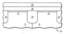
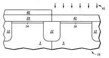
図1に、本発明の一実施例による半導体素子の構造の一部分10を示す。この半導体素子構造は、第1導電型の第1領域3,第2導電型の第2領域5,フィールド分離領域12,第1ゲート誘電体層14,および第2ゲート誘電体層16を有する半導体基板から成る。一実施例では、半導体基板は単結晶シリコン基板である。あるいは、半導体基板は、絶縁物上シリコン基板,ゲルマニウム基板,シリコン・ゲルマニウム基板,サファイア基板上シリコン等とすることも可能である。
【0007】
一実施例では、フィールド分離領域12は、トレンチ分離領域であり、従来のエッチングおよび化学機械式研摩技法を用いて形成する。あるいは、フィールド分離領域12は、シリコン選択酸化(LOCOS),ポリ・バッファLOCOS(BPL),ポリシリコン封入選択酸化(PELOX)等のような従来からの技法を用いて形成したフィールド酸化物領域とすることも可能である。一実施例では、ゲート誘電体層14およびゲート誘電体層16は、熱二酸化シリコン層であり、第1領域3の一部分および第2領域5の一部分をそれぞれ熱的に酸化させることによって形成する。あるいは、ゲート誘電体層14およびゲート誘電体層16は、窒化シリコンの層,酸窒化シリコンの層,化学蒸着した二酸化シリコンの層,窒化した酸化物層(nitrided oxide layer),金属酸化物のような高−k誘電体物質,またはその組み合わせとすることも可能である。尚、ゲート誘電体層14およびゲート誘電体層16は同時に形成可能であることは認められよう。あるいは、ゲート誘電体層14およびゲート誘電体層16は、異なる時点に、異なるゲート誘電体物質で形成することも可能である。
【0008】
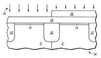
図2において、第1領域3および第2領域5上に、導電層18を形成する。一実施例では、導電層18は、タンタル,タングステン,モリブデン,ジルコニウム,ハフニウム(hafnium),バナジウム,クロム,ニオブ,チタン等のような金属層である。あるいは、導電層18は、タンタル・シリサイド,タングステン・シリサイド,モリブデン・シリサイド,チタン・シリサイド等のような、金属シリサイド層とすることも可能である。導電層18は、従来の化学蒸着技法またはスパッタリング技法を用いて形成可能である。
【0009】
図3において、導電層18上に、マスキング層20を形成する。一実施例では、マスキング層20は窒化シリコンの層であり、急速熱化学蒸着を用いて堆積する。あるいは、マスキング層20は、フォトレジストの層またはポリシリコンの層とすることも可能である。
【0010】
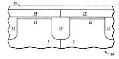
図4において、マスキング層20にパターニングを行い、導電層18の第1部分を露出させ、導電層18の第2部分の上にあるマスキング層20の残り部分を残留させる。次に、導電層18の露出部分を窒化し、第1領域3上に導電性窒化物層24を形成する。一実施例では、導電性窒化物層24を形成するには、窒素イオン22を導電層18の露出部分内に注入する。尚、マスキング層20の残り部分は、窒素イオンが導電層18の第2部分に注入されるのを防止することは認められよう。窒素注入の後、半導体素子構造をアニールし、導電性窒化物層24を形成する。半導体素子構造をアニールするには、従来のファーネス(furnace)または急速熱アニーリング・システムを用いることができる。フォトレジストを用いてマスキング層20を形成する場合、アニーリングの前にこれを除去しなければならないことは認められよう。あるいは、導電性窒化物層24は、アンモニアのような窒素雰囲気において導電層18の露出部分をアニールすることによって、または導電層18の露出部分を、窒素を含むプラズマに露出させることによって形成することも可能である。尚、導電層18がタンタル,タングステン,モリブデン,ジルコニウム,ハフニウム,バナジウム,クロム,ニオブ,またはチタンの層である場合、導電性窒化物層24は、それぞれ、窒化タンタル,窒化タングステン,窒化モリブデン,窒化ジルコニウム,窒化ハフニウム,窒化バナジウム,窒化クロム,窒化ニオブ,または窒化チタンの層となることを注記しておく。同様に、導電層18がタンタル・シリサイド,タングステン・シリサイド,モリブデン・シリサイド,またはチタン・シリサイドの層である場合、導電性窒化物層24は、それぞれ、窒化タンタル・シリコン,窒化タングステン・シリコン,窒化モリブデン・シリコン,または窒化チタン・シリコンの層となる。
【0011】
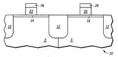
図5において、導電性窒化物層24および導電層18の残り部分の上に、キャッピング層26を形成する。一実施例では、キャッピング層26は窒化シリコンの層であり、急速熱化学蒸着を用いて堆積する。あるいは、キャッピング層26はポリシリコンの層とすることも可能であり、この場合も急速熱化学蒸着を用いて堆積する。尚、ポリシリコンを用いてキャッピング層26を形成する場合、窒化チタンのようなバリア層を、ポリシリコン層と下地の導電性窒化物層24および導電層18との間に形成し、ポリシリコン層と下地の導電性金属層18および導電性窒化物層24との間のシリサイド化を防止しなければならない場合もあることを注記しておく。また、キャッピング層26を用いて、後続処理の間、導電性窒化物層24および導電層18の残り部分の酸化を防止することは認められよう。
【0012】
図6において、導電性窒化物層24にパターニングを行い、第1領域3上に第1ゲート電極23を形成し、導電層18の残り部分にパターニングを行い、第2領域5上に第2ゲート電極25を形成する。図6に示すように、キャッピング層26の一部分を、第1ゲート電極23上および第2ゲート電極25上に残す。導電性窒化物層24および導電層18の残り部分は、従来のエッチング技法を用いて、同時にまたは別個の工程でパターニング可能であることは認められよう。
【0013】
図7において、第1ゲート電極23および第2ゲート電極25の側壁に沿って、側壁スペーサ28を形成する。一実施例では、側壁スペーサ28は、窒化シリコンの側壁スペーサであり、高速熱化学蒸着および従来のエッチング技法を用いて形成する。尚、側壁スペーサ28は、第1ゲート電極23および第2ゲート電極25が後続処理工程の間に酸化されるのを防止することは認められよう。加えて、第1領域3内に、第2導電型を有するソース・ドレイン領域30を形成し、第2領域5内に、第1導電型を有するソース・ドレイン領域34を形成し、第1領域3内に第1トランジスタ27、そして第2領域5内に第2トランジスタ29を形成する。尚、ゲート電極23は、ゲート電極25とは異なる仕事関数を有することは認められよう。例えば、第1ゲート領域3がN−型導電性を有し、第2領域5がP−型導電性を有する場合、ゲート電極23の仕事関数は、ゲート電極25の仕事関数よりも大きくなる。
【0014】
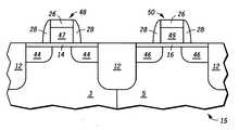
図8に、本発明の別の実施例を示す。ここでは、導電性窒化物層24を形成した後に、図4に示したマスキング層20を除去する。次に、導電層18の残り部分を露出させるように、導電性窒化物層24上に第2マスキング層40を形成する。一実施例では、マスキング層40は窒化シリコンの層であり、急速熱化学蒸着を用いて堆積する。あるいは、マスキング層40はフォトレジストの層またはポリシリコンの層とすることも可能である。マスキング層40を形成した後、次いで導電層18の残り部分を窒化して導電性窒化物層42を形成する。一実施例では、導電層18の残り部分に窒素イオン41を注入し、次いで半導体素子構造15をアニールし、導電性窒化物層42を形成する。あるいは、アンモニアのような窒素雰囲気において導電層18の残り部分をアニールすることによって、または導電層18の残り部分を、窒素を含むプラズマに露出させることによって、導電性窒化物層42を形成することも可能である。尚、導電層18がタンタル,タングステン,モリブデン,ジルコニウム,ハフニウム,バナジウム,クロム,ニオブ,またはチタンの層である場合、導電性窒化物層42は、それぞれ、窒化タンタル,窒化タングステン,窒化モリブデン,窒化ジルコニウム,窒化ハフニウム,窒化バナジウム,窒化クロム,窒化ニオブ,または窒化チタンの層となることを注記しておく。同様に、導電層18がタンタル・シリサイド,タングステン・シリサイド,モリブデン・シリサイド,またはチタン・シリサイドの層である場合、導電性窒化物層42は、それぞれ、窒化タンタル・シリコン,窒化タングステン・シリコン,窒化モリブデン・シリコン,または窒化チタン・シリコンとなる。
【0015】
図9において、マスキング層40を除去し、図5ないし図8において先に説明したように処理を続ける。これによって、第1領域3上に第1トランジスタ48が形成され、第2領域5上に第2トランジスタ50が形成される。トランジスタ48のゲート電極47は、導電性窒化物層24の一部から成り、第1仕事関数値を有すること、およびトランジスタ50のゲート電極49は導電性窒化物層42の一部から成り、第2の仕事関数値を有することが認められよう。例えば、トランジスタ48は、第1仕事関数値を有する窒化タンタルのゲート電極を有するように形成することができ、トランジスタ50は、第2の仕事関数値を有する窒化タンタルのゲート電極を有するように形成することができる。更に具体的には、第1領域3がN−型導電性を有し、第2領域5がP−型導電性を有する場合、第1トランジスタ48の窒化タンタル・ゲート電極は、トランジスタ50の窒化タンタル・ゲート電極よりも大きな仕事関数値を有するように形成する。尚、導電性窒化物の仕事関数は、窒素濃度が高くなる程、増大することを注記しておく。したがって、異なる窒素濃度を有する導電性窒化物層を形成することによって、異なる仕事関数を有するゲート電極を形成することができる。即ち、非化学量論的金属濃厚導電性窒化物(non-stoichiometric metal-rich conductive nitride)は、化学量論的導電性窒化物よりも小さな仕事関数を有する。何故なら、窒素濃度が低いからである。
【0016】
本明細書に含まれるこれまでの説明および図は、本発明に関連する利点の多くを例証するものである。即ち、素子の性能を最適化するために異なる仕事関数を有するゲート電極を利用したCMOS素子構造が開示された。
【0017】
以上の説明から、本発明によれば、先に明記した必要性を完全に満たし、利点が得られるCMOS素子が提供されたことが認められよう。本発明は、その具体的な実施例を参照しながら説明しかつ図示したが、本発明が例示の実施例に限定されることを意図する訳ではない。本発明の精神から逸脱することなく、変更や変形が可能であることを当業者は認めよう。
【図面の簡単な説明】
【図1】本発明による半導体素子を形成するために用いられる工程を示す断面図。
【図2】本発明による半導体素子を形成するために用いられる工程を示す断面図。
【図3】本発明による半導体素子を形成するために用いられる工程を示す断面図。
【図4】本発明による半導体素子を形成するために用いられる工程を示す断面図。
【図5】本発明による半導体素子を形成するために用いられる工程を示す断面図。
【図6】本発明による半導体素子を形成するために用いられる工程を示す断面図。
【図7】本発明による半導体素子を形成するために用いられる工程を示す断面図。
【図8】本発明の別の実施例による半導体素子を形成するために用いられる工程を示す断面図。
【図9】本発明の別の実施例による半導体素子を形成するために用いられる工程を示す断面図。
【符号の説明】
3 第1領域
5 第2領域
10 半導体素子構造
12 フィールド分離領域
14 第1ゲート誘電体層
15 半導体素子構造
16 第2ゲート誘電体層
18 導電層
20 マスキング層
22 窒素イオン
23 第1ゲート電極
24 導電性窒化物層
25 第2ゲート電極
26 キャッピング層
28 側壁スペーサ
30,34 ソース・ドレイン領域
40 第2マスキング層
41 窒素イオン
42 導電性窒化物層
47,49 ゲート電極
48,50 トランジスタ[0001]
BACKGROUND OF THE INVENTION
The present invention relates generally to semiconductor devices, and more particularly to complementary metal oxide semiconductor devices and their formation.
[0002]
[Prior art]
In high performance semiconductors, metal gates are being used to overcome the problems associated with polysilicon depletion. Due to the semiconducting nature of the polysilicon gate electrode, band-bending or potential wells occur in the gate. Carriers are confined within dimensions comparable to their wavelength. Depending on the charge distribution in the polysilicon layer, a finite bias-dependent nature of the gate electrode capacitance (CP ) due to the depletion effect of the polysilicon occurs. As gate oxides become thinner with scaling in complementary metal oxide semiconductor (CMOS) technology, the gate oxide capacitance (COX ) increases, resulting in device thresholds. In the gate bias range near the voltage, COX is comparable to the capacitance of the polysilicon gate electrode. This results in an overall decrease in the total gate capacitance (CG ) that is undesirable.
[0003]
This effect becomes even more severe when the semiconductor device operates in the inversion mode, and the overall capacitance reduction is about 30% when the carrier concentration in the polysilicon gate electrode is less than 1020 / cm3. May occur. Excessive doping, such as doping of a P + gate that can increase CP , makes the threshold voltage (Vt ) unstable.
[0004]
It is known that the use of a metal gate can eliminate the depletion effect of polysilicon. It is also well known that polysilicon gates have a high resistivity, so that the gate needs to be silicided to reduce the overall resistivity. Depending on the design environment, the high resistance of the polysilicon gate may be necessary if not all gates can be silicided or desirable, such as SRAM that does not silicide all parts due to the need for a metal interconnect layer. The rate is disadvantageous. In addition, when using fully depleted silicon on insulator (FDSOI) technology, the use of a polysilicon gate with a practical SOI thickness will yield the optimum Vt. Impossible. In addition, the use of polysilicon gates is inconsistent with the use of high dielectric constant (high-k) metal oxide dielectrics, where high-k values are typically greater than 3.9 And silicon from the polysilicon may react with the metal oxide, causing contamination of the metal oxide gate dielectric and affecting its high-k characteristics.
[0005]
[Problems to be solved by the invention]
In CMOS technology, N + poly and P + poly are used as gates in NMOS and PMOS devices, respectively. N + poly and P + poly correspond to a work function of 4.1 eV for the N + poly gate and 5.2 eV for the P + poly gate. With current device dimensions, silicon channel doping of 1E17 / cm3 or more is required to avoid short channel effects. When replacing with a double doped silicon gate, the work function of the metal must be selected. In one known method, when selecting a metal, it has been selected to have a mid-gap work function symmetric Vt can be obtained in both NMOS device and PMOS device (mid-gap work function) . However, due to the doping requirements needed to avoid the short channel effect, the mid-gap metal, low-voltage, low-power, resulting in too large Vt is the performance element. Therefore, it is desirable to have a method of providing low Vt in both NMOS device and PMOS device.
[0006]
DETAILED DESCRIPTION OF THE INVENTION
FIG. 1 shows a
[0007]
In one embodiment,
[0008]
In FIG. 2, a
[0009]
In FIG. 3, a
[0010]
In FIG. 4, the
[0011]
In FIG. 5, a
[0012]
In FIG. 6, the
[0013]
In FIG. 7,
[0014]
FIG. 8 shows another embodiment of the present invention. Here, after the
[0015]
In FIG. 9, the
[0016]
The foregoing description and figures contained in this specification illustrate many of the advantages associated with the present invention. That is, a CMOS device structure using gate electrodes having different work functions in order to optimize device performance has been disclosed.
[0017]
From the foregoing description, it will be appreciated that according to the present invention, a CMOS device has been provided that fully satisfies the needs specified above and provides advantages. Although the invention has been described and illustrated with reference to specific embodiments thereof, it is not intended that the invention be limited to the illustrated embodiments. Those skilled in the art will recognize that modifications and variations can be made without departing from the spirit of the invention.
[Brief description of the drawings]
1 is a cross-sectional view showing a process used to form a semiconductor device according to the present invention.
FIG. 2 is a sectional view showing a process used to form a semiconductor device according to the present invention.
FIG. 3 is a sectional view showing a process used to form a semiconductor device according to the present invention.
FIG. 4 is a cross-sectional view showing a process used to form a semiconductor device according to the present invention.
FIG. 5 is a cross-sectional view showing a process used to form a semiconductor device according to the present invention.
FIG. 6 is a cross-sectional view showing a process used to form a semiconductor device according to the present invention.
FIG. 7 is a cross-sectional view showing a process used to form a semiconductor device according to the present invention.
FIG. 8 is a cross-sectional view showing a process used to form a semiconductor device according to another embodiment of the present invention.
FIG. 9 is a cross-sectional view showing a process used to form a semiconductor device according to another embodiment of the present invention.
[Explanation of symbols]
3
Claims (8)
Translated fromJapanese半導体基板を用意する段階であって、N−型の第1領域とP−型の第2領域とを有する前記半導体基板を用意する段階;
前記半導体基板上に導電層を形成する段階であって、前記第1領域上に第1部分を有し前記第2領域上に第2部分を有する前記導電層を形成する段階;
前記導電層の前記第1部分を窒化し、前記第1領域上に導電性窒化物層を形成する段階;
前記導電性窒化物層にパターニングを行い、前記第1領域上に第1ゲート電極を形成する段階;および
前記導電層にパターニングを行い、前記第2領域上に第2ゲート電極を形成する段階;
を具備することを特徴とする方法。A method for forming a semiconductor device, comprising:
Providing a semiconductor substrate, the semiconductor substrate having an N-type first region and a P-type second region;
Forming a conductive layer on the semiconductor substrate, the conductive layer having a first portion on the first region and a second portion on the second region;
Nitriding the first portion of the conductive layer to form a conductive nitride layer on the first region;
Patterning the conductive nitride layer to form a first gate electrode on the first region; and patterning the conductive layer to form a second gate electrode on the second region;
A method comprising the steps of:
N型の第1領域およびP型の第2領域を有する半導体基板;
前記第1領域上に設けられ、第1金属窒化物層より成る第1ゲート電極であって、第1仕事関数値を有する第1ゲート電極;および
前記第2領域上に設けられ、第2金属窒化物層より成る第2ゲート電極であって、第2仕事関数値及び前記第1金属窒化物層の窒素濃度よりも低い窒素濃度を有し、前記第2仕事関数値が前記第1仕事関数値よりも小さい、第2ゲート電極;
を具備することを特徴とする半導体素子。A semiconductor device:
A semiconductor substrate having anN-type first regionand the P-type second region of;
A first gate electrodeprovided on the first region and comprising a first metal nitride layer, the first gate electrode having a first work function value; and a second metalprovided on thesecond region. A second gate electrode made of a nitride layer, having a second work function value and a nitrogen concentration lower than a nitrogen concentration of the first metal nitride layer, wherein the second work function value is the first work function. A second gate electrode less than the value;
A semiconductor device comprising:
Applications Claiming Priority (3)
| Application Number | Priority Date | Filing Date | Title |
|---|---|---|---|
| US107963 | 1998-06-30 | ||
| US09/107,963US6027961A (en) | 1998-06-30 | 1998-06-30 | CMOS semiconductor devices and method of formation |
| CN99110023ACN1122307C (en) | 1998-06-30 | 1999-06-29 | Complementary metal oxide semiconductor device and formation method thereof |
Publications (2)
| Publication Number | Publication Date |
|---|---|
| JP2000031296A JP2000031296A (en) | 2000-01-28 |
| JP4226149B2true JP4226149B2 (en) | 2009-02-18 |
Family
ID=25745029
Family Applications (1)
| Application Number | Title | Priority Date | Filing Date |
|---|---|---|---|
| JP18267399AExpired - LifetimeJP4226149B2 (en) | 1998-06-30 | 1999-06-29 | CMOS semiconductor device and method for forming the same |
Country Status (3)
| Country | Link |
|---|---|
| US (1) | US6027961A (en) |
| JP (1) | JP4226149B2 (en) |
| CN (1) | CN1122307C (en) |
Families Citing this family (153)
| Publication number | Priority date | Publication date | Assignee | Title |
|---|---|---|---|---|
| US6103609A (en)* | 1997-12-11 | 2000-08-15 | Lg Semicon Co., Ltd. | Method for fabricating semiconductor device |
| US6166417A (en)* | 1998-06-30 | 2000-12-26 | Intel Corporation | Complementary metal gates and a process for implementation |
| US20020008257A1 (en)* | 1998-09-30 | 2002-01-24 | John P. Barnak | Mosfet gate electrodes having performance tuned work functions and methods of making same |
| US6197668B1 (en)* | 1998-11-06 | 2001-03-06 | Advanced Micro Devices, Inc. | Ferroelectric-enhanced tantalum pentoxide for dielectric material applications in CMOS devices |
| JP3361068B2 (en)* | 1998-12-22 | 2003-01-07 | 株式会社東芝 | Semiconductor device and manufacturing method thereof |
| US6137145A (en)* | 1999-01-26 | 2000-10-24 | Advanced Micro Devices, Inc. | Semiconductor topography including integrated circuit gate conductors incorporating dual layers of polysilicon |
| US6291282B1 (en)* | 1999-02-26 | 2001-09-18 | Texas Instruments Incorporated | Method of forming dual metal gate structures or CMOS devices |
| US7554829B2 (en) | 1999-07-30 | 2009-06-30 | Micron Technology, Inc. | Transmission lines for CMOS integrated circuits |
| JP2001085686A (en)* | 1999-09-13 | 2001-03-30 | Mitsubishi Electric Corp | Semiconductor device and manufacturing method thereof |
| US6383879B1 (en)* | 1999-12-03 | 2002-05-07 | Agere Systems Guardian Corp. | Semiconductor device having a metal gate with a work function compatible with a semiconductor device |
| US6660664B1 (en)* | 2000-03-31 | 2003-12-09 | International Business Machines Corp. | Structure and method for formation of a blocked silicide resistor |
| JP2001298192A (en)* | 2000-04-13 | 2001-10-26 | Seiko Epson Corp | Semiconductor device and method of manufacturing the same |
| JP2001298193A (en) | 2000-04-13 | 2001-10-26 | Seiko Epson Corp | Semiconductor device and method of manufacturing the same |
| JP4761646B2 (en)* | 2000-04-27 | 2011-08-31 | 株式会社半導体エネルギー研究所 | Non-volatile memory |
| US6577531B2 (en)* | 2000-04-27 | 2003-06-10 | Semiconductor Energy Laboratory Co., Ltd. | Nonvolatile memory and semiconductor device |
| US6417037B1 (en)* | 2000-07-18 | 2002-07-09 | Chartered Semiconductor Manufacturing Ltd. | Method of dual gate process |
| JP2002217313A (en)* | 2000-11-30 | 2002-08-02 | Texas Instruments Inc | Complementary transistors having respective gates formed from metal and corresponding metal silicide |
| US20020072209A1 (en)* | 2000-12-11 | 2002-06-13 | Vanguard International Semiconductor Corporation | Method of forming tungsten nitride layer as metal diffusion barrier in gate structure of MOSFET device |
| KR100387259B1 (en)* | 2000-12-29 | 2003-06-12 | 주식회사 하이닉스반도체 | Method of manufacturing a semiconductor device |
| KR100482745B1 (en)* | 2000-12-29 | 2005-04-14 | 주식회사 하이닉스반도체 | Method of manufacturing a transistor in a semiconductor device |
| US6852167B2 (en) | 2001-03-01 | 2005-02-08 | Micron Technology, Inc. | Methods, systems, and apparatus for uniform chemical-vapor depositions |
| US6410376B1 (en) | 2001-03-02 | 2002-06-25 | Chartered Semiconductor Manufacturing Ltd. | Method to fabricate dual-metal CMOS transistors for sub-0.1 μm ULSI integration |
| DE60220230T2 (en)* | 2001-04-02 | 2007-09-13 | Matsushita Electric Industrial Co., Ltd., Kadoma | METHOD OF MANUFACTURING A SEMICONDUCTOR COMPONENT |
| KR100399356B1 (en)* | 2001-04-11 | 2003-09-26 | 삼성전자주식회사 | Method of forming cmos type semiconductor device having dual gate |
| US6764912B1 (en) | 2001-08-02 | 2004-07-20 | Advanced Micro Devices, Inc. | Passivation of nitride spacer |
| US6784506B2 (en) | 2001-08-28 | 2004-08-31 | Advanced Micro Devices, Inc. | Silicide process using high K-dielectrics |
| US8026161B2 (en)* | 2001-08-30 | 2011-09-27 | Micron Technology, Inc. | Highly reliable amorphous high-K gate oxide ZrO2 |
| US6844203B2 (en)* | 2001-08-30 | 2005-01-18 | Micron Technology, Inc. | Gate oxides, and methods of forming |
| US6794252B2 (en)* | 2001-09-28 | 2004-09-21 | Texas Instruments Incorporated | Method and system for forming dual work function gate electrodes in a semiconductor device |
| US6458695B1 (en)* | 2001-10-18 | 2002-10-01 | Chartered Semiconductor Manufacturing Ltd. | Methods to form dual metal gates by incorporating metals and their conductive oxides |
| US6555915B1 (en)* | 2001-10-22 | 2003-04-29 | Motorola, Inc. | Integrated circuit having interconnect to a substrate and method therefor |
| KR100400323B1 (en)* | 2001-11-01 | 2003-10-01 | 주식회사 하이닉스반도체 | CMOS of semiconductor device and method for manufacturing the same |
| US6495422B1 (en)* | 2001-11-09 | 2002-12-17 | Taiwan Semiconductor Manfacturing Company | Methods of forming high-k gate dielectrics and I/O gate oxides for advanced logic application |
| US6858908B2 (en)* | 2001-11-30 | 2005-02-22 | Texas Instruments Incorporated | Complementary transistors having respective gates formed from a metal and a corresponding metal-silicide |
| US6900122B2 (en) | 2001-12-20 | 2005-05-31 | Micron Technology, Inc. | Low-temperature grown high-quality ultra-thin praseodymium gate dielectrics |
| US6953730B2 (en)* | 2001-12-20 | 2005-10-11 | Micron Technology, Inc. | Low-temperature grown high quality ultra-thin CoTiO3 gate dielectrics |
| US6767795B2 (en)* | 2002-01-17 | 2004-07-27 | Micron Technology, Inc. | Highly reliable amorphous high-k gate dielectric ZrOXNY |
| US6664153B2 (en)* | 2002-02-08 | 2003-12-16 | Chartered Semiconductor Manufacturing Ltd. | Method to fabricate a single gate with dual work-functions |
| US6660577B2 (en)* | 2002-02-23 | 2003-12-09 | Taiwan Semiconductor Manufacturing Co. Ltd | Method for fabricating metal gates in deep sub-micron devices |
| US6812100B2 (en) | 2002-03-13 | 2004-11-02 | Micron Technology, Inc. | Evaporation of Y-Si-O films for medium-k dielectrics |
| JP2003273350A (en)* | 2002-03-15 | 2003-09-26 | Nec Corp | Semiconductor device and manufacturing method thereof |
| US7160577B2 (en)* | 2002-05-02 | 2007-01-09 | Micron Technology, Inc. | Methods for atomic-layer deposition of aluminum oxides in integrated circuits |
| US7589029B2 (en)* | 2002-05-02 | 2009-09-15 | Micron Technology, Inc. | Atomic layer deposition and conversion |
| US7045430B2 (en)* | 2002-05-02 | 2006-05-16 | Micron Technology Inc. | Atomic layer-deposited LaAlO3 films for gate dielectrics |
| US7135421B2 (en)* | 2002-06-05 | 2006-11-14 | Micron Technology, Inc. | Atomic layer-deposited hafnium aluminum oxide |
| US7205218B2 (en)* | 2002-06-05 | 2007-04-17 | Micron Technology, Inc. | Method including forming gate dielectrics having multiple lanthanide oxide layers |
| US7067439B2 (en)* | 2002-06-14 | 2006-06-27 | Applied Materials, Inc. | ALD metal oxide deposition process using direct oxidation |
| US7193893B2 (en) | 2002-06-21 | 2007-03-20 | Micron Technology, Inc. | Write once read only memory employing floating gates |
| US7154140B2 (en)* | 2002-06-21 | 2006-12-26 | Micron Technology, Inc. | Write once read only memory with large work function floating gates |
| US6804136B2 (en)* | 2002-06-21 | 2004-10-12 | Micron Technology, Inc. | Write once read only memory employing charge trapping in insulators |
| KR100476926B1 (en)* | 2002-07-02 | 2005-03-17 | 삼성전자주식회사 | Method for forming dual gate of semiconductor device |
| US7847344B2 (en) | 2002-07-08 | 2010-12-07 | Micron Technology, Inc. | Memory utilizing oxide-nitride nanolaminates |
| US7221017B2 (en)* | 2002-07-08 | 2007-05-22 | Micron Technology, Inc. | Memory utilizing oxide-conductor nanolaminates |
| US7221586B2 (en) | 2002-07-08 | 2007-05-22 | Micron Technology, Inc. | Memory utilizing oxide nanolaminates |
| US6921702B2 (en) | 2002-07-30 | 2005-07-26 | Micron Technology Inc. | Atomic layer deposited nanolaminates of HfO2/ZrO2 films as gate dielectrics |
| US6884739B2 (en) | 2002-08-15 | 2005-04-26 | Micron Technology Inc. | Lanthanide doped TiOx dielectric films by plasma oxidation |
| US6790791B2 (en)* | 2002-08-15 | 2004-09-14 | Micron Technology, Inc. | Lanthanide doped TiOx dielectric films |
| US20040036129A1 (en)* | 2002-08-22 | 2004-02-26 | Micron Technology, Inc. | Atomic layer deposition of CMOS gates with variable work functions |
| US6891233B2 (en)* | 2002-08-26 | 2005-05-10 | Chartered Semiconductor Manufacturing Ltd. | Methods to form dual metal gates by incorporating metals and their conductive oxides |
| US6967154B2 (en) | 2002-08-26 | 2005-11-22 | Micron Technology, Inc. | Enhanced atomic layer deposition |
| US7199023B2 (en)* | 2002-08-28 | 2007-04-03 | Micron Technology, Inc. | Atomic layer deposited HfSiON dielectric films wherein each precursor is independendently pulsed |
| JP4004040B2 (en)* | 2002-09-05 | 2007-11-07 | 株式会社東芝 | Semiconductor device |
| US6958302B2 (en)* | 2002-12-04 | 2005-10-25 | Micron Technology, Inc. | Atomic layer deposited Zr-Sn-Ti-O films using TiI4 |
| US7101813B2 (en)* | 2002-12-04 | 2006-09-05 | Micron Technology Inc. | Atomic layer deposited Zr-Sn-Ti-O films |
| US6869850B1 (en)* | 2002-12-20 | 2005-03-22 | Cypress Semiconductor Corporation | Self-aligned contact structure with raised source and drain |
| US6841441B2 (en)* | 2003-01-08 | 2005-01-11 | Chartered Semiconductor Manufacturing Ltd. | Method to produce dual gates (one metal and one poly or metal silicide) for CMOS devices using sputtered metal deposition, metallic ion implantation, or silicon implantation, and laser annealing |
| KR20050094474A (en)* | 2003-02-03 | 2005-09-27 | 코닌클리즈케 필립스 일렉트로닉스 엔.브이. | Method of manufacturing a semiconductor device with mos transistors comprising gate electrodes formed in a packet of metal layers deposited upon one another |
| US7192892B2 (en) | 2003-03-04 | 2007-03-20 | Micron Technology, Inc. | Atomic layer deposited dielectric layers |
| US7135369B2 (en)* | 2003-03-31 | 2006-11-14 | Micron Technology, Inc. | Atomic layer deposited ZrAlxOy dielectric layers including Zr4AlO9 |
| US7183186B2 (en)* | 2003-04-22 | 2007-02-27 | Micro Technology, Inc. | Atomic layer deposited ZrTiO4 films |
| US6828181B2 (en)* | 2003-05-08 | 2004-12-07 | International Business Machines Corporation | Dual gate material process for CMOS technologies |
| US6864141B1 (en)* | 2003-06-03 | 2005-03-08 | Lsi Logic Corporation | Method of incorporating nitrogen into metal silicate based dielectrics by energized nitrogen ion beams |
| US20040256679A1 (en)* | 2003-06-17 | 2004-12-23 | Hu Yongjun J. | Dual work function metal gates and method of forming |
| US7220665B2 (en)* | 2003-08-05 | 2007-05-22 | Micron Technology, Inc. | H2 plasma treatment |
| JP3790237B2 (en)* | 2003-08-26 | 2006-06-28 | 株式会社東芝 | Manufacturing method of semiconductor device |
| JP4143505B2 (en)* | 2003-09-03 | 2008-09-03 | 株式会社半導体理工学研究センター | MOS type semiconductor device and manufacturing method thereof |
| US6872613B1 (en)* | 2003-09-04 | 2005-03-29 | Advanced Micro Devices, Inc. | Method for integrating metals having different work functions to form CMOS gates having a high-k gate dielectric and related structure |
| US7737359B2 (en)* | 2003-09-05 | 2010-06-15 | Newire Inc. | Electrical wire and method of fabricating the electrical wire |
| US7145073B2 (en)* | 2003-09-05 | 2006-12-05 | Southwire Company | Electrical wire and method of fabricating the electrical wire |
| US7217884B2 (en) | 2004-03-02 | 2007-05-15 | Southwire Company | Electrical wire and method of fabricating the electrical wire |
| US20050095763A1 (en)* | 2003-10-29 | 2005-05-05 | Samavedam Srikanth B. | Method of forming an NMOS transistor and structure thereof |
| US6974764B2 (en)* | 2003-11-06 | 2005-12-13 | Intel Corporation | Method for making a semiconductor device having a metal gate electrode |
| US7183221B2 (en)* | 2003-11-06 | 2007-02-27 | Texas Instruments Incorporated | Method of fabricating a semiconductor having dual gate electrodes using a composition-altered metal layer |
| US7952118B2 (en)* | 2003-11-12 | 2011-05-31 | Samsung Electronics Co., Ltd. | Semiconductor device having different metal gate structures |
| US7064050B2 (en)* | 2003-11-28 | 2006-06-20 | International Business Machines Corporation | Metal carbide gate structure and method of fabrication |
| JP2005183783A (en)* | 2003-12-22 | 2005-07-07 | Seiko Epson Corp | Manufacturing method of semiconductor device |
| JP2005217176A (en)* | 2004-01-29 | 2005-08-11 | Tokyo Electron Ltd | Semiconductor device and method for forming laminated film |
| JP2005217309A (en)* | 2004-01-30 | 2005-08-11 | Toshiba Corp | Semiconductor device and manufacturing method thereof |
| US7018887B1 (en)* | 2004-03-01 | 2006-03-28 | Advanced Micro Devices, Inc. | Dual metal CMOS transistors with silicon-metal-silicon stacked gate electrode |
| US20050233477A1 (en)* | 2004-03-05 | 2005-10-20 | Tokyo Electron Limited | Substrate processing apparatus, substrate processing method, and program for implementing the method |
| US6921691B1 (en)* | 2004-03-18 | 2005-07-26 | Infineon Technologies Ag | Transistor with dopant-bearing metal in source and drain |
| US7323377B1 (en) | 2004-03-26 | 2008-01-29 | Cypress Semiconductor Corporation | Increasing self-aligned contact areas in integrated circuits using a disposable spacer |
| US7030001B2 (en)* | 2004-04-19 | 2006-04-18 | Freescale Semiconductor, Inc. | Method for forming a gate electrode having a metal |
| US8119210B2 (en)* | 2004-05-21 | 2012-02-21 | Applied Materials, Inc. | Formation of a silicon oxynitride layer on a high-k dielectric material |
| US8399934B2 (en) | 2004-12-20 | 2013-03-19 | Infineon Technologies Ag | Transistor device |
| US7592678B2 (en)* | 2004-06-17 | 2009-09-22 | Infineon Technologies Ag | CMOS transistors with dual high-k gate dielectric and methods of manufacture thereof |
| US8178902B2 (en) | 2004-06-17 | 2012-05-15 | Infineon Technologies Ag | CMOS transistor with dual high-k gate dielectric and method of manufacture thereof |
| US7439113B2 (en)* | 2004-07-12 | 2008-10-21 | Intel Corporation | Forming dual metal complementary metal oxide semiconductor integrated circuits |
| JP2006041339A (en)* | 2004-07-29 | 2006-02-09 | Fujitsu Ltd | CMOS integrated circuit |
| US7081421B2 (en) | 2004-08-26 | 2006-07-25 | Micron Technology, Inc. | Lanthanide oxide dielectric layer |
| US7494939B2 (en)* | 2004-08-31 | 2009-02-24 | Micron Technology, Inc. | Methods for forming a lanthanum-metal oxide dielectric layer |
| US7588988B2 (en) | 2004-08-31 | 2009-09-15 | Micron Technology, Inc. | Method of forming apparatus having oxide films formed using atomic layer deposition |
| JP2006108602A (en)* | 2004-09-10 | 2006-04-20 | Toshiba Corp | Semiconductor device and manufacturing method thereof |
| KR100655751B1 (en)* | 2004-10-01 | 2006-12-11 | 삼성전자주식회사 | Manufacturing Method of Semiconductor Device |
| US7344934B2 (en)* | 2004-12-06 | 2008-03-18 | Infineon Technologies Ag | CMOS transistor and method of manufacture thereof |
| US7235501B2 (en) | 2004-12-13 | 2007-06-26 | Micron Technology, Inc. | Lanthanum hafnium oxide dielectrics |
| US7253050B2 (en)* | 2004-12-20 | 2007-08-07 | Infineon Technologies Ag | Transistor device and method of manufacture thereof |
| US7402472B2 (en)* | 2005-02-25 | 2008-07-22 | Freescale Semiconductor, Inc. | Method of making a nitrided gate dielectric |
| US7332388B2 (en)* | 2005-03-08 | 2008-02-19 | Micron Technology, Inc. | Method to simultaneously form both fully silicided and partially silicided dual work function transistor gates during the manufacture of a semiconductor device, semiconductor devices, and systems including same |
| JP2006295123A (en)* | 2005-03-18 | 2006-10-26 | Fujitsu Ltd | MOS field effect semiconductor device manufacturing method and MOS field effect semiconductor device |
| US7160781B2 (en)* | 2005-03-21 | 2007-01-09 | Infineon Technologies Ag | Transistor device and methods of manufacture thereof |
| JP4982958B2 (en) | 2005-03-24 | 2012-07-25 | 富士通セミコンダクター株式会社 | Semiconductor device and manufacturing method thereof |
| US7687409B2 (en) | 2005-03-29 | 2010-03-30 | Micron Technology, Inc. | Atomic layer deposited titanium silicon oxide films |
| JP4607645B2 (en)* | 2005-04-04 | 2011-01-05 | 株式会社東芝 | Semiconductor device and manufacturing method thereof |
| JP2006294894A (en)* | 2005-04-12 | 2006-10-26 | Sony Corp | Semiconductor apparatus and its manufacturing method |
| US7361538B2 (en)* | 2005-04-14 | 2008-04-22 | Infineon Technologies Ag | Transistors and methods of manufacture thereof |
| US7662729B2 (en)* | 2005-04-28 | 2010-02-16 | Micron Technology, Inc. | Atomic layer deposition of a ruthenium layer to a lanthanide oxide dielectric layer |
| US7927948B2 (en) | 2005-07-20 | 2011-04-19 | Micron Technology, Inc. | Devices with nanocrystals and methods of formation |
| US20070052036A1 (en)* | 2005-09-02 | 2007-03-08 | Hongfa Luan | Transistors and methods of manufacture thereof |
| US8188551B2 (en) | 2005-09-30 | 2012-05-29 | Infineon Technologies Ag | Semiconductor devices and methods of manufacture thereof |
| US20070052037A1 (en)* | 2005-09-02 | 2007-03-08 | Hongfa Luan | Semiconductor devices and methods of manufacture thereof |
| US7462538B2 (en)* | 2005-11-15 | 2008-12-09 | Infineon Technologies Ag | Methods of manufacturing multiple gate CMOS transistors having different gate dielectric materials |
| WO2007069299A1 (en) | 2005-12-13 | 2007-06-21 | Fujitsu Limited | Method of manufacturing semiconductor device |
| US7495290B2 (en)* | 2005-12-14 | 2009-02-24 | Infineon Technologies Ag | Semiconductor devices and methods of manufacture thereof |
| US7510943B2 (en)* | 2005-12-16 | 2009-03-31 | Infineon Technologies Ag | Semiconductor devices and methods of manufacture thereof |
| KR100660909B1 (en)* | 2006-01-06 | 2006-12-26 | 삼성전자주식회사 | Semiconductor device and manufacturing method thereof |
| US7709402B2 (en)* | 2006-02-16 | 2010-05-04 | Micron Technology, Inc. | Conductive layers for hafnium silicon oxynitride films |
| US7678710B2 (en)* | 2006-03-09 | 2010-03-16 | Applied Materials, Inc. | Method and apparatus for fabricating a high dielectric constant transistor gate using a low energy plasma system |
| US7645710B2 (en)* | 2006-03-09 | 2010-01-12 | Applied Materials, Inc. | Method and apparatus for fabricating a high dielectric constant transistor gate using a low energy plasma system |
| US7837838B2 (en)* | 2006-03-09 | 2010-11-23 | Applied Materials, Inc. | Method of fabricating a high dielectric constant transistor gate using a low energy plasma apparatus |
| JP4828982B2 (en)* | 2006-03-28 | 2011-11-30 | 富士通セミコンダクター株式会社 | Manufacturing method of semiconductor device |
| US20070259111A1 (en)* | 2006-05-05 | 2007-11-08 | Singh Kaushal K | Method and apparatus for photo-excitation of chemicals for atomic layer deposition of dielectric film |
| KR100753558B1 (en)* | 2006-08-21 | 2007-08-30 | 삼성전자주식회사 | CMOS transistor and its manufacturing method |
| US20080050898A1 (en)* | 2006-08-23 | 2008-02-28 | Hongfa Luan | Semiconductor devices and methods of manufacture thereof |
| US7563730B2 (en) | 2006-08-31 | 2009-07-21 | Micron Technology, Inc. | Hafnium lanthanide oxynitride films |
| JP5177980B2 (en)* | 2006-09-05 | 2013-04-10 | 東京エレクトロン株式会社 | Semiconductor device and manufacturing method thereof |
| US7700470B2 (en)* | 2006-09-22 | 2010-04-20 | Intel Corporation | Selective anisotropic wet etching of workfunction metal for semiconductor devices |
| US7902018B2 (en)* | 2006-09-26 | 2011-03-08 | Applied Materials, Inc. | Fluorine plasma treatment of high-k gate stack for defect passivation |
| US8039339B2 (en)* | 2007-04-23 | 2011-10-18 | Freescale Semiconductor, Inc. | Separate layer formation in a semiconductor device |
| JP5104373B2 (en)* | 2008-02-14 | 2012-12-19 | 日本ゼオン株式会社 | Production method of retardation plate |
| US20090286387A1 (en)* | 2008-05-16 | 2009-11-19 | Gilmer David C | Modulation of Tantalum-Based Electrode Workfunction |
| US20100025778A1 (en)* | 2008-07-31 | 2010-02-04 | Chao-Sung Lai | Transistor structure and method of making the same |
| US8524588B2 (en) | 2008-08-18 | 2013-09-03 | Taiwan Semiconductor Manufacturing Company, Ltd. | Method of forming a single metal that performs N work function and P work function in a high-k/metal gate process |
| US7824986B2 (en)* | 2008-11-05 | 2010-11-02 | Micron Technology, Inc. | Methods of forming a plurality of transistor gates, and methods of forming a plurality of transistor gates having at least two different work functions |
| US9136180B2 (en)* | 2011-06-01 | 2015-09-15 | Asm Ip Holding B.V. | Process for depositing electrode with high effective work function |
| TWI613822B (en) | 2011-09-29 | 2018-02-01 | 半導體能源研究所股份有限公司 | Semiconductor device and method of manufacturing same |
| JP5390654B2 (en)* | 2012-03-08 | 2014-01-15 | 株式会社東芝 | Manufacturing method of semiconductor device |
| US8772114B2 (en)* | 2012-03-30 | 2014-07-08 | Taiwan Semiconductor Manufacturing Company, Ltd. | Metal gate semiconductor device and method of fabricating thereof |
| KR102089682B1 (en)* | 2013-07-15 | 2020-03-16 | 삼성전자 주식회사 | Semiconductor device and method for fabricating the same |
| JP6153507B2 (en)* | 2014-11-25 | 2017-06-28 | ユニサンティス エレクトロニクス シンガポール プライベート リミテッドUnisantis Electronics Singapore Pte Ltd. | Semiconductor device and manufacturing method of semiconductor device |
| JP6538604B2 (en)* | 2016-03-30 | 2019-07-03 | 株式会社Kokusai Electric | Semiconductor device manufacturing method and substrate processing apparatus |
| US10090169B1 (en)* | 2017-03-31 | 2018-10-02 | Globalfoundries Inc. | Methods of forming integrated circuit structures including opening filled with insulator in metal gate |
| US12015066B2 (en) | 2020-06-17 | 2024-06-18 | Taiwan Semiconductor Manufacturing Co., Ltd. | Triple layer high-k gate dielectric stack for workfunction engineering |
Family Cites Families (5)
| Publication number | Priority date | Publication date | Assignee | Title |
|---|---|---|---|---|
| US4605947A (en)* | 1983-03-07 | 1986-08-12 | Motorola Inc. | Titanium nitride MOS device gate electrode and method of producing |
| US5268590A (en)* | 1989-12-27 | 1993-12-07 | Motorola, Inc. | CMOS device and process |
| US5457580A (en)* | 1992-08-02 | 1995-10-10 | Goldstar Co., Ltd. | Video compression/expansion apparatus for digital VCR |
| US5416043A (en)* | 1993-07-12 | 1995-05-16 | Peregrine Semiconductor Corporation | Minimum charge FET fabricated on an ultrathin silicon on sapphire wafer |
| US5923999A (en)* | 1996-10-29 | 1999-07-13 | International Business Machines Corporation | Method of controlling dopant diffusion and metal contamination in thin polycide gate conductor of mosfet device |
- 1998
- 1998-06-30USUS09/107,963patent/US6027961A/ennot_activeExpired - Lifetime
- 1999
- 1999-06-29CNCN99110023Apatent/CN1122307C/ennot_activeExpired - Lifetime
- 1999-06-29JPJP18267399Apatent/JP4226149B2/ennot_activeExpired - Lifetime
Also Published As
| Publication number | Publication date |
|---|---|
| CN1122307C (en) | 2003-09-24 |
| JP2000031296A (en) | 2000-01-28 |
| US6027961A (en) | 2000-02-22 |
| CN1243336A (en) | 2000-02-02 |
Similar Documents
| Publication | Publication Date | Title |
|---|---|---|
| JP4226149B2 (en) | CMOS semiconductor device and method for forming the same | |
| US6727130B2 (en) | Method of forming a CMOS type semiconductor device having dual gates | |
| US7022559B2 (en) | MOSFET gate electrodes having performance tuned work functions and methods of making same | |
| EP1872407B1 (en) | Using metal/metal nitride bilayers as gate electrodes in self-aligned aggressively scaled cmos devices | |
| US8154025B2 (en) | Schottky barrier CMOS device and method | |
| US6900481B2 (en) | Non-silicon semiconductor and high-k gate dielectric metal oxide semiconductor field effect transistors | |
| US7629212B2 (en) | Doped WGe to form dual metal gates | |
| US20070026590A1 (en) | Dynamic Schottky barrier MOSFET device and method of manufacture | |
| US20070194353A1 (en) | Metal source/drain Schottky barrier silicon-on-nothing MOSFET device and method thereof | |
| US6864163B1 (en) | Fabrication of dual work-function metal gate structure for complementary field effect transistors | |
| US20080050898A1 (en) | Semiconductor devices and methods of manufacture thereof | |
| US7429770B2 (en) | Semiconductor device and manufacturing method thereof | |
| US20080093666A1 (en) | Semiconductor Device and Manufacturing Method Thereof | |
| US6762468B2 (en) | Semiconductor device and method of manufacturing the same | |
| JP2004247341A (en) | Semiconductor device | |
| JP4011014B2 (en) | Semiconductor device and manufacturing method thereof | |
| TW459351B (en) | CMOS semiconductor devices and method of formation | |
| JP2658238B2 (en) | Semiconductor device | |
| JPH01189954A (en) | Manufacture of complementary type semiconductor device and semiconductor device | |
| JPH0766295A (en) | Semiconductor device | |
| JPH0645595A (en) | Buried channel-type p-channel misfet |
Legal Events
| Date | Code | Title | Description |
|---|---|---|---|
| A711 | Notification of change in applicant | Free format text:JAPANESE INTERMEDIATE CODE: A711 Effective date:20041217 | |
| RD02 | Notification of acceptance of power of attorney | Free format text:JAPANESE INTERMEDIATE CODE: A7422 Effective date:20051216 | |
| A621 | Written request for application examination | Free format text:JAPANESE INTERMEDIATE CODE: A621 Effective date:20060628 | |
| A977 | Report on retrieval | Free format text:JAPANESE INTERMEDIATE CODE: A971007 Effective date:20071005 | |
| A131 | Notification of reasons for refusal | Free format text:JAPANESE INTERMEDIATE CODE: A131 Effective date:20071023 | |
| A521 | Request for written amendment filed | Free format text:JAPANESE INTERMEDIATE CODE: A523 Effective date:20080117 | |
| A131 | Notification of reasons for refusal | Free format text:JAPANESE INTERMEDIATE CODE: A131 Effective date:20080401 | |
| A601 | Written request for extension of time | Free format text:JAPANESE INTERMEDIATE CODE: A601 Effective date:20080701 | |
| A602 | Written permission of extension of time | Free format text:JAPANESE INTERMEDIATE CODE: A602 Effective date:20080704 | |
| A601 | Written request for extension of time | Free format text:JAPANESE INTERMEDIATE CODE: A601 Effective date:20080801 | |
| A602 | Written permission of extension of time | Free format text:JAPANESE INTERMEDIATE CODE: A602 Effective date:20080807 | |
| A601 | Written request for extension of time | Free format text:JAPANESE INTERMEDIATE CODE: A601 Effective date:20080901 | |
| A602 | Written permission of extension of time | Free format text:JAPANESE INTERMEDIATE CODE: A602 Effective date:20080905 | |
| RD04 | Notification of resignation of power of attorney | Free format text:JAPANESE INTERMEDIATE CODE: A7424 Effective date:20080922 | |
| A521 | Request for written amendment filed | Free format text:JAPANESE INTERMEDIATE CODE: A523 Effective date:20080929 | |
| TRDD | Decision of grant or rejection written | ||
| A01 | Written decision to grant a patent or to grant a registration (utility model) | Free format text:JAPANESE INTERMEDIATE CODE: A01 Effective date:20081118 | |
| A01 | Written decision to grant a patent or to grant a registration (utility model) | Free format text:JAPANESE INTERMEDIATE CODE: A01 | |
| A61 | First payment of annual fees (during grant procedure) | Free format text:JAPANESE INTERMEDIATE CODE: A61 Effective date:20081126 | |
| FPAY | Renewal fee payment (event date is renewal date of database) | Free format text:PAYMENT UNTIL: 20111205 Year of fee payment:3 | |
| R150 | Certificate of patent or registration of utility model | Free format text:JAPANESE INTERMEDIATE CODE: R150 Ref document number:4226149 Country of ref document:JP Free format text:JAPANESE INTERMEDIATE CODE: R150 | |
| FPAY | Renewal fee payment (event date is renewal date of database) | Free format text:PAYMENT UNTIL: 20111205 Year of fee payment:3 | |
| FPAY | Renewal fee payment (event date is renewal date of database) | Free format text:PAYMENT UNTIL: 20121205 Year of fee payment:4 | |
| R250 | Receipt of annual fees | Free format text:JAPANESE INTERMEDIATE CODE: R250 | |
| FPAY | Renewal fee payment (event date is renewal date of database) | Free format text:PAYMENT UNTIL: 20131205 Year of fee payment:5 | |
| R250 | Receipt of annual fees | Free format text:JAPANESE INTERMEDIATE CODE: R250 | |
| R250 | Receipt of annual fees | Free format text:JAPANESE INTERMEDIATE CODE: R250 | |
| R250 | Receipt of annual fees | Free format text:JAPANESE INTERMEDIATE CODE: R250 | |
| R250 | Receipt of annual fees | Free format text:JAPANESE INTERMEDIATE CODE: R250 | |
| R250 | Receipt of annual fees | Free format text:JAPANESE INTERMEDIATE CODE: R250 | |
| S533 | Written request for registration of change of name | Free format text:JAPANESE INTERMEDIATE CODE: R313533 | |
| R350 | Written notification of registration of transfer | Free format text:JAPANESE INTERMEDIATE CODE: R350 | |
| R250 | Receipt of annual fees | Free format text:JAPANESE INTERMEDIATE CODE: R250 | |
| R250 | Receipt of annual fees | Free format text:JAPANESE INTERMEDIATE CODE: R250 | |
| EXPY | Cancellation because of completion of term |