JP4225811B2 - IC card and IC card system - Google Patents
IC card and IC card systemDownload PDFInfo
- Publication number
- JP4225811B2 JP4225811B2JP2003078388AJP2003078388AJP4225811B2JP 4225811 B2JP4225811 B2JP 4225811B2JP 2003078388 AJP2003078388 AJP 2003078388AJP 2003078388 AJP2003078388 AJP 2003078388AJP 4225811 B2JP4225811 B2JP 4225811B2
- Authority
- JP
- Japan
- Prior art keywords
- card
- antenna coil
- folded
- communication
- state
- Prior art date
- Legal status (The legal status is an assumption and is not a legal conclusion. Google has not performed a legal analysis and makes no representation as to the accuracy of the status listed.)
- Expired - Fee Related
Links
Images


Landscapes
- Details Of Aerials (AREA)
- Support Of Aerials (AREA)
Description
Translated fromJapanese【0001】
【発明の属する技術分野】
本発明は、カード本体にICチップとアンテナコイルを搭載し、リーダライタと非接触で通信を行うICカード及び当該ICカードにリーダライタを備えたICカードシステムに関するものである。
【0002】
【従来の技術】
特開2000−306066号公報に、ICカード上にスイッチを設け、このスイッチのオン/オフにより、ICカード上のICチップにアンテナコイルを接続、解放するというICカードが開示されている。
【0003】
【発明が解決しようとする課題】
しかしながら、上述した従来の方式の場合、機械式接点によるスイッチが必要とあるが、カード等の薄い(0.1mm〜数ミリ程度)ものの中にスイッチを入れるのは困難である。また、接触部分があるため、抵抗値を持ったり、腐食等による接点の劣化も心配され、信頼性に乏しい。
【0004】
本発明は上述した点に鑑みてなされたもので、機械式接点によるスイッチを用いることがなく、また、通信周波数を容易に変えることができるICカード及びICカードシステムを提供することを目的とする。
【0005】
【課題を解決するための手段】
本発明に係るICカードは、カード本体にICチップとアンテナコイルを搭載し、リーダライタと非接触で通信を行うICカードにおいて、前記カード本体をカード面上の予め定めた任意の位置を起点として折り畳み可能に構成し、前記アンテナコイルのインダクタンスを、カード本体を折り畳んだ状態と折り畳まない状態とで変化させることで、異なる通信周波数を得ることを特徴とするものである。この構成によれば、カード本体の折り畳み状態と非折り畳み状態とで異なる通信周波数を得ることができ、折り畳み状態を送受信可能にし、非折り畳み状態を送受信不可能にすることで、機械式接点によるスイッチを不要にすることができる。
【0006】
また、前記アンテナコイルは、8の字状に形成され、該8の字の交点付近を前記予め定めた任意の位置の起点とすることを特徴とするものである。この構成によれば、異なる通信周波数を得ることを特徴とするものである。この構成によれば、カード本体の折り畳み状態と非折り畳み状態とで異なる通信周波数を得ることができ、折り畳み状態を送受信可能にし、非折り畳み状態を送受信不可能にすることで、機械式接点によるスイッチを不要にすることができる。
【0007】
また、前記アンテナコイルの8の字の一方のループと他方のループとは、異なる面積を有することを特徴とするものである。この構成によれば、ループ面積が異なることによる2周波通信を可能にすることができる。
【0008】
また、前記カード本体を折り曲げた状態での通信可能な前記アンテナコイルの有効面積は、折り曲げない状態での前記アンテナコイルの有効面積の1/2より小さいことを特徴とするものである。この構成によれば、5MHz帯の通信周波数と13MHz帯の通信周波数の2つのICカードの規格を得ることができる。
【0009】
また、前記ICチップとして、前記カード本体を折り曲げた状態での通信周波数に対応するICチップと、折り曲げない状態での通信周波数に対応するICチップとの2つのICチップを搭載することを特徴とするものである。この構成によれば、5MHz帯用のICチップと13MHz帯用のICチップの2つのICカードの規格を満たすICチップを搭載することができる。
【0010】
また、前記カード本体の表面と裏面に文字が印字され、前記カード本体を折り曲げると、非折り曲げ時と異なる文字列を表記することを特徴とするものである。この構成によれば、カード本体の折り曲げ時と非折り曲げ時の通信周波数の区別の表記を行うことができる。
【0011】
さらに、本発明に係るICカードシステムは、前記記載のICカードと、当該ICカードと非接触で通信を行うリーダライタとを備えたICカードシステムにおいて、前記リーダライタは、予め定められた任意の通信周波数でデータを送信し、前記ICカードが折り曲げ状態または非折り曲げ状態で前記データを受信する場合、前記予め定められた任意の通信周波数が前記ICカードの折り曲げ状態または非折り曲げ状態に基づく通信周波数と合致していない場合は、当該ICカードを現状の状態とは異なる状態に変更するように指示を出力することを特徴とするものである。この構成によれば、2周波通信時にリーダライタに定められた通信周波数に合致させて通信を行うことができる。
【0012】
【発明の実施の形態】
実施の形態1
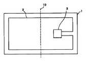
図1は、一般的な非接触ICカードの構造を示した図である。図1に示すように、ICカード1にはアンテナコイル2とICチップ3が搭載されており、アンテナコイル2は1ターンしか巻いていないが、数ターンでも良い。
【0013】
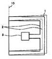
図2は、本発明の実施の形態1によるICカードの構造を示した図である。図2に示すように、本実施の形態に係るICカード1は、その内部にアンテナコイル2とICチップ3が設けられると共に、カード面上の予め定められた任意の位置を起点としてカード本体1を左側と右側に等分割する中心線を折り畳み線10とし、この折り畳み線10に沿って折り畳み可能に構成されており、折り畳み線10で示されるICカード10の中央部分でカードを2つに折り畳むことができるようになっている。
【0014】
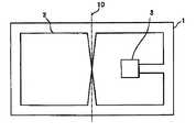
図3は、図2に示すICカード1を折り畳み線10で2つに折曲げたところを示した図である。このICカード1は、広げている場合には1個のアンテナコイル2が存在し、所定の通信周波数で通信可能であるが、折り畳み線10で2つに折った場合、左右のコイル2のパターンが重なり合い、コイルの開口部の面積が小さくなる。コイル2のインダクタンスは、この開口部の面積に比例して大きくなるため、この場合はインダクタンスが小さくなる。完全にコイルが重なった場合には、理論上、インダクタンスは0となる。このため、アンテナコイル2が交流磁界より受ける信号は小さくなり、ICチップ3を働かなくすることができ、通信不可(通信周波数=0)となる。
【0015】
図4は、ICチップ3の部分に共振用コンデンサを取付けた図である。図4に示すように、ICチップ3の部分に共振用コンデンサ4を取付け、共振コンデンサ4の値を調節し、交流磁界の周波数で共振させた場合、先鋭度(Q)倍の電圧がアンテナコイル2に発生し、ICカード1により多くの電圧を与えることができる。尚、このコンデンサ4は、ICチップ3の入力容量や、ICカード10上のコイルの浮遊容量等で同じ効果を得ることができる。
【0016】
図5は、図4のカードを折り畳み線10に沿って二つ折りにした場合を示す図で、このカードの場合、インダクタンスはゼロに近くなり、共振コンデンサ4があってもほとんど電圧が発生しなくなり、ICチップ3は動作しなくなる。
【0017】
従って、上記実施の形態1によれば、カード本体をカード面上の予め定めた任意の位置を起点として折り畳み可能に構成し、アンテナコイルのインダクタンスを、カード本体を折り畳んだ状態と折り畳まない状態とで変化させることで、カード本体の折り畳み状態と非折り畳み状態とで異なる通信周波数を得ることができ、折り畳み状態を送受信可能にし、非折り畳み状態を送受信不可能にすることで、機械式接点によるスイッチを不要にすることができる。
【0018】
実施の形態2
図6は、アンテナコイル2を8の字状に巻き、8の字の交点付近を起点としてカード本体1を左側と右側に分割する線を折り畳み線10とし、この折り畳み線10に沿って折り畳み可能に構成したものである。図8に示す如く、この場合は開いているとき(非折り畳み状態)は2つのコイルが逆方向に巻いているため、均一な交流磁界があたっても、左側と右側とで逆方向の磁界が発生し、お互いのアンテナコイルの起電圧は同じ電圧が逆方向に発生するため相殺されてICチップ3には電圧がかからなくなって、通信は不可(通信周波数=0)となる。すなわち、8の字状に巻いたアンテナコイル2に均一の交番磁界を与えた場合、図示左側のコイルと、図示右側のコイルに発生する起電圧は同一であり、かつ、逆方向に発生するため、お互いに相殺されて、ICチップ3には電圧がかからず動作もしない。
【0019】
図7は、図6に示すICカードを二つ折りにした場合を示す図である。この場合は、アンテナコイル2の巻数が2ターンのアンテナコイルになるため、同じ面積のコイルの4倍のインダクタンスとなり、お互いのアンテナコイルの起電圧は同じ電圧が同方向に発生し、通信可能状態となる。
なお、この実施の形態2でも、図4に示す如く、共振コンデンサ4を設けることで、共振周波数を変えることができる。
【0020】
従って、上記実施の形態2によれば、カード本体の折り畳み状態と非折り畳み状態とで異なる通信周波数を得ることができ、折り畳み状態を送受信可能にし、非折り畳み状態を送受信不可能にすることで、機械式接点によるスイッチを不要にすることができる。
【0021】
また、前記アンテナコイルは、8の字状に形成され、該8の字の交点付近を前記予め定めた任意の位置の起点とすることを特徴とするものである。この構成によれば、折り畳み位置をずらすことで2周波通信を可能にすることができる。
【0022】
実施の形態3
図9は、この発明の実施の形態3を示すもので、実施の形態2の変形例を示す。図9(a)に示すように、カード本体1は、アンテナコイル2の8の字の交点部分(左側と右側のアンテナループが交差する部分)を残して折り畳み線部分が切り欠きされており、折り曲げが容易になっている。図9(a)に示す非折り畳み状態では表面と裏面の磁界の向きが逆なのでカード全体としては磁界が打ち消され、通信は不可となる。そして、図9(b)に示すように、その交点部分を起点として折り畳んだ状態では、表面と裏面に形成される磁界の向きが同一であるのでより強くなり、通信可能となるが、図9(c)に示すように、交点を180°ねじるようにして折り曲げると、表面と裏面の磁界がうち消されて、通信は不可能となる。
【0023】
また、図10は、図9に示す実施の形態3の他の変形例を示す図である。図9では、アンテナコイル2の8の字の交点部分のアンテナループが交差していたが、図10では、交点に相当する部分が交差していない場合を示している。この場合、図10(a)に示す非折り畳み状態では表面と裏面の磁界の向きが同一なので通信可能となるが、図10(b)に示すように、その交点部分を起点として折り畳んだ状態では、表面と裏面に形成される磁界の向きが逆なので打ち消され、通信不可能となり、図10(c)に示すように、交点を180°ねじるようにして折り曲げると、表面と裏面の磁界は同一方向なので通信は可能となる。
【0024】
更に、図16は、図9に示す実施の形態3の他の変形例を示す図である。図9では、カード本体1は、切り欠きの入っている折り畳み部を中心に左右にそれぞれアンテナループを持つ矩形片を横に2つ並べた対称形状となっていたが、図16では、左上側部分と右下側部分がアンテナコイル2の8の字の交点部分を中心として、折り畳み線10と、折り畳み線10と直交し8の字の交点を通過する直線11に対しそれぞれ線対称となる菱形形状となっている。
【0025】
従って、非折り畳み状態では、図9(a)の場合と同様に表面と裏面の磁界の向きが逆なのでカード全体としては磁界が打ち消され通信は不可となり、そして、図9(b)のように折り畳み線10で折り畳んで状態では、表面と裏面に形成される磁界の向きが同一であるのでより強くなり通信可能となるが、図9(c)のように交点を180°ねじるようにして折り曲げると、表面と裏面の磁界が打ち消されて、通信は不可能となる。
【0026】
また、図17は、図16に示す実施の形態3の他の変形例を示す図である。図16では、アンテナコイル2の8の字の交点部分のアンテナループが交差していたが、図17では、交点に相当する部分が交差していない場合を示している。よって、ICカード1の折り曲げ方法とそれに伴う発生磁界の向きについては図10と同様になる。
【0027】
従って、非折り畳み状態では、図10(a)の場合と同様に表面と裏面の磁界の向きが同一なので通信可能となるが、図10(b)のように折り畳み線10で折り畳んで状態では、表面と裏面に形成される磁界の向きが逆なので打ち消され通信不可能となり、図10(c)のように交点を180°ねじるようにして折り曲げると、表面と裏面の磁界は同一方向なので通信は可能となる。
【0028】
尚、図16と図17に示す実施の形態において、カード本体1の左上側部分と右下側部分の形状を菱形形状としているが、これは折り畳み線10と直線11に対しそれぞれ線対称となる形状であれば何でも良く、例えば、円形状であっても構わない。
【0029】
従って、実施の形態3によれば、アンテナコイル2の8の字の交点部分を左右のアンテナループが交差するかまたは交差しないようにすることで、非折り畳み状態と折り畳み状態とで通信可能状態と通信不可能状態を逆に設定することができ、また、交点を180°ねじって折り畳むことでも、通信可能状態と通信不可能状態を逆に設定することができる。
【0030】
実施の形態4
図11は、この発明の実施の形態4を示すもので、アンテナコイル2の8の字の一方のループと他方のループとが有する面積を異ならせたものである。このような構成の場合、前述した実施の形態の如く、折り畳み線10に沿う非折り畳み状態と折り畳み状態とでアンテナコイル2の有効面積が異なり、折り畳んだ状態では有効面積が大きくなり、インダクタンスが増大するので、共振周波数は下がる。このため、非折り畳み状態と折り畳み状態とで通信周波数を異ならせることができ、2周波通信を行うことができる。
【0031】
なお、図11では、アンテナコイル2の左側ループと右側ループの大きさが異なる場合について述べたが、同じ場合であっても、折り畳む位置をずらすことにより、非折り畳み状態と折り畳み状態とでアンテナコイル2の有効面積を異ならせることができ、これにより通信周波数を異ならせることができ、2周波通信を行うことができる。
【0032】
実施の形態5
図12は、折り畳み線10がカード本体1を2分割する中央線と等しく、折り畳み線10より左側のアンテナコイル2の面積が大きく、右側のアンテナコイル2の面積が小さい場合に、非折り畳み状態と折り畳み状態とでアンテナコイル2が異なる有効面積を保持するようにした例を示す図である。このような場合、非折り畳み状態時は、図12(a)、(c)に示す如く、アンテナコイル2の有効面積は広いが、折り畳み状態時は、図12(b)、(d)に示す如く、アンテナコイル2の有効面積は狭くなる。従って、図12(a)、(c)に示す如く非折り畳み状態時は、有効面積が広く例えば5MHz帯の通信周波数を得ることができ、図12(b)、(d)に示す如く折り畳み状態時は、非折り畳み状態時の有効面積の1/2より小さい有効面積とすることでインダクタンスも減少するので共振周波数が増え13MHz帯の通信周波数を得ることができる。なお、ICカードの通信周波数帯の規格としては、4.9152MHzと13.56MHzがあるが、通信周波数帯は、面積により微調整することができ、前記規格の周波数帯に合致させることができる。
【0033】
実施の形態6
図13は、実施の形態5に対応して5MHz帯用と13MHz帯用の2つのICチップを備えた例を示す図である。図13(a)、(b)に示すように、ICチップ3として5MHz帯用ICチップ3aと13MHz帯用ICチップ3bを備え、図13(a)に示す如くカード本体1を折り畳まない状態時のアンテナコイル2の有効面積が広い場合には、5MHz帯用ICチップ3aを用い、図13(b)に示す如くカード本体1を折り畳んだ状態時のアンテナコイル2の有効面積が狭い場合には、13MHz帯用ICチップ3bを用いる。
【0034】
実施の形態7
図14は、実施の形態7を説明するもので、カード本体の表面には、図14(a)に示す如く「5MHz」と「13」の文字が印字され、カード本体の裏面には、「MHz」の文字が印字されていて、図14(a)に示す如く折り畳まない状態では「5MHz」と「13」が表記され、図14(b)に示す如く折り畳んだ状態では「5」と「13MHz」が表記されるようにすることにより、カード本体1の非折り畳み状態と折り畳み状態での通信周波数の区別の表記を行うことができる。
【0035】
同様にして、図15(a),(b)に示す如く、カード本体1の非折り畳み状態と折り畳み状態で「鉄道」と「バス」の利用交通機関の区別の表記を行うことができる。
【0036】
また、前述したようなICカードと、当該ICカードと非接触で通信を行うリーダライタとを備えてICカードシステムを構成する場合、リーダライタにより、予め定められた任意の通信周波数でデータを送信し、図14(a),(b)に示すように、ICカードの折り曲げ状態または非折り曲げ状態でデータを受信する場合、予め定められた任意の通信周波数がICカードの折り曲げ状態または非折り曲げ状態に基づく通信周波数と合致していない場合は、当該ICカードを現状の状態とは異なる状態に変更するように表示器等に指示を出力することで、2周波通信時にリーダライタに定められた通信周波数に合致させて通信を行うことができる。
【0037】
なお、リーダライタのアンテナコイルは、ICカードの折り畳み線を境にして片側のアンテナより小さくすると、リーダライタのアンテナコイルとICカードの片方のアンテナコイルが重なった場合に片側のアンテナコイルのみに起電圧が発生し、ICカードは動作することになるので、リーダライタのアンテナコイルをICカードのアンテナコイルより大きくすることで、このようなことを起りにくくし、安定した動作禁止状態と、動作可能状態を作り出すことができる。
【0038】
上述した各実施の形態によれば、ICカードにスイッチ等の接点が不要になるため、信頼性、性能等を向上でき、かつ、費用も安くできる。また、ICカードの動作の禁止、許可をカードの所有者が指定でき、不用意な動作の禁止等セキュリティが向上する。このようなICカードを二つ折りにできる財布や定期券入れ等に応用すると、財布を広げた場合に動作許可とすることができる。通常は、定期券入れをしまう場合、二つ折りにしてズボンのポケットに入れる人が多く、無意識のうちに動作を禁止させることができる。逆に、札入れ等普段は広げて収納するものにも本発明は応用可能である。このようにすれば、例えば電子マネー等の電子スリ(リーダライタをポケットに近づけ、電子マネーを読出して盗むスリ)などの防止や、数枚のカードのうち、使用したいカードを選んで、使用可能状態にすると言ったカードの選択も可能になる。
【0039】
本発明は、カード上のアンテナ部分が通常、金属箔、金属線や銀ぺースト等の導電体で作られており、曲げることが可能であることに着眼したもので、カードを折曲げることにより、前記のスイッチの代りをさせ、かつ接点がないことにより信頼性も高めることが可能である。また、インダクタンスを変化させることができるため、容易にアンテナの共振周波数を変化させることができ、通信距離の制御が容易に行える。
【0040】
【発明の効果】
以上のように、本発明によれば、機械式接点によるスイッチを用いることがなく、また、通信周波数を容易に変えることができるという効果を奏する。
【図面の簡単な説明】
【図1】 一般的な非接触ICカードの構造を示した図である。
【図2】 本発明の実施の形態1によるICカードの構造を示した図である。
【図3】 図2に示すICカード1を折り畳み線10で2つに折曲げた図である。
【図4】 図2のICチップ3の部分に共振用コンデンサを取付けた図である。
【図5】 図4のカードを折り畳み線10に沿って二つ折りにした場合を示す図である。
【図6】 本発明の実施の形態2によるICカードの構造を示すもので、アンテナコイル2を8の字状に形成した場合の図である。
【図7】 図6のカードを折り畳み線10に沿って二つ折りにした場合を示す図である。
【図8】 図6に示す8の字状のアンテナコイル2の左右のループに発生する磁界を説明する図である。
【図9】 この発明の実施の形態3を説明するもので、8の字の交点が交差している場合のICカードの折り曲げ方法及び発生磁界の向きを説明する図である。
【図10】 この発明の実施の形態3を説明するもので、8の字の交点が交差していない場合のICカードの折り曲げ方法及び発生磁界の向きを説明する図である。
【図11】 この発明の実施の形態4を説明するもので、アンテナコイル2の8の字の一方のループと他方のループの面積を異ならせた場合を示す図である。
【図12】 この発明の実施の形態5を説明するもので、非折り畳み状態と折り畳み状態とでアンテナコイル2が異なる有効面積を有する例を示す図である。
【図13】 この発明の実施の形態6を説明するもので、実施の形態5に対応して5MHz帯用と13MHz帯用の2つのICチップを備えた例を示す図である。
【図14】 この発明の実施の形態7を説明するもので、カード本体の非折り畳み状態と折り畳み状態での通信周波数の区別の表記を説明する図である。
【図15】 この発明の実施の形態7を説明するもので、カード本体の非折り畳み状態と折り畳み状態での使用交通機関の区別の表記を説明する図である。
【図16】 この発明の実施の形態3を説明するもので、8の字の交点が交差し、且つICカードの形状が折り畳み線10及び折り畳み線10と直交する直線11に対して線対称となっている場合を示す図である。
【図17】 この発明の実施の形態3を説明するもので、8の字の交点が交差せず、且つICカードの形状が折り畳み線10及び折り畳み線10と直交する直線11に対して線対称となっている場合を示す図である。
【符号の説明】
1 ICカード、2 アンテナコイル、 3,3a,3b ICチップ、10折り畳み線、4 共振コンデンサ[0001]
BACKGROUND OF THE INVENTION
The present invention relates to an IC card in which an IC chip and an antenna coil are mounted on a card body and communicates with a reader / writer in a contactless manner, and an IC card system including the reader / writer on the IC card.
[0002]
[Prior art]
Japanese Patent Application Laid-Open No. 2000-306066 discloses an IC card in which a switch is provided on an IC card, and an antenna coil is connected to and released from an IC chip on the IC card by turning on / off the switch.
[0003]
[Problems to be solved by the invention]
However, in the case of the conventional method described above, a switch using a mechanical contact is required, but it is difficult to put the switch in a thin card (about 0.1 mm to several millimeters). In addition, since there is a contact portion, it has a resistance value, and there is a concern about deterioration of the contact due to corrosion or the like, resulting in poor reliability.
[0004]
The present invention has been made in view of the above points, and an object of the present invention is to provide an IC card and an IC card system that can easily change a communication frequency without using a switch using a mechanical contact. .
[0005]
[Means for Solving the Problems]
An IC card according to the present invention has an IC chip and an antenna coil mounted on the card body, and communicates in a non-contact manner with a reader / writer. The card body starts from an arbitrary predetermined position on the card surface. The antenna coil is configured to be foldable, and an inductance of the antenna coil is changed between a state in which the card body is folded and a state in which the card body is not folded, thereby obtaining different communication frequencies. According to this configuration, it is possible to obtain different communication frequencies between the folded state and the unfolded state of the card body, enable transmission / reception of the folded state, and disable transmission / reception of the unfolded state. Can be made unnecessary.
[0006]
Further, the antenna coil is formed in a figure-eight shape, and the vicinity of the intersection of the figure-eight is used as the starting point of the predetermined position. According to this configuration, different communication frequencies are obtained. According to this configuration, it is possible to obtain different communication frequencies between the folded state and the unfolded state of the card body, enable transmission / reception of the folded state, and disable transmission / reception of the unfolded state. Can be made unnecessary.
[0007]
Also, one loop and the other loop of the figure 8 of the antenna coil have different areas. According to this configuration, it is possible to enable two-frequency communication due to different loop areas.
[0008]
Further, the effective area of the antenna coil that can communicate with the card body folded is smaller than ½ of the effective area of the antenna coil without being folded. According to this configuration, it is possible to obtain two IC card standards of a communication frequency of 5 MHz band and a communication frequency of 13 MHz band.
[0009]
Further, as the IC chip, two IC chips of an IC chip corresponding to the communication frequency when the card body is bent and an IC chip corresponding to the communication frequency when not bent are mounted. To do. According to this configuration, it is possible to mount an IC chip that satisfies the specifications of two IC cards, an IC chip for 5 MHz band and an IC chip for 13 MHz band.
[0010]
In addition, characters are printed on the front and back surfaces of the card body, and when the card body is folded, a character string different from that when the card body is not folded is described. According to this configuration, it is possible to make a distinction between the communication frequencies when the card body is folded and when it is not folded.
[0011]
Furthermore, the IC card system according to the present invention is an IC card system comprising the IC card described above and a reader / writer that communicates with the IC card in a non-contact manner, wherein the reader / writer is a predetermined arbitrary one. When transmitting data at a communication frequency and receiving the data when the IC card is bent or not bent, the predetermined arbitrary communication frequency is a communication frequency based on the bent state or the unbent state of the IC card. Is not matched, an instruction is output to change the IC card to a state different from the current state. According to this configuration, communication can be performed in accordance with the communication frequency determined by the reader / writer during two-frequency communication.
[0012]
DETAILED DESCRIPTION OF THE INVENTION
FIG. 1 is a diagram showing the structure of a general non-contact IC card. As shown in FIG. 1, an
[0013]
FIG. 2 is a diagram showing the structure of an IC card according to the first embodiment of the present invention. As shown in FIG. 2, the
[0014]
FIG. 3 is a diagram showing a state where the
[0015]
FIG. 4 is a diagram in which a resonance capacitor is attached to the
[0016]
FIG. 5 is a diagram showing a case where the card of FIG. 4 is folded in two along the
[0017]
Therefore, according to the first embodiment, the card body is configured to be foldable starting from an arbitrary predetermined position on the card surface, and the inductance of the antenna coil is set so that the card body is folded and not folded. It is possible to obtain different communication frequencies in the folded state and unfolded state of the card body by making changes in the state, making it possible to send and receive the folded state, and making it impossible to send and receive the unfolded state. Can be made unnecessary.
[0018]
In FIG. 6, the
[0019]
FIG. 7 is a diagram showing a case where the IC card shown in FIG. 6 is folded in half. In this case, since the number of turns of the
In the second embodiment, the resonance frequency can be changed by providing the
[0020]
Therefore, according to the second embodiment, it is possible to obtain different communication frequencies between the folded state and the unfolded state of the card body, enabling transmission / reception of the folded state and disabling transmission / reception of the unfolded state. A switch using a mechanical contact can be eliminated.
[0021]
Further, the antenna coil is formed in a figure-eight shape, and the vicinity of the intersection of the figure-eight is used as the starting point of the predetermined position. According to this configuration, two-frequency communication can be enabled by shifting the folding position.
[0022]
FIG. 9 shows a third embodiment of the present invention and shows a modification of the second embodiment. As shown in FIG. 9 (a), the
[0023]
FIG. 10 is a diagram showing another modification of the third embodiment shown in FIG. In FIG. 9, the antenna loop at the intersection of the figure 8 of the
[0024]
Further, FIG. 16 is a diagram showing another modification of the third embodiment shown in FIG. In FIG. 9, the
[0025]
Therefore, in the unfolded state, the magnetic field on the front surface and the back surface is reversed as in the case of FIG. 9A, so that the magnetic field is canceled for the entire card, and communication is impossible, as shown in FIG. 9B. In the folded state with the
[0026]
FIG. 17 is a diagram showing another modification of the third embodiment shown in FIG. In FIG. 16, the antenna loop at the intersection of the figure 8 of the
[0027]
Therefore, in the unfolded state, communication is possible because the directions of the magnetic fields on the front surface and the back surface are the same as in the case of FIG. 10 (a). Since the directions of the magnetic fields formed on the front and back surfaces are reversed, communication is canceled and communication becomes impossible. If the intersection is bent by twisting 180 ° as shown in FIG. It becomes possible.
[0028]
In the embodiment shown in FIGS. 16 and 17, the shape of the upper left portion and the lower right portion of the
[0029]
Therefore, according to the third embodiment, the left and right antenna loops intersect or do not intersect at the intersection of the figure 8 of the
[0030]
FIG. 11 shows
[0031]
In FIG. 11, the case where the left and right loops of the
[0032]
FIG. 12 shows an unfolded state when the
[0033]
Embodiment 6
FIG. 13 is a diagram showing an example provided with two IC chips for 5 MHz band and 13 MHz band corresponding to the fifth embodiment. As shown in FIGS. 13A and 13B, the
[0034]
Embodiment 7
FIG. 14 illustrates the seventh embodiment. The characters “5 MHz” and “13” are printed on the front surface of the card body as shown in FIG. The characters “MHz” are printed and “5 MHz” and “13” are written in a state where the characters are not folded as shown in FIG. 14A, and “5” and “13” are written in the folded state as shown in FIG. By indicating “13 MHz”, it is possible to indicate the communication frequency between the
[0035]
Similarly, as shown in FIGS. 15 (a) and 15 (b), it is possible to express the distinction between the “transportation” and “bus” using the
[0036]
In addition, when an IC card system is configured by including an IC card as described above and a reader / writer that communicates with the IC card in a non-contact manner, data is transmitted by the reader / writer at a predetermined communication frequency. As shown in FIGS. 14A and 14B, when data is received when the IC card is folded or unbent, any predetermined communication frequency is determined when the IC card is folded or unbent. If the frequency does not match the communication frequency based on the communication frequency specified in the reader / writer at the time of two-frequency communication, an instruction is output to the display unit to change the IC card to a state different from the current state. Communication can be performed according to the frequency.
[0037]
If the antenna coil of the reader / writer is smaller than the antenna on one side with the IC card fold line as the boundary, when the antenna coil of the reader / writer and the antenna coil on one side of the IC card overlap, only the antenna coil on one side is generated. Since voltage is generated and the IC card operates, making the antenna coil of the reader / writer larger than the antenna coil of the IC card makes this less likely to occur, and the operation is stable and prohibited. Can create a state.
[0038]
According to each of the embodiments described above, the contact point such as a switch is not necessary for the IC card, so that the reliability, performance, etc. can be improved and the cost can be reduced. Further, the card owner can designate prohibition and permission of the operation of the IC card, so that security such as prohibition of inadvertent operation is improved. When such an IC card is applied to a wallet that can be folded in two or a commuter pass, the operation can be permitted when the wallet is widened. Normally, when inserting a commuter pass, many people put it in a trouser pocket by folding it in half, and the operation can be prohibited unconsciously. On the contrary, the present invention can be applied to things such as wallets that are usually stored in an open state. In this way, for example, electronic money such as electronic money (reading and stealing the reader / writer close to the pocket and reading and stealing electronic money) can be prevented, and the card you want to use can be selected and used from several cards It is also possible to select a card that is said to be in state.
[0039]
The present invention focuses on the fact that the antenna portion on the card is usually made of a conductive material such as metal foil, metal wire or silver paste, and can be bent. It is possible to improve the reliability by replacing the above-mentioned switch and having no contact. In addition, since the inductance can be changed, the resonance frequency of the antenna can be easily changed, and the communication distance can be easily controlled.
[0040]
【The invention's effect】
As described above, according to the present invention, it is possible to easily change the communication frequency without using a switch using a mechanical contact.
[Brief description of the drawings]
FIG. 1 is a diagram showing a structure of a general non-contact IC card.
FIG. 2 is a diagram showing a structure of an IC card according to
FIG. 3 is a diagram in which the
4 is a diagram in which a resonance capacitor is attached to the portion of the
5 is a diagram showing a case where the card of FIG. 4 is folded in two along a
FIG. 6 shows the structure of an IC card according to a second embodiment of the present invention, and is a diagram in the case where an
7 is a view showing a case where the card of FIG. 6 is folded in two along a
FIG. 8 is a diagram for explaining a magnetic field generated in the left and right loops of the 8-shaped
FIG. 9 is a diagram for explaining the third embodiment of the present invention, and is a diagram for explaining a method of bending an IC card and the direction of a generated magnetic field when the intersections of the figure 8 intersect.
FIG. 10 is a diagram for explaining the third embodiment of the present invention, and is a diagram for explaining a method of bending an IC card and the direction of a generated magnetic field when the intersections of the figure 8 do not intersect.
FIG. 11 is a diagram for explaining the fourth embodiment of the present invention, and shows a case where the area of one loop of the figure 8 and the other loop of the
FIG. 12 is a diagram for explaining the fifth embodiment of the present invention and shows an example in which the
FIG. 13 is a diagram for explaining a sixth embodiment of the present invention and shows an example provided with two IC chips for 5 MHz band and 13 MHz band corresponding to the fifth embodiment.
FIG. 14 is a diagram for explaining the seventh embodiment of the present invention, and illustrates the notation of the distinction between communication frequencies in the unfolded state and the folded state of the card body.
FIG. 15 is a diagram for explaining the seventh embodiment of the present invention, and illustrates the notation of the distinction between the transportation means used in the unfolded state and the folded state of the card body.
FIG. 16 is a diagram for explaining a third embodiment of the present invention, in which the intersection of the figure 8 intersects and the shape of the IC card is symmetric with respect to the
FIG. 17 is a diagram for explaining
[Explanation of symbols]
1 IC card, 2 antenna coil, 3, 3a, 3b IC chip, 10 folding line, 4 resonant capacitor
Claims (1)
Translated fromJapanese前記カード本体をカード面上の折り畳み線に沿って折り畳み可能に構成し、
カードの所有者が、前記アンテナコイルのインダクタンスを、カード本体を折り畳んだ状態と折り畳まない状態とで変化させることで、カード本体を折り畳んだ状態と折り畳まない状態とで異なる通信周波数を得て、2周波通信を可能にするものであり、カード本体の表面と裏面に文字が印刷されており、カード本体を折り曲げると、非折り曲げ時と異なる文字列を表記することを特徴とするICカード。An IC card that has an IC chip and an antenna coil mounted on the card body and communicates with a reader / writer in a non-contact manner,
The card body is configured to be foldable along a fold line on the card surface,
The card owner changes the inductance of the antenna coil between the folded state and the unfolded state of the card body, thereby obtaining different communication frequencies between the folded state and the unfolded state of the card body. An IC card that enables high-frequency communication,and has characters printed on the front and back surfaces of the card body, and when the card body is folded, a character string that is different from that when the card body is unfolded .
Priority Applications (1)
| Application Number | Priority Date | Filing Date | Title |
|---|---|---|---|
| JP2003078388AJP4225811B2 (en) | 2002-03-25 | 2003-03-20 | IC card and IC card system |
Applications Claiming Priority (2)
| Application Number | Priority Date | Filing Date | Title |
|---|---|---|---|
| JP2002083236 | 2002-03-25 | ||
| JP2003078388AJP4225811B2 (en) | 2002-03-25 | 2003-03-20 | IC card and IC card system |
Publications (2)
| Publication Number | Publication Date |
|---|---|
| JP2004005494A JP2004005494A (en) | 2004-01-08 |
| JP4225811B2true JP4225811B2 (en) | 2009-02-18 |
Family
ID=30445894
Family Applications (1)
| Application Number | Title | Priority Date | Filing Date |
|---|---|---|---|
| JP2003078388AExpired - Fee RelatedJP4225811B2 (en) | 2002-03-25 | 2003-03-20 | IC card and IC card system |
Country Status (1)
| Country | Link |
|---|---|
| JP (1) | JP4225811B2 (en) |
Families Citing this family (12)
| Publication number | Priority date | Publication date | Assignee | Title |
|---|---|---|---|---|
| WO2005045754A1 (en)* | 2003-11-06 | 2005-05-19 | Philips Intellectual Property & Standards Gmbh | Data carrier or document carrier |
| KR100797555B1 (en)* | 2006-03-24 | 2008-01-24 | 최병득 | Transponder for Radio Identification System |
| JP5150467B2 (en)* | 2008-11-26 | 2013-02-20 | 京セラ株式会社 | Portable electronic devices |
| JP5027784B2 (en) | 2008-11-26 | 2012-09-19 | 京セラ株式会社 | Portable electronic devices |
| JP4436430B1 (en)* | 2009-02-27 | 2010-03-24 | パナソニック株式会社 | Form reader |
| JP4531848B1 (en)* | 2009-10-28 | 2010-08-25 | パナソニック株式会社 | Form reader |
| JP2011159212A (en)* | 2010-02-03 | 2011-08-18 | Toppan Forms Co Ltd | Noncontact data transmission/reception object and heavy load detector using the same |
| JP5456598B2 (en) | 2010-06-25 | 2014-04-02 | 富士通株式会社 | Wireless tag and manufacturing method thereof |
| JP5982738B2 (en)* | 2011-04-15 | 2016-08-31 | 株式会社リコー | Image processing program, image processing apparatus, and storage medium |
| US9590305B2 (en) | 2012-11-15 | 2017-03-07 | Smk Corporation | Non-stationary magnetic field emitter, its connection in system and data modulation method |
| SK288795B6 (en) | 2014-11-08 | 2020-11-03 | Smk Kk | Non-stationary magnetic field emitter |
| CN118159980A (en)* | 2021-10-28 | 2024-06-07 | 兰克森控股公司 | Document with antenna having shielding/communication dual function |
- 2003
- 2003-03-20JPJP2003078388Apatent/JP4225811B2/ennot_activeExpired - Fee Related
Also Published As
| Publication number | Publication date |
|---|---|
| JP2004005494A (en) | 2004-01-08 |
Similar Documents
| Publication | Publication Date | Title |
|---|---|---|
| JP4225811B2 (en) | IC card and IC card system | |
| JP4452782B2 (en) | Multiple loop antenna for RFID reader, RFID reader having the same, and RFID system having the same | |
| JP4088797B2 (en) | RFID tag | |
| ES2212271T3 (en) | DEVICE FOR MAGNETICALLY DISCONNECTING AN IDENTIFICATION LABEL FOR RADIOFREQUENCY. | |
| CN103715523B (en) | Booster antenna, contactless chip cards modular device and chip apparatus | |
| JP5660217B2 (en) | Antenna device, RFID tag, and communication terminal device | |
| EP1953862A1 (en) | Coil antenna and portable electronic apparatus | |
| JP2003069335A (en) | Auxiliary antenna | |
| JP2005252853A (en) | RF-ID antenna | |
| JP2006309476A (en) | Signal processing circuit and non-contact IC card and tag using the same | |
| JP2006287659A (en) | Antenna device | |
| JP2007166379A (en) | Loop antenna and electronic device equipped with the loop antenna | |
| EP2453523B1 (en) | Transmission / reception antenna and transmission / reception device using same | |
| KR101467706B1 (en) | The improved NFC antenna structure for reducing the proximity effect due to the coupled current loops | |
| EP2490294B1 (en) | Transmission/reception antenna and transmission/reception device using same | |
| US11043751B2 (en) | NFC antenna device in a metallic environment | |
| JP2008310453A (en) | Base sheet | |
| JP3617965B2 (en) | Wireless card | |
| KR20070096459A (en) | Transponder for Radio Identification System | |
| JP2007088661A (en) | Information processing apparatus and loop antenna | |
| JP2008236416A (en) | Loop antenna device | |
| JP2001313515A (en) | Antenna system and contactless ic card reader/writer | |
| JP4463715B2 (en) | Reader / Writer | |
| US10275616B2 (en) | Transmission/reception sensor system, multi-function card, and wearable device | |
| JP4873158B2 (en) | RFID reader device |
Legal Events
| Date | Code | Title | Description |
|---|---|---|---|
| A621 | Written request for application examination | Free format text:JAPANESE INTERMEDIATE CODE: A621 Effective date:20060315 | |
| A131 | Notification of reasons for refusal | Free format text:JAPANESE INTERMEDIATE CODE: A131 Effective date:20080401 | |
| A521 | Request for written amendment filed | Free format text:JAPANESE INTERMEDIATE CODE: A523 Effective date:20080523 | |
| A131 | Notification of reasons for refusal | Free format text:JAPANESE INTERMEDIATE CODE: A131 Effective date:20080729 | |
| A521 | Request for written amendment filed | Free format text:JAPANESE INTERMEDIATE CODE: A523 Effective date:20080903 | |
| TRDD | Decision of grant or rejection written | ||
| A01 | Written decision to grant a patent or to grant a registration (utility model) | Free format text:JAPANESE INTERMEDIATE CODE: A01 Effective date:20081118 | |
| A01 | Written decision to grant a patent or to grant a registration (utility model) | Free format text:JAPANESE INTERMEDIATE CODE: A01 | |
| A61 | First payment of annual fees (during grant procedure) | Free format text:JAPANESE INTERMEDIATE CODE: A61 Effective date:20081125 | |
| FPAY | Renewal fee payment (event date is renewal date of database) | Free format text:PAYMENT UNTIL: 20111205 Year of fee payment:3 | |
| R150 | Certificate of patent or registration of utility model | Ref document number:4225811 Country of ref document:JP Free format text:JAPANESE INTERMEDIATE CODE: R150 Free format text:JAPANESE INTERMEDIATE CODE: R150 | |
| FPAY | Renewal fee payment (event date is renewal date of database) | Free format text:PAYMENT UNTIL: 20111205 Year of fee payment:3 | |
| FPAY | Renewal fee payment (event date is renewal date of database) | Free format text:PAYMENT UNTIL: 20121205 Year of fee payment:4 | |
| FPAY | Renewal fee payment (event date is renewal date of database) | Free format text:PAYMENT UNTIL: 20121205 Year of fee payment:4 | |
| FPAY | Renewal fee payment (event date is renewal date of database) | Free format text:PAYMENT UNTIL: 20131205 Year of fee payment:5 | |
| R250 | Receipt of annual fees | Free format text:JAPANESE INTERMEDIATE CODE: R250 | |
| R250 | Receipt of annual fees | Free format text:JAPANESE INTERMEDIATE CODE: R250 | |
| LAPS | Cancellation because of no payment of annual fees |