JP4220287B2 - Pattern defect inspection system - Google Patents
Pattern defect inspection systemDownload PDFInfo
- Publication number
- JP4220287B2 JP4220287B2JP2003096692AJP2003096692AJP4220287B2JP 4220287 B2JP4220287 B2JP 4220287B2JP 2003096692 AJP2003096692 AJP 2003096692AJP 2003096692 AJP2003096692 AJP 2003096692AJP 4220287 B2JP4220287 B2JP 4220287B2
- Authority
- JP
- Japan
- Prior art keywords
- light
- sample
- pattern
- inspection
- optical system
- Prior art date
- Legal status (The legal status is an assumption and is not a legal conclusion. Google has not performed a legal analysis and makes no representation as to the accuracy of the status listed.)
- Expired - Lifetime
Links
Images


Classifications
- G—PHYSICS
- G01—MEASURING; TESTING
- G01N—INVESTIGATING OR ANALYSING MATERIALS BY DETERMINING THEIR CHEMICAL OR PHYSICAL PROPERTIES
- G01N21/00—Investigating or analysing materials by the use of optical means, i.e. using sub-millimetre waves, infrared, visible or ultraviolet light
- G01N21/84—Systems specially adapted for particular applications
- G01N21/88—Investigating the presence of flaws or contamination
- G01N21/95—Investigating the presence of flaws or contamination characterised by the material or shape of the object to be examined
- G01N21/956—Inspecting patterns on the surface of objects
Landscapes
- Physics & Mathematics (AREA)
- Health & Medical Sciences (AREA)
- Life Sciences & Earth Sciences (AREA)
- Chemical & Material Sciences (AREA)
- Analytical Chemistry (AREA)
- Biochemistry (AREA)
- General Health & Medical Sciences (AREA)
- General Physics & Mathematics (AREA)
- Immunology (AREA)
- Pathology (AREA)
- Investigating Materials By The Use Of Optical Means Adapted For Particular Applications (AREA)
- Testing Or Measuring Of Semiconductors Or The Like (AREA)
- Optical Filters (AREA)
Description
Translated fromJapanese【0001】
【発明の属する技術分野】
本発明は、パターンの欠陥を検査するパターン欠陥検査装置に係わり、特に半導体素子や液晶ディスプレイ(LCD)を製造するときに使用されるマスク,ウエハ,及び液晶基板等のパターンに含まれる欠陥を検査するパターン欠陥検査装置に関する。
【0002】
【従来の技術】
近年、大規模LSIの製作に用いられるマスクの設計データと測定データとを比較してパターンの検査を行うパターン欠陥検査装置において、透過光学系に加えて反射光学系を搭載することにより、検出感度の向上を図ったものが開発されている(非特許文献1)。この装置では、透過光検査で用いる波長と反射光検査で用いる波長を異ならせることによって、構成される光学系内でフィルタによって波長分離し、それぞれの光を透過・反射検出センサに入れている。
【0003】
しかしながら、検出感度を上げるため、さらにはリソグラフィで用いられている波長に合わせた検査を行うために検査波長の短波長化が必要となっており、検査波長の短波長化によって光学レンズの設計が難しくなり、特に2波長で収差を少なくしたレンズ設計が困難となってきている。このため、100nmの欠陥サイズを検出するような検査装置では、透過・反射の波長を変えた光学システムの採用は難しいという問題が生じてきた。従って、単一の波長を用いて透過と反射画像を得る方法の必要性が出てきた。
【0004】
透過光・反射光の両方で観察する場合、同じ位置を同軸で照射し観察画像を取ることが一般に行われてきた(特許文献1,2)。この方法は、ビームスキャン技術を採用し、透過画像・反射画像取得に十分に考慮された方法ではあるが、同じ領域を観察している場合には何らかの方法で画像を光学的に分離する必要が出てくる。従来のようにフィルタで2波長を分離する場合は光量損失は比較的少ないが、単一波長の場合はハーフミラー等の分離によって行う方法では得られる光量が半分となってくるため、光量損失が大きくなる。
【0005】
また、短波長光源としてはレーザが用いられることが多く、このレーザ光の分離には偏光分離方法が用いられる。しかし、偏光分離では、透過と反射の完全な偏光分離が難しく互いの若干が生じること、偏光効率が短波長偏光ビームスプリッタでは低下してきているため光量低下があること、偏光分離(偏光ビームスプリッタ等)を使用する場合はその光学系の一部にλ/2やλ/4板などの偏光板を挿入しなくてはならず、少なからずこの部分の光量の損失があることなどが指摘されている。さらに、被測定試料面に対向する位置に最も光学部品で重要な対物レンズを置く必要があるため、光学系の構成が非常に複雑・高価になる。
【0006】
一方、同一点にビームを照射せず透過光用の照射、反射光用の照射と分離して観察系の同一視野内にビームを照射する、光学系検査方法及び装置が提案されている(特許文献3)。この方法のように観察系を視野内で分離する方式は、最も重要な光学部品である対物レンズを1個しか用いずに構成できることから、上記特許文献1,2の弱点をカバーする方法でもある。
【0007】
しかしながら、入射ビームの照射方法や視野の分離の方法、検出センサへ透過光・反射光を導く方法などで光量的に損失が大きい方法である。特に、反射光束導入部から検出センサへの透過光・反射光分離の考え方に光量損失の検討がなされていないのが欠点である。さらに、反射光束導入部から透過光・反射光検出センサへのそれぞれの部分に独立で変倍できる光学系が導入されていない。検出センサを極接近してレイアウトして検出したとしても、検査に必要な光学倍率とセンサの物理的な大きさの兼ね合いから現実的にセンサを接近して置く設計は難しい。また、この部分で、光束をビームスプリッタで分離する方法も提案されているが、上述したように光量損失の検討がなされていないなど問題が残っている。
【0008】
今後、検査波長が200nm以下と短波長された場合には光量の劣化は最も注意すべき課題である。さらに、上記の文献は、透過光・反射光の得えられる光量の差を検討して透過光・反射光の同時検査を検討してはおらず、実運用上は多くの問題が残っている。
【0009】
以下、特許文献3の構成を含めて、従来の短波長光学系で検討されてきた光学システムにおける光量の低下の説明を行う。図9は、透過光・反射光を検出できる光学系の一例を示す図である。
【0010】
レーザ光源154から出射された光は、λ/2板141によって偏光面を45度回転させ、偏光ビームスプリッタ142(Polarizing Beam Splitter:PBS)によって透過用光束▲1▼と反射用光束▲2▼に別けられる。それぞれの偏光状態を、透過光ではP偏光とし、反射光ではS偏光とする。透過光束▲1▼は、適当なミラー143,λ/4板145,コンデンサレンズ144を通して試料146上に円偏光として照射される。試料146を通過した光は対物レンズ147を通り、再度λ/4板148を通してS偏光になりハーフミラー149を通過し、更に偏光ビームスプリッタ150によって偏光分離させられ、S偏光透過光が透過光検出センサ151に集光する。
【0011】
一方、反射光用光束▲2▼はミラー152で曲げられ、上述したハーフミラー149で反射しλ/4板148,対物レンズ147を通過しパターンを照射する。試料146からの反射光は再度対物レンズ147,λ/4板148を通してP偏光となりハーフミラー149を通過、偏光ビームスプリッタ150によって偏光分離させられ、P偏光反射光が反射光検出センサ153に入射する。このような光学系では、反射用光束がハーフミラー149を2回通るので、その光量は少なくとも0.5×0.5=0.25となり、最初の1/4に低減する。
【0012】
図9で示した光学系の偏光ビームスプリッタ142,150(PBS),及びハーフミラー149(HM)の配置構成は様々考えられる。これらの配置構成を考慮して光量損失を纏めた結果を下記の(表1)に示す。ここで、照明光学系と示した部分は光学分離部(A)を示し、検出光学系と示した部分は光学分離部と検出センサ部との間(B)を示す。偏光ビームスプリッタ142(PBS)によって透過用光束▲1▼と反射用光束▲2▼に別けられる部分はHMを使用したり、別のレーザ光源(この場合は同一波長)を用いても可能であるために、光量損失の対象とはしなかった。短波長光学系対応の偏光ビームスプリッタを用いた場合の効率を0.5〜1.0とし、ハーフミラーを用いた場合の損失を0.5とした。また、試料面の反射率は光学構成に関係なしに決まるため、試料面での反射率は損失には考慮していない。
【0013】
(表1)より様々な光学素子を検討したとしても、高々0.5程度、即ち半分の光量が得られれば最大ということになる。
【0014】
【表1】
【特許文献1】
米国特許第5572598号
【0016】
【特許文献2】
米国特許第5563702号
【0017】
【特許文献3】
特公表2002−501194号
【0018】
【非特許文献1】
Photo mask and X-Ray Mask Technology IV,Vol.3096(1997),pp404-414,Performance of cell-shift defect inspection technique
【0019】
【発明が解決しようとする課題】
このように従来のパターン欠陥検査装置においては、透過光と反射光の両方を利用する考えはあるものの、検査装置に必要な光源パワーの有効活用がなされておらず、且つ短波長化が進んでいる状況の中では検査視野での空間分離に伴う光量損失が大きく、感度が低下する問題があった。
【0020】
本発明は、上記事情を考慮して成されたもので、その目的とするところは、透過光と反射光の両方を利用して試料上のパターン欠陥を検査することができ、且つ短波長光学系の検査視野の空間分離に伴う光量損失を抑制して感度の良い検査を行い得るパターン欠陥検査装置を提供することにある。
【0021】
【課題を解決するための手段】
(構成)
上記課題を解決するために本発明は、次のような構成を採用している。
【0022】
即ち本発明は、パターンが形成された被測定試料に光を照射して得られるパターン画像を用いてパターン欠陥を検査するパターン欠陥検査装置であって、前記試料のパターン形成面と反対側の面に所定波長の第1の検査光を照射する第1の照射光学系と、第1の検査光の照射による前記試料からの透過光を検出する第1の検出センサと、前記試料のパターン形成面に第1の検査光と波長が等しい第2の検査光を第1の照射光とは同一視野の異なる領域に照射する第2の照射光学系と、第2の検査光の照射による前記試料からの反射光を検出する第2の検出センサと、前記試料のパターン形成面と前記各センサとの間の光学的結像面近傍に設けられ、前記試料からの透過光又は反射光の一方を反射して対応する検出センサに導くミラーと、前記試料のパターン形成面と前記ミラーとの間に設けられ、第2の検査光を反射して前記試料のパターン形成面に導くと共に、前記試料からの透過光及び反射光を通過させる偏光ビームスプリッタと、を具備してなることを特徴とする。
【0023】
また本発明は、パターンが形成された被測定試料に光を照射して得られるパターン画像を用いてパターン欠陥を検査するパターン欠陥検査装置であって、前記試料のパターン形成面と反対側の面に所定波長の第1の検査光を照射する第1の照射光学系と、第1の検査光の照射による前記試料からの透過光を検出する第1の検出センサと、前記試料のパターン形成面に第1の検査光と波長が等しい第2の検査光を第1の照射光とは同一視野の異なる領域に照射する第2の照射光学系と、第2の検査光の照射による前記試料からの反射光を検出する第2の検出センサと、前記試料のパターン形成面と前記各センサとの間の光学的結像面近傍に設けられ、前記試料からの反射光を反射して第2の検出センサに導くミラーと、前記ミラーと第2の検出センサとの間に設けられ、第2の検査光を透過又は反射して前記ミラーに導くと共に、前記ミラーを介して得られる前記試料から反射光を反射又は通過させて第2の検出センサに導く偏光ビームスプリッタと、を具備してなることを特徴とする。
【0025】
ここで、本発明の望ましい実施態様としては次のものが挙げられる。
【0026】
(1) 空間分離機構により分離された透過光を第1の検出センサに導く第1の検出光学系と、空間分離機構により分離された反射光を第2の検出センサに導く第2の検出光学系とを更に備えたこと。
【0027】
(2) 第2の照射光学系は、試料のパターン形成面と空間分離機構との間に設けられた偏光ビームスプリッタを有し、この偏光ビームスプリッタは、第2の検査光を反射して前記試料のパターン形成面に導くと共に、前記試料からの透過光及び反射光を通過させるものであること。
【0028】
(3) 第2の照射光学系は、空間分離機構と第2の検出センサとの間に設けられた偏光ビームスプリッタを有し、この偏光ビームスプリッタは、第2の検査光を透過又は反射して空間分離機構に導くと共に、空間分離機構を介して得られる試料から反射光を反射又は通過させて第2の検出センサに導くものであること。
【0029】
(4) 試料のパターン形成面に対する光学的結像面は、少なくともパターン形成面で観察される観察視野の拡大結像面であり、空間分離機構としてミラーを用い、このミラーを光学的結像面から少しずらした位置に固定したこと。
【0030】
(5) 試料を搭載し照明光軸と垂直な面XY方向に移動するXYステージを備え、パターン画像取得にはXYステージの1軸を連続で移動させて行うと共に、検出センサとして電荷蓄積型のTDI(Time Delay Integration)センサを用いると共に、電荷蓄積型のTDIセンサは透過光検査と反射光検査で透過光検出センサのTDIセンサの蓄積段と反射光検出センサの蓄積段とを、異ならせて(反射光側の蓄積段を多くして)使用すること。
【0031】
(6) 第1の検出光学系、第2の検出光学系はそれぞれ独立して観察像の倍率を変更することができ、且つそれぞれの倍率に応じて第1の照明光学系、第2の照明光学系の照明視野を変更できること。
【0032】
(7) 透過光検査と反射光検査を同時に実行する際、透過光が通過する第1の検出光学系の倍率と反射光が通過する第2の検出光学系の倍率とが異なった状態で使用すること。
【0033】
(8) 第1の検出センサで得られた第1の画像の位置と第2の検出センサで得られた第2の画像の位置とを認識できる機能と、第1、2の画像をそれぞれ或いは少なくともどちらか一方に輝度調整、伸縮(倍率)調整、歪み調整、回転調整、センサの蓄積段数指定できる機能とを具備し、必要に応じて透過パターン検査、反射パターン検査或いは透過パターンと反射パターンとを用いた検査とをそれぞれ単独或いは同時に行うことができること。
【0034】
(9) 透過パターン検査、反射パターン検査或いは透過パターンと反射パターンとを用いた検査はダイ−ダイ(Die-to-die)検査或いはダイ−データベース(Die-to-database)検査であること。
【0035】
(作用)
本発明によれば、検出光学系において透過光と反射光とを分離するために、偏光ビームスプリッタ等ではなく全反射ミラー等からなる空間分離機構を設け、試料からの透過光と反射光とを、パターンの観察視野内で空間的に分離された視野から得られるように分離している。このため、透過光と反射光との分離のために検出光学系において光量損失が生じるのを防止することができる。従って、透過光と反射光の両方を利用して試料上のパターン欠陥を検査することができ、且つ短波長光を用いた場合にあっても検出光学系における光量損失を抑制して感度の良い検査を行うことが可能となる。
【0036】
【発明の実施の形態】
発明の実施形態を説明する前に、パターン欠陥検査装置の基本的構成について説明しておく。図7は、大規模LSIの製作に用いられるマスクの設計データと測定データとを比較してパターンの検査を行うパターン欠陥検査装置の構成例を示す図である。
【0037】
この装置では、マスク61に形成されたパターンにおける被検査領域81が、図8に示されるように、仮想的に幅Wの短冊状の検査ストライプ82に分割される。この分割された検査ストライプが連続的に走査されるように、図7に示すXYθテーブル62に上記マスク61を搭載し、その内の1軸のステージを連続移動させながら検査が実行される。他の1軸は上記ストライプ検査が終了したら隣のストライプを観察するためにステップ移動が行われる。
【0038】
マスク61は、オートローダ74とオートロ−ダ制御回路73を用いてXYθテーブル62の上に載置されるが、テーブルの走行軸に対してパターンが平行になっているとは限らない。そのため、走行軸に平行に搭載できるようにθステージの上に固定される場合が多い。上記制御はXモータ75,Yモータ76,θモータ77とテーブル制御回路78とを用いて行われる。
【0039】
マスク61に形成されたパターンには、適切な光源63によって光が照射される。マスク61を透過した光は拡大光学系64を介してフォトダイオードアレイ65に入射される。フォトダイオードアレイ65の上には、図8に示す仮想的に分割されたパターンの短冊状領域の一部が拡大され、光学像として結像される。結像状態を良好に保つために拡大光学系64がオートフォーカス制御されている。フォトダイオードアレイ65上に結像されたパターンの像は、フォトダイオードアレイ65によって光電変換され、さらにセンサ回路66によりA/D変換される。このセンサ回路66から出力された測定画像データは、位置回路67から出力されたXYθテーブル62上のマスク61の位置を示すデータと共に比較回路68に送られる。
【0040】
一方、マスク61のパターン形成時に用いた設計データは、磁気ディスク69から制御計算機70を介して展開回路71に読み出される。展開回路71では、読み出された設計データが2値又は多値の設計画像データに変換され、この設計画像データが参照回路72に送られる。参照回路72は、送られてきた図形の設計画像データに対して適切なフィルタ処理を施す。このフィルタ処理は、センサ回路66から得られた測定パターンデータには、拡大光学系64の解像特性やフォトダイオードアレイ65のアパーチャ効果等によってフィルタが作用した状態になるため、設計画像データにもフィルタ処理を施して、測定画像データに合わせるために行われる。
【0041】
比較回路68は、測定画像データと適切なフィルタ処理が施された設計画像データとを適切なアルゴリズムに従って比較し、一致しない場合には欠陥有りと判定する。
【0042】
上記の装置は、試料からの透過光を集光し検出系に導き画像データを得る方式であるが、透過光のみでは検出しにくい欠陥もあり、透過光と同時に反射光に基づいて欠陥検査を行うことが要望されている。そこで本発明では、透過型の光学系と反射型の光学系の両方を設け、透過光と同時に反射光に基づいて欠陥検査を行うようにしている。
【0043】
以下、本発明の詳細を図示の実施形態によって説明する。
【0044】
(第1の実施形態)
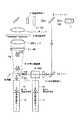
図1は、本発明の第1の実施形態に係わるパターン欠陥検査装置を説明するためのもので、特に光学システムを示す構成図の一例を示している。光学システム以外の構成は、前記図7と同様に構成すればよい。但し、透過光及び反射光の2つの光を検出するため、比較回路68等を2系統設ける必要がある。
【0045】
適当な短波長レーザ光源1から出た光は、まず適当な光源面を得るために、ビームエキスパンダ(図示せず)を経てハエの目レンズ状の多光源発生装置(図示せず)に導かれる。その後、多光源を1つに合成する照明光学系(例えばケーラ照明光学系;図示せず)に導かれる。ここで、レーザ1の光束はS偏光で調整されているものとする。その後、ハーフミラー2で光束は透過用光束(S偏光)と反射用光束(S偏光)に適当な割合で分離される。
【0046】
透過用光束(S偏光)は、λ/4板3,透過光視野絞り4,コンデンサレンズ5を通り、被測定試料6を円偏光で照明する。透過光視野絞り4は、透過光の情報を取りたい部分の領域のみを照射するためのものであり、これにより光源の有効活用を図ることができる。被測定試料6を通過した透過光は、対物レンズ7とλ/4板8を通過してP偏光に偏光される。この透過光は、偏光ビームスプリッタ9(PBS,このPBSはP偏光を透過させる)、空間分離機構10を素通りし、第1の検出光学系11(図では破線で示し詳細は省く、主に倍率等を変更するレンズ系が組み込まれている)により、透過光検出センサ(第1の検出センサ)12に集光される。
【0047】
一方、ハーフミラー2で分離された反射用光束(S偏光)は、適当なミラー13と反射用の視野絞り14を介して偏光ビームスプリッタ9へ導かれる。反射用の視野絞り14は、透過用視野絞り4と異なった領域を照射することによってレーザ光量の有効活用が図られている。偏光ビームスプリッタ9で反射光のS偏光は反射し、λ/4板8と対物レンズ7を経て被測定試料6のパターン面に到着し円偏光となる。これにより、透過光と反射光とが別の光路を経由してきたのに拘わらず、円偏光でパターン面を照射することができる。被測定試料6からの反射光は再度対物レンズ7とλ/4板8を通ってP偏光に偏光される。今度はPBS9を通過し空間分離機構10に入る。
【0048】
空間分離機構10の近傍は被測定試料面の第1結像面になっており、その部分での倍率は本設計では約30倍と被測定試料面より大幅に拡大されている。このため、図に示すように空間分離機構10は単なるミラー構造で簡単に観察視野の空間分離が可能となっている。従って、上述したように視野の半分を透過用パターンの検出、他の半分を反射用パターンの検出に空間的に分離するように照射を行えば、観察視野を有効に使用することができる。そして、空間分離機構10での光学像分離用にミラー15を配置することによって、光量の損失無しに画像の空間分離が簡単に達成できる。
【0049】
本光学システムでは、この部分に結像面を配置したことに特徴がある。ミラー15は完全に結像面に配置して良いが、ミラー面が輝度による劣化やゴミ等の影響が懸念される場合は、図に示すように若干デフォーカスする位置に配置すればよい。
【0050】
空間分離機構10のミラー15により反射した被測定試料面からの反射光は第2の検出光学系16(本構造は透過光用の第1の検出光学系11と同様変倍系で構成されている)に入射し、この光学系16により反射光検出センサ17(第2の検出センサ)に集光される。
【0051】
本方式による光量の有効活用を先の(表1)に追加する形で数値を記入した(新方式と記載)ものを、下記の(表2)に示す。(表2)中に新方式と記しているのが本実施形態である。この(表2)から分かるように本実施形態では、少なくとも従来方式に比べ2倍の光量が得られることになる。反射光学系を実現する上で、この差は非常に有効である。
【0052】
【表2】
本実施形態の光学システムでは、図2に示すように対物レンズの観察視野を分離して使用し、且つ照明視野もその大きさに合わせて照射することで、光源パワーの有効活用が図られている。図中20は対物レンズ結像面における視野を示している。第1、第2の検出センサが観察している領域はそれぞれ21,22で示されている。検出センサとしては、電荷蓄積型のTDIセンサを用いるのが照射エネルギーが少ない場合には最適である。
【0054】
このように配置された時、図のx方向が被測定試料を載せたステージが連続に移動する方向となる。ミラー15の端面の加工精度によって分離できる間隔が決まるが、それ以外の制約によって決まるものでは無い。理論上ほぼ接近してセンサ領域を設定できる。透過光と反射光のバランスはハーフミラー2によって決定することができるが、その分配だけでは十分な反射光量を得られない場合もある。この場合、別々のレーザ光源を準備して光量を得るようにすればよいが、装置が複雑になったり高価となる。
【0055】
ところが、電荷蓄積型のTDIセンサは蓄積段を例えば128段,256段と製作することができるし、256段用のセンサも128段で使用することができる。これにより、光量が少ない場合であっても検査は十分に可能となる。また、透過光検査と反射光検査で透過光検出センサのTDIセンサの蓄積段と反射光検出センサの蓄積段を異ならせて(反射光側の蓄積段を多くして)使用することが、同時検査を実行するときには有効である。この切り替え操作を装置の制御回路から行えるようにして光量に合わせて使用できることは、検査装置として非常に都合のいいものであることは容易に理解できる。
【0056】
第1、第2の検出光学系は図3に示すように、その主な構造は変倍系で構成されている。例えば、第1結像レンズ23は顕微鏡システムにおいて一般にチューブレンズと呼ばれる結像レンズである。その像を変倍リレー系25,26,27によって拡大・縮小しセンサ上に再結像する。変倍リレー系25,26,27は、必ずしも図3に示した構成によらなくとも構成可能である。24は第1結像点、28は最終結像レンズである。
【0057】
これらの検出光学系11,16の主な目的は観察画像取得時の画像の倍率を変更して使用する場合に用いられる。透過光・反射光のそれぞれの検出光学系は本実施形態の場合は、同じ構造で製作されている。これは検査感度と関連して使用される。
【0058】
透過・反射光はそれぞれ独立した検出光学系11,16に導入され、各々の検出センサ12,17に入る。独立した理由の1つは、多くの場合、透過光・反射光が分離できる結像面はセンサ上になり、その場所での透過・反射光分離を行うには光学系全体が大きくなる欠点があることによる。更に、本実施形態のように独立して変倍系を設けた場合、透過検査と反射検査とで倍率を変えて検査を実行することができるためである。
【0059】
検出センサ上で得られる光量は倍率の2乗に反比例するため、ちょっとした倍率変更で足りない分の光量を得ることができる。例えば、透過検査では160倍の拡大率で検査を行い、反射検査で130倍の検査で行った場合、1.5倍の光量が反射側で得られることになる。透過検査を160倍で行っている場合は反射検査での130倍の領域は2割程大きく観察されるが、同じ場所を2重で検査することを許容してしまえば特に大きな問題は残らない。反射検査の方が一般に検出感度は高くなる傾向になるため、倍率が下がっても検査全体に与える影響は少ないといえる。これを、電荷蓄積型のTDIセンサの蓄積段の変更と合わせて使うことで、透過光・反射光同時検査が十分可能となる。
【0060】
上述のようにして得られた透過・反射画像を用いて実際に比較検査する手段には、大きく以下の2つの考え方がある。1つは、図4(a)に示すように、透過光検出センサ12、及び反射光検出センサ17からの出力画像を別々に補正回路30,31で補正した後、比較回路29で検査する方法である。もう1つは、図4(b)に示すように、透過光検出センサ12、及び反射光検出センサ17からの出力画像を補正・合成回路32で、それぞれの画像を補正した後、画像を座標が一致するように合成し、得られた画像を使って比較回路29で検査する方法である。
【0061】
このように、センサ後段に補正回路を設けることにより、グローバルゲイン,ダイナミックゲイン,オフセット等を補正することができる。本実施形態ではこれらに加えて、画像の倍率補正と歪み補正、回転補正、位置補正を行える機能を持つ。
【0062】
第1、第2検出光学系の倍率は正確に製作されたとしても、それぞれ完全に一致しているとは限らない。無論、倍率差を持って検査を実行する場合には補正は確実に必要である。また、透過光・反射光は同一視野内で見ているとはいえ、視野内の歪みによって画像は透過観察領域と反射観察領域とで差が発生する。さらに、反射像と透過像を比較する場合、ある時間では別の座標の画像を、それぞれ観察するために同一座標での画像を処理するためには、それぞれの回路に若干の画像メモリを準備しておく必要がある。それぞれに必要な理由は、被検査物の動きが逆転する場合に対応するためである。
【0063】
また、座標軸を合わせるためにセンサの間隔に相当する位置補正量が必要である。蓄えられた画像メモリから、同一位置の画像を抽出するためには必要な情報であり、検査系の倍率変更を行った場合には、位置補正量は変化するため、それらの情報を指定或いは蓄えておくことも必要となる。同様なことは、倍率補正、歪み補正にも言える。このような機能を持つ光学システムが実用的な透過・反射検査を可能とする。
【0064】
この補正を実現するためには、予めパターンの座標位置が分かっている試料を使って透過像と反射像の倍率差や歪量、回転を含んだ位置の差を測定しておき、これを用いて補正する方法がある。またそれとは別に、検査開始前や検査中に実際のパターンを取り込んで逐次補正しながら検査を行う方法もある。微細なパターンでは透過像と反射像の装置起因の差を測定することは難しいが、比較的大きなパターンを抽出して行えばこれらの測定補正は可能である。
【0065】
このように本実施形態によれば、従来の方法に比べて光源に必要となる光量を小さくでき、且つ確実に透過・反射画像を取得できる。多くの場合、十分な光量が得られない状態での透過光・反射光の検査は不可能であった。実際、透過光のみの検査を実行し、更に反射光の検査は十分な時間をかけて別途行うなど極めて時間を要していた。これらの問題を一挙に解決して透過光・反射光による同時検査を効果的に行うことができる。
【0066】
また、本実施形態のような視野分離は透過光・反射光の分離によって大幅な視野の拡大を必要としない。センサの大きさは長方形的な大きさであるため、従来は視野の中央に置かれていたが若干移動させるだけで2個のセンサを設置することができる。これは、空間分離という方法がなせるメリットであり、原理的にセンサを限りなく密着させることができるように考え出された光学システム・センサシステムである。従って、従来の光学系を大幅な設計変更無しに透過・反射の良好な画像を高速で得ることができる。
【0067】
即ち、本実施形態の構成では、透過・反射を同時に行うことができるために装置の稼動率が大幅に向上する。そして、本実施形態の光学系及びセンサ方式をパターンの欠陥を検査する欠陥検査装置に用いた場合、システムを簡素化でき、信頼性が高く、かつ検出感度の高い欠陥検査を高速に行うことが可能となる。
【0068】
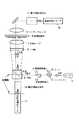
(第2の実施形態)
図5は、本発明の第2の実施形態に係わるパターン欠陥検査装置を説明するためのもので、特に光学システムを示す構成図の一例を示している。なお、図1と同一部分には同一符号を付して、その詳しい説明は省略する。
【0069】
本実施形態においても図1と同様に、レーザ1の光束はS偏光で調整されているものとする。この光束は、ハーフミラー2で透過用光束と反射用光束に適当な割合で分離される。透過用光束は図1と同じ方法で透過光検出センサ(第1の検出センサ)12に集光される。しかし、後述する偏光ビームスプリッタ9は本実施形態では別の位置に設置されている。
【0070】
一方、分離した反射用光束(S偏光)は、適当なミラー13と反射用の視野絞り14を介して偏光ビームスプリッタ9へ導かれるが、その光路は空間分離機構10に向かうようにされている。第1の実施形態と同様に、反射用の視野絞り14は透過用視野絞り4と異なった領域を照射することによって、レーザ光量の有効活用を図るものである。
【0071】
偏光ビームスプリッタ9(ここではS偏光を透過しP偏光を反射するように設置されている)で透過した反射光(S偏光)は空間分離機構10に入る。空間分離機構10の近傍は被測定試料面の第1結像面になっており、その部分での倍率は本設計では約30倍と被測定試料面より大幅に拡大されている。このため、図5に示すように、空間分離機構10は単なるミラー構造で簡単に観察視野の空間分離が可能となっている。
【0072】
ミラー15で反射した反射光束は、λ/4板8、対物レンズ7を経て被測定試料6のパターン面に到着し円偏光となる。これで透過光と反射光とが別の光路を経由してきたのに拘わらず、円偏光でパターン面を照射することができる。被測定試料6の反射光は、再度対物レンズ7とλ/4板8を通ってP偏光に偏光される。そして、空間分離機構10のミラー15に入り、再度反射してPBS9に入射する。光学像分離を図示するようにミラー15を配置する構造とすることによって、光量の損失無しに画像の空間分離が簡単に達成できる。ミラー15は完全に結像面に配置して良いが、ミラー面の輝度による劣化やゴミ等の影響が懸念される場合は、図に示すように若干デフォーカスする位置に配置しても良い。
【0073】
PBS9ではP偏光は反射し、結果的に被測定試料6からの反射光は第2の検出光学系16(本構造は透過光用の第1の検出光学系と同様変倍系で構成されている)に入射し、この光学系16により反射光検出センサ17(第2の検出センサ)に導かれる。
【0074】
本実施形態の場合も、光量損失を纏めた結果は先の(表2)に示した光量となり、従来よりも効果的に反射光を取得することができる。
【0075】
なお、上記第1,第2の実施形態に留まらず、ミラー,ハーフミラー,PBS,空間分離機構等の配置は様々な場合が考えられる。入射光が被測定試料面の一方向から照射された場合でも、同様な空間分離機構を結像面に配置することによって、容易に透過・反射画像を得ることができる。分離は上述したように拡大された結象面で行っているため、ミラー構造空間分離方法が採用でき、透過光・反射光の効率的な分離が可能となっている。
【0076】
(第3の実施形態)
図6は、本発明の第3の実施形態に係わるパターン欠陥検査装置を説明するためのもので、特に光学システムを示す構成図の一例を示している。なお、図1と同一部分には同一符号を付して、その詳しい説明は省略する。
【0077】
レーザ等の光源1からの光束(S波)は、ハーフミラー2により一方は反射用、他方は透過用に別けられる。光量の分配は適宜実際の必要光量の応じて設定される。それぞれの光束は視野絞り4,14を通りPBS9に入りλ/4板8によって回転、対物レンズ7を通して被測定試料6を照明する。この場合の照射領域は、前記図2で示したように視野全体或いは2個のセンサが必要とする領域のみでよい。本実施形態の場合、透過光・反射光は別々に照射されている。ここで、PBS9の配置位置は結像面位置である。こうすることによって、照射領域の分離のためにある強度差を持って確実に照射できる。
【0078】
被測定試料6を透過した光はコンデンサレンズ5を通って第1の検出光学系10を経て透過光検出センサ12に入る。この場合、コンデンサレンズ5は上記対物レンズ並みの高精度化を要求されるため、このシステムでは高価になり不利である欠点を持つ。一方、被測定試料面からの反射光は再度対物レンズ7、λ/4板8を通ってP偏光となり、PBS9を通過し、第2の検出光学系16を経て反射光検出センサ17に入る。
【0079】
このような構成であっても、透過光と反射光の両方に基づいた検査が可能である。
【0080】
なお、本発明は上記実施形態そのままに限定されるものではなく、実施段階ではその要旨を逸脱しない範囲で構成要素を変形して具体化できる。また、上記実施形態に開示されている複数の構成要素の適宜な組み合わせにより、種々の発明を形成できる。例えば、実施形態に示される全構成要素から幾つかの構成要素を削除してもよい。さらに、異なる実施形態にわたる構成要素を適宜組み合わせてもよい。
【0081】
【発明の効果】
以上詳述したように本発明によれば、透過光と反射光の両方を利用してパターン欠陥を検査すると共に、試料のパターン面の光学的結像面近傍に設けられた空間的分離機構により、透過光と反射光とを物理的に分離することによって、透過光と反射光の両方を利用して試料上のパターン欠陥を検査することができ、且つ光量損失を伴うことなく短波長光学系の検査視野の空間分離を行うことができ、光量損失を抑制して感度の良い検査を行うことができる。
【図面の簡単な説明】
【図1】第1の実施形態に係わるパターン欠陥検査装置における光学システムの構成を示す図。
【図2】第1の実施形態における光学システムの観察視野分離方法の一例を示す図。
【図3】第1の実施形態における光学システムの変倍系の構成の一例を示す図。
【図4】第1の実施形態における画像の比較方法を説明するための回路構成を示す図。
【図5】第2の実施形態に係わるパターン欠陥検査装置における光学システムの構成を示す図。
【図6】第3の実施形態に係わるパターン欠陥検査装置における光学システムの構成を示す図。
【図7】パターン欠陥検査装置の基本的な構成を示す図。
【図8】フォトマスクの検査ストライプを説明するための模式図。
【図9】従来のパターン欠陥検査装置における光学システム構成の一例を示す図。
【符号の説明】
1…レーザ光源
2…ハーフミラー
3,8…λ/4板
4…透過光視野絞り
5…コンデンサレンズ
6…被測定試料
7…対物レンズ
9…偏光ビームスプリッタ(PBS)
10…空間分離機構
11…第1の検出光学系
12…透過光検出センサ(第1の検出センサ)
13,15…ミラー
14…反射光視野絞り
16…第2の検出光学系
17…反射光検出センサ(第2の検出センサ)
20…対物レンズ視野
21,22…観察領域
23…第1結像レンズ
24…第1結像点
25,26,27…変倍リレー系
28…最終結像レンズ
29…比較回路
30,31…補正回路
32…補正・合成回路[0001]
BACKGROUND OF THE INVENTION
The present invention relates to a pattern defect inspection apparatus for inspecting pattern defects, and in particular, inspects defects included in patterns such as masks, wafers, and liquid crystal substrates used when manufacturing semiconductor elements and liquid crystal displays (LCDs). The present invention relates to a pattern defect inspection apparatus.
[0002]
[Prior art]
In recent years, in pattern defect inspection devices that perform pattern inspection by comparing design data and measurement data of masks used in the manufacture of large-scale LSIs, the detection sensitivity is improved by installing a reflection optical system in addition to a transmission optical system. The thing which aimed at the improvement of this is developed (nonpatent literature 1). In this apparatus, the wavelength used in the transmitted light inspection and the wavelength used in the reflected light inspection are different from each other, so that the wavelength is separated by a filter in the configured optical system, and each light is put into the transmission / reflection detection sensor.
[0003]
However, in order to increase the detection sensitivity, and further to perform inspection in accordance with the wavelength used in lithography, it is necessary to shorten the inspection wavelength. By shortening the inspection wavelength, the optical lens can be designed. In particular, it has become difficult to design a lens with reduced aberrations at two wavelengths. For this reason, in an inspection apparatus that detects a defect size of 100 nm, there has been a problem that it is difficult to adopt an optical system in which the wavelength of transmission / reflection is changed. Therefore, a need has arisen for a method for obtaining transmission and reflection images using a single wavelength.
[0004]
When observing with both transmitted light and reflected light, it has been generally performed to irradiate the same position coaxially and take an observation image (
[0005]
In addition, a laser is often used as the short wavelength light source, and a polarization separation method is used to separate the laser light. However, in the polarization separation, it is difficult to completely separate the transmission and reflection, and some of each other occurs. The polarization efficiency is decreased in the short wavelength polarization beam splitter, so that the light amount is decreased. Polarization separation (polarization beam splitter, etc.) ) Must be inserted into a part of the optical system, such as a λ / 2 or λ / 4 plate, and it is pointed out that there is a considerable loss of light in this part. Yes. Furthermore, since it is necessary to place an objective lens, which is the most important optical component, at a position facing the sample surface to be measured, the configuration of the optical system becomes very complicated and expensive.
[0006]
On the other hand, there has been proposed an optical system inspection method and apparatus for irradiating a beam within the same field of view of an observation system separately from irradiation for transmitted light and irradiation for reflected light without irradiating the same point with a beam (patent) Reference 3). The method of separating the observation system in the field of view as in this method is a method that covers the weak points of
[0007]
However, this method has a large loss in light quantity, such as an incident beam irradiation method, a visual field separation method, and a method of guiding transmitted light / reflected light to a detection sensor. In particular, there is a drawback that light quantity loss has not been studied in the concept of transmitted light / reflected light separation from the reflected light beam introduction section to the detection sensor. Furthermore, an optical system that can independently change the magnification is not introduced in each portion from the reflected light beam introduction portion to the transmitted light / reflected light detection sensor. Even if the detection sensors are laid out in close proximity and detected, it is difficult to actually put the sensors close to each other because of the balance between the optical magnification required for inspection and the physical size of the sensor. In this part, a method of separating a light beam with a beam splitter has also been proposed, but problems remain such as no consideration of light loss as described above.
[0008]
In the future, when the inspection wavelength is as short as 200 nm or less, the deterioration of the light amount is the most important issue. Furthermore, the above-mentioned document does not consider simultaneous inspection of transmitted light and reflected light by examining the difference in the amount of light that can be obtained between transmitted light and reflected light, and many problems remain in actual operation.
[0009]
Hereinafter, the reduction in the amount of light in the optical system that has been studied in the conventional short wavelength optical system including the configuration of Patent Document 3 will be described. FIG. 9 is a diagram illustrating an example of an optical system that can detect transmitted light and reflected light.
[0010]
The light emitted from the
[0011]
On the other hand, the reflected light beam (2) is bent by the
[0012]
Various arrangements of the polarizing
[0013]
Even if various optical elements are examined from Table 1, it is maximum if a light quantity of about 0.5 at most, that is, half of the amount of light is obtained.
[0014]
[Table 1]
[Patent Document 1]
US Pat. No. 5,572,598
[0016]
[Patent Document 2]
US Pat. No. 5,563,702
[0017]
[Patent Document 3]
Special Publication 2002-501194
[0018]
[Non-Patent Document 1]
Photo mask and X-Ray Mask Technology IV, Vol. 3096 (1997), pp404-414, Performance of cell-shift defect inspection technique
[0019]
[Problems to be solved by the invention]
As described above, in the conventional pattern defect inspection apparatus, although there is an idea of using both transmitted light and reflected light, the light source power necessary for the inspection apparatus has not been effectively used and the wavelength has been shortened. In such a situation, there is a problem that the loss of light amount due to space separation in the inspection visual field is large and the sensitivity is lowered.
[0020]
The present invention has been made in consideration of the above-mentioned circumstances. The object of the present invention is to inspect pattern defects on a sample by using both transmitted light and reflected light, and a short wavelength optical. An object of the present invention is to provide a pattern defect inspection apparatus capable of performing a highly sensitive inspection by suppressing a light amount loss due to spatial separation of a system inspection visual field.
[0021]
[Means for Solving the Problems]
(Constitution)
In order to solve the above problems, the present invention adopts the following configuration.
[0022]
That is, the present invention is a pattern defect inspection apparatus for inspecting a pattern defect using a pattern image obtained by irradiating light to a measurement sample on which a pattern is formed, and the pattern formation surface of the sampleWhen Irradiate the opposite surface with first inspection light of a predetermined wavelength.A first detection optical system; a first detection sensor that detects transmitted light from the sample by irradiation of the first inspection light; and a second that is equal in wavelength to the first inspection light on the pattern forming surface of the sample. A second irradiation optical system that irradiates a different area of the same field of view as the first irradiation light, and a second detection sensor that detects reflected light from the sample due to irradiation of the second inspection light; A mirror provided near the optical imaging plane between the pattern forming surface of the sample and each sensor, and reflects one of transmitted light or reflected light from the sample and guides it to a corresponding detection sensor; and A polarizing beam splitter provided between the pattern forming surface of the sample and the mirror, and reflects the second inspection light to the pattern forming surface of the sample and allows the transmitted light and reflected light from the sample to pass therethrough; , It is characterized by comprising.
[0023]
The present invention also relates to a pattern defect inspection apparatus for inspecting a pattern defect using a pattern image obtained by irradiating light on a sample to be measured on which a pattern is formed, the surface being opposite to the pattern formation surface of the sample A first irradiation optical system for irradiating a first inspection light having a predetermined wavelength, a first detection sensor for detecting transmitted light from the sample by irradiation of the first inspection light, and a pattern forming surface of the sample A second irradiation optical system for irradiating a second inspection light having the same wavelength as that of the first inspection light onto a different region of the same field of view as the first irradiation light; and from the sample by irradiation of the second inspection light. A second detection sensor for detecting reflected light of the sample, and an optical imaging plane between the pattern forming surface of the sample and each sensor,A mirror that reflects reflected light and guides it to a second detection sensor; and is provided between the mirror and the second detection sensor, transmits or reflects second inspection light and guides it to the mirror, and the mirror A polarizing beam splitter that reflects or passes reflected light from the sample obtained via the light beam and guides it to a second detection sensor; It is characterized by comprising.
[0025]
Here, preferred embodiments of the present invention include the following.
[0026]
(1) A first detection optical system that guides the transmitted light separated by the space separation mechanism to the first detection sensor, and a second detection optical that guides the reflected light separated by the space separation mechanism to the second detection sensor And further comprising a system.
[0027]
(2) The second irradiation optical system has a polarization beam splitter provided between the pattern forming surface of the sample and the space separation mechanism, and the polarization beam splitter reflects the second inspection light and reflects the second inspection light. In addition to being guided to the pattern formation surface of the sample, the transmitted light and reflected light from the sample are allowed to pass through.
[0028]
(3) The second irradiation optical system has a polarization beam splitter provided between the space separation mechanism and the second detection sensor, and the polarization beam splitter transmits or reflects the second inspection light. And guiding the light to the second detection sensor by reflecting or passing reflected light from the sample obtained via the space separation mechanism.
[0029]
(4) The optical imaging plane with respect to the pattern formation surface of the sample is an enlarged imaging plane of the observation field at least observed on the pattern formation surface, and a mirror is used as a space separation mechanism, and this mirror is used as the optical imaging plane. It was fixed at a position slightly shifted from
[0030]
(5) Equipped with an XY stage that mounts the sample and moves in the plane XY direction perpendicular to the illumination optical axis. The pattern image acquisition is performed by continuously moving one axis of the XY stage, and a charge accumulation type as a detection sensor. In addition to using a TDI (Time Delay Integration) sensor, the charge accumulation type TDI sensor is different in the accumulation stage of the TDI sensor of the transmitted light detection sensor and the accumulation stage of the reflected light detection sensor in the transmitted light inspection and reflected light inspection. (Use more storage stages on the reflected light side)
[0031]
(6) The first detection optical system and the second detection optical system can independently change the magnification of the observation image, and the first illumination optical system and the second illumination can be changed according to each magnification. The illumination field of view of the optical system can be changed.
[0032]
(7) When the transmitted light inspection and the reflected light inspection are performed simultaneously, the magnification of the first detection optical system through which the transmitted light passes is different from the magnification of the second detection optical system through which the reflected light passes. To do.
[0033]
(8) A function capable of recognizing the position of the first image obtained by the first detection sensor and the position of the second image obtained by the second detection sensor, and the first and second images respectively. At least one of the functions includes brightness adjustment, expansion / contraction (magnification) adjustment, distortion adjustment, rotation adjustment, and the ability to specify the number of sensor accumulation stages. If necessary, transmission pattern inspection, reflection pattern inspection, or transmission pattern and reflection pattern It is possible to carry out inspections using singly or simultaneously.
[0034]
(9) The transmission pattern inspection, the reflection pattern inspection, or the inspection using the transmission pattern and the reflection pattern shall be a die-to-die inspection or a die-to-database inspection.
[0035]
(Function)
According to the present invention, in order to separate transmitted light and reflected light in the detection optical system, a spatial separation mechanism including a total reflection mirror or the like is provided instead of a polarizing beam splitter or the like, and the transmitted light and reflected light from the sample are separated. , Separated from the spatially separated field of view within the pattern viewing field. For this reason, it is possible to prevent a light amount loss from occurring in the detection optical system due to separation of transmitted light and reflected light. Therefore, the pattern defect on the sample can be inspected using both transmitted light and reflected light, and even when short wavelength light is used, the loss of light quantity in the detection optical system is suppressed and the sensitivity is high. Inspection can be performed.
[0036]
DETAILED DESCRIPTION OF THE INVENTION
Before describing embodiments of the invention, a basic configuration of a pattern defect inspection apparatus will be described. FIG. 7 is a diagram illustrating a configuration example of a pattern defect inspection apparatus that performs pattern inspection by comparing design data and measurement data of a mask used for manufacturing a large-scale LSI.
[0037]
In this apparatus, the
[0038]
The
[0039]
The pattern formed on the
[0040]
On the other hand, the design data used when forming the pattern of the
[0041]
The
[0042]
The above device collects the transmitted light from the sample and guides it to the detection system to obtain image data. However, there are some defects that are difficult to detect with the transmitted light alone. It is requested to do. Therefore, in the present invention, both a transmissive optical system and a reflective optical system are provided, and defect inspection is performed based on reflected light simultaneously with transmitted light.
[0043]
The details of the present invention will be described below with reference to the illustrated embodiments.
[0044]
(First embodiment)
FIG. 1 is a diagram for explaining a pattern defect inspection apparatus according to the first embodiment of the present invention, and particularly shows an example of a configuration diagram showing an optical system. The configuration other than the optical system may be configured in the same manner as in FIG. However, in order to detect two lights of transmitted light and reflected light, it is necessary to provide two systems of the
[0045]
In order to obtain an appropriate light source surface, light emitted from an appropriate short wavelength
[0046]
The transmitted light beam (S-polarized light) passes through the λ / 4 plate 3, the transmitted
[0047]
On the other hand, the reflection light beam (S-polarized light) separated by the half mirror 2 is guided to the
[0048]
In the vicinity of the
[0049]
The present optical system is characterized in that an imaging plane is arranged in this portion. The
[0050]
The reflected light from the surface of the sample to be measured reflected by the
[0051]
The following (Table 2) shows numerical values entered in the form of adding the effective use of the light quantity by this method to the previous (Table 1) (described as the new method). This embodiment describes the new method in (Table 2). As can be seen from this (Table 2), in this embodiment, at least twice the amount of light can be obtained as compared with the conventional method. This difference is very effective in realizing a reflective optical system.
[0052]
[Table 2]
In the optical system of the present embodiment, as shown in FIG. 2, the observation field of the objective lens is used separately, and the illumination field is also irradiated in accordance with its size, so that the light source power can be effectively used. Yes. In the figure,
[0054]
When arranged in this way, the x direction in the figure is the direction in which the stage on which the sample to be measured is placed moves continuously. The separation interval is determined by the processing accuracy of the end face of the
[0055]
However, the charge storage type TDI sensor can be manufactured with, for example, 128 stages and 256 stages, and a sensor for 256 stages can also be used with 128 stages. Thereby, even if the amount of light is small, the inspection can be sufficiently performed. In addition, it is possible to use the TDI sensor accumulation stage of the transmitted light detection sensor and the accumulation stage of the reflected light detection sensor differently (increase the accumulation stage on the reflected light side) for transmitted light inspection and reflected light inspection. This is useful when performing inspections. It can be easily understood that this switching operation can be performed from the control circuit of the apparatus so that it can be used according to the amount of light, which is very convenient as an inspection apparatus.
[0056]
As shown in FIG. 3, the main structure of the first and second detection optical systems is a variable power system. For example, the first imaging lens 23 is an imaging lens generally called a tube lens in a microscope system. The image is enlarged / reduced by the variable
[0057]
The main purpose of these detection
[0058]
The transmitted / reflected light is introduced into independent detection
[0059]
Since the amount of light obtained on the detection sensor is inversely proportional to the square of the magnification, a small amount of light can be obtained with a slight change in magnification. For example, when a transmission inspection is performed at a magnification of 160 times and a reflection inspection is performed at a magnification of 130 times, a light amount of 1.5 times is obtained on the reflection side. When the transmission inspection is performed at 160 times, the region of 130 times in the reflection inspection is observed to be about 20% larger, but if the same place is allowed to be inspected twice, no particular problem remains. . Since the reflection inspection generally tends to have higher detection sensitivity, it can be said that the influence on the entire inspection is small even if the magnification is reduced. By using this together with the change of the accumulation stage of the charge accumulation type TDI sensor, the transmitted light / reflected light simultaneous inspection can be sufficiently performed.
[0060]
Means for actually performing the comparative inspection using the transmission / reflection images obtained as described above have the following two concepts. One is a method in which output images from the transmitted
[0061]
As described above, by providing a correction circuit in the subsequent stage of the sensor, global gain, dynamic gain, offset, and the like can be corrected. In addition to these, the present embodiment has a function that can perform image magnification correction, distortion correction, rotation correction, and position correction.
[0062]
Even if the magnifications of the first and second detection optical systems are accurately manufactured, they do not always coincide completely. Of course, the correction is definitely necessary when the inspection is performed with a magnification difference. In addition, although transmitted light and reflected light are viewed in the same visual field, a difference occurs in the image between the transmission observation region and the reflection observation region due to distortion in the visual field. Furthermore, when comparing a reflected image and a transmitted image, in order to process an image at the same coordinate in order to observe an image at a different coordinate at a certain time, a little image memory is prepared in each circuit. It is necessary to keep. The reason necessary for each is to cope with the case where the movement of the inspection object is reversed.
[0063]
Further, in order to align the coordinate axes, a position correction amount corresponding to the sensor interval is required. This information is necessary to extract the image at the same position from the stored image memory. When the magnification of the inspection system is changed, the position correction amount changes. Therefore, the information is designated or stored. It is also necessary to keep it. The same applies to magnification correction and distortion correction. An optical system having such a function enables practical transmission / reflection inspection.
[0064]
In order to realize this correction, the magnification difference, distortion amount, and position difference including rotation of the transmitted image and reflected image are measured using a sample whose pattern coordinate position is known in advance, and this is used. There is a way to correct it. In addition, there is a method in which an actual pattern is taken in and inspected while sequentially correcting it before or during the start of the inspection. Although it is difficult to measure the difference between the transmitted image and the reflected image due to the device with a fine pattern, if a relatively large pattern is extracted, these measurement corrections are possible.
[0065]
As described above, according to the present embodiment, the amount of light required for the light source can be reduced as compared with the conventional method, and a transmitted / reflected image can be obtained with certainty. In many cases, it is impossible to inspect transmitted light and reflected light in a state where a sufficient amount of light cannot be obtained. Actually, it took a very long time to execute only the inspection of the transmitted light and to inspect the reflected light separately for a sufficient time. These problems can be solved all at once, and simultaneous inspection using transmitted light and reflected light can be effectively performed.
[0066]
Further, the field separation as in the present embodiment does not require a significant field expansion by separating transmitted light and reflected light. Since the size of the sensor is a rectangular size, it has been conventionally placed at the center of the field of view, but it is possible to install two sensors with a slight movement. This is an advantage that can be achieved by a method called spatial separation, and is an optical system / sensor system that has been conceived so that the sensor can be brought into close contact in principle. Therefore, it is possible to obtain an image with good transmission and reflection at high speed without significant design change from the conventional optical system.
[0067]
That is, in the configuration of the present embodiment, since the transmission and reflection can be performed simultaneously, the operation rate of the apparatus is greatly improved. When the optical system and sensor system of the present embodiment are used in a defect inspection apparatus that inspects a pattern defect, the system can be simplified, and a defect inspection with high reliability and high detection sensitivity can be performed at high speed. It becomes possible.
[0068]
(Second Embodiment)
FIG. 5 is a diagram for explaining a pattern defect inspection apparatus according to the second embodiment of the present invention, and particularly shows an example of a configuration diagram showing an optical system. In addition, the same code | symbol is attached | subjected to FIG. 1 and an identical part, and the detailed description is abbreviate | omitted.
[0069]
Also in this embodiment, it is assumed that the light beam of the
[0070]
On the other hand, the separated reflection light beam (S-polarized light) is guided to the
[0071]
The reflected light (S-polarized light) transmitted by the polarizing beam splitter 9 (installed so as to transmit S-polarized light and reflect P-polarized light) enters the
[0072]
The reflected light beam reflected by the
[0073]
The
[0074]
Also in the case of the present embodiment, the result of summarizing the light amount loss becomes the light amount shown in (Table 2) above, and the reflected light can be acquired more effectively than in the past.
[0075]
Note that the arrangement of the mirror, the half mirror, the PBS, the space separation mechanism and the like is not limited to the first and second embodiments, and various cases can be considered. Even when the incident light is irradiated from one direction of the sample surface to be measured, a transmission / reflection image can be easily obtained by arranging a similar space separation mechanism on the imaging surface. Since the separation is performed on the enlarged joint surface as described above, the mirror structure space separation method can be adopted, and the transmitted light and the reflected light can be separated efficiently.
[0076]
(Third embodiment)
FIG. 6 is a view for explaining a pattern defect inspection apparatus according to the third embodiment of the present invention, and particularly shows an example of a configuration diagram showing an optical system. In addition, the same code | symbol is attached | subjected to FIG. 1 and an identical part, and the detailed description is abbreviate | omitted.
[0077]
The light beam (S wave) from the
[0078]
The light transmitted through the sample 6 to be measured passes through the condenser lens 5 and enters the transmitted
[0079]
Even with such a configuration, inspection based on both transmitted light and reflected light is possible.
[0080]
Note that the present invention is not limited to the above-described embodiment as it is, and can be embodied by modifying the constituent elements without departing from the scope of the invention in the implementation stage. In addition, various inventions can be formed by appropriately combining a plurality of components disclosed in the embodiment. For example, some components may be deleted from all the components shown in the embodiment. Furthermore, constituent elements over different embodiments may be appropriately combined.
[0081]
【The invention's effect】
As described above in detail, according to the present invention, pattern defects are inspected using both transmitted light and reflected light, and a spatial separation mechanism provided near the optical imaging surface of the pattern surface of the sample is used. By physically separating transmitted light and reflected light, it is possible to inspect pattern defects on the sample using both transmitted light and reflected light, and a short wavelength optical system without any light loss In this way, it is possible to perform spatial separation of the inspection field of view, and to perform inspection with good sensitivity while suppressing light loss.
[Brief description of the drawings]
FIG. 1 is a diagram showing a configuration of an optical system in a pattern defect inspection apparatus according to a first embodiment.
FIG. 2 is a diagram illustrating an example of an observation visual field separation method of the optical system according to the first embodiment.
FIG. 3 is a diagram illustrating an example of a configuration of a zooming system of the optical system according to the first embodiment.
FIG. 4 is a diagram illustrating a circuit configuration for explaining an image comparison method according to the first embodiment;
FIG. 5 is a diagram showing a configuration of an optical system in a pattern defect inspection apparatus according to a second embodiment.
FIG. 6 is a diagram showing a configuration of an optical system in a pattern defect inspection apparatus according to a third embodiment.
FIG. 7 is a diagram showing a basic configuration of a pattern defect inspection apparatus.
FIG. 8 is a schematic diagram for explaining an inspection stripe of a photomask.
FIG. 9 is a diagram showing an example of an optical system configuration in a conventional pattern defect inspection apparatus.
[Explanation of symbols]
1 ... Laser light source
2 ... Half mirror
3,8 ... λ / 4 plate
4 ... Transmitted light field stop
5. Condenser lens
6 ... Sample to be measured
7 ... Objective lens
9 ... Polarizing beam splitter (PBS)
10 ... Space separation mechanism
11: First detection optical system
12 ... Transmitted light detection sensor (first detection sensor)
13, 15 ... Mirror
14 ... Reflected light field stop
16 ... Second detection optical system
17: Reflected light detection sensor (second detection sensor)
20 ... Objective lens field of view
21, 22 ... Observation area
23. First imaging lens
24: First imaging point
25, 26, 27 ... variable power relay system
28. Final imaging lens
29. Comparison circuit
30, 31 ... Correction circuit
32 ... Correction / synthesis circuit
Claims (2)
Translated fromJapanese前記試料のパターン形成面と反対側の面に所定波長の第1の検査光を照射する第1の照射光学系と、
第1の検査光の照射による前記試料からの透過光を検出する第1の検出センサと、
前記試料のパターン形成面に第1の検査光と波長が等しい第2の検査光を第1の照射光とは同一視野の異なる領域に照射する第2の照射光学系と、
第2の検査光の照射による前記試料からの反射光を検出する第2の検出センサと、
前記試料のパターン形成面と前記各センサとの間の光学的結像面近傍に設けられ、前記試料からの透過光又は反射光の一方を反射して対応する検出センサに導くミラーと、
前記試料のパターン形成面と前記ミラーとの間に設けられ、第2の検査光を反射して前記試料のパターン形成面に導くと共に、前記試料からの透過光及び反射光を通過させる偏光ビームスプリッタと、
を具備してなることを特徴とするパターン欠陥検査装置。A pattern defect inspection apparatus that inspects a pattern defect using a pattern image obtained by irradiating light to a measurement sample on which a pattern is formed,
A first irradiation optical system for irradiating a first inspection light having a predetermined wavelength on a surface opposite to the pattern formation surface of the sample;
A first detection sensor for detecting transmitted light from the sample by irradiation of the first inspection light;
A second irradiation optical system for irradiating a second inspection light having the same wavelength as that of the first inspection light onto a pattern forming surface of the sample in a different area of the same field of view as the first irradiation light;
A second detection sensor for detecting reflected light from the sample by irradiation of second inspection light;
A mirror provided near the optical imaging plane between the pattern formation surface of the sample and each sensor, and reflects one of the transmitted light or reflected light from the sample and guides it to the corresponding detection sensor;
A polarizing beam splitter provided between the pattern forming surface of the sample and the mirror, reflects the second inspection light and guides it to the pattern forming surface of the sample, and allows the transmitted light and reflected light from the sample to pass therethrough. When,
A pattern defect inspection apparatus comprising:
前記試料のパターン形成面と反対側の面に所定波長の第1の検査光を照射する第1の照射光学系と、
第1の検査光の照射による前記試料からの透過光を検出する第1の検出センサと、
前記試料のパターン形成面に第1の検査光と波長が等しい第2の検査光を第1の照射光とは同一視野の異なる領域に照射する第2の照射光学系と、
第2の検査光の照射による前記試料からの反射光を検出する第2の検出センサと、
前記試料のパターン形成面と前記各センサとの間の光学的結像面近傍に設けられ、前記試料からの反射光を反射して第2の検出センサに導くミラーと、
前記ミラーと第2の検出センサとの間に設けられ、第2の検査光を透過又は反射して前記ミラーに導くと共に、前記ミラーを介して得られる前記試料から反射光を反射又は通過させて第2の検出センサに導く偏光ビームスプリッタと、
を具備してなることを特徴とするパターン欠陥検査装置。A pattern defect inspection apparatus that inspects a pattern defect using a pattern image obtained by irradiating light to a measurement sample on which a pattern is formed,
A first irradiation optical system for irradiating a first inspection light having a predetermined wavelength on a surface opposite to the pattern formation surface of the sample;
A first detection sensor for detecting transmitted light from the sample by irradiation of the first inspection light;
A second irradiation optical system for irradiating a second inspection light having the same wavelength as that of the first inspection light onto a pattern forming surface of the sample in a different area of the same field of view as the first irradiation light;
A second detection sensor for detecting reflected light from the sample by irradiation of second inspection light;
A mirror provided near the optical imaging plane between the pattern formation surface of the sample and each of the sensors, and reflects a reflected light from the sample and guides it to a second detection sensor;
Provided between the mirror and the second detection sensor, transmits or reflects the second inspection light and guides it to the mirror, and reflects or passes reflected light from the sample obtained through the mirror. A polarizing beam splitter leading to a second detection sensor;
A pattern defect inspection apparatus comprising:
Priority Applications (3)
| Application Number | Priority Date | Filing Date | Title |
|---|---|---|---|
| JP2003096692AJP4220287B2 (en) | 2003-03-31 | 2003-03-31 | Pattern defect inspection system |
| US10/809,409US7372560B2 (en) | 2003-03-31 | 2004-03-26 | Pattern inspection apparatus |
| US12/033,599US7522276B2 (en) | 2003-03-31 | 2008-02-19 | Pattern inspection method |
Applications Claiming Priority (1)
| Application Number | Priority Date | Filing Date | Title |
|---|---|---|---|
| JP2003096692AJP4220287B2 (en) | 2003-03-31 | 2003-03-31 | Pattern defect inspection system |
Related Child Applications (1)
| Application Number | Title | Priority Date | Filing Date |
|---|---|---|---|
| JP2008269795ADivisionJP4734394B2 (en) | 2008-10-20 | 2008-10-20 | Pattern defect inspection system |
Publications (2)
| Publication Number | Publication Date |
|---|---|
| JP2004301751A JP2004301751A (en) | 2004-10-28 |
| JP4220287B2true JP4220287B2 (en) | 2009-02-04 |
Family
ID=33408670
Family Applications (1)
| Application Number | Title | Priority Date | Filing Date |
|---|---|---|---|
| JP2003096692AExpired - LifetimeJP4220287B2 (en) | 2003-03-31 | 2003-03-31 | Pattern defect inspection system |
Country Status (2)
| Country | Link |
|---|---|
| US (2) | US7372560B2 (en) |
| JP (1) | JP4220287B2 (en) |
Families Citing this family (19)
| Publication number | Priority date | Publication date | Assignee | Title |
|---|---|---|---|---|
| JP2006112913A (en)* | 2004-10-14 | 2006-04-27 | Toshiba Corp | Defect inspection equipment |
| JP4185037B2 (en)* | 2004-10-14 | 2008-11-19 | 株式会社東芝 | Defect inspection equipment |
| JP4896394B2 (en)* | 2004-11-22 | 2012-03-14 | 株式会社トプコン | Mask inspection device |
| JP4181159B2 (en)* | 2005-09-29 | 2008-11-12 | 株式会社東芝 | Defect inspection equipment |
| US7528943B2 (en)* | 2005-12-27 | 2009-05-05 | Kla-Tencor Technologies Corporation | Method and apparatus for simultaneous high-speed acquisition of multiple images |
| JP2007279021A (en)* | 2006-03-14 | 2007-10-25 | Hitachi High-Technologies Corp | Optical defect inspection system |
| JP4678601B2 (en)* | 2006-08-15 | 2011-04-27 | 横河電機株式会社 | Drug discovery screening device |
| JP5221858B2 (en)* | 2006-08-30 | 2013-06-26 | 株式会社日立ハイテクノロジーズ | Defect inspection apparatus and defect inspection method |
| JP4224863B2 (en) | 2007-02-02 | 2009-02-18 | レーザーテック株式会社 | Inspection apparatus, inspection method, and pattern substrate manufacturing method |
| JP2008249921A (en) | 2007-03-30 | 2008-10-16 | Advanced Mask Inspection Technology Kk | Reticle defect inspection apparatus and reticle defect inspection method |
| JP4444984B2 (en)* | 2007-04-18 | 2010-03-31 | アドバンスド・マスク・インスペクション・テクノロジー株式会社 | Reticle defect inspection apparatus and inspection method using the same |
| WO2009149103A1 (en)* | 2008-06-03 | 2009-12-10 | Jeong Hwan J | Interferometric defect detection and classification |
| US8094926B2 (en)* | 2008-06-06 | 2012-01-10 | Kabushiki Kaisha Toshiba | Ultrafine pattern discrimination using transmitted/reflected workpiece images for use in lithography inspection system |
| WO2010113228A1 (en) | 2009-03-31 | 2010-10-07 | 株式会社 日立ハイテクノロジーズ | Examining apparatus and examining method |
| JP2011002305A (en)* | 2009-06-17 | 2011-01-06 | Topcon Corp | Circuit pattern defect detection apparatus, circuit pattern defect detection method, and program therefor |
| JP5342537B2 (en)* | 2010-11-09 | 2013-11-13 | 株式会社ニューフレアテクノロジー | Mask inspection device |
| JP5997450B2 (en)* | 2012-02-08 | 2016-09-28 | キヤノン株式会社 | Aberration correction method and aberration correction apparatus |
| JP6759053B2 (en)* | 2016-10-26 | 2020-09-23 | 株式会社ニューフレアテクノロジー | Polarized image acquisition device, pattern inspection device, polarized image acquisition method, and pattern inspection method |
| JP6917208B2 (en)* | 2017-06-19 | 2021-08-11 | 株式会社ニューフレアテクノロジー | Polarized image acquisition device, pattern inspection device, polarized image acquisition method, and pattern inspection method |
Family Cites Families (14)
| Publication number | Priority date | Publication date | Assignee | Title |
|---|---|---|---|---|
| JPS56155802A (en) | 1980-05-06 | 1981-12-02 | Fujitsu Ltd | Recognition device |
| US4886975A (en)* | 1986-02-14 | 1989-12-12 | Canon Kabushiki Kaisha | Surface examining apparatus for detecting the presence of foreign particles on two or more surfaces |
| JP2933736B2 (en)* | 1991-02-28 | 1999-08-16 | キヤノン株式会社 | Surface condition inspection device |
| DE69208413T2 (en) | 1991-08-22 | 1996-11-14 | Kla Instr Corp | Device for automatic testing of photomask |
| US5563702A (en) | 1991-08-22 | 1996-10-08 | Kla Instruments Corporation | Automated photomask inspection apparatus and method |
| US6175645B1 (en) | 1998-01-22 | 2001-01-16 | Applied Materials, Inc. | Optical inspection method and apparatus |
| US6266442B1 (en) | 1998-10-23 | 2001-07-24 | Facet Technology Corp. | Method and apparatus for identifying objects depicted in a videostream |
| JP2000223541A (en)* | 1999-01-27 | 2000-08-11 | Hitachi Ltd | Defect inspection apparatus and method |
| JP3858571B2 (en)* | 2000-07-27 | 2006-12-13 | 株式会社日立製作所 | Pattern defect inspection method and apparatus |
| US6919957B2 (en)* | 2000-09-20 | 2005-07-19 | Kla-Tencor Technologies Corp. | Methods and systems for determining a critical dimension, a presence of defects, and a thin film characteristic of a specimen |
| US6633831B2 (en)* | 2000-09-20 | 2003-10-14 | Kla Tencor Technologies | Methods and systems for determining a critical dimension and a thin film characteristic of a specimen |
| US6850321B1 (en)* | 2002-07-09 | 2005-02-01 | Kla-Tencor Technologies Corporation | Dual stage defect region identification and defect detection method and apparatus |
| US6930770B2 (en)* | 2002-08-08 | 2005-08-16 | Applied Materials, Israel, Ltd. | High throughput inspection system and method for generating transmitted and/or reflected images |
| US7046352B1 (en)* | 2002-10-08 | 2006-05-16 | Kla-Tencor Technologies Corporation | Surface inspection system and method using summed light analysis of an inspection surface |
- 2003
- 2003-03-31JPJP2003096692Apatent/JP4220287B2/ennot_activeExpired - Lifetime
- 2004
- 2004-03-26USUS10/809,409patent/US7372560B2/ennot_activeExpired - Lifetime
- 2008
- 2008-02-19USUS12/033,599patent/US7522276B2/ennot_activeExpired - Lifetime
Also Published As
| Publication number | Publication date |
|---|---|
| US20080151230A1 (en) | 2008-06-26 |
| US7522276B2 (en) | 2009-04-21 |
| US7372560B2 (en) | 2008-05-13 |
| US20040252296A1 (en) | 2004-12-16 |
| JP2004301751A (en) | 2004-10-28 |
Similar Documents
| Publication | Publication Date | Title |
|---|---|---|
| JP4220287B2 (en) | Pattern defect inspection system | |
| US7911599B2 (en) | Reticle defect inspection apparatus and reticle defect inspection method | |
| US8885037B2 (en) | Defect inspection method and apparatus therefor | |
| JP5303217B2 (en) | Defect inspection method and defect inspection apparatus | |
| TWI654486B (en) | Polarized image acquisition device, pattern inspection device, polarized image acquisition method, and pattern inspection method | |
| KR102079420B1 (en) | Integrated multi-pass inspection | |
| WO2010044351A1 (en) | Supersensitization of defect inspection method | |
| JP4324622B2 (en) | Reticle defect inspection apparatus and reticle defect inspection method | |
| JP2008116405A (en) | Defect inspection method and apparatus | |
| TW201821789A (en) | Simultaneous multi-directional laser wafer inspection | |
| JP5571969B2 (en) | Defect inspection method and apparatus | |
| KR102105878B1 (en) | Polarized image obtaining apparatus, pattern inspecting apparatus, polarized image obtaining method and pattern inspecting method | |
| JP2012127856A (en) | Pattern test device and pattern test method | |
| CN115668289B (en) | Design and wafer image correlation by combining information from multiple collection channels | |
| JP2008267903A (en) | Reticle defect inspection apparatus and inspection method using the same | |
| JP5593209B2 (en) | Inspection device | |
| JP6633892B2 (en) | Polarized image acquisition device, pattern inspection device, and polarized image acquisition method | |
| JP4734394B2 (en) | Pattern defect inspection system | |
| JP2005308615A (en) | Surface flaw inspection device | |
| JP6877239B2 (en) | Pattern inspection device and pattern inspection method | |
| JP4590521B1 (en) | Inspection apparatus and inspection method | |
| JP5201443B2 (en) | Surface inspection apparatus and surface inspection method | |
| JP2006250839A (en) | Surface inspection device |
Legal Events
| Date | Code | Title | Description |
|---|---|---|---|
| A621 | Written request for application examination | Free format text:JAPANESE INTERMEDIATE CODE: A621 Effective date:20051121 | |
| A977 | Report on retrieval | Free format text:JAPANESE INTERMEDIATE CODE: A971007 Effective date:20080424 | |
| A131 | Notification of reasons for refusal | Free format text:JAPANESE INTERMEDIATE CODE: A131 Effective date:20080507 | |
| A521 | Request for written amendment filed | Free format text:JAPANESE INTERMEDIATE CODE: A523 Effective date:20080704 | |
| A131 | Notification of reasons for refusal | Free format text:JAPANESE INTERMEDIATE CODE: A131 Effective date:20080819 | |
| A521 | Request for written amendment filed | Free format text:JAPANESE INTERMEDIATE CODE: A523 Effective date:20081020 | |
| TRDD | Decision of grant or rejection written | ||
| A01 | Written decision to grant a patent or to grant a registration (utility model) | Free format text:JAPANESE INTERMEDIATE CODE: A01 Effective date:20081111 | |
| A01 | Written decision to grant a patent or to grant a registration (utility model) | Free format text:JAPANESE INTERMEDIATE CODE: A01 | |
| A61 | First payment of annual fees (during grant procedure) | Free format text:JAPANESE INTERMEDIATE CODE: A61 Effective date:20081113 | |
| FPAY | Renewal fee payment (event date is renewal date of database) | Free format text:PAYMENT UNTIL: 20111121 Year of fee payment:3 | |
| R150 | Certificate of patent or registration of utility model | Free format text:JAPANESE INTERMEDIATE CODE: R150 Ref document number:4220287 Country of ref document:JP Free format text:JAPANESE INTERMEDIATE CODE: R150 | |
| FPAY | Renewal fee payment (event date is renewal date of database) | Free format text:PAYMENT UNTIL: 20121121 Year of fee payment:4 | |
| FPAY | Renewal fee payment (event date is renewal date of database) | Free format text:PAYMENT UNTIL: 20121121 Year of fee payment:4 | |
| R154 | Certificate of patent or utility model (reissue) | Free format text:JAPANESE INTERMEDIATE CODE: R154 | |
| S111 | Request for change of ownership or part of ownership | Free format text:JAPANESE INTERMEDIATE CODE: R313117 | |
| FPAY | Renewal fee payment (event date is renewal date of database) | Free format text:PAYMENT UNTIL: 20121121 Year of fee payment:4 | |
| R350 | Written notification of registration of transfer | Free format text:JAPANESE INTERMEDIATE CODE: R350 | |
| FPAY | Renewal fee payment (event date is renewal date of database) | Free format text:PAYMENT UNTIL: 20131121 Year of fee payment:5 | |
| S531 | Written request for registration of change of domicile | Free format text:JAPANESE INTERMEDIATE CODE: R313531 | |
| R350 | Written notification of registration of transfer | Free format text:JAPANESE INTERMEDIATE CODE: R350 | |
| S111 | Request for change of ownership or part of ownership | Free format text:JAPANESE INTERMEDIATE CODE: R313115 | |
| R350 | Written notification of registration of transfer | Free format text:JAPANESE INTERMEDIATE CODE: R350 | |
| S111 | Request for change of ownership or part of ownership | Free format text:JAPANESE INTERMEDIATE CODE: R313115 | |
| R350 | Written notification of registration of transfer | Free format text:JAPANESE INTERMEDIATE CODE: R350 | |
| EXPY | Cancellation because of completion of term |