JP4219344B2 - Method and apparatus for controlling a circuit with a high-pressure detection device - Google Patents
Method and apparatus for controlling a circuit with a high-pressure detection deviceDownload PDFInfo
- Publication number
- JP4219344B2 JP4219344B2JP2005199707AJP2005199707AJP4219344B2JP 4219344 B2JP4219344 B2JP 4219344B2JP 2005199707 AJP2005199707 AJP 2005199707AJP 2005199707 AJP2005199707 AJP 2005199707AJP 4219344 B2JP4219344 B2JP 4219344B2
- Authority
- JP
- Japan
- Prior art keywords
- transistor
- voltage
- terminal
- circuit
- substrate
- Prior art date
- Legal status (The legal status is an assumption and is not a legal conclusion. Google has not performed a legal analysis and makes no representation as to the accuracy of the status listed.)
- Expired - Fee Related
Links
Images


Classifications
- H—ELECTRICITY
- H02—GENERATION; CONVERSION OR DISTRIBUTION OF ELECTRIC POWER
- H02M—APPARATUS FOR CONVERSION BETWEEN AC AND AC, BETWEEN AC AND DC, OR BETWEEN DC AND DC, AND FOR USE WITH MAINS OR SIMILAR POWER SUPPLY SYSTEMS; CONVERSION OF DC OR AC INPUT POWER INTO SURGE OUTPUT POWER; CONTROL OR REGULATION THEREOF
- H02M1/00—Details of apparatus for conversion
- H02M1/36—Means for starting or stopping converters
- H—ELECTRICITY
- H02—GENERATION; CONVERSION OR DISTRIBUTION OF ELECTRIC POWER
- H02M—APPARATUS FOR CONVERSION BETWEEN AC AND AC, BETWEEN AC AND DC, OR BETWEEN DC AND DC, AND FOR USE WITH MAINS OR SIMILAR POWER SUPPLY SYSTEMS; CONVERSION OF DC OR AC INPUT POWER INTO SURGE OUTPUT POWER; CONTROL OR REGULATION THEREOF
- H02M3/00—Conversion of DC power input into DC power output
- H02M3/22—Conversion of DC power input into DC power output with intermediate conversion into AC
- H02M3/24—Conversion of DC power input into DC power output with intermediate conversion into AC by static converters
- H02M3/28—Conversion of DC power input into DC power output with intermediate conversion into AC by static converters using discharge tubes with control electrode or semiconductor devices with control electrode to produce the intermediate AC
- H02M3/325—Conversion of DC power input into DC power output with intermediate conversion into AC by static converters using discharge tubes with control electrode or semiconductor devices with control electrode to produce the intermediate AC using devices of a triode or a transistor type requiring continuous application of a control signal
- H02M3/335—Conversion of DC power input into DC power output with intermediate conversion into AC by static converters using discharge tubes with control electrode or semiconductor devices with control electrode to produce the intermediate AC using devices of a triode or a transistor type requiring continuous application of a control signal using semiconductor devices only
- H02M3/33507—Conversion of DC power input into DC power output with intermediate conversion into AC by static converters using discharge tubes with control electrode or semiconductor devices with control electrode to produce the intermediate AC using devices of a triode or a transistor type requiring continuous application of a control signal using semiconductor devices only with automatic control of the output voltage or current, e.g. flyback converters
- H—ELECTRICITY
- H03—ELECTRONIC CIRCUITRY
- H03K—PULSE TECHNIQUE
- H03K17/00—Electronic switching or gating, i.e. not by contact-making and –breaking
- H03K17/08—Modifications for protecting switching circuit against overcurrent or overvoltage
- H03K17/082—Modifications for protecting switching circuit against overcurrent or overvoltage by feedback from the output to the control circuit
- H03K17/0822—Modifications for protecting switching circuit against overcurrent or overvoltage by feedback from the output to the control circuit in field-effect transistor switches
- H—ELECTRICITY
- H10—SEMICONDUCTOR DEVICES; ELECTRIC SOLID-STATE DEVICES NOT OTHERWISE PROVIDED FOR
- H10D—INORGANIC ELECTRIC SEMICONDUCTOR DEVICES
- H10D30/00—Field-effect transistors [FET]
- H10D30/80—FETs having rectifying junction gate electrodes
- H10D30/83—FETs having PN junction gate electrodes
- H—ELECTRICITY
- H10—SEMICONDUCTOR DEVICES; ELECTRIC SOLID-STATE DEVICES NOT OTHERWISE PROVIDED FOR
- H10D—INORGANIC ELECTRIC SEMICONDUCTOR DEVICES
- H10D62/00—Semiconductor bodies, or regions thereof, of devices having potential barriers
- H10D62/10—Shapes, relative sizes or dispositions of the regions of the semiconductor bodies; Shapes of the semiconductor bodies
- H10D62/17—Semiconductor regions connected to electrodes not carrying current to be rectified, amplified or switched, e.g. channel regions
- H10D62/343—Gate regions of field-effect devices having PN junction gates
- H—ELECTRICITY
- H10—SEMICONDUCTOR DEVICES; ELECTRIC SOLID-STATE DEVICES NOT OTHERWISE PROVIDED FOR
- H10D—INORGANIC ELECTRIC SEMICONDUCTOR DEVICES
- H10D62/00—Semiconductor bodies, or regions thereof, of devices having potential barriers
- H10D62/10—Shapes, relative sizes or dispositions of the regions of the semiconductor bodies; Shapes of the semiconductor bodies
- H10D62/17—Semiconductor regions connected to electrodes not carrying current to be rectified, amplified or switched, e.g. channel regions
- H10D62/351—Substrate regions of field-effect devices
- H10D62/357—Substrate regions of field-effect devices of FETs
- H—ELECTRICITY
- H10—SEMICONDUCTOR DEVICES; ELECTRIC SOLID-STATE DEVICES NOT OTHERWISE PROVIDED FOR
- H10D—INORGANIC ELECTRIC SEMICONDUCTOR DEVICES
- H10D84/00—Integrated devices formed in or on semiconductor substrates that comprise only semiconducting layers, e.g. on Si wafers or on GaAs-on-Si wafers
- H10D84/01—Manufacture or treatment
- H10D84/0123—Integrating together multiple components covered by H10D12/00 or H10D30/00, e.g. integrating multiple IGBTs
- H10D84/0126—Integrating together multiple components covered by H10D12/00 or H10D30/00, e.g. integrating multiple IGBTs the components including insulated gates, e.g. IGFETs
- H10D84/0156—Manufacturing their doped wells
- H—ELECTRICITY
- H10—SEMICONDUCTOR DEVICES; ELECTRIC SOLID-STATE DEVICES NOT OTHERWISE PROVIDED FOR
- H10D—INORGANIC ELECTRIC SEMICONDUCTOR DEVICES
- H10D84/00—Integrated devices formed in or on semiconductor substrates that comprise only semiconducting layers, e.g. on Si wafers or on GaAs-on-Si wafers
- H10D84/01—Manufacture or treatment
- H10D84/02—Manufacture or treatment characterised by using material-based technologies
- H10D84/03—Manufacture or treatment characterised by using material-based technologies using Group IV technology, e.g. silicon technology or silicon-carbide [SiC] technology
- H10D84/038—Manufacture or treatment characterised by using material-based technologies using Group IV technology, e.g. silicon technology or silicon-carbide [SiC] technology using silicon technology, e.g. SiGe
- H—ELECTRICITY
- H10—SEMICONDUCTOR DEVICES; ELECTRIC SOLID-STATE DEVICES NOT OTHERWISE PROVIDED FOR
- H10D—INORGANIC ELECTRIC SEMICONDUCTOR DEVICES
- H10D84/00—Integrated devices formed in or on semiconductor substrates that comprise only semiconducting layers, e.g. on Si wafers or on GaAs-on-Si wafers
- H10D84/80—Integrated devices formed in or on semiconductor substrates that comprise only semiconducting layers, e.g. on Si wafers or on GaAs-on-Si wafers characterised by the integration of at least one component covered by groups H10D12/00 or H10D30/00, e.g. integration of IGFETs
- H10D84/82—Integrated devices formed in or on semiconductor substrates that comprise only semiconducting layers, e.g. on Si wafers or on GaAs-on-Si wafers characterised by the integration of at least one component covered by groups H10D12/00 or H10D30/00, e.g. integration of IGFETs of only field-effect components
- H10D84/83—Integrated devices formed in or on semiconductor substrates that comprise only semiconducting layers, e.g. on Si wafers or on GaAs-on-Si wafers characterised by the integration of at least one component covered by groups H10D12/00 or H10D30/00, e.g. integration of IGFETs of only field-effect components of only insulated-gate FETs [IGFET]
- H—ELECTRICITY
- H10—SEMICONDUCTOR DEVICES; ELECTRIC SOLID-STATE DEVICES NOT OTHERWISE PROVIDED FOR
- H10D—INORGANIC ELECTRIC SEMICONDUCTOR DEVICES
- H10D30/00—Field-effect transistors [FET]
- H10D30/60—Insulated-gate field-effect transistors [IGFET]
- H10D30/601—Insulated-gate field-effect transistors [IGFET] having lightly-doped drain or source extensions, e.g. LDD IGFETs or DDD IGFETs
- H10D30/603—Insulated-gate field-effect transistors [IGFET] having lightly-doped drain or source extensions, e.g. LDD IGFETs or DDD IGFETs having asymmetry in the channel direction, e.g. lateral high-voltage MISFETs having drain offset region or extended drain IGFETs [EDMOS]
- H—ELECTRICITY
- H10—SEMICONDUCTOR DEVICES; ELECTRIC SOLID-STATE DEVICES NOT OTHERWISE PROVIDED FOR
- H10D—INORGANIC ELECTRIC SEMICONDUCTOR DEVICES
- H10D62/00—Semiconductor bodies, or regions thereof, of devices having potential barriers
- H10D62/10—Shapes, relative sizes or dispositions of the regions of the semiconductor bodies; Shapes of the semiconductor bodies
- H10D62/102—Constructional design considerations for preventing surface leakage or controlling electric field concentration
- H10D62/103—Constructional design considerations for preventing surface leakage or controlling electric field concentration for increasing or controlling the breakdown voltage of reverse-biased devices
- H10D62/105—Constructional design considerations for preventing surface leakage or controlling electric field concentration for increasing or controlling the breakdown voltage of reverse-biased devices by having particular doping profiles, shapes or arrangements of PN junctions; by having supplementary regions, e.g. junction termination extension [JTE]
- H10D62/109—Reduced surface field [RESURF] PN junction structures
- H10D62/111—Multiple RESURF structures, e.g. double RESURF or 3D-RESURF structures
- H—ELECTRICITY
- H10—SEMICONDUCTOR DEVICES; ELECTRIC SOLID-STATE DEVICES NOT OTHERWISE PROVIDED FOR
- H10D—INORGANIC ELECTRIC SEMICONDUCTOR DEVICES
- H10D62/00—Semiconductor bodies, or regions thereof, of devices having potential barriers
- H10D62/10—Shapes, relative sizes or dispositions of the regions of the semiconductor bodies; Shapes of the semiconductor bodies
- H10D62/17—Semiconductor regions connected to electrodes not carrying current to be rectified, amplified or switched, e.g. channel regions
- H10D62/351—Substrate regions of field-effect devices
- H10D62/357—Substrate regions of field-effect devices of FETs
- H10D62/364—Substrate regions of field-effect devices of FETs of IGFETs
- H10D62/378—Contact regions to the substrate regions
- H—ELECTRICITY
- H10—SEMICONDUCTOR DEVICES; ELECTRIC SOLID-STATE DEVICES NOT OTHERWISE PROVIDED FOR
- H10D—INORGANIC ELECTRIC SEMICONDUCTOR DEVICES
- H10D64/00—Electrodes of devices having potential barriers
- H10D64/111—Field plates
Landscapes
- Engineering & Computer Science (AREA)
- Power Engineering (AREA)
- Dc-Dc Converters (AREA)
- Semiconductor Integrated Circuits (AREA)
- Metal-Oxide And Bipolar Metal-Oxide Semiconductor Integrated Circuits (AREA)
- Junction Field-Effect Transistors (AREA)
- Dram (AREA)
- Logic Circuits (AREA)
- Control Of Electrical Variables (AREA)
Description
Translated fromJapanese本発明は、一般に、電子回路中に用いられる制御要素に関し、詳細には、本発明は、高圧パワートランジスタを備えた制御要素に関する。 The present invention relates generally to control elements used in electronic circuits, and in particular, the present invention relates to control elements with high voltage power transistors.
集積化パワートランジスタを備えた制御要素の設計における主要目標の2つは、費用と性能である。費用については、一般に、電子回路中で必要とされる外部部品の数を少なくし、また、さらに小形で、さらに効率的なパワートランジスタを使用すれば減らすことができる。性能については、効率を高めるさらに効率の良いパワートランジスタを採用し、また、製造によるむらを少なくして、パワートランジスタで伝えられるピーク電流などの重要なパラメータをより適切に制御できるようにすることで高めることができる。 Two of the major goals in the design of control elements with integrated power transistors are cost and performance. Costs can generally be reduced by reducing the number of external components required in the electronic circuit and using smaller, more efficient power transistors. In terms of performance, more efficient power transistors are used to increase efficiency, and manufacturing irregularities are reduced so that important parameters such as peak current delivered by power transistors can be controlled more appropriately. Can be increased.
電源は、パワートランジスタを備えた制御要素を利用する電子回路の一例である。或る公知の電源の始動機能は、高圧DCを、ブリッジ整流器から制御回路に供給する抵抗器により果たされる。あいにく、始動機能用抵抗器は、高価であって、かつ電源内に広い領域を必要とし、また、始動機能を完了した後でも、絶えず電力を消費するので、給電の効率を低下させる。公知電源の電流制限機能は、パワートランジスタの電源に直列に入れてある検出抵抗器により実現される。この公知手法の欠点は、パワートランジスタの電源に直列に入れてある検出抵抗器の費用、サイズ、電力消費である。 A power supply is an example of an electronic circuit that utilizes a control element with a power transistor. One known power source start function is performed by a resistor that provides high voltage DC to a control circuit from a bridge rectifier. Unfortunately, the starting function resistor is expensive and requires a large area in the power supply, and even after completing the starting function, it constantly consumes power, thus reducing the efficiency of power supply. The current limiting function of the known power supply is realized by a detection resistor placed in series with the power supply of the power transistor. Disadvantages of this known approach are the cost, size and power consumption of the sense resistor in series with the power transistor power supply.
他の公知電源では、電源チップ内の電圧調整器を使用して、上述の始動機能の抵抗器を取り替える。この電源チップ中の電圧調整器は、始動機能を完了した後ではオフにされ、したがって、上述の電源に固有の余分の電力消費が排除される。しかしながら、電源チップ中の電圧調整器は、電源チップ上で、かなり大きい領域を使用し、さらに、静電放電(ESD)や、安全動作領域(SOA)での損傷も起こしやすい。 In other known power sources, a voltage regulator in the power chip is used to replace the starting function resistor described above. The voltage regulator in this power chip is turned off after completing the starting function, thus eliminating the extra power consumption inherent in the power supply described above. However, the voltage regulator in the power supply chip uses a considerably large area on the power supply chip, and also easily causes damage in electrostatic discharge (ESD) and safe operation area (SOA).
本発明は、限定的ではなく、例示として添付図面に詳細に図示されている。 The present invention is illustrated in detail in the accompanying drawings by way of illustration and not limitation.
高圧検出素子を備えた制御回路を利用する新規な回路が開示されている。以下の説明では、本発明を充分理解するために、特定の細部が多数、記述されている。しかしながら、特定の細部を使用して、本発明を実施する必要はないことが、通常の当業者には明らかになろう。他の場合には、本発明を不明瞭にするのを避けるために、周知の材料または方法については、詳しく説明していない。 A novel circuit is disclosed that utilizes a control circuit with a high voltage sensing element. In the following description, numerous specific details are set forth in order to provide a thorough understanding of the present invention. However, it will be apparent to one of ordinary skill in the art that the specific details need not be used to practice the invention. In other instances, well known materials or methods have not been described in detail in order to avoid obscuring the present invention.
以下の説明は、電源の例を用いて、本発明の恩恵を例示している。これらの手法は、電源への使用に限定されず、例えば、100ボルト以上の高圧印加に用いられる制御要素を採用したどんな電子回路にも適用できることは当業者には明らかになろう。 The following description illustrates the benefits of the present invention with the example of a power supply. It will be apparent to those skilled in the art that these approaches are not limited to use in power supplies, but can be applied to any electronic circuit that employs a control element used to apply high voltages, for example, 100 volts or higher.
一般に、本発明の実施形態による電源は、制御回路とともに、基板中に組み込まれた高圧検出素子を含む。一実施形態では、この高圧検出素子はタップ要素付きのオフライン・トランジスタでよい。本発明の実施形態により、タップ要素付きのオフライン・トランジスタでもたらされる利点は、このようなタップ要素に利用される領域が、パワートランジスタ上よりも、制御回路上の方が安価であることである。他の利点は、パワートランジスタが簡略化されることである。さらに他の利点は、一緒に実装される2つ以上のチップを含むハイブリッド(混成)用途と、単一のトランジスタ・パッケージを含むディスクリート(個別)用途に、同一のパワートランジスタ設計を使用できることである。 In general, a power supply according to an embodiment of the present invention includes a high voltage sensing element incorporated in a substrate along with a control circuit. In one embodiment, the high voltage sensing element may be an off-line transistor with a tap element. An advantage provided by an off-line transistor with a tap element, according to embodiments of the present invention, is that the area utilized for such a tap element is less expensive on the control circuit than on the power transistor. . Another advantage is that the power transistor is simplified. Yet another advantage is that the same power transistor design can be used for hybrid applications involving two or more chips mounted together and for discrete applications involving a single transistor package. .
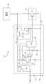
例えば、図1は、外部電圧VEXTERNALに接続されている電源制御要素115と、パワートランジスタ121を示すブロック図である。描かれた実施形態に示されるように、電源制御要素115は、制御回路129と高圧検出素子123が組み込まれている半導体基板117を含む。この図示された実施形態では、パワートランジスタ121は、外部電圧VEXTERNALに接続されており、パワートランジスタ121は、制御回路129に応答して制御される。高圧検出素子123は、外部電圧VEXTERNALを検出するように結合され、制御回路129は、一実施形態において、高圧検出素子123により検出された電圧に応答するように結合されている。For example, FIG. 1 is a block diagram showing a
図2は、本発明の一実施形態により、電源制御要素115の一実施形態を含む電源101の一実施形態の回路図を示している。図示されるように、電源101は、交流(AC)電圧VACを受け取って、整流するように結合された整流器103を含む。コンデンサ105は、整流器103の整流された出力をフィリタリングするために、整流器103の出力部間に結合されている。一実施形態では、電力伝達要素107は、電力整流器103とコンデンサ105による整流電圧を、一次巻線109で受け取るように結合されている。一実施形態では、電力伝達要素107は出力巻線111とバイアス巻線113も含む。電源制御要素115に応答して、電力が、一次巻線109から、出力巻線111とバイアス巻線113に、電力伝達要素107を横切って伝達される。FIG. 2 shows a circuit diagram of an embodiment of the
作動時に、半導体基板117上の制御回路129は、駆動信号を生成して、パワートランジスタ121のスイッチングを制御して、一次巻線109から、出力巻線111とバイアス巻線113への電力伝達を制御する。一実施形態では、制御回路129は、本発明の教示により、電力伝達要素107を通しての電力の伝達を調整するために、パルス幅変調(PWM)回路、サイクル・スキッピング回路(cycle skipping circuitry)、または、パワートランジスタ121のスイッチングを制御するのに適した他の回路を含む。一実施形態では、電源101の出力からのフィードバック情報は、VBIASで提供され、制御回路129により受け取られる。他の実施形態では、本発明の教示により、他の公知手法を用いて、フィードバック情報を基板117の回路に提供してもよいことは理解できるであろう。In operation, the
図2に示される実施形態では、電源制御要素115は、別の第2の基板119上に設けられたパワートランジスタ121とともにパッケージされた第1の基板117上に設けられた回路を含むハイブリッド・パッケージとして示されていることに留意する。他の実施形態では、例えば、第2の基板119上のパワートランジスタ121は、本発明の教示により、第1の基板117とは別にパッケージされる。 In the embodiment shown in FIG. 2, the power
一実施形態では、第1の基板117は、高圧検出デバイスを含む。この高圧検出デバイスは、一実施形態において、パワートランジスタ121に接続されている電圧と同じ外部高圧を受け取るために、一次巻線109に結合された第1の端子を含むトランジスタ123である。図2の実施形態に示されるように、トランジスタ123は、駆動回路150に結合された第2の端子を含む。駆動回路150は、制御回路129から信号151を受け取るように結合されている。一実施形態では、駆動回路150は、信号151に応答してトランジスタ123の動作を制御する。この描かれた実施形態に示されるように、駆動回路150は、さらに接地152にも結合されている。この開示の目的では、接地は、このシステムの他のあらゆる電圧または電位を定めるか、あるいは測定するときの基準電圧または基準電位であると解される。トランジスタ123の第3の端子は、基板117中に設けられた他の回路に電圧を供給する。他の実施形態では、駆動回路150は、基板117中には含まれず、それゆえ、トランジスタ123の第2の端子は、その実施形態では、接地152に直結されている。一実施形態では、トランジスタ123は、ドレイン端子が一次巻線109に結合され、ゲート端子が接地152に接続され、さらに、ソース端子が、基板117中に設けられた他の回路に電圧を供給するタップ端子として役立つ接合形電界効果トランジスタ(JFET)である。一実施形態では、トランジスタ123のJFETは、高圧金属酸化膜半導体電界効果トランジスタ(MOSFET)に組み込まれる。 In one embodiment, the
説明されるように、一実施形態においてトランジスタ123の第3の端子すなわちタップ端子に供給される電圧は、トランジスタ123の第1の端子と第2の端子との間の電圧がトランジスタ123のピンチオフ電圧よりも低いときに、トランジスタ123の第1の端子と第2の端子との間の電圧にほぼ比例する。一実施形態では、トランジスタ123の第3の端子に供給される電圧は、トランジスタ123の第1の端子と第2の端子との間の電圧がトランジスタ123のピンチオフ電圧よりも高いときに、ほぼ一定であって、かつ、トランジスタ123の第1の端子と第2の端子との間の電圧よりも低い。 As described, in one embodiment, the voltage supplied to the third terminal or tap terminal of the
図2に示されるように、基板117上の回路の一実施形態は、トランジスタ125と、トランジスタ123の第3の端子から電圧を受け取るように結合された抵抗器127とを含む。一実施形態では、トランジスタ125を通して得られた電流は、制御回路129により受け取られるように結合され、動作の間、制御回路129に電力を供給し、かつ/または、始動時にコンデンサ131を充電する。例えば、一実施形態では、トランジスタ125をオン状態にすると、トランジスタ123の第1の端子から、トランジスタ123の第3の端子に電流を流して、制御回路129用の始動機能を与えることができる。同様に、制御回路129の動作用の電流を供給するように電流を流し、別の電源が必要とされないように、また、バイアス巻線113が排除されるようにしている。一実施形態では、始動後に、一実施形態におけるコンデンサ131は、動作の間、電力を制御回路129にも供給できる。 As shown in FIG. 2, one embodiment of the circuit on the
一実施形態では、基板117上の回路は、一端が、トランジスタ123の第3の端子から電圧を受け取るように結合された抵抗器135も含む。抵抗器135の他端は、トランジスタ133に結合されている。トランジスタ133は、接地152に接続された抵抗器137に結合されている。比較器139が一方の入力部と他方の入力部を備えている。一方の入力部は、図示されるように、トランジスタ133と抵抗器137との間のノード(接合点)に結合され、また、他方の入力部は、実施形態に示されるように、基準電圧VREFを受け取るように結合されている。一実施形態では、比較器139の出力部は、制御回路129に結合されている。作動時に、トランジスタ133、比較器139、抵抗器135、抵抗器137は、電流制限機能を与えられる。この電流制限機能は、制御回路129で利用されて、パワートランジスタ121を流れる電流を制限し、かつ制御する。In one embodiment, the circuitry on
図2に示される実施形態では、パワートランジスタ121は、説明のために、Nチャネル金属酸化膜半導体電界効果トランジスタ(MOSFET)として図示されていることに留意する。他の実施形態では、例えば、バイポーラ接合形トランジスタ(BJT)、絶縁ゲート形電界効果トランジスタ(IGFET)、サイリスタ素子などの他のタイプの適切なパワートランジスタを利用することができる。 Note that in the embodiment shown in FIG. 2,
基板119上のパワートランジスタ121がオン状態にあるときには、パワートランジスタ121のドレイン上の電圧は、パワートランジスタ121のオン抵抗により、パワートランジスタ121を流れる電流に関係づけられる。トランジスタ123の第3の端子の電圧は、パワートランジスタ121のドレイン上の電圧に比例し、したがって、パワートランジスタ121を流れる電流に比例する。本発明の教示により、トランジスタ123の第3の端子で電圧を検出して、その電圧と、基準レベルVREFを比較することで、電流制限機能が実現される。When the
一実施形態では、基板117上の回路は、トランジスタ123の第3の端子からの電圧と接地152との間に接続されている、分圧器網を形成する抵抗器141と抵抗器143も含む。一実施形態では、抵抗器141と抵抗器143との間のノード(接合点)は、制御回路129に結合されていて、ライン検出機能を提供する。ライン検出機能は、制御回路129で利用されて、一次巻線109のライン電圧を検出する。 In one embodiment, the circuit on
図3は、本発明の教示により、電源制御要素115の他の実施形態の回路図である。図示の実施形態に示されるように、図3に示される回路は、図2に示される回路と類似点を持っている。図3の実施形態に示されるように、トランジスタ123は、JFET245とMOSFET247を含むオフライン・トランジスタである。トランジスタ123の第1の端子は、半導体基板117上で、他の制御回路とともに組み立てられている。半導体基板117は、パワートランジスタ121が組み立てられる半導体基板119とは別の半導体基板である。トランジスタ123は、パワートランジスタ121のドレインと同一の、電力伝達要素107からの外部ノードに結合されている。上で図2に示され、かつ説明されるように、トランジスタ123は、始動、電流制限、ライン検出を含む(ただし、それらには限定されない)いくつかの機能に用いられる。 FIG. 3 is a circuit diagram of another embodiment of a
一実施形態では、MOSFET247は、ゲート、ソース、ボディを、図示されるように互いに結び付けて、つねにオフ状態のままであるように結合されている。それゆえ、MOSFET247のソースは、フローティングではなく、代りに、本発明の教示により、接地152に結び付けられている。ゲート、ソース、ボディが互いに結び付けられた状態では、トランジスタ123の第1の端子は、MOSFET247のドレイン端子であり、トランジスタ123の第2の端子は、MOSFET247のソース端子であり、さらに、トランジスタ123の第3の端子は、JFET245をMOSFET247のドレインに接続することで形成されたタップ端子となっている。 In one embodiment,
上で説明されたように、一実施形態では、オフライン・トランジスタ123の第3の端子すなわちタップ要素の電圧は、或るピンチオフ電圧まで、トランジスタ123の第1の端子の電圧に比例する。トランジスタ123の第1の端子の電圧が、そのピンチオフ電圧を超えると、タップ要素の電圧は、トランジスタ123の第1の端子に現れる可能性のある最大電圧よりもかなり低いと言える電圧で、比較的一定のままである。したがって、トランジスタ123のタップ要素は、トランジスタ123の第1の端子に現れる高圧から、基板117上の他の回路を保護する。 As described above, in one embodiment, the voltage at the third terminal or tap element of
例示される一実施形態では、トランジスタ123のピンチオフ電圧は、例えばブレークダウン電圧が100ボルトよりも低いトランジスタなどの中圧(MV)トランジスタを使用して、トランジスタ123のタップ端子要素を基板117上の他の回路素子に結合できるくらい充分低い電圧である。例えば、この例示される実施形態では、トランジスタ125とトランジスタ133は、高圧トランジスタである必要はない。トランジスタ125とトランジスタ133は、ブレークダウン電圧が例えば10ボルト〜100ボルト程度のMVトランジスタであろうが、一方、トランジスタ123の第1の端子に現れる電圧は、事実上、それよりも高い場合がある。もちろん、ここで与えられる電圧範囲は、説明のためのものであって、本発明の教示により、他の電圧範囲を持つMVトランジスタが利用できるものと理解される。 In one illustrated embodiment, the pinch-off voltage of
一実施形態では、トランジスタ123は、そのブレークダウン電圧がパワートランジスタ121のものよりも高く、この回路中に発生するどんなアバランシェ状態も、パワートランジスタ121で処理されるようにしている。さらに、トランジスタ123は、本来、通常のオフライン・トランジスタよりも堅牢である。なぜなら、トランジスタ123は、普通ならMOSFETのソース/ボディ接合点に結合されている寄生NPNトランジスタを持っていないJFET245を含むからである。さらに、トランジスタ123のゲート、ソース、ボディが互いに結合され、かつ接地152に結び付けられている状態では、トランジスタ123は、つねにオフ状態にあって、トランジスタ123が、トランジスタの堅牢性を劣化させかねないスイッチング過渡動作を絶対に受けないようにしている。 In one embodiment,
図4は、本発明の教示により、高圧電圧検出デバイスの一実施形態の断面側面図を示す図である。特に、図4は、本発明の教示により、高圧JFET323の断面を示している。第1の端子349と第3の端子351は、それぞれ第1の端子ドープ領域350と第3の端子ドープ領域352を介して、P形基板355中のNウェル領域353に接続されている。一実施形態では、第2の端子359とP形基板355は、接地に接続されている。図4の実施形態は、酸化膜層361と酸化膜層363との間で、第1の端子349とNウェル領域353との間の領域の近くにフィールド・プレート365を含むことも示している。一実施形態では、1つまたは複数のP型領域357は、Nウェル領域353内に埋め込まれている。この実施形態に示されたように、いくつかのP形領域357が、第1の端子ドープ領域350と第3の端子ドープ領域352との間のNウェル領域353を横切っている。一実施形態では、P形領域357はP形基板355に電気的に結合されている。他の実施形態では、Nウェル領域353中に、P形領域357がただ1つしかないことがある。P形領域357は、Nウェル領域353中に、または、Nウェル領域353の表面近くに埋め込まれる。さらに他の実施形態では、P形領域357はまったくないことがある。 FIG. 4 is a cross-sectional side view of one embodiment of a high voltage detection device in accordance with the teachings of the present invention. In particular, FIG. 4 shows a cross section of a
一実施形態では、第1の端子349と、第2の端子359またはP形基板355(および、P形領域357)との間の電圧が低いときには、電流は、第1の端子349から、Nウェル領域353を通って、第3の端子351に流れる。第3の端子351の電圧は、第1の端子349の電圧から、Nウェル領域353を流れる電流で発生する電圧降下を引いた値に等しい。第1の端子349の電圧が高くなると、Nウェル領域353中の自由電荷キャリヤ濃度は、P形基板355とP形領域357への逆バイアスによりなくなる。第1の端末349とP形基板355との間の電圧が、或る電圧(すなわち、ピンチオフ電圧)に達すると、その逆バイアスにより、Nウェル領域353の少なくとも一部から、自由電荷キャリアが完全になくなる。このピンチオフ電圧を超えると、第1の端子349と第3の端子351との間のNウェル領域353の抵抗が大幅に大きくなり、本発明の教示により、第3の端子351の電圧が、事実上、ピンチオフ電圧に定着するようにしている。 In one embodiment, when the voltage between the
例えば、図5は、本発明の教示により、パワートランジスタの両端の電圧の関数として、高圧検出デバイスの出力電圧の関係の一実施形態を示す図である。特に、曲線467は、例えばパワートランジスタ121の両端の電圧などのパワートランジスタの両端の電圧が、そのピンチオフ電圧よりも低いときに、例えばトランジスタ123の第3の端子の電圧などの高圧検出素子の出力電圧が、パワートランジスタの両端の電圧にほぼ比例することを示している。しかしながら、パワートランジスタの両端の電圧が、そのピンチオフ電圧よりも高いときには、高圧検出素子の電圧出力は、ほぼ一定である(定着している)か、あるいは、トランジスタの両端の電圧上昇とともに、ほんのわずかに上昇する。この例では、そのピンチオフ電圧は、約50ボルトとして図示されている。もちろん、50ボルトは、説明のためにのみ与えられたものであり、本発明の教示により、ピンチオフ電圧は、他の実施形態において異なる値を取る場合があると理解される。 For example, FIG. 5 is a diagram illustrating one embodiment of the relationship of the output voltage of the high voltage sensing device as a function of the voltage across the power transistor in accordance with the teachings of the present invention. In particular, the
上述の詳細な説明では、本発明は、その特定の模範的な実施形態に関して述べられてきた。しかしながら、本発明のさらに広範な精神および範囲から逸脱しなければ、様々な改造および変更を、それらの実施形態に施せることは明白であろう。よって、本明細書および図面は、限定的なものではなくて、例示するものと見なされるべきである。 In the foregoing detailed description, the invention has been described with reference to specific exemplary embodiments thereof. It will be apparent, however, that various modifications and changes may be made to the embodiments without departing from the broader spirit and scope of the invention. Accordingly, the specification and drawings are to be regarded as illustrative rather than restrictive.
115…電源制御回路、121…パワートランジスタ、123…高電圧検出要素、129…制御回路DESCRIPTION OF
Claims (15)
Translated fromJapanese前記第1のトランジスタの前記第3の端子に結合されている、前記第1の基板中に設けられた制御回路と、
第1の端子が前記外部電圧に接続されている、第2の基板中に設けられた第2のトランジスタと、
を備える回路であって、
前記第1のトランジスタの前記第1の端子と前記第2の端子との間の電圧が、前記第1のトランジスタのピンチオフ電圧よりも低いときには、前記第1のトランジスタの前記第3の端子に供給される電圧が、前記第1のトランジスタの前記第1の端子と前記第2の端子との間の電圧に比例し、また、前記第1のトランジスタの前記第1の端子と前記第2の端子との間の電圧が、前記第1のトランジスタの前記ピンチオフ電圧よりも高いときには、前記第1のトランジスタの前記第3の端子に供給される電圧が一定で、前記第1のトランジスタの前記第1の端子と前記第2の端子との間の電圧よりも低い回路。A first transistor provided in a first substrate having a first terminal, a second terminal, a third terminal, and wherein the first terminal is connected to an external voltage;
A control circuit provided in the first substrate, coupled to the third terminal of the first transistor;
A second transistor provided in a second substrate, wherein a first terminal is connected to the external voltage;
A circuit comprising:
When the voltage between the first terminal and the second terminal of the first transistor is lower than the pinch-off voltage of the first transistor, the voltage is supplied to the third terminal of the first transistor. The voltage to be applied is proportional to the voltage between the first terminal and the second terminal of the first transistor, and the first terminal and the second terminal of the first transistor Is higher than the pinch-off voltage of the first transistor, the voltage supplied to the third terminal of the first transistor is constant, and the first transistor of the first transistor A circuit having a voltage lower than the voltage between the terminal and the second terminal.
前記外部電圧が前記第1のトランジスタのピンチオフ電圧よりも低いときには、前記外部電圧にほぼ比例した出力電圧を前記第1のトランジスタから供給し、また、前記外部電圧が、前記第1のトランジスタの前記ピンチオフ電圧よりも高いときには、一定で、前記外部電圧よりも低い出力電圧を前記第1のトランジスタから供給するステップと、
第2の基板上に設けられた第2のトランジスタを、前記第1の基板上に設けられた制御回路でスイッチングするステップと、
を含む方法。Detecting an external voltage connected to a first transistor provided on a first substrate;
When the external voltage is lower than the pinch-off voltage of the first transistor, an output voltage substantially proportional to the external voltage is supplied from the first transistor, and the external voltage is Supplying an output voltage from the first transistor that is constant and lower than the external voltage when higher than the pinch-off voltage;
Switching a second transistor provided on a second substrate with a control circuit provided on the first substrate;
Including methods.
The method of claim 11, further comprising detecting a line voltage state of a power supply from an output voltage of the first transistor.
Applications Claiming Priority (1)
| Application Number | Priority Date | Filing Date | Title |
|---|---|---|---|
| US10/888,813US7002398B2 (en) | 2004-07-08 | 2004-07-08 | Method and apparatus for controlling a circuit with a high voltage sense device |
Publications (2)
| Publication Number | Publication Date |
|---|---|
| JP2006024945A JP2006024945A (en) | 2006-01-26 |
| JP4219344B2true JP4219344B2 (en) | 2009-02-04 |
Family
ID=34980229
Family Applications (1)
| Application Number | Title | Priority Date | Filing Date |
|---|---|---|---|
| JP2005199707AExpired - Fee RelatedJP4219344B2 (en) | 2004-07-08 | 2005-07-08 | Method and apparatus for controlling a circuit with a high-pressure detection device |
Country Status (3)
| Country | Link |
|---|---|
| US (7) | US7002398B2 (en) |
| EP (2) | EP2557673A2 (en) |
| JP (1) | JP4219344B2 (en) |
Families Citing this family (33)
| Publication number | Priority date | Publication date | Assignee | Title |
|---|---|---|---|---|
| US6865093B2 (en)* | 2003-05-27 | 2005-03-08 | Power Integrations, Inc. | Electronic circuit control element with tap element |
| US7002398B2 (en) | 2004-07-08 | 2006-02-21 | Power Integrations, Inc. | Method and apparatus for controlling a circuit with a high voltage sense device |
| US7425834B2 (en)* | 2005-08-26 | 2008-09-16 | Power Integrations, Inc. | Method and apparatus to select a parameter/mode based on a time measurement |
| EP1885050B1 (en)* | 2006-08-01 | 2010-02-17 | Siemens Aktiengesellschaft | System for determination of the gate voltage of a power fet, and method |
| US8368144B2 (en)* | 2006-12-18 | 2013-02-05 | Infineon Technologies Ag | Isolated multigate FET circuit blocks with different ground potentials |
| US8129815B2 (en) | 2009-08-20 | 2012-03-06 | Power Integrations, Inc | High-voltage transistor device with integrated resistor |
| US8116106B2 (en)* | 2008-09-19 | 2012-02-14 | Power Integrations, Inc. | Method and apparatus to select a parameter/mode based on a measurement during an initialization period |
| US8169801B2 (en)* | 2009-05-28 | 2012-05-01 | Monolithic Power Systems, Inc. | Voltage converters with integrated low power leaker device and associated methods |
| US8154078B2 (en)* | 2010-02-17 | 2012-04-10 | Vanguard International Semiconductor Corporation | Semiconductor structure and fabrication method thereof |
| US8305826B2 (en) | 2010-05-07 | 2012-11-06 | Power Integrations, Inc. | Method and apparatus for programming an anti-fuse element in a high-voltage integrated circuit |
| US8164125B2 (en) | 2010-05-07 | 2012-04-24 | Power Integrations, Inc. | Integrated transistor and anti-fuse as programming element for a high-voltage integrated circuit |
| US7932738B1 (en) | 2010-05-07 | 2011-04-26 | Power Integrations, Inc. | Method and apparatus for reading a programmable anti-fuse element in a high-voltage integrated circuit |
| TWI411205B (en)* | 2010-12-10 | 2013-10-01 | Richtek Technology Corp | Current sense circuit for a switch mode power supply |
| US9048747B2 (en) | 2011-11-23 | 2015-06-02 | Zahid Ansari | Switched-mode power supply startup circuit, method, and system incorporating same |
| US9087713B2 (en) | 2012-10-12 | 2015-07-21 | Power Integrations, Inc. | Semiconductor device with shared region |
| TWI489744B (en)* | 2013-06-03 | 2015-06-21 | Richtek Technology Corp | AC to DC power converter control circuit |
| CN104241278B (en)* | 2013-06-06 | 2016-12-28 | 立锜科技股份有限公司 | AC to DC power converter control circuit |
| US9401612B2 (en) | 2014-09-16 | 2016-07-26 | Navitas Semiconductor Inc. | Pulsed level shift and inverter circuits for GaN devices |
| US9219420B1 (en)* | 2014-11-07 | 2015-12-22 | Power Integrations, Inc. | Overvoltage protection using a tapFET |
| US10784372B2 (en) | 2015-04-03 | 2020-09-22 | Magnachip Semiconductor, Ltd. | Semiconductor device with high voltage field effect transistor and junction field effect transistor |
| KR101975630B1 (en) | 2015-04-03 | 2019-08-29 | 매그나칩 반도체 유한회사 | Semiconductor Structure having a Junction Field Effect Transistor and a High Voltage Transistor and Method for Manufacturing the same |
| KR102313728B1 (en) | 2018-04-09 | 2021-10-15 | 주식회사 키 파운드리 | Semiconductor device with high voltage field effect transistor and junction field effect transistor |
| US9590507B1 (en) | 2015-12-18 | 2017-03-07 | Infineon Technologies Austria Ag | Auxiliary supply for a switched-mode power supply controller using bang-bang regulation |
| CN109155282B (en) | 2016-04-08 | 2023-04-25 | 电力集成公司 | Integrated Resistors for Semiconductor Devices |
| US11430882B2 (en) | 2016-06-24 | 2022-08-30 | Wolfspeed, Inc. | Gallium nitride high-electron mobility transistors with p-type layers and process for making the same |
| US10892356B2 (en) | 2016-06-24 | 2021-01-12 | Cree, Inc. | Group III-nitride high-electron mobility transistors with buried p-type layers and process for making the same |
| US10153702B2 (en) | 2017-02-07 | 2018-12-11 | Infineon Technologies Austria Ag | Switched-mode power supply controller using a single pin for both input voltage sensing and control of power supply charging |
| US10135357B1 (en) | 2017-09-07 | 2018-11-20 | Power Integrations, Inc. | Threshold detection with tap |
| CN110417258A (en)* | 2019-07-05 | 2019-11-05 | 珠海格力电器股份有限公司 | Controllable switching power supply of current limit |
| US11506687B2 (en)* | 2020-07-01 | 2022-11-22 | Semiconductor Components Industries, Llc | Method of forming a semiconductor device |
| US11929428B2 (en) | 2021-05-17 | 2024-03-12 | Wolfspeed, Inc. | Circuits and group III-nitride high-electron mobility transistors with buried p-type layers improving overload recovery and process for implementing the same |
| US12402346B2 (en)* | 2021-05-17 | 2025-08-26 | Wolfspeed, Inc. | Circuits and group III-nitride transistors with buried p-layers and controlled gate voltages and methods thereof |
| US11979090B2 (en) | 2021-08-12 | 2024-05-07 | Power Integrations, Inc. | Power converter controller with branch switch |
Family Cites Families (40)
| Publication number | Priority date | Publication date | Assignee | Title |
|---|---|---|---|---|
| US4263463A (en) | 1973-04-20 | 1981-04-21 | Sumitomo Chemical Company, Limited | Acetylenic secondary alcohols |
| JPS5534885A (en)* | 1978-09-04 | 1980-03-11 | Toko Inc | Switching regulator |
| GB2089119A (en) | 1980-12-10 | 1982-06-16 | Philips Electronic Associated | High voltage semiconductor devices |
| JPH0691444B2 (en)* | 1987-02-25 | 1994-11-14 | 三菱電機株式会社 | Complementary insulated gate inverter |
| US4811075A (en) | 1987-04-24 | 1989-03-07 | Power Integrations, Inc. | High voltage MOS transistors |
| US5014178A (en) | 1990-05-14 | 1991-05-07 | Power Integrations, Inc. | Self powering technique for integrated switched mode power supply |
| GB9025517D0 (en)* | 1990-11-23 | 1991-01-09 | Zed Instr Ltd | Laser engraving apparatus |
| CN1019720B (en) | 1991-03-19 | 1992-12-30 | 电子科技大学 | Power semiconductor device |
| US5386136A (en)* | 1991-05-06 | 1995-01-31 | Siliconix Incorporated | Lightly-doped drain MOSFET with improved breakdown characteristics |
| US5146298A (en) | 1991-08-16 | 1992-09-08 | Eklund Klas H | Device which functions as a lateral double-diffused insulated gate field effect transistor or as a bipolar transistor |
| JP2824706B2 (en)* | 1991-09-27 | 1998-11-18 | 三菱電機株式会社 | Current source circuit and operation method thereof |
| US5285369A (en) | 1992-09-01 | 1994-02-08 | Power Integrations, Inc. | Switched mode power supply integrated circuit with start-up self-biasing |
| US5313381A (en) | 1992-09-01 | 1994-05-17 | Power Integrations, Inc. | Three-terminal switched mode power supply integrated circuit |
| US5282107A (en) | 1992-09-01 | 1994-01-25 | Power Integrations, Inc. | Power MOSFET safe operating area current limiting device |
| US5313082A (en) | 1993-02-16 | 1994-05-17 | Power Integrations, Inc. | High voltage MOS transistor with a low on-resistance |
| DE4309764C2 (en) | 1993-03-25 | 1997-01-30 | Siemens Ag | Power MOSFET |
| JPH0787733A (en) | 1993-09-17 | 1995-03-31 | Fuji Electric Co Ltd | Start-up circuit for stabilized power supply |
| US5521105A (en)* | 1994-08-12 | 1996-05-28 | United Microelectronics Corporation | Method of forming counter-doped island in power MOSFET |
| US5637898A (en) | 1995-12-22 | 1997-06-10 | North Carolina State University | Vertical field effect transistors having improved breakdown voltage capability and low on-state resistance |
| DE59711481D1 (en) | 1996-02-05 | 2004-05-06 | Infineon Technologies Ag | Semiconductor component controllable by field effect |
| DE19611045C1 (en) | 1996-03-20 | 1997-05-22 | Siemens Ag | Field effect transistor e.g. vertical MOS type |
| US5734564A (en) | 1996-07-26 | 1998-03-31 | Lucent Technologies Inc. | High-efficiency switching power converter |
| US6207994B1 (en) | 1996-11-05 | 2001-03-27 | Power Integrations, Inc. | High-voltage transistor with multi-layer conduction region |
| DE19823768A1 (en) | 1998-05-28 | 1999-12-02 | Bosch Gmbh Robert | Smart power component |
| US5998833A (en) | 1998-10-26 | 1999-12-07 | North Carolina State University | Power semiconductor devices having improved high frequency switching and breakdown characteristics |
| DE19918028A1 (en) | 1999-04-21 | 2000-11-02 | Siemens Ag | Semiconductor device |
| US6462971B1 (en) | 1999-09-24 | 2002-10-08 | Power Integrations, Inc. | Method and apparatus providing a multi-function terminal for a power supply controller |
| DE10001394A1 (en) | 2000-01-14 | 2001-07-26 | Infineon Technologies Ag | Circuit arrangement for applying a supply voltage to a load |
| US6259618B1 (en) | 2000-05-03 | 2001-07-10 | Analog And Power Electronics Corp. | Power chip set for a switching mode power supply having a device for providing a drive signal to a control unit upon startup |
| US6781194B2 (en) | 2001-04-11 | 2004-08-24 | Silicon Semiconductor Corporation | Vertical power devices having retrograded-doped transition regions and insulated trench-based electrodes therein |
| AU2002230482A1 (en) | 2000-11-16 | 2002-05-27 | Silicon Wireless Corporation | Discrete and packaged power devices for radio frequency (rf) applications and methods of forming same |
| JP2002157027A (en) | 2000-11-20 | 2002-05-31 | Mitsubishi Electric Corp | Power conversion device and semiconductor device |
| DE10108131A1 (en) | 2001-02-21 | 2002-09-05 | Infineon Technologies Ag | Semiconductor circuit for power supply grid has a control circuit with a load which is switchable over time |
| US6504733B1 (en) | 2001-02-27 | 2003-01-07 | Thomson Licensing S.A. | Switch mode power supply |
| US6635544B2 (en) | 2001-09-07 | 2003-10-21 | Power Intergrations, Inc. | Method of fabricating a high-voltage transistor with a multi-layered extended drain structure |
| US6627958B2 (en) | 2001-12-10 | 2003-09-30 | Koninklijke Philips Electronics N.V. | Lateral high voltage semiconductor device having a sense terminal and method for sensing a drain voltage of the same |
| US7179396B2 (en)* | 2003-03-25 | 2007-02-20 | Molecular Imprints, Inc. | Positive tone bi-layer imprint lithography method |
| US7323417B2 (en)* | 2004-09-21 | 2008-01-29 | Molecular Imprints, Inc. | Method of forming a recessed structure employing a reverse tone process |
| US6865093B2 (en) | 2003-05-27 | 2005-03-08 | Power Integrations, Inc. | Electronic circuit control element with tap element |
| US7002398B2 (en)* | 2004-07-08 | 2006-02-21 | Power Integrations, Inc. | Method and apparatus for controlling a circuit with a high voltage sense device |
- 2004
- 2004-07-08USUS10/888,813patent/US7002398B2/ennot_activeExpired - Lifetime
- 2005
- 2005-07-06EPEP12190349Apatent/EP2557673A2/ennot_activeWithdrawn
- 2005-07-06EPEP05254248Apatent/EP1615324A3/ennot_activeWithdrawn
- 2005-07-08JPJP2005199707Apatent/JP4219344B2/ennot_activeExpired - Fee Related
- 2005-12-23USUS11/318,218patent/US7205824B2/ennot_activeExpired - Fee Related
- 2007
- 2007-03-09USUS11/716,057patent/US7491611B2/ennot_activeExpired - Fee Related
- 2009
- 2009-01-07USUS12/350,147patent/US7696566B2/ennot_activeExpired - Fee Related
- 2010
- 2010-01-15USUS12/688,778patent/US7872304B2/ennot_activeExpired - Lifetime
- 2010-12-21USUS12/975,224patent/US8120097B2/ennot_activeExpired - Fee Related
- 2012
- 2012-02-02USUS13/365,081patent/US8236656B2/ennot_activeExpired - Fee Related
Also Published As
| Publication number | Publication date |
|---|---|
| US20090121779A1 (en) | 2009-05-14 |
| US8236656B2 (en) | 2012-08-07 |
| US7002398B2 (en) | 2006-02-21 |
| US20120139012A1 (en) | 2012-06-07 |
| US7696566B2 (en) | 2010-04-13 |
| EP2557673A2 (en) | 2013-02-13 |
| US20100117718A1 (en) | 2010-05-13 |
| JP2006024945A (en) | 2006-01-26 |
| US20070155062A1 (en) | 2007-07-05 |
| US7205824B2 (en) | 2007-04-17 |
| EP1615324A2 (en) | 2006-01-11 |
| US7491611B2 (en) | 2009-02-17 |
| US8120097B2 (en) | 2012-02-21 |
| US20110089482A1 (en) | 2011-04-21 |
| US20060006916A1 (en) | 2006-01-12 |
| EP1615324A3 (en) | 2010-04-07 |
| US7872304B2 (en) | 2011-01-18 |
| US20060097770A1 (en) | 2006-05-11 |
Similar Documents
| Publication | Publication Date | Title |
|---|---|---|
| JP4219344B2 (en) | Method and apparatus for controlling a circuit with a high-pressure detection device | |
| US7333351B2 (en) | Electronic circuit control element with tap element | |
| JP4031539B2 (en) | Device including load protection circuit against excessive input voltage and load protection method against excessive input voltage | |
| CN107408892B (en) | Semiconductor device for power control | |
| US6738270B2 (en) | Parallel power source system | |
| EP2066032A2 (en) | Power supply control circuit including overvoltage protection circuit | |
| TWI649953B (en) | Switching power supply control system | |
| JP5338026B2 (en) | Switching power supply control IC and switching power supply device | |
| CN110417287A (en) | Rectifier with clamping circuit | |
| US9077256B2 (en) | Method of forming a low power dissipation regulator and structure therefor | |
| JP2001258148A (en) | Overvoltage protective circuit | |
| HK1097114B (en) | Power control system startup and disable method |
Legal Events
| Date | Code | Title | Description |
|---|---|---|---|
| A977 | Report on retrieval | Free format text:JAPANESE INTERMEDIATE CODE: A971007 Effective date:20071022 | |
| A131 | Notification of reasons for refusal | Free format text:JAPANESE INTERMEDIATE CODE: A131 Effective date:20071030 | |
| A601 | Written request for extension of time | Free format text:JAPANESE INTERMEDIATE CODE: A601 Effective date:20080130 | |
| A602 | Written permission of extension of time | Free format text:JAPANESE INTERMEDIATE CODE: A602 Effective date:20080204 | |
| A601 | Written request for extension of time | Free format text:JAPANESE INTERMEDIATE CODE: A601 Effective date:20080229 | |
| A602 | Written permission of extension of time | Free format text:JAPANESE INTERMEDIATE CODE: A602 Effective date:20080305 | |
| A521 | Request for written amendment filed | Free format text:JAPANESE INTERMEDIATE CODE: A523 Effective date:20080321 | |
| TRDD | Decision of grant or rejection written | ||
| A01 | Written decision to grant a patent or to grant a registration (utility model) | Free format text:JAPANESE INTERMEDIATE CODE: A01 Effective date:20081014 | |
| A01 | Written decision to grant a patent or to grant a registration (utility model) | Free format text:JAPANESE INTERMEDIATE CODE: A01 | |
| A61 | First payment of annual fees (during grant procedure) | Free format text:JAPANESE INTERMEDIATE CODE: A61 Effective date:20081111 | |
| FPAY | Renewal fee payment (event date is renewal date of database) | Free format text:PAYMENT UNTIL: 20111121 Year of fee payment:3 | |
| R150 | Certificate of patent or registration of utility model | Free format text:JAPANESE INTERMEDIATE CODE: R150 | |
| FPAY | Renewal fee payment (event date is renewal date of database) | Free format text:PAYMENT UNTIL: 20111121 Year of fee payment:3 | |
| RD02 | Notification of acceptance of power of attorney | Free format text:JAPANESE INTERMEDIATE CODE: R3D02 | |
| FPAY | Renewal fee payment (event date is renewal date of database) | Free format text:PAYMENT UNTIL: 20111121 Year of fee payment:3 | |
| RD04 | Notification of resignation of power of attorney | Free format text:JAPANESE INTERMEDIATE CODE: R3D04 | |
| FPAY | Renewal fee payment (event date is renewal date of database) | Free format text:PAYMENT UNTIL: 20121121 Year of fee payment:4 | |
| FPAY | Renewal fee payment (event date is renewal date of database) | Free format text:PAYMENT UNTIL: 20131121 Year of fee payment:5 | |
| R250 | Receipt of annual fees | Free format text:JAPANESE INTERMEDIATE CODE: R250 | |
| R250 | Receipt of annual fees | Free format text:JAPANESE INTERMEDIATE CODE: R250 | |
| LAPS | Cancellation because of no payment of annual fees |