JP4214950B2 - Printed circuit board support structure - Google Patents
Printed circuit board support structureDownload PDFInfo
- Publication number
- JP4214950B2 JP4214950B2JP2004142592AJP2004142592AJP4214950B2JP 4214950 B2JP4214950 B2JP 4214950B2JP 2004142592 AJP2004142592 AJP 2004142592AJP 2004142592 AJP2004142592 AJP 2004142592AJP 4214950 B2JP4214950 B2JP 4214950B2
- Authority
- JP
- Japan
- Prior art keywords
- circuit board
- piece
- support
- printed circuit
- tightening
- Prior art date
- Legal status (The legal status is an assumption and is not a legal conclusion. Google has not performed a legal analysis and makes no representation as to the accuracy of the status listed.)
- Expired - Fee Related
Links
- 229910000679solderInorganic materials0.000claimsdescription57
- 239000000758substrateSubstances0.000claimsdescription42
- 238000003780insertionMethods0.000claimsdescription22
- 230000037431insertionEffects0.000claimsdescription22
- 238000004080punchingMethods0.000claimsdescription15
- 239000004020conductorSubstances0.000claimsdescription14
- 230000003014reinforcing effectEffects0.000claimsdescription11
- 239000002184metalSubstances0.000description6
- 238000000034methodMethods0.000description5
- 230000002411adverseEffects0.000description3
- 230000000694effectsEffects0.000description3
- 230000000052comparative effectEffects0.000description2
- WABPQHHGFIMREM-UHFFFAOYSA-Nlead(0)Chemical compound[Pb]WABPQHHGFIMREM-UHFFFAOYSA-N0.000description2
- 238000005452bendingMethods0.000description1
- 238000004519manufacturing processMethods0.000description1
- 238000003825pressingMethods0.000description1
- 230000002787reinforcementEffects0.000description1
- 230000000630rising effectEffects0.000description1
- 238000005476solderingMethods0.000description1
- 230000000087stabilizing effectEffects0.000description1
- 230000003313weakening effectEffects0.000description1
Images


Classifications
- H—ELECTRICITY
- H01—ELECTRIC ELEMENTS
- H01R—ELECTRICALLY-CONDUCTIVE CONNECTIONS; STRUCTURAL ASSOCIATIONS OF A PLURALITY OF MUTUALLY-INSULATED ELECTRICAL CONNECTING ELEMENTS; COUPLING DEVICES; CURRENT COLLECTORS
- H01R4/00—Electrically-conductive connections between two or more conductive members in direct contact, i.e. touching one another; Means for effecting or maintaining such contact; Electrically-conductive connections having two or more spaced connecting locations for conductors and using contact members penetrating insulation
- H01R4/58—Electrically-conductive connections between two or more conductive members in direct contact, i.e. touching one another; Means for effecting or maintaining such contact; Electrically-conductive connections having two or more spaced connecting locations for conductors and using contact members penetrating insulation characterised by the form or material of the contacting members
- H01R4/64—Connections between or with conductive parts having primarily a non-electric function, e.g. frame, casing, rail
- H—ELECTRICITY
- H01—ELECTRIC ELEMENTS
- H01R—ELECTRICALLY-CONDUCTIVE CONNECTIONS; STRUCTURAL ASSOCIATIONS OF A PLURALITY OF MUTUALLY-INSULATED ELECTRICAL CONNECTING ELEMENTS; COUPLING DEVICES; CURRENT COLLECTORS
- H01R12/00—Structural associations of a plurality of mutually-insulated electrical connecting elements, specially adapted for printed circuits, e.g. printed circuit boards [PCB], flat or ribbon cables, or like generally planar structures, e.g. terminal strips, terminal blocks; Coupling devices specially adapted for printed circuits, flat or ribbon cables, or like generally planar structures; Terminals specially adapted for contact with, or insertion into, printed circuits, flat or ribbon cables, or like generally planar structures
- H01R12/70—Coupling devices
- H01R12/71—Coupling devices for rigid printing circuits or like structures
- H01R12/712—Coupling devices for rigid printing circuits or like structures co-operating with the surface of the printed circuit or with a coupling device exclusively provided on the surface of the printed circuit
- H01R12/714—Coupling devices for rigid printing circuits or like structures co-operating with the surface of the printed circuit or with a coupling device exclusively provided on the surface of the printed circuit with contacts abutting directly the printed circuit; Button contacts therefore provided on the printed circuit
- H—ELECTRICITY
- H05—ELECTRIC TECHNIQUES NOT OTHERWISE PROVIDED FOR
- H05K—PRINTED CIRCUITS; CASINGS OR CONSTRUCTIONAL DETAILS OF ELECTRIC APPARATUS; MANUFACTURE OF ASSEMBLAGES OF ELECTRICAL COMPONENTS
- H05K7/00—Constructional details common to different types of electric apparatus
- H05K7/14—Mounting supporting structure in casing or on frame or rack
- H05K7/1417—Mounting supporting structure in casing or on frame or rack having securing means for mounting boards, plates or wiring boards
- H05K7/142—Spacers not being card guides
- H—ELECTRICITY
- H05—ELECTRIC TECHNIQUES NOT OTHERWISE PROVIDED FOR
- H05K—PRINTED CIRCUITS; CASINGS OR CONSTRUCTIONAL DETAILS OF ELECTRIC APPARATUS; MANUFACTURE OF ASSEMBLAGES OF ELECTRICAL COMPONENTS
- H05K9/00—Screening of apparatus or components against electric or magnetic fields
- H05K9/0007—Casings
- H05K9/002—Casings with localised screening
- H05K9/0022—Casings with localised screening of components mounted on printed circuit boards [PCB]
Landscapes
- Engineering & Computer Science (AREA)
- Microelectronics & Electronic Packaging (AREA)
- Mounting Of Printed Circuit Boards And The Like (AREA)
Description
Translated fromJapanese本発明は、プリント基板支持構造、特に、プリント基板の板面に備わっている半田盛りパターンをシャーシなどの導体でなる基板支持体の表面に接触させて電気的に導通させることと併せて、その半田盛りパターンと基板支持体との接触箇所でプリント基板を基板支持体に固定してなるプリント基板支持構造に関する。 The present invention provides a printed circuit board support structure, in particular, a method of bringing a solder pile pattern provided on a board surface of a printed circuit board into contact with the surface of a substrate support made of a conductor such as a chassis and making it electrically conductive. The present invention relates to a printed circuit board support structure in which a printed circuit board is fixed to a circuit board support at a contact portion between a solder pile pattern and the circuit board support.
従来、機器解体時に基板をシャーシから取り外しやすくするための基板固定装置が知られていた(たとえば特許文献1参照)。また、取付基板にプリント板を固定する方式として、ねじの締付け力によって取付基板に取り付けた取付具の基台部と挟持片とでプリント板を挾み付けるものや、取付基板に切起し形成した取付片にプリント板をねじ止めするものなどが知られていた(たとえば特許文献2参照)。 Conventionally, there has been known a board fixing device for facilitating removal of a board from a chassis at the time of device disassembly (see, for example, Patent Document 1). In addition, as a method of fixing the printed board to the mounting board, the printed board is sandwiched between the base part of the fixture and the clamping piece attached to the mounting board by the tightening force of the screw, or formed by raising the mounting board. There are known ones in which a printed board is screwed to the mounting piece (for example, see Patent Document 2).
一方、回路基板のシャーシグランドとの接続構造において、回路基板を固定ねじを用いてシャーシグランドに締付け固定する際に、回路基板に形成した半田を締付け固定箇所でシャーシグランドに圧接させるものが知られていた(たとえば特許文献3参照)。また、シャーシに設けたボスに、取付孔の周囲にアース用の半田を設けたプリント基板をネジ止めするものも知られていた(たとえば特許文献4参照)。 On the other hand, in the connection structure of the circuit board to the chassis ground, when the circuit board is fastened and fixed to the chassis ground by using a fixing screw, the solder formed on the circuit board is brought into pressure contact with the chassis ground at the fastening and fixing point. (For example, refer to Patent Document 3). In addition, there has been known a method in which a printed board having a grounding solder provided around a mounting hole is screwed to a boss provided in a chassis (see, for example, Patent Document 4).
ところで、プリント基板を金属シャーシなどの基板支持体に複数箇所で支持固定し、それらの固定箇所でプリント基板と金属シャーシとを電気的に接続させるというプリント基板支持構造を採用する場合、図6及び図7に示した構造を採用することがあった。同図のプリント基板支持構造では、プリント基板1のコーナ部にはねじ挿通孔12とその周囲の板面に形成された半田盛りパターン2とが備わっているのに対し、金属シャーシ3には基板支持体4が備わっていて、基板支持体4の上に載架したプリント基板1のねじ挿通孔12に挿通させた頭付き締付けねじ5を、基板支持体4に備わっているねじ孔41にねじ込んで締め付けてある。そして、半田盛りパターン2のそれぞれの半田21が押し潰される程度の頭付き締付けねじ5の締付け力を利用して、プリント基板1と基板支持体4との間に隙間Sを確保させたまま、半田盛りパターン2と基板支持体4の表面とを圧接させることによってプリント基板1と基板支持体4とを電気的に導通させている。 By the way, when adopting a printed circuit board support structure in which the printed circuit board is supported and fixed at a plurality of locations on a substrate support such as a metal chassis, and the printed circuit board and the metal chassis are electrically connected at those fixed locations, FIG. The structure shown in FIG. 7 may be adopted. In the printed circuit board support structure shown in the figure, the corner portion of the printed
このプリント基板支持構造によると、プリント基板1を基板支持体4にねじ止めすることとプリント基板1を基板支持体4に電気的に導通させることとが同時に実現されるだけでなく、プリント基板1と基板支持体4との電気的導通信頼性や電気的導通安定性が向上するという利点がある。
しかしながら、図6及び図7を参照して説明したプリント基板支持構造をプリント基板1の複数箇所、たとえば矩形のプリント基板1の4つのコーナ部のそれぞれに対して適用すると、各コーナ部では、頭付き締付けねじ5による締付けトルクのばらつきや半田盛りパターン2の半田21の盛り上がり高さのばらつきなどに起因して、プリント基板1と基板支持体4との間の隙間Sにばらつきが生じることがある。そして、その隙間Sにばらつきが生じると、プリント基板1の4つのコーナ部に対応している基板支持体4の高さが高精度で一致しているとしても、プリント基板1の取付寸法精度が低下し、そのプリント基板1に反りが発生して曲げ応力が残留しやすくなる。 However, if the printed circuit board support structure described with reference to FIGS. 6 and 7 is applied to a plurality of locations of the printed
一方、図8に例示したように、プリント基板1としては、ボールグリッドアレイ(BGA)6を実装したものがある。BGA6は、その下面に配列された端子とソルダーボールとを備えていて、プリント基板に実装するときにはソルダーボールを溶融させることによって上記端子とプリント基板1の導体パターンとを接続するものであるため、BGA6を搭載したプリント基板1がいびつな反り変形を起こしていたりすると、BGAが経時的にプリント基板の板面から浮き上がって上記端子と上記導体パターンとの接続箇所が剥離したり破壊したりするおそれが生じ、そのことが機器の信頼性を大幅に低下させる要因になる。なお、図8は図6で説明した支持構造による取付箇所を示していて、12はねじ挿通孔、2は半田盛りパターンである。On the other hand, as illustrated in FIG. 8, as the printed
この点に関し、上掲の特許文献1や特許文献2は、プリント基板をシャーシなどに固定する構造だけを提供しているに過ぎず、特許文献3や特許文献4は、プリント基板の半田盛り部を図6又は図7で説明したものに準じた構造を採用して基板支持体に電気的に導通させているに過ぎないものであるため、これらの特許文献に記載されている技術をどのように組み合わせたとしても、基板支持体に対するプリント基板の固定箇所でプリント基板と金属シャーシとを電気的に接続させる場合に発生するおそれのあるプリント基板の反りを防ぐことはできない。 In this regard, the above-mentioned
そこで、図6及び図7で説明したプリント基板支持構造において、半田盛りパターン2を省略することにより、プリント基板1の板面のランドを基板支持体4に直接に重ね合わせて上記した隙間Sを生じさせない支持構造を採用することも考えられる。この構造を採用すると、上記隙間Sが存在しなくなるので、プリント基板1の取付寸法精度が向上してプリント基板1に反りが発生しにくくなるという長所がある。しかし、その反面で、プリント基板1と基板支持体4との電気的導通信頼性や電気的導通安定性が低下するという短所が生まれる。この短所を補うために、プリント基板1からリード線などの別部品を介して基板支持体4に対する電気的導通を図るということが行われているけれども、そのようにすると、リード線が余分に必要になって部品点数や作業工数が増大して製造コストが高くなるという欠点や、電気的接続経路が長くなるために接続インピーダンスが高くなって電気的性能が低下するという欠点が生じる。 Therefore, in the printed circuit board support structure described with reference to FIGS. 6 and 7, by omitting the
また、表裏両面に導体パターンを備えたプリント基板の表面の導体パターンを、金属ねじを介してシャーシに電気的に接続することも行われている。しかし、これによっても電気的接続経路が比較的長くなって、特に高周波領域での接続インピーダンスに悪影響を及ぼすおそれがある。 In addition, a conductor pattern on the surface of a printed circuit board provided with a conductor pattern on both the front and back surfaces is electrically connected to the chassis via a metal screw. However, this also makes the electrical connection path relatively long, which may adversely affect the connection impedance particularly in the high frequency region.
そこで、本発明は、リード線などの余分の部品を用いる必要がなく、接続インピーダンスの増大を来さず、高周波領域での接続インピーダンスに悪影響を及ぼすことがないという長所を備えた図6又は図7で説明したような支持構造、すなわち、プリント基板を導体でなる基板支持体に締付け具により締付けて固定し、その締付け箇所でプリント基板の板面に備わっている半田盛りパターンを基板支持体の表面に圧接させるというプリント基板支持構造を採用することを基本として、プリント基板に反りが発生するおそれを無くすることのできるプリント基板支持構造を提供することを目的とする。 Therefore, the present invention does not require the use of extra parts such as lead wires, does not increase the connection impedance, and does not adversely affect the connection impedance in the high frequency region. 7, that is, a printed circuit board is fixed to a substrate support made of a conductor by a fastening tool, and a solder pile pattern provided on the plate surface of the printed circuit board is fixed to the substrate support at the tightening position. An object of the present invention is to provide a printed circuit board support structure that can eliminate the possibility of warping of the printed circuit board based on the use of the printed circuit board support structure that is brought into pressure contact with the surface.
請求項1に係る発明のプリント基板支持構造は、プリント基板を導体でなる基板支持体に締付け具により締付けて固定し、かつ、その締付け具による締付け箇所でプリント基板の板面に備わっている半田盛りパターンが上記基板支持体の表面に接触して上記基板支持体に電気的に導通しているプリント基板支持構造であって、上記締付け具が頭付き締付けねじであり、上記半田盛りパターンが、プリント基板のコーナ部に開設されたねじ挿通孔の周囲に備わり、シャーシでなる上記基板支持体にプリント基板の基準位置を規制する基準支持面を備えた片持ち状の支持片が一体に具備され、その支持片の下側に、その支持片を打ち抜くことによって形成された片持ち状の締付け片が配備されていると共に、上記支持片に補強リブを具備させてその支持片を補強し、かつ、上記締付け片の根元部分に凹入状の欠除部を具備させてその根元部分の有効幅を狭めることによりその締付け片の耐変形強度を上記支持片の耐変形強度よりも弱めてあり、上記半田盛りパターン形成箇所の周囲を上記基準支持面に載架してなる上記プリント基板の上記ねじ挿通孔に挿通された頭付き締付けねじが、上記締付け片に具備されているねじ孔にねじ込まれて締め付けられ、その締付け力により、上記支持片に形成されている締付け片の打抜き跡としての開口を通して配備された上記半田盛りパターンに上記締付け片が変形を伴って圧接している。In the printed circuit board support structure according to the first aspect of the present invention, the printed circuit board is fixed to the substrate support made of a conductor by fastening with a fastening tool, and the solder provided on the plate surface of the printed circuit board at a fastening position by the fastening tool. A printed circuit board support structure in which a raised pattern is in contact with the surface of the substrate support and is electrically connected to the substrate support, wherein the fastener is a headed tightening screw, and the solder pile pattern is A cantilevered support piece provided with a reference support surface for restricting the reference position of the printed circuit board is integrally provided on the board support body made of a chassis, which is provided around a screw insertion hole provided in a corner portion of the printed circuit board. A cantilevered clamping piece formed by punching the supporting piece is provided below the supporting piece, and the supporting piece is provided with a reinforcing rib. Reinforcing the support piece and reducing the effective width of the base part by providing a concave notch in the base part of the clamp piece, thereby reducing the deformation resistance of the clamp piece. A fastening screw with a head that is weaker than the strength and is inserted into the screw insertion hole of the printed board that is mounted on the reference support surface around the solder pile pattern forming portion is provided in the fastening piece. The tightening piece is pressed against the solder pile pattern provided through the opening as a punching trace of the tightening piece formed on the support piece with deformation by the tightening force. is doing.
請求項2に係る発明のプリント基板支持構造は、プリント基板を導体でなる基板支持体に締付け具により締付けて固定し、かつ、その締付け具による締付け箇所でプリント基板の板面に備わっている半田盛りパターンが上記基板支持体の表面に接触して上記基板支持体に電気的に導通しているプリント基板支持構造であって、上記締付け具が頭付き締付けねじであり、上記半田盛りパターンが、プリント基板のコーナ部に開設されたねじ挿通孔の周囲に備わり、シャーシでなる上記基板支持体にプリント基板の基準位置を規制する基準支持面を備えた片持ち状の支持片が一体に具備され、その支持片の下側に、その支持片を打ち抜くことによって形成された片持ち状の締付け片が配備されていると共に、上記支持片に補強リブを具備させてその支持片を補強することにより上記締付け片の耐変形強度を上記支持片の耐変形強度よりも弱めてあり、上記半田盛りパターン形成箇所の周囲を上記基準支持面に載架してなる上記プリント基板の上記ねじ挿通孔に挿通された頭付き締付けねじが、上記締付け片に具備されているねじ孔にねじ込まれて締め付けられ、その締付け力により、上記支持片に形成されている締付け片の打抜き跡としての開口を通して配備された上記半田盛りパターンに上記締付け片が変形を伴って圧接している。According to a second aspect of the present invention, there is provided a printed circuit board support structure in which a printed circuit board is fixed to a substrate substrate made of a conductor by a fastening tool, and solder is provided on a plate surface of the printed circuit board at a fastening position by the fastening tool. A printed circuit board support structure in which a raised pattern is in contact with the surface of the substrate support and is electrically connected to the substrate support, wherein the fastener is a headed tightening screw, and the solder pile pattern is A cantilevered support piece provided with a reference support surface for restricting the reference position of the printed circuit board is integrally provided on the board support body made of a chassis, which is provided around a screw insertion hole provided in a corner portion of the printed circuit board. A cantilevered clamping piece formed by punching the supporting piece is provided below the supporting piece, and the supporting piece is provided with a reinforcing rib. The printed circuit board, in which the deformation strength of the tightening piece is weakened from the deformation strength of the support piece by reinforcing the support piece, and the periphery of the solder pile pattern forming portion is mounted on the reference support surface The head tightening screw inserted into the screw insertion hole is screwed into the screw hole provided in the tightening piece and tightened, and by the tightening force, the punching trace of the tightening piece formed on the support piece is recorded. The fastening pieces are in pressure contact with the solder pile pattern provided through the openings with deformation.
請求項3に係る発明のプリント基板支持構造は、プリント基板を導体でなる基板支持体に締付け具により締付けて固定し、かつ、その締付け具による締付け箇所でプリント基板の板面に備わっている半田盛りパターンが上記基板支持体の表面に接触して上記基板支持体に電気的に導通しているプリント基板支持構造であって、上記締付け具が頭付き締付けねじであり、上記半田盛りパターンが、プリント基板のコーナ部に開設されたねじ挿通孔の周囲に備わり、シャーシでなる上記基板支持体にプリント基板の基準位置を規制する基準支持面を備えた片持ち状の支持片が一体に具備され、その支持片の下側に、その支持片を打ち抜くことによって形成された片持ち状の締付け片が配備されていると共に、上記締付け片の根元部分に凹入状の欠除部を具備させてその根元部分の有効幅を狭めることによりその締付け片の耐変形強度を上記支持片の耐変形強度よりも弱めてあり、上記半田盛りパターン形成箇所の周囲を上記基準支持面に載架してなる上記プリント基板の上記ねじ挿通孔に挿通された頭付き締付けねじが、上記締付け片に具備されているねじ孔にねじ込まれて締め付けられ、その締付け力により、上記支持片に形成されている締付け片の打抜き跡としての開口を通して配備された上記半田盛りパターンに上記締付け片が変形を伴って圧接している。According to a third aspect of the present invention, there is provided a printed circuit board support structure in which a printed circuit board is fixed to a substrate support made of a conductor by a fastening tool, and the solder provided on the plate surface of the printed circuit board at a fastening position by the fastening tool. A printed circuit board support structure in which a raised pattern is in contact with the surface of the substrate support and is electrically connected to the substrate support, wherein the fastener is a headed tightening screw, and the solder pile pattern is A cantilevered support piece provided with a reference support surface for restricting the reference position of the printed circuit board is integrally provided on the board support body made of a chassis, which is provided around a screw insertion hole provided in a corner portion of the printed circuit board. A cantilevered clamping piece formed by punching out the supporting piece is disposed below the supporting piece, and a concave notch is formed at the base of the clamping piece. The deformation resistance strength of the tightening piece is weaker than the deformation resistance strength of the support piece by narrowing the effective width of the root portion by providing a portion, and the periphery of the solder piling pattern forming portion is used as the reference support surface. A headed tightening screw inserted into the screw insertion hole of the printed circuit board mounted is screwed into a screw hole provided in the tightening piece and tightened, and formed on the support piece by the tightening force. The clamping piece is pressed against the solder pile pattern provided through an opening as a punched trace of the clamping piece with deformation.
請求項1、請求項2及び請求項3の発明によると、プリント基板が載架された基準支持面によってプリント基板の取付寸法精度が高精度に保たれる。また、プリント基板の半田盛りパターンには、締付け具によって締め付けられる締付け片の表面が圧接しているので、プリント基板と基板支持体とが締付け片を介して確実に電気的接続されて電気的導通信頼性と電気的導通安定性とが確保される。言い換えると、この構成によると、プリント基板と基板支持体との電気的接続を確実に行わせるための締付け具による締付け力のばらつきの影響や半田盛りパターンの盛り上がり高さのばらつきの影響がプリント基板の取付寸法精度に及ばなくなるので、高い電気的導通信頼性と電気的導通安定性とを確保した上で、取付け後のプリント基板に反りが発生することを確実に防止することが可能になる。According to the first, second, and third aspectsof the present invention, the mounting dimensional accuracy of the printed circuit board is kept high by the reference support surface on which the printed circuit board is mounted. In addition, since the surface of the fastening piece to be clamped by the fastening tool is in pressure contact with the solder pile pattern of the printed board, the printed board and the board support are reliably electrically connected via the fastening piece for electrical conduction. Reliability and electrical conduction stability are ensured. In other words, according to this configuration, the printed circuit board is affected by variations in the tightening force due to the tightening tool and the rise in the height of the solder bump pattern to ensure electrical connection between the printed circuit board and the substrate support. Therefore, it is possible to reliably prevent warping of the printed circuit board after mounting while ensuring high electrical conduction reliability and electrical conduction stability.
本発明では、上記基準支持面を備えた支持片の下側に、その支持片を打ち抜くことによって形成された上記締付け片が配備されていて、支持片に形成されている締付け片の打抜き跡としての開口を通して配備された上記半田盛りパターンに上記締付け片の表面が圧接されている。このため、基板支持体が基準支持面を備えた支持片と締付け片とにより分かれ、プリント基板と基板支持体との電気的接続を確実かつ安定化するための半田盛りパターンが締付け片だけに接触する形態になって、締付け具による締付け力のばらつきの影響や半田盛りパターンの盛り上がり高さのばらつきの影響がプリント基板の取付寸法精度に及ばなくなり、高い電気的導通信頼性と電気的導通安定性とを確保した上で、取付け後のプリント基板に反りが発生することを確実に防止することが可能になる。また、締付け片は、支持片を打抜くことによって形成されているので、余分に部品を追加する必要もない。In the present invention, the fastening piece formed by punching out the support piece is provided on the lower side of the support piece having the reference support surface, and the punching trace of the fastening piece formed in the support piece is provided. The surface of the fastening piece is pressed against the solder pile pattern provided through the opening. For this reason, the substrate support is divided into a support piece with a reference support surface and a fastening piece, and the solder pile pattern for ensuring and stabilizing the electrical connection between the printed circuit board and the board support contacts only the fastening piece. Therefore, the influence of the variation in tightening force due to the fastener and the effect of the variation in the height of the raised solder pattern do not reach the mounting dimension accuracy of the printed circuit board, resulting in high electrical conduction reliability and electrical conduction stability. In addition, it is possible to reliably prevent warping of the printed circuit board after mounting. Further, since the fastening piece is formed by punching the support piece, it is not necessary to add extra parts.
本発明では、上記締付け具が頭付き締付けねじであり、上記半田盛りパターンが、プリント基板の端部に開設されたねじ挿通孔の周囲に備わり、そのねじ挿通孔に挿通された上記頭付き締付けねじを上記締付け片に具備されているねじ孔にねじ込んで締め付けることによりその締付け片を変形させて上記半田盛りパターンに圧接させているという構成を採用している。このため、図6又は図7を参照して説明したプリント基板支持構造における基板支持体4の構造を変更するだけで済む。In the present invention, the tightening tool is a headed tightening screw, and the solder pile pattern is provided around a screw insertion hole provided at an end of the printed circuit board, and the headed tightening inserted through the screw insertion hole. A configuration is adopted in which a screw is screwed into a screw hole provided in the tightening piece and is tightened to deform the tightening piece and press the solder pattern. Therefore, it is only necessary to change the structure of the
本発明では、上記締付け片の耐変形強度を上記支持片の耐変形強度よりも弱めてあるので、締付けねじを締め付ける工程を行うだけで、耐変形強度が支持片のそれよりも弱い締付け片が変形して、支持片の基準支持面に載架されているプリント基板の板面の半田盛りパターンに圧接する。In the present invention,since the deformation resistance strength of the clamping piece is weaker than the deformation resistance strength of the support piece, a clamping piece having a deformation resistance strength weaker than that of the support piece can be obtained simply by performing the process of tighteningthe fastening screw. Deformation is brought into pressure contact with the solder pile pattern on the plate surface of the printed circuit board mounted on the reference support surface of the support piece.
以上説明したように、本発明によれば、プリント基板を導体でなる基板支持体に締付け具により締付けて固定し、その締付け箇所でプリント基板の板面に備わっている半田盛りパターンを基板支持体の表面に圧接させるというプリント基板支持構造を採用しているので、リード線などの余分の部品を用いる必要がなく、接続インピーダンスの増大を来さず、高周波領域での接続インピーダンスに悪影響を及ぼすことがないという長所を備えたプリント基板支持構造を提供することができるだけにとどまらず、取付け後のプリント基板に反りの発生するおそれが無くなって機器の信頼性を容易に向上させることができるという卓越した効果が奏される。また、本発明は、BGAを搭載したプリント基板に適用することによって、プリント基板の反りに起因するプリント基板からのBGAの経時的な剥離や接続箇所の破壊などを生じるおそれがなくなるという効果も奏される。 As described above, according to the present invention, a printed circuit board is fastened and fixed to a board support made of a conductor by a fastening tool, and the solder pile pattern provided on the plate surface of the printed board at the tightened portion is fixed to the board support. Adopts a printed circuit board support structure that presses against the surface of the wire, so there is no need to use extra parts such as lead wires, so that the connection impedance does not increase and the connection impedance in the high-frequency region is adversely affected. It is not only possible to provide a printed circuit board support structure with the advantage that there is no problem, but it is also excellent that the reliability of the equipment can be easily improved without the possibility of warping the printed circuit board after mounting An effect is produced. Further, when the present invention is applied to a printed circuit board on which a BGA is mounted, there is also an effect that there is no possibility that the BGA peels off from the printed circuit board due to warping of the printed circuit board or the connection portion is broken. Is done.
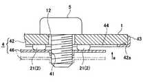
図1は本発明に係るプリント基板支持構造の実施形態を示した概略分解斜視図、図2は基板支持体4の平面図、図3はプリント基板支持構造の概略平面図、図4は図3のIV−IV線に沿う部分の拡大断面図、図5は図4の要部の拡大図である。 1 is a schematic exploded perspective view showing an embodiment of a printed circuit board support structure according to the present invention, FIG. 2 is a plan view of a circuit
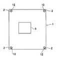
図1のように、プリント基板1のコーナ部にねじ挿通孔12が備わっていると共に、プリント基板1の板面上のねじ挿通孔12の周囲に半田盛りパターン2が形成されている。この半田盛りパターン2は、プリント基板1に形成されているアース接続用導体パターンのランド上に形成されていて、図例では、個々の半田21が放射方向に延びているけれども、半田21の形状は、ねじ挿通孔12を取り囲むリング状であっても、ドット状であっても、その他の形状であってもよい。 As shown in FIG. 1, a
基板支持体4は、図4のように金属シャーシ3に切起し形成されていて、立上り片部31の上端から片持ち状に水平に延び出た矩形の支持片42と、その支持片42を打ち抜くことによって片持ち状に形成されてその支持片42の下側に配備された略矩形の締付け片46とを備えている。支持片42は、その上面が平坦な基準支持面42a(図4又は図5参照)として形成されていて、その基準支持面42aにプリント基板1を載架すると、そのプリント基板1が高精度で位置決めされるようになっていると共に、基準支持面42aに載架されたプリント基板1側の半田盛りパターン2が、支持片42に形成されている締付け片46の打抜き跡としての開口44を通してその下側に突出して締付け片46に上方から対峙するようになっている。また、図例では、締付け片46の耐変形強度が支持片42の耐変形強度よりも弱くなっている。すなわち、支持片42は、その2辺に上向きに曲成された補強リブ43によって耐変形強度が高められているのに対し、締付け片46は、その根元部分の一部に凹入状の欠除部47を具備させることによりその根元部分の有効幅を調節してその耐変形強度を弱めてある。また、締付け片46には、頭付き締付けねじ5をねじ込むためのねじ孔41が備わっている。 As shown in FIG. 4, the
そして、図3又は図4のように、コーナ部を支持片42の基準支持面42aに載架したプリント基板1のねじ挿通孔12に頭付き締付けねじ5を挿通させてその頭付き締付けねじ5を締付け片46のねじ孔41にねじ込んで締め付けてある。また、頭付き締付けねじ5の締付け力によって、図5に矢印aで示したように締付け片46を仮想線の位置から実線の位置まで変形させて半田盛りパターン2に圧接させている。この場合の頭付き締付けねじ5の締付けトルクは、締付け片46が圧接した半田盛りパターン2の半田21が少し押し潰される程度の強さであり、その程度の強さにしておくと、半田盛りパターン2を介してプリント基板1が締付け片46に確実に電気的に接触して良好な電気的導通信頼性と電気的接続安定性とが確保される。 Then, as shown in FIG. 3 or FIG. 4, the headed tightening
この実施形態によると、プリント基板1が載架された支持片42の基準支持面42aによってプリント基板の取付寸法精度が高精度に保たれることに加えて、プリント基板1の半田盛りパターン2には、頭付き締付けねじ5によって締め付けられた締付け片46の表面が圧接してプリント基板1と締付け片46を備える基板支持体4との電気的導通信頼性と電気的導通安定性とが確保される。そのため、プリント基板1の複数箇所、たとえば矩形のプリント基板1の4つのコーナ部を上記構成で基板支持体4によって支持させた場合に、プリント基板1と基板支持体4との電気的接続を確実に行わせるための頭付き締付けねじ5による締付けトルクにばらつきがあっても、また、半田盛りパターン2の盛り上がり高さにばらつきがあっても、それらの影響がプリント基板1の取付寸法精度に及ばない。したがって、高い電気的導通信頼性と電気的導通安定性とを確保した上で、取付け後のプリント基板1に反りの発生するおそれが無くなる。そのため、図8で説明したように、プリント基板1がBGA6を搭載していても、プリント基板1の反りに起因するプリント基板1からのBGA6の経時的な剥離や接続箇所の破壊などを生じるおそれがなくなる。 According to this embodiment, the mounting dimension accuracy of the printed circuit board is maintained at a high accuracy by the
この実施形態では、締付け片46の耐変形強度を支持片42のそれよりも弱めるための手段として、支持片42を補強リブ43により補強してその耐変形強度を高める一方で、締付け片46の根元部分の一部に凹入状の欠除部47を具備させてその耐変形強度を弱めるという手段を採用しているけれども、当該手段はこの実施形態に限定されない。たとえば、支持片42に補強リブ43を設けなくても、支持片42の根元部分の有効幅を締付け片46の根元部分の有効幅よりも広くしておくだけでも、締付け片46の耐変形強度を支持片42のそれよりも弱めることが可能であるし、支持片42に補強リブ43を設けるだけ、あるいは、締付け片46の根元部分の有効幅を狭めるだけでも、締付け片46の耐変形強度を支持片42のそれよりも弱めることが可能である。 In this embodiment, as a means for weakening the deformation resistance of the clamping
1 プリント基板
2 半田盛りパターン
4 基板支持体(シャーシ)
5 頭付き締付けねじ(締付け具)
12 ねじ挿通孔
41 ねじ孔
42 支持片
42a 基準支持面
43 補強リブ
44 開口
46 締付け片
47 欠除部1 Printed
5 Clamping screw with head (clamp)
12
Claims (3)
Translated fromJapanese上記締付け具が頭付き締付けねじであり、上記半田盛りパターンが、プリント基板のコーナ部に開設されたねじ挿通孔の周囲に備わり、シャーシでなる上記基板支持体にプリント基板の基準位置を規制する基準支持面を備えた片持ち状の支持片が一体に具備され、その支持片の下側に、その支持片を打ち抜くことによって形成された片持ち状の締付け片が配備されていると共に、上記支持片に補強リブを具備させてその支持片を補強し、かつ、上記締付け片の根元部分に凹入状の欠除部を具備させてその根元部分の有効幅を狭めることによりその締付け片の耐変形強度を上記支持片の耐変形強度よりも弱めてあり、
上記半田盛りパターン形成箇所の周囲を上記基準支持面に載架してなる上記プリント基板の上記ねじ挿通孔に挿通された頭付き締付けねじが、上記締付け片に具備されているねじ孔にねじ込まれて締め付けられ、その締付け力により、上記支持片に形成されている締付け片の打抜き跡としての開口を通して配備された上記半田盛りパターンに上記締付け片が変形を伴って圧接していることを特徴とするプリント基板支持構造。The printed circuit board is fixed to the board support made of a conductor with a fastening tool, and the solder pile pattern provided on the board surface of the printed circuit board comes into contact with the surface of the board support at the tightening position by the fastening tool. A printed circuit board support structure electrically connected to the substrate support,
The tightening tool is a headed tightening screw, and the solder pile pattern is provided around a screw insertion hole formed in a corner portion of the printed circuit board, and regulates a reference position of the printed circuit board on the substrate support body formed of a chassis. A cantilevered support piece having a reference support surface is integrally provided, and a cantilevered fastening piece formed by punching out the support piece is disposed below the support piece. The supporting piece is provided with reinforcing ribs to reinforce the supporting piece, and the base part of the fastening piece is provided with a recessed notched part to reduce the effective width of the base part, thereby reducing the fastening piece. The deformation resistance is weaker than the deformation resistance of the support piece,
A headed tightening screw inserted through the screw insertion hole of the printed circuit board, which is mounted around the solder support pattern forming portion on the reference support surface, is screwed into a screw hole provided in the tightening piece. The tightening piece is pressed against the solder pile pattern provided through the opening as a punching trace of the tightening piece formed on the support piece with deformation by the tightening force. Printed circuit board support structure.
上記締付け具が頭付き締付けねじであり、上記半田盛りパターンが、プリント基板のコーナ部に開設されたねじ挿通孔の周囲に備わり、シャーシでなる上記基板支持体にプリント基板の基準位置を規制する基準支持面を備えた片持ち状の支持片が一体に具備され、その支持片の下側に、その支持片を打ち抜くことによって形成された片持ち状の締付け片が配備されていると共に、上記支持片に補強リブを具備させてその支持片を補強することにより上記締付け片の耐変形強度を上記支持片の耐変形強度よりも弱めてあり、
上記半田盛りパターン形成箇所の周囲を上記基準支持面に載架してなる上記プリント基板の上記ねじ挿通孔に挿通された頭付き締付けねじが、上記締付け片に具備されているねじ孔にねじ込まれて締め付けられ、その締付け力により、上記支持片に形成されている締付け片の打抜き跡としての開口を通して配備された上記半田盛りパターンに上記締付け片が変形を伴って圧接していることを特徴とするプリント基板支持構造。The printed circuit board is fixed to the board support made of a conductor with a fastening tool, and the solder pile pattern provided on the board surface of the printed circuit board comes into contact with the surface of the board support at the tightening position by the fastening tool. A printed circuit board support structure electrically connected to the substrate support,
The tightening tool is a headed tightening screw, and the solder pile pattern is provided around a screw insertion hole formed in a corner portion of the printed circuit board, and regulates a reference position of the printed circuit board on the substrate support body formed of a chassis. A cantilevered support piece having a reference support surface is integrally provided, and a cantilevered fastening piece formed by punching out the support piece is disposed below the support piece. By providing the support piece with reinforcing ribs and reinforcing the support piece, the deformation resistance of the fastening piece is weaker than the deformation resistance of the support piece,
A headed clamping screw inserted into the screw insertion hole of the printed circuit board, which is mounted around the solder support pattern forming portion on the reference support surface, is screwed into the screw hole provided in the clamping piece. The tightening piece is pressed against the solder pile pattern provided through the opening as a punching trace of the tightening piece formed on the support piece by the tightening force with deformation. Printed circuit board support structure.
上記締付け具が頭付き締付けねじであり、上記半田盛りパターンが、プリント基板のコーナ部に開設されたねじ挿通孔の周囲に備わり、シャーシでなる上記基板支持体にプリント基板の基準位置を規制する基準支持面を備えた片持ち状の支持片が一体に具備され、その支持片の下側に、その支持片を打ち抜くことによって形成された片持ち状の締付け片が配備されていると共に、上記締付け片の根元部分に凹入状の欠除部を具備させてその根元部分の有効幅を狭めることによりその締付け片の耐変形強度を上記支持片の耐変形強度よりも弱めてあり、
上記半田盛りパターン形成箇所の周囲を上記基準支持面に載架してなる上記プリント基板の上記ねじ挿通孔に挿通された頭付き締付けねじが、上記締付け片に具備されているねじ孔にねじ込まれて締め付けられ、その締付け力により、上記支持片に形成されている締付け片の打抜き跡としての開口を通して配備された上記半田盛りパターンに上記締付け片が変形を伴って圧接していることを特徴とするプリント基板支持構造。The printed circuit board is fixed to the board support made of a conductor with a fastening tool, and the solder pile pattern provided on the board surface of the printed circuit board comes into contact with the surface of the board support at the tightening position by the fastening tool. A printed circuit board support structure electrically connected to the substrate support,
The tightening tool is a headed tightening screw, and the solder pile pattern is provided around a screw insertion hole formed in a corner portion of the printed circuit board, and regulates a reference position of the printed circuit board on the substrate support body formed of a chassis. supporting piece of a cantilever having a reference support surface is provided integrally, the under side of the support piece,together with its supporting piececantilevered clamping pieces formed by punching ais deployed, the The deformation strength of the tightening piece is made weaker than the deformation resistance of the support piece by providing a concave notched portion at the root portion of the tightening piece and narrowing the effective width of the root portion,
A headed clamping screw inserted into the screw insertion hole of the printed circuit board, which is mounted around the solder support pattern forming portion on the reference support surface, is screwed into the screw hole provided in the clamping piece. The tightening pieceis pressed against the solder pile pattern provided through the opening as a punching trace of the tightening piece formed on the support pieceby the tightening forcewith deformation. Printed circuit board support structure.
Priority Applications (2)
| Application Number | Priority Date | Filing Date | Title |
|---|---|---|---|
| JP2004142592AJP4214950B2 (en) | 2004-05-12 | 2004-05-12 | Printed circuit board support structure |
| US11/127,783US6994586B2 (en) | 2004-05-12 | 2005-05-12 | Printed circuit board supporting structure |
Applications Claiming Priority (1)
| Application Number | Priority Date | Filing Date | Title |
|---|---|---|---|
| JP2004142592AJP4214950B2 (en) | 2004-05-12 | 2004-05-12 | Printed circuit board support structure |
Publications (2)
| Publication Number | Publication Date |
|---|---|
| JP2005327812A JP2005327812A (en) | 2005-11-24 |
| JP4214950B2true JP4214950B2 (en) | 2009-01-28 |
Family
ID=35375777
Family Applications (1)
| Application Number | Title | Priority Date | Filing Date |
|---|---|---|---|
| JP2004142592AExpired - Fee RelatedJP4214950B2 (en) | 2004-05-12 | 2004-05-12 | Printed circuit board support structure |
Country Status (2)
| Country | Link |
|---|---|
| US (1) | US6994586B2 (en) |
| JP (1) | JP4214950B2 (en) |
Families Citing this family (15)
| Publication number | Priority date | Publication date | Assignee | Title |
|---|---|---|---|---|
| WO2006106827A1 (en)* | 2005-03-31 | 2006-10-12 | Pioneer Corporation | Case body and electric apparatus |
| US20070015121A1 (en)* | 2005-06-02 | 2007-01-18 | University Of Southern California | Interactive Foreign Language Teaching |
| CN100531543C (en)* | 2005-09-09 | 2009-08-19 | 鸿富锦精密工业(深圳)有限公司 | Grounding device for reducing electromagnetic interference |
| JP4241854B2 (en) | 2007-05-22 | 2009-03-18 | 船井電機株式会社 | Board mounting structure |
| CN201130740Y (en)* | 2007-08-17 | 2008-10-08 | 富士康(昆山)电脑接插件有限公司 | Electrical Connector Assembly |
| JP2009212124A (en)* | 2008-02-29 | 2009-09-17 | Toshiba Corp | Printed-circuit board, method of forming frame ground of printed-circuit board, and electronic apparatus |
| TWI395518B (en)* | 2009-09-08 | 2013-05-01 | Compal Electronics Inc | Stack structure of circuit board |
| JP2012152534A (en)* | 2011-01-25 | 2012-08-16 | Kawamura Trading:Kk | Ornament |
| TWI436720B (en)* | 2011-12-26 | 2014-05-01 | Acer Inc | Electronic device and its connecting mechanism |
| JP2014116554A (en)* | 2012-12-12 | 2014-06-26 | Nippon Seiki Co Ltd | Electronic controller |
| JP6732616B2 (en)* | 2016-09-20 | 2020-07-29 | 日立オートモティブシステムズ株式会社 | Electronic control unit |
| CN108173011A (en)* | 2017-11-29 | 2018-06-15 | 华勤通讯技术有限公司 | Metal shell and electronic equipment |
| US10167891B1 (en)* | 2018-03-08 | 2019-01-01 | International Business Machines Corporation | Self-reporting, grounded nut-clip |
| TWI765624B (en)* | 2021-03-26 | 2022-05-21 | 啓碁科技股份有限公司 | Electronic device and fastening structure thereof |
| CN120712900A (en)* | 2023-03-13 | 2025-09-26 | 罗伯特·博世有限公司 | Electronic control device |
Family Cites Families (7)
| Publication number | Priority date | Publication date | Assignee | Title |
|---|---|---|---|---|
| JPH085733B2 (en) | 1987-12-16 | 1996-01-24 | 株式会社竹中工務店 | Inorganic heat insulating material |
| JP2933845B2 (en)* | 1995-02-17 | 1999-08-16 | 三菱電機株式会社 | Printed circuit board mounting device |
| US6560119B1 (en)* | 1998-06-23 | 2003-05-06 | Fujitsu Limited | Fastening parts suitable for recycling |
| JP3042621B1 (en) | 1999-01-27 | 2000-05-15 | セイコーエプソン株式会社 | Connection structure with chassis ground of circuit board |
| US6280202B1 (en)* | 1999-09-01 | 2001-08-28 | Thomas & Betts International, Inc. | Board-to-board alignment and securement device |
| JP2002217502A (en) | 2001-01-12 | 2002-08-02 | Anritsu Corp | Fixing part structure of printed board, and its manufacturing method |
| JP2002299860A (en) | 2001-03-30 | 2002-10-11 | Fujitsu General Ltd | Substrate fixing device |
- 2004
- 2004-05-12JPJP2004142592Apatent/JP4214950B2/ennot_activeExpired - Fee Related
- 2005
- 2005-05-12USUS11/127,783patent/US6994586B2/ennot_activeExpired - Fee Related
Also Published As
| Publication number | Publication date |
|---|---|
| US20050260888A1 (en) | 2005-11-24 |
| US6994586B2 (en) | 2006-02-07 |
| JP2005327812A (en) | 2005-11-24 |
Similar Documents
| Publication | Publication Date | Title |
|---|---|---|
| JP4214950B2 (en) | Printed circuit board support structure | |
| JP4524291B2 (en) | Flat type ground terminal and its surface mounting method | |
| US20060057869A1 (en) | Connector and electronic apparatus having the same | |
| JP5551206B2 (en) | Board device | |
| US6887114B2 (en) | Electrical connector with high performance contacts | |
| WO2014141990A1 (en) | Substrate reinforcing structure | |
| JP3784019B2 (en) | connector | |
| US20090071683A1 (en) | Electronic device mounting structure and method of making the same | |
| JP3505908B2 (en) | Conductive wire connection terminal | |
| JP4487755B2 (en) | Printed circuit board support structure | |
| CN1527657A (en) | Circuit board assembly | |
| JP3635585B2 (en) | Wiring pattern connection method and structure of flexible printed circuit board | |
| KR20100115641A (en) | Fpcb and assembling structure of fpcb | |
| JP2007134407A (en) | Circuit board | |
| JP2006114646A (en) | Circuit board equipment | |
| US6655018B2 (en) | Technique for surface mounting electrical components to a circuit board | |
| JP2006093549A (en) | Electronic apparatus comprising grounding land in printed circuit board | |
| CN101300914A (en) | Connection part structure of circuit board | |
| JP5308687B2 (en) | Mounting structure of surface mount connector to printed circuit board | |
| JP3751944B2 (en) | connector | |
| JP3237648B2 (en) | Short-circuit jig | |
| JP2003257520A (en) | Push-type board connector | |
| JP3001320B2 (en) | Mounting method of surface mount type connector | |
| JP5158568B2 (en) | Conductive structure of metal core substrate | |
| JPH09213387A (en) | Connection terminals for printed wiring boards |
Legal Events
| Date | Code | Title | Description |
|---|---|---|---|
| A621 | Written request for application examination | Free format text:JAPANESE INTERMEDIATE CODE: A621 Effective date:20060201 | |
| A977 | Report on retrieval | Free format text:JAPANESE INTERMEDIATE CODE: A971007 Effective date:20080728 | |
| A131 | Notification of reasons for refusal | Free format text:JAPANESE INTERMEDIATE CODE: A131 Effective date:20080805 | |
| A521 | Written amendment | Free format text:JAPANESE INTERMEDIATE CODE: A523 Effective date:20080905 | |
| TRDD | Decision of grant or rejection written | ||
| A01 | Written decision to grant a patent or to grant a registration (utility model) | Free format text:JAPANESE INTERMEDIATE CODE: A01 Effective date:20081014 | |
| A01 | Written decision to grant a patent or to grant a registration (utility model) | Free format text:JAPANESE INTERMEDIATE CODE: A01 | |
| A61 | First payment of annual fees (during grant procedure) | Free format text:JAPANESE INTERMEDIATE CODE: A61 Effective date:20081027 | |
| R150 | Certificate of patent or registration of utility model | Free format text:JAPANESE INTERMEDIATE CODE: R150 | |
| FPAY | Renewal fee payment (event date is renewal date of database) | Free format text:PAYMENT UNTIL: 20111114 Year of fee payment:3 | |
| FPAY | Renewal fee payment (event date is renewal date of database) | Free format text:PAYMENT UNTIL: 20111114 Year of fee payment:3 | |
| FPAY | Renewal fee payment (event date is renewal date of database) | Free format text:PAYMENT UNTIL: 20121114 Year of fee payment:4 | |
| FPAY | Renewal fee payment (event date is renewal date of database) | Free format text:PAYMENT UNTIL: 20121114 Year of fee payment:4 | |
| FPAY | Renewal fee payment (event date is renewal date of database) | Free format text:PAYMENT UNTIL: 20131114 Year of fee payment:5 | |
| LAPS | Cancellation because of no payment of annual fees |