JP4214124B2 - Ear thermometer - Google Patents
Ear thermometerDownload PDFInfo
- Publication number
- JP4214124B2 JP4214124B2JP2005071350AJP2005071350AJP4214124B2JP 4214124 B2JP4214124 B2JP 4214124B2JP 2005071350 AJP2005071350 AJP 2005071350AJP 2005071350 AJP2005071350 AJP 2005071350AJP 4214124 B2JP4214124 B2JP 4214124B2
- Authority
- JP
- Japan
- Prior art keywords
- heat insulating
- insulating member
- temperature
- thermistor
- ear
- Prior art date
- Legal status (The legal status is an assumption and is not a legal conclusion. Google has not performed a legal analysis and makes no representation as to the accuracy of the status listed.)
- Expired - Lifetime
Links
Images


Classifications
- G—PHYSICS
- G01—MEASURING; TESTING
- G01K—MEASURING TEMPERATURE; MEASURING QUANTITY OF HEAT; THERMALLY-SENSITIVE ELEMENTS NOT OTHERWISE PROVIDED FOR
- G01K1/00—Details of thermometers not specially adapted for particular types of thermometer
- G01K1/16—Special arrangements for conducting heat from the object to the sensitive element
- G01K1/18—Special arrangements for conducting heat from the object to the sensitive element for reducing thermal inertia
- G—PHYSICS
- G01—MEASURING; TESTING
- G01J—MEASUREMENT OF INTENSITY, VELOCITY, SPECTRAL CONTENT, POLARISATION, PHASE OR PULSE CHARACTERISTICS OF INFRARED, VISIBLE OR ULTRAVIOLET LIGHT; COLORIMETRY; RADIATION PYROMETRY
- G01J5/00—Radiation pyrometry, e.g. infrared or optical thermometry
- G01J5/02—Constructional details
- G01J5/04—Casings
- G01J5/046—Materials; Selection of thermal materials
- G—PHYSICS
- G01—MEASURING; TESTING
- G01J—MEASUREMENT OF INTENSITY, VELOCITY, SPECTRAL CONTENT, POLARISATION, PHASE OR PULSE CHARACTERISTICS OF INFRARED, VISIBLE OR ULTRAVIOLET LIGHT; COLORIMETRY; RADIATION PYROMETRY
- G01J5/00—Radiation pyrometry, e.g. infrared or optical thermometry
- G01J5/02—Constructional details
- G01J5/04—Casings
- G01J5/049—Casings for tympanic thermometers
- G—PHYSICS
- G01—MEASURING; TESTING
- G01J—MEASUREMENT OF INTENSITY, VELOCITY, SPECTRAL CONTENT, POLARISATION, PHASE OR PULSE CHARACTERISTICS OF INFRARED, VISIBLE OR ULTRAVIOLET LIGHT; COLORIMETRY; RADIATION PYROMETRY
- G01J5/00—Radiation pyrometry, e.g. infrared or optical thermometry
- G01J5/02—Constructional details
- G01J5/06—Arrangements for eliminating effects of disturbing radiation; Arrangements for compensating changes in sensitivity
- G—PHYSICS
- G01—MEASURING; TESTING
- G01K—MEASURING TEMPERATURE; MEASURING QUANTITY OF HEAT; THERMALLY-SENSITIVE ELEMENTS NOT OTHERWISE PROVIDED FOR
- G01K7/00—Measuring temperature based on the use of electric or magnetic elements directly sensitive to heat ; Power supply therefor, e.g. using thermoelectric elements
- G01K7/16—Measuring temperature based on the use of electric or magnetic elements directly sensitive to heat ; Power supply therefor, e.g. using thermoelectric elements using resistive elements
Landscapes
- Physics & Mathematics (AREA)
- General Physics & Mathematics (AREA)
- Spectroscopy & Molecular Physics (AREA)
- Measuring And Recording Apparatus For Diagnosis (AREA)
- Measuring Pulse, Heart Rate, Blood Pressure Or Blood Flow (AREA)
- Radiation Pyrometers (AREA)
- Measuring Temperature Or Quantity Of Heat (AREA)
- Glass Compositions (AREA)
- Measuring Oxygen Concentration In Cells (AREA)
- Orthopedics, Nursing, And Contraception (AREA)
Abstract
Description
Translated fromJapanese本発明は、一般に非接触で被測定対象の温度を測定する温度計に関し、特にプローブ先端部を耳孔に挿入して鼓膜の温度を測る体温計に関するものである。 The present invention generally relates to a thermometer that measures the temperature of an object to be measured in a non-contact manner, and more particularly to a thermometer that measures the temperature of the eardrum by inserting a probe tip into an ear canal.
従来の耳式体温計の代表例について、説明の便宜上、図8および図9を参照して説明する。図8は従来の耳式体温計の動作原理を示す概略構成図であり、図9は従来の耳式体温計のプローブ先端部の縦断面図である。図8、9に示すように、従来の代表的耳式体温計のプローブ10は、サーモパイル11を用いている。一般に、サーモパイルは、冷接点と温接点間の温度差により電位差を生じる(ゼーベック効果)。サーモパイルを温度測定用プローブとして用いるためには、熱電対と同様に室温(環境温度)補償が必要となる。そのために、従来の耳式体温計では、サーミスタ12が用いられている。 A typical example of a conventional ear thermometer will be described with reference to FIGS. 8 and 9 for convenience of explanation. FIG. 8 is a schematic configuration diagram showing an operation principle of a conventional ear thermometer, and FIG. 9 is a longitudinal sectional view of a probe tip portion of the conventional ear thermometer. As shown in FIGS. 8 and 9, a
被測定対象の温度がサーモパイル11の冷接点温度と等しいとき、プローブ10の出力はゼロ(ゼロ点)となる。一方、被測定対象の温度がサーモパイル11の冷接点温度よりも高いとき、プローブ10の出力は非線形的に大きくなる。 When the temperature of the measurement target is equal to the cold junction temperature of the
プローブ10を用いて人体温度を計測する場合、プローブ10の出力は微弱である。そのために、プローブ10の出力を信号増幅器13によって信号処理が可能なレベルまで増幅する必要がある。また、リニアライザ14aによって非線形出力を線形化する必要もある。一方、サーミスタ12の出力も非線形であるため、リニアライザ14bによって線形化する必要がある。 When the human body temperature is measured using the
環境温度が安定した状態では、サーミスタ12の温度とサーモパイル11の冷接点温度とは等しい。プローブ10からの出力を線形化した信号は、サーミスタ12の温度と被測定対象の温度との差となる。したがって、プローブ10の出力を線形化した信号を放射率補正器15によって補正し、その補正信号とサーミスタ12の出力を線形化した信号とを加算器16で室温補償または冷接点温度補償した後、温度換算器17で環境温度補正を行えば、被測定対象の温度が求められる。これを表示器18に表示する。 In a state where the environmental temperature is stable, the temperature of the
サーモパイルは、個体差の感度バラツキが大きいため、一定の温度差であっても出力電圧にバラツキを生じる。そのために、サーモパイルを用いたプローブに対する感度調整(校正作業)が個々に必要となる。サーモパイルの赤外線吸収膜(赤外線吸収膜と温接点とが一体となった部分、図9の116参照)は、被測定対象からの赤外線を吸収して温度が上昇するが、サーモパイルのパッケージからも赤外線吸収膜に対して赤外線は放射されている。通常の使用法では、パッケージはサーモパイルのヒートシンク(吸熱部)と同一の温度とみなせるが、外部からの要因により急激な温度変化を与えると、パッケージの頭部とサーモパイルのヒートシンクとの間に温度差が生じ、プローブの出力は過渡的に不安定な電圧を出力してしまう。 Since the thermopile has a large sensitivity variation among individual differences, the output voltage varies even with a certain temperature difference. Therefore, sensitivity adjustment (calibration work) for the probe using the thermopile is individually required. The infrared absorption film of the thermopile (the part where the infrared absorption film and the hot junction are integrated, see 116 in FIG. 9) absorbs infrared rays from the object to be measured and the temperature rises. Infrared rays are radiated to the absorbing film. Under normal usage, the package can be regarded as the same temperature as the heat sink of the thermopile, but if a sudden temperature change occurs due to external factors, there is a temperature difference between the head of the package and the heat sink of the thermopile. As a result, the probe output outputs a transiently unstable voltage.
そこで、図9に示すように、プローブ10に温度変化が均一で緩やかに加わるようにするために、サーモパイル110を熱伝導度が良い金属(例えば、アルミ)ホルダ111内に設置し、さらに断熱材として空気層112と樹脂113で囲むようにカバー114を設けている。サーモパイル110の前面に金属管115を設け、測定対象(人体)からの熱放射の影響を小さくする。金属管115は放射率が限りなく小さくなるように金メッキを施し、導波管の働きを持たせている。冷接点温度補償用のセンサとして半導体、サーミスタ等が用いられるが、生産コストが安く、精度が良いためにサーミスタが多く用いられている。 Therefore, as shown in FIG. 9, in order to apply a uniform and gentle temperature change to the
サーモパイル冷接点部とサーミスタとの熱結合が悪いと、温度差を生じ、正確な計測ができなくなる。サーミスタ(図示せず)をサーモパイル110と同一パッケージ内に取り付け、サーモパイル冷接点部ヒートシンクとサーミスタの熱結合度を高める。同一規格のサーミスタでもB常数(抵抗温度特性で任意の2点の温度から求めた抵抗値変化の大きさを表す定数)にバラツキがあるため、広い環境温度範囲で精度を保つのは困難である。例えば、電子体温計のサーミスタで人体の測定温度範囲を34−42℃とすると、サーミスタ精度は8℃の範囲内で精度を保つだけでよい。しかし、サーモパイルの環境温度範囲を5−40℃とした場合、サーミスタ精度は35℃(40−5=35)の範囲内で精度を保たなければならない。 If thermal coupling between the thermopile cold junction and the thermistor is poor, a temperature difference will occur and accurate measurement will not be possible. A thermistor (not shown) is mounted in the same package as the
図9に示すプローブ10の構造では、環境温度上昇中のときにサーモパイル110とプローブ10の先端部間に温度差を生じ、プローブ先端部はサーモパイル110よりも温度が高くなるため正方向の誤差を生じる。環境温度下降中のときは、サーモパイル110とセンサ先端部間に温度差を生じ、プローブ先端部はサーモパイル110よりも温度が低くなるため負方向の誤差を生じる。この誤差を少なくするため、サーモパイル110をカバー114で囲み温度変化の影響を少なくしているが、金属ホルダ111の大型化は測温対象との関係から限界がある。環境温度変化に対する誤差対策として、サーモパイル・パッケージ内のサーミスタの単位時間当たり変化率を計算してプローブ出力を補正し、誤差を少なくしている。 In the structure of the
そこで、本発明の第1の課題は、短時間の環境温度変化による影響を排除し、環境温度変化による誤差を生じない耳式体温計を得ることにある。 Accordingly, a first problem of the present invention is to obtain an ear thermometer that eliminates the influence of a short-term change in ambient temperature and does not cause an error due to a change in ambient temperature.
赤外線体温計で用いられるサーモパイルの冷接点温度補償には、サーミスタが使用される。サーミスタは電子体温計に使用するような限られた温度範囲においては特性を揃え易いが、体温計で使用するような広い温度範囲では特性を揃え難い。したがって、本発明の第2の課題は、広い環境温度範囲内での精度保証が可能な耳式体温計を得ることにある。 A thermistor is used for cold junction temperature compensation of a thermopile used in an infrared thermometer. The thermistor is easy to align the characteristics in a limited temperature range such as used in an electronic thermometer, but it is difficult to align the characteristics in a wide temperature range used in a thermometer. Therefore, the second problem of the present invention is to obtain an ear-type thermometer capable of guaranteeing accuracy within a wide environmental temperature range.
サーモパイルは個体差が大きいため精度を維持するための校正作業が必須であり、サーモパイルの校正作業は製品の生産コスト高につながる。したがって、本発明の第3の課題は、校正作業なし、またはサーモパイル方式に比べて大幅に簡略化された校正が可能な耳式体温計を得ることにある。 Since thermopile has large individual differences, calibration work for maintaining accuracy is essential, and thermopile calibration work leads to high production costs of products. Therefore, the third object of the present invention is to obtain an ear-type thermometer that can be calibrated without calibration work or greatly simplified compared to the thermopile method.
従来の耳式体温計は低温環境下において検温すると体温計のプローブが外耳道を冷却してしまい、1回目はそこそこの精度を得られるが、時間を置かずに同じ耳で2回目以降の検温をすると示度が下がってしまう現象がある。その結果、従来の耳式体温計では、環境温度の影響により検温値が変動してしまうという現象がある。したがって、本発明の第4の課題は、環境温度の影響により示度がばらつかない耳式体温計を得ることにある。 When a conventional ear thermometer measures the temperature in a low temperature environment, the thermometer probe cools the ear canal, so that the first time can be obtained with moderate accuracy, but the second and subsequent times with the same ear are shown without taking time. There is a phenomenon that the degree is lowered. As a result, the conventional ear thermometer has a phenomenon that the temperature measurement value fluctuates due to the influence of the environmental temperature. Accordingly, a fourth problem of the present invention is to obtain an ear-type thermometer whose reading does not vary due to the influence of the environmental temperature.
本発明に基づく耳式体温計は、樹脂製の第1断熱部材と、第1断熱部材の先端に接続される、挿入時に外耳道の温度に影響を与えない断熱性を有する樹脂製の第2断熱部材と、第1断熱部材および第2断熱部材を覆う保護カバーと、第1断熱部材および第2断熱部材内に埋め込まれ、先端折返し部分が前記第2断熱部材の先端の面に露出して張り渡されたサーミスタリード細線と、ならびにサーミスタリード細線の先端折返し部分の中央に装着されたサーミスタとを含むプローブを備えている。第2断熱部材は、測温時にプローブが外耳道の熱を奪わないようにする。Ear-type clinical thermometer in accordance with the present invention includes a first heat insulating member made of resin,Ru is connected to the front end of the first heat insulatingmember, the second insulating member made of resinhaving a heat insulating property that does not affect the temperature of the ear canal during insertion A protective cover that covers the first heat insulating member and the second heat insulating member, embedded in the first heat insulating member and the second heat insulating member, and a tip folded portion is exposed and stretched to the front end surface of the second heat insulating member. And a thermistor attached to the center of the folded portion of the tip of the thermistor lead. The second heat insulating member prevents the probe from taking heat of the ear canal during temperature measurement.
第2断熱部材は先細りのテーパが付けられかつ先端の面が凹面に形成されることが好ましい。サーミスタリード細線の先端折返し部分が前記第2断熱部材の凹面に露出して張り渡されている。凹面は、赤外線をサーミスタへ反射する効果がある。凹面は、反射率を上げるために、鏡面仕上げされることが好ましい。It is preferable thatthe second heat insulating member is tapered andthe front end surfaceis formed in a concave surface. The tip folding portion of the thermistor lead thin wire is exposed and stretched to the concave surface ofthe second heat insulating member . The concave surface has an effect of reflecting infrared rays to the thermistor. The concave surface is preferably mirror-finished to increase the reflectivity.
サーミスタの熱時定数は、測定時間を短縮するために、1秒以下であることが好ましい。The thermal time constant of thethermistor is preferably 1 second or less in order to shorten the measurement time.
測温回路の誤差を校正するために、測温回路の電源回路出力側に、複数の接点を有するアナログスイッチを設けることが好ましい。 In order to calibrate the error of the temperature measuring circuit, it is preferable to provide an analog switch having a plurality of contacts on the power circuit output side of the temperature measuring circuit.
本発明によれば、サーミスタが精度を保つ温度範囲は、測定しようとする体温の温度範囲のみでよく、従来のサーモパイルを用いた耳式体温計のように、測定環境温度範囲全域においてサーミスタの測定精度を保つ必要がない。その結果、本発明のプローブは環境温度の変化(短時間の温度変化)の影響を受けない(プローブで起こるいわゆる「あぶられ」現象がない)。本発明の耳式体温計の測温回路は、従来のサーモパイルを用いた測温回路よりも単純化できる。本発明の耳式体温計は量産時の組立が容易であり、プローブが超小型なので体温計本体の外形形状の制約がない。 According to the present invention, the temperature range in which the thermistor maintains accuracy may be only the temperature range of the body temperature to be measured, and the measurement accuracy of the thermistor over the entire measurement environment temperature range, such as a conventional ear thermometer using a thermopile. There is no need to keep. As a result, the probe of the present invention is not affected by changes in ambient temperature (short-term temperature changes) (there is no so-called “buzz” phenomenon that occurs with probes). The temperature measuring circuit of the ear-type thermometer of the present invention can be simplified as compared with a temperature measuring circuit using a conventional thermopile. The ear thermometer of the present invention is easy to assemble at the time of mass production, and since the probe is ultra-small, there is no restriction on the outer shape of the thermometer body.
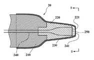
図1−7を参照して、本発明に基づく耳式体温計の実施例について説明する。図1および図2は、本発明に基づく耳式体温計のプローブ20の構造を示す。プローブ20においては、樹脂製の第1断熱部材210の先端に、挿入時に外耳道の温度に影響を与えない断熱性を有する樹脂製の第2高断熱部材(第2断熱部材)220が慣用の連結手段(例えば、溶着、接着剤、圧入、ネジ結合等)によって接続される。第2高断熱部材220は第1断熱部材210との連結部から先端の面221へと先細りのテーパが付けられる。保護カバー230が第1断熱部材210および第2高断熱部材220を覆う。サーミスタリード細線240が第1断熱部材210および第2高断熱部材220内に埋め込まれ、先端折返し部分241が第2高断熱部材220の面221に露出して張り渡される。サーミスタリード細線240の折返し部分241のほぼ中央に超高速応答サーミスタ(サーミスタ)250が装着される。従来の耳式体温計に用いられるサーミスタ12(図8参照)は直径1mm、長さ2−3mmであるが、一方、本発明の耳式体温計に用いられるサーミスタ250は、例えば、一辺が0.3mmの立方体である。With reference to FIGS. 1-7, the Example of the ear-type thermometer based on this invention is described. 1 and 2 show the structure of an
好ましくは、第2高断熱部材220の面221は、図3に示すように、赤外線をサーミスタ250へ反射する効果を高めるために凹面形状に形成され、また、この凹面221を鏡面仕上げにすると反射効率をより一層上げることができる。 Preferably, the
図4は、本発明に基づく体温計のプローブ20を外耳道1に挿入したときの測定位置を示す。プローブ20の先端形状は、プローブ20の中間部が外耳道入口に密着し、プローブ20の先端と鼓膜2との間の空間をできるだけ小さくするように選定されることが好ましい。 FIG. 4 shows the measurement position when the
サーミスタ250の温度を確定する要因としては、鼓膜2と外耳道1からの赤外線の直接放射によるサーミスタリード線240およびサーミスタ250の温度上昇、外耳道内にある空気の直接熱伝導、外耳道内に挿入されたプローブ20による直接熱伝導がある。外耳道1に挿入されるプローブ20の先端部分は、挿入時に外耳道1の温度に影響を与えない必要がある。第2高断熱部材220および保護カバー230はその影響を少なくしている。 Factors that determine the temperature of the
図5は、熱時定数の定義を説明する図である。熱時定数は、任意の温度T1に保持されているサーミスタ250を、急激に周囲温度T2の雰囲気中に挿入したとき、目標温度T2まで変化するのに要する時間をいう。通常は、温度T1、T2の温度差ΔT(=T2−T1)の63.2%(Y)に達するまでの時間Xをいう。ここで対象としているサーミスタ250は、空気中での熱時定数が1秒以下(好ましくは、0.1秒以下)の超高速応答サーミスタである。 FIG. 5 is a diagram for explaining the definition of the thermal time constant. The thermal time constant refers to the time required to change to the target temperature T2 when the
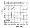
図6は、図1または2に示すプローブ20によって体温を実測したときのサーミスタの温度変化を表すグラフである。縦軸は温度(℃)を、横軸は経過時間(秒)をそれぞれ表す。このとき、プローブ20に実装したサーミスタの熱時定数は1秒であり、温度計測に要する時間は10秒以内である。短時間で計測するためには、空気中でのサーミスタ250の熱時定数が0.1秒程度のものが望ましい。これにより、測定時間を1−2秒に短縮できる。 FIG. 6 is a graph showing the temperature change of the thermistor when the body temperature is actually measured by the
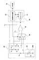
プローブ20の高速応答速度を生かすためには、従来の電子体温計で多く用いられている精度は高いが計測時間のかかるV−F変換方式では実現できない。そこで、本発明の耳式体温計では、例えば、図7に示す測温回路方式を採用する。この測温回路方式では、ADコンバータ31および制御信号処理器32を内蔵するマイクロコントローラ・ユニット(MCU)30を使用する。ADコンバータ内蔵MCUは一般に普及し、10ビットADコンバータ内蔵品までは低価格で選定し易い。VrefはADコンバータ31の基準電源電圧であって、AD変換値のフルスケール値である。MCU内蔵ADコンバータの場合、通常MCUの電源電圧と同じ電圧にする。電源回路40の基準電源電圧Vrefの分路電圧V1、V2、V3は、下記の式(1)、(2)、(3)で表される。R1、R2、R3、R4、Rref、Rthは、電源回路の各抵抗を表す。P1、P2、P3は、アナログスイッチ50の各端子である。
P1:V1=R2/(R1+R2)×Vref (1)
P2:V2=R4/(R3+R4)×Vref (2)
P3:V3=Rth/(Rth+Rref)×Vref (3)
ただし、V2>V3>V1In order to make use of the high-speed response speed of the
P1 : V1 = R2 / (R1 + R2 ) × Vref (1)
P2 : V2 =R4 / (R3 + R4 ) × Vref (2)
P3 : V3 = Rth / (Rth + Rref) × Vref (3)
However, V2 > V3 > V1
誤差要因として、作動増幅器(OP)60のオフセット誤差、作動増幅器60のゲイン誤差(GE)がある。MCU内蔵10ビットADコンバータは逐次比較方式であり誤差としてADオフセット誤差の影響が大きい。アナログスイッチ50を端子P1、P2、P3に切り替えたときのAD変換値をそれぞれA1、A2、A3とする。作動増幅器60の増幅度をNとすると、V1、V2、V3のAD変換値は下記の式(4)、(5)、(6)、(7)で表される。
A1=V1+N×GE×OPオフセット誤差+ADオフセット誤差 (4)
A2=(OPオフセット誤差+V2−V1)×N×GE+ADオフセット誤差 (5)
A3=(OPオフセット誤差+V3−V1)×N×GE+ADオフセット誤差 (6)
A2−A1=(V2−V1)×N×GE (7)As error factors, there are an offset error of the operational amplifier (OP) 60 and a gain error (GE) of the
A1 = V1 + N × GE × OP offset error + AD offset error (4)
A2 = (OP offset error + V2 −V1 ) × N × GE + AD offset error (5)
A3 = (OP offset error + V3 −V1 ) × N × GE + AD offset error (6)
A2 −A1 = (V2 −V1 ) × N × GE (7)
V1、V2、Nは既知であるから、GEを下記の式(8)で求めることができる。
GE=(A2−A1)/N(V2−V1) (8)Since V1 , V2 , and N are known, GE can be obtained by the following equation (8).
GE = (A2 −A1 ) / N (V2 −V1 ) (8)
アナログスイッチ50の端子P1と端子P2におけるAD変換値を読み取る動作を回路校正サイクルと定義すれば、A3−A1=(V3−V1)×N×GEとなる。回路校正サイクルでGEを求めてあるから、作動増幅器(OP)60のゲイン誤差(GE)を除くことができる。温度計測時、MCU30は端子P1と端子P2の校正サイクルを実行し、次に端子P3の計測を行い、計測値から誤差要因を除き、MCU内部テーブルからサーミスタ温度を求めることができる。これを表示器70に体温として表示する。If the operation of reading the AD conversion values at the terminals P1 and P2 of the
本発明の耳式体温計は、人間のみならず、動物にも適用できる。 The ear thermometer of the present invention can be applied not only to humans but also to animals.
1 外耳道 2 鼓膜
10 プローブ 20 プローブ
111 金属ホルダ 116 赤外線吸収膜
210 第1断熱部材 220 第2高断熱部材
221 凹面 230 保護カバー
240 サーミスタリード細線 250 超高速応答サーミスタDESCRIPTION OF SYMBOLS 1 External
Claims (4)
Translated fromJapanesePriority Applications (8)
| Application Number | Priority Date | Filing Date | Title |
|---|---|---|---|
| JP2005071350AJP4214124B2 (en) | 2005-03-14 | 2005-03-14 | Ear thermometer |
| DE602006004905TDE602006004905D1 (en) | 2005-03-14 | 2006-03-07 | Ear thermometer |
| AT06004624TATE421680T1 (en) | 2005-03-14 | 2006-03-07 | EAR FEVER THERMOMETER |
| EP06004624AEP1703267B1 (en) | 2005-03-14 | 2006-03-07 | Ear-type clinical thermometer |
| ES06004624TES2319223T3 (en) | 2005-03-14 | 2006-03-07 | CLINICAL AUTICULAR THERMOMETER. |
| US11/375,554US7410290B2 (en) | 2005-03-14 | 2006-03-13 | Ear-type clinical thermometer |
| CN2006100678509ACN1862241B (en) | 2005-03-14 | 2006-03-14 | Ear-type clinical thermometer |
| HK07103247.8AHK1096148B (en) | 2005-03-14 | 2007-03-27 | Ear-type clinical thermometer |
Applications Claiming Priority (1)
| Application Number | Priority Date | Filing Date | Title |
|---|---|---|---|
| JP2005071350AJP4214124B2 (en) | 2005-03-14 | 2005-03-14 | Ear thermometer |
Publications (2)
| Publication Number | Publication Date |
|---|---|
| JP2006250883A JP2006250883A (en) | 2006-09-21 |
| JP4214124B2true JP4214124B2 (en) | 2009-01-28 |
Family
ID=36649073
Family Applications (1)
| Application Number | Title | Priority Date | Filing Date |
|---|---|---|---|
| JP2005071350AExpired - LifetimeJP4214124B2 (en) | 2005-03-14 | 2005-03-14 | Ear thermometer |
Country Status (7)
| Country | Link |
|---|---|
| US (1) | US7410290B2 (en) |
| EP (1) | EP1703267B1 (en) |
| JP (1) | JP4214124B2 (en) |
| CN (1) | CN1862241B (en) |
| AT (1) | ATE421680T1 (en) |
| DE (1) | DE602006004905D1 (en) |
| ES (1) | ES2319223T3 (en) |
Families Citing this family (367)
| Publication number | Priority date | Publication date | Assignee | Title |
|---|---|---|---|---|
| DE102007002369B3 (en)* | 2007-01-17 | 2008-05-15 | Drägerwerk AG & Co. KGaA | Dual temperature sensor for e.g. patient, has sensor units with connections arranged parallel to each other in block and at distance to each other from external surface of block, where distance is formed by layer of insulating material |
| ES2480297T3 (en) | 2007-06-12 | 2014-07-25 | Bio Echo Net Inc | Auricular thermometer and measuring device used with it |
| US8303173B2 (en)* | 2007-10-29 | 2012-11-06 | Smiths Medical Asd, Inc. | Dual potting temperature probe |
| JP5564165B2 (en)* | 2008-04-21 | 2014-07-30 | 株式会社バイオエコーネット | Ear-type continuous body temperature measuring device |
| US10378106B2 (en) | 2008-11-14 | 2019-08-13 | Asm Ip Holding B.V. | Method of forming insulation film by modified PEALD |
| US9394608B2 (en) | 2009-04-06 | 2016-07-19 | Asm America, Inc. | Semiconductor processing reactor and components thereof |
| US8186876B2 (en)* | 2009-04-20 | 2012-05-29 | Welch Allyn, Inc. | Calibrated assembly for IR thermometer apparatus |
| US8136985B2 (en)* | 2009-05-05 | 2012-03-20 | Welch Allyn, Inc. | IR thermometer thermal isolation tip assembly |
| US9297705B2 (en) | 2009-05-06 | 2016-03-29 | Asm America, Inc. | Smart temperature measuring device |
| US8382370B2 (en)* | 2009-05-06 | 2013-02-26 | Asm America, Inc. | Thermocouple assembly with guarded thermocouple junction |
| US8802201B2 (en) | 2009-08-14 | 2014-08-12 | Asm America, Inc. | Systems and methods for thin-film deposition of metal oxides using excited nitrogen-oxygen species |
| US9312155B2 (en) | 2011-06-06 | 2016-04-12 | Asm Japan K.K. | High-throughput semiconductor-processing apparatus equipped with multiple dual-chamber modules |
| US10364496B2 (en) | 2011-06-27 | 2019-07-30 | Asm Ip Holding B.V. | Dual section module having shared and unshared mass flow controllers |
| US10854498B2 (en) | 2011-07-15 | 2020-12-01 | Asm Ip Holding B.V. | Wafer-supporting device and method for producing same |
| US20130023129A1 (en) | 2011-07-20 | 2013-01-24 | Asm America, Inc. | Pressure transmitter for a semiconductor processing environment |
| US9017481B1 (en) | 2011-10-28 | 2015-04-28 | Asm America, Inc. | Process feed management for semiconductor substrate processing |
| US8899828B2 (en)* | 2012-03-22 | 2014-12-02 | Texas Instruments Incorporated | Heat sensor correction |
| US9659799B2 (en) | 2012-08-28 | 2017-05-23 | Asm Ip Holding B.V. | Systems and methods for dynamic semiconductor process scheduling |
| US10714315B2 (en) | 2012-10-12 | 2020-07-14 | Asm Ip Holdings B.V. | Semiconductor reaction chamber showerhead |
| CN102961124B (en)* | 2012-11-05 | 2015-04-15 | 东莞市嵘丰医疗器械有限公司 | Thermosensitive forehead temperature gun, forehead temperature measuring method and operating method of thermosensitive forehead temperature gun |
| US20160376700A1 (en) | 2013-02-01 | 2016-12-29 | Asm Ip Holding B.V. | System for treatment of deposition reactor |
| US9484191B2 (en) | 2013-03-08 | 2016-11-01 | Asm Ip Holding B.V. | Pulsed remote plasma method and system |
| US9589770B2 (en) | 2013-03-08 | 2017-03-07 | Asm Ip Holding B.V. | Method and systems for in-situ formation of intermediate reactive species |
| US9240412B2 (en) | 2013-09-27 | 2016-01-19 | Asm Ip Holding B.V. | Semiconductor structure and device and methods of forming same using selective epitaxial process |
| US10683571B2 (en) | 2014-02-25 | 2020-06-16 | Asm Ip Holding B.V. | Gas supply manifold and method of supplying gases to chamber using same |
| US10167557B2 (en) | 2014-03-18 | 2019-01-01 | Asm Ip Holding B.V. | Gas distribution system, reactor including the system, and methods of using the same |
| US11015245B2 (en) | 2014-03-19 | 2021-05-25 | Asm Ip Holding B.V. | Gas-phase reactor and system having exhaust plenum and components thereof |
| US10858737B2 (en) | 2014-07-28 | 2020-12-08 | Asm Ip Holding B.V. | Showerhead assembly and components thereof |
| US9890456B2 (en) | 2014-08-21 | 2018-02-13 | Asm Ip Holding B.V. | Method and system for in situ formation of gas-phase compounds |
| US10941490B2 (en) | 2014-10-07 | 2021-03-09 | Asm Ip Holding B.V. | Multiple temperature range susceptor, assembly, reactor and system including the susceptor, and methods of using the same |
| US9657845B2 (en) | 2014-10-07 | 2017-05-23 | Asm Ip Holding B.V. | Variable conductance gas distribution apparatus and method |
| KR102263121B1 (en) | 2014-12-22 | 2021-06-09 | 에이에스엠 아이피 홀딩 비.브이. | Semiconductor device and manufacuring method thereof |
| US10529542B2 (en) | 2015-03-11 | 2020-01-07 | Asm Ip Holdings B.V. | Cross-flow reactor and method |
| US10276355B2 (en) | 2015-03-12 | 2019-04-30 | Asm Ip Holding B.V. | Multi-zone reactor, system including the reactor, and method of using the same |
| US10458018B2 (en) | 2015-06-26 | 2019-10-29 | Asm Ip Holding B.V. | Structures including metal carbide material, devices including the structures, and methods of forming same |
| US10600673B2 (en) | 2015-07-07 | 2020-03-24 | Asm Ip Holding B.V. | Magnetic susceptor to baseplate seal |
| US9960072B2 (en) | 2015-09-29 | 2018-05-01 | Asm Ip Holding B.V. | Variable adjustment for precise matching of multiple chamber cavity housings |
| US10211308B2 (en) | 2015-10-21 | 2019-02-19 | Asm Ip Holding B.V. | NbMC layers |
| US10322384B2 (en) | 2015-11-09 | 2019-06-18 | Asm Ip Holding B.V. | Counter flow mixer for process chamber |
| US11139308B2 (en) | 2015-12-29 | 2021-10-05 | Asm Ip Holding B.V. | Atomic layer deposition of III-V compounds to form V-NAND devices |
| US10468251B2 (en) | 2016-02-19 | 2019-11-05 | Asm Ip Holding B.V. | Method for forming spacers using silicon nitride film for spacer-defined multiple patterning |
| US10529554B2 (en) | 2016-02-19 | 2020-01-07 | Asm Ip Holding B.V. | Method for forming silicon nitride film selectively on sidewalls or flat surfaces of trenches |
| US10501866B2 (en) | 2016-03-09 | 2019-12-10 | Asm Ip Holding B.V. | Gas distribution apparatus for improved film uniformity in an epitaxial system |
| US10343920B2 (en) | 2016-03-18 | 2019-07-09 | Asm Ip Holding B.V. | Aligned carbon nanotubes |
| US9892913B2 (en) | 2016-03-24 | 2018-02-13 | Asm Ip Holding B.V. | Radial and thickness control via biased multi-port injection settings |
| US10190213B2 (en) | 2016-04-21 | 2019-01-29 | Asm Ip Holding B.V. | Deposition of metal borides |
| US10865475B2 (en) | 2016-04-21 | 2020-12-15 | Asm Ip Holding B.V. | Deposition of metal borides and silicides |
| US10032628B2 (en) | 2016-05-02 | 2018-07-24 | Asm Ip Holding B.V. | Source/drain performance through conformal solid state doping |
| US10367080B2 (en) | 2016-05-02 | 2019-07-30 | Asm Ip Holding B.V. | Method of forming a germanium oxynitride film |
| KR102592471B1 (en) | 2016-05-17 | 2023-10-20 | 에이에스엠 아이피 홀딩 비.브이. | Method of forming metal interconnection and method of fabricating semiconductor device using the same |
| GB2554632B (en)* | 2016-05-24 | 2021-02-24 | Inova Design Solution Ltd | Portable physiology monitor |
| US11453943B2 (en) | 2016-05-25 | 2022-09-27 | Asm Ip Holding B.V. | Method for forming carbon-containing silicon/metal oxide or nitride film by ALD using silicon precursor and hydrocarbon precursor |
| CN107543614A (en)* | 2016-06-24 | 2018-01-05 | 上海新微技术研发中心有限公司 | Thermopile sensor |
| US10388509B2 (en) | 2016-06-28 | 2019-08-20 | Asm Ip Holding B.V. | Formation of epitaxial layers via dislocation filtering |
| US9859151B1 (en) | 2016-07-08 | 2018-01-02 | Asm Ip Holding B.V. | Selective film deposition method to form air gaps |
| US10612137B2 (en) | 2016-07-08 | 2020-04-07 | Asm Ip Holdings B.V. | Organic reactants for atomic layer deposition |
| US10714385B2 (en) | 2016-07-19 | 2020-07-14 | Asm Ip Holding B.V. | Selective deposition of tungsten |
| KR102354490B1 (en) | 2016-07-27 | 2022-01-21 | 에이에스엠 아이피 홀딩 비.브이. | Method of processing a substrate |
| US9812320B1 (en) | 2016-07-28 | 2017-11-07 | Asm Ip Holding B.V. | Method and apparatus for filling a gap |
| KR102532607B1 (en) | 2016-07-28 | 2023-05-15 | 에이에스엠 아이피 홀딩 비.브이. | Substrate processing apparatus and method of operating the same |
| US9887082B1 (en) | 2016-07-28 | 2018-02-06 | Asm Ip Holding B.V. | Method and apparatus for filling a gap |
| US10395919B2 (en) | 2016-07-28 | 2019-08-27 | Asm Ip Holding B.V. | Method and apparatus for filling a gap |
| KR102613349B1 (en) | 2016-08-25 | 2023-12-14 | 에이에스엠 아이피 홀딩 비.브이. | Exhaust apparatus and substrate processing apparatus and thin film fabricating method using the same |
| US10410943B2 (en) | 2016-10-13 | 2019-09-10 | Asm Ip Holding B.V. | Method for passivating a surface of a semiconductor and related systems |
| US10643826B2 (en) | 2016-10-26 | 2020-05-05 | Asm Ip Holdings B.V. | Methods for thermally calibrating reaction chambers |
| US11532757B2 (en) | 2016-10-27 | 2022-12-20 | Asm Ip Holding B.V. | Deposition of charge trapping layers |
| US10435790B2 (en) | 2016-11-01 | 2019-10-08 | Asm Ip Holding B.V. | Method of subatmospheric plasma-enhanced ALD using capacitively coupled electrodes with narrow gap |
| US10229833B2 (en) | 2016-11-01 | 2019-03-12 | Asm Ip Holding B.V. | Methods for forming a transition metal nitride film on a substrate by atomic layer deposition and related semiconductor device structures |
| US10643904B2 (en) | 2016-11-01 | 2020-05-05 | Asm Ip Holdings B.V. | Methods for forming a semiconductor device and related semiconductor device structures |
| US10714350B2 (en) | 2016-11-01 | 2020-07-14 | ASM IP Holdings, B.V. | Methods for forming a transition metal niobium nitride film on a substrate by atomic layer deposition and related semiconductor device structures |
| US10134757B2 (en) | 2016-11-07 | 2018-11-20 | Asm Ip Holding B.V. | Method of processing a substrate and a device manufactured by using the method |
| KR102546317B1 (en) | 2016-11-15 | 2023-06-21 | 에이에스엠 아이피 홀딩 비.브이. | Gas supply unit and substrate processing apparatus including the same |
| US10340135B2 (en) | 2016-11-28 | 2019-07-02 | Asm Ip Holding B.V. | Method of topologically restricted plasma-enhanced cyclic deposition of silicon or metal nitride |
| KR102762543B1 (en) | 2016-12-14 | 2025-02-05 | 에이에스엠 아이피 홀딩 비.브이. | Substrate processing apparatus |
| US11447861B2 (en) | 2016-12-15 | 2022-09-20 | Asm Ip Holding B.V. | Sequential infiltration synthesis apparatus and a method of forming a patterned structure |
| US11581186B2 (en) | 2016-12-15 | 2023-02-14 | Asm Ip Holding B.V. | Sequential infiltration synthesis apparatus |
| KR102700194B1 (en) | 2016-12-19 | 2024-08-28 | 에이에스엠 아이피 홀딩 비.브이. | Substrate processing apparatus |
| US10269558B2 (en) | 2016-12-22 | 2019-04-23 | Asm Ip Holding B.V. | Method of forming a structure on a substrate |
| US10867788B2 (en) | 2016-12-28 | 2020-12-15 | Asm Ip Holding B.V. | Method of forming a structure on a substrate |
| US11390950B2 (en) | 2017-01-10 | 2022-07-19 | Asm Ip Holding B.V. | Reactor system and method to reduce residue buildup during a film deposition process |
| US10655221B2 (en) | 2017-02-09 | 2020-05-19 | Asm Ip Holding B.V. | Method for depositing oxide film by thermal ALD and PEALD |
| US10468261B2 (en) | 2017-02-15 | 2019-11-05 | Asm Ip Holding B.V. | Methods for forming a metallic film on a substrate by cyclical deposition and related semiconductor device structures |
| US10529563B2 (en) | 2017-03-29 | 2020-01-07 | Asm Ip Holdings B.V. | Method for forming doped metal oxide films on a substrate by cyclical deposition and related semiconductor device structures |
| US10283353B2 (en) | 2017-03-29 | 2019-05-07 | Asm Ip Holding B.V. | Method of reforming insulating film deposited on substrate with recess pattern |
| KR102457289B1 (en) | 2017-04-25 | 2022-10-21 | 에이에스엠 아이피 홀딩 비.브이. | Method for depositing a thin film and manufacturing a semiconductor device |
| US10892156B2 (en) | 2017-05-08 | 2021-01-12 | Asm Ip Holding B.V. | Methods for forming a silicon nitride film on a substrate and related semiconductor device structures |
| US10446393B2 (en) | 2017-05-08 | 2019-10-15 | Asm Ip Holding B.V. | Methods for forming silicon-containing epitaxial layers and related semiconductor device structures |
| US10770286B2 (en) | 2017-05-08 | 2020-09-08 | Asm Ip Holdings B.V. | Methods for selectively forming a silicon nitride film on a substrate and related semiconductor device structures |
| US10504742B2 (en) | 2017-05-31 | 2019-12-10 | Asm Ip Holding B.V. | Method of atomic layer etching using hydrogen plasma |
| US10886123B2 (en) | 2017-06-02 | 2021-01-05 | Asm Ip Holding B.V. | Methods for forming low temperature semiconductor layers and related semiconductor device structures |
| US12040200B2 (en) | 2017-06-20 | 2024-07-16 | Asm Ip Holding B.V. | Semiconductor processing apparatus and methods for calibrating a semiconductor processing apparatus |
| US11306395B2 (en) | 2017-06-28 | 2022-04-19 | Asm Ip Holding B.V. | Methods for depositing a transition metal nitride film on a substrate by atomic layer deposition and related deposition apparatus |
| US10685834B2 (en) | 2017-07-05 | 2020-06-16 | Asm Ip Holdings B.V. | Methods for forming a silicon germanium tin layer and related semiconductor device structures |
| KR20190009245A (en) | 2017-07-18 | 2019-01-28 | 에이에스엠 아이피 홀딩 비.브이. | Methods for forming a semiconductor device structure and related semiconductor device structures |
| US11018002B2 (en) | 2017-07-19 | 2021-05-25 | Asm Ip Holding B.V. | Method for selectively depositing a Group IV semiconductor and related semiconductor device structures |
| US11374112B2 (en) | 2017-07-19 | 2022-06-28 | Asm Ip Holding B.V. | Method for depositing a group IV semiconductor and related semiconductor device structures |
| US10541333B2 (en) | 2017-07-19 | 2020-01-21 | Asm Ip Holding B.V. | Method for depositing a group IV semiconductor and related semiconductor device structures |
| US10312055B2 (en) | 2017-07-26 | 2019-06-04 | Asm Ip Holding B.V. | Method of depositing film by PEALD using negative bias |
| US10605530B2 (en) | 2017-07-26 | 2020-03-31 | Asm Ip Holding B.V. | Assembly of a liner and a flange for a vertical furnace as well as the liner and the vertical furnace |
| US10590535B2 (en) | 2017-07-26 | 2020-03-17 | Asm Ip Holdings B.V. | Chemical treatment, deposition and/or infiltration apparatus and method for using the same |
| TWI815813B (en) | 2017-08-04 | 2023-09-21 | 荷蘭商Asm智慧財產控股公司 | Showerhead assembly for distributing a gas within a reaction chamber |
| US10770336B2 (en) | 2017-08-08 | 2020-09-08 | Asm Ip Holding B.V. | Substrate lift mechanism and reactor including same |
| US10692741B2 (en) | 2017-08-08 | 2020-06-23 | Asm Ip Holdings B.V. | Radiation shield |
| US11769682B2 (en) | 2017-08-09 | 2023-09-26 | Asm Ip Holding B.V. | Storage apparatus for storing cassettes for substrates and processing apparatus equipped therewith |
| US10249524B2 (en) | 2017-08-09 | 2019-04-02 | Asm Ip Holding B.V. | Cassette holder assembly for a substrate cassette and holding member for use in such assembly |
| US11139191B2 (en) | 2017-08-09 | 2021-10-05 | Asm Ip Holding B.V. | Storage apparatus for storing cassettes for substrates and processing apparatus equipped therewith |
| USD900036S1 (en) | 2017-08-24 | 2020-10-27 | Asm Ip Holding B.V. | Heater electrical connector and adapter |
| US11830730B2 (en) | 2017-08-29 | 2023-11-28 | Asm Ip Holding B.V. | Layer forming method and apparatus |
| US11056344B2 (en) | 2017-08-30 | 2021-07-06 | Asm Ip Holding B.V. | Layer forming method |
| US11295980B2 (en) | 2017-08-30 | 2022-04-05 | Asm Ip Holding B.V. | Methods for depositing a molybdenum metal film over a dielectric surface of a substrate by a cyclical deposition process and related semiconductor device structures |
| KR102491945B1 (en) | 2017-08-30 | 2023-01-26 | 에이에스엠 아이피 홀딩 비.브이. | Substrate processing apparatus |
| KR102401446B1 (en) | 2017-08-31 | 2022-05-24 | 에이에스엠 아이피 홀딩 비.브이. | Substrate processing apparatus |
| US10607895B2 (en) | 2017-09-18 | 2020-03-31 | Asm Ip Holdings B.V. | Method for forming a semiconductor device structure comprising a gate fill metal |
| KR102630301B1 (en) | 2017-09-21 | 2024-01-29 | 에이에스엠 아이피 홀딩 비.브이. | Method of sequential infiltration synthesis treatment of infiltrateable material and structures and devices formed using same |
| US10844484B2 (en) | 2017-09-22 | 2020-11-24 | Asm Ip Holding B.V. | Apparatus for dispensing a vapor phase reactant to a reaction chamber and related methods |
| US10658205B2 (en) | 2017-09-28 | 2020-05-19 | Asm Ip Holdings B.V. | Chemical dispensing apparatus and methods for dispensing a chemical to a reaction chamber |
| US10403504B2 (en) | 2017-10-05 | 2019-09-03 | Asm Ip Holding B.V. | Method for selectively depositing a metallic film on a substrate |
| US10319588B2 (en) | 2017-10-10 | 2019-06-11 | Asm Ip Holding B.V. | Method for depositing a metal chalcogenide on a substrate by cyclical deposition |
| US11213252B2 (en) | 2017-10-20 | 2022-01-04 | Starkey Laboratories, Inc. | Devices and sensing methods for measuring temperature from an ear |
| US10923344B2 (en) | 2017-10-30 | 2021-02-16 | Asm Ip Holding B.V. | Methods for forming a semiconductor structure and related semiconductor structures |
| US10529219B2 (en) | 2017-11-10 | 2020-01-07 | Ecolab Usa Inc. | Hand hygiene compliance monitoring |
| US10910262B2 (en) | 2017-11-16 | 2021-02-02 | Asm Ip Holding B.V. | Method of selectively depositing a capping layer structure on a semiconductor device structure |
| KR102443047B1 (en) | 2017-11-16 | 2022-09-14 | 에이에스엠 아이피 홀딩 비.브이. | Method of processing a substrate and a device manufactured by the same |
| US11022879B2 (en) | 2017-11-24 | 2021-06-01 | Asm Ip Holding B.V. | Method of forming an enhanced unexposed photoresist layer |
| WO2019103613A1 (en) | 2017-11-27 | 2019-05-31 | Asm Ip Holding B.V. | A storage device for storing wafer cassettes for use with a batch furnace |
| CN111344522B (en) | 2017-11-27 | 2022-04-12 | 阿斯莫Ip控股公司 | Including clean mini-environment device |
| US10290508B1 (en) | 2017-12-05 | 2019-05-14 | Asm Ip Holding B.V. | Method for forming vertical spacers for spacer-defined patterning |
| US10872771B2 (en) | 2018-01-16 | 2020-12-22 | Asm Ip Holding B. V. | Method for depositing a material film on a substrate within a reaction chamber by a cyclical deposition process and related device structures |
| TWI799494B (en) | 2018-01-19 | 2023-04-21 | 荷蘭商Asm 智慧財產控股公司 | Deposition method |
| KR102695659B1 (en) | 2018-01-19 | 2024-08-14 | 에이에스엠 아이피 홀딩 비.브이. | Method for depositing a gap filling layer by plasma assisted deposition |
| USD903477S1 (en) | 2018-01-24 | 2020-12-01 | Asm Ip Holdings B.V. | Metal clamp |
| US11018047B2 (en) | 2018-01-25 | 2021-05-25 | Asm Ip Holding B.V. | Hybrid lift pin |
| US10535516B2 (en) | 2018-02-01 | 2020-01-14 | Asm Ip Holdings B.V. | Method for depositing a semiconductor structure on a surface of a substrate and related semiconductor structures |
| USD880437S1 (en) | 2018-02-01 | 2020-04-07 | Asm Ip Holding B.V. | Gas supply plate for semiconductor manufacturing apparatus |
| US11081345B2 (en) | 2018-02-06 | 2021-08-03 | Asm Ip Holding B.V. | Method of post-deposition treatment for silicon oxide film |
| WO2019158960A1 (en) | 2018-02-14 | 2019-08-22 | Asm Ip Holding B.V. | A method for depositing a ruthenium-containing film on a substrate by a cyclical deposition process |
| US10896820B2 (en) | 2018-02-14 | 2021-01-19 | Asm Ip Holding B.V. | Method for depositing a ruthenium-containing film on a substrate by a cyclical deposition process |
| US10731249B2 (en) | 2018-02-15 | 2020-08-04 | Asm Ip Holding B.V. | Method of forming a transition metal containing film on a substrate by a cyclical deposition process, a method for supplying a transition metal halide compound to a reaction chamber, and related vapor deposition apparatus |
| KR102636427B1 (en) | 2018-02-20 | 2024-02-13 | 에이에스엠 아이피 홀딩 비.브이. | Substrate processing method and apparatus |
| US10658181B2 (en) | 2018-02-20 | 2020-05-19 | Asm Ip Holding B.V. | Method of spacer-defined direct patterning in semiconductor fabrication |
| US10975470B2 (en) | 2018-02-23 | 2021-04-13 | Asm Ip Holding B.V. | Apparatus for detecting or monitoring for a chemical precursor in a high temperature environment |
| US11473195B2 (en) | 2018-03-01 | 2022-10-18 | Asm Ip Holding B.V. | Semiconductor processing apparatus and a method for processing a substrate |
| US11629406B2 (en) | 2018-03-09 | 2023-04-18 | Asm Ip Holding B.V. | Semiconductor processing apparatus comprising one or more pyrometers for measuring a temperature of a substrate during transfer of the substrate |
| US11114283B2 (en) | 2018-03-16 | 2021-09-07 | Asm Ip Holding B.V. | Reactor, system including the reactor, and methods of manufacturing and using same |
| KR102646467B1 (en) | 2018-03-27 | 2024-03-11 | 에이에스엠 아이피 홀딩 비.브이. | Method of forming an electrode on a substrate and a semiconductor device structure including an electrode |
| US10510536B2 (en) | 2018-03-29 | 2019-12-17 | Asm Ip Holding B.V. | Method of depositing a co-doped polysilicon film on a surface of a substrate within a reaction chamber |
| US11088002B2 (en) | 2018-03-29 | 2021-08-10 | Asm Ip Holding B.V. | Substrate rack and a substrate processing system and method |
| US11230766B2 (en) | 2018-03-29 | 2022-01-25 | Asm Ip Holding B.V. | Substrate processing apparatus and method |
| KR102501472B1 (en) | 2018-03-30 | 2023-02-20 | 에이에스엠 아이피 홀딩 비.브이. | Substrate processing method |
| KR102600229B1 (en) | 2018-04-09 | 2023-11-10 | 에이에스엠 아이피 홀딩 비.브이. | Substrate supporting device, substrate processing apparatus including the same and substrate processing method |
| US12025484B2 (en) | 2018-05-08 | 2024-07-02 | Asm Ip Holding B.V. | Thin film forming method |
| TWI811348B (en) | 2018-05-08 | 2023-08-11 | 荷蘭商Asm 智慧財產控股公司 | Methods for depositing an oxide film on a substrate by a cyclical deposition process and related device structures |
| US12272527B2 (en) | 2018-05-09 | 2025-04-08 | Asm Ip Holding B.V. | Apparatus for use with hydrogen radicals and method of using same |
| KR20190129718A (en) | 2018-05-11 | 2019-11-20 | 에이에스엠 아이피 홀딩 비.브이. | Methods for forming a doped metal carbide film on a substrate and related semiconductor device structures |
| KR102596988B1 (en) | 2018-05-28 | 2023-10-31 | 에이에스엠 아이피 홀딩 비.브이. | Method of processing a substrate and a device manufactured by the same |
| US11718913B2 (en) | 2018-06-04 | 2023-08-08 | Asm Ip Holding B.V. | Gas distribution system and reactor system including same |
| TWI840362B (en) | 2018-06-04 | 2024-05-01 | 荷蘭商Asm Ip私人控股有限公司 | Wafer handling chamber with moisture reduction |
| US11286562B2 (en) | 2018-06-08 | 2022-03-29 | Asm Ip Holding B.V. | Gas-phase chemical reactor and method of using same |
| KR102568797B1 (en) | 2018-06-21 | 2023-08-21 | 에이에스엠 아이피 홀딩 비.브이. | Substrate processing system |
| US10797133B2 (en) | 2018-06-21 | 2020-10-06 | Asm Ip Holding B.V. | Method for depositing a phosphorus doped silicon arsenide film and related semiconductor device structures |
| KR102854019B1 (en) | 2018-06-27 | 2025-09-02 | 에이에스엠 아이피 홀딩 비.브이. | Periodic deposition method for forming a metal-containing material and films and structures comprising the metal-containing material |
| TWI873894B (en) | 2018-06-27 | 2025-02-21 | 荷蘭商Asm Ip私人控股有限公司 | Cyclic deposition methods for forming metal-containing material and films and structures including the metal-containing material |
| US10612136B2 (en) | 2018-06-29 | 2020-04-07 | ASM IP Holding, B.V. | Temperature-controlled flange and reactor system including same |
| KR102686758B1 (en) | 2018-06-29 | 2024-07-18 | 에이에스엠 아이피 홀딩 비.브이. | Method for depositing a thin film and manufacturing a semiconductor device |
| US10388513B1 (en) | 2018-07-03 | 2019-08-20 | Asm Ip Holding B.V. | Method for depositing silicon-free carbon-containing film as gap-fill layer by pulse plasma-assisted deposition |
| US10755922B2 (en) | 2018-07-03 | 2020-08-25 | Asm Ip Holding B.V. | Method for depositing silicon-free carbon-containing film as gap-fill layer by pulse plasma-assisted deposition |
| US10767789B2 (en) | 2018-07-16 | 2020-09-08 | Asm Ip Holding B.V. | Diaphragm valves, valve components, and methods for forming valve components |
| US10483099B1 (en) | 2018-07-26 | 2019-11-19 | Asm Ip Holding B.V. | Method for forming thermally stable organosilicon polymer film |
| US11053591B2 (en) | 2018-08-06 | 2021-07-06 | Asm Ip Holding B.V. | Multi-port gas injection system and reactor system including same |
| US10883175B2 (en) | 2018-08-09 | 2021-01-05 | Asm Ip Holding B.V. | Vertical furnace for processing substrates and a liner for use therein |
| US10829852B2 (en) | 2018-08-16 | 2020-11-10 | Asm Ip Holding B.V. | Gas distribution device for a wafer processing apparatus |
| US11430674B2 (en) | 2018-08-22 | 2022-08-30 | Asm Ip Holding B.V. | Sensor array, apparatus for dispensing a vapor phase reactant to a reaction chamber and related methods |
| US11024523B2 (en) | 2018-09-11 | 2021-06-01 | Asm Ip Holding B.V. | Substrate processing apparatus and method |
| KR102707956B1 (en) | 2018-09-11 | 2024-09-19 | 에이에스엠 아이피 홀딩 비.브이. | Method for deposition of a thin film |
| US11049751B2 (en) | 2018-09-14 | 2021-06-29 | Asm Ip Holding B.V. | Cassette supply system to store and handle cassettes and processing apparatus equipped therewith |
| CN110970344B (en) | 2018-10-01 | 2024-10-25 | Asmip控股有限公司 | Substrate holding apparatus, system comprising the same and method of using the same |
| US11232963B2 (en) | 2018-10-03 | 2022-01-25 | Asm Ip Holding B.V. | Substrate processing apparatus and method |
| KR102592699B1 (en) | 2018-10-08 | 2023-10-23 | 에이에스엠 아이피 홀딩 비.브이. | Substrate support unit and apparatuses for depositing thin film and processing the substrate including the same |
| US10847365B2 (en) | 2018-10-11 | 2020-11-24 | Asm Ip Holding B.V. | Method of forming conformal silicon carbide film by cyclic CVD |
| US10811256B2 (en) | 2018-10-16 | 2020-10-20 | Asm Ip Holding B.V. | Method for etching a carbon-containing feature |
| KR102546322B1 (en) | 2018-10-19 | 2023-06-21 | 에이에스엠 아이피 홀딩 비.브이. | Substrate processing apparatus and substrate processing method |
| KR102605121B1 (en) | 2018-10-19 | 2023-11-23 | 에이에스엠 아이피 홀딩 비.브이. | Substrate processing apparatus and substrate processing method |
| USD948463S1 (en) | 2018-10-24 | 2022-04-12 | Asm Ip Holding B.V. | Susceptor for semiconductor substrate supporting apparatus |
| US10381219B1 (en) | 2018-10-25 | 2019-08-13 | Asm Ip Holding B.V. | Methods for forming a silicon nitride film |
| US12378665B2 (en) | 2018-10-26 | 2025-08-05 | Asm Ip Holding B.V. | High temperature coatings for a preclean and etch apparatus and related methods |
| US11087997B2 (en) | 2018-10-31 | 2021-08-10 | Asm Ip Holding B.V. | Substrate processing apparatus for processing substrates |
| KR102748291B1 (en) | 2018-11-02 | 2024-12-31 | 에이에스엠 아이피 홀딩 비.브이. | Substrate support unit and substrate processing apparatus including the same |
| US11572620B2 (en) | 2018-11-06 | 2023-02-07 | Asm Ip Holding B.V. | Methods for selectively depositing an amorphous silicon film on a substrate |
| US11031242B2 (en) | 2018-11-07 | 2021-06-08 | Asm Ip Holding B.V. | Methods for depositing a boron doped silicon germanium film |
| US10847366B2 (en) | 2018-11-16 | 2020-11-24 | Asm Ip Holding B.V. | Methods for depositing a transition metal chalcogenide film on a substrate by a cyclical deposition process |
| US10818758B2 (en) | 2018-11-16 | 2020-10-27 | Asm Ip Holding B.V. | Methods for forming a metal silicate film on a substrate in a reaction chamber and related semiconductor device structures |
| US10559458B1 (en) | 2018-11-26 | 2020-02-11 | Asm Ip Holding B.V. | Method of forming oxynitride film |
| US12040199B2 (en) | 2018-11-28 | 2024-07-16 | Asm Ip Holding B.V. | Substrate processing apparatus for processing substrates |
| US11217444B2 (en) | 2018-11-30 | 2022-01-04 | Asm Ip Holding B.V. | Method for forming an ultraviolet radiation responsive metal oxide-containing film |
| KR102636428B1 (en) | 2018-12-04 | 2024-02-13 | 에이에스엠 아이피 홀딩 비.브이. | A method for cleaning a substrate processing apparatus |
| US11158513B2 (en) | 2018-12-13 | 2021-10-26 | Asm Ip Holding B.V. | Methods for forming a rhenium-containing film on a substrate by a cyclical deposition process and related semiconductor device structures |
| TWI874340B (en) | 2018-12-14 | 2025-03-01 | 荷蘭商Asm Ip私人控股有限公司 | Method of forming device structure, structure formed by the method and system for performing the method |
| TWI866480B (en) | 2019-01-17 | 2024-12-11 | 荷蘭商Asm Ip 私人控股有限公司 | Methods of forming a transition metal containing film on a substrate by a cyclical deposition process |
| KR102727227B1 (en) | 2019-01-22 | 2024-11-07 | 에이에스엠 아이피 홀딩 비.브이. | Semiconductor processing device |
| CN111524788B (en) | 2019-02-01 | 2023-11-24 | Asm Ip私人控股有限公司 | Method for forming topologically selective films of silicon oxide |
| TWI845607B (en) | 2019-02-20 | 2024-06-21 | 荷蘭商Asm Ip私人控股有限公司 | Cyclical deposition method and apparatus for filling a recess formed within a substrate surface |
| TWI838458B (en) | 2019-02-20 | 2024-04-11 | 荷蘭商Asm Ip私人控股有限公司 | Apparatus and methods for plug fill deposition in 3-d nand applications |
| KR102626263B1 (en) | 2019-02-20 | 2024-01-16 | 에이에스엠 아이피 홀딩 비.브이. | Cyclical deposition method including treatment step and apparatus for same |
| TWI873122B (en) | 2019-02-20 | 2025-02-21 | 荷蘭商Asm Ip私人控股有限公司 | Method of filling a recess formed within a surface of a substrate, semiconductor structure formed according to the method, and semiconductor processing apparatus |
| TWI842826B (en) | 2019-02-22 | 2024-05-21 | 荷蘭商Asm Ip私人控股有限公司 | Substrate processing apparatus and method for processing substrate |
| KR102782593B1 (en) | 2019-03-08 | 2025-03-14 | 에이에스엠 아이피 홀딩 비.브이. | Structure Including SiOC Layer and Method of Forming Same |
| KR102858005B1 (en) | 2019-03-08 | 2025-09-09 | 에이에스엠 아이피 홀딩 비.브이. | Method for Selective Deposition of Silicon Nitride Layer and Structure Including Selectively-Deposited Silicon Nitride Layer |
| US11742198B2 (en) | 2019-03-08 | 2023-08-29 | Asm Ip Holding B.V. | Structure including SiOCN layer and method of forming same |
| JP2020167398A (en) | 2019-03-28 | 2020-10-08 | エーエスエム・アイピー・ホールディング・ベー・フェー | Door openers and substrate processing equipment provided with door openers |
| KR102809999B1 (en) | 2019-04-01 | 2025-05-19 | 에이에스엠 아이피 홀딩 비.브이. | Method of manufacturing semiconductor device |
| KR20200123380A (en) | 2019-04-19 | 2020-10-29 | 에이에스엠 아이피 홀딩 비.브이. | Layer forming method and apparatus |
| KR20200125453A (en) | 2019-04-24 | 2020-11-04 | 에이에스엠 아이피 홀딩 비.브이. | Gas-phase reactor system and method of using same |
| KR20200130121A (en) | 2019-05-07 | 2020-11-18 | 에이에스엠 아이피 홀딩 비.브이. | Chemical source vessel with dip tube |
| US11289326B2 (en) | 2019-05-07 | 2022-03-29 | Asm Ip Holding B.V. | Method for reforming amorphous carbon polymer film |
| KR20200130652A (en) | 2019-05-10 | 2020-11-19 | 에이에스엠 아이피 홀딩 비.브이. | Method of depositing material onto a surface and structure formed according to the method |
| JP7598201B2 (en) | 2019-05-16 | 2024-12-11 | エーエスエム・アイピー・ホールディング・ベー・フェー | Wafer boat handling apparatus, vertical batch furnace and method |
| JP7612342B2 (en) | 2019-05-16 | 2025-01-14 | エーエスエム・アイピー・ホールディング・ベー・フェー | Wafer boat handling apparatus, vertical batch furnace and method |
| USD947913S1 (en) | 2019-05-17 | 2022-04-05 | Asm Ip Holding B.V. | Susceptor shaft |
| USD975665S1 (en) | 2019-05-17 | 2023-01-17 | Asm Ip Holding B.V. | Susceptor shaft |
| USD935572S1 (en) | 2019-05-24 | 2021-11-09 | Asm Ip Holding B.V. | Gas channel plate |
| USD922229S1 (en) | 2019-06-05 | 2021-06-15 | Asm Ip Holding B.V. | Device for controlling a temperature of a gas supply unit |
| KR20200141002A (en) | 2019-06-06 | 2020-12-17 | 에이에스엠 아이피 홀딩 비.브이. | Method of using a gas-phase reactor system including analyzing exhausted gas |
| KR20200141931A (en) | 2019-06-10 | 2020-12-21 | 에이에스엠 아이피 홀딩 비.브이. | Method for cleaning quartz epitaxial chambers |
| KR20200143254A (en) | 2019-06-11 | 2020-12-23 | 에이에스엠 아이피 홀딩 비.브이. | Method of forming an electronic structure using an reforming gas, system for performing the method, and structure formed using the method |
| USD944946S1 (en) | 2019-06-14 | 2022-03-01 | Asm Ip Holding B.V. | Shower plate |
| USD931978S1 (en) | 2019-06-27 | 2021-09-28 | Asm Ip Holding B.V. | Showerhead vacuum transport |
| KR20210005515A (en) | 2019-07-03 | 2021-01-14 | 에이에스엠 아이피 홀딩 비.브이. | Temperature control assembly for substrate processing apparatus and method of using same |
| JP7499079B2 (en) | 2019-07-09 | 2024-06-13 | エーエスエム・アイピー・ホールディング・ベー・フェー | Plasma device using coaxial waveguide and substrate processing method |
| CN112216646A (en) | 2019-07-10 | 2021-01-12 | Asm Ip私人控股有限公司 | Substrate supporting assembly and substrate processing device comprising same |
| KR20210010307A (en) | 2019-07-16 | 2021-01-27 | 에이에스엠 아이피 홀딩 비.브이. | Substrate processing apparatus |
| KR20210010816A (en) | 2019-07-17 | 2021-01-28 | 에이에스엠 아이피 홀딩 비.브이. | Radical assist ignition plasma system and method |
| KR102860110B1 (en) | 2019-07-17 | 2025-09-16 | 에이에스엠 아이피 홀딩 비.브이. | Methods of forming silicon germanium structures |
| US11643724B2 (en) | 2019-07-18 | 2023-05-09 | Asm Ip Holding B.V. | Method of forming structures using a neutral beam |
| KR20210010817A (en) | 2019-07-19 | 2021-01-28 | 에이에스엠 아이피 홀딩 비.브이. | Method of Forming Topology-Controlled Amorphous Carbon Polymer Film |
| TWI839544B (en) | 2019-07-19 | 2024-04-21 | 荷蘭商Asm Ip私人控股有限公司 | Method of forming topology-controlled amorphous carbon polymer film |
| TWI851767B (en) | 2019-07-29 | 2024-08-11 | 荷蘭商Asm Ip私人控股有限公司 | Methods for selective deposition utilizing n-type dopants and/or alternative dopants to achieve high dopant incorporation |
| CN112309899A (en) | 2019-07-30 | 2021-02-02 | Asm Ip私人控股有限公司 | Substrate processing apparatus |
| CN112309900A (en) | 2019-07-30 | 2021-02-02 | Asm Ip私人控股有限公司 | Substrate processing apparatus |
| US12169361B2 (en) | 2019-07-30 | 2024-12-17 | Asm Ip Holding B.V. | Substrate processing apparatus and method |
| US11587815B2 (en) | 2019-07-31 | 2023-02-21 | Asm Ip Holding B.V. | Vertical batch furnace assembly |
| US11227782B2 (en) | 2019-07-31 | 2022-01-18 | Asm Ip Holding B.V. | Vertical batch furnace assembly |
| US11587814B2 (en) | 2019-07-31 | 2023-02-21 | Asm Ip Holding B.V. | Vertical batch furnace assembly |
| CN112323048B (en) | 2019-08-05 | 2024-02-09 | Asm Ip私人控股有限公司 | Liquid level sensor for chemical source container |
| CN112342526A (en) | 2019-08-09 | 2021-02-09 | Asm Ip私人控股有限公司 | Heater assembly including cooling device and method of using same |
| USD965524S1 (en) | 2019-08-19 | 2022-10-04 | Asm Ip Holding B.V. | Susceptor support |
| USD965044S1 (en) | 2019-08-19 | 2022-09-27 | Asm Ip Holding B.V. | Susceptor shaft |
| JP2021031769A (en) | 2019-08-21 | 2021-03-01 | エーエスエム アイピー ホールディング ビー.ブイ. | Production apparatus of mixed gas of film deposition raw material and film deposition apparatus |
| KR20210024423A (en) | 2019-08-22 | 2021-03-05 | 에이에스엠 아이피 홀딩 비.브이. | Method for forming a structure with a hole |
| USD930782S1 (en) | 2019-08-22 | 2021-09-14 | Asm Ip Holding B.V. | Gas distributor |
| USD949319S1 (en) | 2019-08-22 | 2022-04-19 | Asm Ip Holding B.V. | Exhaust duct |
| USD940837S1 (en) | 2019-08-22 | 2022-01-11 | Asm Ip Holding B.V. | Electrode |
| USD979506S1 (en) | 2019-08-22 | 2023-02-28 | Asm Ip Holding B.V. | Insulator |
| US11286558B2 (en) | 2019-08-23 | 2022-03-29 | Asm Ip Holding B.V. | Methods for depositing a molybdenum nitride film on a surface of a substrate by a cyclical deposition process and related semiconductor device structures including a molybdenum nitride film |
| KR20210024420A (en) | 2019-08-23 | 2021-03-05 | 에이에스엠 아이피 홀딩 비.브이. | Method for depositing silicon oxide film having improved quality by peald using bis(diethylamino)silane |
| KR102806450B1 (en) | 2019-09-04 | 2025-05-12 | 에이에스엠 아이피 홀딩 비.브이. | Methods for selective deposition using a sacrificial capping layer |
| KR102733104B1 (en) | 2019-09-05 | 2024-11-22 | 에이에스엠 아이피 홀딩 비.브이. | Substrate processing apparatus |
| JP7031646B2 (en)* | 2019-09-24 | 2022-03-08 | カシオ計算機株式会社 | Detection device and manufacturing method of detection device |
| US11562901B2 (en) | 2019-09-25 | 2023-01-24 | Asm Ip Holding B.V. | Substrate processing method |
| CN112593212B (en) | 2019-10-02 | 2023-12-22 | Asm Ip私人控股有限公司 | Method for forming topologically selective silicon oxide film by cyclic plasma enhanced deposition process |
| TWI846953B (en) | 2019-10-08 | 2024-07-01 | 荷蘭商Asm Ip私人控股有限公司 | Substrate processing device |
| KR20210042810A (en) | 2019-10-08 | 2021-04-20 | 에이에스엠 아이피 홀딩 비.브이. | Reactor system including a gas distribution assembly for use with activated species and method of using same |
| TW202128273A (en) | 2019-10-08 | 2021-08-01 | 荷蘭商Asm Ip私人控股有限公司 | Gas injection system, reactor system, and method of depositing material on surface of substratewithin reaction chamber |
| TWI846966B (en) | 2019-10-10 | 2024-07-01 | 荷蘭商Asm Ip私人控股有限公司 | Method of forming a photoresist underlayer and structure including same |
| US12009241B2 (en) | 2019-10-14 | 2024-06-11 | Asm Ip Holding B.V. | Vertical batch furnace assembly with detector to detect cassette |
| TWI834919B (en) | 2019-10-16 | 2024-03-11 | 荷蘭商Asm Ip私人控股有限公司 | Method of topology-selective film formation of silicon oxide |
| US11637014B2 (en) | 2019-10-17 | 2023-04-25 | Asm Ip Holding B.V. | Methods for selective deposition of doped semiconductor material |
| KR102845724B1 (en) | 2019-10-21 | 2025-08-13 | 에이에스엠 아이피 홀딩 비.브이. | Apparatus and methods for selectively etching films |
| KR20210050453A (en) | 2019-10-25 | 2021-05-07 | 에이에스엠 아이피 홀딩 비.브이. | Methods for filling a gap feature on a substrate surface and related semiconductor structures |
| US11646205B2 (en) | 2019-10-29 | 2023-05-09 | Asm Ip Holding B.V. | Methods of selectively forming n-type doped material on a surface, systems for selectively forming n-type doped material, and structures formed using same |
| KR20210054983A (en) | 2019-11-05 | 2021-05-14 | 에이에스엠 아이피 홀딩 비.브이. | Structures with doped semiconductor layers and methods and systems for forming same |
| US11501968B2 (en) | 2019-11-15 | 2022-11-15 | Asm Ip Holding B.V. | Method for providing a semiconductor device with silicon filled gaps |
| KR102861314B1 (en) | 2019-11-20 | 2025-09-17 | 에이에스엠 아이피 홀딩 비.브이. | Method of depositing carbon-containing material on a surface of a substrate, structure formed using the method, and system for forming the structure |
| CN112951697B (en) | 2019-11-26 | 2025-07-29 | Asmip私人控股有限公司 | Substrate processing apparatus |
| US11450529B2 (en) | 2019-11-26 | 2022-09-20 | Asm Ip Holding B.V. | Methods for selectively forming a target film on a substrate comprising a first dielectric surface and a second metallic surface |
| CN120432376A (en) | 2019-11-29 | 2025-08-05 | Asm Ip私人控股有限公司 | Substrate processing apparatus |
| CN112885692B (en) | 2019-11-29 | 2025-08-15 | Asmip私人控股有限公司 | Substrate processing apparatus |
| JP7527928B2 (en) | 2019-12-02 | 2024-08-05 | エーエスエム・アイピー・ホールディング・ベー・フェー | Substrate processing apparatus and substrate processing method |
| KR20210070898A (en) | 2019-12-04 | 2021-06-15 | 에이에스엠 아이피 홀딩 비.브이. | Substrate processing apparatus |
| KR20210078405A (en) | 2019-12-17 | 2021-06-28 | 에이에스엠 아이피 홀딩 비.브이. | Method of forming vanadium nitride layer and structure including the vanadium nitride layer |
| KR20210080214A (en) | 2019-12-19 | 2021-06-30 | 에이에스엠 아이피 홀딩 비.브이. | Methods for filling a gap feature on a substrate and related semiconductor structures |
| JP7730637B2 (en) | 2020-01-06 | 2025-08-28 | エーエスエム・アイピー・ホールディング・ベー・フェー | Gas delivery assembly, components thereof, and reactor system including same |
| JP7636892B2 (en) | 2020-01-06 | 2025-02-27 | エーエスエム・アイピー・ホールディング・ベー・フェー | Channeled Lift Pins |
| US11993847B2 (en) | 2020-01-08 | 2024-05-28 | Asm Ip Holding B.V. | Injector |
| KR20210093163A (en) | 2020-01-16 | 2021-07-27 | 에이에스엠 아이피 홀딩 비.브이. | Method of forming high aspect ratio features |
| KR102675856B1 (en) | 2020-01-20 | 2024-06-17 | 에이에스엠 아이피 홀딩 비.브이. | Method of forming thin film and method of modifying surface of thin film |
| TWI889744B (en) | 2020-01-29 | 2025-07-11 | 荷蘭商Asm Ip私人控股有限公司 | Contaminant trap system, and baffle plate stack |
| TW202513845A (en) | 2020-02-03 | 2025-04-01 | 荷蘭商Asm Ip私人控股有限公司 | Semiconductor structures and methods for forming the same |
| KR20210100010A (en) | 2020-02-04 | 2021-08-13 | 에이에스엠 아이피 홀딩 비.브이. | Method and apparatus for transmittance measurements of large articles |
| US11776846B2 (en) | 2020-02-07 | 2023-10-03 | Asm Ip Holding B.V. | Methods for depositing gap filling fluids and related systems and devices |
| KR20210103956A (en) | 2020-02-13 | 2021-08-24 | 에이에스엠 아이피 홀딩 비.브이. | Substrate processing apparatus including light receiving device and calibration method of light receiving device |
| TW202146691A (en) | 2020-02-13 | 2021-12-16 | 荷蘭商Asm Ip私人控股有限公司 | Gas distribution assembly, shower plate assembly, and method of adjusting conductance of gas to reaction chamber |
| TWI855223B (en) | 2020-02-17 | 2024-09-11 | 荷蘭商Asm Ip私人控股有限公司 | Method for growing phosphorous-doped silicon layer |
| CN113410160A (en) | 2020-02-28 | 2021-09-17 | Asm Ip私人控股有限公司 | System specially used for cleaning parts |
| KR20210113043A (en) | 2020-03-04 | 2021-09-15 | 에이에스엠 아이피 홀딩 비.브이. | Alignment fixture for a reactor system |
| US11876356B2 (en) | 2020-03-11 | 2024-01-16 | Asm Ip Holding B.V. | Lockout tagout assembly and system and method of using same |
| KR20210116240A (en) | 2020-03-11 | 2021-09-27 | 에이에스엠 아이피 홀딩 비.브이. | Substrate handling device with adjustable joints |
| KR102775390B1 (en) | 2020-03-12 | 2025-02-28 | 에이에스엠 아이피 홀딩 비.브이. | Method for Fabricating Layer Structure Having Target Topological Profile |
| US12173404B2 (en) | 2020-03-17 | 2024-12-24 | Asm Ip Holding B.V. | Method of depositing epitaxial material, structure formed using the method, and system for performing the method |
| KR102755229B1 (en) | 2020-04-02 | 2025-01-14 | 에이에스엠 아이피 홀딩 비.브이. | Thin film forming method |
| TWI887376B (en) | 2020-04-03 | 2025-06-21 | 荷蘭商Asm Ip私人控股有限公司 | Method for manufacturing semiconductor device |
| TWI888525B (en) | 2020-04-08 | 2025-07-01 | 荷蘭商Asm Ip私人控股有限公司 | Apparatus and methods for selectively etching silcon oxide films |
| US11821078B2 (en) | 2020-04-15 | 2023-11-21 | Asm Ip Holding B.V. | Method for forming precoat film and method for forming silicon-containing film |
| KR20210128343A (en) | 2020-04-15 | 2021-10-26 | 에이에스엠 아이피 홀딩 비.브이. | Method of forming chromium nitride layer and structure including the chromium nitride layer |
| US11996289B2 (en) | 2020-04-16 | 2024-05-28 | Asm Ip Holding B.V. | Methods of forming structures including silicon germanium and silicon layers, devices formed using the methods, and systems for performing the methods |
| KR20210130646A (en) | 2020-04-21 | 2021-11-01 | 에이에스엠 아이피 홀딩 비.브이. | Method for processing a substrate |
| TW202208671A (en) | 2020-04-24 | 2022-03-01 | 荷蘭商Asm Ip私人控股有限公司 | Methods of forming structures including vanadium boride and vanadium phosphide layers |
| CN113555279A (en) | 2020-04-24 | 2021-10-26 | Asm Ip私人控股有限公司 | Methods of forming vanadium nitride-containing layers and structures comprising the same |
| KR20210132612A (en) | 2020-04-24 | 2021-11-04 | 에이에스엠 아이피 홀딩 비.브이. | Methods and apparatus for stabilizing vanadium compounds |
| KR102866804B1 (en) | 2020-04-24 | 2025-09-30 | 에이에스엠 아이피 홀딩 비.브이. | Vertical batch furnace assembly comprising a cooling gas supply |
| KR20210132600A (en) | 2020-04-24 | 2021-11-04 | 에이에스엠 아이피 홀딩 비.브이. | Methods and systems for depositing a layer comprising vanadium, nitrogen, and a further element |
| KR102783898B1 (en) | 2020-04-29 | 2025-03-18 | 에이에스엠 아이피 홀딩 비.브이. | Solid source precursor vessel |
| KR20210134869A (en) | 2020-05-01 | 2021-11-11 | 에이에스엠 아이피 홀딩 비.브이. | Fast FOUP swapping with a FOUP handler |
| JP7726664B2 (en) | 2020-05-04 | 2025-08-20 | エーエスエム・アイピー・ホールディング・ベー・フェー | Substrate processing system for processing a substrate |
| KR102788543B1 (en) | 2020-05-13 | 2025-03-27 | 에이에스엠 아이피 홀딩 비.브이. | Laser alignment fixture for a reactor system |
| TW202146699A (en) | 2020-05-15 | 2021-12-16 | 荷蘭商Asm Ip私人控股有限公司 | Method of forming a silicon germanium layer, semiconductor structure, semiconductor device, method of forming a deposition layer, and deposition system |
| KR20210143653A (en) | 2020-05-19 | 2021-11-29 | 에이에스엠 아이피 홀딩 비.브이. | Substrate processing apparatus |
| KR102795476B1 (en) | 2020-05-21 | 2025-04-11 | 에이에스엠 아이피 홀딩 비.브이. | Structures including multiple carbon layers and methods of forming and using same |
| KR20210145079A (en) | 2020-05-21 | 2021-12-01 | 에이에스엠 아이피 홀딩 비.브이. | Flange and apparatus for processing substrates |
| TWI873343B (en) | 2020-05-22 | 2025-02-21 | 荷蘭商Asm Ip私人控股有限公司 | Reaction system for forming thin film on substrate |
| KR20210146802A (en) | 2020-05-26 | 2021-12-06 | 에이에스엠 아이피 홀딩 비.브이. | Method for depositing boron and gallium containing silicon germanium layers |
| TWI876048B (en) | 2020-05-29 | 2025-03-11 | 荷蘭商Asm Ip私人控股有限公司 | Substrate processing device |
| TW202212620A (en) | 2020-06-02 | 2022-04-01 | 荷蘭商Asm Ip私人控股有限公司 | Apparatus for processing substrate, method of forming film, and method of controlling apparatus for processing substrate |
| TW202208659A (en) | 2020-06-16 | 2022-03-01 | 荷蘭商Asm Ip私人控股有限公司 | Method for depositing boron containing silicon germanium layers |
| TW202218133A (en) | 2020-06-24 | 2022-05-01 | 荷蘭商Asm Ip私人控股有限公司 | Method for forming a layer provided with silicon |
| TWI873359B (en) | 2020-06-30 | 2025-02-21 | 荷蘭商Asm Ip私人控股有限公司 | Substrate processing method |
| US12431354B2 (en) | 2020-07-01 | 2025-09-30 | Asm Ip Holding B.V. | Silicon nitride and silicon oxide deposition methods using fluorine inhibitor |
| TW202202649A (en) | 2020-07-08 | 2022-01-16 | 荷蘭商Asm Ip私人控股有限公司 | Substrate processing method |
| KR20220010438A (en) | 2020-07-17 | 2022-01-25 | 에이에스엠 아이피 홀딩 비.브이. | Structures and methods for use in photolithography |
| TWI878570B (en) | 2020-07-20 | 2025-04-01 | 荷蘭商Asm Ip私人控股有限公司 | Method and system for depositing molybdenum layers |
| KR20220011092A (en) | 2020-07-20 | 2022-01-27 | 에이에스엠 아이피 홀딩 비.브이. | Method and system for forming structures including transition metal layers |
| US12322591B2 (en) | 2020-07-27 | 2025-06-03 | Asm Ip Holding B.V. | Thin film deposition process |
| KR20220021863A (en) | 2020-08-14 | 2022-02-22 | 에이에스엠 아이피 홀딩 비.브이. | Method for processing a substrate |
| US12040177B2 (en) | 2020-08-18 | 2024-07-16 | Asm Ip Holding B.V. | Methods for forming a laminate film by cyclical plasma-enhanced deposition processes |
| TW202228863A (en) | 2020-08-25 | 2022-08-01 | 荷蘭商Asm Ip私人控股有限公司 | Method for cleaning a substrate, method for selectively depositing, and reaction system |
| US11725280B2 (en) | 2020-08-26 | 2023-08-15 | Asm Ip Holding B.V. | Method for forming metal silicon oxide and metal silicon oxynitride layers |
| TW202229601A (en) | 2020-08-27 | 2022-08-01 | 荷蘭商Asm Ip私人控股有限公司 | Method of forming patterned structures, method of manipulating mechanical property, device structure, and substrate processing system |
| TW202217045A (en) | 2020-09-10 | 2022-05-01 | 荷蘭商Asm Ip私人控股有限公司 | Methods for depositing gap filing fluids and related systems and devices |
| USD990534S1 (en) | 2020-09-11 | 2023-06-27 | Asm Ip Holding B.V. | Weighted lift pin |
| KR20220036866A (en) | 2020-09-16 | 2022-03-23 | 에이에스엠 아이피 홀딩 비.브이. | Silicon oxide deposition method |
| USD1012873S1 (en) | 2020-09-24 | 2024-01-30 | Asm Ip Holding B.V. | Electrode for semiconductor processing apparatus |
| TWI889903B (en) | 2020-09-25 | 2025-07-11 | 荷蘭商Asm Ip私人控股有限公司 | Semiconductor processing method |
| US12009224B2 (en) | 2020-09-29 | 2024-06-11 | Asm Ip Holding B.V. | Apparatus and method for etching metal nitrides |
| KR20220045900A (en) | 2020-10-06 | 2022-04-13 | 에이에스엠 아이피 홀딩 비.브이. | Deposition method and an apparatus for depositing a silicon-containing material |
| CN114293174A (en) | 2020-10-07 | 2022-04-08 | Asm Ip私人控股有限公司 | Gas supply unit and substrate processing apparatus including the same |
| TW202229613A (en) | 2020-10-14 | 2022-08-01 | 荷蘭商Asm Ip私人控股有限公司 | Method of depositing material on stepped structure |
| TW202232565A (en) | 2020-10-15 | 2022-08-16 | 荷蘭商Asm Ip私人控股有限公司 | Method of manufacturing semiconductor device, and substrate treatment apparatus using ether-cat |
| TW202217037A (en) | 2020-10-22 | 2022-05-01 | 荷蘭商Asm Ip私人控股有限公司 | Method of depositing vanadium metal, structure, device and a deposition assembly |
| TW202223136A (en) | 2020-10-28 | 2022-06-16 | 荷蘭商Asm Ip私人控股有限公司 | Method for forming layer on substrate, and semiconductor processing system |
| TW202229620A (en) | 2020-11-12 | 2022-08-01 | 特文特大學 | Deposition system, method for controlling reaction condition, method for depositing |
| TW202229795A (en) | 2020-11-23 | 2022-08-01 | 荷蘭商Asm Ip私人控股有限公司 | A substrate processing apparatus with an injector |
| TW202235649A (en) | 2020-11-24 | 2022-09-16 | 荷蘭商Asm Ip私人控股有限公司 | Methods for filling a gap and related systems and devices |
| TW202235675A (en) | 2020-11-30 | 2022-09-16 | 荷蘭商Asm Ip私人控股有限公司 | Injector, and substrate processing apparatus |
| US12255053B2 (en) | 2020-12-10 | 2025-03-18 | Asm Ip Holding B.V. | Methods and systems for depositing a layer |
| TW202233884A (en) | 2020-12-14 | 2022-09-01 | 荷蘭商Asm Ip私人控股有限公司 | Method of forming structures for threshold voltage control |
| US11946137B2 (en) | 2020-12-16 | 2024-04-02 | Asm Ip Holding B.V. | Runout and wobble measurement fixtures |
| TW202232639A (en) | 2020-12-18 | 2022-08-16 | 荷蘭商Asm Ip私人控股有限公司 | Wafer processing apparatus with a rotatable table |
| TW202231903A (en) | 2020-12-22 | 2022-08-16 | 荷蘭商Asm Ip私人控股有限公司 | Transition metal deposition method, transition metal layer, and deposition assembly for depositing transition metal on substrate |
| TW202242184A (en) | 2020-12-22 | 2022-11-01 | 荷蘭商Asm Ip私人控股有限公司 | Precursor capsule, precursor vessel, vapor deposition assembly, and method of loading solid precursor into precursor vessel |
| TW202226899A (en) | 2020-12-22 | 2022-07-01 | 荷蘭商Asm Ip私人控股有限公司 | Plasma treatment device having matching box |
| USD981973S1 (en) | 2021-05-11 | 2023-03-28 | Asm Ip Holding B.V. | Reactor wall for substrate processing apparatus |
| USD980814S1 (en) | 2021-05-11 | 2023-03-14 | Asm Ip Holding B.V. | Gas distributor for substrate processing apparatus |
| USD1023959S1 (en) | 2021-05-11 | 2024-04-23 | Asm Ip Holding B.V. | Electrode for substrate processing apparatus |
| USD980813S1 (en) | 2021-05-11 | 2023-03-14 | Asm Ip Holding B.V. | Gas flow control plate for substrate processing apparatus |
| CN113588110B (en)* | 2021-08-02 | 2025-03-04 | 上海东软载波微电子有限公司 | Temperature measuring equipment calibration method and device |
| USD1059311S1 (en) | 2021-08-13 | 2025-01-28 | Asm Ip Holding B.V. | Reaction chamber base plate |
| USD990441S1 (en) | 2021-09-07 | 2023-06-27 | Asm Ip Holding B.V. | Gas flow control plate |
| USD1060598S1 (en) | 2021-12-03 | 2025-02-04 | Asm Ip Holding B.V. | Split showerhead cover |
Family Cites Families (57)
| Publication number | Priority date | Publication date | Assignee | Title |
|---|---|---|---|---|
| US2925572A (en)* | 1955-07-26 | 1960-02-16 | King Seeley Corp | Temperature measuring probe |
| US3581570A (en)* | 1967-09-05 | 1971-06-01 | Garrett Corp | Thermal radiation sensor |
| US3626757A (en)* | 1967-10-24 | 1971-12-14 | Theodor H Benzinger | Ear thermometer |
| JPS58190734A (en)* | 1982-04-30 | 1983-11-07 | Matsushita Electric Works Ltd | Probe of electronic thermometer |
| NZ206715A (en)* | 1983-12-22 | 1988-10-28 | Fisher & Paykel | Forming a thermistor temperature probe |
| SE455736B (en)* | 1984-03-15 | 1988-08-01 | Sarastro Ab | PROCEDURE KIT AND MICROPHOTOMETRATION AND ADDITIONAL IMAGE COMPOSITION |
| JPS61111428A (en)* | 1984-11-06 | 1986-05-29 | Terumo Corp | Electronic clinical thermometer |
| FR2573871B1 (en)* | 1984-11-23 | 1987-01-30 | Electricite De France | PHASE CHANGE DETECTION METHOD AND DEVICE |
| EP0184600B1 (en)* | 1984-12-10 | 1990-03-14 | Prutec Limited | Method for optically ascertaining parameters of species in a liquid analyte |
| USRE34789E (en)* | 1985-04-17 | 1994-11-15 | Thermoscan Inc. | Infrared electronic thermometer and method for measuring temperature |
| US4922092A (en)* | 1986-11-26 | 1990-05-01 | Image Research Limited | High sensitivity optical imaging apparatus |
| US4854730A (en)* | 1987-08-13 | 1989-08-08 | Jacob Fraden | Radiation thermometer and method for measuring temperature |
| US4965725B1 (en)* | 1988-04-08 | 1996-05-07 | Neuromedical Systems Inc | Neural network based automated cytological specimen classification system and method |
| US4959301A (en)* | 1988-04-22 | 1990-09-25 | Massachusetts Institute Of Technology | Process for rapidly enumerating viable entities |
| US4934831A (en)* | 1989-03-20 | 1990-06-19 | Claud S. Gordon Company | Temperature sensing device |
| JPH06105182B2 (en) | 1990-01-26 | 1994-12-21 | 株式会社半導体エネルギー研究所 | Infrared detector |
| US5162990A (en)* | 1990-06-15 | 1992-11-10 | The United States Of America As Represented By The United States Navy | System and method for quantifying macrophage phagocytosis by computer image analysis |
| US5235522A (en)* | 1990-10-10 | 1993-08-10 | Cell Analysis Systems, Inc. | Method and apparatus for automated analysis of biological specimens |
| US5784162A (en)* | 1993-08-18 | 1998-07-21 | Applied Spectral Imaging Ltd. | Spectral bio-imaging methods for biological research, medical diagnostics and therapy |
| US5991028A (en)* | 1991-02-22 | 1999-11-23 | Applied Spectral Imaging Ltd. | Spectral bio-imaging methods for cell classification |
| US5548661A (en)* | 1991-07-12 | 1996-08-20 | Price; Jeffrey H. | Operator independent image cytometer |
| US5790710A (en)* | 1991-07-12 | 1998-08-04 | Jeffrey H. Price | Autofocus system for scanning microscopy |
| US5326691A (en)* | 1991-11-21 | 1994-07-05 | John Hozier | Micro-libraries and methods of making and manipulating them methods for generating and analyzing micro-libraries |
| US5655028A (en)* | 1991-12-30 | 1997-08-05 | University Of Iowa Research Foundation | Dynamic image analysis system |
| US5355215A (en)* | 1992-09-30 | 1994-10-11 | Environmental Research Institute Of Michigan | Method and apparatus for quantitative fluorescence measurements |
| US5733721A (en)* | 1992-11-20 | 1998-03-31 | The Board Of Regents Of The University Of Oklahoma | Cell analysis method using quantitative fluorescence image analysis |
| JP3085830B2 (en) | 1993-04-23 | 2000-09-11 | シャープ株式会社 | Radiant heat sensor |
| US5776748A (en)* | 1993-10-04 | 1998-07-07 | President And Fellows Of Harvard College | Method of formation of microstamped patterns on plates for adhesion of cells and other biological materials, devices and uses therefor |
| JPH08320A (en) | 1994-06-21 | 1996-01-09 | Art Design Center:Kk | Connector for accessory |
| US5932872A (en)* | 1994-07-01 | 1999-08-03 | Jeffrey H. Price | Autofocus system for scanning microscopy having a volume image formation |
| US5790692A (en)* | 1994-09-07 | 1998-08-04 | Jeffrey H. Price | Method and means of least squares designed filters for image segmentation in scanning cytometry |
| US5725308A (en)* | 1994-12-23 | 1998-03-10 | Rtd Technology, Inc. | Quick registering thermometer |
| US5902732A (en)* | 1995-10-04 | 1999-05-11 | Cytoscan Sciences Llc | Drug screening process measuring changes in cell volume |
| DE19604201A1 (en)* | 1996-02-06 | 1997-08-07 | Braun Ag | protective cap |
| US5893095A (en)* | 1996-03-29 | 1999-04-06 | Virage, Inc. | Similarity engine for content-based retrieval of images |
| US6103479A (en)* | 1996-05-30 | 2000-08-15 | Cellomics, Inc. | Miniaturized cell array methods and apparatus for cell-based screening |
| US5989835A (en)* | 1997-02-27 | 1999-11-23 | Cellomics, Inc. | System for cell-based screening |
| US5804436A (en)* | 1996-08-02 | 1998-09-08 | Axiom Biotechnologies, Inc. | Apparatus and method for real-time measurement of cellular response |
| US6008010A (en)* | 1996-11-01 | 1999-12-28 | University Of Pittsburgh | Method and apparatus for holding cells |
| CA2389358C (en)* | 1996-12-31 | 2008-07-15 | Genometrix Incorporated | Multiplexed molecular analysis apparatus and method |
| US5995143A (en)* | 1997-02-07 | 1999-11-30 | Q3Dm, Llc | Analog circuit for an autofocus microscope system |
| WO1999008233A1 (en)* | 1997-08-07 | 1999-02-18 | Imaging Research Inc. | A digital imaging system for assays in well plates, gels and blots |
| US5962250A (en)* | 1997-10-28 | 1999-10-05 | Glaxo Group Limited | Split multi-well plate and methods |
| JP3309957B2 (en) | 1997-11-26 | 2002-07-29 | 横河電機株式会社 | Infrared detector |
| US6146830A (en)* | 1998-09-23 | 2000-11-14 | Rosetta Inpharmatics, Inc. | Method for determining the presence of a number of primary targets of a drug |
| US6222093B1 (en)* | 1998-12-28 | 2001-04-24 | Rosetta Inpharmatics, Inc. | Methods for determining therapeutic index from gene expression profiles |
| US7151847B2 (en)* | 2001-02-20 | 2006-12-19 | Cytokinetics, Inc. | Image analysis of the golgi complex |
| EP1213572B1 (en)* | 2000-12-05 | 2003-03-19 | Italcoppie S.r.l. | Method for manufacturing a sealed temperature probe and probe thus manufactured |
| US6599694B2 (en)* | 2000-12-18 | 2003-07-29 | Cytokinetics, Inc. | Method of characterizing potential therapeutics by determining cell-cell interactions |
| US6956961B2 (en)* | 2001-02-20 | 2005-10-18 | Cytokinetics, Inc. | Extracting shape information contained in cell images |
| US6886978B2 (en)* | 2001-06-18 | 2005-05-03 | Omron Corporation | Electronic clinical thermometer |
| WO2003044477A1 (en)* | 2001-11-20 | 2003-05-30 | Citizen Watch Co., Ltd. | Thermometer |
| US6918696B2 (en)* | 2003-01-15 | 2005-07-19 | Denso Corporation | Temperature sensor and method for manufacturing the same |
| TW593993B (en)* | 2003-11-03 | 2004-06-21 | Oriental System Technology Inc | Electrical thermometer |
| JP4620400B2 (en)* | 2004-07-16 | 2011-01-26 | 日本特殊陶業株式会社 | Temperature sensor and method of manufacturing temperature sensor |
| TW200615520A (en)* | 2004-11-09 | 2006-05-16 | Norm Pacific Automat Corp | Infrared thermometer |
| JP4751174B2 (en)* | 2005-10-21 | 2011-08-17 | 株式会社バイオエコーネット | Ear thermometer |
- 2005
- 2005-03-14JPJP2005071350Apatent/JP4214124B2/ennot_activeExpired - Lifetime
- 2006
- 2006-03-07DEDE602006004905Tpatent/DE602006004905D1/enactiveActive
- 2006-03-07ESES06004624Tpatent/ES2319223T3/enactiveActive
- 2006-03-07EPEP06004624Apatent/EP1703267B1/enactiveActive
- 2006-03-07ATAT06004624Tpatent/ATE421680T1/ennot_activeIP Right Cessation
- 2006-03-13USUS11/375,554patent/US7410290B2/enactiveActive
- 2006-03-14CNCN2006100678509Apatent/CN1862241B/enactiveActive
Also Published As
| Publication number | Publication date |
|---|---|
| EP1703267B1 (en) | 2009-01-21 |
| HK1096148A1 (en) | 2007-05-25 |
| DE602006004905D1 (en) | 2009-03-12 |
| CN1862241B (en) | 2013-03-27 |
| ATE421680T1 (en) | 2009-02-15 |
| ES2319223T3 (en) | 2009-05-05 |
| CN1862241A (en) | 2006-11-15 |
| US7410290B2 (en) | 2008-08-12 |
| EP1703267A1 (en) | 2006-09-20 |
| JP2006250883A (en) | 2006-09-21 |
| US20060239329A1 (en) | 2006-10-26 |
Similar Documents
| Publication | Publication Date | Title |
|---|---|---|
| JP4214124B2 (en) | Ear thermometer | |
| JP4751174B2 (en) | Ear thermometer | |
| US6129673A (en) | Infrared thermometer | |
| EP2520915B1 (en) | Ear thermometer and measuring apparatus used with it | |
| US20090207882A1 (en) | Temperature Sensor Module | |
| JP4580562B2 (en) | Non-contact temperature sensor and infrared thermometer using the same | |
| JP4510526B2 (en) | Infrared thermometer | |
| JP3134746U (en) | Ear thermometer | |
| JP4621363B2 (en) | Infrared thermometer | |
| JP2003156395A (en) | Infrared temperature sensor | |
| JP5039618B2 (en) | Ear thermometer | |
| HK1096148B (en) | Ear-type clinical thermometer | |
| JP3176798B2 (en) | Radiant heat sensor | |
| JP2000310565A (en) | Method for calibrating aging change of radiation thermometer | |
| JPH0536056B2 (en) | ||
| HK1156827B (en) | Ear thermometer and measurement device body used in the ear thermometer | |
| HK1104084B (en) | Ear-type clinical thermometer | |
| HK1140542B (en) | Ear thermometer and measurement device body used for the same |
Legal Events
| Date | Code | Title | Description |
|---|---|---|---|
| A621 | Written request for application examination | Free format text:JAPANESE INTERMEDIATE CODE: A621 Effective date:20061110 | |
| A977 | Report on retrieval | Free format text:JAPANESE INTERMEDIATE CODE: A971007 Effective date:20080107 | |
| A131 | Notification of reasons for refusal | Free format text:JAPANESE INTERMEDIATE CODE: A131 Effective date:20080130 | |
| A521 | Request for written amendment filed | Free format text:JAPANESE INTERMEDIATE CODE: A523 Effective date:20080318 | |
| A131 | Notification of reasons for refusal | Free format text:JAPANESE INTERMEDIATE CODE: A131 Effective date:20080617 | |
| A521 | Request for written amendment filed | Free format text:JAPANESE INTERMEDIATE CODE: A523 Effective date:20080707 | |
| TRDD | Decision of grant or rejection written | ||
| A01 | Written decision to grant a patent or to grant a registration (utility model) | Free format text:JAPANESE INTERMEDIATE CODE: A01 Effective date:20081007 | |
| A01 | Written decision to grant a patent or to grant a registration (utility model) | Free format text:JAPANESE INTERMEDIATE CODE: A01 | |
| A61 | First payment of annual fees (during grant procedure) | Free format text:JAPANESE INTERMEDIATE CODE: A61 Effective date:20081031 | |
| FPAY | Renewal fee payment (event date is renewal date of database) | Free format text:PAYMENT UNTIL: 20111107 Year of fee payment:3 | |
| R150 | Certificate of patent or registration of utility model | Free format text:JAPANESE INTERMEDIATE CODE: R150 Ref document number:4214124 Country of ref document:JP Free format text:JAPANESE INTERMEDIATE CODE: R150 | |
| FPAY | Renewal fee payment (event date is renewal date of database) | Free format text:PAYMENT UNTIL: 20121107 Year of fee payment:4 | |
| R250 | Receipt of annual fees | Free format text:JAPANESE INTERMEDIATE CODE: R250 | |
| FPAY | Renewal fee payment (event date is renewal date of database) | Free format text:PAYMENT UNTIL: 20131107 Year of fee payment:5 | |
| R250 | Receipt of annual fees | Free format text:JAPANESE INTERMEDIATE CODE: R250 | |
| R250 | Receipt of annual fees | Free format text:JAPANESE INTERMEDIATE CODE: R250 | |
| R250 | Receipt of annual fees | Free format text:JAPANESE INTERMEDIATE CODE: R250 | |
| R250 | Receipt of annual fees | Free format text:JAPANESE INTERMEDIATE CODE: R250 | |
| R250 | Receipt of annual fees | Free format text:JAPANESE INTERMEDIATE CODE: R250 | |
| R250 | Receipt of annual fees | Free format text:JAPANESE INTERMEDIATE CODE: R250 | |
| R250 | Receipt of annual fees | Free format text:JAPANESE INTERMEDIATE CODE: R250 | |
| R250 | Receipt of annual fees | Free format text:JAPANESE INTERMEDIATE CODE: R250 | |
| R250 | Receipt of annual fees | Free format text:JAPANESE INTERMEDIATE CODE: R250 | |
| R250 | Receipt of annual fees | Free format text:JAPANESE INTERMEDIATE CODE: R250 | |
| R250 | Receipt of annual fees | Free format text:JAPANESE INTERMEDIATE CODE: R250 | |
| R250 | Receipt of annual fees | Free format text:JAPANESE INTERMEDIATE CODE: R250 | |
| R250 | Receipt of annual fees | Free format text:JAPANESE INTERMEDIATE CODE: R250 | |
| EXPY | Cancellation because of completion of term |