JP4211669B2 - Display device, color filter for display device, and electronic device - Google Patents
Display device, color filter for display device, and electronic deviceDownload PDFInfo
- Publication number
- JP4211669B2 JP4211669B2JP2004129655AJP2004129655AJP4211669B2JP 4211669 B2JP4211669 B2JP 4211669B2JP 2004129655 AJP2004129655 AJP 2004129655AJP 2004129655 AJP2004129655 AJP 2004129655AJP 4211669 B2JP4211669 B2JP 4211669B2
- Authority
- JP
- Japan
- Prior art keywords
- wavelength
- dot
- wavelength selection
- selection element
- peak wavelength
- Prior art date
- Legal status (The legal status is an assumption and is not a legal conclusion. Google has not performed a legal analysis and makes no representation as to the accuracy of the status listed.)
- Expired - Lifetime
Links
- 239000003086colorantSubstances0.000claimsdescription26
- 230000005540biological transmissionEffects0.000claimsdescription21
- 238000005286illuminationMethods0.000claimsdescription9
- 239000004973liquid crystal related substanceSubstances0.000description58
- 239000010410layerSubstances0.000description54
- 239000000758substrateSubstances0.000description34
- 238000007689inspectionMethods0.000description9
- 239000002346layers by functionSubstances0.000description9
- 230000004048modificationEffects0.000description9
- 238000012986modificationMethods0.000description9
- 238000010586diagramMethods0.000description8
- 239000010408filmSubstances0.000description8
- 238000002347injectionMethods0.000description6
- 239000007924injectionSubstances0.000description6
- 230000010365information processingEffects0.000description4
- 229910052751metalInorganic materials0.000description4
- 239000002184metalSubstances0.000description4
- 238000000034methodMethods0.000description4
- 239000003566sealing materialSubstances0.000description4
- 230000000694effectsEffects0.000description3
- 238000010030laminatingMethods0.000description3
- 239000011159matrix materialSubstances0.000description3
- 239000012466permeateSubstances0.000description3
- 239000004020conductorSubstances0.000description2
- 230000001678irradiating effectEffects0.000description2
- PQXKHYXIUOZZFA-UHFFFAOYSA-Mlithium fluorideChemical compound[Li+].[F-]PQXKHYXIUOZZFA-UHFFFAOYSA-M0.000description2
- 230000002093peripheral effectEffects0.000description2
- 229920000642polymerPolymers0.000description2
- 239000011347resinSubstances0.000description2
- 229920005989resinPolymers0.000description2
- 239000010409thin filmSubstances0.000description2
- OYPRJOBELJOOCE-UHFFFAOYSA-NCalciumChemical compound[Ca]OYPRJOBELJOOCE-UHFFFAOYSA-N0.000description1
- VYPSYNLAJGMNEJ-UHFFFAOYSA-NSilicium dioxideChemical compoundO=[Si]=OVYPSYNLAJGMNEJ-UHFFFAOYSA-N0.000description1
- NIXOWILDQLNWCW-UHFFFAOYSA-Nacrylic acid groupChemical groupC(C=C)(=O)ONIXOWILDQLNWCW-UHFFFAOYSA-N0.000description1
- 229910052782aluminiumInorganic materials0.000description1
- XAGFODPZIPBFFR-UHFFFAOYSA-NaluminiumChemical compound[Al]XAGFODPZIPBFFR-UHFFFAOYSA-N0.000description1
- 230000015572biosynthetic processEffects0.000description1
- 229910052791calciumInorganic materials0.000description1
- 239000011575calciumSubstances0.000description1
- 239000000470constituentSubstances0.000description1
- 230000007547defectEffects0.000description1
- 238000010292electrical insulationMethods0.000description1
- 238000005401electroluminescenceMethods0.000description1
- 239000000284extractSubstances0.000description1
- 239000011521glassSubstances0.000description1
- AMGQUBHHOARCQH-UHFFFAOYSA-Nindium;oxotinChemical compound[In].[Sn]=OAMGQUBHHOARCQH-UHFFFAOYSA-N0.000description1
- 239000011229interlayerSubstances0.000description1
- 238000004519manufacturing processMethods0.000description1
- 239000000463materialSubstances0.000description1
- 239000000203mixtureSubstances0.000description1
- 238000001579optical reflectometryMethods0.000description1
- 238000005192partitionMethods0.000description1
- 239000002861polymer materialSubstances0.000description1
- 230000001681protective effectEffects0.000description1
- 229910052814silicon oxideInorganic materials0.000description1
- 239000002904solventSubstances0.000description1
Images


Classifications
- G—PHYSICS
- G02—OPTICS
- G02F—OPTICAL DEVICES OR ARRANGEMENTS FOR THE CONTROL OF LIGHT BY MODIFICATION OF THE OPTICAL PROPERTIES OF THE MEDIA OF THE ELEMENTS INVOLVED THEREIN; NON-LINEAR OPTICS; FREQUENCY-CHANGING OF LIGHT; OPTICAL LOGIC ELEMENTS; OPTICAL ANALOGUE/DIGITAL CONVERTERS
- G02F1/00—Devices or arrangements for the control of the intensity, colour, phase, polarisation or direction of light arriving from an independent light source, e.g. switching, gating or modulating; Non-linear optics
- G02F1/01—Devices or arrangements for the control of the intensity, colour, phase, polarisation or direction of light arriving from an independent light source, e.g. switching, gating or modulating; Non-linear optics for the control of the intensity, phase, polarisation or colour
- G02F1/13—Devices or arrangements for the control of the intensity, colour, phase, polarisation or direction of light arriving from an independent light source, e.g. switching, gating or modulating; Non-linear optics for the control of the intensity, phase, polarisation or colour based on liquid crystals, e.g. single liquid crystal display cells
- G02F1/133—Constructional arrangements; Operation of liquid crystal cells; Circuit arrangements
- G02F1/1333—Constructional arrangements; Manufacturing methods
- G02F1/1335—Structural association of cells with optical devices, e.g. polarisers or reflectors
- G—PHYSICS
- G09—EDUCATION; CRYPTOGRAPHY; DISPLAY; ADVERTISING; SEALS
- G09G—ARRANGEMENTS OR CIRCUITS FOR CONTROL OF INDICATING DEVICES USING STATIC MEANS TO PRESENT VARIABLE INFORMATION
- G09G3/00—Control arrangements or circuits, of interest only in connection with visual indicators other than cathode-ray tubes
- G09G3/20—Control arrangements or circuits, of interest only in connection with visual indicators other than cathode-ray tubes for presentation of an assembly of a number of characters, e.g. a page, by composing the assembly by combination of individual elements arranged in a matrix no fixed position being assigned to or needed to be assigned to the individual characters or partial characters
- G09G3/2003—Display of colours
- G—PHYSICS
- G02—OPTICS
- G02F—OPTICAL DEVICES OR ARRANGEMENTS FOR THE CONTROL OF LIGHT BY MODIFICATION OF THE OPTICAL PROPERTIES OF THE MEDIA OF THE ELEMENTS INVOLVED THEREIN; NON-LINEAR OPTICS; FREQUENCY-CHANGING OF LIGHT; OPTICAL LOGIC ELEMENTS; OPTICAL ANALOGUE/DIGITAL CONVERTERS
- G02F1/00—Devices or arrangements for the control of the intensity, colour, phase, polarisation or direction of light arriving from an independent light source, e.g. switching, gating or modulating; Non-linear optics
- G02F1/01—Devices or arrangements for the control of the intensity, colour, phase, polarisation or direction of light arriving from an independent light source, e.g. switching, gating or modulating; Non-linear optics for the control of the intensity, phase, polarisation or colour
- G02F1/13—Devices or arrangements for the control of the intensity, colour, phase, polarisation or direction of light arriving from an independent light source, e.g. switching, gating or modulating; Non-linear optics for the control of the intensity, phase, polarisation or colour based on liquid crystals, e.g. single liquid crystal display cells
- G02F1/133—Constructional arrangements; Operation of liquid crystal cells; Circuit arrangements
- G02F1/1333—Constructional arrangements; Manufacturing methods
- G02F1/1335—Structural association of cells with optical devices, e.g. polarisers or reflectors
- G02F1/133509—Filters, e.g. light shielding masks
- G02F1/133514—Colour filters
- G—PHYSICS
- G02—OPTICS
- G02F—OPTICAL DEVICES OR ARRANGEMENTS FOR THE CONTROL OF LIGHT BY MODIFICATION OF THE OPTICAL PROPERTIES OF THE MEDIA OF THE ELEMENTS INVOLVED THEREIN; NON-LINEAR OPTICS; FREQUENCY-CHANGING OF LIGHT; OPTICAL LOGIC ELEMENTS; OPTICAL ANALOGUE/DIGITAL CONVERTERS
- G02F2201/00—Constructional arrangements not provided for in groups G02F1/00 - G02F7/00
- G02F2201/52—RGB geometrical arrangements
- G—PHYSICS
- G09—EDUCATION; CRYPTOGRAPHY; DISPLAY; ADVERTISING; SEALS
- G09G—ARRANGEMENTS OR CIRCUITS FOR CONTROL OF INDICATING DEVICES USING STATIC MEANS TO PRESENT VARIABLE INFORMATION
- G09G2300/00—Aspects of the constitution of display devices
- G09G2300/04—Structural and physical details of display devices
- G09G2300/0439—Pixel structures
- G09G2300/0452—Details of colour pixel setup, e.g. pixel composed of a red, a blue and two green components
- G—PHYSICS
- G09—EDUCATION; CRYPTOGRAPHY; DISPLAY; ADVERTISING; SEALS
- G09G—ARRANGEMENTS OR CIRCUITS FOR CONTROL OF INDICATING DEVICES USING STATIC MEANS TO PRESENT VARIABLE INFORMATION
- G09G3/00—Control arrangements or circuits, of interest only in connection with visual indicators other than cathode-ray tubes
- G09G3/20—Control arrangements or circuits, of interest only in connection with visual indicators other than cathode-ray tubes for presentation of an assembly of a number of characters, e.g. a page, by composing the assembly by combination of individual elements arranged in a matrix no fixed position being assigned to or needed to be assigned to the individual characters or partial characters
- G09G3/22—Control arrangements or circuits, of interest only in connection with visual indicators other than cathode-ray tubes for presentation of an assembly of a number of characters, e.g. a page, by composing the assembly by combination of individual elements arranged in a matrix no fixed position being assigned to or needed to be assigned to the individual characters or partial characters using controlled light sources
- G09G3/30—Control arrangements or circuits, of interest only in connection with visual indicators other than cathode-ray tubes for presentation of an assembly of a number of characters, e.g. a page, by composing the assembly by combination of individual elements arranged in a matrix no fixed position being assigned to or needed to be assigned to the individual characters or partial characters using controlled light sources using electroluminescent panels
- G09G3/32—Control arrangements or circuits, of interest only in connection with visual indicators other than cathode-ray tubes for presentation of an assembly of a number of characters, e.g. a page, by composing the assembly by combination of individual elements arranged in a matrix no fixed position being assigned to or needed to be assigned to the individual characters or partial characters using controlled light sources using electroluminescent panels semiconductive, e.g. using light-emitting diodes [LED]
- G09G3/3208—Control arrangements or circuits, of interest only in connection with visual indicators other than cathode-ray tubes for presentation of an assembly of a number of characters, e.g. a page, by composing the assembly by combination of individual elements arranged in a matrix no fixed position being assigned to or needed to be assigned to the individual characters or partial characters using controlled light sources using electroluminescent panels semiconductive, e.g. using light-emitting diodes [LED] organic, e.g. using organic light-emitting diodes [OLED]
- G—PHYSICS
- G09—EDUCATION; CRYPTOGRAPHY; DISPLAY; ADVERTISING; SEALS
- G09G—ARRANGEMENTS OR CIRCUITS FOR CONTROL OF INDICATING DEVICES USING STATIC MEANS TO PRESENT VARIABLE INFORMATION
- G09G3/00—Control arrangements or circuits, of interest only in connection with visual indicators other than cathode-ray tubes
- G09G3/20—Control arrangements or circuits, of interest only in connection with visual indicators other than cathode-ray tubes for presentation of an assembly of a number of characters, e.g. a page, by composing the assembly by combination of individual elements arranged in a matrix no fixed position being assigned to or needed to be assigned to the individual characters or partial characters
- G09G3/34—Control arrangements or circuits, of interest only in connection with visual indicators other than cathode-ray tubes for presentation of an assembly of a number of characters, e.g. a page, by composing the assembly by combination of individual elements arranged in a matrix no fixed position being assigned to or needed to be assigned to the individual characters or partial characters by control of light from an independent source
- G09G3/36—Control arrangements or circuits, of interest only in connection with visual indicators other than cathode-ray tubes for presentation of an assembly of a number of characters, e.g. a page, by composing the assembly by combination of individual elements arranged in a matrix no fixed position being assigned to or needed to be assigned to the individual characters or partial characters by control of light from an independent source using liquid crystals
- G09G3/3607—Control arrangements or circuits, of interest only in connection with visual indicators other than cathode-ray tubes for presentation of an assembly of a number of characters, e.g. a page, by composing the assembly by combination of individual elements arranged in a matrix no fixed position being assigned to or needed to be assigned to the individual characters or partial characters by control of light from an independent source using liquid crystals for displaying colours or for displaying grey scales with a specific pixel layout, e.g. using sub-pixels
- H—ELECTRICITY
- H10—SEMICONDUCTOR DEVICES; ELECTRIC SOLID-STATE DEVICES NOT OTHERWISE PROVIDED FOR
- H10K—ORGANIC ELECTRIC SOLID-STATE DEVICES
- H10K59/00—Integrated devices, or assemblies of multiple devices, comprising at least one organic light-emitting element covered by group H10K50/00
- H10K59/30—Devices specially adapted for multicolour light emission
- H10K59/35—Devices specially adapted for multicolour light emission comprising red-green-blue [RGB] subpixels
- H10K59/351—Devices specially adapted for multicolour light emission comprising red-green-blue [RGB] subpixels comprising more than three subpixels, e.g. red-green-blue-white [RGBW]
Landscapes
- Physics & Mathematics (AREA)
- Nonlinear Science (AREA)
- General Physics & Mathematics (AREA)
- Engineering & Computer Science (AREA)
- Chemical & Material Sciences (AREA)
- Mathematical Physics (AREA)
- Crystallography & Structural Chemistry (AREA)
- Optics & Photonics (AREA)
- Theoretical Computer Science (AREA)
- Computer Hardware Design (AREA)
- Devices For Indicating Variable Information By Combining Individual Elements (AREA)
- Liquid Crystal (AREA)
- Optical Filters (AREA)
- Electroluminescent Light Sources (AREA)
- Control Of Indicators Other Than Cathode Ray Tubes (AREA)
Description
Translated fromJapanese本発明は、表示装置、カラーフィルタ、及び電子機器に関する。 The present invention relates to a display device, a color filter, and an electronic device.
従来、表示装置においては、各種の表示形態が提案されており、例えば、CRT(Cathode Ray Tube)ディスプレイ、LCD(Liquid Crystal Display)、有機エレクトロルミネッセンス装置(以下、有機EL装置と称する。)、プラズマディスプレイ等、が知られている。このような表示装置は、いずれもR(赤色)/G(緑色)/B(青色)の3色ドットを単位画素内に備えた構成となっており、当該3色ドットの光量を各々異ならせることで、多様な色を実現し、画像表示を行っている。 Conventionally, various display forms have been proposed for display devices. For example, a CRT (Cathode Ray Tube) display, an LCD (Liquid Crystal Display), an organic electroluminescence device (hereinafter referred to as an organic EL device), plasma. Display etc. are known. Each of such display devices has a configuration in which three color dots of R (red) / G (green) / B (blue) are provided in a unit pixel, and the light amounts of the three color dots are different from each other. In this way, various colors are realized and images are displayed.
ところで、自然界には、R/G/Bの3色だけでは表示できない色の波長領域が存在しており、自然光に近い色を実現することが困難であった。
そこで、近年では、より自然光に近い色の実現が可能となる表示装置が提案されている(例えば、特許文献1参照。)。当該文献においては、R/G/Bの3色ドットと、C(シアン色)を更に備えた画素構成を採用している。当該Cは、色度図上のR/G/Bの各点を結んで形成される三角形領域の外に規定された色であるため、これによって広範囲の波長域の表示色を実現できるようになっている。また、当該文献においては、Cの他に、Y(イエロー色)、M(マゼンタ色)を採用した記載がなされている。
Thus, in recent years, a display device that can realize a color closer to natural light has been proposed (see, for example, Patent Document 1). In this document, a pixel configuration further including three color dots of R / G / B and C (cyan) is adopted. Since C is a color defined outside the triangular region formed by connecting the R / G / B points on the chromaticity diagram, this allows a display color in a wide wavelength range to be realized. It has become. Further, in this document, in addition to C, Y (yellow color) and M (magenta color) are used.
上記特許文献に記載された技術においては、広範囲の波長域の表示色が実現可能となっているが、当該技術は十分な解像度や画像品質が得られないことが本発明者により確認された。即ち、上記の技術を用いることで、色の表現力は向上するものの、表示品位が必ずしも向上するとは言えなかった。
本発明は、係る問題点を解決し、解像度や画像品質の低下を防止し、表示特性の向上を達成できる表示装置、カラーフィルタ、及び電子機器を提供することを目的とする。In the technique described in the above-mentioned patent document, display colors in a wide wavelength range can be realized. However, it has been confirmed by the present inventor that the technique cannot provide sufficient resolution and image quality. In other words, the use of the above technique improves the expressiveness of colors but does not necessarily improve the display quality.
An object of the present invention is to provide a display device, a color filter, and an electronic device that can solve such problems, prevent a decrease in resolution and image quality, and achieve an improvement in display characteristics.
本発明者は、単位画素内に4色ドットを有する表示装置において、互いに波長特性が近似している2つのドットを隣接配置すると、当該波長特性が異なる2つのドットが見かけ上同一のドットとして認識されてしまい、人間の視感度として表示画像の解像度が低下してしまうことを見出した。更に、当該ドット構成を有する単位画素をストライプ配置にすると、同一色ドットの隣接方向においてスジが生じてしまい、画像品質が低下することを見出した。
そこで、本発明者は、上記に基づいて以下の手段を有する本発明を想到した。The present inventor recognizes that, in a display device having four color dots in a unit pixel, when two dots having similar wavelength characteristics are arranged adjacent to each other, the two dots having different wavelength characteristics are apparently identical. It has been found that the resolution of the display image is lowered as human visibility. Furthermore, it has been found that when the unit pixels having the dot configuration are arranged in stripes, streaks occur in the adjacent direction of the same color dots, and the image quality deteriorates.
Therefore, the present inventor has come up with the present invention having the following means based on the above.
即ち、本発明の表示装置は、第1〜第4の波長選択素子からなる複数の単位画素と、該波長選択素子を透過する光量を制御する透光量制御部と、を備えた表示装置であって、前記第1〜第4の波長選択素子は前記単位画素において列状に配列され、複数の前記単位画素はストライプ状に配置され、白色光が照射されたとき、前記第3の波長選択素子の透過光は赤色であり、白色光に対する波長選択特性において、前記第1の波長選択素子は第1のピーク波長を有し、前記第2の波長選択素子は第2のピーク波長を有し、前記第4の波長選択素子は第4のピーク波長を有し、前記第1のピーク波長と前記第2のピーク波長と前記第4のピーク波長はいずれも、前記第3の波長選択素子によって選択される波長よりも短く、前記第4のピーク波長は、前記第1のピーク波長と前記第2のピーク波長の間に位置するとともに、前記第1のピーク波長よりも前記第2のピーク波長に近く、前記第1〜第4の波長選択素子は、前記第4の波長選択素子と前記第2の波長選択素子とは互いに隣り合わず、前記第2の波長選択素子は、前記第1の波長選択素子と前記第3の波長選択素子のいずれとも互いに隣り合い、前記第4の波長選択素子は、前記第1の波長選択素子と前記第3の波長選択素子のいずれともに互いに隣り合うように、配置されていることを特徴としている。
In other words, the display device of the present invention is a display device that includes aplurality of unit pixels including first to fourth wavelength selection elements, and a light transmission control unit that controls the amount of light transmitted through the wavelength selection elements. Thefirst to fourth wavelength selection elements are arranged in a row in the unit pixel, the plurality of unit pixels are arranged in a stripe shape, and when the white light is irradiated, the third wavelength selection element The transmitted light of the element is red, and in the wavelength selection characteristic for white light, the first wavelength selection element has a first peak wavelength, and the second wavelength selection element has a second peak wavelength. The fourth wavelength selection element has a fourth peak wavelength, and the first peak wavelength, the second peak wavelength, and the fourth peak wavelength are all determined by the third wavelength selection element. Shorter than the selected wavelength, the fourth peak wavelength , While located between the first peak wavelength and the second peak wavelength is close to the first and the second peak wavelength than the peak wavelength,the first to fourth wavelength selecting elements, The fourth wavelength selection elementand the second wavelength selection elementare not adjacent to each other , andthe second wavelength selection element is the same as both the first wavelength selection element and the third wavelength selection element. The fourth wavelength selection elements are arrangedadjacent to each other so that both the first wavelength selection element and the third wavelength selection element are adjacent to each other .
このように、波長特性においてピーク波長が互いに近い第2のドット及び第4のドットを隣接させずに、第1のドット又は第3のドットに第4のドットを隣接させるので、第2及び第4のドットが隣接することにより生じる解像度の低下を防止できる。また、ストライプ配置の画素構成において、第2及び第4のドットが隣接することにより生じるスジを抑制し、画像品質を向上できる。 In this way, since the second dot and the fourth dot whose peak wavelengths are close to each other in the wavelength characteristics are not adjacent to each other, the fourth dot is adjacent to the first dot or the third dot. It is possible to prevent a decrease in resolution caused by the adjacent four dots. Further, in the pixel configuration in the stripe arrangement, streaks caused by the adjacent second and fourth dots can be suppressed, and the image quality can be improved.
また、先に記載した特許文献において、解像度や画像品質が低下するのは、人間の視感度を考慮せずに、第1〜第4のドットを配置したことに起因している。これに対して、本発明は、互いにピーク波長が近いドット、即ち、概ね同色を示すドットを離間し、その間に他のドットを配置しているので、人間の視感度として解像度や画像品質が向上した画像を表示することができる。
更に、第1〜第3のドットに加えて第4のドットを具備すると共に、第1〜第4のドットが上記のように好適に配置されているので、非常に広い色再現範囲を実現し、より自然光に近い広範囲の波長域の表示色で画像を表示することができるだけでなく、当該画像の解像度や画像品質を向上させて表示することができる。In the patent documents described above, the resolution and image quality are reduced because the first to fourth dots are arranged without considering human visibility. In contrast, according to the present invention, dots having close peak wavelengths, that is, dots having substantially the same color are separated from each other, and other dots are arranged therebetween, so that the resolution and image quality are improved as human visibility. Displayed images can be displayed.
Furthermore, in addition to the first to third dots, the fourth dot is provided, and the first to fourth dots are suitably arranged as described above, thereby realizing a very wide color reproduction range. In addition, not only can an image be displayed in a display color in a wide wavelength range closer to natural light, but also the resolution and image quality of the image can be improved and displayed.
また、前記表示装置においては、前記第1のドット及び前記第2のドットのうち、一方の表示色は青色、他方の表示色は緑色であり、前記第3のドットの表示色は赤色であり、前記第4のドットの表示色はシアン色であることを特徴としている。
従って、波長特性においてCのピーク波長が、Gのピーク波長よりもBのピーク波長に近い場合には、ドットの配列は、Cを示すドットとBを示すドットを隣接させずに、当該Cを示すドットをG又はRを示すドットに隣接させた構造となる。
また、波長特性においてCのピーク波長が、Bのピーク波長よりもGのピーク波長に近い場合には、ドットの配列は、Cを示すドットとGを示すドットを隣接させずに、当該Cを示すドットをB又はRを示すドットに隣接させた構造となる。In the display device, one of the first dots and the second dots is blue, the other is green, and the third dot is red. The display color of the fourth dot is cyan.
Therefore, in the wavelength characteristics, when the peak wavelength of C is closer to the peak wavelength of B than the peak wavelength of G, the dot arrangement is such that the dot indicating C and the dot indicating B are not adjacent to each other. The dot to be displayed is adjacent to the dot indicating G or R.
Further, in the wavelength characteristic, when the peak wavelength of C is closer to the peak wavelength of G than the peak wavelength of B, the dot arrangement is such that the dot indicating C and the dot indicating G are not adjacent to each other. The dot shown is adjacent to the dot showing B or R.
このようにすれば、Cを示すドットとピーク波長が近いドットが、互いに隣接することにより生じる解像度の低下を防止できる。また、ストライプ配置の画素構成において、従来問題となっていたスジを抑制し、画像品質を向上できる。更に、RGBCの4色を示すドットを備え、Cを示すドットに隣接する他のドットが上記のように好適に配置されているので、非常に広い色再現範囲を実現し、より自然光に近い広範囲の波長域の表示色で画像を表示することができるだけでなく、当該画像の解像度や画像品質を向上させて表示することができる。 In this way, it is possible to prevent a decrease in resolution caused by dots having a peak wavelength close to those of C indicating dots. Further, in the pixel configuration in the stripe arrangement, streaks that have been a problem in the past can be suppressed and the image quality can be improved. Furthermore, since the dots indicating four colors of RGBC are provided and other dots adjacent to the dots indicating C are suitably arranged as described above, a very wide color reproduction range is realized, and a wider range closer to natural light. In addition to displaying an image with a display color in the wavelength range, it is possible to display the image with improved resolution and image quality.
また、xy色度特性において、BとGの座標を結ぶ線分よりも左側もしくは左上側の領域は、GとRの座標を結ぶ線分よりも右上側の領域や、RとBの座標を結ぶ線分よりも右下側の領域よりも、その領域が大きいために、より自然光に近い色を表現するための余地が大きい領域である。そこで、BとGの座標を結ぶ線分よりも左側もしくは左上側の領域に位置する色座標ドット、即ち、Cのドットを単位画素内に備えることで、上記、余地が大きい領域における色再現範囲を大きくすることができる。従って、自然光に近い広範囲の波長域の表示色を実現できる。
更に、Cを含む4色ドットを単位画素内に備える表示装置は、Yのドット等、他の色ドットを単位画素内に備える表示装置と比較して、xy色度特性における表示可能領域を広範囲にすることができる。In the xy chromaticity characteristics, the region on the left side or the upper left side of the line segment connecting the coordinates of B and G represents the region on the upper right side of the line segment connecting the coordinates of G and R, or the coordinates of R and B. Since the area is larger than the area on the lower right side of the connecting line segment, this area has a large room for expressing a color closer to natural light. Therefore, by providing color coordinate dots located in the left or upper left area of the line connecting the coordinates of B and G, that is, C dots in the unit pixel, the color reproduction range in the above-described area having a large room. Can be increased. Therefore, display colors in a wide wavelength range close to natural light can be realized.
Further, a display device including four color dots including C in a unit pixel has a wider displayable area in the xy chromaticity characteristics than a display device including other color dots such as Y dots in the unit pixel. Can be.
また、前記表示装置においては、前記第1のドット及び前記第2のドットのうち、一方の表示色は緑色、他方の表示色は赤色であり、前記第3のドットの表示色は青色であり、前記第4のドットの表示色はイエロー色であることを特徴としている。
従って、波長特性においてYのピーク波長が、Gのピーク波長よりもRのピーク波長に近い場合には、ドットの配列は、Yを示すドットとRを示すドットを隣接させずに、当該Yを示すドットをG又はBを示すドットに隣接させた構造となる。
また、波長特性においてYのピーク波長が、Rのピーク波長よりもGのピーク波長に近い場合には、ドットの配列は、Yを示すドットとGを示すドットを隣接させずに、当該Yを示すドットをR又はBを示すドットに隣接させた構造となる。In the display device, one of the first dots and the second dots is green, the other is red, and the third dot is blue. The display color of the fourth dot is yellow.
Therefore, when the peak wavelength of Y is closer to the peak wavelength of R than the peak wavelength of G in the wavelength characteristics, the dot arrangement is such that the dot indicating Y and the dot indicating R are not adjacent to each other. The dot to be displayed is adjacent to the dot indicating G or B.
Further, when the peak wavelength of Y is closer to the peak wavelength of G than the peak wavelength of R in the wavelength characteristics, the dot arrangement is such that the dot indicating Y and the dot indicating G are not adjacent to each other. The dot to be displayed is adjacent to the dot indicating R or B.
このようにすれば、Yを示すドットとピーク波長が近いドットが、互いに隣接することにより生じる解像度の低下を防止できる。また、ストライプ配置の画素構成において、従来問題となっていたスジを抑制し、画像品質を向上できる。更に、RGBYの4色を示すドットを備え、Yを示すドットに隣接する他のドットが上記のように好適に配置されているので、非常に広い色再現範囲を実現し、より自然光に近い広範囲の波長域の表示色で画像を表示することができるだけでなく、当該画像の解像度や画像品質を向上させて表示することができる。 In this way, it is possible to prevent a decrease in resolution caused by dots that indicate Y and dots that have a peak wavelength close to each other. Further, in the pixel configuration in the stripe arrangement, streaks that have been a problem in the past can be suppressed and the image quality can be improved. Furthermore, since the dots indicating the four colors of RGBY are provided and the other dots adjacent to the dots indicating Y are suitably arranged as described above, a very wide color reproduction range is realized, and a wider range closer to natural light. In addition to displaying an image with a display color in the wavelength range, it is possible to display the image with improved resolution and image quality.
また、本発明の表示装置は、発光素子を有する第1〜第4のドットからなる単位画素が複数ストライプ状に配置された表示装置であって、前記第1〜第4のドットは前記単位画素において列状に配列され、前記第1〜第4のドットから出射される光の色は互いに異なり、前記ドットから出射される光の波長特性において、前記第1のドットは第1のピーク波長を有し、前記第2のドットは第2のピーク波長を有し、前記第3のドットは第3のピーク波長を有し、前記第4のドットは第4のピーク波長を有し、前記第4のピーク波長は、前記第1のピーク波長と前記第2のピーク波長の間に位置するとともに、前記第1のピーク波長よりも前記第2のピーク波長に近く、前記第1〜第4のドットは、前記第4のドットと前記第2のドットとは互いに隣り合わず、前記第2のドットは、前記第1のドットと前記第3のドットのいずれとも互いに隣り合い、前記第4のドットは、前記第1のドットと前記第3のドットのいずれともに互いに隣り合うように、配置されていることを特徴としている。
ここで、発光素子とは、自らが発光することによって表示色を示す素子を意味する。
当該発光素子の例としては、有機EL装置における発光素子や、LED表示装置における固体発光素子や、プラズマ表示装置におけるプラズマ素子、CRTディスプレイにおけるCRT素子、電界放出ディスプレイ(Field Emission Display)における電界放出素子、等が挙げられる。そして、このような発光素子は、第1〜第4のピーク波長の波長特性で発光するので、非常に広い色再現範囲を実現し、より自然光に近い広範囲の波長域の表示色を自発光で表示することができる。更に、第1〜第4のドット、即ち第1〜第4の発光素子が上記のように好適に配置されているので、解像度や画像品質を向上させて表示することができる。
Further, the display device of the present invention is a display device in which unit pixels composed of first to fourth dots having light emitting elements are arranged in a plurality of stripes,wherein the first to fourth dots are the unit pixels. in are arranged in rows different from each other is the color of the light emitted from the first to fourth dots, in the wavelength characteristics of light emitted from the dot, the first dot of the first peak wavelength The second dot has a second peak wavelength; the third dot has a third peak wavelength; the fourth dot has a fourth peak wavelength; 4 is located between the first peak wavelength and the second peak wavelength, and is closer to the second peak wavelength than the first peak wavelength. dots,each other and the fourth dotand the second dotNot-adjacent tothe second dot, the first dot and than either adjoin each other of said third dots, said fourth dots are all the first dot and the third dot It is characterized by being arrangedso that both are adjacent to each other .
Here, the light emitting element means an element that exhibits a display color when it emits light.
Examples of the light-emitting elements include light-emitting elements in organic EL devices, solid-state light-emitting elements in LED display devices, plasma elements in plasma display devices, CRT elements in CRT displays, and field-emission elements in field emission displays. , Etc. Since such a light emitting element emits light with the wavelength characteristics of the first to fourth peak wavelengths, a very wide color reproduction range is realized, and a display color in a wide wavelength range closer to natural light can be emitted by itself. Can be displayed. Furthermore, since the first to fourth dots, that is, the first to fourth light emitting elements are suitably arranged as described above, it is possible to display with improved resolution and image quality.
また、前記表示装置においては、前記第1〜第4のドットは、波長選択特性において前記第1〜第4のピーク波長を各々有する、第1〜第4の波長選択素子と、当該波長選択素子を透過する光量を制御する透光量制御部とを有することを特徴としている。
ここで、波長選択素子とは、当該波長選択素子に白色光が照射されることにより、当該白色光に含まれる所定の波長域の光を透過させるものである。そして、第1〜第4の波長選択素子とは、白色光に含まれる第1〜第4のピーク波長を有する波長域の光を各々透過させるものである。当該波長選択素子の例としては、カラーフィルタを構成する各着色層が挙げられる。また、透光量制御部とは、入射する光の光量を制御して、所定の透光量で透過させるものである。当該透光量制御部の例としては、液晶層や偏光層が挙げられる。そして、このような波長選択素子は、第1〜第4のピーク波長の波長選択特性で光を透過させ、また、透光量制御部が当該光の透光量を制御するので、非常に広い色再現範囲を実現し、より自然光に近い広範囲の波長域の表示色を透過光で表示することができる。更に、第1〜第4のドット、即ち第1〜第4の波長選択素子が上記のように好適に配置されているので、解像度や画像品質を向上させて表示することができる。In the display device, the first to fourth dots each have the first to fourth peak wavelengths in wavelength selection characteristics, and the wavelength selection element. And a light transmission amount control unit that controls the amount of light that passes through the light source.
Here, the wavelength selection element is a device that transmits light in a predetermined wavelength range included in the white light by irradiating the wavelength selection element with white light. And the 1st-4th wavelength selection element permeate | transmits the light of the wavelength range which has the 1st-4th peak wavelength contained in white light, respectively. Examples of the wavelength selection element include each colored layer constituting the color filter. Further, the light transmission control unit controls the amount of incident light and transmits it with a predetermined light transmission. Examples of the light transmission control unit include a liquid crystal layer and a polarizing layer. Such a wavelength selection element transmits light with the wavelength selection characteristics of the first to fourth peak wavelengths, and the light transmission control unit controls the light transmission of the light, so that it is very wide. A color reproduction range is realized, and display colors in a wide wavelength range closer to natural light can be displayed with transmitted light. Furthermore, since the first to fourth dots, that is, the first to fourth wavelength selection elements are suitably arranged as described above, it is possible to display with improved resolution and image quality.
また、前記表示装置においては、前記波長選択素子に対して、白色光を照射する照明部を備えることを特徴としている。
ここで、照明部とは、白色光で波長選択素子を照射するものである。当該照明部の例としては、白色LEDや蛍光管等からなるバックライトが挙げられる。そして、このような照明部が、白色光で波長選択素子を照射し、当該波長選択素子が第1〜第4のピーク波長の波長選択特性で光を透過させ、透光量制御部が当該光の透光量を制御するので、非常に広い色再現範囲を実現し、より自然光に近い広範囲の波長域の表示色を透過光で表示することができる。更に、第1〜第4のドット、即ち第1〜第4の波長選択素子が上記のように好適に配置されているので、解像度や画像品質を向上させて表示することができる。Further, the display device includes an illumination unit that emits white light to the wavelength selection element.
Here, an illumination part irradiates a wavelength selection element with white light. Examples of the illumination unit include a backlight made of a white LED, a fluorescent tube, or the like. And such an illumination part irradiates a wavelength selection element with white light, the said wavelength selection element permeate | transmits light with the wavelength selection characteristic of the 1st-4th peak wavelength, and a light transmission amount control part concerned Therefore, a very wide color reproduction range can be realized, and display colors in a wide wavelength range closer to natural light can be displayed with transmitted light. Furthermore, since the first to fourth dots, that is, the first to fourth wavelength selection elements are suitably arranged as described above, it is possible to display with improved resolution and image quality.
また、前記表示装置においては、前記波長選択素子に対して、外光の反射光を照射する反射部を備えることを特徴としている。
ここで、反射部とは、表示装置の外部から入射する光を表示装置の内部で反射させて、当該反射光を波長選択素子に照射するものである。当該反射部の例としては、光反射性が高い金属膜等が挙げられる。そして、このような反射部が、外光を反射させて、当該反射光を波長選択素子に照射し、外光に含まれる第1〜第4のピーク波長の波長選択特性で波長選択素子が光を透過させ、透光量制御部が当該光の透光量を制御するので、非常に広い色再現範囲を実現し、より自然光に近い広範囲の波長域の表示色を反射光で表示することができる。更に、第1〜第4のドット、即ち第1〜第4の波長選択素子が上記のように好適に配置されているので、解像度や画像品質を向上させて表示することができる。In the display device, the wavelength selection element is provided with a reflection unit that irradiates reflected light of outside light.
Here, the reflection part reflects light incident from the outside of the display device inside the display device and irradiates the wavelength selection element with the reflected light. Examples of the reflecting portion include a metal film having high light reflectivity. And such a reflection part reflects external light, irradiates the said reflected light to a wavelength selection element, and a wavelength selection element is light by the wavelength selection characteristic of the 1st-4th peak wavelength contained in external light. Since the light transmission control unit controls the light transmission of the light, a very wide color reproduction range can be realized, and display colors in a wide wavelength range closer to natural light can be displayed with reflected light. it can. Furthermore, since the first to fourth dots, that is, the first to fourth wavelength selection elements are suitably arranged as described above, it is possible to display with improved resolution and image quality.
また、本発明の表示装置用カラーフィルタは、第1〜第4の波長選択素子からなる複数の単位画素を備えた表示装置用カラーフィルタであって、前記第1〜第4の波長選択素子は前記単位画素において列状に配列され、複数の単位画素は複数ストライプ状に配置され、白色光が照射されたとき、前記第3の波長選択素子の透過光は赤色であり、白色光に対する波長選択特性において、前記第1の波長選択素子は第1のピーク波長を有し、前記第2の波長選択素子は第2のピーク波長を有し、前記第4の波長選択素子は第4のピーク波長を有し、前記第1のピーク波長と前記第2のピーク波長と前記第4のピーク波長はいずれも、前記第3の波長選択素子によって選択される波長よりも短く、前記第4のピーク波長は、前記第1のピーク波長と前記第2のピーク波長の間に位置するとともに、前記第1のピーク波長よりも前記第2のピーク波長に近く、前記第1〜第4の波長選択素子は、前記第4の波長選択素子と前記第2の波長選択素子とは互いに隣り合わず、前記第2の波長選択素子は、前記第1の波長選択素子と前記第3の波長選択素子のいずれとも互いに隣り合い、前記第4の波長選択素子は、前記第1の波長選択素子と前記第3の波長選択素子のいずれともに互いに隣り合うように、配置されていることを特徴としている。
Thedisplay device for a color filter of the present invention is a first to fourthdisplay device for color filter having aplurality of unit pixels comprising a wavelength selection element,the first to fourth wavelength selecting elements The unit pixels are arranged in rows, the plurality of unit pixels are arranged in a plurality of stripes, and when white light is irradiated, the transmitted light of the third wavelength selection element is red, and wavelength selection for white light is performed. In the characteristics, the first wavelength selection element has a first peak wavelength, the second wavelength selection element has a second peak wavelength, and the fourth wavelength selection element has a fourth peak wavelength. The first peak wavelength, the second peak wavelength, and the fourth peak wavelength are all shorter than the wavelength selected by the third wavelength selection element, and the fourth peak wavelength Is the first peak wavelength and Together positioned between the serial second peak wavelength, closer to the second peak wavelength than the first peak wavelength,the first to fourth wavelength selecting elements,and the fourth wavelength selective element The second wavelength selection elementis not adjacent to each other, and the second wavelength selection elementis adjacent to each other ofthe first wavelength selection element and the third wavelength selection element, and the fourth wavelength The selection elements are arrangedso that both the first wavelength selection element and the third wavelength selection element are adjacent to each other .
このように、波長選択特性においてピーク波長が互いに近い第2のドット及び第4のドットを隣接させずに、第1のドット又は第3のドットに第4のドットを隣接させるので、カラーフィルタに白色光を照射させた場合において、第2及び第4のドットが隣接することにより生じる解像度の低下を防止できる。また、ストライプ配置の画素構成において、第2及び第4のドットが隣接することにより生じるスジを抑制し、画像品質を向上できる。 As described above, the fourth dot is adjacent to the first dot or the third dot without adjoining the second dot and the fourth dot whose peak wavelengths are close to each other in the wavelength selection characteristic. When white light is irradiated, it is possible to prevent a decrease in resolution caused by the adjacent second and fourth dots. Further, in the pixel configuration in the stripe arrangement, streaks caused by the adjacent second and fourth dots can be suppressed, and the image quality can be improved.
また、先に記載した特許文献において、解像度や画像品質が低下するのは、人間の視感度を考慮せずに、第1〜第4のドットを配置したことに起因している。これに対して、本発明は、互いにピーク波長が近いドット、即ち、概ね同色を示すドットを離間し、その間に他のドットを配置しているので、人間の視感度として解像度や画像品質が向上した画像を表示することができる。
更に、第1〜第3のドットに加えて第4のドットを具備すると共に、第1〜第4のドットが上記のように好適に配置されているので、非常に広い色再現範囲を実現し、非常に広い色再現範囲を実現し、より自然光に近い広範囲の波長域の表示色で画像を表示することができるだけでなく、当該画像の解像度や画像品質を向上させて表示することができる。In the patent documents described above, the resolution and image quality are reduced because the first to fourth dots are arranged without considering human visibility. In contrast, according to the present invention, dots having close peak wavelengths, that is, dots having substantially the same color are separated from each other, and other dots are arranged therebetween, so that the resolution and image quality are improved as human visibility. Displayed images can be displayed.
Furthermore, in addition to the first to third dots, the fourth dot is provided, and the first to fourth dots are suitably arranged as described above, thereby realizing a very wide color reproduction range. In addition to realizing a very wide color reproduction range, it is possible not only to display an image with display colors in a wide wavelength range closer to natural light, but also to display the image with improved resolution and image quality.
また、前記カラーフィルタにおいては、前記第1〜第4のドットは、白色光が透過することによって各々異なる表示色を示し、前記第1及び前記第2のドットに対応する、一方の表示色は青色、他方の表示色は緑色であり、前記第3のドットに対応する表示色は赤色であり、前記第4のドットに対応する表示色はシアン色であることを特徴としている。
従って、波長選択特性においてCのピーク波長が、Gのピーク波長よりもBのピーク波長に近い場合には、ドットの配列は、Cを示すドットとBを示すドットを隣接させずに、当該Cを示すドットをG又はRを示すドットに隣接させた構造となる。
また、波長選択特性においてCのピーク波長が、Bのピーク波長よりもGのピーク波長に近い場合には、ドットの配列は、Cを示すドットとGを示すドットを隣接させずに、当該Cを示すドットをB又はRを示すドットに隣接させた構造となる。Further, in the color filter, the first to fourth dots show different display colors by transmitting white light, and one display color corresponding to the first and second dots is The other display color is green, the display color corresponding to the third dot is red, and the display color corresponding to the fourth dot is cyan.
Therefore, in the wavelength selection characteristic, when the peak wavelength of C is closer to the peak wavelength of B than the peak wavelength of G, the dot arrangement is such that the dot indicating C and the dot indicating B are not adjacent to each other. The dot indicating G is adjacent to the dot indicating G or R.
Further, in the wavelength selection characteristic, when the C peak wavelength is closer to the G peak wavelength than the B peak wavelength, the dot arrangement is such that the dot indicating C and the dot indicating G are not adjacent to each other. The dot indicating B is adjacent to the dot indicating B or R.
このようにすれば、カラーフィルタに白色光を照射させた場合において、Cを示すドットとピーク波長が近いドットが、互いに隣接することにより生じる解像度の低下を防止できる。また、ストライプ配置の画素構成において、従来問題となっていたスジを抑制し、画像品質を向上できる。更に、RGBCの4色を示すドットを備え、Cを示すドットに隣接する他のドットが上記のように好適に配置されているので、非常に広い色再現範囲を実現し、より自然光に近い広範囲の波長域の表示色で画像を表示することができるだけでなく、当該画像の解像度や画像品質を向上させて表示することができる。 In this way, when the color filter is irradiated with white light, it is possible to prevent a decrease in resolution caused by dots having a peak wavelength close to those of C indicating dots. Further, in the pixel configuration in the stripe arrangement, streaks that have been a problem in the past can be suppressed and the image quality can be improved. In addition, since dots having four colors of RGBC are provided, and other dots adjacent to the dots indicating C are suitably arranged as described above, a very wide color reproduction range is realized, and a wider range closer to natural light. In addition to displaying an image with a display color in the wavelength range, it is possible to display the image with improved resolution and image quality.
また、xy色度特性において、BとGの座標を結ぶ線分よりも左側もしくは左上側の領域は、GとRの座標を結ぶ線分よりも右上側の領域や、RとBの座標を結ぶ線分よりも右下側の領域よりも、その領域が大きいために、より自然光に近い色を表現するための余地が大きい領域である。そこで、BとGの座標を結ぶ線分よりも左側もしくは左上側の領域に位置する色座標ドット、即ち、Cのドットを単位画素内に備えることで、上記、余地が大きい領域における色再現範囲を大きくすることができる。従って、自然光に近い広範囲の波長域の表示色を実現できる。
更に、Cを含む4色ドットを単位画素内に備えるカラーフィルタは、Yのドット等、他の色ドットを単位画素内に備えるカラーフィルタと比較して、xy色度特性における表示可能領域を広範囲にすることができる。In the xy chromaticity characteristics, the region on the left side or the upper left side of the line segment connecting the coordinates of B and G represents the region on the upper right side of the line segment connecting the coordinates of G and R, or the coordinates of R and B. Since the area is larger than the area on the lower right side of the connecting line segment, this area has a large room for expressing a color closer to natural light. Therefore, by providing color coordinate dots located in the left or upper left area of the line connecting the coordinates of B and G, that is, C dots in the unit pixel, the color reproduction range in the above-described area having a large room. Can be increased. Therefore, display colors in a wide wavelength range close to natural light can be realized.
Further, the color filter having four color dots including C in the unit pixel has a wider displayable area in the xy chromaticity characteristics than the color filter having other color dots such as Y dots in the unit pixel. Can be.
また、前記カラーフィルタにおいては、前記第1〜第4のドットは、白色光が透過することによって各々異なる表示色を示し、前記第1及び前記第2のドットに対応する、一方の表示色は緑色、他方の表示色は赤色であり、前記第3のドットに対応する表示色は青色であり、前記第4のドットに対応する表示色はイエロー色であることを特徴としている。
従って、波長選択特性においてYのピーク波長が、Gのピーク波長よりもRのピーク波長に近い場合には、ドットの配列は、Yを示すドットとRを示すドットを隣接させずに、当該Yを示すドットをG又はBを示すドットに隣接させた構造となる。
また、波長選択特性においてYのピーク波長が、Rのピーク波長よりもGのピーク波長に近い場合には、ドットの配列は、Yを示すドットとGを示すドットを隣接させずに、当該Yを示すドットをR又はBを示すドットに隣接させた構造となる。Further, in the color filter, the first to fourth dots show different display colors by transmitting white light, and one display color corresponding to the first and second dots is The other display color is red, the display color corresponding to the third dot is blue, and the display color corresponding to the fourth dot is yellow.
Therefore, when the peak wavelength of Y is closer to the peak wavelength of R than the peak wavelength of G in the wavelength selection characteristics, the dot arrangement is such that the dot indicating Y and the dot indicating R are not adjacent to each other. The dot indicating G is adjacent to the dot indicating G or B.
Further, when the peak wavelength of Y is closer to the peak wavelength of G than the peak wavelength of R in the wavelength selection characteristics, the dot arrangement is such that the dot indicating Y and the dot indicating G are not adjacent to each other. The dot indicating R is adjacent to the dot indicating R or B.
このようにすれば、カラーフィルタに白色光を照射させた場合において、Yを示すドットとピーク波長が近いドットが、互いに隣接することにより生じる解像度の低下を防止できる。また、ストライプ配置の画素構成において、従来問題となっていたスジを抑制し、画像品質を向上できる。更に、RGBYの4色を示すドットを備え、Yを示すドットに隣接する他のドットが上記のように好適に配置されているので、非常に広い色再現範囲を実現し、より自然光に近い広範囲の波長域の表示色で画像を表示することができるだけでなく、当該画像の解像度や画像品質を向上させて表示することができる。 In this way, when the color filter is irradiated with white light, it is possible to prevent a reduction in resolution caused by dots that are close to the peak wavelength and dots having a peak wavelength adjacent to each other. Further, in the pixel configuration in the stripe arrangement, streaks that have been a problem in the past can be suppressed and the image quality can be improved. Furthermore, since the dots indicating the four colors of RGBY are provided and the other dots adjacent to the dots indicating Y are suitably arranged as described above, a very wide color reproduction range is realized, and a wider range closer to natural light. In addition to displaying an image with a display color in the wavelength range, it is possible to display the image with improved resolution and image quality.
また、本発明の電子機器は、先に記載の表示装置を備えることを特徴としている。
このような電子機器としては、例えば、携帯電話機、移動体情報端末、時計、ワープロ、パソコン等の情報処理装置等を例示することができる。また、大型の表示画面を有するテレビや、大型モニタ等を例示することができる。このように電子機器の表示部に、本発明の表示装置を採用することによって、非常に広い色再現範囲を実現し、より自然光に近い広範囲の波長域の表示色で画像を表示することができるだけでなく、当該画像の解像度や画像品質を向上させて表示することができる電子機器を提供することが可能となる。In addition, an electronic apparatus according to the present invention includes the display device described above.
Examples of such electronic devices include information processing devices such as mobile phones, mobile information terminals, watches, word processors, and personal computers. Moreover, a television having a large display screen, a large monitor, and the like can be exemplified. In this way, by adopting the display device of the present invention in the display unit of an electronic device, it is possible to realize a very wide color reproduction range and display an image with a display wavelength in a wide wavelength range closer to natural light. In addition, it is possible to provide an electronic device that can display images with improved resolution and image quality.
以下、図面を参照しながら本発明の実施形態について説明する。
なお、以下の全ての図面においては、各層や各部材を図面上で認識可能な程度の大きさとするため、各層や各部材毎に縮尺を異ならせてある。Hereinafter, embodiments of the present invention will be described with reference to the drawings.
In all the drawings below, the scales of the respective layers and members are different in order to make each layer and each member recognizable on the drawings.
(第1実施形態)
以下、図1〜図5を参照し、本発明の第1実施形態について説明する。
本実施形態では、薄膜トランジスタ(Thin Film Transistor, 以下、TFTと略記する)をスイッチング素子として用いたアクティブマトリクス方式の透過型液晶表示装置の例を挙げて説明する。
図1は本実施形態の液晶表示装置の各構成要素を対向基板の側から見た平面図であり、図2は液晶表示装置の断面構成を説明するための斜視図であり、図3は液晶表示装置におけるカラーフィルタの平面配置図であり、図4はカラーフィルタの波長選択特性を示す図であり、図5は液晶表示装置のカラーフィルタのxy色度特性を説明するための図である。(First embodiment)
The first embodiment of the present invention will be described below with reference to FIGS.
In this embodiment, an example of an active matrix transmissive liquid crystal display device using a thin film transistor (hereinafter abbreviated as TFT) as a switching element will be described.
FIG. 1 is a plan view of components of the liquid crystal display device according to the present embodiment as viewed from the counter substrate side, FIG. 2 is a perspective view for explaining a cross-sectional configuration of the liquid crystal display device, and FIG. FIG. 4 is a plan layout diagram of color filters in the display device, FIG. 4 is a diagram illustrating wavelength selection characteristics of the color filters, and FIG. 5 is a diagram for explaining xy chromaticity characteristics of the color filters of the liquid crystal display device.
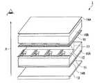
図1に示すように、本実施形態の液晶表示装置(表示装置)1は、TFTアレイ基板10Aと対向基板10Bとがシール材52によって貼り合わされ、このシール材52によって区画された領域内に液晶層11が封入されている。シール材52の形成領域の内側領域には、遮光性材料からなる遮光膜(周辺見切り)53が形成されている。シール材52の外側の周辺回路領域には、データ線駆動回路201および外部回路実装端子202がTFTアレイ基板10Aの一辺に沿って形成されており、この一辺に隣接する2辺に沿って走査線駆動回路104が形成されている。TFTアレイ基板10Aの残る一辺には、表示領域の両側に設けられた走査線駆動回路104の間を接続するための複数の配線105が設けられている。また、対向基板10Bの角部においては、TFTアレイ基板10Aと対向基板20との間で電気的導通をとるための基板間導通材106が配設されている。 As shown in FIG. 1, the liquid crystal display device (display device) 1 of the present embodiment includes a TFT array substrate 10 </ b> A and a counter substrate 10 </ b> B bonded together by a sealing
また、図2に示すように、TFTアレイ基板10Aの内側には画素電極15が形成され、対向基板10Bの内側には共通電極16が形成されている。更に、対向基板10Bと共通電極16の間には、カラーフィルタ12が形成されている。
また、TFTアレイ基板10Aと対向基板10Bの外側には、バックライトユニット13と、上下偏光板14A、14Bとが形成されている。
なお、本実施形態において、「内側」とは、液晶層11が形成されている側を意味し、「外側」とは、液晶層11が配置されていない側を意味している。As shown in FIG. 2, a
Further, a
In the present embodiment, “inner side” means the side where the
ここで、各構成要素について説明する。
TFTアレイ基板10A及び対向基板10Bは、ガラス・プラスチック等の透明基板によって構成されている。
また、画素電極15及び共通電極16は、ITO(インジウムスズ酸化物)等の透明導電体によって形成されている。更に、画素電極15は、TFTアレイ基板10Aに設けられたTFT(Thin film Transistor)に接続されており、当該TFTのスイッチング駆動に応じて、共通電極16と画素電極15の間の液晶層11に電圧を付与するようになっている。
液晶層11は、共通電極16と画素電極15によって付与された電圧値に応じて配列が変化する液晶分子を有している。本実施形態においては、液晶モードとしてTFTアレイ基板10Aと対向基板10B間で90度ねじれているTNモードを採用している。
また、上下偏光板14A、14Bは、相互の透過軸が直交するように配置されている。
このような液晶層11及び上下偏光板14A、14Bにおいては、液晶層11に付与される電圧値に応じて液晶分子の配列が変化することで、液晶層11及び上下偏光板14A、14Bを透過する光量が変わるようになっている。従って、液晶層11は、本発明の透光量制御部として機能するものであり、バックライトユニット13側から入射する光の光量を制御して、観察者側に所定の透光量で透過させるものである。
バックライトユニット13は、本発明の照明部として機能するものであり、光源と導光板によって構成されている。このような構成においては、光源から発光した光を導光板内部に均一に広げて、符号Aに示す方向に光源光を出射するようになっている。光源は、蛍光管や白色LED等からなるものである。導光板は、アクリル等の樹脂からなるものである。
このような構成を有する液晶表示装置1は、バックライトユニット13の発光を符号Aに向けて出射し、対向基板10B側から取り出す透過型液晶表示装置である。従って、バックライトユニット13の光源光を利用して液晶表示を行うようになっている。Here, each component will be described.
The
The
The
Further, the upper and lower
In such a
The
The liquid crystal display device 1 having such a configuration is a transmissive liquid crystal display device that emits light emitted from the
次に、カラーフィルタ12の構成について説明する。
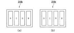
図3は、4つのドットによって1つの画素が構成されたカラーフィルタ12を示しており、RGBの3色ドットに加えて、Cを備えた4色ドットからなる画素構成を示している。また、カラーフィルタ12の平面配置図は、図3(a)に示すように左からR/G/B/Cの各色ドットを備えた構成となっている。なお、本実施形態においては、図3(b)に示すような配置、即ち、左からB/G/R/Cの各色ドットを備えた構成を採用してもよい。このようなドット構成を有するカラーフィルタ12は、図1に示す液晶表示装置1の表示領域の全面に配置されているものとする。Next, the configuration of the
FIG. 3 shows a
また、R/G/B/Cの各ドットは、バックライトユニット13の白色光が照射されることによって、当該白色光に含まれる所定の波長域、換言すれば所定色、の光を観察者側に透過させるものである。従って、R/G/B/Cの各ドットは、カラーフィルタ12を構成する各着色層であって、本発明の波長選択素子として機能するものである。 Further, each dot of R / G / B / C is irradiated with white light from the
図4は、カラーフィルタ12の波長選択特性を示しており、B、C、G、Rのピーク波長は、各々450nm、510nm、550nm、620nm以上を示している。
そして、本実施形態においては、B又はGのうち、Cのピーク波長(第4のピーク波長)に近いピーク波長(第2のピーク波長)を有しているドット(第2のドット)をCのドット(第4のドット)に隣接させないドット配列を採用している。
更に、B又はGのうち、Cのピーク波長に遠いピーク波長(第1のピーク波長)を有しているドットや、更に遠いピーク波長(第3のピーク波長)を有しているドット(第3のドット)をCのドットに隣接させたドット配列を採用している。FIG. 4 shows the wavelength selection characteristics of the
In this embodiment, among B or G, a dot (second dot) having a peak wavelength (second peak wavelength) close to the peak wavelength of C (fourth peak wavelength) is defined as C. A dot arrangement that is not adjacent to the other dot (fourth dot) is employed.
Furthermore, among B or G, a dot having a peak wavelength (first peak wavelength) far from the peak wavelength of C, or a dot having a peak wavelength (third peak wavelength) farther away (first peak wavelength) A dot arrangement in which 3 dots) are adjacent to C dots is employed.
具体的には、図4の波長選択特性を参照するように、B、Cのピーク波長の差が60nm(510nm−450nm)であり、G、Cのピーク波長の差が40nm(550nm−510nm)であるため、Cのピーク波長(第4のピーク波長)がGのピーク波長(第2のピーク波長)に近くなっている。また、Cのピーク波長がBのピーク波長(第1のピーク波長)に遠くなっている。
従って、Cのドット(第4のドット)に対して、Gのドット(第2のドット)を隣接させず、Bのドット(第1のドット)又はRのドット(第3のドット)を隣接させたドット配列を採用する。従って、図3(a)に示すように左からR/G/B/Cの順に配列された画素構造や、図3(b)に示すように左からB/G/R/Cの順に配列された画素構造が採用される。Specifically, as shown in the wavelength selection characteristics of FIG. 4, the difference between the peak wavelengths of B and C is 60 nm (510 nm-450 nm), and the difference between the peak wavelengths of G and C is 40 nm (550 nm-510 nm). Therefore, the C peak wavelength (fourth peak wavelength) is close to the G peak wavelength (second peak wavelength). Further, the peak wavelength of C is far from the peak wavelength of B (first peak wavelength).
Therefore, the G dot (second dot) is not adjacent to the C dot (fourth dot), but the B dot (first dot) or the R dot (third dot) is adjacent. Adopted dot arrangement. Therefore, the pixel structure arranged in the order of R / G / B / C from the left as shown in FIG. 3A, or the order of B / G / R / C from the left as shown in FIG. 3B. The pixel structure is adopted.
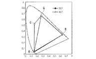
次に、図5を参照して、4色ドット(4CF)からなる画素構成を備えた液晶表示装置1と、RGBの3色ドット(3CF)からなる画素構成を備えた液晶表示装置を比較したxy色度特性を示して説明する。3色ドットの画素構成ではxy色度特性の三角形領域の色を実現することが可能となっているが、4色ドットの画素構成ではxy色度特性の四角形領域の色を実現することが可能となっている。従って、4色ドットの画素構成における本実施形態の液晶表示装置1が広色域を実現することが可能となっている。また、液晶表示装置1は、NTSC比115%を達成することが可能となる。 Next, referring to FIG. 5, the liquid crystal display device 1 having a pixel configuration composed of four color dots (4CF) and the liquid crystal display device having a pixel configuration composed of RGB three color dots (3CF) were compared. The xy chromaticity characteristics will be shown and described. With a three-color dot pixel configuration, it is possible to realize a triangular region color with xy chromaticity characteristics, but with a four-color dot pixel configuration, it is possible to realize a square region color with xy chromaticity characteristics. It has become. Therefore, the liquid crystal display device 1 of the present embodiment having a four-color dot pixel configuration can realize a wide color gamut. Further, the liquid crystal display device 1 can achieve an NTSC ratio of 115%.
上述したように、本実施形態においては、波長選択特性においてピーク波長が互いに近いGのドットとCのドットを隣接させずに、Bのドット又はRのドットにCのドットを隣接させた構成を有しているので、見かけ上の解像度低下やスジ状のラインを防止でき、画像品質を向上でき、広色域の画像表示が可能となる液晶表示装置を実現することができる。
ここで、CとGを隣接させた構成と比較して説明する。図4に示したように、CとGは非常に近い色相を有しているため、当該2つのドットを隣接させると液晶表示装置の見かけ上の解像度が低下し、ストライプ配列の画素構成においてスジ状のラインが見えることがある。このように解像度や画像品質が低下するのは、人間の視感度を考慮せずに、4色のドットを配置したことに起因している。
これに対し、本実施形態の液晶表示装置1は、互いにピーク波長が近いドット、即ち、概ね同色を示すCとGのドットを離間し、その間に他のドット(R、B)を配置しているので、人間の視感度として解像度や画像品質が向上した画像を表示することができる。従って、このような見かけ上の解像度低下やスジ状のラインを防止でき、画像品質を向上でき、広色域の画像表示が可能となる液晶表示装置を実現することができる。
また、上記のようにRGBのドットに加えてCのドットを具備すると共に、Cの配列を上記のように規定しているので、非常に広い色再現範囲を実現し、より自然光に近い広範囲の波長域の表示色で画像を表示することができるだけでなく、当該画像の解像度や画像品質を向上させて表示することができる。As described above, the present embodiment has a configuration in which a C dot is adjacent to a B dot or an R dot without adjoining a G dot and a C dot having peak wavelengths close to each other in wavelength selection characteristics. Therefore, it is possible to realize a liquid crystal display device that can prevent apparent resolution reduction and streak-like lines, improve image quality, and display an image with a wide color gamut.
Here, a description will be given in comparison with a configuration in which C and G are adjacent to each other. As shown in FIG. 4, since C and G have very close hues, when the two dots are adjacent to each other, the apparent resolution of the liquid crystal display device is lowered, and the stripe arrangement pixel configuration has a streak. Line may be visible. The decrease in resolution and image quality is caused by the arrangement of four color dots without considering human visibility.
On the other hand, in the liquid crystal display device 1 of the present embodiment, dots having peak wavelengths close to each other, that is, C and G dots having substantially the same color are separated from each other, and other dots (R, B) are arranged therebetween. Therefore, it is possible to display an image with improved resolution and image quality as human visibility. Therefore, it is possible to realize a liquid crystal display device that can prevent such apparent resolution reduction and streak-like lines, improve image quality, and display an image with a wide color gamut.
Further, as described above, in addition to RGB dots, C dots are provided, and the C arrangement is defined as described above, so that a very wide color reproduction range is realized, and a wide range closer to natural light is achieved. Not only can the image be displayed with the display color in the wavelength range, but also the resolution and image quality of the image can be improved and displayed.
また、xy色度特性において、BとGの座標を結ぶ線分よりも左側もしくは左上側の領域は、GとRの座標を結ぶ線分よりも右上側の領域や、RとBの座標を結ぶ線分よりも右下側の領域よりも、その領域が大きいために、より自然光に近い色を表現するための余地が大きい領域である。そこで、BとGの座標を結ぶ線分よりも左側もしくは左上側の領域に位置する色座標ドット、即ち、Cのドットを単位画素内に備えることで、上記、余地が大きい領域における色再現範囲を大きくすることができる。従って、自然光に近い広範囲の波長域の表示色を実現できる。
更に、Cを含む4色ドットを単位画素内に備える液晶表示装置1は、Yのドット等、他の色ドットを単位画素内に備える液晶表示装置と比較して、xy色度特性における表示可能領域を広範囲にすることができる。In the xy chromaticity characteristics, the region on the left side or the upper left side of the line segment connecting the coordinates of B and G represents the region on the upper right side of the line segment connecting the coordinates of G and R, or the coordinates of R and B. Since the area is larger than the area on the lower right side of the connecting line segment, this area has a large room for expressing a color closer to natural light. Therefore, by providing color coordinate dots located in the left or upper left area of the line connecting the coordinates of B and G, that is, C dots in the unit pixel, the color reproduction range in the above-described area having a large room. Can be increased. Therefore, display colors in a wide wavelength range close to natural light can be realized.
Furthermore, the liquid crystal display device 1 including four color dots including C in a unit pixel can display in xy chromaticity characteristics as compared with a liquid crystal display device including other color dots such as Y dots in the unit pixel. The area can be extensive.
また、液晶表示装置1は、RGBCの各ドットと、当該各ドットを透過する光量を制御する液晶層11とを備えている。これにより、RGBCの各ドットは、RGBCの各色の波長選択特性で光を透過させ、また、液晶層11が当該光の透光量を制御するので、非常に広い色再現範囲を実現し、より自然光に近い広範囲の波長域の表示色を透過光で表示することができる。更に、RGBCの各ドットが上記のように好適に規定配置されているので、解像度や画像品質を向上させて表示することができる。 The liquid crystal display device 1 also includes RGBC dots and a
また、液晶表示装置1は、RGBCの各ドットに対して、白色光を照射するバックライトユニット13を備えている。これにより、当該バックライトユニット13が、白色光でRGBCの各ドットを照射し、当該RGBCの各ドットがRGBCの各色の波長選択特性で光を透過させ、液晶層11が当該光の透光量を制御するので、非常に広い色再現範囲を実現し、より自然光に近い広範囲の波長域の表示色を透過光で表示することができる。更に、RGBCの各ドットが上記のように好適に規定配置されているので、解像度や画像品質を向上させて表示することができる。 In addition, the liquid crystal display device 1 includes a
なお、本実施形態においては、CとGを隣接させずに、R又はBにCを隣接させたドット配列を採用しているが、これを限定するものではない。例えば、波長選択特性において、Cのピーク波長(第4のピーク波長)がGのピーク波長(第1のピーク波長)よりもBのピーク波長(第2のピーク波長)に近い場合には、Cのドット(第4のドット)とBのドット(第2のドット)を隣接させずに、Gのドット(第1のドット)又はRのドット(第3のドット)をCのドットに隣接させる構成を採用してもよい。このようにすれば、ピーク波長が近いBとCを示す表示素子が隣接することにより生じる解像度の低下を防止できる。また、ストライプ配置の画素構成において、BとCを示す表示素子が隣接することにより生じるスジを抑制し、画像品質を向上できる。 In the present embodiment, a dot array in which C is adjacent to R or B without using C and G adjacent to each other is employed, but this is not a limitation. For example, in the wavelength selection characteristic, when the C peak wavelength (fourth peak wavelength) is closer to the B peak wavelength (second peak wavelength) than the G peak wavelength (first peak wavelength), C The G dot (first dot) or the R dot (third dot) is made adjacent to the C dot without making the next dot (fourth dot) and the B dot (second dot) adjacent to each other. A configuration may be adopted. In this way, it is possible to prevent a decrease in resolution caused by the adjacent display elements indicating B and C having close peak wavelengths. Further, in the pixel configuration in the stripe arrangement, streaks caused by adjacent display elements indicating B and C can be suppressed, and the image quality can be improved.
(第1実施形態の変形例)
次に、第1実施形態の変形例について説明する。
なお、第1実施形態と同一構成には同一符号を付して説明を簡略化する。
先に記載した第1実施形態においては、透過型の液晶表示装置について述べたが、本変形例においては、反射型の液晶表示装置に、上記のように規定されたドット配列を有するカラーフィルタ12を採用した場合について説明する。
この場合、液晶表示装置1は、外光を反射させて、当該反射光をRGBCの各ドットに照射する反射部を備えた構成を有している。反射部の具体例を説明すると、バックライトユニット13の代わりに、金属板や金属反射膜が成膜された基板等を設けた構成が採用される。(Modification of the first embodiment)
Next, a modification of the first embodiment will be described.
In addition, the same code | symbol is attached | subjected to the same structure as 1st Embodiment, and description is simplified.
In the first embodiment described above, the transmissive liquid crystal display device has been described. However, in the present modification, the reflective liquid crystal display device includes the
In this case, the liquid crystal display device 1 has a configuration including a reflection unit that reflects external light and irradiates the RGBC dots with the reflected light. A specific example of the reflecting portion will be described. A configuration in which a metal plate or a substrate on which a metal reflecting film is formed is provided instead of the
このような反射型の液晶表示装置においては、反射部が外光を反射させて、当該反射光をRGBCの各ドットに照射し、RGBCの各色の波長選択特性で反射光が透過する。更に、液晶層11が当該反射光の透光量を制御する。
上述したように、本変形例においては、非常に広い色再現範囲を実現し、より自然光に近い広範囲の波長域の表示色を反射光で表示することができる。更に、RGBCの各ドットが上記のように好適に規定配置されているので、解像度や画像品質を向上させて表示することができる。In such a reflective liquid crystal display device, the reflection part reflects external light, irradiates each of the RGBC dots with the reflected light, and the reflected light is transmitted with the wavelength selection characteristics of each color of RGBC. Further, the
As described above, in this modification, a very wide color reproduction range can be realized, and display colors in a wide wavelength range closer to natural light can be displayed with reflected light. Further, since the RGBC dots are suitably defined and arranged as described above, it is possible to display with improved resolution and image quality.
なお、上記においては、反射型の液晶表示装置について説明したが、反射部を備えた半透過反射型の液晶表示装置においても適用可能である。当該半透過反射型の液晶表示装置においては、バックライトユニット13を備えると共に、当該バックライトユニット13の外部に上記反射部を設けた構成が採用される。
また、半透過反射型の液晶表示装置の別形態として、RGBCの各ドットに透過表示領域と反射表示領域を有するマルチギャップ構造を採用することもできる。このようなマルチギャップ構造においては、反射表示領域のみに樹脂散乱膜や金属反射膜からなる反射部を設けた構成が採用される。また、透過表示領域においては、バックライトユニット13の照明光を利用した表示がなされる。In the above description, the reflective liquid crystal display device has been described. However, the present invention can also be applied to a transflective liquid crystal display device including a reflective portion. The transflective liquid crystal display device employs a configuration in which the
As another form of the transflective liquid crystal display device, a multi-gap structure having a transmissive display area and a reflective display area for each dot of RGBC can be adopted. In such a multi-gap structure, a configuration in which a reflection portion made of a resin scattering film or a metal reflection film is provided only in the reflective display region is employed. In the transmissive display area, display using illumination light of the
このような半透過反射型の液晶表示装置においては、反射部が外光を反射する場合と、バックライトユニット13が照明する場合とによって、RGBCの各ドットを照射し、RGBCの各色の波長選択特性で反射光や照明光が透過する。更に、液晶層11が当該光の透光量を制御する。
上述したように、本変形例においては、非常に広い色再現範囲を実現し、より自然光に近い広範囲の波長域の表示色を反射光で表示することができる。更に、RGBCの各ドットが上記のように好適に規定配置されているので、解像度や画像品質を向上させて表示することができる。In such a transflective liquid crystal display device, each wavelength of RGBC is selected by irradiating each dot of RGBC depending on whether the reflection part reflects external light or the
As described above, in this modification, a very wide color reproduction range can be realized, and display colors in a wide wavelength range closer to natural light can be displayed with reflected light. Further, since the RGBC dots are suitably defined and arranged as described above, it is possible to display with improved resolution and image quality.
(第1実施形態の別の変形例)
次に、第1実施形態の別の変形例について説明する。
なお、第1実施形態と同一構成には同一符号を付して説明を簡略化する。
先の第1実施形態においては、RGBの3色にCを加えた4色ドット配列を有するカラーフィルタ12について説明したが、以下では、Cに代えてYを採用した場合について説明する。(Another modification of the first embodiment)
Next, another modification of the first embodiment will be described.
In addition, the same code | symbol is attached | subjected to the same structure as 1st Embodiment, and description is simplified.
In the first embodiment described above, the
即ち、カラーフィルタ12は、RGBの3色ドットの他に、Yのドット(第4のドット、波長選択素子)を単位画素内に備えている。
ここで、波長選択特性において、Yのピーク波長(第4のピーク波長)が、Gのピーク波長(第1のピーク波長)よりもRのピーク波長(第2のピーク波長)に近い場合には、4色ドットの配列は、Yのドット(第4のドット)とRのドット(第2のドット)を隣接させずに、YのドットをGのドット(第1のドット)又はBのドット(第3のドット)に隣接させた構造が採用される。即ち、G/R/B/Y又は、B/R/G/Yの順に配列された画素構造が採用される。
また、波長選択特性において、Yのピーク波長(第4のピーク波長)が、Rのピーク波長(第1のピーク波長)よりもGのピーク波長(第2のピーク波長)に近い場合には、4色ドットの配列は、Yのドット(第4のドット)とGのドット(第2のドット)を隣接させずに、YのドットをRのドット(第1のドット)又はBのドット(第3のドット)に隣接させた構造が採用される。即ち、R/G/B/Y又は、B/G/R/Yの順に配列された画素構造が採用される。That is, the
Here, in the wavelength selection characteristics, when the Y peak wavelength (fourth peak wavelength) is closer to the R peak wavelength (second peak wavelength) than the G peak wavelength (first peak wavelength), The four-color dot arrangement is such that the Y dot (fourth dot) and the R dot (second dot) are not adjacent to each other, and the Y dot is replaced with the G dot (first dot) or B dot. A structure adjacent to (third dot) is employed. That is, a pixel structure arranged in the order of G / R / B / Y or B / R / G / Y is employed.
In the wavelength selection characteristic, when the peak wavelength of Y (fourth peak wavelength) is closer to the peak wavelength of G (second peak wavelength) than the peak wavelength of R (first peak wavelength), The four-color dot arrangement is such that the Y dot (fourth dot) and the G dot (second dot) are not adjacent to each other, and the Y dot is changed to the R dot (first dot) or the B dot ( A structure adjacent to the third dot) is employed. That is, a pixel structure arranged in the order of R / G / B / Y or B / G / R / Y is employed.
このようにすれば、カラーフィルタ12にバックライトユニット13の照明光が照射されると、Yを示すドットとピーク波長が近いドットが、互いに隣接することにより生じる解像度の低下を防止できる。また、ストライプ配置の画素構成において、従来問題となっていたスジを抑制し、画像品質を向上できる。更に、RGBYの4色を示すドットを備え、Yを示すドットに隣接する他のドットが上記のように好適に配置されているので、非常に広い色再現範囲を実現し、より自然光に近い広範囲の波長域の表示色で画像を表示することができるだけでなく、当該画像の解像度や画像品質を向上させて表示することができる。 In this way, when the illumination light of the
(第2実施形態)
以下、図6〜図10を参照し、本発明の第2実施形態について説明する。
本実施形態では、TFTをスイッチング素子として用いたアクティブマトリクス方式の有機EL装置の例を挙げて説明する。特にRGBCの4種類の高分子有機発光層を備えたカラー有機EL表示装置である。(Second Embodiment)
Hereinafter, a second embodiment of the present invention will be described with reference to FIGS.
In the present embodiment, an example of an active matrix organic EL device using TFTs as switching elements will be described. In particular, it is a color organic EL display device provided with four types of polymer organic light emitting layers of RGBC.
図6は本実施形態の有機EL装置の平面構造を示す図であり、図7は有機EL装置の画素構造を示す断面拡大図であり、図8は有機EL装置における有機EL層の平面配置図であり、図9は有機EL装置の発光波長特性を示す図であり、図10は有機EL装置の発光光のxy色度特性を説明するための図である。 FIG. 6 is a diagram showing a planar structure of the organic EL device of the present embodiment, FIG. 7 is an enlarged cross-sectional view showing a pixel structure of the organic EL device, and FIG. 8 is a plan layout diagram of an organic EL layer in the organic EL device. FIG. 9 is a diagram showing the emission wavelength characteristics of the organic EL device, and FIG. 10 is a diagram for explaining the xy chromaticity characteristics of the emitted light of the organic EL device.
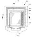
図6に示すように、本実施形態の有機EL装置(表示装置)200は、電気絶縁性を備える基板210と、スイッチング用TFT(後述)に接続された画素電極が基板210上にマトリックス状に配置されてなる画素電極域と、少なくとも画素電極域上に位置する平面視ほぼ矩形の画素部203(図中一点鎖線枠内)とを具備して構成されている。また、画素部203は、中央部分の実表示領域204(図中二点鎖線枠内)と、実表示領域204の周囲に配置されたダミー領域205(一点鎖線および二点鎖線の間の領域)とに区画されている。 As shown in FIG. 6, the organic EL device (display device) 200 of this embodiment includes a
実表示領域204には、それぞれ画素電極を有する表示領域R、C、G、BがA−B方向及びC−D方向に離間して配置されている。また、実表示領域204の図中両側には、走査線駆動回路280が配置されている。該走査線駆動回路280は、ダミー領域205の下側に位置して設けられている。さらに、実表示領域204の図中上側には、検査回路290が配置されている。該検査回路290は、ダミー領域205の下側に位置して設けられている。検査回路290は、有機EL装置200の作動状況を検査するための回路であって、例えば、検査結果を外部に出力する不図示の検査情報出力手段を備え、製造途中や出荷時の表示装置の品質、欠陥の検査を行うことができるように構成されている。 In the
走査線駆動回路280及び検査回路290の駆動電圧は、所定の電源部から駆動電圧導通部を介して印加されている。また、これら走査線駆動回路280及び検査回路290への駆動制御信号及び駆動電圧は、この有機EL装置200の作動制御を司る所定のメインドライバなどから駆動制御信号導通部等を介して送信および印加されるようになっている。なお、この場合の駆動制御信号とは、走査線駆動回路280及び検査回路290が信号を出力する際の制御に関連するメインドライバなどからの指令信号である。 The driving voltages of the scanning
次に、図7を用いて有機EL装置200の画素構造について説明する。
図7は、上記有機EL装置200における表示領域の断面構造を拡大した図である。
この図7にはR/C/G/Bの各色に対応する4つの画素領域の断面構造が示されている。有機EL装置200は、基板210上に、TFTなどの回路等が形成された回路素子部214、画素電極211、機能層210が形成された発光素子部311、及び陰極212が順次積層されて構成されている。
この有機EL装置200では、機能層210から基板210側に発した光が、回路素子部214及び基板210を透過して基板210の下側(観測者側)に出射されるとともに、機能層210から基板210の反対側に発した光が陰極212により反射されて、回路素子部214及び基板210を透過して基板210の下側(観測者側)に出射されるようになっている。Next, the pixel structure of the
FIG. 7 is an enlarged view of the cross-sectional structure of the display region in the
FIG. 7 shows a cross-sectional structure of four pixel regions corresponding to each color of R / C / G / B. The
In the
回路素子部214には、基板210上にシリコン酸化膜からなる下地保護膜と、各画素電極211に接続された駆動用TFT223と、層間絶縁膜244a、244bが形成されている。
発光素子部311は、複数の画素電極211…上の各々に積層された機能層210と、機能層210同士の間に配されて各機能層210を区画するバンク部212とを主体として構成されている。機能層210上には陰極212が配置されている。In the circuit element portion 214, a base protective film made of a silicon oxide film, a driving
The light emitting
発光素子部311において、バンク部212は基板210側に位置する無機物バンク層212aと基板210から離れて位置する有機物バンク層212bとが積層されて構成されている。
また、機能層210は、画素電極211上に積層された正孔注入/輸送層210aと、正孔注入/輸送層210a上に隣接して形成された有機EL層210bとから構成されている。
正孔注入/輸送層210aは、正孔を有機EL層210bに注入する機能を有するとともに、正孔を正孔注入/輸送層210a内部において輸送する機能を有する。このような正孔注入/輸送層210aを画素電極211と有機EL層210bの間に設けることにより、有機EL層210bの発光効率、寿命等の素子特性が向上する。また、有機EL層210bでは、正孔注入/輸送層210aから注入された正孔と、陰極212から注入される電子が有機EL層で再結合し、発光が得られる。In the light emitting
The
The hole injection /
陰極212は、発光素子部311の全面に形成されており、画素電極211と対になって機能層210に電流を流す役割を果たす。この陰極212は、本例ではフッ化リチウム層212a、カルシウム層212b、及びアルミニウム層212cが順次積層されて構成されている。 The
有機EL層210bは、赤色(R)に発光する赤色有機EL層210b1、シアン色(C)に発光するシアン色有機EL層210b2、緑色(G)に発光する緑色有機EL層210b3、及び青色(B)に発光する青色有機EL層210b4、の発光波長帯域が互いに異なる4種類からなり、各有機EL層210b1〜210b4が所定の配列(例えばストライプ状)で配置されている。
また、有機EL層210b1〜210b4は、溶媒と有機EL用高分子材料を混合して作製した組成物インクを、インクジェット法によって塗布することにより形成されたものである。また、このような有機EL層210b1〜210b4は、本発明の発光素子として機能するものである。The
The organic EL layers 210b1 to 210b4 are formed by applying a composition ink prepared by mixing a solvent and a polymer material for organic EL by an inkjet method. Further, such organic EL layers 210b1 to 210b4 function as the light emitting element of the present invention.
従って、有機EL層210bの平面配置図は、図8(a)に示すように左からR/C/G/Bの各色ドットを備えた構成となっている。なお、本実施形態においては、図3(b)に示すような配置、即ち、左からB/G/R/Cの各色ドットを備えた構成を採用してもよい。また、このようなドット構成を有する有機EL層210bは、図6に示す有機EL装置200の実表示領域204の全面に配置されているものとする。 Therefore, the plan view of the
図9は、有機EL装置の発光波長特性を示しており、B、C、G、Rのピーク波長は、各々470nm、500nm、550nm、640nm以上を示している。
そして、本実施形態においては、B又はGのうち、Cのピーク波長(第4のピーク波長)に近いピーク波長(第2のピーク波長)を有しているドット(第2のドット)をCのドット(第4のドット)に隣接させないドット配列を採用している。
更に、B又はGのうち、Cのピーク波長に遠いピーク波長(第1のピーク波長)を有しているドットや、更に遠いピーク波長(第3のピーク波長)を有しているドット(第3のドット)をCのドットに隣接させたドット配列を採用している。FIG. 9 shows the emission wavelength characteristics of the organic EL device, and the peak wavelengths of B, C, G, and R are 470 nm, 500 nm, 550 nm, and 640 nm or more, respectively.
In this embodiment, among B or G, a dot (second dot) having a peak wavelength (second peak wavelength) close to the peak wavelength of C (fourth peak wavelength) is defined as C. A dot arrangement that is not adjacent to the other dot (fourth dot) is employed.
Furthermore, among B or G, a dot having a peak wavelength (first peak wavelength) far from the peak wavelength of C, or a dot having a peak wavelength (third peak wavelength) farther away (first peak wavelength) A dot arrangement in which 3 dots) are adjacent to C dots is employed.
具体的には、図9の波長選択特性を参照するように、B、Cのピーク波長の差が30nm(500nm−470nm)であり、G、Cのピーク波長の差が50nm(550nm−500nm)であるため、Cのピーク波長(第4のピーク波長)がBのピーク波長(第2のピーク波長)に近くなっている。また、Cのピーク波長がGのピーク波長(第1のピーク波長)に遠くなっている。
従って、Cのドット(第4のドット)に対して、Bのドット(第2のドット)を隣接させず、Gのドット(第1のドット)又はRのドット(第3のドット)を隣接させたドット配列を採用する。従って、図7又は図8(a)に示すように左からR/C/G/Bの順に配列された画素構造や、図8(b)に示すように左からG/C/R/Bの順に配列された画素構造が採用される。Specifically, as shown in the wavelength selection characteristics of FIG. 9, the difference between the peak wavelengths of B and C is 30 nm (500 nm to 470 nm), and the difference between the peak wavelengths of G and C is 50 nm (550 nm to 500 nm). Therefore, the peak wavelength of C (fourth peak wavelength) is close to the peak wavelength of B (second peak wavelength). Further, the peak wavelength of C is far from the peak wavelength of G (first peak wavelength).
Therefore, the B dot (second dot) is not adjacent to the C dot (fourth dot), but the G dot (first dot) or the R dot (third dot) is adjacent. Adopted dot arrangement. Accordingly, as shown in FIG. 7 or FIG. 8 (a), the pixel structure is arranged in the order of R / C / G / B from the left, or G / C / R / B from the left as shown in FIG. 8 (b). A pixel structure arranged in this order is employed.
次に、図10を参照して、4色ドットの画素構成を備えた有機EL装置200(4色発光タイプ)と、RGBの3色ドットの画素構成を備えた有機EL装置(3色発光タイプ)の発光特性を比較したxy色度特性について説明する。3色ドットの画素構成ではxy色度特性の三角形領域の色を実現することが可能となっているが、4色ドットの画素構成ではxy色度特性の四角形領域の色を実現することが可能となっている。従って、4色ドットの画素構成における本実施形態の有機EL装置200が広色域を実現することが可能となっている。また、有機EL装置200は、NTSC比120%を達成することが可能となる。 Next, referring to FIG. 10, an organic EL device 200 (four-color emission type) having a pixel configuration of four-color dots and an organic EL device (three-color emission type) having a pixel configuration of RGB three-color dots. The xy chromaticity characteristics comparing the light emission characteristics of) will be described. With a three-color dot pixel configuration, it is possible to realize a triangular region color with xy chromaticity characteristics, but with a four-color dot pixel configuration, it is possible to realize a square region color with xy chromaticity characteristics. It has become. Therefore, the
上述したように、本実施形態においては、発光波長特性においてピーク波長が互いに近いBのドットとCのドットを隣接させずに、Gのドット又はRのドットにCのドットを隣接させた構成を有しているので、見かけ上の解像度低下やスジ状のラインを防止でき、画像品質を向上でき、広色域の画像表示が可能となる有機EL装置を実現することができる。
ここで、CとBを隣接させた構成と比較して説明する。図9に示したように、CとBは非常に近い色相を有しているため、当該2つのドットを隣接させると有機EL装置の見かけ上の解像度が低下し、ストライプ配列の画素構成においてスジ状のラインが見えることがある。このように解像度や画像品質が低下するのは、人間の視感度を考慮せずに、4色のドットを配置したことに起因している。
これに対し、本実施形態の有機EL装置200は、互いにピーク波長が近いドット、即ち、概ね同色を示すCとBのドットを離間し、その間に他のドット(R、G)を配置しているので、人間の視感度として解像度や画像品質が向上した画像を表示することができる。従って、このような見かけ上の解像度低下やスジ状のラインを防止でき、画像品質を向上でき、広色域の画像表示が可能となる液晶表示装置を実現することができる。
また、上記のようにRGBのドットに加えてCのドットを具備すると共に、Cの配列を上記のように規定しているので、非常に広い色再現範囲を実現し、より自然光に近い広範囲の波長域の表示色で画像を表示することができるだけでなく、当該画像の解像度や画像品質を向上させて表示することができる。As described above, the present embodiment has a configuration in which the C dot is adjacent to the G dot or the R dot without adjoining the B dot and the C dot whose peak wavelengths are close to each other in the emission wavelength characteristics. Therefore, it is possible to realize an organic EL device that can prevent apparent resolution reduction and streak-like lines, improve image quality, and display an image with a wide color gamut.
Here, a description will be given in comparison with a configuration in which C and B are adjacent to each other. As shown in FIG. 9, since C and B have very close hues, when the two dots are adjacent to each other, the apparent resolution of the organic EL device is lowered, and the stripe arrangement pixel structure has a streak. Line may be visible. The decrease in resolution and image quality is caused by the arrangement of four color dots without considering human visibility.
On the other hand, the
Further, as described above, in addition to RGB dots, C dots are provided, and the C arrangement is defined as described above, so that a very wide color reproduction range is realized, and a wide range closer to natural light is achieved. Not only can the image be displayed with the display color in the wavelength range, but also the resolution and image quality of the image can be improved and displayed.
また、xy色度特性において、BとGの座標を結ぶ線分よりも左側もしくは左上側の領域は、GとRの座標を結ぶ線分よりも右上側の領域や、RとBの座標を結ぶ線分よりも右下側の領域よりも、その領域が大きいために、より自然光に近い色を表現するための余地が大きい領域である。そこで、BとGの座標を結ぶ線分よりも左側もしくは左上側の領域に位置する色座標ドット、即ち、Cのドットを単位画素内に備えることで、上記、余地が大きい領域における色再現範囲を大きくすることができる。従って、自然光に近い広範囲の波長域の表示色を実現できる。
更に、Cを含む4色ドットを単位画素内に備える有機EL装置200は、Yのドット等、他の色ドットを単位画素内に備える有機EL装置と比較して、xy色度特性における表示可能領域を広範囲にすることができる。In the xy chromaticity characteristics, the region on the left side or the upper left side of the line segment connecting the coordinates of B and G represents the region on the upper right side of the line segment connecting the coordinates of G and R, or the coordinates of R and B. Since the area is larger than the area on the lower right side of the connecting line segment, this area has a large room for expressing a color closer to natural light. Therefore, by providing color coordinate dots located in the left or upper left area of the line connecting the coordinates of B and G, that is, C dots in the unit pixel, the color reproduction range in the above-described area having a large room. Can be increased. Therefore, display colors in a wide wavelength range close to natural light can be realized.
Furthermore, the
なお、本実施形態においては、CとBを隣接させずに、R又はGにCを隣接させたドット配列を採用しているが、これを限定するものではない。例えば、発光波長特性において、Cのピーク波長(第4のピーク波長)がBのピーク波長(第1のピーク波長)よりもGのピーク波長(第2のピーク波長)に近い場合には、Cのドット(第4のドット)とGのドット(第2のドット)を隣接させずに、Bのドット(第1のドット)又はRのドット(第3のドット)をCに隣接させる構成を採用してもよい。このようにすれば、ピーク波長が近いGとCを示す表示素子が隣接することにより生じる解像度の低下を防止できる。また、ストライプ配置の画素構成において、BとCを示す表示素子が隣接することにより生じるスジを抑制し、画像品質を向上できる。 In the present embodiment, a dot arrangement in which C is adjacent to R or G without using C and B adjacent to each other is employed, but this is not a limitation. For example, in the emission wavelength characteristic, when the C peak wavelength (fourth peak wavelength) is closer to the G peak wavelength (second peak wavelength) than the B peak wavelength (first peak wavelength), C A configuration in which the B dot (first dot) or the R dot (third dot) is adjacent to C without adjoining the dot (fourth dot) and the G dot (second dot). It may be adopted. In this way, it is possible to prevent a decrease in resolution caused by the adjacent display elements indicating G and C having close peak wavelengths. Further, in the pixel configuration in the stripe arrangement, streaks caused by adjacent display elements indicating B and C can be suppressed, and the image quality can be improved.
また、本実施形態においては、RGBの3色にCを加えた4色ドットの画素構成を採用しているが、上記第1実施形態の別の変形例に示したようにCに代えてYを採用してもよい。この場合においても、発光波長特性において、Yのピーク波長に近いピーク波長を有するドットと当該Yのドットを隣接させずに、Yのピーク波長に遠いピーク波長を有するドットと当該Yのドットを隣接させて配置することで、先に記載した同様の効果が得られる。 In the present embodiment, a pixel configuration of four-color dots in which C is added to the three colors of RGB is adopted, but instead of C as shown in another modification of the first embodiment, Y May be adopted. Even in this case, in the emission wavelength characteristic, the dot having the peak wavelength close to the Y peak wavelength and the Y dot are not adjacent to each other, and the dot having the peak wavelength far from the Y peak wavelength and the Y dot are adjacent to each other. By arranging them, the same effect as described above can be obtained.
また、本実施形態では高分子有機発光層を備えた有機EL装置200について述べたが、低分子有機発光層を備えた有機EL装置200においても本発明が適用可能である。また、有機EL装置に限らず、LED表示装置や、プラズマディスプレイ、電界放出ディスプレイ、CRTディスプレイ、DMD(Digital Micro mirror Device)等、単位画素内に複数の着色ドットを備えた表示装置に本発明を適用することによって、同様の効果が得られる。 Further, in the present embodiment, the
なお、上記の第1及び第2実施形態においては、4色ドットを備えた表示装置(液晶表示装置1、有機EL装置200)について説明したが、当該4色ドットに更に別の波長領域のドットを加えた5色ドットや、6色ドットを構成してもよい。この場合には、RGBを含む4色ドットにおける配列を上記実施形態のように規定することで、上記同様の効果が得られる。 In the first and second embodiments described above, the display device (the liquid crystal display device 1 and the organic EL device 200) having four color dots has been described. A five-color dot or a six-color dot to which is added may be configured. In this case, the same effect as described above can be obtained by defining the arrangement of four color dots including RGB as in the above embodiment.
(電子機器)
図11(a)〜(c)は、本発明の電子機器の実施形態を示している。
本例の電子機器は、上述した液晶表示装置や有機EL装置を表示手段として備えている。
図11(a)は、携帯電話の一例を示した斜視図である。図11(a)において、符号1000は携帯電話本体を示し、符号1001は前記の表示装置を用いた表示部を示している。
図11(b)は、腕時計型電子機器の一例を示した斜視図である。図11(b)において、符号1100は時計本体を示し、符号1101は前記の表示装置を用いた表示部を示している。
図11(c)は、ワープロ、パソコンなどの携帯型情報処理装置の一例を示した斜視図である。図11(c)において、符号1200は情報処理装置、符号1202はキーボードなどの入力部、符号1204は情報処理装置本体、符号1206は前記の表示装置を用いた表示部を示している。
図11(a)〜(c)に示すそれぞれの電子機器は、表示部に本発明の表示装置を備えているので、非常に広い色再現範囲を実現し、より自然光に近い広範囲の波長域の表示色で画像を表示することができるだけでなく、当該画像の解像度や画像品質を向上させて表示することが可能な電子機器を実現できる。(Electronics)
11 (a) to 11 (c) show an embodiment of the electronic apparatus of the present invention.
The electronic apparatus of this example includes the above-described liquid crystal display device and organic EL device as display means.
FIG. 11A is a perspective view showing an example of a mobile phone. In FIG. 11A,
FIG. 11B is a perspective view showing an example of a wristwatch type electronic device. In FIG. 11B,
FIG. 11C is a perspective view showing an example of a portable information processing apparatus such as a word processor or a personal computer. In FIG. 11C,
Each of the electronic devices shown in FIGS. 11A to 11C includes the display device of the present invention in the display unit, and thus realizes a very wide color reproduction range and has a wide wavelength range closer to natural light. It is possible to realize an electronic apparatus that can display an image with a display color as well as an improved resolution and image quality of the image.
以上、添付図面を参照しながら本発明に係る好適な実施形態について説明したが、本発明は係る例に限定されないことは言うまでもない。上述した例において示した各構成部材の諸形状や組み合わせ等は一例であって、本発明の主旨から逸脱しない範囲において設計要求等に基づき種々変更可能である。 As described above, the preferred embodiments according to the present invention have been described with reference to the accompanying drawings, but the present invention is not limited to the examples. Various shapes, combinations, and the like of the constituent members shown in the above-described examples are examples, and various modifications can be made based on design requirements and the like without departing from the gist of the present invention.
1 液晶表示装置(表示装置)、11 液晶層(透光量制御部)、12 カラーフィルタ、13 バックライトユニット(照明部)、200 有機EL装置(表示装置)、210b 有機EL層(発光素子)、R、G、B 第1のドット(波長選択素子)、R、G、B 第2のドット(波長選択素子)、R、G、B 第3のドット(波長選択素子)、C シアン色(第4のドット、波長選択素子)、Y イエロー色(第4のドット、波長選択素子)
DESCRIPTION OF SYMBOLS 1 Liquid crystal display device (display device), 11 Liquid crystal layer (light transmission control part), 12 Color filter, 13 Backlight unit (illumination part), 200 Organic electroluminescent apparatus (display apparatus), 210b Organic electroluminescent layer (light emitting element) , R, G, B first dot (wavelength selection element), R, G, B second dot (wavelength selection element), R, G, B third dot (wavelength selection element), C cyan color ( 4th dot, wavelength selection element), Y yellow color (4th dot, wavelength selection element)
Claims (10)
Translated fromJapanese前記第1〜第4の波長選択素子は前記単位画素において列状に配列され、
複数の前記単位画素はストライプ状に配置され、
白色光が照射されたとき、前記第3の波長選択素子の透過光は赤色であり、
白色光に対する波長選択特性において、前記第1の波長選択素子は第1のピーク波長を有し、前記第2の波長選択素子は第2のピーク波長を有し、前記第4の波長選択素子は第4のピーク波長を有し、
前記第1のピーク波長と前記第2のピーク波長と前記第4のピーク波長はいずれも、前記第3の波長選択素子によって選択される波長よりも短く、
前記第4のピーク波長は、前記第1のピーク波長と前記第2のピーク波長の間に位置するとともに、前記第1のピーク波長よりも前記第2のピーク波長に近く、
前記第1〜第4の波長選択素子は、
前記第4の波長選択素子と前記第2の波長選択素子とは互いに隣り合わず、
前記第2の波長選択素子は、前記第1の波長選択素子と前記第3の波長選択素子のいずれとも互いに隣り合い、
前記第4の波長選択素子は、前記第1の波長選択素子と前記第3の波長選択素子のいずれともに互いに隣り合うように、配置されていることを特徴とする表示装置。A display devicecomprising a plurality of unit pixels composed of first to fourth wavelength selection elements, and a light transmission control unit for controlling the amount of light transmitted through the wavelength selection elements,
The first to fourth wavelength selection elements are arranged in a row in the unit pixel,
The plurality of unit pixels are arranged in a stripe shape,
When white light is irradiated, the transmitted light of the third wavelength selection element is red,
In the wavelength selection characteristic for white light, the first wavelength selection element has a first peak wavelength, the second wavelength selection element has a second peak wavelength, and the fourth wavelength selection element is Having a fourth peak wavelength;
The first peak wavelength, the second peak wavelength, and the fourth peak wavelength are all shorter than the wavelength selected by the third wavelength selection element,
The fourth peak wavelength is located between the first peak wavelength and the second peak wavelength, and is closer to the second peak wavelength than the first peak wavelength,
The first to fourth wavelength selection elements are:
The fourth wavelength selection elementand the second wavelength selection elementare not adjacent to each other ,
The second wavelength selection element is adjacent to both the first wavelength selection element and the third wavelength selection element,
The display device,wherein the fourth wavelength selection element is arrangedso that both the first wavelength selection element and the third wavelength selection element are adjacent to each other .
前記第1〜第4のドットは前記単位画素において列状に配列され、
前記第1〜第4のドットから出射される光の色は互いに異なり、
前記ドットから出射される光の波長特性において、前記第1のドットは第1のピーク波長を有し、前記第2のドットは第2のピーク波長を有し、前記第3のドットは第3のピーク波長を有し、前記第4のドットは第4のピーク波長を有し、
前記第4のピーク波長は、前記第1のピーク波長と前記第2のピーク波長の間に位置するとともに、前記第1のピーク波長よりも前記第2のピーク波長に近く、
前記第1〜第4のドットは、
前記第4のドットと前記第2のドットとは互いに隣り合わず、
前記第2のドットは、前記第1のドットと前記第3のドットのいずれとも互いに隣り合い、
前記第4のドットは、前記第1のドットと前記第3のドットのいずれともに互いに隣り合うように、配置されていることを特徴とする表示装置。A display device in which unit pixels composed of first to fourth dots having light emitting elements are arranged in a plurality of stripes,
The first to fourth dots are arranged in a row in the unit pixel,
The colors of light emitted from the first to fourth dots are different from each other,
In the wavelength characteristics of light emitted from the dots, the first dots have a first peak wavelength, the second dots have a second peak wavelength, and the third dots are third. And the fourth dot has a fourth peak wavelength,
The fourth peak wavelength is located between the first peak wavelength and the second peak wavelength, and is closer to the second peak wavelength than the first peak wavelength,
The first to fourth dots are
The fourth dotand the second dotare not adjacent to each other ,
The second dot is adjacent to both the first dot and the third dot;
The display device,wherein the fourth dot is arrangedso that both the first dot and the third dot are adjacent to each other .
前記第1〜第4の波長選択素子は前記単位画素において列状に配列され、
複数の単位画素は複数ストライプ状に配置され、
白色光が照射されたとき、前記第3の波長選択素子の透過光は赤色であり、
白色光に対する波長選択特性において、前記第1の波長選択素子は第1のピーク波長を有し、前記第2の波長選択素子は第2のピーク波長を有し、前記第4の波長選択素子は第4のピーク波長を有し、
前記第1のピーク波長と前記第2のピーク波長と前記第4のピーク波長はいずれも、前記第3の波長選択素子によって選択される波長よりも短く、
前記第4のピーク波長は、前記第1のピーク波長と前記第2のピーク波長の間に位置するとともに、前記第1のピーク波長よりも前記第2のピーク波長に近く、
前記第1〜第4の波長選択素子は、
前記第4の波長選択素子と前記第2の波長選択素子とは互いに隣り合わず、
前記第2の波長選択素子は、前記第1の波長選択素子と前記第3の波長選択素子のいずれとも互いに隣り合い、
前記第4の波長選択素子は、前記第1の波長選択素子と前記第3の波長選択素子のいずれともに互いに隣り合うように、配置されていることを特徴とする表示装置用カラーフィルタ。A color filterfor adisplay devicecomprising a plurality of unit pixels composed of first to fourth wavelength selection elements,
The first to fourth wavelength selection elements are arranged in a row in the unit pixel,
A plurality of unit pixels are arranged in a plurality of stripes,
When white light is irradiated, the transmitted light of the third wavelength selection element is red,
In the wavelength selection characteristic for white light, the first wavelength selection element has a first peak wavelength, the second wavelength selection element has a second peak wavelength, and the fourth wavelength selection element is Having a fourth peak wavelength;
The first peak wavelength, the second peak wavelength, and the fourth peak wavelength are all shorter than the wavelength selected by the third wavelength selection element,
The fourth peak wavelength is located between the first peak wavelength and the second peak wavelength, and is closer to the second peak wavelength than the first peak wavelength,
The first to fourth wavelength selection elements are:
The fourth wavelength selection elementand the second wavelength selection elementare not adjacent to each other ,
The second wavelength selection element is adjacent to both the first wavelength selection element and the third wavelength selection element,
The color filterfor adisplay device,wherein the fourth wavelength selection element is disposedso that both the first wavelength selection element and the third wavelength selection element are adjacent to each other .
Priority Applications (7)
| Application Number | Priority Date | Filing Date | Title |
|---|---|---|---|
| JP2004129655AJP4211669B2 (en) | 2004-04-26 | 2004-04-26 | Display device, color filter for display device, and electronic device |
| US11/061,441US7443469B2 (en) | 2004-04-26 | 2005-02-22 | Display device, color filter, and electronic apparatus |
| EP05006870AEP1591987B1 (en) | 2004-04-26 | 2005-03-30 | Display device, color filter, and electronic apparatus |
| TW094111694ATW200537184A (en) | 2004-04-26 | 2005-04-13 | Display device, color filter, and electronic equipment |
| KR1020050033019AKR100739395B1 (en) | 2004-04-26 | 2005-04-21 | Display device, color filter, and electronic apparatus |
| CN201210201532.2ACN102722051B (en) | 2004-04-26 | 2005-04-26 | Display device, color filter and electronic equipment |
| CN2005100678275ACN1700265B (en) | 2004-04-26 | 2005-04-26 | Display device, color filter and electronic equipment |
Applications Claiming Priority (1)
| Application Number | Priority Date | Filing Date | Title |
|---|---|---|---|
| JP2004129655AJP4211669B2 (en) | 2004-04-26 | 2004-04-26 | Display device, color filter for display device, and electronic device |
Publications (2)
| Publication Number | Publication Date |
|---|---|
| JP2005309305A JP2005309305A (en) | 2005-11-04 |
| JP4211669B2true JP4211669B2 (en) | 2009-01-21 |
Family
ID=34934576
Family Applications (1)
| Application Number | Title | Priority Date | Filing Date |
|---|---|---|---|
| JP2004129655AExpired - LifetimeJP4211669B2 (en) | 2004-04-26 | 2004-04-26 | Display device, color filter for display device, and electronic device |
Country Status (6)
| Country | Link |
|---|---|
| US (1) | US7443469B2 (en) |
| EP (1) | EP1591987B1 (en) |
| JP (1) | JP4211669B2 (en) |
| KR (1) | KR100739395B1 (en) |
| CN (2) | CN1700265B (en) |
| TW (1) | TW200537184A (en) |
Families Citing this family (21)
| Publication number | Priority date | Publication date | Assignee | Title |
|---|---|---|---|---|
| WO2006109567A1 (en) | 2005-04-05 | 2006-10-19 | Sharp Kabushiki Kaisha | Display device compatible with reflection and transmission |
| WO2006109577A1 (en)* | 2005-04-05 | 2006-10-19 | Sharp Kabushiki Kaisha | Color filter substrate and display |
| TWI381742B (en)* | 2005-10-13 | 2013-01-01 | Seiko Epson Corp | Image display device, electronic apparatus, and pixel location determining method |
| US7889216B2 (en)* | 2005-10-13 | 2011-02-15 | Seiko Epson Corporation | Image display device, electronic apparatus, and pixel location determining method |
| US20070103056A1 (en)* | 2005-11-08 | 2007-05-10 | Eastman Kodak Company | OLED device having improved light output |
| JP2007139948A (en)* | 2005-11-16 | 2007-06-07 | Epson Imaging Devices Corp | Electrooptical device and electronic equipment |
| KR101119180B1 (en)* | 2006-01-23 | 2012-03-20 | 삼성전자주식회사 | Apparatus of emitting light and liquid crystal display device having the same |
| JP2007251318A (en)* | 2006-03-14 | 2007-09-27 | Juichi Nakai | Color image display apparatus with the same expressive power as that of actual object |
| JP2007279097A (en)* | 2006-04-03 | 2007-10-25 | Epson Imaging Devices Corp | Liquid crystal device and electronic apparatus |
| JP4333768B2 (en)* | 2007-04-06 | 2009-09-16 | ソニー株式会社 | Display device |
| CN101970226B (en)* | 2008-03-14 | 2014-07-02 | 东丽株式会社 | Laminated film |
| JP5315761B2 (en)* | 2008-04-15 | 2013-10-16 | セイコーエプソン株式会社 | Organic electroluminescence device |
| TWI386688B (en)* | 2009-01-08 | 2013-02-21 | Au Optronics Corp | Display device and display panel and color filter thereof |
| WO2011030604A1 (en) | 2009-09-09 | 2011-03-17 | シャープ株式会社 | Color filter substrate, liquid crystal display panel and liquid crystal display device |
| JP5650918B2 (en)* | 2010-03-26 | 2015-01-07 | 株式会社ジャパンディスプレイ | Image display device |
| JP5699317B2 (en)* | 2010-09-08 | 2015-04-08 | 大日本印刷株式会社 | Color filter manufacturing method and liquid crystal display |
| JP6193096B2 (en)* | 2013-11-08 | 2017-09-06 | 昭和電工株式会社 | Liquid crystal display |
| JP2015128003A (en) | 2013-12-27 | 2015-07-09 | ソニー株式会社 | Display device and electronic apparatus |
| CN104777639A (en)* | 2015-05-06 | 2015-07-15 | 京东方科技集团股份有限公司 | Array substrate and driving method, display panel and display device thereof |
| JP2017146463A (en)* | 2016-02-17 | 2017-08-24 | 株式会社ジャパンディスプレイ | Display device |
| US20210143135A1 (en)* | 2019-11-12 | 2021-05-13 | Daktronics, Inc. | Enhanced color gamut for electronic displays |
Family Cites Families (17)
| Publication number | Priority date | Publication date | Assignee | Title |
|---|---|---|---|---|
| GB2122794B (en) | 1982-06-15 | 1985-09-18 | Standard Telephones Cables Ltd | Liquid crystal display |
| US4800375A (en) | 1986-10-24 | 1989-01-24 | Honeywell Inc. | Four color repetitive sequence matrix array for flat panel displays |
| JP2684426B2 (en) | 1989-09-06 | 1997-12-03 | 富士写真フイルム株式会社 | Color video system |
| JP2566087B2 (en)* | 1992-01-27 | 1996-12-25 | 株式会社東芝 | Colored microlens array and manufacturing method thereof |
| JPH08248410A (en) | 1995-03-15 | 1996-09-27 | Toshiba Corp | Color image display device |
| US6023315A (en)* | 1995-07-04 | 2000-02-08 | Sharp Kabushiki Kaisha | Spatial light modulator and directional display |
| TW417074B (en) | 1996-09-06 | 2001-01-01 | Matsushita Electric Industrial Co Ltd | Display device |
| JPH1184365A (en) | 1997-09-02 | 1999-03-26 | Seiko Epson Corp | Liquid crystal devices and electronic equipment |
| GB9818092D0 (en)* | 1998-08-19 | 1998-10-14 | Cambridge Display Tech Ltd | Display devices |
| US6853980B1 (en)* | 1999-09-07 | 2005-02-08 | Bitstream Inc. | System for selecting, distributing, and selling fonts |
| JP2001306023A (en) | 2000-04-18 | 2001-11-02 | Seiko Epson Corp | Image display device |
| US6570584B1 (en)* | 2000-05-15 | 2003-05-27 | Eastman Kodak Company | Broad color gamut display |
| IL159246A0 (en) | 2001-06-11 | 2004-06-01 | Genoa Technologies Ltd | Device, system and method for color display |
| JP2003161912A (en)* | 2001-09-13 | 2003-06-06 | Hit Design:Kk | Three-dimensional image display device and color reproduction method in three-dimensional image display |
| CN101840687B (en) | 2002-04-11 | 2013-09-18 | 格诺色彩技术有限公司 | Color display device with enhanced attributes and method thereof |
| US7518584B2 (en) | 2003-01-28 | 2009-04-14 | Koninklijke Philips Electronics N.V. | Method of displaying an image on a color display |
| JP2005062833A (en) | 2003-07-29 | 2005-03-10 | Seiko Epson Corp | Color filter, color image display device, and electronic apparatus |
- 2004
- 2004-04-26JPJP2004129655Apatent/JP4211669B2/ennot_activeExpired - Lifetime
- 2005
- 2005-02-22USUS11/061,441patent/US7443469B2/enactiveActive
- 2005-03-30EPEP05006870Apatent/EP1591987B1/ennot_activeExpired - Lifetime
- 2005-04-13TWTW094111694Apatent/TW200537184A/ennot_activeIP Right Cessation
- 2005-04-21KRKR1020050033019Apatent/KR100739395B1/ennot_activeExpired - Lifetime
- 2005-04-26CNCN2005100678275Apatent/CN1700265B/ennot_activeExpired - Lifetime
- 2005-04-26CNCN201210201532.2Apatent/CN102722051B/ennot_activeExpired - Lifetime
Also Published As
| Publication number | Publication date |
|---|---|
| CN102722051B (en) | 2016-03-09 |
| EP1591987A3 (en) | 2006-01-11 |
| US7443469B2 (en) | 2008-10-28 |
| KR20060047313A (en) | 2006-05-18 |
| CN1700265B (en) | 2012-07-18 |
| JP2005309305A (en) | 2005-11-04 |
| EP1591987A2 (en) | 2005-11-02 |
| KR100739395B1 (en) | 2007-07-13 |
| CN102722051A (en) | 2012-10-10 |
| TW200537184A (en) | 2005-11-16 |
| CN1700265A (en) | 2005-11-23 |
| EP1591987B1 (en) | 2012-01-11 |
| TWI312143B (en) | 2009-07-11 |
| US20050236950A1 (en) | 2005-10-27 |
Similar Documents
| Publication | Publication Date | Title |
|---|---|---|
| JP4211669B2 (en) | Display device, color filter for display device, and electronic device | |
| JP4003714B2 (en) | Electro-optical device and electronic apparatus | |
| JP5650918B2 (en) | Image display device | |
| JP4572854B2 (en) | Liquid crystal device and electronic device | |
| JP4145852B2 (en) | Electro-optical device, color filter, and electronic device | |
| CN101162320A (en) | Color display, liquid crystal display, and translucent liquid crystal display | |
| KR20110070816A (en) | Display device | |
| JP2008191287A (en) | Liquid crystal display device | |
| JP4082379B2 (en) | Liquid crystal display device and electronic device | |
| JP2007206392A (en) | Electro-optical device, driving method thereof, and electronic equipment | |
| JP4306779B2 (en) | Display device | |
| JP4581796B2 (en) | Display device and electronic device | |
| JP2007114295A (en) | Display device and electronic device | |
| JP2007094025A (en) | Electrooptic device and electronic equipment | |
| JP2007133059A (en) | Electro-optical device, method for manufacturing the same, and electronic apparatus | |
| JP4626478B2 (en) | Image display device, electronic device, and pixel arrangement design method | |
| JP2007226084A (en) | Display device, color filter, liquid crystal display device provided with them, panel for liquid crystal display device and electronic equipment | |
| JP2007086506A (en) | Electrooptical device and electronic equipment | |
| JP2007279094A (en) | Liquid crystal device and electronic equipment | |
| JP2007017928A (en) | Electro-optical apparatus and electronic equipment | |
| JP2007140240A (en) | Electrooptical device and electronic equipment | |
| JP2007240658A (en) | Image display device, electronic device, and pixel arrangement design method | |
| JP2010008844A (en) | Display device and electronic apparatus |
Legal Events
| Date | Code | Title | Description |
|---|---|---|---|
| A977 | Report on retrieval | Free format text:JAPANESE INTERMEDIATE CODE: A971007 Effective date:20070126 | |
| RD04 | Notification of resignation of power of attorney | Free format text:JAPANESE INTERMEDIATE CODE: A7424 Effective date:20070403 | |
| A131 | Notification of reasons for refusal | Free format text:JAPANESE INTERMEDIATE CODE: A131 Effective date:20080122 | |
| A521 | Request for written amendment filed | Free format text:JAPANESE INTERMEDIATE CODE: A523 Effective date:20080318 | |
| A131 | Notification of reasons for refusal | Free format text:JAPANESE INTERMEDIATE CODE: A131 Effective date:20080520 | |
| A521 | Request for written amendment filed | Free format text:JAPANESE INTERMEDIATE CODE: A523 Effective date:20080717 | |
| TRDD | Decision of grant or rejection written | ||
| A01 | Written decision to grant a patent or to grant a registration (utility model) | Free format text:JAPANESE INTERMEDIATE CODE: A01 Effective date:20081007 | |
| A01 | Written decision to grant a patent or to grant a registration (utility model) | Free format text:JAPANESE INTERMEDIATE CODE: A01 | |
| A61 | First payment of annual fees (during grant procedure) | Free format text:JAPANESE INTERMEDIATE CODE: A61 Effective date:20081020 | |
| FPAY | Renewal fee payment (event date is renewal date of database) | Free format text:PAYMENT UNTIL: 20111107 Year of fee payment:3 | |
| R150 | Certificate of patent or registration of utility model | Ref document number:4211669 Country of ref document:JP Free format text:JAPANESE INTERMEDIATE CODE: R150 Free format text:JAPANESE INTERMEDIATE CODE: R150 | |
| FPAY | Renewal fee payment (event date is renewal date of database) | Free format text:PAYMENT UNTIL: 20111107 Year of fee payment:3 | |
| FPAY | Renewal fee payment (event date is renewal date of database) | Free format text:PAYMENT UNTIL: 20121107 Year of fee payment:4 | |
| FPAY | Renewal fee payment (event date is renewal date of database) | Free format text:PAYMENT UNTIL: 20121107 Year of fee payment:4 | |
| FPAY | Renewal fee payment (event date is renewal date of database) | Free format text:PAYMENT UNTIL: 20131107 Year of fee payment:5 | |
| S111 | Request for change of ownership or part of ownership | Free format text:JAPANESE INTERMEDIATE CODE: R313113 | |
| R350 | Written notification of registration of transfer | Free format text:JAPANESE INTERMEDIATE CODE: R350 | |
| R250 | Receipt of annual fees | Free format text:JAPANESE INTERMEDIATE CODE: R250 | |
| R250 | Receipt of annual fees | Free format text:JAPANESE INTERMEDIATE CODE: R250 | |
| R250 | Receipt of annual fees | Free format text:JAPANESE INTERMEDIATE CODE: R250 | |
| R250 | Receipt of annual fees | Free format text:JAPANESE INTERMEDIATE CODE: R250 | |
| R250 | Receipt of annual fees | Free format text:JAPANESE INTERMEDIATE CODE: R250 | |
| R250 | Receipt of annual fees | Free format text:JAPANESE INTERMEDIATE CODE: R250 | |
| R250 | Receipt of annual fees | Free format text:JAPANESE INTERMEDIATE CODE: R250 | |
| R250 | Receipt of annual fees | Free format text:JAPANESE INTERMEDIATE CODE: R250 | |
| R250 | Receipt of annual fees | Free format text:JAPANESE INTERMEDIATE CODE: R250 | |
| R250 | Receipt of annual fees | Free format text:JAPANESE INTERMEDIATE CODE: R250 | |
| R250 | Receipt of annual fees | Free format text:JAPANESE INTERMEDIATE CODE: R250 | |
| EXPY | Cancellation because of completion of term |