JP4209612B2 - Plasma processing equipment - Google Patents
Plasma processing equipmentDownload PDFInfo
- Publication number
- JP4209612B2 JP4209612B2JP2001385999AJP2001385999AJP4209612B2JP 4209612 B2JP4209612 B2JP 4209612B2JP 2001385999 AJP2001385999 AJP 2001385999AJP 2001385999 AJP2001385999 AJP 2001385999AJP 4209612 B2JP4209612 B2JP 4209612B2
- Authority
- JP
- Japan
- Prior art keywords
- waveguide
- electromagnetic field
- slots
- cylindrical waveguide
- processing apparatus
- Prior art date
- Legal status (The legal status is an assumption and is not a legal conclusion. Google has not performed a legal analysis and makes no representation as to the accuracy of the status listed.)
- Expired - Fee Related
Links
- 230000005672electromagnetic fieldEffects0.000claimsdescription107
- 239000004020conductorSubstances0.000description58
- 238000010586diagramMethods0.000description16
- 230000005684electric fieldEffects0.000description16
- 230000010287polarizationEffects0.000description14
- 238000000034methodMethods0.000description11
- 238000006243chemical reactionMethods0.000description6
- 239000000463materialSubstances0.000description5
- 239000000758substrateSubstances0.000description5
- 238000005530etchingMethods0.000description4
- 229910052751metalInorganic materials0.000description4
- 239000002184metalSubstances0.000description4
- 239000004065semiconductorSubstances0.000description4
- 238000004519manufacturing processMethods0.000description3
- 230000002093peripheral effectEffects0.000description3
- 238000004380ashingMethods0.000description2
- 230000004907fluxEffects0.000description2
- 230000001902propagating effectEffects0.000description2
- RYGMFSIKBFXOCR-UHFFFAOYSA-NCopperChemical compound[Cu]RYGMFSIKBFXOCR-UHFFFAOYSA-N0.000description1
- 230000002159abnormal effectEffects0.000description1
- 238000010521absorption reactionMethods0.000description1
- 229910052782aluminiumInorganic materials0.000description1
- XAGFODPZIPBFFR-UHFFFAOYSA-NaluminiumChemical compound[Al]XAGFODPZIPBFFR-UHFFFAOYSA-N0.000description1
- PNEYBMLMFCGWSK-UHFFFAOYSA-Naluminium oxideInorganic materials[O-2].[O-2].[O-2].[Al+3].[Al+3]PNEYBMLMFCGWSK-UHFFFAOYSA-N0.000description1
- 230000015572biosynthetic processEffects0.000description1
- 239000000919ceramicSubstances0.000description1
- 239000012141concentrateSubstances0.000description1
- 229910052802copperInorganic materials0.000description1
- 239000010949copperSubstances0.000description1
- 239000013078crystalSubstances0.000description1
- 230000003111delayed effectEffects0.000description1
- 239000003989dielectric materialSubstances0.000description1
- 238000006073displacement reactionMethods0.000description1
- 230000000694effectsEffects0.000description1
- 238000005268plasma chemical vapour depositionMethods0.000description1
- 238000007789sealingMethods0.000description1
Images


Classifications
- H—ELECTRICITY
- H01—ELECTRIC ELEMENTS
- H01J—ELECTRIC DISCHARGE TUBES OR DISCHARGE LAMPS
- H01J37/00—Discharge tubes with provision for introducing objects or material to be exposed to the discharge, e.g. for the purpose of examination or processing thereof
- H01J37/32—Gas-filled discharge tubes
- H01J37/32009—Arrangements for generation of plasma specially adapted for examination or treatment of objects, e.g. plasma sources
- H01J37/32192—Microwave generated discharge
- H01J37/32293—Microwave generated discharge using particular waveforms, e.g. polarised waves
- H—ELECTRICITY
- H01—ELECTRIC ELEMENTS
- H01J—ELECTRIC DISCHARGE TUBES OR DISCHARGE LAMPS
- H01J37/00—Discharge tubes with provision for introducing objects or material to be exposed to the discharge, e.g. for the purpose of examination or processing thereof
- H01J37/32—Gas-filled discharge tubes
- H01J37/32009—Arrangements for generation of plasma specially adapted for examination or treatment of objects, e.g. plasma sources
- H01J37/32192—Microwave generated discharge
- H—ELECTRICITY
- H01—ELECTRIC ELEMENTS
- H01P—WAVEGUIDES; RESONATORS, LINES, OR OTHER DEVICES OF THE WAVEGUIDE TYPE
- H01P1/00—Auxiliary devices
- H01P1/165—Auxiliary devices for rotating the plane of polarisation
- H01P1/17—Auxiliary devices for rotating the plane of polarisation for producing a continuously rotating polarisation, e.g. circular polarisation
- H01P1/173—Auxiliary devices for rotating the plane of polarisation for producing a continuously rotating polarisation, e.g. circular polarisation using a conductive element
Landscapes
- Physics & Mathematics (AREA)
- Engineering & Computer Science (AREA)
- Plasma & Fusion (AREA)
- Chemical & Material Sciences (AREA)
- Analytical Chemistry (AREA)
- Plasma Technology (AREA)
- Physical Or Chemical Processes And Apparatus (AREA)
- Chemical Vapour Deposition (AREA)
- Drying Of Semiconductors (AREA)
Description
Translated fromJapanese【0001】
【発明の属する技術分野】
本発明は、プラズマ処理装置およびプラズマ生成方法に関する。
具体的には、本発明は、スロットアンテナを用いて処理容器内に供給した電磁界によりプラズマを生成するプラズマ処理装置およびプラズマ生成方法に関する。
また、本発明は、電子サイクロトロン共鳴(electron-cyclotron-resonance:ECR)により加熱された電子を用いてプラズマを生成するプラズマ処理装置およびプラズマ生成方法に関する。
【0002】
【従来の技術】
半導体装置やフラットパネルディスプレイの製造において、酸化膜の形成や半導体層の結晶成長、エッチング、またアッシングなどの処理を行うために、プラズマ処理装置が多用されている。これらのプラズマ処理装置の一つに、スロットアンテナを用いて処理容器内に高周波電磁界を供給し、その電磁界の作用により処理容器内のガスを電離および解離させてプラズマを生成する高周波プラズマ処理装置がある。この高周波プラズマ処理装置は、低圧力で高密度のプラズマを生成できるので、効率のよいプラズマ処理が可能である。
【0003】
高周波プラズマ処理装置には、円筒導波管を介してスロットアンテナに円偏波給電する方式がある。円偏波とは、その電界ベクトルが進行方向に対して垂直な面内で、1周期で1回転する回転電界であるような電磁波をいう。したがって円偏波給電により、スロットアンテナの電界強度分布は、時間平均で円偏波の進行方向の軸に対して軸対称な分布となる。このためスロットアンテナから処理容器内に時間平均で軸対称な分布の高周波電磁界を供給し、その電磁界の作用により均一性のよいプラズマを生成することが可能となる。
【0004】
図15は、円偏波給電方式を採用するプラズマ処理装置の給電部の従来構成を示す図である。この給電部は、スロットアンテナの一種であるラジアルラインスロットアンテナ(以下、RLSAと略記する)530に円偏波給電するものであり、RLSA530内に一端が開口する円筒導波管541と、この円筒導波管541の他端に接続された矩形円筒変換器592と、この矩形円筒変換器592に一端が接続された矩形導波管542と、この矩形導波管542の他端に接続された高周波発生器543と、円筒導波管541に設けられた円偏波変換器591とを有している。
【0005】
円偏波変換器591としては、図16(a)に示すように、円筒導波管541の内壁に互いに対向する金属製の円柱状スタブ591A,591Bを1対または複数対設けたものが用いられる。対をなすスタブ591A,591Bは、矩形円筒変換器592から入力されるTE11モードの高周波電磁界の電界の主方向に対して45°をなす方向に配置され、複数対設けられる場合には円筒導波管541の軸方向にλg/4(λgは、円筒導波管541の管内波長)の間隔で配置されて、このTE11モードの高周波電磁界をその電界の主方向が円筒導波管541の軸線を中心に回転する回転電磁界に変換する。
【0006】
また、円偏波変換器591として、図16(b)に示すように、円筒導波管541の軸線に対して垂直に棒状誘電体591Cを1個または複数個設けたものも用いられる。棒状誘電体591Cもまた、矩形円筒変換器592から入力されるTE11モードの高周波電磁界の電界の主方向および円筒導波管541の軸方向に対し、スタブ591A,591Bと同様の方向および間隔で配置され、TE11モードの高周波電磁界を回転電磁界に変換する。
【0007】
【発明が解決しようとする課題】
しかしながら、大電力を投入した場合、図16(a)に示した金属製のスタブ591A,591Bを用いた円偏波変換器591では、スタブ591A,591Bの先端に電界が集中し、異常放電が生じやすく、放電後のプラズマ処理装置の動作が安定しないという問題があった。
また、図16(b)に示した棒状誘電体591Cを用いた円偏波変換器591は、棒状誘電体591Cの発熱により破損しやすいので、長時間の連続稼動に耐えられないという問題があった。
これらの問題は、導波路(円筒導波管541)中に円偏波変換器591を設けた場合に生じるので、上述した高周波プラズマ処理装置のみならず、処理容器内に円偏波給電するECRプラズマ処理装置においても同様に生じる問題であった。
【0008】
本発明はこのような課題を解決するためになされたものであり、その目的は、円偏波給電を行なうプラズマ処理装置の動作の安定化を図ることにある。
また、他の目的は、円偏波給電を行なうプラズマ処理装置の連続稼動時間をのばすことにある。
【0009】
【課題を解決するための手段】
このような目的を達成するために、本発明のプラズマ処理装置は、被処理体を載置する載置台が収容された処理容器内に高周波電磁界を供給するスロットアンテナと、このスロットアンテナに高周波電磁界を供給する給電部とを備えたプラズマ処理装置であって、給電部は、一端がスロットアンテナに対して開口する円筒導波管と、この円筒導波管の他端に設けられ、高周波電磁界をその進行方向に対し垂直な面内で回転する回転電磁界として供給する円偏波アンテナとを少なくとも有することを特徴とする。
また、本発明のプラズマ処理装置は、処理容器内に磁界を形成する磁界発生部と、処理容器内に高周波電磁界を供給する給電部とを備え、電子サイクロトロン共鳴により加熱された電子を用いてプラズマを生成するプラズマ処理装置であって、給電部は、一端が処理容器に対して開口する円筒導波管と、この円筒導波管の他端に設けられ、高周波電磁界をその進行方向に対し垂直な面内で回転する回転電磁界として供給する円偏波アンテナとを少なくとも有することを特徴とする。
これらのプラズマ処理装置は、給電部が高周波電磁界を回転電磁界として供給する円偏波アンテナを有しているので、円筒導波管内の高周波電磁界を回転電磁界に変換するための円偏波変換器を設ける必要がない。
【0010】
これらのプラズマ処理装置において、給電部は、円筒導波管の他端に一側面が接続された矩形導波管を更に有し、円偏波アンテナは、矩形導波管の一側面において円筒導波管内に開口した1つまたは複数のスロットからなる構成としてもよい。ここで、矩形導波管の一側面は、E面であってもよい。ここで、E面とは、矩形導波管において仮想電気力線が放/入射する面を意味する。
また、上述したプラズマ処理装置において、給電部は、円筒導波管の他端に、終端面が接続された矩形導波管を更に有し、円偏波アンテナは、矩形導波管の終端面において円筒導波管内に開口した1つまたは複数のスロットからなる構成としてもよい。
ここで、スロットは、互いの長さが異なり、互いの中心で交差する2本のスロットであってもよい。また、スロットは、互いに離間して配置され、互いに略垂直な方向に延びる2本のスロットであってもよい。
【0011】
また、上述したプラズマ処理装置において、給電部は、内導体とその周囲に同軸に配設された外導体とからなり、円偏波アンテナに高周波電磁界を給電する少なくとも1本の同軸導波管を更に有し、円偏波アンテナは、円筒導波管の他端を閉塞し、同軸導波管の外導体に接続された第1の導体板と、円筒導波管内で第1の導体板に対し離間して対向配置され、同軸導波管の内導体に接続された第2の導体板とを有するパッチアンテナである構成としてもよい。
【0012】
また、上述したプラズマ処理装置において、スロットアンテナには、円偏波を放射するスロットが形成されていてもよい。スロットアンテナから処理容器内に円偏波を放射することにより、処理容器内の電界強度分布を時間平均で軸対称な分布とすることができる。
例えば、スロットアンテナには、互いの長さが異なる2本のスロットが互いの中心で交差するクロススロットが複数形成されていてもよい。クロススロットは、それを構成する2本のスロットが交差する点で円偏波が得られるので、設計どおりの円偏波が容易に得られる。
【0013】
また、上述したプラズマ処理装置において、スロットアンテナは、載置台に対向配置され、スロットが複数形成された第3の導体板と、この第3の導体板に対向配置され、円筒導波管の一端が接続される開口を有する第4の導体板と、第3の導体板上に配置され、第4の導体板の開口に向かって突出するバンプとを有する構成としてもよい。バンプを設けることにより円筒導波管からスロットアンテナへのインピーダンス変化を緩和することができる。
【0014】
また、本発明のプラズマ生成方法は、高周波電磁界をスロットアンテナに供給し、このスロットアンテナから処理容器内に供給することにより、処理容器内にプラズマを生成するプラズマ生成方法であって、円筒導波管内に高周波電磁界をその進行方向に対し垂直な面内で回転する回転電磁界として供給し、円筒導波管からスロットアンテナに供給することを特徴とする。
また、本発明のプラズマ生成方法は、処理容器内に磁界を形成すると共に高周波電磁界を供給し、電子サイクロトロン共鳴により加熱された電子を用いてプラズマを生成するプラズマ生成方法であって、円筒導波管内に高周波電磁界をその進行方向に対し垂直な面内で回転する回転電磁界として供給し、円筒導波管から処理容器内に供給することを特徴とする。
【0015】
【発明の実施の形態】
以下、図面を参照して、本発明の実施の形態について詳細に説明する。
(第1の実施の形態)
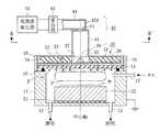
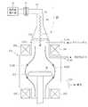
図1は、本発明の第1の実施の形態である高周波プラズマ処理装置の構成を示す図である。このプラズマ処理装置は、半導体やLCDなどの基板(被処理体)Wを収容しこの基板Wに対してプラズマ処理を施す処理容器11と、この処理容器11内に高周波電磁界Fを供給しその作用により処理容器11内にプラズマPを生成するスロットアンテナの一種であるRLSA30と、このRLSA30に高周波電磁界を円偏波給電する給電部40とを有している。
【0016】
処理容器11は、上部が開口した有底円筒形をしている。この処理容器11の底面中央部には絶縁板21を介して載置台22が固定されている。この載置台22の上面に基板Wが配置される。
処理容器11の底面周縁部には、真空排気用の排気口12が設けられている。処理容器11の側壁には、処理容器11内にガスを導入するためのガス導入用ノズル13が設けられている。例えばこのプラズマ処理装置がエッチング装置として用いられる場合、ノズル13からArなどのプラズマガスと、CF4などのエッチングガスとが導入される。
【0017】
処理容器11の上部開口は、そこから高周波電磁界Fを導入しつつ、プラズマPを外部に漏らさないように、誘電体板14で閉塞されている。なお、処理容器11の側壁上面と誘電体板14との間にOリングなどのシール部材15を介在させ、処理容器11内の気密性を確保している。
誘電体板14の上にRLSA30が配設されている。誘電体板14およびRLSA30の外周は、処理容器11の側壁上に環状に配置されたシールド材16によって覆われ、高周波電磁界Fが外部に漏れない構造になっている。
【0018】
RLSA30は、ラジアル導波路33を形成する対向配置された2つの円形導体板31,32と、これら2つの導体板31,32の外周部を接続してシールドする導体リング34とから構成されている。
ラジアル導波路33の上面となる導体板(第4の導体板)32の中心部には、円形の開口35が形成され、この開口35を介して給電部40からラジアル導波路33内に高周波電磁界が導入される。ラジアル導波路33の下面となる導体板(第3の導体板)31には、ラジアル導波路33内を伝搬する高周波電磁界Fを処理容器11内に供給するスロット36が複数形成されている。
【0019】
ラジアル導波路33内には、アルミナなど比誘電率が1より大きい誘電体からなる遅波材37が配置されている。遅波材37によりラジアル導波路33の管内波長λg1が短くなるので、導体板31の半径方向に配置するスロット36を増やし、高周波電磁界Fの供給効率を向上させることができる。なお、遅波材37は必ずしも必要ではなく、装着しなくてもよい。
また、導体板31の中心部には、金属または誘電体で形成されたバンプ38が設けられている。このバンプ38は、導体板32の開口35に向かって突出する略円錐形に形成された部材である。バンプ38により、供給部40からラジアル導波路33へのインピーダンスの変化を緩やかにし、供給部40とラジアル導波路33との接続部での高周波電磁界の反射を低減することができる。
【0020】
給電部40は、RLSA30の開口35に一端が接続された円筒導波管41と、この円筒導波管41の他端にクロススロット51を介して接続された一端が閉じられた矩形導波管42と、この矩形導波管42の他端に接続された高周波発生器43と、矩形導波管42に設けられた負荷整合器44とを有している。
高周波発生器43は、周波数が1GHz〜十数GHzの範囲内の所定周波数の高周波電磁界を発生させ、出力するものである。なお、高周波発生器43は、マイクロ波帯およびそれより低い周波数帯を含む高周波を出力するものであってもよい。以下では2.45GHzの高周波電磁界を出力するものとして説明を続ける。
【0021】
負荷整合器44は、電源(高周波発生器43)側と負荷(RLSA30)側とのインピーダンスの整合をとるものである。インピーダンス整合をとることにより、高周波発生器43からRLSA30に高周波電磁界を効率よく供給することができる。なお、負荷整合器44を矩形導波管42に設ける代わりに、円筒導波管41に設けてもよい。
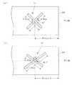
クロススロット51は、円筒導波管41に高周波電磁界を円偏波として、すなわち進行方向に対し垂直な面内で1周期で1回転する回転電磁界として供給する円偏波アンテナとして作用する。以下、図1および図2を参照し、クロススロット51の構成について、詳しく説明する。図2は、クロススロット51の構成例を示す平面図であり、矩形導波管42のE面をII−II′線方向から見た図である。
【0022】
図2(a)に示すクロススロット51は、矩形導波管42のE面における円筒導波管41との接続部分に形成されている。このクロススロット51は、互いに長さが異なる2本のスロットが互いの中心で交差した構成をしている。これら2本のスロットそれぞれの中心、すなわちクロススロット51の中心は、E面の略中心軸上にある。また、矩形導波管42の終端42Aは金属で閉じられており、この終端42Aから略λg2/2だけ離れた位置にクロススロット51の中心が配置される。λg2は、矩形導波管42内の管内波長である。この位置にクロススロット51を配置することにより、クロススロット51による放射電界の振幅を最大にすることができる。
【0023】
クロススロット51を構成する2本のスロットは、2.45GHzに対する周波数特性が相対的に55゜〜70゜程度異なり、各スロットによる放射電界の振幅が等しくなるように、各スロットの長さおよび角度が調整される。
具体的には、2本のスロットの長さを、それぞれ5.57cm、6.06cmとすると共に、その2本のスロットを互いに略直角に交差させ、矩形導波管42のE面の中心軸に対して略45゜傾斜するように配置することができる。
また、図2(b)に示すように、2本のスロットの長さを、それぞれ5.32cm、7.26cmとすると共に、その2本のスロットを互いに略107゜の角度で交差させ、矩形導波管42のE面の中心軸に対して略36.5゜傾斜するように配置してもよい。
【0024】
このようなクロススロット51を矩形導波管42のE面に形成することにより、2.45GHzの周波数に対して軸比が極めて1に近いTE11モードの円偏波が得られる。ここに軸比とは、円偏波の円形断面上の電界強度分布(時間平均)における最大値と最小値との比をいう。
【0025】
次に、図1に示したプラズマ処理装置の動作について説明する。
高周波発生器43で発生した高周波電磁界は、矩形導波管42をTE10モードで伝搬し、E面に形成されたクロススロット51から円筒導波管41内に放射される。円筒導波管41内に放射された高周波電磁界はTE11モードの円偏波となり、回転電磁界が生成される。この回転電磁界が、円筒導波管41から開口35を介してRLSA30内に導入されることにより、RLSA30に対して円偏波給電が行われる。
RLSA30に導入された高周波電磁界は、RLSA30に複数形成されたスロット36から誘電体板14を介して処理容器11内に供給される。処理容器11内に供給された高周波電磁界は、ノズル13を通じて処理容器11内に導入されたプラズマガスを電離させてプラズマPを生成し、基板4に対する処理が行われる。
【0026】
このように、図1に示したプラズマ処理装置は、矩形導波管42のE面に形成されたクロススロット51により、高周波電磁界を円筒導波管41内に回転電磁界として供給することができるので、円筒導波管541内の高周波電磁界を回転電磁界に変換するために従来用いられていた円偏波変換器591が不要となる。したがって、円偏波変換器591がもたらした問題を解消し、円偏波給電を行なってプラズマPを生成する動作を安定化させると共に、長時間の連続稼動を可能にすることができる。
また、円偏波変換器591だけでなく、矩形円筒変換器592も不要となるので、部品点数を削減し、プラズマ処理装置の製造コストを低減することができる。
【0027】
(第2の実施の形態)
図3は、本発明の第2の実施の形態である高周波プラズマ処理装置の一部の構成を示す図である。この図には、給電部の構成を示しているが、図1と同一部分または相当部分を同一符号で示しており、その説明を適宜省略する。
図1に示した給電部40では、クロススロット51が矩形導波管42のE面に形成されているのに対し、この図3に示した給電部40Aでは、クロススロット53が矩形導波管45の終端面に形成されている点で異なっている。以下、図3および図4を参照し、この相違点を中心に説明する。
【0028】
図4は、矩形導波管45の終端面に形成されるクロススロット53の構成例を示す平面図であり、矩形導波管45の終端面をIV−IV′線方向から見た図である。クロススロット53の構成は、E面に形成されるクロススロット51の構成と概ね同じである。すなわち、クロススロット53は、互いに長さが異なる2本のスロットが互いの中心で交差した構成をし、これら2本のスロットは、2.45GHzに対する周波数特性が相対的に55゜〜70゜程度異なり、各スロットによる放射電界の振幅が等しくなるように調整されている。具体的には、2本のスロットの長さを、それぞれ5.57cm、6.06cmとすると共に、その2本のスロットを互いに略直角に交差させ、矩形導波管45の中心部に生成される仮想的な電界線に対して略45゜傾斜するように配置することができる。ただし、クロススロット53の中心は、矩形導波管45の終端面の略中心に配置される。
【0029】
このようなクロススロット53を矩形導波管45の終端面に形成することにより、2.45GHzの周波数に対して軸比が極めて1に近いTE11モードの円偏波が得られる。
したがって、図3に示した給電部40Aは、矩形導波管45の終端面に形成されたクロススロット53により、高周波電磁界を円筒導波管41内に回転電磁界として供給することができるので、図1に示した給電部40と同じく円偏波変換器591が不要となり、その結果、円偏波給電を行なってプラズマPを生成する動作を安定化させると共に、長時間の連続稼動を可能にすることができる。
【0030】
なお、本発明の第1,第2の実施の形態では、クロススロット51,53を用いる例を示したが、図5に示すように、互いに略垂直な方向の2本のスロット55A,55Bを離間して配置した所謂ハの字スロットを用いて円筒導波管41に円偏波を供給するようにしてもよい。ハの字スロットは、一方のスロット55Aの延長線が、他方のスロット55B上またはその延長線上で交差するものであればよい。
また、クロススロット51,53またはハの字スロットを構成するスロットの平面形状は、図6(a)に示すような矩形であってもよいし、図6(b)に示すような平行な二直線の両端を円弧などの曲線でつないだ形状であってもよい。スロットの長さLとは、図6(a)では矩形の長辺の長さであり、図6(b)では平行な二直線の長さである。
【0031】
(第3の実施の形態)
図7は、本発明の第3の実施の形態である高周波プラズマ処理装置の一部の構成を示す図である。この図には、給電部の構成を示しているが、図1と同一部分または相当部分を同一符号で示しており、その説明を適宜省略する。
図7に示した給電部は、パッチアンテナ71を用いて高周波電磁界を円筒導波管41内に回転電磁界として供給するものである。パッチアンテナ71は、円筒導波管41の他端を閉じる接地された円形導体板41Aと、この円形導体板41Aの下面に配置された誘電体板72と、この誘電体板72を介して円形導体板41Aに対向配置された導体板73とから構成されている。以下では、円形導体板41Aと導体板73との混同を避けるため、前者を地板41A、後者を共振器73と呼ぶ。
【0032】
地板41Aには、2本の同軸導波管61,62の外部導体61A,62A(外部導体62Aは図示せず)が接続され、共振器73には、2本の同軸導波管61,62の内部導体61B,62B(内部導体62Bは図示せず)が接続されている。共振器73の中心を接地電位に固定するために、共振器73の中心を導体柱で地板41Aに接続してもよい。地板41A、共振器73および導体柱は、銅又はアルミニウムなどにより形成され、誘電体板72はセラミックなどにより形成される。
【0033】
図8は、共振器73をVIII−VIII′線方向から見たときの平面図である。共振器73の平面形状は、一辺が略λg3/2の正方形をしている。λg3は、地板41Aと共振器73との間を伝播する高周波電磁界の波長である。
共振器73の中心を座標系の原点Oとし、共振器73の各辺と平行にx軸,y軸を設定すると、2本の同軸導波管61,62の内部導体61B,62Bは、共振器73上の原点Oから略等距離にあるx軸,y軸上の2点に接続される。この2点を給電点S,Tと呼ぶ。
【0034】
このような構成のパッチアンテナ71に対して、2本の同軸導波管61,62から等振幅かつ位相が互いに90゜異なる高周波電磁界を給電することにより、円筒導波管41内にTE11モードの回転電磁界を生成することができる。その原理は次のとおりである。
共振器73のx軸方向の長さはλg3/2であるから、一方の同軸導波管61より給電点Sに供給された電流はx軸方向で共振し、共振器73のy軸に平行な二辺からx軸に平行な直線偏波が放射される。また、共振器73のy軸方向の長さもλg3/2であるから、他方の同軸導波管62より給電点Tに供給された電流はy軸方向で共振し、共振器73のx軸に平行な二辺からy軸に平行な直線偏波が放射される。2本の同軸導波管61,62による給電位相は互いに90゜異なるので、放射される2つの直線偏波の位相も互いに90゜異なっている。しかも両者は振幅が等しく、空間的に直交しているので、円偏波となり、円筒導波管41に回転電磁界が生成される。
【0035】
このように、図7に示した給電部は、パッチアンテナ71により高周波電磁界を円筒導波管41内に回転電磁界として供給することができるので、図1に示した給電部40と同じく円偏波変換器591が不要となり、その結果、円偏波給電を行なってプラズマPを生成する動作を安定化させると共に、長時間の連続稼動を可能にすることができる。
【0036】
なお、パッチアンテナ71への給電位相の差を90°とするには、移相器を用いてもよいが、互いの電気長が90°異なる2つの同軸導波管に同位相の高周波電磁界を供給するようにしてもよい。
また、パッチアンテナ71が有する共振器73の平面形状は、図8に示した正方形の他、円形などの90°回転対称形状(共振器73をその面内で90゜回転させたときに重なる形状)であってもよい。ただし、円形の場合には、直径を略1.17×λg3/2とするとよい。さらにまた、共振器73の平面形状は、長方形など、その中心からみた直交する2方向の長さが異なる形状であってもよい。この場合、2つの給電点S,Tにおける給電位相の差を90°とはせず、上記2方向の長さによって調整する。
【0037】
(第4の実施の形態)
図9は、本発明の第4の実施の形態である高周波プラズマ処理装置の一部の構成を示す図である。この図には、給電部の構成を示しているが、図1および図7と同一部分または相当部分を同一符号で示しており、その説明を適宜省略する。図7に示した給電部は、2本の同軸導波管61,62を用いた二点給電のパッチアンテナ71を用いているのに対し、この図9に示した給電部、1本の同軸導波管61を用いた一点給電のパッチアンテナ75を用いている点で異なっている。以下、この相違点を中心に説明する。
【0038】
パッチアンテナ75は、円筒導波管41の他端を閉じる接地された円形導体板41Aと、この円形導体板41Aの下面に配置された誘電体板72と、この誘電体板72を介して円形導体板41Aに対向配置された導体板76とから構成されている。以下では、円形導体板41Aと導体板76との混同を避けるため、前者を地板41A、後者を共振器76と呼ぶ。地板41Aには同軸導波管61の外部導体61Aが接続され、共振器76には同軸導波管61の内部導体61Bが接続されている。
【0039】
図10は、共振器76をX−X′線方向から見たときの平面図である。この図に示すように、共振器76の平面形状は、円76Aの周縁領域の一部を切り欠いた形状をしている。より詳しく言うと、円周とy軸とが交差する付近の2領域を矩形状に切り欠いた形状をしている。切り欠き面積は円76Aの面積の3%程度とするとよい。ここでは、共振器76のx軸方向の長さを略1.17×λg3/2とし、y軸方向の長さを略1.17×λg3/2−2dとする。
同軸導波管61の内部導体61Bは、x軸,y軸と45゜の角度で交差する直線上の一点に接続されている。この点を給電点Uと呼ぶ。
【0040】
同軸導波管61より共振器76の給電点Uに供給された電流は、x軸方向およびy軸方向にそれぞれ独立に流れる。このとき、y軸方向の長さは1.17×λg3/2よりも2dだけ短いので、電磁界からみた誘電率が大きくなり、y軸方向を流れる電流の位相が遅れる。この位相遅れが90゜となるように2dの値と切り欠き部の長さが設定されれば、パッチアンテナ75から円偏波が放射され、円筒導波管41内にTE11モードの回転電磁界が生成される。
このように、図9に示した給電部は、パッチアンテナ75により高周波電磁界を円筒導波管41内に回転電磁界として供給することができるので、図1または図7に示した給電部と同じく円偏波変換器591が不要となり、その結果、円偏波給電を行なってプラズマPを生成する動作を安定化させると共に、長時間の連続稼動を可能にすることができる。
【0041】
なお、共振器76の平面形状は図10に示した形状に限られるものではなく、少なくとも共振器76の中心からみた直交する二方向の長さが異なる形状であればよい。したがって、例えば楕円形であってもよいし、長辺の長さがおよそλg3/2であり、短辺の長さがおよそλg3/2未満である矩形であってもよい。
【0042】
(第5の実施の形態)
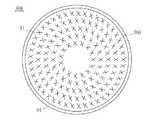
図11は、本発明の第5の実施の形態である高周波プラズマ処理装置の一部の構成を示す図である。この図には、RLSAのスロット配置を示しているが、図1と同一部分または相当部分を同一符号で示しており、その説明を適宜省略する。
【0043】
本発明の第1〜第4の実施の形態では、処理容器11内に高周波電磁界Fを供給するスロットアンテナとしてRLSA30を用いているが、クロススロット36Aを配置したRLSA30Aを用いてもよい。クロススロット36Aの構成は、図1,図2に示した給電部40で用いられるクロススロット51と同様でよい。すなわち、クロススロット36Aは、互いに長さが異なる2本のスロットが互いの中心で交差した構成をしている。ただし、遅波材37の作用でRLSA30Aの管内波長λg1が矩形導波管42の管内波長λg2より短いので、それに応じてクロススロット36Aの寸法も小さくなっている。
【0044】
図11に示したRLSA30Aでは、このようなクロススロット36Aが、スロット面を構成する導体板31上に同心円上に複数配置されている。同心円の間隔(内側の円と外側の円との半径の差)は、RLSA30Aの管内波長λg2と等しくてもよいが、これに限定されるものではない。なお、クロススロット36Aが渦巻線上に複数配置されていてもよい。渦巻線の間隔(渦巻線上を1回転したときの半径方向の変位)も、上記同心円の間隔と同様である。
クロススロット36Aには、それを構成する2本のスロットが交差する点で円偏波が得られるので、設計どおりの円偏波が容易に得られるという特徴がある。よって、このようなクロススロット36Aを複数配置したRLSA30Aを用いることにより、処理容器11内に円偏波を設計どおりに放射することができる。これにより、処理容器11内の電界強度分布を時間平均で軸対称な分布とし、その電磁界の作用により均一性のよいプラズマPを生成することができる。
【0045】
なお、RLSA30,30Aは、スロット面を構成する導体板31が平板状であるが、図12および図13(a)に示すRLSA30Bのように、スロット面を構成する導体板31Aが円錐面状をしていてもよい。円錐面状をしたスロット面から放射(またはリーク)される高周波電磁界Fは、平板状をした誘電体板14によって規定されるプラズマ面に対して斜め方向から入射されることになる。このため、プラズマPによる高周波電磁界Fの吸収効率が向上するので、アンテナ面とプラズマ面との間に存在する定在波を弱め、プラズマ分布の均一性を向上させることができる。
なお、RLSA30Bのアンテナ面を構成する導体板31Aは、上に凸の円錐面状をしているが、図13(b)に示すように下に凸の円錐面状をした導体板31Bを用いることもできる。また、導体板31A,31Bは、円錐面状以外の凸形状であってもよい。
【0046】
(第6の実施の形態)
本発明は上述した高周波プラズマ処理装置だけでなく、ECRプラズマ処理装置にも適用することができる。図14は、本発明の第6の実施の形態であるECRプラズマ処理装置の一構成例を示す図である。図14において、図1および図2と同一部分または相当部分を同一符号で示しており、その説明を適宜省略する。
【0047】
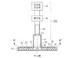
図14に示すECRプラズマ処理装置は、プラズマが生成されるプラズマ室111Aと、プラズマCVDなどの処理が行われる反応室111Bとからなる処理容器111を有している。
プラズマ室111Aの外周には、プラズマ室111A内に磁束密度Bが87.5mTの磁界を形成する主電磁コイル181が設けられている。プラズマ室111Aの上端には、誘電体板114を介して給電部140が接続され、この給電部140から電子サイクロトロン振動数(プラズマ中の電子が磁力線を中心に回転運動するときの振動数)2.45GHzと同じ振動数の高周波電磁界Fが供給される。
【0048】
プラズマ室111Aと連通する反応室111Bの内部には、半導体やLCDなどの基板(被処理体)Wを上面に載置する載置台122が収容されている。また、反応室111Bの底面の下には、補助電磁コイル182が設けられている。主電磁コイル181と補助電磁コイル182とからなる磁界発生器により、反応室111B内にミラー磁界MMが形成される。
また、プラズマ室111Aの上部には、例えばN2 などのプラズマガスを供給するノズル113Aが設けられ、反応室111Bの上部には、例えばSiH4 などの反応性ガスを供給するノズル113Bが設けられている。さらに、反応室111Bの下部には、真空ポンプに連通する排気口112が設けられている。
【0049】
このような構成において、プラズマ室111A内に磁束密度Bが87.5mTの磁界を形成するとともに、振動数が2.45GHzの高周波電磁界Fを導入すると、電子サイクロトロン共鳴が起こり、高周波電磁界Fのエネルギーが電子に効率よく移行し電子が加熱される。このようにして高周波電磁界Fで加熱された電子により、プラズマ室111A内のN2の電離が続けられ、プラズマが生成される。
【0050】
一方、給電部140は、図1に示した給電部40と同様の構成を有している。すわなち給電部140は、誘電体板114を介してプラズマ室111Aの上端に一端が接続された円筒導波管41と、この円筒導波管41の他端にクロススロット51を介して接続された矩形導波管42と、この矩形導波管42の他端に接続された高周波発生器43と、矩形導波管42に設けられた負荷整合器44とを有している。なお、給電部140として、図3、図7または図9に示した給電部を用いてもよい。
【0051】
これらの給電部では、円筒導波管41内に高周波電磁界を回転電磁界として供給することができるので、円筒導波管541内の高周波電磁界を回転電磁界に変換するために従来用いられていた円偏波変換器591が不要となる。したがって、円偏波変換器591がもたらした問題を解消し、円偏波給電を行なってプラズマを生成する動作を安定化させると共に、長時間の連続稼動を可能にすることができる。
また、円偏波変換器591だけでなく、矩形円筒変換器592も不要となるので、部品点数を削減し、プラズマ処理装置の製造コストを低減することができる。
【0052】
なお、本発明のプラズマ処理装置は、エッチング装置、CVD装置、アッシング装置などに利用することができる。
【0053】
【発明の効果】
以上説明したように、本発明では、スロットアンテナに高周波電磁界を供給する給電部が、スロットアンテナに対して開口する円筒導波管と、この円筒導波管に高周波電磁界を回転電磁界として供給する円偏波アンテナとを有している。このため、円筒導波管内の高周波電磁界を回転電磁界に変換するための円偏波変換器を設ける必要がない。したがって、円偏波変換器がもたらした問題を解消し、円偏波給電を行なってプラズマを生成する動作を安定化させると共に、長時間の連続稼動を可能にすることができる。
【0054】
また、スロットアンテナから処理容器内に円偏波を放射する場合、スロットアンテナにクロススロットを複数形成することにより、円偏波を設計どおりに放射することができる。これにより、処理容器内の電界強度分布を時間平均で軸対称な分布とし、その電磁界の作用により均一性のよいプラズマを生成することができる。
また、スロットアンテナにバンプを設けることにより、円筒導波管からスロットアンテナへのインピーダンス変化を緩和し、円筒導波管とスロットアンテナとの接続部での高周波電磁界の反射を低減することができる。これにより、処理容器内に効率よく高周波電磁界を供給し、プラズマの生成効率を向上させることができる。
【0055】
また、本発明では、処理容器内にECR条件を満たす高周波電磁界を供給する給電部が、処理容器に対して開口する円筒導波管と、この円筒導波管に高周波電磁界を回転電磁界として供給する円偏波アンテナとを有している場合には、円筒導波管内の高周波電磁界を回転電磁界に変換するための円偏波変換器を設ける必要がない。したがって、円偏波変換器がもたらした問題を解消し、円偏波給電を行なってプラズマを生成する動作を安定化させると共に、長時間の連続稼動を可能にすることができる。
【図面の簡単な説明】
【図1】 本発明の第1の実施の形態である高周波プラズマ処理装置の構成を示す図である。
【図2】 給電部が有するクロススロットの構成例を示す平面図である。
【図3】 本発明の第2の実施の形態である高周波プラズマ処理装置の一部の構成を示す図である。
【図4】 給電部が有するクロススロットの構成例を示す平面図である。
【図5】 クロススロットに代替可能なハの字スロットの配置を示す図である。
【図6】 スロットの形状を示す平面図である。
【図7】 本発明の第3の実施の形態である高周波プラズマ処理装置の一部の構成を示す図である。
【図8】 給電部が有するパッチアンテナの共振器の平面図である。
【図9】 本発明の第4の実施の形態である高周波プラズマ処理装置の一部の構成を示す図である。
【図10】 給電部が有するパッチアンテナの共振器の平面図である。
【図11】 本発明の第5の実施の形態である高周波プラズマ処理装置の一部の構成を示す図である。
【図12】 本発明で使用可能なラジアルラインスロットアンテナの構成を示す断面図である。
【図13】 図12に示したラジアルラインスロットアンテナのスロット面の構成を示す斜視図である。
【図14】 本発明の第6の実施の形態であるECRプラズマ処理装置の一構成例を示す図である。
【図15】 円偏波給電方式を採用するプラズマ処理装置の給電部の従来構成を示す図である。
【図16】 円偏波変換器の構成例を示す図である。
【符号の説明】
11…処理容器、30…ラジアルラインスロットアンテナ(RLSA)、31…円形導体板(第3の導体板)、32…円形導体板(第4の導体板)、35…開口、36…スロット、36A…クロススロット、38…バンプ、40,40A,140…給電部、41…円筒導波管、41A…地板(第1の導体板)、42,45…矩形導波管、51,53…クロススロット(円偏波アンテナ)、55A,55B…スロット、61…同軸導波管、61A…外導体、61B…内導体、71…パッチアンテナ(円偏波アンテナ)、73…共振器(第2の導体板)、111…容器、181,182…電磁コイル(磁界発生部)、F…高周波電磁界。[0001]
BACKGROUND OF THE INVENTION
The present invention relates to a plasma processing apparatus and a plasma generation method.
Specifically, the present invention relates to a plasma processing apparatus and a plasma generation method for generating plasma by an electromagnetic field supplied into a processing container using a slot antenna.
The present invention also relates to a plasma processing apparatus and a plasma generation method for generating plasma using electrons heated by electron cyclotron-resonance (ECR).
[0002]
[Prior art]
In the manufacture of semiconductor devices and flat panel displays, plasma processing apparatuses are frequently used to perform processes such as oxide film formation, semiconductor layer crystal growth, etching, and ashing. One of these plasma processing apparatuses supplies a high-frequency electromagnetic field into the processing container using a slot antenna, and ionizes and dissociates the gas in the processing container by the action of the electromagnetic field to generate plasma. There is a device. Since this high-frequency plasma processing apparatus can generate high-density plasma at a low pressure, efficient plasma processing is possible.
[0003]
As a high-frequency plasma processing apparatus, there is a method of feeding circularly polarized waves to a slot antenna through a cylindrical waveguide. Circular polarization refers to an electromagnetic wave whose electric field vector is a rotating electric field that rotates once in one cycle in a plane perpendicular to the traveling direction. Therefore, due to the circular polarization feeding, the electric field strength distribution of the slot antenna becomes axisymmetric with respect to the axis of the traveling direction of the circular polarization on a time average. For this reason, it is possible to supply a high-frequency electromagnetic field having a time-averaged axially symmetrical distribution from the slot antenna into the processing vessel, and to generate plasma with good uniformity by the action of the electromagnetic field.
[0004]
FIG. 15 is a diagram illustrating a conventional configuration of a power feeding unit of a plasma processing apparatus that employs a circularly polarized power feeding method. This feeding unit feeds circularly polarized waves to a radial line slot antenna (hereinafter abbreviated as RLSA) 530, which is a kind of slot antenna, and a
[0005]
As the circularly
[0006]
Further, as the circularly
[0007]
[Problems to be solved by the invention]
However, when large power is applied, in the circularly polarized
Further, the circularly polarized
Since these problems occur when the circularly
[0008]
The present invention has been made to solve such problems, and an object of the present invention is to stabilize the operation of a plasma processing apparatus that performs circularly polarized power feeding.
Another object is to extend the continuous operation time of a plasma processing apparatus that performs circular polarization feeding.
[0009]
[Means for Solving the Problems]
In order to achieve such an object, a plasma processing apparatus according to the present invention includes a slot antenna that supplies a high-frequency electromagnetic field into a processing container in which a mounting table on which an object to be processed is placed, and a high-frequency power to the slot antenna. A plasma processing apparatus including a power feeding unit that supplies an electromagnetic field, wherein the power feeding unit is provided at one end of the cylindrical waveguide having an opening with respect to the slot antenna, and at the other end of the cylindrical waveguide. It has at least a circularly polarized antenna that supplies an electromagnetic field as a rotating electromagnetic field that rotates in a plane perpendicular to its traveling direction.
Further, the plasma processing apparatus of the present invention includes a magnetic field generation unit that forms a magnetic field in the processing container, and a power supply unit that supplies a high-frequency electromagnetic field in the processing container, and uses electrons heated by electron cyclotron resonance. A plasma processing apparatus for generating plasma, wherein a power feeding unit is provided at one end of a cylindrical waveguide having an opening with respect to a processing container, and the other end of the cylindrical waveguide, and a high-frequency electromagnetic field is moved in a traveling direction thereof. And at least a circularly polarized antenna supplied as a rotating electromagnetic field rotating in a plane perpendicular to the surface.
Since these plasma processing apparatuses have a circularly polarized antenna in which the power supply unit supplies a high-frequency electromagnetic field as a rotating electromagnetic field, a circular polarization for converting the high-frequency electromagnetic field in the cylindrical waveguide into a rotating electromagnetic field is provided. There is no need to provide a wave converter.
[0010]
In these plasma processing apparatuses, the power supply unit further includes a rectangular waveguide having one side connected to the other end of the cylindrical waveguide, and the circularly polarized antenna has a cylindrical waveguide on one side of the rectangular waveguide. It is good also as a structure which consists of 1 or several slot opened in the wave tube. Here, one side of the rectangular waveguide may be an E plane. Here, the E plane means a plane on which a virtual electric field line is emitted / incident in a rectangular waveguide.
In the plasma processing apparatus described above, the power feeding unit further includes a rectangular waveguide having a termination surface connected to the other end of the cylindrical waveguide, and the circularly polarized antenna has a termination surface of the rectangular waveguide. 1 may be configured by one or a plurality of slots opened in the cylindrical waveguide.
Here, the slots may be two slots having different lengths and intersecting each other at the center. The slots may be two slots that are spaced apart from each other and extend in directions substantially perpendicular to each other.
[0011]
Further, in the plasma processing apparatus described above, the power feeding section includes an inner conductor and an outer conductor disposed coaxially around the inner conductor, and at least one coaxial waveguide that feeds a high-frequency electromagnetic field to the circularly polarized antenna. The circularly polarized antenna further includes a first conductor plate that closes the other end of the cylindrical waveguide and is connected to the outer conductor of the coaxial waveguide, and a first conductor plate in the cylindrical waveguide. It is good also as a structure which is a patch antenna which has the 2nd conductor board connected to the inner conductor of a coaxial waveguide, spaced apart and opposed to the inner conductor.
[0012]
In the plasma processing apparatus described above, the slot antenna may be formed with a slot that radiates circularly polarized waves. By radiating circularly polarized waves from the slot antenna into the processing container, the electric field strength distribution in the processing container can be axisymmetric with respect to time average.
For example, the slot antenna may be formed with a plurality of cross slots in which two slots having different lengths intersect each other at the center. In the cross slot, circular polarization can be obtained at a point where two slots constituting the cross slot intersect, so that circular polarization as designed can be easily obtained.
[0013]
Further, in the plasma processing apparatus described above, the slot antenna is disposed opposite to the mounting table, the third conductor plate in which a plurality of slots are formed, the opposite end to the third conductor plate, and one end of the cylindrical waveguide. It is good also as a structure which has the 4th conductor board which has an opening to which is connected, and the bump which is arrange | positioned on the 3rd conductor board and protrudes toward the opening of a 4th conductor board. By providing the bumps, the impedance change from the cylindrical waveguide to the slot antenna can be mitigated.
[0014]
The plasma generation method of the present invention is a plasma generation method for generating plasma in a processing container by supplying a high frequency electromagnetic field to a slot antenna and supplying the slot antenna to the processing container. A high-frequency electromagnetic field is supplied into the wave tube as a rotating electromagnetic field that rotates in a plane perpendicular to its traveling direction, and is supplied from the cylindrical waveguide to the slot antenna.
The plasma generation method of the present invention is a plasma generation method for generating a plasma using electrons heated by electron cyclotron resonance by forming a magnetic field in a processing vessel and supplying a high-frequency electromagnetic field. A high-frequency electromagnetic field is supplied into the wave tube as a rotating electromagnetic field that rotates in a plane perpendicular to its traveling direction, and is supplied from the cylindrical waveguide into the processing vessel.
[0015]
DETAILED DESCRIPTION OF THE INVENTION
Hereinafter, embodiments of the present invention will be described in detail with reference to the drawings.
(First embodiment)
FIG. 1 is a diagram showing a configuration of a high-frequency plasma processing apparatus according to the first embodiment of the present invention. The plasma processing apparatus accommodates a substrate (object to be processed) W such as a semiconductor or an LCD and performs plasma processing on the substrate W, and supplies a high frequency electromagnetic field F into the
[0016]
The
An
[0017]
The upper opening of the
An
[0018]
The
A
[0019]
In the
A
[0020]
The
The
[0021]
The
The
[0022]
The
[0023]
The length and angle of each of the two slots constituting the
Specifically, the lengths of the two slots are set to 5.57 cm and 6.06 cm, respectively, and the two slots intersect with each other at a substantially right angle, so that the central axis of the E plane of the
Further, as shown in FIG. 2B, the lengths of the two slots are set to 5.32 cm and 7.26 cm, respectively, and the two slots are intersected with each other at an angle of approximately 107 ° to form a rectangular shape. You may arrange | position so that it may incline about 36.5 degrees with respect to the center axis | shaft of the E surface of the
[0024]
By forming such a
[0025]
Next, the operation of the plasma processing apparatus shown in FIG. 1 will be described.
The high frequency electromagnetic field generated by the
The high frequency electromagnetic field introduced into the
[0026]
As described above, the plasma processing apparatus shown in FIG. 1 can supply a high-frequency electromagnetic field as a rotating electromagnetic field into the
Further, since not only the circularly polarized
[0027]
(Second Embodiment)
FIG. 3 is a diagram showing a partial configuration of the high-frequency plasma processing apparatus according to the second embodiment of the present invention. Although the configuration of the power feeding unit is shown in this figure, the same or corresponding parts as those in FIG.
In the
[0028]
FIG. 4 is a plan view showing a configuration example of the
[0029]
By forming such a
Therefore, the
[0030]
In the first and second embodiments of the present invention, the example in which the
Further, the planar shape of the slots constituting the
[0031]
(Third embodiment)
FIG. 7 is a diagram showing a partial configuration of a high-frequency plasma processing apparatus according to the third embodiment of the present invention. Although the configuration of the power feeding unit is shown in this figure, the same or corresponding parts as those in FIG.
The power feeding unit shown in FIG. 7 supplies a high-frequency electromagnetic field as a rotating electromagnetic field into the
[0032]
The
[0033]
FIG. 8 is a plan view of the
When the center of the
[0034]
The
The length of the
[0035]
7 can supply a high-frequency electromagnetic field as a rotating electromagnetic field into the
[0036]
Note that a phase shifter may be used in order to set the difference in the feeding phase to the
The planar shape of the
[0037]
(Fourth embodiment)
FIG. 9 is a diagram showing a partial configuration of a high-frequency plasma processing apparatus according to the fourth embodiment of the present invention. In this figure, the configuration of the power feeding unit is shown, but the same or corresponding parts as those in FIGS. 1 and 7 are denoted by the same reference numerals, and description thereof will be omitted as appropriate. The feed unit shown in FIG. 7 uses a two-point
[0038]
The
[0039]
FIG. 10 is a plan view of the
The
[0040]
The current supplied from the
9 can supply a high-frequency electromagnetic field as a rotating electromagnetic field into the
[0041]
Note that the planar shape of the
[0042]
(Fifth embodiment)
FIG. 11 is a diagram showing a partial configuration of a high-frequency plasma processing apparatus according to the fifth embodiment of the present invention. This figure shows the slot arrangement of the RLSA, but the same or corresponding parts as those in FIG. 1 are indicated by the same reference numerals, and the description thereof is omitted as appropriate.
[0043]
In the first to fourth embodiments of the present invention, the
[0044]
In the
The
[0045]
In the
The
[0046]
(Sixth embodiment)
The present invention can be applied not only to the high-frequency plasma processing apparatus described above but also to an ECR plasma processing apparatus. FIG. 14 is a diagram showing a configuration example of an ECR plasma processing apparatus according to the sixth embodiment of the present invention. In FIG. 14, the same or corresponding parts as those in FIGS. 1 and 2 are denoted by the same reference numerals, and description thereof will be omitted as appropriate.
[0047]
The ECR plasma processing apparatus shown in FIG. 14 includes a
A main
[0048]
In the
Further, an upper portion of the
[0049]
In such a configuration, when a magnetic field having a magnetic flux density B of 87.5 mT is formed in the
[0050]
On the other hand, the power feeding unit 140 has the same configuration as that of the
[0051]
These power supply units can supply a high-frequency electromagnetic field as a rotating electromagnetic field into the
Further, since not only the circularly polarized
[0052]
The plasma processing apparatus of the present invention can be used for an etching apparatus, a CVD apparatus, an ashing apparatus, and the like.
[0053]
【The invention's effect】
As described above, in the present invention, the power feeding unit that supplies a high-frequency electromagnetic field to the slot antenna has a cylindrical waveguide that opens to the slot antenna, and the high-frequency electromagnetic field is used as a rotating electromagnetic field in the cylindrical waveguide. And a circularly polarized antenna to be supplied. For this reason, it is not necessary to provide a circularly polarized wave converter for converting the high-frequency electromagnetic field in the cylindrical waveguide into a rotating electromagnetic field. Therefore, the problem caused by the circularly polarized wave converter can be solved, the operation of generating plasma by performing circularly polarized power feeding can be stabilized, and continuous operation for a long time can be enabled.
[0054]
In addition, when circularly polarized waves are radiated from the slot antenna into the processing container, circularly polarized waves can be radiated as designed by forming a plurality of cross slots in the slot antenna. As a result, the electric field strength distribution in the processing vessel is axisymmetric with respect to time average, and plasma with good uniformity can be generated by the action of the electromagnetic field.
Also, by providing bumps on the slot antenna, the impedance change from the cylindrical waveguide to the slot antenna can be mitigated, and the reflection of high-frequency electromagnetic fields at the connection between the cylindrical waveguide and the slot antenna can be reduced. . Thereby, the high frequency electromagnetic field can be efficiently supplied into the processing container, and the plasma generation efficiency can be improved.
[0055]
In the present invention, the power feeding unit that supplies the high-frequency electromagnetic field that satisfies the ECR condition in the processing container includes a cylindrical waveguide that opens to the processing container, and the high-frequency electromagnetic field is transmitted to the cylindrical waveguide by the rotating electromagnetic field. In the case of having a circularly polarized antenna to be supplied as a circularly polarized wave antenna, there is no need to provide a circularly polarized wave converter for converting the high frequency electromagnetic field in the cylindrical waveguide into a rotating electromagnetic field. Therefore, the problem caused by the circularly polarized wave converter can be solved, the operation of generating plasma by performing circularly polarized power feeding can be stabilized, and continuous operation for a long time can be enabled.
[Brief description of the drawings]
FIG. 1 is a diagram showing a configuration of a high-frequency plasma processing apparatus according to a first embodiment of the present invention.
FIG. 2 is a plan view illustrating a configuration example of a cross slot included in a power feeding unit.
FIG. 3 is a diagram showing a partial configuration of a high-frequency plasma processing apparatus according to a second embodiment of the present invention.
FIG. 4 is a plan view illustrating a configuration example of a cross slot included in a power feeding unit.
FIG. 5 is a diagram showing an arrangement of a C-shaped slot that can be substituted for a cross slot.
FIG. 6 is a plan view showing the shape of a slot.
FIG. 7 is a diagram showing a partial configuration of a high-frequency plasma processing apparatus according to a third embodiment of the present invention.
FIG. 8 is a plan view of a resonator of a patch antenna included in a power feeding unit.
FIG. 9 is a diagram showing a partial configuration of a high-frequency plasma processing apparatus according to a fourth embodiment of the present invention.
FIG. 10 is a plan view of a patch antenna resonator included in the power feeding unit.
FIG. 11 is a diagram showing a partial configuration of a high-frequency plasma processing apparatus according to a fifth embodiment of the present invention.
FIG. 12 is a cross-sectional view showing a configuration of a radial line slot antenna that can be used in the present invention.
13 is a perspective view showing a configuration of a slot surface of the radial line slot antenna shown in FIG. 12. FIG.
FIG. 14 is a diagram showing a configuration example of an ECR plasma processing apparatus according to a sixth embodiment of the present invention.
FIG. 15 is a diagram illustrating a conventional configuration of a power feeding unit of a plasma processing apparatus that employs a circularly polarized power feeding method.
FIG. 16 is a diagram illustrating a configuration example of a circular polarization converter.
[Explanation of symbols]
DESCRIPTION OF
Claims (6)
Translated fromJapanese前記給電部は、
一端が前記スロットアンテナに対して開口する円筒導波管と、
この円筒導波管の他端に接続された矩形導波管と、
この矩形導波管に設けられ、前記高周波電磁界をその進行方向に対し垂直な面内で回転する回転電磁界として前記円筒導波管内に供給する円偏波アンテナと
を少なくとも有し、
前記矩形導波管は、前記円筒導波管の前記他端に一側面が接続され、
前記円偏波アンテナは、前記矩形導波管の一側面において前記円筒導波管内に開口した1つまたは複数のスロットから構成され、
前記スロットは、互いの長さが異なり、互いの中心で交差する2本のスロットである
ことを特徴とするプラズマ処理装置。A plasma processing apparatus comprising: a slot antenna that is accommodated in a processing container that accommodates an object to be processed, and that supplies a high-frequency electromagnetic field to the processing container; ,
The power feeding unit is
A cylindrical waveguide having one end open to the slot antenna;
A rectangular waveguide connected to the other end of the cylindrical waveguide;
This provided a rectangular waveguide, the high frequency electromagnetic field to atleast have a and circularly polarized antenna supplied to the cylindrical waveguide as a rotating electromagnetic field that rotates in a plane perpendicular to the traveling directionthereof,
The rectangular waveguide has one side connected to the other end of the cylindrical waveguide,
The circularly polarized antenna is composed of one or more slots opened in the cylindrical waveguide on one side of the rectangular waveguide,
2. The plasma processing apparatus according toclaim 1, wherein the slots are two slots having different lengths and intersecting each other at the center .
前記給電部は、
一端が前記処理容器に対して開口する円筒導波管と、
この円筒導波管の他端に接続された矩形導波管と、
この矩形導波管に設けられ、前記高周波電磁界をその進行方向に対し垂直な面内で回転する回転電磁界として前記円筒導波管内に供給する円偏波アンテナと
を少なくとも有し、
前記矩形導波管は、前記円筒導波管の前記他端に一側面が接続され、
前記円偏波アンテナは、前記矩形導波管の一側面において前記円筒導波管内に開口した1つまたは複数のスロットから構成され、
前記スロットは、互いの長さが異なり、互いの中心で交差する2本のスロットである
ことを特徴とするプラズマ処理装置。A plasma processing apparatus that includes a magnetic field generation unit that forms a magnetic field in a processing container and a power feeding unit that supplies a high-frequency electromagnetic field in the processing container, and generates plasma using electrons heated by electron cyclotron resonance. And
The power feeding unit is
A cylindrical waveguide having one end open to the processing vessel;
A rectangular waveguide connected to the other end of the cylindrical waveguide;
This provided a rectangular waveguide, the high frequency electromagnetic field to atleast have a and circularly polarized antenna supplied to the cylindrical waveguide as a rotating electromagnetic field that rotates in a plane perpendicular to the traveling directionthereof,
The rectangular waveguide has one side connected to the other end of the cylindrical waveguide,
The circularly polarized antenna is composed of one or more slots opened in the cylindrical waveguide on one side of the rectangular waveguide,
2. The plasma processing apparatus according toclaim 1, wherein the slots are two slots having different lengths and intersecting each other at the center .
前記矩形導波管の前記一側面は、E面であることを特徴とするプラズマ処理装置。In the plasma processing apparatus according to claim 1 or 2,
The plasma processing apparatus, wherein the one side surface of the rectangular waveguide is an E surface .
前記給電部は、
一端が前記スロットアンテナに対して開口する円筒導波管と、
この円筒導波管の他端に接続された矩形導波管と、
この矩形導波管に設けられ、前記高周波電磁界をその進行方向に対し垂直な面内で回転する回転電磁界として前記円筒導波管内に供給する円偏波アンテナと
を少なくとも有し、
前記給電部は、前記円筒導波管の前記他端に、終端面が接続された矩形導波管を更に有し、
前記円偏波アンテナは、前記矩形導波管の終端面において前記円筒導波管内に開口した1つまたは複数のスロットから構成され、
前記スロットは、互いの長さが異なり、互いの中心で交差する2本のスロットである
ことを特徴とするプラズマ処理装置。A plasma processing apparatus comprising: a slot antenna that is accommodated in a processing container that accommodates an object to be processed, and that supplies a high-frequency electromagnetic field to the processing container; ,
The power feeding unit is
A cylindrical waveguide having one end open to the slot antenna;
A rectangular waveguide connected to the other end of the cylindrical waveguide;
A circularly polarized antenna provided in the rectangular waveguide and supplying the high-frequency electromagnetic field into the cylindrical waveguide as a rotating electromagnetic field rotating in a plane perpendicular to the traveling direction thereof;
Having at least
The power feeding unit further includes a rectangular waveguide having a termination surface connected to the other end of the cylindrical waveguide,
The circularly polarized antenna is composed of one or a plurality of slots opened in the cylindrical waveguide at the end face of the rectangular waveguide;
2. The plasma processing apparatus according toclaim 1, wherein the slots are two slots having different lengths and intersecting each other at the center .
前記給電部は、
一端が前記処理容器に対して開口する円筒導波管と、
この円筒導波管の他端に接続された矩形導波管と、
この矩形導波管に設けられ、前記高周波電磁界をその進行方向に対し垂直な面内で回転する回転電磁界として前記円筒導波管内に供給する円偏波アンテナと
を少なくとも有し、
前記給電部は、前記円筒導波管の前記他端に、終端面が接続された矩形導波管を更に有し、
前記円偏波アンテナは、前記矩形導波管の終端面において前記円筒導波管内に開口した1つまたは複数のスロットから構成され、
前記スロットは、互いの長さが異なり、互いの中心で交差する2本のスロットである
ことを特徴とするプラズマ処理装置。A plasma processing apparatus that includes a magnetic field generation unit that forms a magnetic field in a processing container and a power feeding unit that supplies a high-frequency electromagnetic field in the processing container, and generates plasma using electrons heated by electron cyclotron resonance. And
The power feeding unit is
A cylindrical waveguide having one end open to the processing vessel;
A rectangular waveguide connected to the other end of the cylindrical waveguide;
A circularly polarized antenna provided in the rectangular waveguide and supplying the high-frequency electromagnetic field into the cylindrical waveguide as a rotating electromagnetic field rotating in a plane perpendicular to the traveling direction thereof;
Having at least
The power feeding unit further includes a rectangular waveguide having a termination surface connected to the other end of the cylindrical waveguide,
The circularly polarized antenna is composed of one or a plurality of slots opened in the cylindrical waveguide at the end face of the rectangular waveguide;
2. The plasma processing apparatus according toclaim 1, wherein the slots are two slots having different lengths and intersecting each other at the center .
前記給電部は、
一端が前記スロットアンテナに対して開口する円筒導波管と、
この円筒導波管の他端に接続された矩形導波管と、
この矩形導波管に設けられ、前記高周波電磁界をその進行方向に対し垂直な面内で回転する回転電磁界として前記円筒導波管内に供給する円偏波アンテナと
を少なくとも有し、
前記スロットアンテナには、互いの長さが異なる2本のスロットが互いの中心で交差するクロススロットが複数形成されている
ことを特徴とするプラズマ処理装置。A plasma processing apparatus comprising: a slot antenna that is accommodated in a processing container that accommodates an object to be processed, and that supplies a high-frequency electromagnetic field to the processing container; ,
The power feeding unit is
A cylindrical waveguide having one end open to the slot antenna;
A rectangular waveguide connected to the other end of the cylindrical waveguide;
A circularly polarized antenna provided in the rectangular waveguide and supplying the high-frequency electromagnetic field into the cylindrical waveguide as a rotating electromagnetic field rotating in a plane perpendicular to the traveling direction thereof;
Having at least
2. The plasma processing apparatus accordingto claim 1, wherein the slot antenna is formed with a plurality of cross slots in which two slots having different lengths intersect each other at the center .
Priority Applications (4)
| Application Number | Priority Date | Filing Date | Title |
|---|---|---|---|
| JP2001385999AJP4209612B2 (en) | 2001-12-19 | 2001-12-19 | Plasma processing equipment |
| PCT/JP2002/013246WO2003052806A1 (en) | 2001-12-19 | 2002-12-18 | Plasma treatment apparatus and plasma generation method |
| US10/498,056US7305934B2 (en) | 2001-12-19 | 2002-12-18 | Plasma treatment apparatus and plasma generation method |
| AU2002357601AAU2002357601A1 (en) | 2001-12-19 | 2002-12-18 | Plasma treatment apparatus and plasma generation method |
Applications Claiming Priority (1)
| Application Number | Priority Date | Filing Date | Title |
|---|---|---|---|
| JP2001385999AJP4209612B2 (en) | 2001-12-19 | 2001-12-19 | Plasma processing equipment |
Publications (2)
| Publication Number | Publication Date |
|---|---|
| JP2003188152A JP2003188152A (en) | 2003-07-04 |
| JP4209612B2true JP4209612B2 (en) | 2009-01-14 |
Family
ID=19187890
Family Applications (1)
| Application Number | Title | Priority Date | Filing Date |
|---|---|---|---|
| JP2001385999AExpired - Fee RelatedJP4209612B2 (en) | 2001-12-19 | 2001-12-19 | Plasma processing equipment |
Country Status (4)
| Country | Link |
|---|---|
| US (1) | US7305934B2 (en) |
| JP (1) | JP4209612B2 (en) |
| AU (1) | AU2002357601A1 (en) |
| WO (1) | WO2003052806A1 (en) |
Families Citing this family (19)
| Publication number | Priority date | Publication date | Assignee | Title |
|---|---|---|---|---|
| KR100871465B1 (en)* | 2003-02-13 | 2008-12-03 | 도쿄엘렉트론가부시키가이샤 | Method for manufacturing semiconductor device and forming silicon oxide film, and apparatus for manufacturing semiconductor device |
| JP3974553B2 (en)* | 2003-05-07 | 2007-09-12 | 東京エレクトロン株式会社 | Plasma processing apparatus, antenna for plasma processing apparatus, and plasma processing method |
| WO2005088763A1 (en)* | 2004-03-10 | 2005-09-22 | Tokyo Electron Limited | Distributor and distributing method, plasma processing system and method, and process for fabricating lcd |
| JP4149427B2 (en)* | 2004-10-07 | 2008-09-10 | 東京エレクトロン株式会社 | Microwave plasma processing equipment |
| JP4576291B2 (en) | 2005-06-06 | 2010-11-04 | 株式会社日立ハイテクノロジーズ | Plasma processing equipment |
| WO2009041629A1 (en)* | 2007-09-28 | 2009-04-02 | Tokyo Electron Limited | Plasma processing device |
| JP5189999B2 (en)* | 2009-01-29 | 2013-04-24 | 東京エレクトロン株式会社 | Microwave plasma processing apparatus and microwave power supply method for microwave plasma processing apparatus |
| US8980047B2 (en)* | 2010-07-02 | 2015-03-17 | Samsung Electronics Co., Ltd. | Microwave plasma processing apparatus |
| EP2450823B1 (en)* | 2010-11-04 | 2013-07-17 | Keba Ag | detecting a foreign body in the vicinity of a means of input used for authentification |
| CN103476878B (en) | 2010-12-08 | 2015-09-16 | 黑达乐格瑞菲工业有限公司 | Preparation of granular materials, composite materials including granular materials and their applications |
| KR101332337B1 (en) | 2012-06-29 | 2013-11-22 | 태원전기산업 (주) | Microwave lighting lamp apparatus |
| US9660314B1 (en)* | 2013-07-24 | 2017-05-23 | Hrl Laboratories, Llc | High efficiency plasma tunable antenna and plasma tuned delay line phaser shifter |
| JP5805227B2 (en)* | 2014-01-28 | 2015-11-04 | 東京エレクトロン株式会社 | Plasma processing equipment |
| LU92947B1 (en)* | 2016-01-14 | 2017-08-07 | Iee Sa | Narrowband Leaky Wave Antenna for Sensing Objects in Relation to a Vehicle |
| JP2019192606A (en) | 2018-04-27 | 2019-10-31 | 東京エレクトロン株式会社 | Antenna apparatus and plasma processing apparatus |
| US10896811B2 (en) | 2018-08-30 | 2021-01-19 | Tokyo Electron Limited | Antenna device, radiation method of electromagnetic waves, plasma processing apparatus, and plasma processing method |
| WO2021220329A1 (en)* | 2020-04-27 | 2021-11-04 | 株式会社日立ハイテク | Plasma treatment device |
| WO2023032725A1 (en)* | 2021-09-03 | 2023-03-09 | 東京エレクトロン株式会社 | Plasma processing device and plasma control method |
| CN119999338A (en) | 2023-09-13 | 2025-05-13 | 株式会社日立高新技术 | Plasma treatment device |
Family Cites Families (10)
| Publication number | Priority date | Publication date | Assignee | Title |
|---|---|---|---|---|
| US3715688A (en)* | 1970-09-04 | 1973-02-06 | Rca Corp | Tm01 mode exciter and a multimode exciter using same |
| JPH04207703A (en)* | 1990-11-30 | 1992-07-29 | Inax Corp | Plane antenna |
| TW312815B (en) | 1995-12-15 | 1997-08-11 | Hitachi Ltd | |
| TW406280B (en)* | 1997-05-21 | 2000-09-21 | Fusion Lighting Inc | non-rotating electrodeless lamp containing molecular fill |
| JP3736054B2 (en) | 1997-07-15 | 2006-01-18 | 株式会社日立製作所 | Plasma processing equipment |
| JP3834958B2 (en)* | 1997-09-30 | 2006-10-18 | 株式会社日立製作所 | Plasma processing equipment |
| US6016766A (en)* | 1997-12-29 | 2000-01-25 | Lam Research Corporation | Microwave plasma processor |
| JP3496560B2 (en)* | 1999-03-12 | 2004-02-16 | 東京エレクトロン株式会社 | Plasma processing equipment |
| KR100789796B1 (en)* | 2000-03-30 | 2007-12-31 | 동경 엘렉트론 주식회사 | Plasma processing equipment |
| JP3893888B2 (en)* | 2001-03-19 | 2007-03-14 | 株式会社日立製作所 | Plasma processing equipment |
- 2001
- 2001-12-19JPJP2001385999Apatent/JP4209612B2/ennot_activeExpired - Fee Related
- 2002
- 2002-12-18AUAU2002357601Apatent/AU2002357601A1/ennot_activeAbandoned
- 2002-12-18WOPCT/JP2002/013246patent/WO2003052806A1/enactiveApplication Filing
- 2002-12-18USUS10/498,056patent/US7305934B2/ennot_activeExpired - Fee Related
Also Published As
| Publication number | Publication date |
|---|---|
| WO2003052806A1 (en) | 2003-06-26 |
| US7305934B2 (en) | 2007-12-11 |
| JP2003188152A (en) | 2003-07-04 |
| AU2002357601A1 (en) | 2003-06-30 |
| US20050082003A1 (en) | 2005-04-21 |
Similar Documents
| Publication | Publication Date | Title |
|---|---|---|
| JP4209612B2 (en) | Plasma processing equipment | |
| US7243610B2 (en) | Plasma device and plasma generating method | |
| JP5391209B2 (en) | Plasma processing equipment | |
| US6325018B1 (en) | Flat antenna having openings provided with conductive materials accommodated therein and plasma processing apparatus using the flat antenna | |
| JP3136054B2 (en) | Plasma processing equipment | |
| JP4837854B2 (en) | Matching device and plasma processing apparatus | |
| US20050162335A1 (en) | Plasma device | |
| JP2000235900A (en) | Plasma treatment device | |
| US20040244693A1 (en) | Electromagnetic field supply apparatus and plasma processing device | |
| JP4598253B2 (en) | Plasma device | |
| JP4499323B2 (en) | Electromagnetic field supply apparatus and plasma processing apparatus | |
| JP3914071B2 (en) | Plasma processing equipment | |
| JP3874726B2 (en) | Plasma processing apparatus and plasma generation method | |
| JP4658309B2 (en) | Plasma processing equipment | |
| JP4535356B2 (en) | Plasma device | |
| JP3736054B2 (en) | Plasma processing equipment | |
| JP4481538B2 (en) | Electromagnetic field supply apparatus and plasma processing apparatus | |
| JP4486068B2 (en) | Plasma generation method | |
| JP3899272B2 (en) | Plasma device | |
| JP2018006257A (en) | Microwave plasma processing device | |
| JP2002280367A (en) | Apparatus and method for plasma treatment | |
| JPH0719674B2 (en) | Electrode device of microwave discharge reactor | |
| JPH06325898A (en) | Microwave discharge reactor |
Legal Events
| Date | Code | Title | Description |
|---|---|---|---|
| A621 | Written request for application examination | Free format text:JAPANESE INTERMEDIATE CODE: A621 Effective date:20041217 | |
| A131 | Notification of reasons for refusal | Free format text:JAPANESE INTERMEDIATE CODE: A131 Effective date:20071127 | |
| A521 | Written amendment | Free format text:JAPANESE INTERMEDIATE CODE: A523 Effective date:20080128 | |
| A02 | Decision of refusal | Free format text:JAPANESE INTERMEDIATE CODE: A02 Effective date:20080513 | |
| A521 | Written amendment | Free format text:JAPANESE INTERMEDIATE CODE: A523 Effective date:20080612 | |
| A911 | Transfer to examiner for re-examination before appeal (zenchi) | Free format text:JAPANESE INTERMEDIATE CODE: A911 Effective date:20080718 | |
| TRDD | Decision of grant or rejection written | ||
| A01 | Written decision to grant a patent or to grant a registration (utility model) | Free format text:JAPANESE INTERMEDIATE CODE: A01 Effective date:20081021 | |
| A01 | Written decision to grant a patent or to grant a registration (utility model) | Free format text:JAPANESE INTERMEDIATE CODE: A01 | |
| A61 | First payment of annual fees (during grant procedure) | Free format text:JAPANESE INTERMEDIATE CODE: A61 Effective date:20081023 | |
| R150 | Certificate of patent or registration of utility model | Free format text:JAPANESE INTERMEDIATE CODE: R150 | |
| FPAY | Renewal fee payment (event date is renewal date of database) | Free format text:PAYMENT UNTIL: 20111031 Year of fee payment:3 | |
| FPAY | Renewal fee payment (event date is renewal date of database) | Free format text:PAYMENT UNTIL: 20111031 Year of fee payment:3 | |
| FPAY | Renewal fee payment (event date is renewal date of database) | Free format text:PAYMENT UNTIL: 20141031 Year of fee payment:6 | |
| LAPS | Cancellation because of no payment of annual fees |