JP4208258B2 - Method and apparatus for coating a workpiece - Google Patents
Method and apparatus for coating a workpieceDownload PDFInfo
- Publication number
- JP4208258B2 JP4208258B2JP53214497AJP53214497AJP4208258B2JP 4208258 B2JP4208258 B2JP 4208258B2JP 53214497 AJP53214497 AJP 53214497AJP 53214497 AJP53214497 AJP 53214497AJP 4208258 B2JP4208258 B2JP 4208258B2
- Authority
- JP
- Japan
- Prior art keywords
- workpiece
- chamber
- discharge
- cathode
- coating
- Prior art date
- Legal status (The legal status is an assumption and is not a legal conclusion. Google has not performed a legal analysis and makes no representation as to the accuracy of the status listed.)
- Expired - Fee Related
Links
Images


Classifications
- H—ELECTRICITY
- H01—ELECTRIC ELEMENTS
- H01J—ELECTRIC DISCHARGE TUBES OR DISCHARGE LAMPS
- H01J37/00—Discharge tubes with provision for introducing objects or material to be exposed to the discharge, e.g. for the purpose of examination or processing thereof
- H01J37/32—Gas-filled discharge tubes
- H—ELECTRICITY
- H01—ELECTRIC ELEMENTS
- H01J—ELECTRIC DISCHARGE TUBES OR DISCHARGE LAMPS
- H01J37/00—Discharge tubes with provision for introducing objects or material to be exposed to the discharge, e.g. for the purpose of examination or processing thereof
- H01J37/32—Gas-filled discharge tubes
- H01J37/32009—Arrangements for generation of plasma specially adapted for examination or treatment of objects, e.g. plasma sources
- H01J37/32055—Arc discharge
- C—CHEMISTRY; METALLURGY
- C23—COATING METALLIC MATERIAL; COATING MATERIAL WITH METALLIC MATERIAL; CHEMICAL SURFACE TREATMENT; DIFFUSION TREATMENT OF METALLIC MATERIAL; COATING BY VACUUM EVAPORATION, BY SPUTTERING, BY ION IMPLANTATION OR BY CHEMICAL VAPOUR DEPOSITION, IN GENERAL; INHIBITING CORROSION OF METALLIC MATERIAL OR INCRUSTATION IN GENERAL
- C23C—COATING METALLIC MATERIAL; COATING MATERIAL WITH METALLIC MATERIAL; SURFACE TREATMENT OF METALLIC MATERIAL BY DIFFUSION INTO THE SURFACE, BY CHEMICAL CONVERSION OR SUBSTITUTION; COATING BY VACUUM EVAPORATION, BY SPUTTERING, BY ION IMPLANTATION OR BY CHEMICAL VAPOUR DEPOSITION, IN GENERAL
- C23C14/00—Coating by vacuum evaporation, by sputtering or by ion implantation of the coating forming material
- C23C14/22—Coating by vacuum evaporation, by sputtering or by ion implantation of the coating forming material characterised by the process of coating
- C23C14/24—Vacuum evaporation
- C23C14/32—Vacuum evaporation by explosion; by evaporation and subsequent ionisation of the vapours, e.g. ion-plating
- C—CHEMISTRY; METALLURGY
- C23—COATING METALLIC MATERIAL; COATING MATERIAL WITH METALLIC MATERIAL; CHEMICAL SURFACE TREATMENT; DIFFUSION TREATMENT OF METALLIC MATERIAL; COATING BY VACUUM EVAPORATION, BY SPUTTERING, BY ION IMPLANTATION OR BY CHEMICAL VAPOUR DEPOSITION, IN GENERAL; INHIBITING CORROSION OF METALLIC MATERIAL OR INCRUSTATION IN GENERAL
- C23C—COATING METALLIC MATERIAL; COATING MATERIAL WITH METALLIC MATERIAL; SURFACE TREATMENT OF METALLIC MATERIAL BY DIFFUSION INTO THE SURFACE, BY CHEMICAL CONVERSION OR SUBSTITUTION; COATING BY VACUUM EVAPORATION, BY SPUTTERING, BY ION IMPLANTATION OR BY CHEMICAL VAPOUR DEPOSITION, IN GENERAL
- C23C14/00—Coating by vacuum evaporation, by sputtering or by ion implantation of the coating forming material
- C23C14/22—Coating by vacuum evaporation, by sputtering or by ion implantation of the coating forming material characterised by the process of coating
- C23C14/50—Substrate holders
- C23C14/505—Substrate holders for rotation of the substrates
Landscapes
- Chemical & Material Sciences (AREA)
- Engineering & Computer Science (AREA)
- Organic Chemistry (AREA)
- Materials Engineering (AREA)
- Mechanical Engineering (AREA)
- Metallurgy (AREA)
- Chemical Kinetics & Catalysis (AREA)
- Physics & Mathematics (AREA)
- Plasma & Fusion (AREA)
- Analytical Chemistry (AREA)
- Physical Vapour Deposition (AREA)
- Paints Or Removers (AREA)
- Coating By Spraying Or Casting (AREA)
- Application Of Or Painting With Fluid Materials (AREA)
Description
Translated fromJapaneseこの発明は、請求項1のプリアンブルに記載の被覆配置、ならびに請求項14のプリアンブルに記載の工作物を被覆するための方法に関するものである。
様々な真空処理プロセスにおいては、真空被覆を行う前に工作物表面を浄化することが知られている。さらに、工作物はこの浄化段階の前後に所望の温度に加熱され得る。そのような段階はとりわけ、後に蒸着されるべき層に優れた付着強さを付与するために、必要である。これは特に、工作物、特に工具が耐摩耗性を備えた硬質層で被覆されるべき適用例において、重要である。工具、例えばドリル、スライス、ブローチ、形削り工具等のそのような層は、特に高い機械的ストレスおよび研磨ストレスに晒される。したがって、基板との極めて優れた接合が、利用に耐え得る、効率使用の前提となる。そのような工作物に前処理を施す確かな方法としては、電子衝撃による加熱と、イオン・エッチングまたはスパッタ・エッチングによるエッチングとがある。プラズマ放電からの電子衝撃による加熱は、例えばDE 33 30 144によって周知のものとなった。プラズマ放電路はまた、例えばアルゴン・イオンのような重い不活性気体イオンを発生させるためにも使用される。このプラズマからのイオンは、工作物または基板に向けて促進されて、DE 28 23 876に記載されているように、そこでスパッタ・エッチングを行う。スパッタ・エッチングと並んで、さらなる反応性ガスによってプラズマ放電を行い、工作物を反応化学的にエッチングする方法もまた周知のものであるが、ここで、この反応性エッチングとスパッタ・エッチングとを混合することもまた可能である。これら全ての前処理工程は、その後の被覆が基板によく接合するように、工作物の表面を準備することをその目的とする。前述の配置においては、プラズマを発生させるために、低電圧アーク放電が装置の中心軸に配置され、工作物が一定の距離を置いてこのアークの周りに、円筒状表面に沿って配置される。続いて、熱蒸着またはスパッタによる被覆が行われる。ここで、プロセスの進行によっては、基板のしかるべきバイアスに従って更なるイオン衝撃が被覆中に発生するが、これはイオン鍍金という概念で知られている。この配置には、より低い粒子エネルギーで低電圧アーク放電から大きなイオン流を引き出すことが出来、従って工作物を慎重に加工することが出来る、という利点がある。いずれにせよ、均一で再現可能な結果を得るためには、工作物を放電に対して放射状に規定される区域内に配置せねばならず、かつそれを、通常は中央軸ならびにそれ自体の軸を中心に回転させねばならない、という欠点がある。さらに、許容され得る円筒状の加工帯域幅が比較的狭いために、加工可能な工作物の大きさが限定される一方、より多数の小さな工作物の一回あたりの工程量が限定され、その結果、この周知の配置の経済性は著しく限定される、という欠点もある。この限定は、加工室の中央を満たす低電圧アーク放電自体がある一定の広がりを必要とし、そのため、再現可能な優れた結果を維持するには、工作物を放電から離す必要があるため、加工室の中央空間の大部分が利用され得ないことに、起因する。
いわゆるダイオード放電を用いるスパッタ配置もまた周知のものである。そのようなダイオード放電は、1000ボルトまでの、またそれ以上の高い電圧で行われる。ダイオード・エッチング装置は、高度の要求を伴う適用例には向かないことが実証された。達成し得るエッチング率、すなわち効率が悪い一方で、この高電圧では、微細な基板に欠陥が生じる。したがって、特に三次元の加工を必要とする工作物、例えば工具等は、容易には処理し得ない。工具は例えば、その仕上げ段階を経て、種々の精緻な切断端縁を備えており、それらの端縁にそのような放電が集中すると、例えば過熱や、場合によっては機能端縁の損壊等の制御不可能な影響が、それらの精緻な端縁および先端に生じ得る。
特許明細書DE 41 25 365には、前述の問題を解決する試みが記載されている。この開示は、いわゆるアークまたは電弧蒸化によって被覆が行われることを前提とする。そのような蒸化器によってしっかりと接合する層を形成するためには、本来の被覆過程の前に、蒸化器自体の電弧が以下のように利用される。すなわち、電弧において発生したイオン、特に蒸化ターゲットから発生した金属イオンが、典型的には>500ボルト、通常は800から1000ボルトの領域の負の加速電圧を介して、工作物に付着するよりはむしろ飛散するように、工作物に向けて促進される。このエッチング過程の後、蒸化器はさらに被覆源として使用される。明細書には、アーク被覆技術を用いたこの通常の工程では、アーク蒸化技術によってしっかりと接合する層を形成するために、そのような高い電圧が必要である、と記されている。過熱または、工作物の不均一な質量分布もしくは微細な幾何学におけるエッチングの問題を避け得るために、電弧プラズマの他に、より高い電圧の補助放電路をさらに使用することがこの明細書では提案されている。この補助放電路は補助的な電離を引き起こし、アーク蒸化器電弧に連結される。さらなる直流源によって、プラズマからイオンが抽出され、工作物に向けて促進されるが、これらのイオンが所望のエッチング過程を行う。その他に、別の電源によって作動する、さらなる放電路を備える別の陽極が設けられ、効果を高める。さらに、アーク蒸化器はエッチング過程の間、オリフィスが閉じられた状態で作動するので、この過程の間、基板は蒸化器の直接的作用から保護され、基板におけるいわゆる液滴が回避される。ここに記された配置の欠点は、同様に高い電圧が必要とされ、かつ、達成可能な加工均質性を保つことが限られた範囲内においてのみ可能である、という点である。さらに、様々なプラズマ路が結合されるため、操作条件を調整する可能性が限られてくる。その他、この配置は複雑であるため、実用化および操作に費用がかかり、生産用装置の経済性という観点からして不利である。さらに、1000ボルト以上の高い電圧を使用すると、さらなる安全対策費用が必要となる。
従来技術によって知られているような装置は、より優れた加工品質を維持しながら大量に加工するには、条件付きでのみ適していると言える。1000mmまで、およびそれ以上の被覆幅を許容する規模の装置は、可能であるとしても、様々な問題点を抱えてのみ実現可能である。
この発明の課題は、従来技術の欠点を除去することであり、特に、多数の工作物または不均一な質量分布を有する個々の大きな工作物の微細構造を、所望の均一性を維持しながら、要求される高経済性を有する加工率で、しっかりとかたよりなく被覆することができる、被覆配置を提供し、かつ方法を提案することである。
これは、始めに述べられたような加工配置を前提とし、それを請求項1の特徴に従って形成し、かつ、請求項14の特徴による被覆方法によって達成される。
それによると、被覆されるべき工作物の表面は、高温陰極低電圧アーク放電配置として形成されたプラズマ供給源の傍らを、その放電路の直線状の広がりを横切るように搬送される。その際、工作物には負の電圧がかかっているので、アーク放電から抽出されたイオンが工作物に向けて促進され、スパッタ・エッチングが行われ、続いて、低電圧アーク放電と同じ側からの働きかけにより、工作物は被覆される。
この発明の被覆配置の好ましい実施例は、従属請求項2から13に記載され、この方法の好ましい実施例は請求項14から17に記載される。
高温陰極低電圧アーク放電配置がイオン供給源として用いられるエッチングが特に有利なのは、そのようなアーク放電装置は、<200ボルトの放電電圧で作動可能であり、高電圧エッチングの欠点が生じないためである。低電圧アーク放電エッチングは従って、工作物に極めて優しく、より大きな工作物における例えば切断端縁等の微細構造が、温度による過負荷によっても、またより高いイオン・エネルギー衝撃による端縁の切削によっても、損なわれることがない。30から200ボルト領域のDC、好ましくは30から120ボルトの比較的低めの許容放電電圧であっても、約20、30から約200、300アンペアまでの、好ましくは100から300アンペアまでの極めて高めの放電電流が可能である。これは、この放電形態によると、よりわずかなエネルギーで極めて高いイオン流の利用が可能であることを意味する。したがって、基板における加速電圧が比較的低くとも、高いイオン流が利用可能であるため、高いエッチング率が達成可能であり、しかもこれが、既に述べられたように、工作物を慎重に扱いながらも可能である。基板における抽出電圧ないし加速電圧は、−50ボルトから−300ボルトの領域、好ましくは−100ボルトから−200ボルトの領域である。工作物に引き寄せられたイオン流はここでは5から20アンペアの値に達し、好ましくは8から16アンペアの領域で加工される。単数または複数の工作物の加工幅はここでは1000mmまで可能である。しかしながら、装置に幾分費用をかければ、より大きな加工幅も可能である。達成可能な数値は、アーク放電の操作値の他に、工作物に対するその幾何学的配置にも依存し、また選択された動作圧力にも依存する。典型的な作動圧力は10-3mbarの領域であり、アーク放電の作動には処理ガスとして不活性気体が、好ましくは、例えばアルゴン等のような比較的重い不活性気体が使用される。
これまで低電圧アーク放電配置は回転対称で操作されていた。すなわち、アーク放電が中央に配置され、中央軸内にあるこのアーク放電の周りを工作物が回転していた。これには、アーク放電が中央に配置された回転対称性配置によると、エッチング過程の均一性および速度に関して最善の結果を得ることができる、という前提があった。しかしながら今や驚くべきことに、この発明による非対称性の配置の方が、上述の回転対称性配置より総じて本質的により有利であることがわかった。アーク放電を中央軸に備えた回転対称性配置においてはすなわち、大容量の工作物を中央に向けて格納するにはアーク放電自体による制限があった。さらにそのような工作物は、エッチング過程の後、エッチングされた工作物が室壁に配置された被覆源によって直ちに被覆され得るように、中央軸の周りを回転する他に、さらに自転しなければならない。このような方法によってのみ、エッチング過程および被覆過程における優れて均一な分布が十分に可能となる。また、回転対称性配置においては、工作物に対して一方の側面からのみアーク放電が露出される非対称性の配置における場合より、工作物のアーク放電からの距離がより決定的な意味を持つ。この発明の配置によると、大容量の工作物をさらに回転させることなくアーク放電の前を搬送することが可能であり、これによって、加工室の大きさを合理的な範囲内に留めることが可能である一方、より重い工作物の取り扱いを実質的に簡略化することができる。これは生産用装置においては、その経済性に大きな影響をもたらす。この発明による配置は大容量の工作物においてのみ利点を有するものではなく、大容量の工作物の代わりに、相当数のより小さな工作物を装填し、同時に処理することも可能である。この発明による配置のさらなる利点は、エッチング装置をもはや加工室の一部として一体的に形成する必要がないという点である。このエッチング装置は依然として加工室壁の領域内に配置されねばならないが、例えば細長く、より小さな放電室を介してその外壁に装着可能であり、その結果、加工室の形態に関しては、実質的により大きな自由が認められる。アーク放電と工作物の表面との間の間隔に関しても、この配置は本質的にあまり問題ないことが確認された。したがって、特に大きな工作物に見られるような、より大きな間隔の変動があっても、再現可能な結果を得ることができる。総じてアーク放電から抽出され得るイオン流は、従来と同様、有利な高い数値を示し、工作物に集約されて、所望の高いエッチング率を達成する。低電圧アーク放電またはプラズマ供給源を、加工室または処理区域から完全に分離することによってまた、この供給源の形態により大きな自由を与えることができ、その結果、放電装置が装置の中央軸にある一体型の回転対称性配置における場合より、供給源の構造を実質的により柔軟に、工程の諸要件に適合させることができる。
エッチング過程の後、しっかりと接合する層を付着させるには、同じ側面から作用するように、加工室壁の領域にもう一つの、または複数のさらなる蒸化供給源が設けられる。特に適しているのは、細長い低電圧アーク放電と同様に細長い領域にわたって、傍らを通る工作物を被覆するように配置可能な供給源である。これには、例えばスパッタ供給源またはアーク蒸化器供給源等が適している。いわゆる陰極放電蒸化器またはアーク蒸化器が特に適していることが分かったが、これは、これらの蒸化器と、その前のエッチング段階とによって、特に強固な層の形成が極めて効率的に可能であるからである。この配置によって得られたテスト工具は、前段階において高電圧エッチングが行なわれた周知のアーク蒸化層よりも、明らかに優れた、再現可能な数値の耐用性能を示した。例えば、スライス等の切断工具においては、耐用年数が少なくとも1.5倍改善された。極めて有利なケースでは、従来の技術に対して複数倍も改善された。さらに、極めて均一なエッチング分布が達成されたが、これは部分的幾何学には実質的に、より依存せず、かつ一工程量につき極めて様々な基板の混合を可能にする。その他、提案された配置においては、不活性気体の他に、化学的に活性の気体を用いても容易にプロセスを実現することが可能である。これは、低電圧アーク放電が、例えばN2やH2等の活性ガスを極めてよく活性化するからである。絶縁表面を介して発生する望ましくない寄生放電は、低電圧アーク放電によって容易に抑制される。有利なことに、低電圧アーク放電は、高温の陰極を有し、かつ、小さな開口部を通してのみ放電室または加工室と接続された、独立した陰極室または電離室によって作動する。気体は、有利なことに、この陰極室を介して注入され、したがってプロセス室およびそれに関連する被覆供給源に対しては一定の気体分離が成立し、その結果、例えば被覆供給源における対象物の汚染の問題は軽減または回避される。この配置によってまた、本来の被覆段階の際、工作物において様々なプロセスガスを活性化することが可能となる。この際、工作物において負の電圧、場合によっては正の電圧を相応に選択することによって、所望の操作条件を選択的に調整することが可能である。
必要なエッチング深さ、または被覆厚さ、ならびに均一で再現可能な処理を達成するためには、通常、工作物を一つのプロセス段階につき複数回、供給源の前を通過させねばならないので、工作物が中央軸の周りを回転可能であり、かつ供給源は外側から内側に向けて同様に作用するように室壁の領域内に配置されるように、装置を形成するのが有利である。極めて大きな工作物は、例えばこのようにして中央軸内を回転するように配置され、加工され得る。しかしながらこの空間領域にはまた、多数のより小さな、しかも様々な大きさの工作物さえも保持具によって配置可能であり、この中央軸を中心に回転しながら供給源の傍らを搬送され、均一な結果をもたらすことが可能である。そのような配置は、簡単かつコンパクトに実現可能であり、より高い効率の操作を可能にする。
プラズマ供給源または低電圧アーク放電は、搬送方向を横断するように、加工室壁の領域内に直接配置されるのが有利である。低電圧アーク放電装置は例えば、好ましくはボックス状の付属装置に、ここでは放電室として、配置され得る。この放電室は、低電圧アークが単数または複数の工作物に、または加工されるべき区域に向けて直接晒されるように、放電に沿って、スリット状の開口部を介して加工室と接続される。低電圧アーク放電は、電気加熱された、または熱電子放出の陰極と、それから距離を置いた陽極とによって発生するが、陰極に対して、陽極に相応の放電電圧がかけられることによってアーク電流が引き出される。この放電室にはさらに、ガス流入配置が合流し、アーク放電に処理ガスを供給する。この配置は、例えばアルゴン等の不活性気体によって作動するのが好ましいが、既に述べられたように、反応性ガスもまた混合可能である。放電路は、処理区域幅にに対して少なくとも80%の広がりを有し、かつ、所望の処理分布または均一性が達成可能なように、処理区域に対して配置されるべきである。必要なスパッタ・エッチングを工作物において行うために、この工作物または工作物保持具は、アーク放電配置に対して負の電圧で動かされる。例えば被覆過程の間の反応性プロセス等における場合のように、この配置はそのような電圧なしでも、あるいは正の電圧、すなわち電子衝撃によっても、プロセスに応じて作動する。ここではまた、純粋なDC電圧の他に、例えば中間または高周波のAC交流電圧を用いることも可能であり、DCとACとの重ね合わせもまた可能である。DC電圧はまたパルス作動可能であり、また、その一部のみがパルス作動しながら重ね合わされる場合もあり得る。そのような供給によって、特定の反応プロセスの制御が可能である。とりわけ、誘電性区域が装置および工作物表面に存在する場合、または形成される場合にはまた、望ましくない寄生電弧の発生を妨げることができる。
加工区域における分布要件は、一方では放電の長さによって、他方ではその位置によって調整可能である。分布調整に関するもう一つのパラメータは、アーク放電に沿ったプラズマ密度の分布である。これには例えば、放電室の領域に配置されるさらなる磁場の助けによって影響を与えることができる。そのような場合には、放電室にそって配置された永久磁石によって調整および補正するのが望ましい。しかしながら、分布要件に応じて放電路に沿って配置され、かつそれぞれに独立して供給を受ける、さらなる陽極によって放電路が作動する場合、より好ましい結果が得られる。そのような配置によって、分布曲線を調整するある程度の可能性さえも得られる。放電路に沿った複数個の陽極を備える補正磁石を使用しない配置は、好ましい実施形態である。しかしながら、この好ましい実施形態と組み合わせて、補正のためにさらに2、3の磁石を用いることもまた可能である。追加陽極は、個々の陰極と共に容易に作動し得る。しかしながら、この電気回路を最適な状態で絶縁するためには、各陽極につきそれに相対する放出陰極を設けるのが有利であり、これによって、さらに良好な調整の可能性が保証される。
小さな開口部を介して放電室と接続される熱電子放出陰極が、独自の小さな陰極室内に配置されるのが好ましい。不活性気体注入配置は好ましくはこの陰極室に合流する。必要とあれば、この気体注入配置を介して活性ガスもまた注入され得る。しかしながら、活性ガスは好ましくは陰極室内へではなく、例えば放電室内に注入されるのがよい。電子は陰極室の開口部を介して、距離を置いた単数または複数の陽極に引き寄せられ、その際、電離気体は少なくとも部分的には、同様にこの開口部から排気される。加工室は、工作物がその周りを回転する中央軸が垂直に配置されるように、形成されるのが望ましい。ここでは、陰極または陰極室は好ましくは陽極の上部に配置される。陰極室においては、排気開口部は下方に向けて配置されるのが望ましい。この配置は、システム全体の処理を簡略化し、かつ粒子形成によって生じ得る諸問題を回避する助けとなる。
加工室は、低電圧アーク放電配置の他に少なくとももう一つの供給源を備え、この供給源はアーク蒸化器であるのが望ましい。これらの供給源は、同様に外側から中央軸または加工区域の方向に向けて放射状に作用する。低電圧アーク放電が搬送方向において被覆供給源の手前に配置されると有利である。アーク蒸化器は通常、全加工区域を所望の均一性をもって被覆できるように、アーク放電配置と同様、搬送方向を横切る直線状の広がりを有する。上述の被覆配置においては、所望の均一性が達成されるように室壁に分散配置された複数の丸いアーク蒸化器が使用されるのが望ましい。これは、蒸化器の優れた作動性能を分割することが可能である一方、分布をより適切に制御することが可能であり、ある一定の領域においては、電源を介して調整することさえ可能である、という利点を有する。これによって非常に高い加工率、従って高い経済性を達成することができる。ここで例として、工具、特に形削り工具の加工プロセスを以下に示す。
プロセス例
装置の配位配置は第2図および第3図のそれと同様である。工具はそれ自体の軸を中心に回転するのではなく、工具保持具がその中央軸の周りを回転することによって、ただ供給源の側を通過するだけである。ここでは、幅bが1000mmであり、直径Dが700mmである被覆区域が形成され、その内部に工具が配置される。装置室はここでは直径1200mm、高さ1300mmである。
エッチング・パラメータ
低電圧アーク電流 ILVA=200A
アーク放電電圧 ULVA=50V
アルゴン圧 PAr=2.0 x 10⁻³mbar
エッチング電圧 Usub=−200V
エッチング電流 Isub=12A
エッチング時間 t=30min
エッチング深さ 200nm
被覆:
各アーク蒸化器の電流 IARC=200A
(直径150mmのチタン・ターゲットを有する8個の蒸化器)
アーク放電電圧 UARC=20V
窒素圧 PN2=1.0 x 10⁻²mbar
バイアス電圧 UBias=−100V
被覆時間 t=45min
層の厚さ TiN 6μm
プロセスのサイクル時間は、過熱および冷却を含めて、一工程量の加工につき計150minである。
工作物における負の加速電圧のための電圧発生装置は通常、300ボルトDCまでの電圧で作動するが、工作物を保護するために、欠陥を出さずにより優れたエッチング率が可能な100から200ボルトの、より低い電圧領域で操作されるのが好ましい。低電圧アーク配置は、工作物から少なくとも10cm距離を置いて操作されねばならない。しかしながら、この距離は>15cmであるのが望ましく、その場合好ましくは、15から25cmであるべきである。これによって、より優れた分布を維持しながら、高い経済性が得られる。
この発明の被覆装置は特に、ドリル、スライスおよび形削り工具等の工具を加工するのに適している。従って、保持および搬送装置はこれらの工具を収容するのに適切なように形成される。上述の被覆配置によると、被覆されるべき部分が装置の中央軸の周りのみを移動しても、通常よい結果を得ることができる。しかしながら、特に限界に近い状態、すなわち極めて多数の小さな部品をこの装置に収容する場合、中央軸を中心とする回転の他に、各々この中央軸の周りを回転するさらなる回転軸を導入するという考えも容易に許容される。
次に、例として図面を参照に、この発明概略が説明される。
第1図は、従来技術による低電圧アーク放電を備える被覆配置を示す。
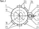
第2図は、低電圧アーク放電のための放電室が周辺部に装着された、この発明による被覆配置の実施例の断面図である。
第3図は、第2図の装置の水平断面図である。
第4a図は、同様に、複数の陽極配置がその中に装着された、低電圧アーク放電のための放電室を備える配置の、部分断面図である。
第4b図は、第4a図と同様の図であるが、ここではそれぞれに配置された陰極室を有する、分離された陰極および陽極放電路が示される。
第4c図は、第4a図および第4b図と同様の、分離された陰極および陽極放電路が示された図であるが、陰極が一つの共通陰極室に格納されている。
第5図は、従来技術およびこの発明に従って被覆された工具の、耐用年数比較曲線を示す。
第1図には、工作物のための周知の被覆配置が示される。真空室が低電圧アーク放電18を収容するための加工室1を形成し、低電圧アーク放電は、室1の中央においてその中央軸16に沿って延びる。室壁の周辺部には、加工室1の外側からマグネトロン・スパッタ供給源14がフランジを介して接合される。加工室1の上部側面には陰極室2が配置され、この陰極室は熱電子高温熱陰極3を収容し、ガス注入口5を介して処理ガス、典型的にはアルゴンのような不活性気体が供給され得る。しかしながら、反応性プロセスのためには活性ガスもまた混合され得る。陰極室2は、小さな開口部を備えるオリフィス4を介して加工室1と接続する。陰極室は通常、絶縁物6を介して加工室1と分離される。オリフィス4は、必要に応じて浮動電位または補助電位で操作され得るように、さらに絶縁物6を介して陰極室から分離される。陰極室2とは反対側の側面の中央軸方向16には陽極7が配置される。陽極7は、低電圧アーク放電によって蒸化され得る蒸化材料を収容するために坩堝状に形成される。しかしながら、エッチング過程の際にはこの蒸化手段は利用されず、ただ低電圧アーク放電からイオンが抽出され、工作物に向けて促進されることによって、工作物にスパッタ・エッチングが施される。低電圧アーク放電18を作動させるためには、陰極3がヒーター電流供給装置によって加熱され、電子を放出する。陰極3と陽極7との間には、アーク放電を作動させるためのさらなる電源装置8が設けられる。この電源装置8は通常、陽極7において正の直流電圧を発生させ、低電圧アーク18を維持する。アーク放電18と加工室1の室壁との間には、工作物を載せる保持具10が装着され、この装置は、十分なプロセスの均一性を達成し得るように、その垂直中央軸17の周りを回転し得る。さらに、これらの工作物保持具10はさらなる工作物保持配置12に載置される。この保持配置が工作物保持具10に中央軸16の周りを回転させるように、この配置12には回転駆動装置が設けられる。このタイプの装置においてはさらに、たとえばヘルツホルムコイル・タイプのさらなるコイル13を介して低電圧アーク放電18を集束することが必要である。ここで、工作物11が低電圧アーク放電18によって加工され得、かつ、負の電圧を基板に与えることによってイオン衝撃が生じ、正の基板電圧を与えることによって工作物の電子衝撃が可能であることは、明らかである。工作物にはこのようにして、一方では加熱による電子衝撃によって、また他方ではスパッタ・エッチングによるイオン衝撃によって、低電圧アーク放電の助けを得て前処理が施される。続いて、工作物11は坩堝7からの低電圧アークによる蒸化によって、あるいは電源15によって電力供給されるマグネトロン・スパッタ供給源14によるスパッタによって、被覆され得る。上記の配置においては、基板移動および低電圧アーク放電の配置のための機械的コストが大きいことが明白である。他方、工作物の配置が中央部の低電圧放電と外側の室壁の間においてのみ可能なので、自由度が大きく制限される。このような装置は、特に大きな工作物の場合、または一工程量が多い場合、経済的に作動させることができない。
この発明による好ましい被覆配置の例の断面図が第2図に示される。加工室1は、加工室lの中央軸16の周りを回転可能なように配置された、工作物11のための保持具を収容する。室は、通例どおり真空ポンプ19を介して排気され、この真空ポンプ19が加工プロセスに必要な動作圧力を維持する。提案された配置においては、例えば中央軸16を超えるような大きな工作物11は、この工作物11が加工室壁に配置された供給源によって加工され得る様に、加工室1内に配置される。基本的に加工室lの全域を装填に利用可能な区域が占める。したがって、そのような配置には個々の大きな工作物11だけでなく、基本的に室の全容積を占める、または利用し得る多数の工作物をも装填することが可能である。
工作物11を中央軸16の周りにおいて回転させる工作物保持具はしたがって、回転方向を横切る方向において被覆幅bを有する。この発明の配置は、一方では大きな被覆幅bにわたって、他方では中央軸16から加工幅の周辺部に至る広い深さ領域、すなわち全直径Dにおいて、均一で再現可能な加工結果を達成し得る、という点において特に有利である。これらの条件が難しい従来技術による従来の周知の同心性配置においては、上述の発明による偏心配置がもたらすようなより優れた結果は望めない。微細な端縁および切断面を有する工具の極めて多彩な幾何学は、この広い領域において、望ましくない温度負荷および望ましくない電弧の発生に関しては問題無く、制御可能である。
加工室外壁には、外側から工作物に向けて同様に作用するように、エッチングおよび被覆のための加工供給源が配置される。スパッタ・エッチングの重要な前処理段階のために、縦方向の広がりが少なくとも加工幅bに対応するスリット状の開口部が室壁に設けられる。この開口部26の後ろにはボックス状に形成された放電室21があり、この中で低電圧アーク放電18が発生する。この低電圧アーク放電は基本的に加工幅bに平行して延び、加工幅bの少なくとも80%にあたるべき有効長さlを有する。しかしながら、この放電の長さlは加工幅bに対応するか、あるいはこれと部分的に重なるのが望ましい。
アーク放電18の軸は、すぐ側の加工区域、すなわちすぐ側の工作物の部分との間に距離dを有するが、この距離は少なくとも10cm、好ましくは15から25cmであるべきである。これによって、加工の際に優れた均一性が得られる一方、高いスパッタ率が維持される。放電室21の下側部分には陰極室2がフランジによって接合され、この陰極室2はオリフィス4を介して放電室21と接続する。陰極室2は、ヒーター電源9によって電力供給される熱陰極3を内包する。この電力供給は交流または直流で行われ得る。陰極室2には、通常はアルゴンのような不活性ガスである処理ガスを、特定の反応プロセスのためには不活性ガスと活性ガスとの混合である処理ガスを供給するためのガス注入配置5が、合流する。さらに、処理ガスはまた加工室1を介しガス注入部22の助けを得て注入され得る。活性ガスは、ガス注入部22を介して直接加工室1内に注入されるのが望ましい。
放電室21の上部側面には陽極として形成された電極7が設けられる。陽極7が正極となり、したがって低電圧アーク放電が引き出され得るように、直流電流源8が陰極3と陽極7との間に接続される。低電圧アーク放電配置と工作物11との間の電圧発生装置20の助けを得て、負の電圧を工作物保持具または工作物11に与えることによって、アルゴン・イオンが工作物に促進され、表面がスパッタ・エッチングされる。これは、300ボルトDCまでの加速電圧によって行われ得るが、工作物11の慎重な加工を保証するためには、100ボルトから200ボルトの領域の値が選択されるのが望ましい。加工の均一性は、所望の条件に応じて、加工されるべき工作物11の加工幅bに対する陰極室2と陽極7との配置決めを各々相応に行うことによって、調整され得る。もう一つの要因は、陽極7の形状である。これは例えば、皿状、長方形等の平らな形状の電極として形成されるか、あるいは管状の冷却陽極として形成され得る。
第3図には、第2図による装置の水平断面図が示される。ここでも、加工室1の外壁に外側に折り返されたボックス状の放電室21が装着されており、スリット状の開口部26を介して処理区域と接続している。必要に応じて、例えば加工の効果をさらに高めるために、複数のそのような放電室が装置に配置され得ることは、自明である。さらに、室壁にフランジによって接合された蒸化供給源23が図示される。蒸化供給源23としては、例えばマグネトロン・スパッタ供給源が用いられるが、低コストで高い加工速度を維持するためには、いわゆるアーク蒸化供給源が使用されるのが望ましい。上記の配置の利点は、一方では、複数の供給源を分散して配置することによって所望の被覆均一性を調整することが可能なように、他方では、複数の供給源を用いることによって被覆率を高く保てるように、アーク蒸化供給源23を外側から自由に配置することができる、という点にある。ここでは、個々の長方形の蒸化供給源を使用するのではなく、複数のより小さな丸い供給源を、要求に応じて装置周辺部に分散して配置するほうが、より有利であることがわかった。
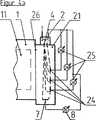
第4a図には、この発明の配置のもう一つの有利な形態が示される。ここでは、陰極室2が放電室21の上部側面に配置される。これには、そのような被覆装置に常に発生する粒子によって放電路の操作が妨げられるのが最小限で済む、という利点がある。さらに、複数の陽極および陰極電気回路を使用することによって、放電路を分割し、放電lに沿って強度を調整可能にする方法が示される。主要放電は、主要陽極7と陰極室2との間の電源8によって発生する。その他の補助放電は、補助陽極24と補助電源25とによって発生し得る。これによって、陽極7と陰極室2との間の全放電路における放電出力密度を、その場所および強度に関して、工作物の求める均一性の条件に適合させることが可能である。
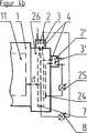
第4b図には、もう一つの調整方法が示される。別々の陽極7、24が利用されるだけでなく、別々の陰極3、3′および別々の陰極室2、2′が利用されることによって、陽極および陰極路が互いに完全に分離され、場合によっては絶縁され得る。もう一つの形態が示された第4c図では、二つの独立した陽極7、24が使用されるが、熱陰極3、3′を備える一つの共通陰極室2が利用される。
第5図には、一方はこの発明に従って処理され(曲線b)、もう一方は従来技術に従って処理された(曲線a)、HSS仕上げ削りスライスのテスト結果が示される。両方とも、スライスは3.5μm厚のTiNによって被覆された。従来技術によるスライス(曲線a)には周知のように、あらかじめ高電圧エッチングが施されたが、曲線bのスライスはこの発明による方法が適用された。テスト条件は以下のとおりである。
HSS仕上げ削りスライス: 直径16mm
歯の数: 4
テスト材料: 42 CrMo4 (DIN 1.7225)
硬度: HRC 38.5
送り込み: 15mm x 2.5mm
切断速度: 40m/min
各歯の送り: 0.088mm
送り: 280mm/min
耐用期間: 心棒トルク80(任意のユニット)
結果は、この発明に従って処理された工具における耐用年数の改善を明白に示している。1.5倍およびそれ以上の改善が容易に達成される。しかしながら、重要なのは耐用年数の延長だけではなく、耐用年数曲線の終了に向けて上昇するトルクまたは工具の品質劣化度の進行も、より平坦であるという点である。第5図の例によると、これは15mのスライス深さから顕著である。従来技術による曲線aは、15mのスライス深さで急激に折れ曲がる。これは、従来技術による切断品質は耐用年数全般にわたってより大きく変化する、すなわちあまり一定していないことを、意味する。
さらに、この発明による第2図から第4図の装置によると、例えば従来技術による第1図の装置に対して、上述の高い品質を保ちながら実質的により多量の処理が可能となる。ここでは、処理量の倍増は容易であり、3倍、5倍にすることさえ可能である。これによって経済性も劇的に高まる。The invention relates to a coating arrangement according to the preamble of
In various vacuum processing processes, it is known to clean the workpiece surface prior to vacuum coating. Furthermore, the workpiece can be heated to the desired temperature before and after this cleaning stage. Such a step is especially necessary in order to give excellent adhesion strength to the layer to be subsequently deposited. This is particularly important in applications where workpieces, in particular tools, are to be coated with a hard layer with wear resistance. Such layers of tools, such as drills, slices, broaches, shaping tools, etc. are exposed to particularly high mechanical and abrasive stresses. Therefore, extremely excellent bonding with the substrate is a prerequisite for efficient use that can withstand use. Certain methods of pretreating such workpieces include heating by electron impact and etching by ion etching or sputter etching. Heating by electron impact from a plasma discharge became known, for example, from
Sputtering arrangements using so-called diode discharge are also well known. Such diode discharge occurs at high voltages up to 1000 volts and above. Diode etchers have proven to be unsuitable for applications with high demands. While the achievable etch rate, i.e., efficiency, is poor, this high voltage causes defects in a fine substrate. Therefore, especially workpieces that require three-dimensional machining, such as tools, cannot be easily processed. The tool, for example, has various fine cutting edges after its finishing stage, and when such discharges are concentrated on those edges, for example, control of overheating, and possibly breakage of functional edges, etc. Impossible effects can occur on their fine edges and tips.
The patent specification DE 41 25 365 describes an attempt to solve the aforementioned problems. This disclosure assumes that the coating is performed by so-called arc or electric arc evaporation. In order to form a layer that is firmly joined by such an evaporator, the electric arc of the evaporator itself is used as follows before the actual coating process. That is, ions generated in the arc, especially metal ions generated from the evaporation target, are typically attached to the workpiece via a negative acceleration voltage in the region of> 500 volts, usually 800 to 1000 volts. Rather is encouraged towards the work piece to scatter. After this etching process, the evaporator is further used as a coating source. The specification states that in this normal process using the arc coating technique, such a high voltage is required to form a tightly bonded layer by the arc evaporation technique. In order to avoid overheating or etching problems in the uneven mass distribution or fine geometry of the workpiece, it is proposed in this document to additionally use a higher voltage auxiliary discharge path in addition to the arc plasma. Has been. This auxiliary discharge path causes auxiliary ionization and is connected to the arc evaporator arc. An additional DC source extracts ions from the plasma and promotes them towards the workpiece, but these ions perform the desired etching process. In addition, a separate anode with a further discharge path, operated by a separate power source, is provided to enhance the effect. Furthermore, since the arc evaporator operates with the orifice closed during the etching process, the substrate is protected from the direct action of the evaporator during this process and so-called droplets on the substrate are avoided. . The disadvantage of the arrangement described here is that a similarly high voltage is required and that it is only possible within a limited range to maintain achievable processing homogeneity. Furthermore, the possibility of adjusting the operating conditions is limited because the various plasma paths are coupled. In addition, since this arrangement is complicated, it is expensive to put into practical use and operation, which is disadvantageous from the viewpoint of economics of the production apparatus. In addition, the use of high voltages above 1000 volts requires additional safety measures.
It can be said that an apparatus as known from the prior art is only conditionally suitable for processing in large quantities while maintaining better processing quality. Equipment of a scale that allows a coating width of up to 1000 mm and beyond can be realized only with various problems, if possible.
The object of the present invention is to eliminate the disadvantages of the prior art, in particular a large number of workpieces or individual large workpiece microstructures having a non-uniform mass distribution, while maintaining the desired uniformity. It is to provide a coating arrangement and to propose a method which can be coated firmly and without difficulty at the required high economic processing rate.
This presupposes a processing arrangement as described at the outset, which is formed according to the features of
According to it, the surface of the workpiece to be coated is transported across a linear extension of its discharge path, beside a plasma source formed as a hot cathode low voltage arc discharge arrangement. At that time, since a negative voltage is applied to the workpiece, ions extracted from the arc discharge are promoted toward the workpiece, sputter etching is performed, and then from the same side as the low-voltage arc discharge. The work is covered by the action of.
Preferred embodiments of the coating arrangement according to the invention are described in the
Etching in which a hot cathode low voltage arc discharge arrangement is used as an ion source is particularly advantageous because such an arc discharge device can operate at a discharge voltage of <200 volts and does not suffer from the disadvantages of high voltage etching. is there. Low voltage arc discharge etching is therefore very gentle to the workpiece, and microstructures such as cutting edges in larger workpieces can be caused by temperature overloading and edge cutting by higher ion energy bombardment. It will not be damaged. Extremely high from about 20, 30 to about 200, 300 amps, preferably 100 to 300 amps, even at relatively low permissible discharge voltages in the 30 to 200 volt range, preferably 30 to 120 volts The discharge current is possible. This means that, according to this discharge mode, it is possible to use a very high ion flow with less energy. Therefore, high etching rates can be achieved because of the high ion flow available even at relatively low acceleration voltages on the substrate, and this can be done with careful handling of the workpiece, as already mentioned. It is. The extraction voltage or acceleration voltage at the substrate is in the region of -50 volts to -300 volts, preferably in the region of -100 volts to -200 volts. The ion stream attracted to the workpiece now reaches a value of 5 to 20 amperes and is preferably processed in the region of 8 to 16 amperes. The machining width of the workpiece or workpieces can here be up to 1000 mm. However, larger processing widths are possible if the equipment is somewhat expensive. The achievable numerical value depends not only on the arc discharge operating value, but also on its geometry relative to the workpiece and also on the selected operating pressure. Typical working pressure is 10-3 In the region of mbar, an inert gas is used as the process gas for the arc discharge operation, preferably a relatively heavy inert gas such as argon.
Until now, low voltage arcing arrangements have been operated rotationally symmetrically. That is, the arc discharge was placed in the center and the workpiece was rotating around this arc discharge in the central axis. This was based on the premise that the best results can be obtained with regard to the uniformity and speed of the etching process according to the rotationally symmetric arrangement with the arc discharge arranged in the center. However, it has now surprisingly been found that the asymmetric arrangement according to the invention is generally more advantageous than the rotationally symmetric arrangement described above. In a rotationally symmetric arrangement with an arc discharge at the central axis, that is, there is a limitation due to the arc discharge itself in storing a large-capacity workpiece toward the center. Furthermore, such a workpiece must rotate further in addition to rotating around the central axis so that after the etching process, the etched workpiece can be immediately coated by a coating source located on the chamber wall. Don't be. Only by such a method an excellent and uniform distribution in the etching and coating processes is sufficiently possible. Also, in the rotationally symmetric arrangement, the distance from the arc discharge of the workpiece is more decisive than in the asymmetric arrangement in which the arc discharge is exposed only from one side to the workpiece. According to the arrangement of the present invention, it is possible to transport a large-capacity workpiece before the arc discharge without further rotation, and thereby the size of the machining chamber can be kept within a reasonable range. On the other hand, handling of heavier workpieces can be substantially simplified. This has a great impact on the economics of production equipment. The arrangement according to the invention does not have an advantage only for large-capacity workpieces, it is also possible to load a considerable number of smaller workpieces and process them simultaneously instead of large-capacity workpieces. A further advantage of the arrangement according to the invention is that the etching device no longer has to be integrally formed as part of the processing chamber. This etching device still has to be placed in the region of the processing chamber wall, but it is elongate and can be attached to its outer wall via a smaller discharge chamber, so that it is substantially larger with respect to the shape of the processing chamber. Freedom is recognized. It has also been found that this arrangement is essentially less problematic with respect to the distance between the arc discharge and the workpiece surface. Thus, reproducible results can be obtained even with larger spacing variations, such as found in particularly large workpieces. The ion stream that can be extracted from the arc discharge as a whole exhibits advantageous high numerical values as in the prior art and is concentrated on the workpiece to achieve the desired high etch rate. By completely separating the low-voltage arc discharge or plasma source from the processing chamber or processing area, this source configuration can also be given greater freedom, so that the discharge device is at the central axis of the device The structure of the source can be adapted to the process requirements substantially more flexibly than in an integral rotationally symmetric arrangement.
In order to deposit a tightly bonding layer after the etching process, one or more additional evaporation sources are provided in the region of the processing chamber wall to act from the same side. Particularly suitable are sources that can be arranged to cover the workpiece passing by over an elongated area as well as an elongated low voltage arc discharge. For this, for example, a sputter source or an arc evaporator source is suitable. So-called cathodic discharge evaporators or arc evaporators have been found to be particularly suitable, which means that with these evaporators and the previous etching stage, the formation of a particularly strong layer is very efficient. This is because it is possible. The test tool obtained with this arrangement showed a reproducible numerical performance which was clearly superior to the known arc evaporation layer which had been subjected to high voltage etching in the previous stage. For example, in a cutting tool such as a slice, the service life has been improved by at least 1.5 times. In a very advantageous case, there was a multiple improvement over the prior art. In addition, a very uniform etch distribution has been achieved, which is substantially less dependent on partial geometry and allows for the mixing of very different substrates per process amount. In addition, in the proposed arrangement, the process can be easily realized by using a chemically active gas in addition to the inert gas. This is because low voltage arc discharge, for example N2 Or H2 This is because the active gas such as is activated very well. Undesirable parasitic discharges that occur through the insulating surface are easily suppressed by low voltage arc discharge. Advantageously, the low voltage arc discharge is operated by a separate cathode or ionization chamber with a hot cathode and connected to the discharge or processing chamber only through a small opening. The gas is advantageously injected through this cathode chamber, so that a constant gas separation is established for the process chamber and its associated coating source, so that, for example, the object of the coating source Contamination problems are reduced or avoided. This arrangement also allows various process gases to be activated in the workpiece during the original coating stage. At this time, it is possible to selectively adjust the desired operating conditions by appropriately selecting a negative voltage and possibly a positive voltage in the workpiece.
In order to achieve the required etching depth or coating thickness as well as a uniform and reproducible process, the workpiece usually has to be passed in front of the source several times per process step, It is advantageous to form the device so that the object is rotatable about a central axis and the source is arranged in the region of the chamber wall so as to act similarly from the outside to the inside. Very large workpieces can be arranged and machined, for example, to rotate in the central axis in this way. However, in this spatial region also a large number of smaller and even different sized workpieces can be placed by the holders, transported by the source while rotating around this central axis, and uniform It is possible to produce results. Such an arrangement can be realized in a simple and compact manner and allows for a more efficient operation.
The plasma source or low-voltage arc discharge is advantageously arranged directly in the region of the processing chamber wall so as to cross the transport direction. The low-voltage arc discharge device can be arranged, for example, in a box-like accessory device, here as a discharge chamber. This discharge chamber is connected to the machining chamber via a slit-like opening along the discharge so that the low-voltage arc is directly exposed to the workpiece or workpieces or to the area to be machined. The Low-voltage arc discharge is generated by an electrically heated or thermionic emission cathode and an anode at a distance from the cathode. The arc current is applied to the anode by applying a corresponding discharge voltage to the anode. Pulled out. The discharge chamber is further joined by gas inflow arrangements to supply process gas to the arc discharge. This arrangement is preferably operated with an inert gas, for example argon, but as already mentioned, reactive gases can also be mixed. The discharge path should be at least 80% wide with respect to the processing area width and should be arranged with respect to the processing area so that the desired processing distribution or uniformity can be achieved. In order to perform the necessary sputter etching on the workpiece, the workpiece or workpiece holder is moved at a negative voltage relative to the arcing arrangement. This arrangement works depending on the process without such a voltage or with a positive voltage, ie electron bombardment, as is the case for example in a reactive process during the coating process. Here, in addition to the pure DC voltage, it is also possible to use, for example, intermediate or high-frequency AC alternating voltages, and it is also possible to superimpose DC and AC. The DC voltage can also be pulsed, or only a portion of it can be superimposed while pulsing. Such a feed allows control of a particular reaction process. In particular, the occurrence of undesirable parasitic arcs can also be prevented if dielectric areas are present or formed on the device and workpiece surfaces.
The distribution requirements in the processing area can be adjusted on the one hand by the length of the discharge and on the other hand by its position. Another parameter related to the distribution adjustment is the plasma density distribution along the arc discharge. This can be influenced, for example, with the aid of a further magnetic field arranged in the region of the discharge chamber. In such a case, it is desirable to adjust and correct by a permanent magnet arranged along the discharge chamber. However, more favorable results are obtained when the discharge path is operated by further anodes arranged along the discharge path according to the distribution requirements and independently supplied to each. Such an arrangement gives even some possibility to adjust the distribution curve. An arrangement that does not use a correction magnet with a plurality of anodes along the discharge path is a preferred embodiment. However, in combination with this preferred embodiment, it is also possible to use a few more magnets for correction. Additional anodes can easily operate with individual cathodes. However, in order to insulate this electrical circuit in an optimal manner, it is advantageous to provide for each anode a corresponding emission cathode, which ensures the possibility of further adjustment.
A thermionic emission cathode connected to the discharge chamber via a small opening is preferably arranged in its own small cathode chamber. The inert gas injection arrangement preferably merges into this cathode chamber. If necessary, the active gas can also be injected through this gas injection arrangement. However, the active gas is preferably not injected into the cathode chamber but, for example, into the discharge chamber. The electrons are drawn through the opening of the cathode chamber to the anode or anodes at a distance, with the ionized gas being at least partially exhausted from this opening as well. The machining chamber is preferably formed such that the central axis around which the workpiece rotates is arranged vertically. Here, the cathode or cathode chamber is preferably arranged above the anode. In the cathode chamber, the exhaust opening is preferably disposed downward. This arrangement helps simplify the processing of the entire system and avoids problems that can arise from particle formation.
In addition to the low voltage arc discharge arrangement, the processing chamber includes at least one other source, which is preferably an arc evaporator. These sources likewise act radially from the outside towards the central axis or the machining area. It is advantageous if a low voltage arc discharge is arranged in front of the coating supply in the conveying direction. Arc evaporators typically have a linear spread across the transport direction, similar to the arc discharge arrangement, so that the entire processing area can be coated with the desired uniformity. In the coating arrangement described above, it is desirable to use a plurality of round arc evaporators distributed over the chamber walls so that the desired uniformity is achieved. This makes it possible to divide the excellent operating performance of the evaporator while allowing for better control of the distribution, and in certain areas it can even be adjusted via the power supply It has the advantage of being. This makes it possible to achieve very high processing rates and thus high economics. Here, as an example, the machining process of a tool, in particular a shaping tool, is shown below.
Process example
The arrangement of the devices is the same as that shown in FIGS. The tool does not rotate about its own axis, but simply passes by the side of the source by rotating the tool holder about its central axis. Here, a covered area having a width b of 1000 mm and a diameter D of 700 mm is formed, and a tool is placed inside it. The equipment room here is 1200mm in diameter and 1300mm in height.
Etching parameters
Low voltage arc current ILVA = 200A
Arc discharge voltage ULVA = 50V
Argon pressure PAr = 2.0 x 10⁻³ mbar
Etching voltage Usub = -200V
Etching current Isub = 12A
Etching time t = 30min
Etching depth 200nm
Coating:
Current of each arc evaporator IARC = 200A
(8 evaporators with a titanium target with a diameter of 150 mm)
Arc discharge voltage UARC = 20V
Nitrogen pressure PN2 = 1.0 x 10⁻² mbar
Bias voltage UBias = -100V
Covering time t = 45min
Layer thickness TiN 6μm
The cycle time of the process is a total of 150 min per process step, including overheating and cooling.
Voltage generators for negative accelerating voltages in workpieces usually operate at voltages up to 300 volts DC, but to protect the workpieces, 100 to 200 capable of better etching rates without causing defects It is preferred to operate in the lower voltage region of volts. The low voltage arc arrangement must be operated at least 10 cm from the workpiece. However, this distance is desirably> 15 cm, in which case it should preferably be between 15 and 25 cm. Thereby, high economic efficiency can be obtained while maintaining a better distribution.
The coating device according to the invention is particularly suitable for machining tools such as drills, slices and shaping tools. Accordingly, the holding and transporting device is configured as appropriate to accommodate these tools. According to the coating arrangement described above, good results can usually be obtained even if the part to be coated moves only around the central axis of the device. However, especially when the limit is approached, i.e. when a very large number of small parts are accommodated in this device, in addition to the rotation around the central axis, the idea of introducing further rotational axes each rotating around this central axis Is easily acceptable.
Next, the outline of the present invention will be described with reference to the drawings as an example.
FIG. 1 shows a coating arrangement with low voltage arc discharge according to the prior art.
FIG. 2 is a cross-sectional view of an embodiment of the covering arrangement according to the present invention in which a discharge chamber for low-voltage arc discharge is mounted on the periphery.
FIG. 3 is a horizontal sectional view of the apparatus of FIG.
FIG. 4a is a partial cross-sectional view of an arrangement comprising a discharge chamber for low-voltage arc discharge, likewise having a plurality of anode arrangements mounted therein.
FIG. 4b is similar to FIG. 4a, but shows the separated cathode and anode discharge paths with the cathode chambers arranged in each.
FIG. 4c is a diagram showing the separated cathode and anode discharge path, similar to FIGS. 4a and 4b, but the cathode is stored in one common cathode chamber.
FIG. 5 shows a useful life comparison curve for a tool coated according to the prior art and this invention.
FIG. 1 shows a known coating arrangement for a workpiece. A vacuum chamber forms a
A cross-sectional view of an example of a preferred coating arrangement according to the invention is shown in FIG. The
The workpiece holder that rotates the
A processing source for etching and coating is arranged on the outer wall of the processing chamber so as to act similarly from the outside toward the workpiece. For the important pretreatment stage of sputter etching, a slit-like opening whose longitudinal extent corresponds at least to the machining width b is provided in the chamber wall. Behind this
The axis of the
On the upper side surface of the
FIG. 3 shows a horizontal sectional view of the device according to FIG. Again, a box-shaped
FIG. 4a shows another advantageous form of the arrangement according to the invention. Here, the
FIG. 4b shows another adjustment method. Not only are
FIG. 5 shows the test results of an HSS finishing slice, one processed according to the invention (curve b) and the other processed according to the prior art (curve a). In both cases, the slices were coated with 3.5 μm thick TiN. As is well known, the slice (curve a) according to the prior art was previously subjected to high voltage etching, but the method according to the present invention was applied to the slice of the curve b. The test conditions are as follows.
HSS finish cutting slice: diameter 16mm
Number of teeth: 4
Test material: 42 CrMo4 (DIN 1.7225)
Hardness: HRC 38.5
Feeding: 15mm x 2.5mm
Cutting speed: 40m / min
Each tooth feed: 0.088mm
Feed: 280mm / min
Lifetime: Mandrel torque 80 (any unit)
The results clearly show an improvement in service life in tools processed according to the invention. 1.5 times and more improvements are easily achieved. However, it is important not only to extend the service life, but also to increase the torque that increases toward the end of the service life curve or the progression of the quality degradation of the tool. According to the example of FIG. 5, this is noticeable from a slice depth of 15 m. The curve a according to the prior art bends sharply with a slice depth of 15 m. This means that the cutting quality according to the prior art varies more greatly over the service life, i.e. it is not very constant.
Furthermore, according to the apparatus shown in FIGS. 2 to 4 according to the present invention, for example, the apparatus shown in FIG. Here, it is easy to double the processing amount, and it is possible to even triple the amount. This dramatically increases economics.
Claims (20)
Translated fromJapanese加工室の加工ゾーンで工作物を位置決めする、および加工室の中で工作物を搬送方向に移動させるうちの1つのための保持具と、
加工室に装着される、アーク放電(18)を発生するためのプラズマ供給源配置とを備え、前記プラズマ供給源配置は活性方向を有し、さらに
加工室に装着され、活性方向を有する被覆供給源(23)を備え、
前記保持具は、工作物を位置決めするため、または前記プラズマ供給源配置および前記被覆供給源の前を通って搬送方向に工作物を通過させるための処理幅(b)を規定し、
前記プラズマ供給源配置および前記被覆供給源は両者とも、工作物を保持した保持具から選択された距離(d)を置いて位置決めされ、かつ両者とも、保持具および工作物の位置に対してまたは工作物の搬送方向に対して同じ活性方向を有し、前記プラズマ供給源配置は、活性方向を横切り,かつ実質的に処理幅(b)に対応する活性範囲(l)を有する高温陰極低電圧放電配置と、保持具のアーク放電(18)と工作物(11)との間に電界(20)を発生するための電界装置とを備える、被覆装置。A coating apparatus for coating a workpiece (11) in a machining zone having a vacuum processing chamber (1),
A holder for positioning one of the workpieces in the machining zone of the machining chamber and moving the workpiece in the conveying direction in the machining chamber;
A plasma supply source arrangement for generating arc discharge (18) mounted in the processing chamber, the plasma supply source arrangement having an active direction, and being further mounted in the processing chamber and having an active direction A source (23),
The holder defines a processing width (b) for positioning the workpiece or for passing the workpiece in the transport direction in front of the plasma source arrangement and the coating source;
The plasma source arrangement and the coating source are both positioned at a selected distance (d) from the holder holding the workpiece, and both are relative to the position of the holder and the workpiece or High temperature cathode low voltage having the same active direction as the workpiece transfer direction, the plasma source arrangement having an active range (l ) transverse to the active direction and substantially corresponding to the processing width (b) A coating apparatus comprising: a discharge arrangement; and an electric field device for generating an electric field (20) between the arc discharge (18) of the holder and the workpiece (11).
加工ゾーンの選択された位置で工作物を保持するステップおよび加工ゾーンで搬送方向に工作物を移動させるステップの少なくとも1つを備え、前記工作物は、その位置にある間にまたは搬送方向に移動する間に加工ゾーンで処理幅(b)に沿って処理され、さらに
処理室上に配置されたプラズマ供給源を用いて高温陰極低電圧アーク(18)を発生させるステップを備え、前記アークは、搬送方向を横切るように処理幅(b)の少なくとも約80%にわたって延在する活性範囲(l)を有し、前記高温陰極低電圧アークは、工作物から選択された距離(d)を置いて発生され、さらに
搬送方向を横切る活性方向に工作物を被覆するために加工室上で被覆供給源(23)を動作させるステップを備え、前記低電圧アークは活性方向を有し、前記低電圧アークおよび被覆の活性方向は、工作物の位置または搬送方向に対して工作物の同じ側であり、さらに、
低電圧アークから荷電粒子を抽出し、荷電粒子が低電圧アークの活性方向へ工作物に向かって加速されるように低電圧アーク放電と工作物との間に電圧をかけるステップを備える、工程。A step for at least partially coating the workpiece (11) in the processing zone of the vacuum processing chamber (1),
At least one of holding the workpiece at a selected position in the machining zone and moving the workpiece in the conveying direction in the machining zone, the workpiece moving while in that position or in the conveying direction Generating a hot cathode low voltage arc (18) using a plasma source that is processed along the processing width (b) in the processing zone and disposed on the processing chamber, the arc comprising: Having an active range (l ) extending across at least about 80% of the treatment width (b) across the conveying direction, the hot cathode low voltage arc at a selected distance (d) from the workpiece Generating and further operating a coating source (23) on the processing chamber to coat the workpiece in an active direction across the conveying direction, the low voltage arc having an active direction; Serial activity direction of the low voltage arc and the coating is on the same side of the workpiece relative to the position or the transport direction of the workpiece, further,
Extracting charged particles from the low voltage arc and applying a voltage between the low voltage arc discharge and the workpiece such that the charged particles are accelerated toward the workpiece in the active direction of the low voltage arc.
Applications Claiming Priority (3)
| Application Number | Priority Date | Filing Date | Title |
|---|---|---|---|
| CH627/96 | 1996-03-11 | ||
| CH62796 | 1996-03-11 | ||
| PCT/CH1996/000412WO1997034315A1 (en) | 1996-03-11 | 1996-11-22 | Method and apparatus for the coating of workpieces |
Publications (2)
| Publication Number | Publication Date |
|---|---|
| JP2000506225A JP2000506225A (en) | 2000-05-23 |
| JP4208258B2true JP4208258B2 (en) | 2009-01-14 |
Family
ID=4191421
Family Applications (1)
| Application Number | Title | Priority Date | Filing Date |
|---|---|---|---|
| JP53214497AExpired - Fee RelatedJP4208258B2 (en) | 1996-03-11 | 1996-11-22 | Method and apparatus for coating a workpiece |
Country Status (7)
| Country | Link |
|---|---|
| US (1) | US5709784A (en) |
| EP (1) | EP0886880B1 (en) |
| JP (1) | JP4208258B2 (en) |
| KR (1) | KR100432102B1 (en) |
| DE (2) | DE29615190U1 (en) |
| ES (1) | ES2173325T3 (en) |
| WO (1) | WO1997034315A1 (en) |
Cited By (3)
| Publication number | Priority date | Publication date | Assignee | Title |
|---|---|---|---|---|
| WO2011151979A1 (en) | 2010-06-01 | 2011-12-08 | 株式会社神戸製鋼所 | Ion bombardment treatment device, and method for cleaning of surface of base material using the treatment device |
| EP2597172A1 (en) | 2011-11-25 | 2013-05-29 | Kabushiki Kaisha Kobe Seiko Sho | Ion bombardment apparatus and method for cleaning of surface of base material using the same |
| WO2014122876A1 (en) | 2013-02-07 | 2014-08-14 | 株式会社神戸製鋼所 | Ion bombardment device and substrate surface cleaning method using same |
Families Citing this family (22)
| Publication number | Priority date | Publication date | Assignee | Title |
|---|---|---|---|---|
| DE19725930C2 (en)* | 1997-06-16 | 2002-07-18 | Eberhard Moll Gmbh Dr | Process and system for treating substrates using ions from a low-voltage arc discharge |
| US6274249B1 (en)* | 1997-09-12 | 2001-08-14 | Unaxis Balzers Aktiengesellschaft | Tool with tool body and protective layer system |
| AU3404599A (en)* | 1998-04-29 | 1999-11-16 | Unaxis Trading Ag | Tool or machine component and method for increasing the resistance to wear of said component |
| WO2001004379A1 (en)* | 1999-07-13 | 2001-01-18 | Unaxis Balzers Aktiengesellschaft | Installation and method for vacuum treatment or the production of powder |
| DE10010126C2 (en)* | 2000-03-03 | 2002-10-10 | Cobes Gmbh Nachrichten Und Dat | Method and device for plasma treatment of the surface of substrates by ion bombardment |
| GB0008286D0 (en)* | 2000-04-04 | 2000-05-24 | Applied Materials Inc | A vaporiser for generating feed gas for an arc chamber |
| DE10018143C5 (en)* | 2000-04-12 | 2012-09-06 | Oerlikon Trading Ag, Trübbach | DLC layer system and method and apparatus for producing such a layer system |
| DE50115410D1 (en) | 2000-09-05 | 2010-05-12 | Oerlikon Trading Ag | Vacuum system with couplable workpiece carrier |
| AU2003203127A1 (en)* | 2002-03-15 | 2003-09-29 | Unaxis Balzers Ag | Vacuum plasma generator |
| WO2005001153A1 (en)* | 2003-06-30 | 2005-01-06 | Nachi-Fujikoshi Corp. | Production device for multiple-system film and coating tool for multiple-system film |
| JP2005025275A (en)* | 2003-06-30 | 2005-01-27 | Ntt Power & Building Facilities Inc | Real estate asset valuation system |
| DE10347981A1 (en)* | 2003-10-15 | 2005-07-07 | Gühring, Jörg, Dr. | Wear protection layer for cutting tools, in particular for rotating cutting tools |
| SE529375C2 (en)* | 2005-07-22 | 2007-07-24 | Sandvik Intellectual Property | Device for improved plasma activity in PVD reactors |
| US7939181B2 (en)* | 2006-10-11 | 2011-05-10 | Oerlikon Trading Ag, Trubbach | Layer system with at least one mixed crystal layer of a multi-oxide |
| KR101046520B1 (en) | 2007-09-07 | 2011-07-04 | 어플라이드 머티어리얼스, 인코포레이티드 | Source gas flow path control in pecvd system to control a by-product film deposition on inside chamber |
| US8968830B2 (en)* | 2007-12-06 | 2015-03-03 | Oerlikon Trading Ag, Trubbach | PVD—vacuum coating unit |
| KR100977613B1 (en)* | 2008-03-26 | 2010-08-23 | 한전케이피에스 주식회사 | Lubrication coating device for high temperature parts |
| ES2703385T3 (en)* | 2008-04-22 | 2019-03-08 | Oerlikon Surface Solutions Ag Pfaeffikon | Procedure for manufacturing parts with an ion-etched surface |
| DE102008062332A1 (en)* | 2008-12-15 | 2010-06-17 | Gühring Ohg | Device for surface treatment and / or coating of substrate components |
| TWI379916B (en)* | 2009-02-24 | 2012-12-21 | Ind Tech Res Inst | Vacuum coating device and coating method |
| KR101048057B1 (en)* | 2009-11-24 | 2011-07-11 | 한국전기연구원 | Processing apparatus and method using plasma immersion ions |
| TWI480403B (en)* | 2010-10-26 | 2015-04-11 | Hon Hai Prec Ind Co Ltd | Deposition device |
Family Cites Families (10)
| Publication number | Priority date | Publication date | Assignee | Title |
|---|---|---|---|---|
| DE3015296A1 (en)* | 1979-05-29 | 1980-12-11 | Balzers Hochvakuum | METHOD FOR ETCHING WORKPIECE SURFACES BY MEANS OF A GAS ACTIVATED BY ELECTRIC GAS DISCHARGE |
| CH645137A5 (en)* | 1981-03-13 | 1984-09-14 | Balzers Hochvakuum | METHOD AND DEVICE FOR EVAPORATING MATERIAL UNDER VACUUM. |
| JPH0622212B2 (en)* | 1983-05-31 | 1994-03-23 | 株式会社東芝 | Dry etching method |
| JPS6020440A (en)* | 1983-07-14 | 1985-02-01 | Tokyo Daigaku | Ion beam processing equipment |
| EP0306612B2 (en)* | 1987-08-26 | 1996-02-28 | Balzers Aktiengesellschaft | Process for depositing layers on substrates |
| EP0334204B1 (en)* | 1988-03-23 | 1995-04-19 | Balzers Aktiengesellschaft | Process and apparatus for coating articles |
| US5234561A (en)* | 1988-08-25 | 1993-08-10 | Hauzer Industries Bv | Physical vapor deposition dual coating process |
| EP0357824B1 (en)* | 1988-09-08 | 1993-04-07 | Joshin Uramoto | A sheet plasma sputtering method and an apparatus for carrying out the method |
| DE58909591D1 (en)* | 1989-08-21 | 1996-03-14 | Balzers Hochvakuum | Coated workpiece with a mixed crystal coating, process for its production, and device for carrying out the process |
| JPH05275345A (en)* | 1992-03-30 | 1993-10-22 | Nippon Sheet Glass Co Ltd | Plasma cvd method and its device |
- 1996
- 1996-08-31DEDE29615190Upatent/DE29615190U1/ennot_activeExpired - Lifetime
- 1996-09-11USUS08/710,095patent/US5709784A/ennot_activeExpired - Lifetime
- 1996-11-22ESES96937963Tpatent/ES2173325T3/ennot_activeExpired - Lifetime
- 1996-11-22EPEP96937963Apatent/EP0886880B1/ennot_activeExpired - Lifetime
- 1996-11-22WOPCT/CH1996/000412patent/WO1997034315A1/enactiveIP Right Grant
- 1996-11-22JPJP53214497Apatent/JP4208258B2/ennot_activeExpired - Fee Related
- 1996-11-22KRKR10-1998-0707122Apatent/KR100432102B1/ennot_activeExpired - Lifetime
- 1996-11-22DEDE59608888Tpatent/DE59608888D1/ennot_activeExpired - Lifetime
Cited By (7)
| Publication number | Priority date | Publication date | Assignee | Title |
|---|---|---|---|---|
| WO2011151979A1 (en) | 2010-06-01 | 2011-12-08 | 株式会社神戸製鋼所 | Ion bombardment treatment device, and method for cleaning of surface of base material using the treatment device |
| JP2011252193A (en)* | 2010-06-01 | 2011-12-15 | Kobe Steel Ltd | Ion bombardment apparatus and method for cleaning surface of base material using the apparatus |
| US9211570B2 (en) | 2010-06-01 | 2015-12-15 | Kobe Steel, Ltd. | Ion bombardment treatment apparatus and method for cleaning of surface of base material using the same |
| EP2597172A1 (en) | 2011-11-25 | 2013-05-29 | Kabushiki Kaisha Kobe Seiko Sho | Ion bombardment apparatus and method for cleaning of surface of base material using the same |
| US9911576B2 (en) | 2011-11-25 | 2018-03-06 | Kobe Steel, Ltd. | Ion bombardment apparatus and method for cleaning of surface of base material using the same |
| WO2014122876A1 (en) | 2013-02-07 | 2014-08-14 | 株式会社神戸製鋼所 | Ion bombardment device and substrate surface cleaning method using same |
| JP2014152356A (en)* | 2013-02-07 | 2014-08-25 | Kobe Steel Ltd | Ion bombardment apparatus and method for cleaning surface of substrate by using the same |
Also Published As
| Publication number | Publication date |
|---|---|
| DE29615190U1 (en) | 1996-11-28 |
| KR19990087659A (en) | 1999-12-27 |
| WO1997034315A1 (en) | 1997-09-18 |
| EP0886880B1 (en) | 2002-03-13 |
| JP2000506225A (en) | 2000-05-23 |
| EP0886880A1 (en) | 1998-12-30 |
| ES2173325T3 (en) | 2002-10-16 |
| US5709784A (en) | 1998-01-20 |
| KR100432102B1 (en) | 2004-09-10 |
| DE59608888D1 (en) | 2002-04-18 |
Similar Documents
| Publication | Publication Date | Title |
|---|---|---|
| JP4208258B2 (en) | Method and apparatus for coating a workpiece | |
| US5294322A (en) | Electric arc coating device having an additional ionization anode | |
| US9812299B2 (en) | Apparatus and method for pretreating and coating bodies | |
| US6352627B2 (en) | Method and device for PVD coating | |
| US5503725A (en) | Method and device for treatment of products in gas-discharge plasma | |
| TWI411696B (en) | Method for depositing electrical isulating layers | |
| US20070000772A1 (en) | Method for operating a pulsed arc source | |
| EP0899772B1 (en) | Cathodic arc vapor deposition apparatus | |
| US7857948B2 (en) | Method for manufacturing poorly conductive layers | |
| WO1999014392A1 (en) | Tool having a protective layer system | |
| WO2015134108A1 (en) | Ion beam sputter deposition assembly, sputtering system, and sputter method of physical vapor deposition | |
| WO2011151979A1 (en) | Ion bombardment treatment device, and method for cleaning of surface of base material using the treatment device | |
| JP2001516654A (en) | Tool with protective layer system | |
| JP5118381B2 (en) | Tool with protective layer system | |
| US10407767B2 (en) | Method for depositing a layer using a magnetron sputtering device | |
| WO2005089272A2 (en) | Pulsed cathodic arc plasma source | |
| KR100470826B1 (en) | Tool having a protective layer system | |
| RU2063472C1 (en) | Method and apparatus for plasma treatment of pieces | |
| JP4792571B2 (en) | PVD coating equipment | |
| KR100470824B1 (en) | Tool with protective layer system | |
| JP2002343296A (en) | Ion implanter | |
| MXPA00002590A (en) | Tool with protective layer system | |
| MXPA00002589A (en) | Tool having a protective layer system | |
| HK1129910B (en) | Method for depositing electrically insulating layers | |
| HUE025140T2 (en) | Method for operating a pulsed arc source |
Legal Events
| Date | Code | Title | Description |
|---|---|---|---|
| A131 | Notification of reasons for refusal | Free format text:JAPANESE INTERMEDIATE CODE: A131 Effective date:20061024 | |
| A977 | Report on retrieval | Free format text:JAPANESE INTERMEDIATE CODE: A971007 Effective date:20061012 | |
| A601 | Written request for extension of time | Free format text:JAPANESE INTERMEDIATE CODE: A601 Effective date:20070123 | |
| A602 | Written permission of extension of time | Free format text:JAPANESE INTERMEDIATE CODE: A602 Effective date:20070312 | |
| A521 | Request for written amendment filed | Free format text:JAPANESE INTERMEDIATE CODE: A523 Effective date:20070417 | |
| A72 | Notification of change in name of applicant | Free format text:JAPANESE INTERMEDIATE CODE: A721 Effective date:20070515 | |
| A131 | Notification of reasons for refusal | Free format text:JAPANESE INTERMEDIATE CODE: A131 Effective date:20070612 | |
| A601 | Written request for extension of time | Free format text:JAPANESE INTERMEDIATE CODE: A601 Effective date:20070911 | |
| A521 | Request for written amendment filed | Free format text:JAPANESE INTERMEDIATE CODE: A523 Effective date:20071011 | |
| A602 | Written permission of extension of time | Free format text:JAPANESE INTERMEDIATE CODE: A602 Effective date:20071105 | |
| TRDD | Decision of grant or rejection written | ||
| A01 | Written decision to grant a patent or to grant a registration (utility model) | Free format text:JAPANESE INTERMEDIATE CODE: A01 Effective date:20080930 | |
| A01 | Written decision to grant a patent or to grant a registration (utility model) | Free format text:JAPANESE INTERMEDIATE CODE: A01 | |
| A61 | First payment of annual fees (during grant procedure) | Free format text:JAPANESE INTERMEDIATE CODE: A61 Effective date:20081021 | |
| R150 | Certificate of patent or registration of utility model | Free format text:JAPANESE INTERMEDIATE CODE: R150 | |
| FPAY | Renewal fee payment (event date is renewal date of database) | Free format text:PAYMENT UNTIL: 20111031 Year of fee payment:3 | |
| FPAY | Renewal fee payment (event date is renewal date of database) | Free format text:PAYMENT UNTIL: 20111031 Year of fee payment:3 | |
| S111 | Request for change of ownership or part of ownership | Free format text:JAPANESE INTERMEDIATE CODE: R313113 | |
| FPAY | Renewal fee payment (event date is renewal date of database) | Free format text:PAYMENT UNTIL: 20111031 Year of fee payment:3 | |
| R350 | Written notification of registration of transfer | Free format text:JAPANESE INTERMEDIATE CODE: R350 | |
| FPAY | Renewal fee payment (event date is renewal date of database) | Free format text:PAYMENT UNTIL: 20121031 Year of fee payment:4 | |
| FPAY | Renewal fee payment (event date is renewal date of database) | Free format text:PAYMENT UNTIL: 20131031 Year of fee payment:5 | |
| R250 | Receipt of annual fees | Free format text:JAPANESE INTERMEDIATE CODE: R250 | |
| LAPS | Cancellation because of no payment of annual fees |